KR20170105030A - Semi-finished products including contact probes for a plurality of test heads and a method for manufacturing the same - Google Patents
Semi-finished products including contact probes for a plurality of test heads and a method for manufacturing the same Download PDFInfo
- Publication number
- KR20170105030A KR20170105030A KR1020177021260A KR20177021260A KR20170105030A KR 20170105030 A KR20170105030 A KR 20170105030A KR 1020177021260 A KR1020177021260 A KR 1020177021260A KR 20177021260 A KR20177021260 A KR 20177021260A KR 20170105030 A KR20170105030 A KR 20170105030A
- Authority
- KR
- South Korea
- Prior art keywords
- contact
- semi
- finished product
- coating
- contact probes
- Prior art date
Links
Images


Classifications
-
- G—PHYSICS
- G01—MEASURING; TESTING
- G01R—MEASURING ELECTRIC VARIABLES; MEASURING MAGNETIC VARIABLES
- G01R3/00—Apparatus or processes specially adapted for the manufacture or maintenance of measuring instruments, e.g. of probe tips
-
- G—PHYSICS
- G01—MEASURING; TESTING
- G01R—MEASURING ELECTRIC VARIABLES; MEASURING MAGNETIC VARIABLES
- G01R1/00—Details of instruments or arrangements of the types included in groups G01R5/00 - G01R13/00 and G01R31/00
- G01R1/02—General constructional details
- G01R1/06—Measuring leads; Measuring probes
- G01R1/067—Measuring probes
- G01R1/06711—Probe needles; Cantilever beams; "Bump" contacts; Replaceable probe pins
- G01R1/06755—Material aspects
- G01R1/06761—Material aspects related to layers
-
- G—PHYSICS
- G01—MEASURING; TESTING
- G01R—MEASURING ELECTRIC VARIABLES; MEASURING MAGNETIC VARIABLES
- G01R1/00—Details of instruments or arrangements of the types included in groups G01R5/00 - G01R13/00 and G01R31/00
- G01R1/02—General constructional details
- G01R1/06—Measuring leads; Measuring probes
- G01R1/067—Measuring probes
- G01R1/073—Multiple probes
- G01R1/07307—Multiple probes with individual probe elements, e.g. needles, cantilever beams or bump contacts, fixed in relation to each other, e.g. bed of nails fixture or probe card
- G01R1/07314—Multiple probes with individual probe elements, e.g. needles, cantilever beams or bump contacts, fixed in relation to each other, e.g. bed of nails fixture or probe card the body of the probe being perpendicular to test object, e.g. bed of nails or probe with bump contacts on a rigid support
Abstract
전자 디바이스들의 테스트 헤드용 복수의 접촉 프로브들(10)을 포함하는 반제품(15)의 제조방법이 서술되는데, - 전도성 재료로 이루어진 기판(11)을 제공하는 단계; 및 - 하나 이상의 브릿지 재료(13)에 의해 상기 접촉 프로브들(10) 각각이 상기 기판(11)에 고정되도록 상기 기판(11)으로부터 재료를 제거함으로써 상기 접촉 프로브들(10) 각각을 형성하는 단계를 포함하고, 상기 접촉 프로브들(10)을 형성하는 단계는, 상기 접촉 프로브들(10) 및 상기 하나 이상의 브릿지 재료(13)의 형태에 대응한 레이저 커팅 단계를 포함한다. A method of manufacturing a semi-finished product (15) comprising a plurality of contact probes (10) for a test head of electronic devices is described, comprising: providing a substrate (11) made of a conductive material; And - forming each of said contact probes (10) by removing material from said substrate (11) such that each of said contact probes (10) is secured to said substrate (11) by one or more bridging materials Wherein forming the contact probes (10) comprises laser cutting corresponding to the shapes of the contact probes (10) and the one or more bridge materials (13).
Description
보다 일반적인 관점에서, 본 발명은 복수의 테스트 헤드용 접촉 프로브를 포함하는 반제품 및 이의 제조 방법에 관한 것으로, 프로브는 반제품의 기판에서 구현되고 그곳에 고정되며, 설명을 단순하게 하기 위한 목적으로서만 이러한 응용분야를 참조하여 이하에서 서술된다.In a more general aspect, the present invention relates to a semi-finished article comprising a plurality of contact probes for a test head and a method for manufacturing the same, wherein the probe is embodied and fixed on a semi-finished substrate and, for the sake of simplicity, Will be described below with reference to the field.
주지된 바와 같이, 테스트 헤드(프로브 헤드)는 기능적인 테스트 즉, 전기적인 하나, 또는 일반적으로 시험을 수행하는 테스트 기계의 대응되는 채널과의 전기적인 접촉을 하도록 특히 웨이퍼 상에 집적된 전자 디바이스와 같은 마이크로구조(microstructure)의 복수의 접촉 패드(contact pads)를 필수적으로 위치시키는 디바이스이다.As is well known, the test head (probe head) is a functional test, that is, an electrical device, in particular an electronic device integrated on the wafer, in electrical contact with a corresponding channel of a test machine, Is a device that essentially positions a plurality of contact pads of the same microstructure.
집적된 디바이스에서 수행된 테스트는 이제 제조 단계에서 결함있는 디바이스들을 검출하고 분리시키는 것을 허용한다. 그러므로, 테스트 헤드는 칩을 포함하는 패키징 내부에서 자르고 조립하기 이전에 웨이퍼 상에 집적된 디바이스를 전기적으로 테스트하기 위해 사용된다. Testing performed on an integrated device now allows detection and isolation of defective devices in the manufacturing phase. Therefore, the test head is used to electrically test a device integrated on a wafer prior to cutting and assembling within a packaging containing the chip.
테스트 헤드는 우수한 기계적 및 전기적 특성을 가지는 특별한 합금선으로 이루어지고 테스트 중인 복수의 접촉 패드에 대응되는 하나 이상의 접속부를 구비하는 통상 많은 수의 접촉 프로브들 또는 접속 구성요소들을 포함한다.The test head typically comprises a large number of contact probes or connecting elements, which are made of special alloy wires having excellent mechanical and electrical properties and which have at least one connection corresponding to a plurality of contact pads under test.
보통 "수직 프로브 헤드"라고 불리우는, 수직 프로브를 포함하는 테스트 헤드는 실질적으로 판-형상이고 서로 평행한 하나 이상의 복수의 플레이트 또는 가이드에 의해 지지되는 복수의 접촉 프로브를 필수적으로 포함한다. 그러한 가이드는 특정 홀을 구비하고, 서로 일정 거리만큼 이격되게 배치되어 접촉 프로브의 가능한 변형 및 이동을 위한 에어 갭 또는 자유 영역을 남기게 한다. 가이드 쌍들은, 접촉 프로브가 축 방향으로 슬라이딩되는 각각이 가이드 홀을 구비하는 상부 가이드 및 하부 가이드를 특히 포함하는데, 프로브는 보통 우수한 기계적 및 전기적 특성을 가지는 특별한 합금선으로 이루어진다. A test head comprising a vertical probe, commonly referred to as a "vertical probe head, " essentially comprises a plurality of contact probes supported by one or more plates or guides that are substantially plate-shaped and parallel to each other. Such guides have specific holes and are spaced apart from each other by a certain distance, leaving an air gap or free area for possible deformation and movement of the contact probe. The pairs of guides specifically include an upper guide and a lower guide, each of which has a guide hole in which the contact probe slides in the axial direction, and the probe usually consists of a special alloy wire having excellent mechanical and electrical properties.
테스트 중인 디바이스의 접촉 패드 및 접촉 프로브 사이의 우수한 접속은 접촉 프로브, 디바이스 자체의 테스트 헤드를 가압하는 것에 의해 보장되는데, 접촉 프로브는 상부 및 하부 가이드내에서 형성된 가이드 홀 내부에서 이동 가능하고 두 가이드들 사이의 에어 갭 내부에서 굽힘을 받고 가압 접촉 동안에 가이드 홀 내부에서 슬라이딩된다.A good connection between the contact pad and the contact probe of the device under test is ensured by pressing the contact probe, the test head of the device itself, the contact probe being movable within the guide holes formed in the upper and lower guides, And is slid within the guide hole during pressure contact.
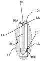
또한, 도 1에서 개략적으로 보여지는 바와 같이, 에어 갭 내에서 굽힘을 받는 접촉 프로브는 프로브 자체 또는 가이드들의 적절한 구성에 의해 도움을 받을 수 있는데, 도시의 단순화를 위해서, 테스트 헤드에 포함된 보수의 프로브들 중에서 단지 하나의 접촉 프로브가 소위 전환된 플레이트 유형의 테스트 헤드로서 보여진다. Further, as schematically shown in Fig. 1, the contact probe, which is subjected to bending in the air gap, may be assisted by proper configuration of the probe itself or guides, which, for simplicity of illustration, Only one of the probes is shown as a so-called switched plate type test head.
특히, 도 1에서 적어도 하나에서 접촉 프로브(4)가 슬라이딩하는 각각의 상부 가이드 홀(2A) 및 하부 가이드 홀(3A)를 구비하는 하나 이상의 상부 플레이트 또는 가이드(2) 및 하부 플레이트 또는 가이드(3)를 포함하는 테스트 헤드(1)가 개략적으로 도시된다.In particular, at least one of the upper plate or
접촉 프로브(4)는 하나 이상의 접속 단 또는 팁(4A)을 구비한다. 이하에서, 용어 단 또는 팁은 단부를 의미하고, 반드시 날카로운 부분을 의미하는 것은 아니다. 특히, 접촉 팁(4A)은 테스트 중인 디바이스(5)의 접촉 패드(5A)에 인접하고, 디바이스 및 테스트 장치(미도시) 사이의 전기적 및 기계적 접속을 실현하는데, 테스트 헤드는 단자 구성(terminal element)을 형성한다. The
어떤 경우에는, 접촉 프로브는 상부 가이드에서 헤드 자체에 고정되도록 결합되는데: 그런 경우에, 테스트 헤드는 막혀진-프로브 테스트 헤드(blocked-probe testing heads)라고 불리운다. In some cases, the contact probes are fixed to the head itself in the upper guide: in such cases, the test head is called blocked-probe testing heads.
대안적으로, 테스트 헤드는 고정되도록 결합되지 않고 마이크로 접속 보드에 의해 보드에 접속된(interfaced) 프로브를 구비하는데: 그러한 테스트 보드는 비차단 프로브 테스트 헤드(non-blocked probe testing heads)로 불리운다. 마이크로 접속 보드는 접촉 프로브 이외에도, 시험 중인 디바이스의 접촉 패드에 대해서 접촉 패드를 공간적으로 재분배하는 것을 허용하고, 특히 패드의 중앙 사이에서 거리 구속조건을 완화하기 때문에 소위 "공간 트랜스포머"로 불리운다. Alternatively, the test head has a probe interfaced to the board by a micro-connection board, which is not coupled to be fixed: such a test board is referred to as non-blocked probe testing heads. In addition to the contact probes, the micro-connection board also allows for the spatial redistribution of the contact pads relative to the contact pads of the device under test, and is called a so-called "space transformer" because it alleviates the distance constraint, especially between the centers of the pads.
도 1에 도시되는 이 경우에, 접촉 프로브(4)는 공간 트랜스포머(6)의 복수의 접촉 패드(6A)를 향하는, 보통 접촉 헤드로 구체화되는 추가의 접촉 팁(4A)을 구비한다. 프로브 및 공간 트랜스포머 사이의 우수한 전기적 접촉은 공간 트랜스포머(6)의 접촉 패드(6A)에 대하여 접촉 프로브(4)의 접촉 헤드(4B)를 가압하는 것에 의한 테스트 중인 디바이스와의 접촉과 유사하게 보장된다. In this case shown in Fig. 1, the
전술한 바와 같이, 상부(2) 및 하부(3) 가이드는 에어 갭(7)에 의해 적절히 분리되는데, 에어 갭(7)은 테스트 헤드(1)의 동작 동안의 접촉 프로브(4)의 변형을 허용하고 접촉 프로브(4)의 접촉 팁(4A) 및 접촉 헤드(4B)가 테스트 중인 디바이스(5)의 접촉 패드 및 공간 트랜스포머(6)에 각각 접속하는 것을 보장한다. 명백히, 상부(2A) 및 하부(3A) 가이드 홀은 접촉 프로브(4)가 내부에서 슬라이딩을 허용할 수 있기 위한 크기로 되어야 한다. As described above, the upper and
사실, 테스트 헤드의 적절한 동작이 두 파라미터들: 접촉 프로브의 초과 이동 거리(overtravel) 또는 수직적인 움직임 및 이런 프로브들의 접촉 팁의 스크럽(scrub) 또는 수평적인 움직임에 필수적으로 관련되는 점은 기억되어야 하고, "수평적인"은 테스트 중인 디바이스(5)와 실질적으로 같은 평면으로 움직여서 테스트 헤드(1)를 가이드하는 것을 의미하고, 반면에 "수직적인"은 테스트 중인 디바이스(5)와 실질적으로 수직으로 움직여서 테스트 헤드(1)를 가이드하는 것을 의미한다.In fact, it should be remembered that the proper operation of the test head is essentially related to both parameters: overtravel or vertical movement of the contact probe and scrub or horizontal movement of the contact tip of such probes Quot; horizontal "means guiding the
그러므로, 프로브 및 테스트 중인 디바이스 사이의 우수한 전기 접속이 항상 보장되어야 하기 때문에, 이런 특징들은 테스트 헤드의 제조 단계에서 평가 및 계산되어야 한다.Therefore, these features must be evaluated and calculated at the manufacturing stage of the test head, since good electrical connection between the probe and the device under test must always be ensured.
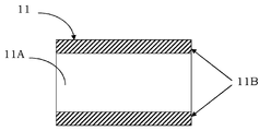
도 2에서 개략적으로 도시된 바와 같이, 길이 방향으로 실질적으로 연장되고 바람직하게는 금속 또는 특히, 니켈 망간(NiMn) 또는 니켈 코발트(NiCo)와 같은 합금인 제1 전도성 재료로 이루어진 바디(9A)에 의해 접촉 프로브(4)를 구현하는 것이 또한 알려져 있다. 그러므로, 이런 접촉 프로브들(4)은 테스트 헤드(1) 내부에 실질적으로 수직으로 위치된 길이 방향, 즉 가이드들 및 테스트 중의 디바이스에 수직 방향으로 배치된다. As shown schematically in Figure 2, a
바디(9A)는 실질적으로 기 설정된 길이를 갖는 중앙부(8C) 또는 정확히는 접촉단 또는 접촉팁(4A) 및 접촉단 또는 접촉 헤드(4B)인 접촉 팁 또는 양단을 구비한다. The
접촉팁(4A)은 기설정된 길이(8A)를 갖고, 접촉 프로브(4)의 사용 동안에 테스트 중인 디바이스의 접촉 패드에 가압 접촉을 하도록 의도된다.(미도시, 하지만 어쨌든, 도 1에서 도시된 테스트 중인 디바이스(5)의 접촉 패드(5A)에 완전히 유사하다). The
유사하게는, 특히 비차단 프로브의 테스트 헤드의 경우, 접촉 프로브(4)의 사용 동안에, 접촉 헤드(4B)는 차례로 기설정된 길이(8B)를 갖고 대신에 공간 트랜스포머의 접촉 패드에 가압 접촉하도록 의도된다(미도시, 하지만 어쨌든, 도 1에서 도시된 트랜스포머(6)의 접촉 패드(6A)에 완전히 유사하다). Similarly, in the case of a test head of a non-blocking probe, in particular, during use of the
동일 출원인을 위한, 2007년 11월 16일에 MI2007A002182호로 출원되고, 2010년 12월 23일에 특허허여된 이탈리아 특허 IT 1383 883호에서 서술된 바와 같이, 접촉 프로브(4)를 특히 바디(9A)로 구현되는 제1 전도성 재료 보다 높은 경도를 가지는 제2 전도성 재료의 층(9B)으로 코팅하는 것이 알려져 있다. 바람직하게는, 제2 전도성 재료는 로듐, 금, 플라티늄 또는 팔라듐-코발트(PdCo) 합금과 같은 금속 또는 합금일 수 있다. For the same applicant, the
아울러, 도 2에서 도시된 바와 같이, 바디(9A)의 중앙부는 예를 들면 패럴린(parylene), 특히 절연성 재료로 이루어진, 레이어(9B)로 또한 코팅될 수 있다.2, the central portion of the
이런 방식으로, 레이어(9B)에 의해 구현된 절연 코팅은, 접촉 프로브(4)의 전기적 절연성을 전체로서 향상시키고, 테스트 헤드(1)에서의 인접한 접촉 프로브들 사이에 우연한 접촉의 경우에서 단락을 방지한다. In this way, the insulating coating implemented by the
전술된 이탈리아 특허 출원에서 서술된 해결책은 특히, 접촉 프로브의 보다 큰 경도를 얻는 것과 동시에 다른 인접한 접촉 프로브들과의 우연한 접촉의 경우에 전기적 절연을 보장하는 것을 허용한다. The solution described in the above-mentioned Italian patent application permits, in particular, to ensure electrical insulation in case of accidental contact with other adjacent contact probes while achieving greater hardness of the contact probe.
그러나, 이런 해결책은 접촉 프로브의 헤드들과 팁들 및 각각의 접촉 패드들 사이의 전기적 접속 효율을 감소시킬 수 있다.However, such a solution can reduce the electrical connection efficiency between the heads and tips of the contact probes and the respective contact pads.
결점을 극복하기 위해 접촉 프로브의 단부, 특히 접촉 팁들 및/또는 접촉 헤드에서 고 전도성 금속 재료, 바람직하게는 금을 이용하여 코팅하는 것이 또한 알려져있다. It is also known to coat with the use of a highly conductive metal material, preferably gold, at the ends of the contact probes, especially the contact tips and / or the contact head, to overcome the drawbacks.
명백하게, 관련된 치수 및 관련된 재료의 비용은 이런 코팅 동작을 극도록 곤란하게 만든다.Obviously, the costs of the associated dimensions and associated materials make such coating operations extremely difficult.
때로는 접촉 프로브들을 공통이며 종종 복잡한 동작 상태로 있게 하는 것이 또한 필요한데 프로브들은, 보통 처리 프레임으로 불리우는 전용 지지부에 거치되고 위치되는 것이 요구된다. 프로브들은 처리 프레임에 거치되고 그 후 그들 전체 또는 특정 부분에 영향을 미치는 하나 이상의 동작을 수행한다. 그 후, 후의 테스트 헤드에 위치시키는 이후 처리를 위해 접촉 프로브들을 처리 프레임으로부터 제거하는 것이 명확히 필요하다. Sometimes it is also necessary to keep the contact probes in a common and often complex operating state, and the probes are required to be mounted and positioned on a dedicated support, usually referred to as a processing frame. The probes are placed in a processing frame and thereafter perform one or more operations that affect all or a specific part thereof. Thereafter, it is clearly necessary to remove the contact probes from the processing frame for later processing, which is then placed on the test head.
또한, 이런 경우에, 관련된 치수들은 접촉 프로브들의 동작들을 처리 프레임에 위치 및 거치하게 하고, 또한 그 후에 제거하는데, 이는 특히 생산 시간 및 소비와 관련하여 복잡하고 고가이다.Also in this case, the associated dimensions cause the movements of the contact probes to be placed in the processing frame and then removed, which is complicated and expensive, especially in terms of production time and consumption.
본 발명의 기술적인 문제는 프로브들이 반제품의 기판에서 적절히 구현되고 거기에 고정되는 복수의 테스트 헤드용 접촉 프로브들을 포함하는 반제품 및 이런 반제품을 얻을 수 있는 제조방법을 제공하는 것인데, 이런 특징들을 구비하는 방법 및 그것에 의해 얻어진 반제품은 간단하고 신뢰할만하고 보다 자주 반복될 수 있는 방식으로 복수의 접촉 프로브들에서의 다른 동작들 구현을 허용하는데, 이런 방식으로 종래 기술에 의해 수행되는 방법에 현재 영향을 미치는 결점 및 한계를 극복한다. The technical problem of the present invention is to provide a semi-finished product including contact probes for a plurality of test heads in which the probes are properly implemented and fixed on the substrate of the semi-finished product, and a manufacturing method for obtaining such semi-finished products, The method and the semi-finished product obtained thereby permit the implementation of other operations in a plurality of contact probes in a manner that is simple, reliable and can be repeated more often, Overcoming defects and limitations.
본 발명의 기초를 이루는 해결 과제는 많은 접촉 프로브들이 기판으로부터 제거 재료에 의해 반제품(semi-finished product)의 기판에서 얻어질 수 있는 반제품을 구현하는 것이고, 프로브들을 기판에 고정하기 위해 그것에 의해 적절한 기계적인 접촉 브릿지를 구비하는 프로브들이 구현되고, 이로 인해, 원하는 특징을 구비하는 접촉 프로브들이 얻어질 때까지, 반제품은 얻어진 모든 프로브들에 영향을 끼치는 하나 이상의 처리 단계들을 경험하고, 그 후 이런 프로브들은 반제품의 기판으로부터 쉽게 분리된다. The underlying problem of the present invention is to realize a semi-finished product in which many contact probes can be obtained from a substrate of a semi-finished product by a removal material from the substrate, Probes with contact bridges are implemented so that until the contact probes with the desired characteristics are obtained, the semi-finished product experiences one or more processing steps that affect all the probes obtained, And is easily separated from the substrate of the semi-finished product.
이런 해결 과제에 기초하여, 기술적인 문제는 전자 디바이스의 복수의 테스트 헤드용 접촉 프로브를 포함하는 반제품의 제조방법에 의해 해결되는데, 상기 방법은: Based on this solution, a technical problem is solved by a method of manufacturing a semi-finished product comprising a plurality of contact probes for a test head of an electronic device, the method comprising:
- 전도성 재료로 이루어진 기판을 제공하는 단계; 및- providing a substrate made of a conductive material; And
- 하나 이상의 브릿지 재료에 의해 상기 접촉 프로브들 각각이 상기 기판에 고정되도록 상기 기판으로부터 재료를 제거함으로써 상기 접촉 프로브들 각각을 형성하는 단계를 포함하고, 상기 접촉 프로브들을 형성하는 단계는, 상기 접촉 프로브들 및 상기 하나 이상의 브릿지 재료의 형태에 대응한 레이저 커팅 단계를 포함한다. - forming each of the contact probes by removing material from the substrate such that each of the contact probes is secured to the substrate by one or more bridging materials, And a laser cutting step corresponding to the shape of the at least one bridge material.
본 발명의 다른 측면에 의하면, 상기 접촉 프로브들을 형성하는 단계는, 상기 기판을 마스킹하고 에칭하는 하나 이상의 단계 또는 상기 기판을 선택적으로 화학적 에칭하는 단계를 선택적으로 포함하는, 상기 기판의 마스킹 처리 및 후속의 화학적 에칭에 의한 포토리소그래피 에칭 단계를 포함할 수 있다. According to another aspect of the present invention, the step of forming the contact probes comprises selectively masking and etching the substrate, wherein the step of selectively masking and subsequently etching the substrate comprises: And a photolithographic etching step by chemical etching of the substrate.
특히, 상기 형성하는 단계는, 상기 접촉 프로브들 각각을 따라서, 대칭 또는 비대칭의, 완전히 임의적인 방식으로 위치되고, 복수의 브릿지 재료 각각에 의해 상기 기판에 고정된 상기 접촉 프로브들을 구현할 수 있다. In particular, the forming step may implement the contact probes fixed in the substrate by each of the plurality of bridging materials, in a completely random manner, either symmetrically or asymmetrically, along each of the contact probes.
아울러, 본 발명의 또 다른 측면에 의하면, 상기 형성하는 단계는, 바람직하게 상기 접촉 프로브들의 접촉 팁을 포함하는 제1단부에 대응되는, 중앙 위치에 위치된 하나 이상의 제1 브릿지 재료 및 바람직하게 상기 접촉 프로브의 접촉 헤드를 포함하는 제2단부에 대응되는 측면 위치에 위치된 하나의 제2 브릿지 재료를 포함하는 상기 접촉 프로브들 각각을 구현할 수 있다. According to still another aspect of the present invention, the forming step comprises at least one first bridge material positioned at a central position, preferably corresponding to a first end comprising a contact tip of the contact probes, Each of the contact probes comprising a second bridge material positioned at a side position corresponding to a second end comprising a contact head of the contact probe.
더욱이, 상기 형성하는 단계는, 상기 브릿지 재료 각각에 그것을 통과하고 상기 브릿지 재료의 무결성(integrity)을 파손하도록 상기 기판으로부터 상기 접촉 프로브의 분리를 가능하게 이루어지는 하나 이상의 약화선을 장착하는 단계를 포함할 수 있고, 상기 하나 이상의 약화선은 상기 반제품의 평면에 수직인 방향을 따라서, 상기 기판의 대응되는 국부 세선에 의해 얻어진다. Moreover, the forming step includes mounting at least one weakening line through each of the bridge materials, the at least one weakening line being adapted to allow separation of the contact probe from the substrate so as to break the integrity of the bridging material And the at least one weakening line is obtained by a corresponding local fine line of the substrate along a direction perpendicular to the plane of the semi-finished product.
본 발명의 또 다른 측면에 의하면, 상기 기판을 제공하는 단계는,According to another aspect of the present invention,
- 전도성 재료로 이루어진 단일층을 제공하는 단계; 또는Providing a single layer of conductive material; or
- 전도성 재료로 이루어진 하나 이상의 코팅층에 의해 덮여진 제1 전도성 재료로 이루어진 중앙층 또는 코어를 포함하고, 상기 기판에서 구현된 상기 접촉 프로브들의 경도에 대한 성능 및/또는 전자 기계 성능을 향상시키기에 적합한 다층을 제공하는 단계 중 하나를 포함할 수 있다. - a central layer or core of a first conductive material covered by at least one coating layer of a conductive material, said core or core being suitable for enhancing the performance and / or electromechanical performance of the contact probes implemented in the substrate And providing a multi-layer.
아울러, 상기 제조방법은 코팅 단계, 덮는 단계, 레이저, 포토리소그래피 또는 전기 아연 도금 형성 단계, 전기 도금 단계, 전기 아연 도금 증착 단계, 정밀기계 처리 단계, 스퍼터링 단계, 화학적 또는 물리적 에칭 단계로부터 선택된 하나 이상의 단계를 포함하는, 상기 반제품에 포함된 상기 접촉 프로브들 모두와 관련된 하나 이상의 처리 단계를 포함할 수 있다. In addition, the manufacturing method may further comprise at least one selected from a coating step, a covering step, a laser, a photolithography or electro-galvanizing step, an electroplating step, an electro-galvanizing deposition step, a precision machining step, a sputtering step, And at least one processing step associated with all of the contact probes included in the semi-finished product,
특히, 상기 처리 단계는 전체적으로 모든 상기 접촉 프로브들 또는 상기 접촉 프로브들의 하나 이상의 부분에 영향을 미칠수 있다. In particular, the processing step may affect the entire contact probes or one or more portions of the contact probes as a whole.
아울러, 상기 처리 단계는 상기 반제품의 같거나 다른 부분들을 위한 같은 종류의 다수의 반복되는 단계들을 포함할 수 있다. In addition, the processing step may comprise a number of repeated steps of the same kind for the same or different parts of the semi-finished product.
본 발명의 또 다른 측면에 의하면, 상기 처리 단계는 전도성 재료 및 유전성 재료로부터 선택된 코팅 재료로 이루어진 코팅 필름의 구현으로 하나 이상의 상기 반제품 및 상기 접촉 프로브들 또는 그것의 일부분을 코팅하는 하나 이상의 단계를 포함할 수 있다. According to another aspect of the present invention, the processing step comprises one or more steps of coating one or more of the semi-finished products and the contact probes or a portion thereof with an implementation of a coating film comprised of a coating material selected from a conductive material and a dielectric material can do.
특히, 상기 코팅하는 단계는 상기 반제품의 하나 이상의 코팅부 상에 상기 코팅 필름을 구현할 수 있고, 상기 하나 이상의 코팅부는 상기 반제품에서 구현된 상기 접촉 프로브들의 접촉 팁 또는 접촉 헤드를 포함하는 부분을 의미하는 상기 반제품의 단부에 배치되고, 및/또는 상기 하나 이상의 코팅부는 상기 반제품에서 구현된 상기 접촉 프로브들의 접촉 팁 및 접촉 헤드를 포함하지 않는 부분을 의미하는 상기 반제품의 중앙부에 배치된다.In particular, the coating step may embody the coating film on at least one coating part of the semi-finished product, wherein the at least one coating part means a part comprising the contact tip or contact head of the contact probes embodied in the semi-finished product And / or the at least one coating portion is disposed at a central portion of the semi-finished product, which means a portion not including the contact tip and the contact head of the contact probes implemented in the semi-finished product.
보다 구체적으로, 상기 코팅하는 단계는 팔라듐 또는 니켈-팔라듐과 같은 팔라듐 합금, 구리, 및 구리- 니오븀 또는 구리-은과 같은 구리 합금, 로듐 및 로듐의 합금, 은 또는 금이나 이들의 합금들로부터 선택된 금속 또는 합금으로 이루어지거나, 또는 그래핀으로 이루어지거나, 또는 도핑된 DLC ("다이아몬드상 카본", "Diamond Like Carbon")로 이루어지고, 바람직하게는 귀금속들의 그룹으로부터 선택되거나, 보다 바람직하게는 금으로 이루어진 전도성 재료의 상기 코팅 필름을 구현할 수 있다. More specifically, the coating is selected from palladium alloys such as palladium or nickel-palladium, copper and copper alloys such as copper-niobium or copper-silver, alloys of rhodium and rhodium, silver or gold or alloys thereof (Or "Diamond Like Carbon"), preferably made of a group of precious metals, more preferably made of a metal or an alloy, or made of graphene or doped DLC ≪ / RTI > can be realized.
대안적으로, 상기 코팅하는 단계는 플루오르화 폴리머, 폴리(p-자일릴렌) 폴리머, 바람직하게는 특히 C 타입 또는 F 타입의 패럴린®, 그것의 공중합체 또는 나노복합체 또는 도핑되지 않은 DLC, 바람직하게는 C 타입 또는 F 타입의 패럴린®으로부터 선택된 유전성 재료의 상기 코팅 필름을 구현할 수 있다. Alternatively, the coating may be carried out using a fluoropolymer, a poly (p-xylylene) polymer, preferably a C or F type paralin, a copolymer or nanocomposite thereof or an undoped DLC, Lt; RTI ID = 0.0 > of C < / RTI > type or F type of Parallel.
본 발명의 또 다른 측면에 의하면, 상기 코팅하는 단계는: According to another aspect of the present invention, the coating comprises:
- 침적 용기의 탱크 내의 액상인 코팅 재료에서 상기 반제품을 담그고, 상기 액상인 코팅 재료는 상기 탱크를 상기 코팅 필름에 의해 코팅된 상기 반제품의 부분을 결정하도록 이루어지는 코팅 레벨까지 채우는 과정; 또는Dipping said semi-finished product in a liquid phase coating material in a tank of a dipping vessel, said liquid phase coating material filling said tank to a coating level which is adapted to determine said portion of said semi-finished product coated by said coating film; or
- 상기 코팅 필름에 의해 코팅된 상기 반제품의 하나 이상의 부분에 대응되는 증기상인 코팅 재료를 분사하도록 이루어진 하나 이상의 노즐이 장착된, 증발 챔버에서 상기 반제품의 삽입하는 과정으로부터 선택될 수 있다. - the process of inserting the semi-finished product in the evaporation chamber, which is equipped with one or more nozzles adapted to emit coating material which is a vapor phase corresponding to one or more parts of the semi-finished product coated by the coating film.
더욱이, 상기 코팅하는 단계는 음극 스퍼터링 처리에 의해 구현되는 하나 이상의 재료 증착 단계를 포함할 수 있고, 에너지 입자 빔으로 충격이 가해지고 상기 반제품의 표면 상에 재응결될 때 원자, 이온 또는 분자 파편은 타겟으로 불리우는 고체 재료에 의해 배출되고, 상기 반제품이 적절히 충격이 가해진 상기 타겟 코팅 재료와 함께 특수 진공 챔버에 위치될 때 그 안에서 만들어진 상기 접촉 프로브들의 범위의 전체 또는 부분에서 만들어진다. Moreover, the coating may include one or more material deposition steps implemented by a cathodic sputtering process, wherein when an impact is applied to the energy particle beam and the surface of the semi-finished product is recondensed, atoms, ions or molecular debris Is produced in all or part of the range of contact probes made therein when the semi-finished product is placed in a special vacuum chamber with the suitably impacted target coating material.
본 발명의 또 다른 측면에 의하면, 상기 제조방법은 상기 반제품의 부분, 바람직하게는, 상기 접촉 팁 및 상기 접촉 헤드 모두를 포함하지 않는 것을 의미하는 부분인 상기 접촉 프로브들의 중앙부에 대응되는 부분에서 하나 이상의 덮는 필름을 구현하도록 상기 반제품의 하나 이상의 부분의 유전성의 덮는 재료에 의해 덮는 단계를 더 포함할 수 있다. According to another aspect of the present invention, there is provided a method of manufacturing a semiconductor device, comprising the steps of: (a) forming a contact tip on a semiconductor wafer, Of the at least one portion of the semifinished product so as to implement the overlying film. ≪ RTI ID = 0.0 > [0031] < / RTI >
아울러, 상기 덮는 단계는 접촉 프로브를 덮는 재료로 전체 코팅 단계 및 다음의 반제품을 마스킹하고 관심의 부분에서 덮는 필름을 구현하는 접촉 프로브의 관심 부분의 외부에서 덮개 재료를 제거하는 단계를 포함할 수 있다. In addition, the covering step may include the entire coating step with the material covering the contact probe and masking the next semi-finished product and removing the cover material from outside the area of interest of the contact probe that implements the film covering in the area of interest .
마지막으로, 본 발명은 또한 복수의 테스트 헤드용 접촉 프로브를 포함하는 반제품에 관한 것이고, 각각의 접촉 프로브들은 전도성 재료의 기판에서 구현되고 하나 이상의 브릿지 재료에 의해 기판에 고정된다. Finally, the present invention also relates to a semi-finished product comprising a contact probe for a plurality of test heads, wherein each contact probe is embodied in a substrate of conductive material and secured to the substrate by one or more bridging materials.
본 발명에 의한 반제품 및 제조방법의 특성 및 장점은 이하에서 첨부된 도면들을 참조하여 제한되지 않은 예시 및 표시들에 의해 주어지는, 그들의 일 실시예로 설명될 것이다. The characteristics and advantages of the semi-finished product and the manufacturing method according to the present invention will be described below by way of an embodiment thereof, given by way of non-limitative examples and indications, with reference to the accompanying drawings.
도 1 및 2는 종래 기술로 구현되는 테스트 헤드용 접촉 프로브들을 도시하는 개략도.
도 3a 및 3b, 4a 내지 4b, 및 5a 내지 5b는 본 발명에 의한 복수의 접촉 프로브들을 포함하는 반제품의 대안적 실시예들을 도시하는 개략도 및 관련된 단일 프로브와 대응되는 상세도.
도 6a 내지 6c는 본 발명에 의한 반제품용 기판의 대안적 실시예들을 도시하는 개략도.
도 7a 내지 7c는 본 발명에 의한 제조방법에 대응되는 다양한 단계들 동안의 도 5a의 반제품을 도시하는 개략도.
도 8a 내지 8d는 본 발명에 의한 반제품의 제조 방법의 다양한 단계를 도시하는 개략도.
도 9a 내지 9c는 도 8a 내지 8d에 관한 변형례에 의한 본 발명의 제조방법에 의해 구현된 반제품의 대안적 실시예들을 도시하는 개략도.
도 10a 내지 10d는 도 9a 내지 9c를 참고하여 도시한 대안적 실시예들에 의한 본 발명의 반제품으로부터 얻어진 접촉 프로브를 도시하는 개략도.
도 11a 및 11b는 본 발명에 의한 반제품의 대안적 실시예들을 도시하는 개략도.
도 12a 및 12b는 본 발명에 의한 제조방법의 일 단계를 도시하는 개략도.
도 13은 도 12a 및 12b를 참고하여 도시한 본 발명의 제조방법에 의해 구현된 본 발명에 의한 반제품의 추가적인 대안적 실시예를 도시하는 개략도.
도 14a 내지 14d는 도 13의 반제품으로부터 시작된 본 발명의 대안적 실시예들에 의한 제조방법의 일 단계를 도시하는 개략도.
도 15a 내지 15c는 도 14a 내지 14d를 참고하여 도시한 변형례에 의한 발명의 제조방법에 의해 구현된 반제품의 대안적 실시예를 도시하는 개략도.
도 16a 내지 16c는 도 15a 내지 15c를 참고하여 도시한 대안적 실시예에 의한 반제품으로부터 얻어진 접촉 프로브를 도시하는 개략도.Figures 1 and 2 are schematic diagrams showing contact probes for a test head embodied in the prior art;
Figures 3a and 3b, 4a-4b, and 5a-5b are schematic diagrams illustrating alternative embodiments of a semi-finished product including a plurality of contact probes in accordance with the present invention, and corresponding detail views of a single probe.
6A to 6C are schematic diagrams showing alternative embodiments of a substrate for a semi-finished product according to the present invention.
Figures 7a to 7c are schematic diagrams showing the semi-finished product of Figure 5a during various stages corresponding to the manufacturing method according to the invention.
8A to 8D are schematic views showing various steps of a method of manufacturing a semi-finished product according to the present invention.
Figures 9a to 9c are schematic diagrams showing alternative embodiments of the semi-finished product implemented by the manufacturing method of the present invention according to a variant of Figures 8a to 8d.
Figs. 10a to 10d are schematic diagrams showing contact probes obtained from the semi-finished product of the present invention according to alternative embodiments shown with reference to Figs. 9a to 9c. Fig.
11A and 11B are schematic diagrams showing alternative embodiments of semi-finished products according to the present invention.
12A and 12B are schematic diagrams showing one step of a manufacturing method according to the present invention.
Figure 13 is a schematic diagram showing a further alternative embodiment of a semi-finished product according to the invention embodied by the manufacturing method of the present invention, with reference to Figures 12a and 12b.
Figures 14a-14d are schematic diagrams showing one step of a manufacturing method according to alternative embodiments of the present invention starting from the semi-finished product of Figure 13;
15A to 15C are schematic diagrams showing an alternative embodiment of a semi-finished product realized by the manufacturing method of the invention according to the modification shown with reference to Figs. 14A to 14D. Fig.
16A to 16C are schematic views showing a contact probe obtained from a semi-finished product according to an alternative embodiment shown with reference to Figs. 15A to 15C. Fig.
상기 도면들 특히 도 3a 및 3b, 4a 내지 4b, 및 5a 내지 5b를 참조하여, 복수의 테스트 헤드용 접촉 프로브들을 포함하는 반제품이 서술되는데, 반제품은 전체적으로 부로 15로 지시된다. 3A and 3B, 4A to 4B, and 5A to 5B, there is described a semi-finished product including a plurality of contact probes for a test head, the semi-finished product being indicated generally at 15.
상기 도면들은 개략도를 나타내는데, 비율에 맞게 도시되지 않았고, 대신에 본 발명의 중요한 특징을 강조하기 위해 도시된 점이 주목되어야 한다.It should be noted that the figures represent schematic representations, not drawn to scale, and are instead shown to emphasize important features of the present invention.
아울러, 이하에서 서술되는 방법의 단계들은 접촉 프로브들 및 반제품의 제조를 위한 완전한 처리 흐름을 형성하지 않는다. 본 발명은 최근에 기술 분야에서 사용되는 제조기술들과 함께 실행될 수 있는데, 본 발명의 이해를 위해 필요한 처리 단계들이 이용되는 보통의 제조기술들만을 포함된다.In addition, the steps of the method described below do not form a complete process flow for the production of contact probes and semi-finished products. The present invention can be practiced in conjunction with the manufacturing techniques used in the art recently, including only ordinary manufacturing techniques in which the necessary processing steps are used for an understanding of the present invention.
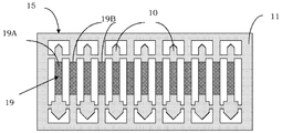
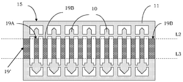
더욱 구체적으로, 도 3a에서 개략적으로 도시된 바와 같이, 반제품(15)는 전도성 재료로 이루어진 기판(11)에 의해 구현된 복수의 접촉 프로브들(10)을 포함한다. More specifically, as schematically shown in Fig. 3A, the
특히 각각의 접촉 프로브(10)는 간단히 프레임(12)을 가리키는 실질적으로 프레임 형상의 적절한 리세스에서 구현되고, 접촉 프로브(10)를 둘러싼 재료를 제거하는 것에 의해 기판(11)에서 구현된다. In particular, each
유리하게는, 본 발명에 의하면, 각각의 접촉 프로브(10)는 하나 이상의 브릿지 재료(13)에 의해 기판(11)에 고정된다. Advantageously, according to the invention, each
특히, 도 3a 및 3b에 도시된 예에서, 각각의 접촉 프로브(10)는 대응되는 프레임(12) 내부에서 기판(11)에 연결하여 고정시키는 하나의 브릿지 재료(13)를 구비하는데, 브릿지 재료(13)는 프로브 부분에서 구현되는데, 바람직한 실시예에서 부분은 단부와 다른데, 용어 단부는 접촉 프로브(10)의 접촉 팁(10A) 또는 접촉 헤드(10B)를 포함하는 부분을 의미한다. 3A and 3B, each of the contact probes 10 has one
적절하게는, 도 3b에 도시되는 바와 같이, 접촉 프로브(10) 각각의 브릿지 재료(13)에는 그것을 통과하는 하나 이상의 약화선(weakening line, LL)이 장착되는데 이는 브릿지 재료(13)의 무결성을 파손하도록 기판(11)으로부터 프로브의 분리를 활용하도록 이루어진다.3B, the
도 3a 및 3b에 도시된 실시예에서, 각각의 브릿지 재료(13)는 접촉 프로브(10) 근처에 위치된 약화선(LL)을 구비하는데, 그것의 파손은 접촉 프로브(10)가 기판(11)으로부터 분리될 때 기판(11)에 고정된 브릿지 재료(13) 대부분의 유지를 야기시킨다.3a and 3b, each
적절하게는, 약화선(LL)은 기판(11)을 드릴 작업에 의해 얻어질 수 있는데, 드릴 작업은 어떠한 형상도 가질 수 있는데, 예를 들면 원형, 타원형, 직사각형, 이들 중 어느 것이 틸팅된 것일 수 있다. 대안적으로, 본 발명에 의한 반제품(15)의 바람직한 실시예에 의하면, 반제품(15) 그 자체의 평면에 수직인 Z 방향에 따르는 약화선(LL)은 그것에 대응되는 기판(11)의 국부 세선(local thinnig)에 의해 얻어질 수 있다. Optionally, the weakening line LL can be obtained by drilling the
명백하게는, 완전히 임의적인 방식으로 도 3a 및 3b에서 도시되는 것에 관한 접촉 프로브(10)의 다른 점들에서 또한 위치되는, 어떠한 수의 브릿지 재료(13)를 구현하는 것이 가능하다. Obviously, it is possible to implement any number of bridging
특히, 도 4a 및 4b에 도시된 대안적인 실시예에서, 본 발명에 의한 반제품(15)은 기판(11) 내에 구현된 복수의 접촉 프로브들(10)를 포함하는데, 각각의 접촉 프로브(10)는 복수의 복수의 브릿지 재료(13) 각각에 의해 기판(11)에 고정된다.4a and 4b, the
도 4b에 도시된 확대도에서 강조되는 바와 같이, 각각의 접촉 프로브(10)는 4개 이상의 브릿지 재료(13)에 의해 기판(11)에 고정되는데, 브릿지 재료의 제1쌍은 일 예에서 접촉 팁(10A)을 포함하는 그것의 단부에서 구현되고, 접촉 헤드(10B)를 포함하는 추가의 단부에서 구현된 브릿지 재료의 제2쌍에 의해 각각의 접촉 프로브(10)는 기판(11)에 고정되며, 이러한 브릿지 재료(13)의 제1 및 제2쌍들은 접촉 프로브(10)의 길이방향 축(YY)에 대하여 대칭으로 배치된다. 명백하게는, 각각의 접촉 프로브(10)를 위해 4개 보다 많거나 적은 브릿지 재료(13)를 제공하는 것은 가능한데, 브릿지 재료(13)는 길이방향 축(YY)에 대하여 대칭 또는 비대칭으로, 프로브 부분들에 대해 어느 위치에라도 위치된다. Each of the contact probes 10 is fixed to the
또한, 도 4b에 도시되는 경우에 있어서, 브릿지 재료(13)는 접촉 프로브(10) 근처에 위치된 약화선(LL)을 구비할 수 있고, 그것의 파손은 접촉 프로브(10)가 기판(11)으로부터 분리될 때 기판(11)에 고정된 브릿지 재료(13)의 대부분을 유지시킨다.4B, the bridging
도 5a 및 5b에 개략적으로 도시된 바람직한 실시예에서, 도면들에 도시된 바와 같이 반제품(15)은, 하나가 접촉 팁(10A), 바람직하게는 중앙 위치에서 구현되고, 다른 하나가 접촉 헤드(10B), 바람직하게는 측면 위치에서 구현되는 단지 2개의 브릿지 재료(13)에 의해 기판(11)에 각각 고정되는, 복수의 접촉 프로브들(10)을 포함한다.In the preferred embodiment schematically depicted in Figures 5A and 5B, the
서로 대칭적으로, 접촉 팁(10A), 바람직하게는 중앙 위치에서 구현된 브릿지 재료(13)와 접촉 헤드(10B), 바람직하게는 측면 위치에서 구현된 한 쌍의 추가된 브릿지 재료(13)에 의해 기판(11)에 고정되도록 각각의 접촉 프로브(10)가 구현되는 실시예 또한 바람직하다(미도시).Symmetrically with respect to one another, a
접촉 프로브(10)의 접촉 팁(10A) 단부에 하나 이상의 브릿지 재료(13)를 포지셔닝하는 것은 이런 프로브들의 단부에 작용하는 후처리 동작을 포함하는 접촉 프로브 제조 방법에서 특히 유리한데; 이 경우에, 기판(11)으로부터 접촉 프로브들(10)을 분리시킨 후에 예를 들면 접촉 프로브들(10)의 접촉 팁들(10A)에서의 이런 단부들의 재형성 동작에 대한 이행되는 점을 고려하는데, 약화선(LL)의 파손 및 브릿지 재료(13)의 제거로 인한 불완전함 또는 버를 제거하는 것을 허용하는 것이 강조되어야 한다.Positioning one or
이런 방식으로, 얻어진 접촉 프로브들(10)의 기계적 및 전기적 동작의 향상과 가공된 단부들의 부식에 대한 저항의 향상이 달성될 수 있다.In this way, improved mechanical and electrical operation of the contact probes 10 obtained and improved resistance to corrosion of the machined ends can be achieved.
아울러, 이런 단부들이 재형상 단계 후에는 더 이상 거칠지 않기 때문에 접촉 프로브들(10)의 슬라이딩의 향상, 특히 테스트 중인 디바이스의 접촉 패드들 각각에서의 접촉 팁들(10A)의 슬라이딩을 향상시킨다. This also improves the sliding of the contact probes 10, especially the sliding of the
전술한 대안적인 실시예들, 예를 들면 접촉 프로브들(10)의 접촉 팁들(10A)에서 구현된 단지 하나의 브릿지 재료(13) 및 적어도 다른 브릿지 재료(13) 또는 단부와 다른 위치, 예를 들면 중앙 위치에서 구현된 한쌍의 브릿지 재료(13)를 제공하는 실시예들을 결합하는 것은 명백히 가능하다.It will be appreciated that alternative embodiments described above may be used in place of, for example, only one
적절하게는, 기판(11)은 전자 디바이스를 위한 테스트 헤드용 접촉 프로브들을 구현하기 위해 적합한 전도성 재료로 이루어진다. Suitably, the
보다 구체적으로, 도 6a 내지 6c에서 도시되는 바와 같이, 기판(11)은 전자 디바이스를 위한 테스트 헤드용 접촉 프로브들을 구현하기 위해 적합한 단일층 또는 다층의 전도성 재료로 이루어질 수 있다. More specifically, as shown in Figs. 6A-6C, the
예를 들면, 기판(11)은 니켈 또는 니켈-마그네슘, 니켈-코발트, 니켈-철, 니켈-베릴륨 합금들과 같은 니켈 합금, 텅스텐 또는 텅스텐-구리, 텅스텐-레늄과 같은 텅스텐 합금, 구리 또는 구리-베릴륨, 구리-은, 구리-니오븀과 같은 구리 합금, 로듐 또는 로듐-루디늄과 같은 로듐 합금, 이리듐 또는 이리듐 합금 또는 실리콘과 같은 반도체 재료의 금속 또는 합금으로 이루어진 단일층일 수 있다. For example, the
특히, 전도성 재료는 전기 저항도 값이 20μΩ/cm 이하가 되도록 선택된다. In particular, the conductive material is selected to have an electrical resistance value of 20 mu OMEGA / cm or less.
대안적으로, 기판(11)은 전도성 다층일 수 있고, 특히 도 6b 및 6c에서 도시된 바와 같이, 다층 기판(11)으로부터 구현된 접촉 프로브의 전기-기계적 성능 및/또는 경도 성능을 향상시키기에 적합한, 하나 이상의 코팅층, 예를 들면, 제1코팅층(11B) 및 제2코팅층(11C)에 의해 덮여진 하나 이상의 중앙층 또는 코어(11A)를 포함할 수 있다. Alternatively, the
특히, 코어(11A)는 전술한 단일층 기판(11) 하나로부터 선택된 금속 또는 합금으로 이루어질 수 있고, 구리, 은, 팔라듐 또는 이들의 합금으로부터 선택되거나 고 전도성 값을 가지는 전도성 재료 및/또는 그래핀으로 이루어지거나 로듐, 루디늄 니켈-인, 니켈-팔라듐, 팔라듐 및 이들의 합금으로부터 선택되거나, 그래핀으로 이루어지거나 또는 도핑 또는 도핑되지 않은 DLC("diamond like carbon", "다이아몬드상 카본")로 이루어진 고 전도값을 가지는 전도성 재질로 이루어진 하나 이상의 코팅층에 의해 덮여질 수 있다. In particular, the
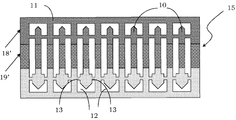
반제품(15)은 도 7a 내지 7c를 참고하여 도시된 제조방법에 의해 얻어진다. 특히, 도 4a에 도시된 반제품(15)의 실시예를 참조하여 서술되지만, 이하에서 서술된 방법은 도 3a 및 5a에서 도시된 실시예와 전술한 변형례에 의한 반제품(15)을 구현하기 위해 사용될 수 있다는 점이 강조되어야 한다. The
본 발명에 의한 반제품(15)의 제조방법은:A method of producing a semi-finished product (15) according to the present invention comprises:
- 도 7a에서 도시되는 바와 같이, 전도성 재료로 이루어진 기판(11)을 제공하는 단계; 및- providing a substrate (11) made of a conductive material, as shown in Figure 7a; And
- 상기 기판(11)으로부터 재료를 제거함으로써 상기 접촉 프로브들(10) 각각을 형성하는 단계를 포함한다. - forming each of said contact probes (10) by removing material from said substrate (11).
특히, 도 7b에 도시되는 바와 같이, 각각의 접촉 프로브(10)는 간단히 프레임(12)으로 보여지는 바와 같이, 필수적으로 프레임-형상이고, 적절한 리세스에서 구현되는데, 재료를 제거하고 접촉 프로브(10)를 둘러싸도록 기판(11)에서 구현된다. In particular, as shown in FIG. 7B, each
유리하게는, 본 발명에 의하면, 형성하는 단계는 하나 이상의 브릿지 재료(13)에 의해 기판(11)에 고정되도록 접촉 프로브(10)를 구현한다. 도 7b에서 보여진 예에서, 접촉 프로브(10)는 예를 들면 접촉 팁(10A)의 단부에서 구현되는 제1쌍의 브릿지 재료 및 예를 들면 접촉 헤드(10B)의 추가의 단부에서 구현되는 제2쌍의 브릿지 재료에 의해 기판(11)에 고정된다. Advantageously, according to the invention, the forming step implements the
적절하게는, 도 7c에서 개략적으로 도시되는 바와 같이, 형성하는 단계는 복수의 프레임(12)에서 복수의 접촉 프로브들(10)의 구현을 허용하되, 각각의 접촉 프로브(10)가 각각의 프레임(12)에 의해 둘러쌓이고 복수의 브릿지 재료(13) 각각에 의해 기판(11)에 고정되는 것을 허용한다. 도시된 실시예에서 반제품(15)의 접촉 프로브들(10)은 기하학적으로 같은 구성을 가지고, 특히 각각의 프레임(12)과 브릿지 재료(13)는 같은 부호 및 위치를 가지는데, 형성하는 단계는 프레임이 기판(11)에 포함되어 있는 한, 어느 형상 및 치수를 가지는 복수의 프레임(12)에서 복수의 접촉 프로브들(10)의 구현을 허용하고 접촉 프로브들(10)은 하나 이상의 브릿지 재료(13)에 의해 기판(11)에 고정되는 점이 강조되어야 한다.7C, the forming step permits the implementation of a plurality of contact probes 10 in a plurality of
기판(11)에서 접촉 프로브들(10)을 형성하는 단계는 프레임(12)을 개방시키기 위해 기판(11)으로부터 재료의 제거를 특히 제공한다. The step of forming the contact probes 10 in the
바람직한 실시예에서, 형성하는 단계는 프로브들(10) 및 브릿지 재료들(13)의 형태에 특히 대응한 레이저를 커팅하는 단계를 포함한다. In a preferred embodiment, the forming step comprises cutting the laser, particularly corresponding to the shapes of the
대안적으로, 형성하는 단계는 하나 이상의 마스킹 및 에칭 단계들을 차례로 포함할 수 있는 마스킹 처리 및 순차적인 화학적 에칭에 의한 포토리소그래피 에칭 단계(photolithographic etching step)를 포함한다. 형성하는 단계는 선택적인 기판(11)의 화학적 에칭 단계를 또한 포함할 수 있다. Alternatively, the forming step includes a masking process, which may in turn include one or more masking and etching steps, and a photolithographic etching step by sequential chemical etching. The forming step may also comprise a chemical etching step of the
도 7c에서 도시되는 바와 같이, 형성하는 단계의 끝에서, 브릿지 재료(13)에 의해 모두가 기판(11)에 여전히 고정되는 복수의 접촉 프로브들(10)을 포함하는 반제품(15)이 얻어진다. 7C, at the end of the forming step, a
아울러, 반제품(15)의 제조방법은 포함된 모든 접촉 프로브들(10) 위로 수행되는 하나 이상의 처리하는 단계를 포함할 수 있다. In addition, the manufacturing method of the
특히, 처리하는 단계는 동시에 또는 차례로 반제품(15)의 접촉 프로브들(10) 모두 또는 일부와 관련될 수 있다. In particular, the treating step may be associated with all or a portion of the contact probes 10 of the
반제품(15)의 접촉 프로브들(10) 모두와 관련된 처리하는 단계는 코팅 단계, 덮는 단계, 레이저, 포토리소그래피(photolithographic) 또는 전기 아연 도금 형성(electrogalvanic defining) 단계, 전기 도금(electroplating) 단계, 전기 아연 도금 증착(electrogalvanic deposition) 단계, 정밀기계 처리 단계, 스퍼터링 단계, 물리적 또는 화학적 에칭 단계, 이들 중 어떤 것으로부터 선택된 하나 이상의 단계를 포함한다. The processing steps associated with all of the contact probes 10 of the
처리하는 단계는 접촉 프로브들(10)의 하나 이상의 부분, 바람직하게는 접촉 프로브(10)의 접촉 팁(10A) 또는 접촉 헤드(10B)를 포함하는 부분을 의미하는 단부, 또는 접촉 프로브(10)의 접촉 팁(10A)과 접촉 헤드(10B)를 포함하지 않는 부분을 의미하는 중앙부로부터 선택된 부분에 특히 영향을 미칠 수 있다. The processing step may be performed at one or more portions of the contact probes 10, preferably at the end of the
대안적으로, 처리하는 단계는 접촉 프로브들(10) 전체에 영향을 미칠 수 있다. Alternatively, the processing step may affect the entire contact probes 10.
처리하는 단계는 반제품(15)의 같거나 다른 부분들을 위한 같은 종류의 다수의 반복되는 단계들을 또한 포함할 수 있다. The processing step may also include a number of repeated steps of the same kind for the same or different parts of the
도 8a 내지 8d에 개략적으로 도시된, 본 발명의 바람직한 실시예에서, 처리하는 단계는 반제품(15) 및 거기에 포함된 접촉 프로브들(10)을 코팅하는 단계를 포함한다.In a preferred embodiment of the present invention, schematically illustrated in Figures 8A-8D, the processing step comprises coating the
특히, 코팅하는 단계는 전도성 재료 및 유전성 재료로부터 선택된 코팅 재료로 이루어진 코팅 필름의 구현을 제공할 수 있다. In particular, the coating step may provide an implementation of a coating film comprised of a coating material selected from a conductive material and a dielectric material.
전도성의 코팅 재료의 경우, 팔라듐 또는 니켈-팔라듐과 같은 팔라듐 합금, 구리 및 구리-니오븀 또는 구리-은과 같은 구리 합금, 로듐 및 로듐 합금, 은 또는 금 또는 이들의 합금으로부터 선택된 특히 금속 또는 금속 합금이거나, 그래핀으로 이루어지거나, 도핑된 DLC("Diamond like Carbon")으로 이루어지거나 높은 전기 전도성 값을 가지는 재료를 사용하는 것이 가능하다. 바람직하게는, 전도성 코팅 재료는 귀금속(noble metal) 그룹으로부터 선택될 수 있고, 바람직하게는 금일 수 있다.In the case of conductive coating materials, palladium or palladium alloys such as nickel-palladium, copper and copper alloys such as copper-niobium or copper-silver, rhodium and rhodium alloys, silver or gold or alloys thereof, It is possible to use a material made of graphene or doped DLC ("Diamond like Carbon") or having a high electrical conductivity value. Preferably, the conductive coating material may be selected from the group of noble metals, and preferably may be gold.
특히, 전도성 재료는 전기 저항도 값이 20μΩ/cm 이하가 되도록 선택된다. In particular, the conductive material is selected to have an electrical resistance value of 20 mu OMEGA / cm or less.
유전성 코팅 재료의 경우, 플루오르화 폴리머, 폴리(p-자일릴렌) 폴리머, 바람직하게는 특히 C 타입 또는 F 타입의 패럴린®, 그것의 공중합체 또는 나노복합체 또는 도핑되지 않은 DLC("Diamond Like Carbon")를 사용하는 것이 가능하다. 특히, 유전성 코팅 재료는 전기 저항도 값이 1015Ω/cm 보다 크도록 선택된다. In the case of dielectric coating materials, fluorinated polymers, poly (p-xylylene) polymers, preferably especially C or F type paralelin, copolymers or nanocomposites thereof, or undoped DLC ") Can be used. In particular, the dielectric coating material is chosen such that the electrical resistivity value is greater than 10 15 Ω / cm.
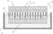
도 8a 및 8c에서 개략적으로 도시된 일 실시예에서, 코팅하는 단계는 액상인 코팅 재료에 의해 코팅 레벨(L1)까지 채워진 탱크(21)를 포함하는 침적 용기(20) 내에서 반제품(15)을 담그는 과정에 의해 발생될 수 있는데, 코팅 재료는 참조 부호 22로 지시된다.In one embodiment, schematically illustrated in Figures 8A and 8C, the coating step includes placing the
코팅 레벨(L1)은 특히 도 8a에 도시된 접촉 헤드(10B)를 포함하거나 도 8c에 도시된 접촉 팁(10A)을 포함하는, 예를 들면, 접촉 프로브들(10)의 단부에 대응되는 반제품(15)의 단지 일 부분, 코팅 필름에 의해 영향을 받는 반제품(15) 및 접촉 프로브들(10)의 부분을 결정한다. 명백하게, 담금(immersion)에 의해 코팅하는 단계는 접촉 프로브들(10)을 포함하는 반제품(15) 전체 또는 부분에 영향을 끼칠 수 있다.The coating level L1 is particularly suitable for the case where the semi-finished product corresponding to the end of the contact probes 10, for example including the
담금에 의해 코팅하는 단계는 전류 없이 구현될 수 있거나 전기 아연 도금 방식일 수 있다.The step of coating by immersion may be implemented without current or it may be an electro galvanizing method.
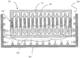
대안적으로, 코팅하는 단계는 기체 상태인 코팅 재료의 도금에 의해 발생할 수 있는데, 특히, 도 8b 및 8d에서 각각 도시되는 바와 같이, 접촉 프로브(10)의 접촉 팁(10A)을 포함하는 단부, 또는 접촉 프로브(10)의 접촉 헤드(10B)를 포함하는 단부에서 도 8b 및 8d에서 개략적으로 도시되는 바와 같이 특히 참조 번호 25로 지시된, 증기 상태인 코팅 재료를 분사하도록 이루어진 하나 이상의 노즐(24)이 설치된 증발 챔버(23) 내에 반제품(15)을 주입하는 것에 의해 발생할 수 있다. 또한, 이 경우에, 증발에 의한 코팅하는 단계는 접촉 프로브들(10)을 전체로서 포함하는 반제품(15) 전체 또는 부분에 영향을 미칠 수 있다. Alternatively, the coating step may occur by plating of the gaseous coating material, and in particular, as shown in Figures 8b and 8d, respectively, an end including the
처리하는 단계가 예를 들면, 각각의 접촉 헤드(10B)를 포함하는 접촉 프로브들(10)의 제1단부에서 반제품(15)을 제1 코팅 단계를 포함하는데 예를 들면 접촉 팁(10A)을 포함하는 접촉 프로브들(10)의 제2단부에서 반제품(15)의 제2 코팅 단계가 이어지고 이 순서대로 또는 반대의 순서대로, 이런 제1 및 제2 코팅 단계가 담금 또는 증발에 의해 구현되는 점이 또한 제공 가능하다. The processing step includes, for example, a first coating step at the first end of the contact probes 10, including each
더욱이, 코팅하는 단계는 음극 스퍼터링 처리에 의해 구현되는 하나 이상의 재료 증착 단계를 포함할 수 있고, 에너지 입자 빔으로 충격이 가해지고 반제품(15)의 표면 상에 재응결될 때 원자, 이온 또는 분자 파편은 타겟으로 불리우는 고체 재료에 의해 배출되고, 반제품(15)이 적절히 충격이 가해진 상기 타겟 코팅 재료와 함께 특수 진공 챔버에 위치될 때 그 안에서 만들어진 접촉 프로브들(10)의 범위의 전체 또는 부분에서 만들어진다. Moreover, the coating step may include one or more material deposition steps implemented by a cathodic sputtering process, and may include atomic, ionic, or molecular debris when impacted by the energy particle beam and recondensed on the surface of the
이런 방식으로, 예를 들면 코팅된 부분이 도 9a에서 참조 부호 14'로 지시된, 접촉 프로브들(10)의 접촉 헤드(10B) 또는 코팅된 부분이 도 9b에서 참조 부호 18'로 지시된, 접촉 프로브들(10)의 접촉 팁(10A)인 하나 이상의 코팅된 부분을 포함하는 반제품(15)은 얻어진다.In this manner, for example, the
도 9c에서 개략적으로 도시된 바와 같이, 접촉 프로브들(10)의 접촉 헤드(10B)에서 제1코팅부(14') 및 접촉 프로브들(10)의 접촉 팁(10A)에서 제2코팅부(18')를 포함하는 반제품(15)을 얻는 것이 또한 가능하다. As shown schematically in Figure 9c, the first coating 14 'at the
더욱이, 전체로서 접촉 프로브들(10)과 같게 실질적으로 연장되는 코팅부를 포함하는 반제품(15)을 얻는 것이 가능하다.Moreover, it is possible to obtain a
반제품(15)이 겪게되는 다른 단계들의 끝에서, 접촉 프로브들(10)은, 바람직하게는 이런 접촉 프로브들(10)을 기판(11)에 고정시키는, 브릿지 재료(13)의 제거 및 약화선(LL)의 파손에 의해 기판(11)으로부터 분리된다.At the end of the other steps that the
하나 이상의 코팅하는 단계를 포함하는 처리하는 단계의 경우, 분리 이후에, 각각이 코팅 필름을 구비하는 하나 이상의 단부를 가지는 복수의 접촉 프로브들(10)이 얻어진다. In the case of a processing step comprising one or more coating steps, after the separation, a plurality of contact probes 10 each having at least one end with a coating film is obtained.
특히, 도 9a에 도시된 종류의 반제품(15)으로부터 시작하여, 도 10a에 개략적으로 도시된 바와 같이, 각각이 접촉 헤드(10B)를 포함하고 코팅부(14')의 코팅 재료로 이루어진 코팅 필름(14A)을 구비하는 하나 이상의 코팅부(14')를 포함하는, 복수의 접촉 프로브들(10)이 얻어진다.In particular, starting with the
일 실시예에서, 접촉 헤드(10B)를 포함하는 단부(14)에서의 코팅 필름(14A)은 구리, 은, 금, 팔라듐 또는 이들의 합금으로부터 선택되거나 그래핀(graphene)으로 이루어진 고 전도성 값을 가지는 코팅 재료로 이루어진다. In one embodiment, the
본 발명의 바람직한 실시예에서, 전도성 코팅 재료는 귀금속 그룹으로부터 선택되되, 보다 바람직하게는 금이다. 이런 방식으로, 접촉 프로브(10)는 단부(14) 및 접촉 패드 사이에서, 예를 들면 도 10a에서 다시 도시되는 비차단 프로브들을 포함하는 테스트 헤드의 경우에 공간 트랜스포머(16)의 접촉 패드(16A) 사이에서 향상된 전기 접속 특성들을 가진다. In a preferred embodiment of the present invention, the conductive coating material is selected from the noble metal group, more preferably gold. In this manner, the
또한 공간 트랜스포머(16)의 접촉 패드(16A)는 차례로 전도성 재료로 이루어지거나 전도성 재료에 의해 코팅될 수 있는데, 전도성 재료는 특히 금속 또는 합금, 보다 구체적으로 접촉 프로브(10)의 접촉 헤드(10B)를 포함하는 단부(14)의 코팅 필름(14A)을 구현하는 같은 재료, 바람직하게는 금일 수 있다. In addition, the
특히 재료가 비커스 스케일에서 500 Hv(4903.5 MPa와 같은) 보다 큰 경도 값을 가지는 코팅 재료의 접촉 헤드(10B)를 포함하는 단부(14)에서 코팅 필름(14A)을 제조하는 것이 유사하게 가능하다. 바람직하게는, 코팅 재료는 팔라듐 또는 니켈-팔라듐과 같은 팔라듐 합금, 구리 및 구리-니오븀 또는 구리-은과 같은 구리 합금, 로듐 및 로듐 합금, 은 또는 금 또는 이들의 합금으로부터 선택되거나 그래핀으로 이루어지거나 도핑된 DLC (“Diamond Like Carbon”)로 이루어진다.It is similarly possible to manufacture the
본 발명의 바람직한 실시예에서, 코팅 재료는 로듐이고, 접촉 프로브(10)는 단부(14), 특히 접촉 헤드(10B)의 향상된 내마모성 특성을 가진다. In a preferred embodiment of the present invention, the coating material is rhodium and the
유사하게는, 도 9b에서 도시된 일례와 같은 반제품(15)으로부터 시작하여, 복수의 접촉 프로브들(10)이 얻어지는데, 도 10b에서 개략적으로 도시되는 바와 같이, 각각의 프로브는 접촉 팁(10A)을 포함하고 코팅부(18')의 코팅 재료로 이루어진 코팅 필름(18A)을 구비하는 하나 이상의 단부(18)를 구비한다. Similarly, a plurality of contact probes 10 are obtained, starting from the
특히, 접촉 팁(10A)을 포함하는 단부(18)에서의 코팅 필름(18A)은 고 전도성 코팅 재료로 이루어질 수 있어서, 접촉 프로브(10)는 단부(18) 및 접촉 패드 사이에서, 예를 들면, 도 10b에 도시되는 바와 같은, 시험 중인 디바이스(17)의 접촉 패드(17A) 사이에서 전기 접속 특성을 향상시킨다. In particular, the
또한, 시험 중인 디바이스(17)의 접촉 패드(17A)는 차례로 전도성 재료로 이루어지거나 전도성 재료, 특히 접촉 프로브(10)의 접촉 팁(10A)을 포함하는 단부(18)의 코팅 필름(18A)을 구현하는 것과 같은 재료에 의해 코팅될 수 있다.The
대안적으로, 접촉 팁(10A)을 포함하는 단부(18)에서의 코팅 필름(18A)은 고 경도를 가지는 코팅 재료를 포함할 수 있고, 따라서 접촉 프로브(10)는 단부(18), 특히 접촉 팁(10A)의 향상된 내마모성 특성을 가진다.Alternatively, the
마지막으로, 도 9c에서 도시되는 일례와 같은 반제품(15)으로부터 시작하여, 복수의 접촉 프로브들(10)을 얻는 것이 또한 가능한데, 도 10c에 개략적으로 도시된 바와 같이, 복수의 접촉 프로브들(10) 각각은 접촉 헤드(10B)를 포함하고 제1코팅부(14')의 코팅 재료로 이루어진 제1 코팅 필름(14A)을 구비하는 제1단부(14) 및 접촉 팁(10A)을 포함하고 제2코팅부(18')의 코팅 재료로 이루어진 제2 코팅 필름(18A)을 구비하는 제2단부(18)를 구비한다. 적절하게는, 이런 제1 및 제2 코팅 필름(14A, 18A)은 같은 코팅 재료 또는 다른 재료로 이루어질 수 있고, 그들은 단일층 또는 다층일 수 있다. Finally, it is also possible to obtain a plurality of contact probes 10, starting from the
도 10c 및 10d 각각에서의 대안적인 실시예들에서와 같은 단부들(14, 18)에서와 같거나 다른 형상 및 치수를 가지는 접촉 프로브들(10)을 고려하는 것이 또한 가능하다. It is also possible to consider the contact probes 10 having the same or different shape and dimensions as at the
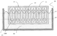
더욱이, 본 발명에 의하면 유리하게는, 접촉 프로브들(10)의 중앙부(19A)에서 하나 이상의 덮는 필름(19)을 제공하기 위해, 복수의 접촉 프로브들(10)을 포함하는 반제품(15)의 제조방법은 반제품(15)의 하나 이상의 부분의 유전성 덮는 재료에 의한 덮는 단계를 포함하고 용어 중앙부는, 도 11a 및 11b에서 개략적으로 도시되는 바와 같이, 접촉 팁(10A) 및 접촉 헤드(10B) 모두를 포함하지 않는 부분을 의미한다.Moreover, according to the present invention, it is advantageous to provide a
적절하게는, 덮는 필름(19)은, 특히 플루오르화 폴리머, 폴리(p-자일릴렌) 폴리머, 바람직하게는 특히 C 타입 또는 F 타입의 패럴린®, 그것의 공중합체 또는 나노복합체 또는 도핑되지 않은 DLC("Diamond Like Carbon"), 바람직하게는 C 타입 또는 F 타입의 패럴린®으로부터 선택된 유전성 재료로 이루어진다. Suitably, the covering
보다 구체적으로, 덮는 단계는 재료를 덮고 이어지는 반제품(15)의 마스킹, 및 접촉 프로브들(10)의 관심 부분 밖에서 덮는 재료를 제거하는 것에 의해 전체를 덮는 단계를 포함할 수 있고, 따라서, 예를 들면 중앙부(19A)과 같은 관심 부분에서만 덮는 필름(19)을 구현한다. 특히, 도 11a에 개략적으로 도시되는 바와 같이, 접촉 프로브들(10)의 중앙부(19A)에서 연장된 반제품(15)의 밴드를 덮는 직사각형의 마스크를 실질적으로 적용할 때, 덮는 필름(19)에 의해 덮여진 각각의 중앙부(19A)을 가지는 복수의 접촉 프로브들(10)을 구비하는 반제품(15)은 따라서 이렇게 얻어진다. 이런 경우에, 덮는 필름(19)의 부분들(19B)은 접촉 프로브들(10)을 둘러쌓는 프레임들(12)에서 기판(11)의 중앙부에 또한 남겨진다. More specifically, the covering step may include covering the entire material by covering the material, masking the subsequent
대안적으로, 도 11b에 개략?Ю막? 도시되는 바와 같이, 접촉 프로브들(10)의 중앙부(19A)만을 덮개를 벗긴 채로 남겨두기 위해, 특히 그물모양과 같은 보다 복잡한 마스크를 사용하는 것이 가능하다.Alternatively, as shown in Fig. 11B, As shown, it is possible to use a more complex mask, such as a mesh, in particular, to leave only the
제한되지 않는 예에 의해서, 덮는 단계는 화학 증착(CVD, chemical vapor deposition) 단계 또는 피막 보호(passivation)를 포함한다. By way of non-limiting example, the covering step includes a chemical vapor deposition (CVD) step or passivation.
모든 프로브들에 영향을 끼치는 처리하는 단계가 덮는 필름(19)을 구현하도록 의도되는 덮는 단계를 포함하도록 제공하는 것이 또한 가능하다.It is also possible to provide a processing step that affects all probes, including a covering step intended to embody the covering
이 경우에, 본 발명에 의하면 유리하게는, 처리하는 단계는 반제품(15)의 하나 이상의 부분, 특히 접촉 프로브들(10)의 중앙부(19A)에 대응되는 부분을 코팅하는 하나 이상의 단계를 포함할 수 있는데 덮는 필름(19)을 포함하는 코팅된 중앙부(19')을 구현하기에 적합한 유전체의 덮는 재료로 코팅한다.In this case, advantageously according to the invention, the treating step comprises one or more steps of coating at least one part of the
편리하게는, 유전체 덮는 재료로 코팅하는 단계는 담금 욕조(20)의 탱크(21)를 이용하되 26으로 보여지는 액상인 유전체의 덮는 재료에서 적절한 덮는 마스크를 갖는 반제품(15)을 담그는 단계를 포함할 수 있다. Conveniently, the step of coating with a dielectric covering material comprises immersing the
이 경우에, 접촉 프로브들(10)의 중앙부(19A)이 상부 코팅 레벨(L2)에서부터 하부 코팅 레벨(L3)까지 연장되고, 도 12a에 개략적으로 도시되는 바와 같이 액상의 유전성의 덮는 재료(26)는 탱크(21)에서 적어도 상부 코팅 레벨(L2)에 도달해야 한다.In this case, the
앞서 도시된 바와 같이, 반제품(15)은 접촉 프로브들(10)의 중앙부(19A) 밖에서 즉, 적어도 상부 코팅 레벨(L2) 보다 위이며 하부 코팅 레벨(L3) 보다 아래에서 연장되는 덮는 마스크를 포함할 수 있다. The
대안적으로, 유전성의 덮는 재료로 코팅하는 단계는 원하는 하부 코팅 레벨(L3) 아래의 덮는 필름(19)을 제거하는 단계를 뒤따르는 원하는 상부 코팅 레벨(L2)에 도달하는 액상의(26) 유전성인 덮는 재료에서 반제품(15)을 담그는 단계를 포함할 수 있다. Alternatively, the step of coating with a dielectric covering material may include removing the covering film (19) below the desired lower coating level (L3) and removing the covering film (19) below the desired lower coating level (L3) And dipping the
원하는 하부 코팅 레벨(L3) 아래이고 원하는 상부 코팅 레벨(L2)을 넘는 덮는 필름(19)을 제거하는 단계에 뒤따르는 액상인 유전성의 덮는 재료(26)에서 반제품(15)을 완전히 담그는 단계를 포함하는 유전성의 덮는 재료로 코팅하는 단계를 고려하는 것이 또한 가능하다. A dielectric
편리하게는, 덮는 필름(19)을 제거하는 단계는 화학적 에칭에 의해 발생할 수 있고, 반제품(15)에 적용되는 적절한 마스크의 사용에 의해 가능하다.Conveniently, the step of removing the covering
도 12b에 개략적으로 도시되는 바와 같이, 접촉 프로브들(10)의 중앙부(19A)에서 반제품(15)의 코팅된 중앙부(19A)를 구현하기 위해, 27로 도시되는 증기상인 유전성의 덮는 재료를 분사하도록, 증발 챔버(23)를 사용하는 것이 또한 가능하다.To embody the coated
적절하게는, 이 경우에는 상부 코팅 레벨(L2) 및 하부 코팅 레벨(L3) 사이에서 포함된 증발 챔버(23)의 노즐(24)만이 동작되는데, 노즐은 덮는 필름(19)에 의해 덮혀진 중앙부(19A)의 연장에 대응된다. Suitably, in this case, only the
전술한 담금에 의한 코팅하는 단계에 관하여, 증발을 사용함으로써 접촉 프로브들(10)의 중앙부(19A)를 포함하는 반제품(15)의 부분에서만 덮는 필름(19)을 구현하는 것은 완전히 가능하여서 코팅부(19')를 구현하고 이로 인해 반제품(15)으로 마스크를 적용하고 제거하는 것을 피하게 할 수 있다는 점이 강조되어야 한다. With respect to the coating step with the above-mentioned dipping, it is entirely possible to realize the
이런 경우에, 덮는 필름(19)의 부분(19B)은, 도 13에서 개략적으로 도시되는 바와 같이 프레임(12)에서 기판(11) 상에 남겨질 수 있는데, 코팅부(19')는 모든 반제품(15)을 따라서 연장되는데; 이런 부분(19B)은 어떤 유용함도 가질 수 없으며, 본 발명에 의한 반제품(15)으로부터 얻어진 접촉 프로브들(10)의 구성이나 성능에 어떠한 영향을 주지도 않는다는 점이 강조되어야 한다. In this case, the
실제로, 접촉 프로브들(10)이 반제품(15)으로부터 분리된 후에, 이런 부분(19B)은 접촉 프로브들(10)을 제외하는 기판(11)과 함께 제거될 것인데, 브릿지 재료(13)도 가능하다.In practice, after the contact probes 10 are separated from the
코팅 중앙부(19')를 구비하고 하나 이상의 부분, 특히 접촉 프로브들(10)의 중앙부(19A)에 배치되는 반제품(15)을 제공하는 경우, 이후의 어느 처리 단계는 덮는 필름(19)을 기준 또는 "스토퍼"로서 또한 사용할 수 있다. In the case of providing a
특히, 접촉 프로브들(10)의 단부를 연속적으로 코팅하는 단계의 경우, 코팅 중앙부(19')의 존재는 완전히 또는 상당히 코팅 재료의 부착을 방지할 수 있는 덮는 재료가 선택되도록 제공되는 코팅 재료에 의해 코팅될 단부의 추측의 치수를 결정을 허용하다. In particular, in the case of the step of continuously coating the ends of the contact probes 10, the presence of the coating central portion 19 ' is sufficient to completely or substantially prevent coating of the coating material, Allow the determination of the dimensions of the specimen to be coated by the end.
앞서 설명한 바와 같이, 비 제한적인 예에 의해서, 하나 이상의 코팅 중앙부(19')를 포함하는 반제품(15)의 제조방법은 특히, 금속 재료 또는 합금, 바람직하게는 금인 코팅 재료에 의한 접촉 프로브들(10)의 일단부 또는 양단부(14 및 18)를 코팅하는 하나 이상의 단계를 포함하는 점이 고려되는 것이 가능한데, 이는 도 14a 및 14b에서 개략적으로 도시되는 바와 같이, 반제품(15)이 접촉 헤드(10B) 및 접촉 팁(10A)에서 각각 담그어지는 액상인 코팅 재료(22)에서의 반제품(15)의 담금에 의해, 또는 도 14c 및 14d에서 개략적으로 도시되는 바와 같이, 반제품(15)이 접촉 헤드(10B) 및 접촉 팁(10A)에서 각각 증발되는 증발 챔버(23)에서의 반제품(15)의 삽입에 의해 이루어진다.As described above, by way of non-limiting example, the method of manufacturing the
이런 방식으로, 코팅 중앙부(19') 및 하나 이상의 추가의 코팅부, 예를 들면 부분이 도 15a에서 참조 부호 14'로 지시되는, 접촉 프로브들(10)의 접촉 헤드(10B) 또는 부분이 도 15b에서 참조 부호 18'로 지시되는, 접촉 프로브들(10)의 접촉 팁(10A)를 포함하는 반제품(15)이 얻어진다. In this manner, the
도 15c에서 개략적으로 도시된 바와 같이, 코팅 중앙부(19') 및 접촉 프로브들(10)의 접촉 헤드(10B)에서의 추가의 제1코팅부(14')와 접촉 프로브들(10)의 접촉 팁(10A)에서의 추가의 제2코팅부(18')를 포함하는 반제품(15)을 얻는 것이 또한 가능하다.The contact of the contact probes 10 with the additional first coating portion 14 'in the
그 결과, 본 발명에 의한 제조방법은 코팅하는 단계가 반제품(15)의 하나 이상의 코팅부(14', 18', 19')에서 코팅 필름을 구현하는 것, 그리고 하나 이상의 코팅부(14', 18')는, 반제품(15)에서 구현된 접촉 프로브들(10)의 접촉 팁(10A) 또는 접촉 헤드(10B)를 포함하는 반제품(15)의 단부에 배치되고 및/또는 하나 이상의 코팅부(19')는, 반제품(15)에서 구현된 접촉 프로브들(10)의 접촉 팁(10A) 및 접촉 헤드(10B) 모두를 포함하지 않는 반제품(15)의 중앙부에 배치되는 것을 제공한다. As a result, the manufacturing method according to the present invention is characterized in that the coating step implements a coating film on one or more coatings 14 ', 18', 19 'of the
더욱이, 전체로서 접촉 프로브들(10)과 같이 실질적으로 연장된 코팅부를 포함하는 반제품(15)을 얻는 것이 가능하다. Moreover, it is possible to obtain a
형성하는 단계는, 바람직하게 상기 접촉 프로브(10)의 접촉 팁(10A)을 포함하는 제1단부에 대응되는, 중앙 위치에 위치된 하나 이상의 제1 브릿지 재료(13) 및 바람직하게 접촉 프로브(10)의 접촉 헤드(10B)를 포함하는 제2단부에 대응되는 측면 위치에 위치된 하나의 제2 브릿지 재료(13)를 포함하는 접촉 프로브들(10) 각각을 구현하는 것이 또한 강조된다. The forming step preferably comprises at least one
아울러, 형성하는 단계는, 브릿지 재료(13) 각각에 그것을 통과하고 상기 브릿지 재료(13)의 무결성을 파손하도록 기판(11)으로부터 접촉 프로브(10)의 분리를 가능하게 이루어지는 하나 이상의 약화선(LL)을 장착하는 단계를 더 포함하고, 하나 이상의 약화선(LL)은 상기 반제품(15)의 평면과 수직 방향을 따라서, 상기 기판(11)의 대응되는 국부 세선(local thinning)에 의해 얻어진다. In addition, the forming step includes the step of providing at least one weakening line LL (not shown) that enables separation of the
반제품(15)이 겪게되는 다른 단계들의 종료 시점에 접촉 프로브(10)는 그 후에 바람직하게 약화선(LL)의 파손 및 이런 접촉 프로브(10)를 기판(11)에 고정하는, 브릿지 재료(13)의 제거에 의해, 기판(11)으로부터 분리된다. At the end of the other steps that the
도 16a 내지 16c에 개략적으로 도시되는 바와 같이, 분리 단계 이후에, 복수의 접촉 프로브들(10)이 얻어지는 경우에, 각각의 프로브는 코팅 재료에 의해 코팅된 하나 또는 양 단부를 구비하고 덮는 재료(19)에 의해 코팅된 중앙부(19A)에 인접한다. 16A to 16C, after the separation step, when a plurality of contact probes 10 are obtained, each probe has one or both ends coated with a coating material, 19 adjacent to the
결론적으로, 본 발명은 테스트 헤드용 복수의 접촉 프로브들(10)을 포함하는 반제품(15)을 제공하는데, 각각의 이런 접촉 프로브들(10)은 전도성 재료의 기판(11)에서 구현되고 하나 이상의 브릿지 재료(13)에 의해 기판(11)에 고정된다. In conclusion, the present invention provides a
그들이 얻어진 박층에서 프로브들의 고정 및 전체 제조처리의 마지막에서만 박층으로부터 접촉 프로브들을 분리시키기 시작하는 것으로 인해 본 발명에 의한 반제품은 전체로서 내부에서 구현된 접촉 프로브들의 덮는 동작 및/또는 코팅을 수행하는 것을 허용한다. By starting to separate the contact probes from the thin layer only at the end of the fixation and overall manufacturing process of the probes in the thin layer from which they are obtained, the semi-finished product according to the invention is able to perform the covering operation and / Allow.
유리하게는, 반제품은 기판으로부터 재료를 제거하는 것에 의해 형성된 복수의 접촉 프로브들을 형성하는 하나 이상의 단계를 포함하는 방법에 의해 얻어지는데, 프로브들은 서로 같거나 다른 어느 형상일 수 있고, 각각의 접촉 프로브는 하나 이상의 브릿지 재료를 구비한다. 형성하는 단계는 치수적인 구속조건을 감소시키고 고 정밀 수준인 레이저 커팅에 의해 극도록 효율적인 방식으로 수행되는데, 이런 특징은 프로브들 및 브릿지 재료를 위한 관련된 치수를 고려하면 특히 유리하다. 형성하는 단계는 특히 반제품의 평면에 수직 방향으로 약화선들에서 이런 브릿지 재료의 두께를 얇게하는 것에 의해 브릿지 재료의 약화선을 형성하는 것을 또한 허용한다.Advantageously, the semi-finished product is obtained by a method comprising at least one step of forming a plurality of contact probes formed by removing material from the substrate, wherein the probes may be of the same or different shape, Has at least one bridge material. The forming step is performed in a highly efficient manner by reducing the dimensional constraints and by laser cutting at a high precision level, which is particularly advantageous when considering the relative dimensions for the probes and the bridge material. The forming step also allows the weakening of the bridge material to be formed by thinning the thickness of such bridging material, especially at weakened lines in a direction perpendicular to the plane of the semi-finished product.
적절하게는, 본 발명에 의한 반제품의 제조방법의 코팅하는 단계는 액상인 코팅 재료에서의 담금 및 기상인 코팅 재료의 증발에 의해 구현될 때 요구되는 코팅 재료의 최소 공급을 감소시키는 것을 또한 허용하고, 접촉 프로브들 및 반제품의 최종 비용에서 명백히 유리한 결론이 얻어지는데, 하지만 이런 코팅 재료들은 매우 고가이다.Suitably, the coating of the method of making a semi-finished product according to the present invention also allows to reduce the minimum supply of coating material required when embodied in a liquid phase coating material and evaporation of the gaseous phase coating material , Contact probes and semi-finished products, but these coating materials are very expensive.
반제품을 특히 유전성이고, 다음의 또한 코팅 단계를 위해 스토퍼로서 동작할 수 있는 덮는 필름, 특히 전도성의 코팅 필름으로 덮는 것이 또한 가능한데, 전도성의 코팅 필름은 귀금속들로 이루어진 전도체의 경우 또는 매우 고가의 재료의 경우에 특히 유리하다. It is also possible to cover the semi-finished product with a covering film, in particular a conductive coating film, which is particularly dielectric and which can also act as a stopper for the subsequent coating step, in the case of a conductor made of noble metals or a very expensive material Particularly in the case of < / RTI >
명백하게는, 전술한 제조방법 및 반제품으로, 특정 요구를 만족하는 목적 및 본 명세서와 함께, 당업자는 다음의 청구항들에 의해 정의되는 본 발명의 보호 범위 내에 모두 포함된 몇몇의 변형 및 수정을 수행할 수 있다.Obviously, those skilled in the art will readily appreciate that many modifications and variations are possible in the manner of the above described methods of manufacture and semi-finished products, objects of satisfying particular needs, and the present disclosure, including all such modifications as fall within the scope of protection of the present invention as defined by the following claims. .
Claims (17)
- 전도성 재료로 이루어진 기판(11)을 제공하는 단계; 및
- 하나 이상의 브릿지 재료(13)에 의해 상기 접촉 프로브들(10) 각각이 상기 기판(11)에 고정되도록 상기 기판(11)으로부터 재료를 제거함으로써 상기 접촉 프로브들(10) 각각을 형성하는 단계를 포함하고,
상기 접촉 프로브들(10)을 형성하는 단계는, 상기 접촉 프로브들(10) 및 상기 하나 이상의 브릿지 재료(13)의 형태에 대응한 레이저 커팅 단계를 포함하는 반제품(15)의 제조방법.A method of manufacturing a semi-finished product (15) comprising a plurality of contact probes (10) for a test head of electronic devices,
- providing a substrate (11) made of a conductive material; And
- forming each of the contact probes (10) by removing material from the substrate (11) so that each of the contact probes (10) is secured to the substrate (11) by one or more bridging materials Including,
Wherein forming the contact probes (10) comprises laser cutting corresponding to the shapes of the contact probes (10) and the one or more bridge materials (13).
상기 접촉 프로브들(10)을 형성하는 단계는, 상기 기판(11)을 마스킹하고 에칭하는 하나 이상의 단계 또는 상기 기판(11)을 선택적으로 화학적 에칭하는 단계를 선택적으로 포함하는, 상기 기판(11)의 마스킹 처리 및 후속의 화학적 에칭에 의한 포토리소그래피 에칭 단계를 포함하는 것을 특징으로 하는 반제품(15)의 제조방법.The method according to claim 1,
The step of forming the contact probes 10 further comprises selectively etching the substrate 11 or one or more steps of masking and etching the substrate 11, And a photolithographic etching step by a subsequent chemical etching process.
상기 형성하는 단계는, 상기 접촉 프로브들(10) 각각을 따라서, 대칭 또는 비대칭의, 완전히 임의적인 방식으로 위치되고, 복수의 브릿지 재료(13) 각각에 의해 상기 기판(11)에 고정된 상기 접촉 프로브들(10)을 구현하는 것을 특징으로 하는 반제품(15)의 제조방법.3. The method according to claim 1 or 2,
Wherein said forming comprises positioning said contact probes in a substantially symmetrical or asymmetrical manner along each of said contact probes, Characterized in that it implements the probes (10).
상기 형성하는 단계는, 바람직하게 상기 접촉 프로브들(10)의 접촉 팁(10A)을 포함하는 제1단부에 대응되는, 중앙 위치에 위치된 하나 이상의 제1 브릿지 재료(13) 및 바람직하게 상기 접촉 프로브(10)의 접촉 헤드(10B)를 포함하는 제2단부에 대응되는 측면 위치에 위치된 하나의 제2 브릿지 재료(13)를 포함하는 상기 접촉 프로브들(10) 각각을 구현하는 것을 특징으로 하는 반제품(15)의 제조방법.4. The method according to any one of claims 1 to 3,
The forming step preferably comprises providing at least one first bridge material (13) located at a central position, corresponding to a first end comprising a contact tip (10A) of the contact probes (10) Each of the contact probes 10 comprising one second bridge material 13 located at a lateral position corresponding to a second end comprising the contact head 10B of the probe 10 (15).
상기 형성하는 단계는, 상기 브릿지 재료(13) 각각에 그것을 통과하고 상기 브릿지 재료(13)의 무결성을 파손하도록 상기 기판(11)으로부터 상기 접촉 프로브(10)의 분리를 가능하게 이루어지는 하나 이상의 약화선(LL)을 장착하는 단계를 더 포함하고,
상기 하나 이상의 약화선(LL)은 상기 반제품(15)의 평면에 수직인 방향을 따라서, 상기 기판(11)의 대응되는 국부 세선에 의해 얻어지는 것을 특징으로 하는 반제품(15)의 제조방법.5. The method according to any one of claims 1 to 4,
Wherein said forming step includes the step of providing a plurality of bridging materials (13) each having at least one weakening line (13) that is capable of separating said contact probe (10) from said substrate (11) (LL), the method comprising:
Characterized in that said at least one weakening line (LL) is obtained by a corresponding local fine line of said substrate (11) along a direction perpendicular to the plane of said semi-finished product (15).
상기 기판(11)을 제공하는 단계는,
- 전도성 재료로 이루어진 단일층을 제공하는 단계; 또는
- 전도성 재료로 이루어진 하나 이상의 코팅층에 의해 덮여진 제1 전도성 재료로 이루어진 중앙층 또는 코어(11A)를 포함하고, 상기 기판(11)에서 구현된 상기 접촉 프로브들(10)의 경도에 대한 성능 및/또는 전자 기계 성능을 향상시키기에 적합한 다층을 제공하는 단계 중 하나를 포함하는 것을 특징으로 하는 반제품(15)의 제조방법.6. The method according to any one of claims 1 to 5,
The step of providing the substrate (11)
Providing a single layer of conductive material; or
- a central layer or core (11A) of a first conductive material covered by at least one coating layer of conductive material, characterized in that the performance of the contact probes (10) implemented in the substrate (11) And / or providing a multi-layer suitable for improving electromechanical performance. ≪ Desc / Clms Page number 20 >
코팅 단계, 덮는 단계, 레이저, 포토리소그래피 또는 전기 아연 도금 형성 단계, 전기 도금 단계, 전기 아연 도금 증착 단계, 정밀기계 처리 단계, 스퍼터링 단계, 화학적 또는 물리적 에칭 단계로부터 선택된 하나 이상의 단계를 포함하는, 상기 반제품(15)에 포함된 상기 접촉 프로브들(10) 모두와 관련된 하나 이상의 처리 단계를 포함하는 것을 특징으로 하는 반제품(15)의 제조방법.7. The method according to any one of claims 1 to 6,
Comprising at least one step selected from a coating step, a covering step, a laser, a photolithography or electro-galvanizing step, an electroplating step, an electro-galvanizing deposition step, a precision machining step, a sputtering step, Characterized in that it comprises at least one processing step associated with all of said contact probes (10) contained in the semi-finished product (15).
상기 처리 단계는 전체적으로 모든 상기 접촉 프로브들(10) 또는 상기 접촉 프로브들(10)의 하나 이상의 부분에 영향을 미치는 것을 특징으로 하는 반제품(15)의 제조방법.8. The method of claim 7,
Wherein said processing step generally affects at least one part of all said contact probes (10) or said contact probes (10).
상기 처리 단계는 상기 반제품(15)의 같거나 다른 부분들을 위한 같은 종류의 다수의 반복되는 단계들을 포함하는 것을 특징으로 하는 반제품(15)의 제조방법.9. The method according to claim 7 or 8,
Characterized in that the processing step comprises a number of repeated steps of the same kind for the same or different parts of the semi-finished product (15).
상기 처리 단계는 전도성 재료 및 유전성 재료로부터 선택된 코팅 재료로 이루어진 코팅 필름의 구현으로 하나 이상의 상기 반제품(15) 및 상기 접촉 프로브들(10) 또는 그것의 일부분을 코팅하는 하나 이상의 단계를 포함하는 것을 특징으로 하는 반제품(15)의 제조방법.10. The method according to any one of claims 7 to 9,
Characterized in that said processing step comprises one or more steps of coating one or more of said semi-finished products (15) and said contact probes (10) or a part thereof in the implementation of a coating film consisting of a coating material selected from a conductive material and a dielectric material (15).
상기 코팅하는 단계는 상기 반제품(15)의 하나 이상의 코팅부(14', 18', 19') 상에 상기 코팅 필름을 구현하고, 상기 하나 이상의 코팅부(14', 18')는 상기 반제품(15)에서 구현된 상기 접촉 프로브들(10)의 접촉 팁(10A) 또는 접촉 헤드(10B)를 포함하는 부분을 의미하는 상기 반제품(15)의 단부에 배치되고, 및/또는 상기 하나 이상의 코팅부(19')는 상기 반제품(15)에서 구현된 상기 접촉 프로브들(10)의 접촉 팁(10A) 및 접촉 헤드(10B)를 포함하지 않는 부분을 의미하는 상기 반제품(15)의 중앙부에 배치되는 것을 특징으로 하는 반제품(15)의 제조방법.11. The method of claim 10,
Wherein the coating step implements the coating film on at least one coating part (14 ', 18', 19 ') of the semi-finished product (15) and the at least one coating part (14', 18 ' Which is disposed at an end of the semi-finished product 15, which means a portion including the contact tip 10A or the contact head 10B of the contact probes 10 implemented in the one or more coatings 15 and / (19 ') is disposed at a central portion of the semi-finished product (15), which means a portion not including the contact tip (10A) and the contact head (10B) of the contact probes (10) implemented in the semi-finished product (15). ≪ / RTI >
상기 코팅하는 단계는 팔라듐 또는 니켈-팔라듐과 같은 팔라듐 합금, 구리, 및 구리- 니오븀 또는 구리-은과 같은 구리 합금, 로듐 및 로듐의 합금, 은 또는 금이나 이들의 합금들로부터 선택된 금속 또는 합금으로 이루어지거나, 또는 그래핀으로 이루어지거나, 또는 도핑된 DLC ("Diamond Like Carbon")로 이루어지고, 바람직하게는 귀금속들의 그룹으로부터 선택되거나, 보다 바람직하게는 금으로 이루어진 전도성 재료의 상기 코팅 필름을 구현하는 것을 특징으로 하는 반제품(15)의 제조방법.The method according to claim 10 or 11,
The coating may be carried out using a palladium alloy such as palladium or nickel-palladium, copper and copper alloys such as copper-niobium or copper-silver, alloys of rhodium and rhodium, metals or alloys selected from silver or gold or alloys thereof (DLC) ("Diamond Like Carbon"), preferably made from a group of precious metals, or more preferably made of gold, (15). ≪ / RTI >
상기 코팅하는 단계는 플루오르화 폴리머, 폴리(p-자일릴렌) 폴리머, 바람직하게는 특히 C 타입 또는 F 타입의 패럴린®, 그것의 공중합체 또는 나노복합체 또는 도핑되지 않은 DLC("Diamond Like Carbon"), 바람직하게는 C 타입 또는 F 타입의 패럴린®으로부터 선택된 유전성 재료의 상기 코팅 필름을 구현하는 것을 특징으로 하는 반제품(15)의 제조방법.The method according to claim 10 or 11,
The coating may be carried out using a fluoropolymer, a poly (p-xylylene) polymer, preferably a C or F type paralel®, a copolymer or nanocomposite thereof or an undoped DLC ("Diamond Like Carbon" ), Preferably a C type or an F type paralel (R). ≪ / RTI >
상기 코팅하는 단계는:
- 침적 용기(20)의 탱크(21) 내의 액상(22)인 코팅 재료에서 상기 반제품(15)을 담그고, 상기 액상인 코팅 재료(22)는 상기 탱크(21)를 상기 코팅 필름에 의해 코팅된 상기 반제품(15)의 부분을 결정하도록 이루어지는 코팅 레벨(L1)까지 채우는 과정; 또는
- 상기 코팅 필름에 의해 코팅된 상기 반제품(15)의 하나 이상의 부분에 대응되는 증기상인 코팅 재료(25)를 분사하도록 이루어진 하나 이상의 노즐(24)이 장착된, 증발 챔버(23)에서 상기 반제품(15)의 삽입하는 과정으로부터 선택된 것을 특징으로 하는 반제품(15)의 제조방법.14. The method according to any one of claims 10 to 13,
Wherein the coating step comprises:
- immersing the semi-finished product (15) in a coating material which is a liquid phase (22) in a tank (21) of a dipping vessel (20), said liquid phase coating material (22) Filling up the coating level L1 to determine a portion of the semi-finished product 15; or
In the evaporation chamber (23), equipped with at least one nozzle (24) adapted to spray a coating material (25) which is a vapor phase corresponding to at least one part of said semi-finished product (15) coated by said coating film 15. The method of producing a semi-finished product according to claim 1,
상기 코팅하는 단계는 음극 스퍼터링 처리에 의해 구현되는 하나 이상의 재료 증착 단계를 포함하고, 에너지 입자 빔으로 충격이 가해지고 상기 반제품(15)의 표면 상에 재응결될 때 원자, 이온 또는 분자 파편은 타겟으로 불리우는 고체 재료에 의해 배출되고, 상기 반제품(15)이 적절히 충격이 가해진 상기 타겟 코팅 재료와 함께 특수 진공 챔버에 위치될 때 그 안에서 만들어진 상기 접촉 프로브들(10)의 범위의 전체 또는 부분에서 만들어지는 것을 특징으로 하는 반제품(15)의 제조방법.14. The method according to any one of claims 10 to 13,
The coating step comprises at least one material deposition step implemented by a cathodic sputtering process, wherein atomic, ionic or molecular debris, when impacted by the energy particle beam and recondensed on the surface of the semi-finished product (15) (15) is made in all or part of the range of contact probes (10) made therein when placed in a special vacuum chamber with the suitably impacted target coating material (15). ≪ / RTI >
상기 반제품(15)의 부분, 바람직하게는, 상기 접촉 팁(10A) 및 상기 접촉 헤드(10B) 모두를 포함하지 않는 것을 의미하는 부분인 상기 접촉 프로브들(10)의 중앙부(19A)에 대응되는 부분에서 하나 이상의 덮는 필름(19)을 구현하도록 상기 반제품(15)의 하나 이상의 부분의 유전성의 덮는 재료에 의해 덮는 단계를 더 포함하는 것을 특징으로 하는 반제품(15)의 제조방법.16. The method according to any one of claims 1 to 15,
Corresponds to the central portion 19A of the contact probes 10 which is a portion of the semi-finished product 15, preferably a portion which does not include both the contact tip 10A and the contact head 10B Characterized in that the method further comprises the step of covering with at least one part of the at least one part of the semi-finished product (15) with a dielectric covering material so as to realize at least one covering film (19).
Priority Applications (1)
| Application Number | Priority Date | Filing Date | Title |
|---|---|---|---|
| KR1020237002987A KR20230019226A (en) | 2014-12-30 | 2015-12-18 | Semi-finished product comprising a plurality of contact probes for a testing head and related manufacturing method |
Applications Claiming Priority (3)
| Application Number | Priority Date | Filing Date | Title |
|---|---|---|---|
| ITMI20142287 | 2014-12-30 | ||
| ITMI2014A002287 | 2014-12-30 | ||
| PCT/EP2015/080419 WO2016107756A1 (en) | 2014-12-30 | 2015-12-18 | Semi-finished product comprising a plurality of contact probes for a testing head and related manufacturing method |
Related Child Applications (1)
| Application Number | Title | Priority Date | Filing Date |
|---|---|---|---|
| KR1020237002987A Division KR20230019226A (en) | 2014-12-30 | 2015-12-18 | Semi-finished product comprising a plurality of contact probes for a testing head and related manufacturing method |
Publications (1)
| Publication Number | Publication Date |
|---|---|
| KR20170105030A true KR20170105030A (en) | 2017-09-18 |
Family
ID=52633393
Family Applications (2)
| Application Number | Title | Priority Date | Filing Date |
|---|---|---|---|
| KR1020237002987A KR20230019226A (en) | 2014-12-30 | 2015-12-18 | Semi-finished product comprising a plurality of contact probes for a testing head and related manufacturing method |
| KR1020177021260A KR20170105030A (en) | 2014-12-30 | 2015-12-18 | Semi-finished products including contact probes for a plurality of test heads and a method for manufacturing the same |
Family Applications Before (1)
| Application Number | Title | Priority Date | Filing Date |
|---|---|---|---|
| KR1020237002987A KR20230019226A (en) | 2014-12-30 | 2015-12-18 | Semi-finished product comprising a plurality of contact probes for a testing head and related manufacturing method |
Country Status (9)
| Country | Link |
|---|---|
| US (1) | US10365299B2 (en) |
| EP (1) | EP3241029B1 (en) |
| JP (1) | JP2018508753A (en) |
| KR (2) | KR20230019226A (en) |
| CN (2) | CN107667295A (en) |
| PH (1) | PH12017501219A1 (en) |
| SG (1) | SG11201704481PA (en) |
| TW (1) | TWI705249B (en) |
| WO (1) | WO2016107756A1 (en) |
Cited By (4)
| Publication number | Priority date | Publication date | Assignee | Title |
|---|---|---|---|---|
| KR102021846B1 (en) * | 2019-05-29 | 2019-09-17 | 대경에스티 주식회사 | Manufacturing method of a socket for inspecting an IC chip having an excellent anti-abrasive property and its release |
| KR102068699B1 (en) * | 2018-08-24 | 2020-01-21 | 주식회사 에스디에이 | Manufacturing method of MEMS probe for inspecting semiconductor by using laser |
| KR20200106305A (en) * | 2019-03-04 | 2020-09-14 | (주)디팜스테크 | A contact pin for a semiconductor socket which can form a pre-ionized plating part and enhance reliability |
| WO2022164173A1 (en) * | 2021-01-29 | 2022-08-04 | (주)포인트엔지니어링 | Electro-conductive contact pin, manufacturing method therefor, and electro-conductive contact pin module |
Families Citing this family (11)
| Publication number | Priority date | Publication date | Assignee | Title |
|---|---|---|---|---|
| JP2018506030A (en) * | 2014-12-30 | 2018-03-01 | テクノプローベ エス.ピー.エー. | Method for manufacturing a contact probe for a test head |
| IT201600127507A1 (en) * | 2016-12-16 | 2018-06-16 | Technoprobe Spa | Contact probe and relative measuring head for an electronic device test device |
| TWI629485B (en) * | 2017-05-19 | 2018-07-11 | 中華精測科技股份有限公司 | Probe for probe card and manufacturing method thereof |
| TWI787302B (en) * | 2017-07-10 | 2022-12-21 | 日商聯合精密科技股份有限公司 | Method for manufacturing binary copper-silver alloy body, contact pin and device using binary copper-silver alloy |
| CN110068711B (en) * | 2018-01-24 | 2022-04-26 | 台湾中华精测科技股份有限公司 | Probe card device and rectangular probe |
| TWI638166B (en) * | 2018-01-24 | 2018-10-11 | 中華精測科技股份有限公司 | Probe card device and rectangular probe |
| IT201800005444A1 (en) * | 2018-05-16 | 2019-11-16 | Measurement board with high performance in high frequency | |
| CN109633225A (en) * | 2018-12-27 | 2019-04-16 | 深圳市海维光电科技有限公司 | A kind of production technology of circuit board detecting testing needle |
| JP2021076486A (en) * | 2019-11-11 | 2021-05-20 | 株式会社日本マイクロニクス | Electrical connection device |
| KR102456469B1 (en) * | 2020-08-11 | 2022-10-21 | 리노공업주식회사 | Method and Device for fabricating the test probe |
| CN115932425A (en) * | 2021-08-24 | 2023-04-07 | 三赢科技(深圳)有限公司 | Test method of electronic product, electronic device and storage medium |
Family Cites Families (27)
| Publication number | Priority date | Publication date | Assignee | Title |
|---|---|---|---|---|
| JPH01287484A (en) * | 1988-05-16 | 1989-11-20 | Hitachi Ltd | Probe head and its manufacture and semiconductor lsi inspecting device using same |
| JPH05322930A (en) * | 1992-05-15 | 1993-12-07 | Nippon Maikuronikusu:Kk | Probe assembly and manufacture thereof |
| US6690186B2 (en) * | 1994-07-07 | 2004-02-10 | Tessera, Inc. | Methods and structures for electronic probing arrays |
| US5557214A (en) * | 1995-02-06 | 1996-09-17 | Barnett; C. Kenneth | Micro beam probe semiconductor test interface |
| JPH09126833A (en) * | 1995-10-31 | 1997-05-16 | Olympus Optical Co Ltd | Beam structure of amorphous alloy and its manufacturing method |
| US5667410A (en) * | 1995-11-21 | 1997-09-16 | Everett Charles Technologies, Inc. | One-piece compliant probe |
| KR100202998B1 (en) * | 1995-12-02 | 1999-06-15 | 남재우 | Wafer probe card having a micro-tip and manufacturing method thereof |
| US6059982A (en) * | 1997-09-30 | 2000-05-09 | International Business Machines Corporation | Micro probe assembly and method of fabrication |
| US6917525B2 (en) * | 2001-11-27 | 2005-07-12 | Nanonexus, Inc. | Construction structures and manufacturing processes for probe card assemblies and packages having wafer level springs |
| US6912778B2 (en) * | 2001-07-19 | 2005-07-05 | Micron Technology, Inc. | Methods of fabricating full-wafer silicon probe cards for burn-in and testing of semiconductor devices |
| US6998857B2 (en) * | 2001-09-20 | 2006-02-14 | Yamaha Corporation | Probe unit and its manufacture |
| US20080105355A1 (en) * | 2003-12-31 | 2008-05-08 | Microfabrica Inc. | Probe Arrays and Method for Making |
| JP2006064511A (en) * | 2004-08-26 | 2006-03-09 | Sumitomo Electric Ind Ltd | Metallic structure |
| US7721430B2 (en) * | 2006-02-22 | 2010-05-25 | Sv Probe Pte Ltd. | Approach for fabricating cantilever probes |
| JP2009092532A (en) * | 2007-10-10 | 2009-04-30 | Japan Electronic Materials Corp | Probe manufacturing method |
| US8089294B2 (en) * | 2008-08-05 | 2012-01-03 | WinMENS Technologies Co., Ltd. | MEMS probe fabrication on a reusable substrate for probe card application |
| JP2010117268A (en) * | 2008-11-13 | 2010-05-27 | Nidec-Read Corp | Inspection probe |
| US7928751B2 (en) * | 2009-02-18 | 2011-04-19 | Winmems Technologies Holdings Co., Ltd. | MEMS interconnection pins fabrication on a reusable substrate for probe card application |
| WO2011122068A1 (en) * | 2010-03-30 | 2011-10-06 | 住友電気工業株式会社 | Contact probe, contact probe connecting body and methods for manufacturing same |
| DE102011008261A1 (en) * | 2011-01-11 | 2012-07-12 | Fraunhofer-Gesellschaft zur Förderung der angewandten Forschung e.V. | Rail for the electrical contacting of an electrically conductive substrate |
| US8832933B2 (en) * | 2011-09-15 | 2014-09-16 | Taiwan Semiconductor Manufacturing Co., Ltd. | Method of fabricating a semiconductor test probe head |
| JP2013072658A (en) | 2011-09-26 | 2013-04-22 | Sumitomo Electric Ind Ltd | Contact probe manufacturing method |
| WO2013101240A1 (en) | 2011-12-31 | 2013-07-04 | Intel Corporation | Manufacturing advanced test probes |
| CN102692530A (en) * | 2012-06-26 | 2012-09-26 | 日月光半导体制造股份有限公司 | Probe structure and manufacturing method of diaphragm type probe |
| US20140044985A1 (en) | 2012-08-09 | 2014-02-13 | Formfactor, Inc. | Probe fabrication using combined laser and micro-fabrication technologies |
| WO2014113508A2 (en) * | 2013-01-15 | 2014-07-24 | Microfabrica Inc. | Methods of forming parts using laser machining |
| JP2018506030A (en) * | 2014-12-30 | 2018-03-01 | テクノプローベ エス.ピー.エー. | Method for manufacturing a contact probe for a test head |
-
2015
- 2015-12-18 JP JP2017535368A patent/JP2018508753A/en active Pending
- 2015-12-18 CN CN201580071734.1A patent/CN107667295A/en active Pending
- 2015-12-18 CN CN202211133320.5A patent/CN115575678A/en active Pending
- 2015-12-18 KR KR1020237002987A patent/KR20230019226A/en not_active Application Discontinuation
- 2015-12-18 EP EP15823150.6A patent/EP3241029B1/en active Active
- 2015-12-18 WO PCT/EP2015/080419 patent/WO2016107756A1/en active Application Filing
- 2015-12-18 SG SG11201704481PA patent/SG11201704481PA/en unknown
- 2015-12-18 KR KR1020177021260A patent/KR20170105030A/en not_active Application Discontinuation
- 2015-12-28 TW TW104144057A patent/TWI705249B/en active
-
2017
- 2017-06-29 PH PH12017501219A patent/PH12017501219A1/en unknown
- 2017-06-30 US US15/640,130 patent/US10365299B2/en active Active
Cited By (5)
| Publication number | Priority date | Publication date | Assignee | Title |
|---|---|---|---|---|
| KR102068699B1 (en) * | 2018-08-24 | 2020-01-21 | 주식회사 에스디에이 | Manufacturing method of MEMS probe for inspecting semiconductor by using laser |
| KR20200106305A (en) * | 2019-03-04 | 2020-09-14 | (주)디팜스테크 | A contact pin for a semiconductor socket which can form a pre-ionized plating part and enhance reliability |
| KR102021846B1 (en) * | 2019-05-29 | 2019-09-17 | 대경에스티 주식회사 | Manufacturing method of a socket for inspecting an IC chip having an excellent anti-abrasive property and its release |
| WO2022164173A1 (en) * | 2021-01-29 | 2022-08-04 | (주)포인트엔지니어링 | Electro-conductive contact pin, manufacturing method therefor, and electro-conductive contact pin module |
| KR20220109812A (en) * | 2021-01-29 | 2022-08-05 | (주)포인트엔지니어링 | The Electro-conductive Contact Pin, Manufacturing Method thereof And Electro-conductive Contact Pin Module |
Also Published As
| Publication number | Publication date |
|---|---|
| PH12017501219B1 (en) | 2018-01-15 |
| JP2018508753A (en) | 2018-03-29 |
| EP3241029B1 (en) | 2019-05-08 |
| US10365299B2 (en) | 2019-07-30 |
| EP3241029A1 (en) | 2017-11-08 |
| US20170299634A1 (en) | 2017-10-19 |
| KR20230019226A (en) | 2023-02-07 |
| SG11201704481PA (en) | 2017-07-28 |
| WO2016107756A1 (en) | 2016-07-07 |
| PH12017501219A1 (en) | 2018-01-15 |
| CN115575678A (en) | 2023-01-06 |
| TWI705249B (en) | 2020-09-21 |
| CN107667295A (en) | 2018-02-06 |
| TW201625963A (en) | 2016-07-16 |
Similar Documents
| Publication | Publication Date | Title |
|---|---|---|
| KR20170105030A (en) | Semi-finished products including contact probes for a plurality of test heads and a method for manufacturing the same | |
| CN104508499B (en) | Guide plate for probe card and probe card provided with same | |
| TWI679426B (en) | Mems probe, method of fabricating the same and test device using the same | |
| JP4823617B2 (en) | Conductive contact and method for manufacturing conductive contact | |
| CN104755943B (en) | Electrical contact member | |
| KR102461856B1 (en) | Manufacturing method of contact probes for inspection heads | |
| TWI704352B (en) | Contact probe for a testing head | |
| JP2018508753A5 (en) | ||
| US20050162177A1 (en) | Multi-signal single beam probe | |
| KR20180057520A (en) | Probe for the test device | |
| TW201400820A (en) | Electrical test probe | |
| KR20190134680A (en) | Electrical connection device | |
| WO2013134568A1 (en) | Shielded probe array | |
| JP6814558B2 (en) | Electrical connection device and contact | |
| JP4624372B2 (en) | Multilayer electrical probe | |
| JP2001083179A (en) | Laminated probe contact for inspecting micro pitch | |
| KR20140041746A (en) | Spiral probe and manufacturing method for same | |
| US20130234746A1 (en) | Shielded probe array | |
| JPH10319042A (en) | Laminated probe contact for ultra-fine pitch inspection |
Legal Events
| Date | Code | Title | Description |
|---|---|---|---|
| A201 | Request for examination | ||
| E902 | Notification of reason for refusal | ||
| E601 | Decision to refuse application |