KR20170101242A - Process for fabricating semiconductor nanowires or microwires having insulated roots - Google Patents
Process for fabricating semiconductor nanowires or microwires having insulated roots Download PDFInfo
- Publication number
- KR20170101242A KR20170101242A KR1020177019191A KR20177019191A KR20170101242A KR 20170101242 A KR20170101242 A KR 20170101242A KR 1020177019191 A KR1020177019191 A KR 1020177019191A KR 20177019191 A KR20177019191 A KR 20177019191A KR 20170101242 A KR20170101242 A KR 20170101242A
- Authority
- KR
- South Korea
- Prior art keywords
- layer
- etching
- resist
- resist layer
- thickness
- Prior art date
Links
- 239000002070 nanowire Substances 0.000 title claims abstract description 33
- 238000000034 method Methods 0.000 title claims abstract description 24
- 239000004065 semiconductor Substances 0.000 title description 14
- 238000005530 etching Methods 0.000 claims abstract description 40
- 239000000758 substrate Substances 0.000 claims abstract description 29
- 238000004519 manufacturing process Methods 0.000 claims abstract description 15
- 238000000206 photolithography Methods 0.000 claims abstract description 6
- 238000010030 laminating Methods 0.000 claims abstract description 5
- 238000001020 plasma etching Methods 0.000 claims description 11
- 230000005855 radiation Effects 0.000 claims description 7
- QVGXLLKOCUKJST-UHFFFAOYSA-N atomic oxygen Chemical compound [O] QVGXLLKOCUKJST-UHFFFAOYSA-N 0.000 claims description 4
- 229910052751 metal Inorganic materials 0.000 claims description 4
- 239000002184 metal Substances 0.000 claims description 4
- 229910052760 oxygen Inorganic materials 0.000 claims description 4
- 239000001301 oxygen Substances 0.000 claims description 4
- 230000000873 masking effect Effects 0.000 claims description 3
- 229910001092 metal group alloy Inorganic materials 0.000 claims description 3
- 230000005693 optoelectronics Effects 0.000 description 17
- 150000001875 compounds Chemical class 0.000 description 13
- 239000000463 material Substances 0.000 description 10
- 238000005229 chemical vapour deposition Methods 0.000 description 8
- XLOMVQKBTHCTTD-UHFFFAOYSA-N Zinc monoxide Chemical compound [Zn]=O XLOMVQKBTHCTTD-UHFFFAOYSA-N 0.000 description 6
- 230000005670 electromagnetic radiation Effects 0.000 description 6
- 229910052782 aluminium Inorganic materials 0.000 description 5
- XAGFODPZIPBFFR-UHFFFAOYSA-N aluminium Chemical compound [Al] XAGFODPZIPBFFR-UHFFFAOYSA-N 0.000 description 5
- 238000000231 atomic layer deposition Methods 0.000 description 5
- 238000005240 physical vapour deposition Methods 0.000 description 5
- XUIMIQQOPSSXEZ-UHFFFAOYSA-N Silicon Chemical compound [Si] XUIMIQQOPSSXEZ-UHFFFAOYSA-N 0.000 description 4
- 229910045601 alloy Inorganic materials 0.000 description 4
- 239000000956 alloy Substances 0.000 description 4
- 239000010949 copper Substances 0.000 description 4
- 238000001312 dry etching Methods 0.000 description 4
- 239000002243 precursor Substances 0.000 description 4
- 229910052710 silicon Inorganic materials 0.000 description 4
- 239000010703 silicon Substances 0.000 description 4
- 238000001039 wet etching Methods 0.000 description 4
- RYGMFSIKBFXOCR-UHFFFAOYSA-N Copper Chemical compound [Cu] RYGMFSIKBFXOCR-UHFFFAOYSA-N 0.000 description 3
- 229910052802 copper Inorganic materials 0.000 description 3
- 229910052732 germanium Inorganic materials 0.000 description 3
- GNPVGFCGXDBREM-UHFFFAOYSA-N germanium atom Chemical compound [Ge] GNPVGFCGXDBREM-UHFFFAOYSA-N 0.000 description 3
- 229910021478 group 5 element Inorganic materials 0.000 description 3
- 238000000623 plasma-assisted chemical vapour deposition Methods 0.000 description 3
- HBMJWWWQQXIZIP-UHFFFAOYSA-N silicon carbide Chemical compound [Si+]#[C-] HBMJWWWQQXIZIP-UHFFFAOYSA-N 0.000 description 3
- 229910010271 silicon carbide Inorganic materials 0.000 description 3
- 239000010936 titanium Substances 0.000 description 3
- 239000011787 zinc oxide Substances 0.000 description 3
- QGZKDVFQNNGYKY-UHFFFAOYSA-N Ammonia Chemical compound N QGZKDVFQNNGYKY-UHFFFAOYSA-N 0.000 description 2
- OKTJSMMVPCPJKN-UHFFFAOYSA-N Carbon Chemical compound [C] OKTJSMMVPCPJKN-UHFFFAOYSA-N 0.000 description 2
- 229910002601 GaN Inorganic materials 0.000 description 2
- GYHNNYVSQQEPJS-UHFFFAOYSA-N Gallium Chemical compound [Ga] GYHNNYVSQQEPJS-UHFFFAOYSA-N 0.000 description 2
- XEEYBQQBJWHFJM-UHFFFAOYSA-N Iron Chemical compound [Fe] XEEYBQQBJWHFJM-UHFFFAOYSA-N 0.000 description 2
- 229910000577 Silicon-germanium Inorganic materials 0.000 description 2
- RTAQQCXQSZGOHL-UHFFFAOYSA-N Titanium Chemical compound [Ti] RTAQQCXQSZGOHL-UHFFFAOYSA-N 0.000 description 2
- 238000000429 assembly Methods 0.000 description 2
- 230000000712 assembly Effects 0.000 description 2
- 238000003877 atomic layer epitaxy Methods 0.000 description 2
- 230000015572 biosynthetic process Effects 0.000 description 2
- 238000000224 chemical solution deposition Methods 0.000 description 2
- 238000000151 deposition Methods 0.000 description 2
- -1 for example Chemical class 0.000 description 2
- 229910052733 gallium Inorganic materials 0.000 description 2
- 238000000171 gas-source molecular beam epitaxy Methods 0.000 description 2
- 238000002248 hydride vapour-phase epitaxy Methods 0.000 description 2
- 238000004518 low pressure chemical vapour deposition Methods 0.000 description 2
- 239000011777 magnesium Substances 0.000 description 2
- 238000001741 metal-organic molecular beam epitaxy Methods 0.000 description 2
- 238000001451 molecular beam epitaxy Methods 0.000 description 2
- 229920002120 photoresistant polymer Polymers 0.000 description 2
- ZGNPLWZYVAFUNZ-UHFFFAOYSA-N tert-butylphosphane Chemical compound CC(C)(C)P ZGNPLWZYVAFUNZ-UHFFFAOYSA-N 0.000 description 2
- 229910052719 titanium Inorganic materials 0.000 description 2
- RGGPNXQUMRMPRA-UHFFFAOYSA-N triethylgallium Chemical compound CC[Ga](CC)CC RGGPNXQUMRMPRA-UHFFFAOYSA-N 0.000 description 2
- JLTRXTDYQLMHGR-UHFFFAOYSA-N trimethylaluminium Chemical compound C[Al](C)C JLTRXTDYQLMHGR-UHFFFAOYSA-N 0.000 description 2
- XCZXGTMEAKBVPV-UHFFFAOYSA-N trimethylgallium Chemical compound C[Ga](C)C XCZXGTMEAKBVPV-UHFFFAOYSA-N 0.000 description 2
- IBEFSUTVZWZJEL-UHFFFAOYSA-N trimethylindium Chemical compound C[In](C)C IBEFSUTVZWZJEL-UHFFFAOYSA-N 0.000 description 2
- RHUYHJGZWVXEHW-UHFFFAOYSA-N 1,1-Dimethyhydrazine Chemical compound CN(C)N RHUYHJGZWVXEHW-UHFFFAOYSA-N 0.000 description 1
- DIIIISSCIXVANO-UHFFFAOYSA-N 1,2-Dimethylhydrazine Chemical compound CNNC DIIIISSCIXVANO-UHFFFAOYSA-N 0.000 description 1
- 229910018072 Al 2 O 3 Inorganic materials 0.000 description 1
- 229910002704 AlGaN Inorganic materials 0.000 description 1
- ZOXJGFHDIHLPTG-UHFFFAOYSA-N Boron Chemical compound [B] ZOXJGFHDIHLPTG-UHFFFAOYSA-N 0.000 description 1
- 229910004613 CdTe Inorganic materials 0.000 description 1
- 229910001218 Gallium arsenide Inorganic materials 0.000 description 1
- 229910004262 HgTe Inorganic materials 0.000 description 1
- FYYHWMGAXLPEAU-UHFFFAOYSA-N Magnesium Chemical compound [Mg] FYYHWMGAXLPEAU-UHFFFAOYSA-N 0.000 description 1
- 229910000661 Mercury cadmium telluride Inorganic materials 0.000 description 1
- 229910000914 Mn alloy Inorganic materials 0.000 description 1
- ZOKXTWBITQBERF-UHFFFAOYSA-N Molybdenum Chemical compound [Mo] ZOKXTWBITQBERF-UHFFFAOYSA-N 0.000 description 1
- OAICVXFJPJFONN-UHFFFAOYSA-N Phosphorus Chemical compound [P] OAICVXFJPJFONN-UHFFFAOYSA-N 0.000 description 1
- KJTLSVCANCCWHF-UHFFFAOYSA-N Ruthenium Chemical compound [Ru] KJTLSVCANCCWHF-UHFFFAOYSA-N 0.000 description 1
- 229910052581 Si3N4 Inorganic materials 0.000 description 1
- 229910004298 SiO 2 Inorganic materials 0.000 description 1
- VYPSYNLAJGMNEJ-UHFFFAOYSA-N Silicium dioxide Chemical compound O=[Si]=O VYPSYNLAJGMNEJ-UHFFFAOYSA-N 0.000 description 1
- BQCADISMDOOEFD-UHFFFAOYSA-N Silver Chemical compound [Ag] BQCADISMDOOEFD-UHFFFAOYSA-N 0.000 description 1
- 229910003363 ZnMgO Inorganic materials 0.000 description 1
- LEVVHYCKPQWKOP-UHFFFAOYSA-N [Si].[Ge] Chemical compound [Si].[Ge] LEVVHYCKPQWKOP-UHFFFAOYSA-N 0.000 description 1
- 229910021529 ammonia Inorganic materials 0.000 description 1
- RBFQJDQYXXHULB-UHFFFAOYSA-N arsane Chemical compound [AsH3] RBFQJDQYXXHULB-UHFFFAOYSA-N 0.000 description 1
- 229910052785 arsenic Inorganic materials 0.000 description 1
- RQNWIZPPADIBDY-UHFFFAOYSA-N arsenic atom Chemical compound [As] RQNWIZPPADIBDY-UHFFFAOYSA-N 0.000 description 1
- 229910052790 beryllium Inorganic materials 0.000 description 1
- ATBAMAFKBVZNFJ-UHFFFAOYSA-N beryllium atom Chemical compound [Be] ATBAMAFKBVZNFJ-UHFFFAOYSA-N 0.000 description 1
- 229910052796 boron Inorganic materials 0.000 description 1
- 229910052793 cadmium Inorganic materials 0.000 description 1
- BDOSMKKIYDKNTQ-UHFFFAOYSA-N cadmium atom Chemical compound [Cd] BDOSMKKIYDKNTQ-UHFFFAOYSA-N 0.000 description 1
- 229910052799 carbon Inorganic materials 0.000 description 1
- 238000006243 chemical reaction Methods 0.000 description 1
- 239000004020 conductor Substances 0.000 description 1
- 230000008021 deposition Effects 0.000 description 1
- 229910003460 diamond Inorganic materials 0.000 description 1
- 239000010432 diamond Substances 0.000 description 1
- 239000003989 dielectric material Substances 0.000 description 1
- 238000007598 dipping method Methods 0.000 description 1
- 238000004070 electrodeposition Methods 0.000 description 1
- 230000005284 excitation Effects 0.000 description 1
- PCHJSUWPFVWCPO-UHFFFAOYSA-N gold Chemical compound [Au] PCHJSUWPFVWCPO-UHFFFAOYSA-N 0.000 description 1
- 229910052737 gold Inorganic materials 0.000 description 1
- 239000010931 gold Substances 0.000 description 1
- 229910021389 graphene Inorganic materials 0.000 description 1
- 230000005484 gravity Effects 0.000 description 1
- 229910001849 group 12 element Inorganic materials 0.000 description 1
- CJNBYAVZURUTKZ-UHFFFAOYSA-N hafnium(iv) oxide Chemical compound O=[Hf]=O CJNBYAVZURUTKZ-UHFFFAOYSA-N 0.000 description 1
- 238000001027 hydrothermal synthesis Methods 0.000 description 1
- 229910052738 indium Inorganic materials 0.000 description 1
- APFVFJFRJDLVQX-UHFFFAOYSA-N indium atom Chemical compound [In] APFVFJFRJDLVQX-UHFFFAOYSA-N 0.000 description 1
- AMGQUBHHOARCQH-UHFFFAOYSA-N indium;oxotin Chemical compound [In].[Sn]=O AMGQUBHHOARCQH-UHFFFAOYSA-N 0.000 description 1
- 230000006698 induction Effects 0.000 description 1
- 238000009413 insulation Methods 0.000 description 1
- 239000012212 insulator Substances 0.000 description 1
- 229910052742 iron Inorganic materials 0.000 description 1
- 238000002955 isolation Methods 0.000 description 1
- 239000007788 liquid Substances 0.000 description 1
- 239000008263 liquid aerosol Substances 0.000 description 1
- 229910052749 magnesium Inorganic materials 0.000 description 1
- QSHDDOUJBYECFT-UHFFFAOYSA-N mercury Chemical compound [Hg] QSHDDOUJBYECFT-UHFFFAOYSA-N 0.000 description 1
- 229910052753 mercury Inorganic materials 0.000 description 1
- 238000004377 microelectronic Methods 0.000 description 1
- 239000000203 mixture Substances 0.000 description 1
- 229910052750 molybdenum Inorganic materials 0.000 description 1
- 239000011733 molybdenum Substances 0.000 description 1
- 229910021421 monocrystalline silicon Inorganic materials 0.000 description 1
- 239000011368 organic material Substances 0.000 description 1
- TWNQGVIAIRXVLR-UHFFFAOYSA-N oxo(oxoalumanyloxy)alumane Chemical compound O=[Al]O[Al]=O TWNQGVIAIRXVLR-UHFFFAOYSA-N 0.000 description 1
- 230000003071 parasitic effect Effects 0.000 description 1
- 229910052698 phosphorus Inorganic materials 0.000 description 1
- 239000011574 phosphorus Substances 0.000 description 1
- 238000000197 pyrolysis Methods 0.000 description 1
- 239000011347 resin Substances 0.000 description 1
- 229920005989 resin Polymers 0.000 description 1
- 229910052707 ruthenium Inorganic materials 0.000 description 1
- LIVNPJMFVYWSIS-UHFFFAOYSA-N silicon monoxide Chemical compound [Si-]#[O+] LIVNPJMFVYWSIS-UHFFFAOYSA-N 0.000 description 1
- HQVNEWCFYHHQES-UHFFFAOYSA-N silicon nitride Chemical compound N12[Si]34N5[Si]62N3[Si]51N64 HQVNEWCFYHHQES-UHFFFAOYSA-N 0.000 description 1
- 229910052814 silicon oxide Inorganic materials 0.000 description 1
- 229910052709 silver Inorganic materials 0.000 description 1
- 239000004332 silver Substances 0.000 description 1
- 239000002904 solvent Substances 0.000 description 1
- JBQYATWDVHIOAR-UHFFFAOYSA-N tellanylidenegermanium Chemical compound [Te]=[Ge] JBQYATWDVHIOAR-UHFFFAOYSA-N 0.000 description 1
- 229910052714 tellurium Inorganic materials 0.000 description 1
- PORWMNRCUJJQNO-UHFFFAOYSA-N tellurium atom Chemical compound [Te] PORWMNRCUJJQNO-UHFFFAOYSA-N 0.000 description 1
- 239000012780 transparent material Substances 0.000 description 1
- 238000007738 vacuum evaporation Methods 0.000 description 1
- 238000000927 vapour-phase epitaxy Methods 0.000 description 1
Images


Classifications
-
- H—ELECTRICITY
- H01—ELECTRIC ELEMENTS
- H01L—SEMICONDUCTOR DEVICES NOT COVERED BY CLASS H10
- H01L33/00—Semiconductor devices with at least one potential-jump barrier or surface barrier specially adapted for light emission; Processes or apparatus specially adapted for the manufacture or treatment thereof or of parts thereof; Details thereof
- H01L33/005—Processes
-
- H—ELECTRICITY
- H01—ELECTRIC ELEMENTS
- H01L—SEMICONDUCTOR DEVICES NOT COVERED BY CLASS H10
- H01L31/00—Semiconductor devices sensitive to infrared radiation, light, electromagnetic radiation of shorter wavelength or corpuscular radiation and specially adapted either for the conversion of the energy of such radiation into electrical energy or for the control of electrical energy by such radiation; Processes or apparatus specially adapted for the manufacture or treatment thereof or of parts thereof; Details thereof
- H01L31/02—Details
- H01L31/0216—Coatings
- H01L31/02161—Coatings for devices characterised by at least one potential jump barrier or surface barrier
-
- H—ELECTRICITY
- H01—ELECTRIC ELEMENTS
- H01L—SEMICONDUCTOR DEVICES NOT COVERED BY CLASS H10
- H01L31/00—Semiconductor devices sensitive to infrared radiation, light, electromagnetic radiation of shorter wavelength or corpuscular radiation and specially adapted either for the conversion of the energy of such radiation into electrical energy or for the control of electrical energy by such radiation; Processes or apparatus specially adapted for the manufacture or treatment thereof or of parts thereof; Details thereof
- H01L31/02—Details
- H01L31/0224—Electrodes
- H01L31/022408—Electrodes for devices characterised by at least one potential jump barrier or surface barrier
-
- H—ELECTRICITY
- H01—ELECTRIC ELEMENTS
- H01L—SEMICONDUCTOR DEVICES NOT COVERED BY CLASS H10
- H01L31/00—Semiconductor devices sensitive to infrared radiation, light, electromagnetic radiation of shorter wavelength or corpuscular radiation and specially adapted either for the conversion of the energy of such radiation into electrical energy or for the control of electrical energy by such radiation; Processes or apparatus specially adapted for the manufacture or treatment thereof or of parts thereof; Details thereof
- H01L31/0248—Semiconductor devices sensitive to infrared radiation, light, electromagnetic radiation of shorter wavelength or corpuscular radiation and specially adapted either for the conversion of the energy of such radiation into electrical energy or for the control of electrical energy by such radiation; Processes or apparatus specially adapted for the manufacture or treatment thereof or of parts thereof; Details thereof characterised by their semiconductor bodies
- H01L31/0352—Semiconductor devices sensitive to infrared radiation, light, electromagnetic radiation of shorter wavelength or corpuscular radiation and specially adapted either for the conversion of the energy of such radiation into electrical energy or for the control of electrical energy by such radiation; Processes or apparatus specially adapted for the manufacture or treatment thereof or of parts thereof; Details thereof characterised by their semiconductor bodies characterised by their shape or by the shapes, relative sizes or disposition of the semiconductor regions
- H01L31/035209—Semiconductor devices sensitive to infrared radiation, light, electromagnetic radiation of shorter wavelength or corpuscular radiation and specially adapted either for the conversion of the energy of such radiation into electrical energy or for the control of electrical energy by such radiation; Processes or apparatus specially adapted for the manufacture or treatment thereof or of parts thereof; Details thereof characterised by their semiconductor bodies characterised by their shape or by the shapes, relative sizes or disposition of the semiconductor regions comprising a quantum structures
- H01L31/035227—Semiconductor devices sensitive to infrared radiation, light, electromagnetic radiation of shorter wavelength or corpuscular radiation and specially adapted either for the conversion of the energy of such radiation into electrical energy or for the control of electrical energy by such radiation; Processes or apparatus specially adapted for the manufacture or treatment thereof or of parts thereof; Details thereof characterised by their semiconductor bodies characterised by their shape or by the shapes, relative sizes or disposition of the semiconductor regions comprising a quantum structures the quantum structure being quantum wires, or nanorods
-
- H—ELECTRICITY
- H01—ELECTRIC ELEMENTS
- H01L—SEMICONDUCTOR DEVICES NOT COVERED BY CLASS H10
- H01L31/00—Semiconductor devices sensitive to infrared radiation, light, electromagnetic radiation of shorter wavelength or corpuscular radiation and specially adapted either for the conversion of the energy of such radiation into electrical energy or for the control of electrical energy by such radiation; Processes or apparatus specially adapted for the manufacture or treatment thereof or of parts thereof; Details thereof
- H01L31/0248—Semiconductor devices sensitive to infrared radiation, light, electromagnetic radiation of shorter wavelength or corpuscular radiation and specially adapted either for the conversion of the energy of such radiation into electrical energy or for the control of electrical energy by such radiation; Processes or apparatus specially adapted for the manufacture or treatment thereof or of parts thereof; Details thereof characterised by their semiconductor bodies
- H01L31/0352—Semiconductor devices sensitive to infrared radiation, light, electromagnetic radiation of shorter wavelength or corpuscular radiation and specially adapted either for the conversion of the energy of such radiation into electrical energy or for the control of electrical energy by such radiation; Processes or apparatus specially adapted for the manufacture or treatment thereof or of parts thereof; Details thereof characterised by their semiconductor bodies characterised by their shape or by the shapes, relative sizes or disposition of the semiconductor regions
- H01L31/035272—Semiconductor devices sensitive to infrared radiation, light, electromagnetic radiation of shorter wavelength or corpuscular radiation and specially adapted either for the conversion of the energy of such radiation into electrical energy or for the control of electrical energy by such radiation; Processes or apparatus specially adapted for the manufacture or treatment thereof or of parts thereof; Details thereof characterised by their semiconductor bodies characterised by their shape or by the shapes, relative sizes or disposition of the semiconductor regions characterised by at least one potential jump barrier or surface barrier
- H01L31/03529—Shape of the potential jump barrier or surface barrier
-
- H—ELECTRICITY
- H01—ELECTRIC ELEMENTS
- H01L—SEMICONDUCTOR DEVICES NOT COVERED BY CLASS H10
- H01L31/00—Semiconductor devices sensitive to infrared radiation, light, electromagnetic radiation of shorter wavelength or corpuscular radiation and specially adapted either for the conversion of the energy of such radiation into electrical energy or for the control of electrical energy by such radiation; Processes or apparatus specially adapted for the manufacture or treatment thereof or of parts thereof; Details thereof
- H01L31/18—Processes or apparatus specially adapted for the manufacture or treatment of these devices or of parts thereof
- H01L31/1828—Processes or apparatus specially adapted for the manufacture or treatment of these devices or of parts thereof the active layers comprising only AIIBVI compounds, e.g. CdS, ZnS, CdTe
-
- H—ELECTRICITY
- H01—ELECTRIC ELEMENTS
- H01L—SEMICONDUCTOR DEVICES NOT COVERED BY CLASS H10
- H01L31/00—Semiconductor devices sensitive to infrared radiation, light, electromagnetic radiation of shorter wavelength or corpuscular radiation and specially adapted either for the conversion of the energy of such radiation into electrical energy or for the control of electrical energy by such radiation; Processes or apparatus specially adapted for the manufacture or treatment thereof or of parts thereof; Details thereof
- H01L31/18—Processes or apparatus specially adapted for the manufacture or treatment of these devices or of parts thereof
- H01L31/184—Processes or apparatus specially adapted for the manufacture or treatment of these devices or of parts thereof the active layers comprising only AIIIBV compounds, e.g. GaAs, InP
-
- H—ELECTRICITY
- H01—ELECTRIC ELEMENTS
- H01L—SEMICONDUCTOR DEVICES NOT COVERED BY CLASS H10
- H01L33/00—Semiconductor devices with at least one potential-jump barrier or surface barrier specially adapted for light emission; Processes or apparatus specially adapted for the manufacture or treatment thereof or of parts thereof; Details thereof
- H01L33/02—Semiconductor devices with at least one potential-jump barrier or surface barrier specially adapted for light emission; Processes or apparatus specially adapted for the manufacture or treatment thereof or of parts thereof; Details thereof characterised by the semiconductor bodies
- H01L33/04—Semiconductor devices with at least one potential-jump barrier or surface barrier specially adapted for light emission; Processes or apparatus specially adapted for the manufacture or treatment thereof or of parts thereof; Details thereof characterised by the semiconductor bodies with a quantum effect structure or superlattice, e.g. tunnel junction
- H01L33/06—Semiconductor devices with at least one potential-jump barrier or surface barrier specially adapted for light emission; Processes or apparatus specially adapted for the manufacture or treatment thereof or of parts thereof; Details thereof characterised by the semiconductor bodies with a quantum effect structure or superlattice, e.g. tunnel junction within the light emitting region, e.g. quantum confinement structure or tunnel barrier
-
- H—ELECTRICITY
- H01—ELECTRIC ELEMENTS
- H01L—SEMICONDUCTOR DEVICES NOT COVERED BY CLASS H10
- H01L33/00—Semiconductor devices with at least one potential-jump barrier or surface barrier specially adapted for light emission; Processes or apparatus specially adapted for the manufacture or treatment thereof or of parts thereof; Details thereof
- H01L33/02—Semiconductor devices with at least one potential-jump barrier or surface barrier specially adapted for light emission; Processes or apparatus specially adapted for the manufacture or treatment thereof or of parts thereof; Details thereof characterised by the semiconductor bodies
- H01L33/08—Semiconductor devices with at least one potential-jump barrier or surface barrier specially adapted for light emission; Processes or apparatus specially adapted for the manufacture or treatment thereof or of parts thereof; Details thereof characterised by the semiconductor bodies with a plurality of light emitting regions, e.g. laterally discontinuous light emitting layer or photoluminescent region integrated within the semiconductor body
-
- H—ELECTRICITY
- H01—ELECTRIC ELEMENTS
- H01L—SEMICONDUCTOR DEVICES NOT COVERED BY CLASS H10
- H01L33/00—Semiconductor devices with at least one potential-jump barrier or surface barrier specially adapted for light emission; Processes or apparatus specially adapted for the manufacture or treatment thereof or of parts thereof; Details thereof
- H01L33/02—Semiconductor devices with at least one potential-jump barrier or surface barrier specially adapted for light emission; Processes or apparatus specially adapted for the manufacture or treatment thereof or of parts thereof; Details thereof characterised by the semiconductor bodies
- H01L33/16—Semiconductor devices with at least one potential-jump barrier or surface barrier specially adapted for light emission; Processes or apparatus specially adapted for the manufacture or treatment thereof or of parts thereof; Details thereof characterised by the semiconductor bodies with a particular crystal structure or orientation, e.g. polycrystalline, amorphous or porous
- H01L33/18—Semiconductor devices with at least one potential-jump barrier or surface barrier specially adapted for light emission; Processes or apparatus specially adapted for the manufacture or treatment thereof or of parts thereof; Details thereof characterised by the semiconductor bodies with a particular crystal structure or orientation, e.g. polycrystalline, amorphous or porous within the light emitting region
-
- H—ELECTRICITY
- H01—ELECTRIC ELEMENTS
- H01L—SEMICONDUCTOR DEVICES NOT COVERED BY CLASS H10
- H01L33/00—Semiconductor devices with at least one potential-jump barrier or surface barrier specially adapted for light emission; Processes or apparatus specially adapted for the manufacture or treatment thereof or of parts thereof; Details thereof
- H01L33/02—Semiconductor devices with at least one potential-jump barrier or surface barrier specially adapted for light emission; Processes or apparatus specially adapted for the manufacture or treatment thereof or of parts thereof; Details thereof characterised by the semiconductor bodies
- H01L33/20—Semiconductor devices with at least one potential-jump barrier or surface barrier specially adapted for light emission; Processes or apparatus specially adapted for the manufacture or treatment thereof or of parts thereof; Details thereof characterised by the semiconductor bodies with a particular shape, e.g. curved or truncated substrate
- H01L33/24—Semiconductor devices with at least one potential-jump barrier or surface barrier specially adapted for light emission; Processes or apparatus specially adapted for the manufacture or treatment thereof or of parts thereof; Details thereof characterised by the semiconductor bodies with a particular shape, e.g. curved or truncated substrate of the light emitting region, e.g. non-planar junction
-
- H—ELECTRICITY
- H01—ELECTRIC ELEMENTS
- H01L—SEMICONDUCTOR DEVICES NOT COVERED BY CLASS H10
- H01L33/00—Semiconductor devices with at least one potential-jump barrier or surface barrier specially adapted for light emission; Processes or apparatus specially adapted for the manufacture or treatment thereof or of parts thereof; Details thereof
- H01L33/36—Semiconductor devices with at least one potential-jump barrier or surface barrier specially adapted for light emission; Processes or apparatus specially adapted for the manufacture or treatment thereof or of parts thereof; Details thereof characterised by the electrodes
- H01L33/40—Materials therefor
- H01L33/405—Reflective materials
-
- H—ELECTRICITY
- H01—ELECTRIC ELEMENTS
- H01L—SEMICONDUCTOR DEVICES NOT COVERED BY CLASS H10
- H01L33/00—Semiconductor devices with at least one potential-jump barrier or surface barrier specially adapted for light emission; Processes or apparatus specially adapted for the manufacture or treatment thereof or of parts thereof; Details thereof
- H01L33/44—Semiconductor devices with at least one potential-jump barrier or surface barrier specially adapted for light emission; Processes or apparatus specially adapted for the manufacture or treatment thereof or of parts thereof; Details thereof characterised by the coatings, e.g. passivation layer or anti-reflective coating
- H01L33/46—Reflective coating, e.g. dielectric Bragg reflector
-
- H—ELECTRICITY
- H01—ELECTRIC ELEMENTS
- H01L—SEMICONDUCTOR DEVICES NOT COVERED BY CLASS H10
- H01L2933/00—Details relating to devices covered by the group H01L33/00 but not provided for in its subgroups
- H01L2933/0008—Processes
- H01L2933/0016—Processes relating to electrodes
-
- H—ELECTRICITY
- H01—ELECTRIC ELEMENTS
- H01L—SEMICONDUCTOR DEVICES NOT COVERED BY CLASS H10
- H01L2933/00—Details relating to devices covered by the group H01L33/00 but not provided for in its subgroups
- H01L2933/0008—Processes
- H01L2933/0025—Processes relating to coatings
-
- Y—GENERAL TAGGING OF NEW TECHNOLOGICAL DEVELOPMENTS; GENERAL TAGGING OF CROSS-SECTIONAL TECHNOLOGIES SPANNING OVER SEVERAL SECTIONS OF THE IPC; TECHNICAL SUBJECTS COVERED BY FORMER USPC CROSS-REFERENCE ART COLLECTIONS [XRACs] AND DIGESTS
- Y02—TECHNOLOGIES OR APPLICATIONS FOR MITIGATION OR ADAPTATION AGAINST CLIMATE CHANGE
- Y02E—REDUCTION OF GREENHOUSE GAS [GHG] EMISSIONS, RELATED TO ENERGY GENERATION, TRANSMISSION OR DISTRIBUTION
- Y02E10/00—Energy generation through renewable energy sources
- Y02E10/50—Photovoltaic [PV] energy
- Y02E10/543—Solar cells from Group II-VI materials
-
- Y—GENERAL TAGGING OF NEW TECHNOLOGICAL DEVELOPMENTS; GENERAL TAGGING OF CROSS-SECTIONAL TECHNOLOGIES SPANNING OVER SEVERAL SECTIONS OF THE IPC; TECHNICAL SUBJECTS COVERED BY FORMER USPC CROSS-REFERENCE ART COLLECTIONS [XRACs] AND DIGESTS
- Y02—TECHNOLOGIES OR APPLICATIONS FOR MITIGATION OR ADAPTATION AGAINST CLIMATE CHANGE
- Y02E—REDUCTION OF GREENHOUSE GAS [GHG] EMISSIONS, RELATED TO ENERGY GENERATION, TRANSMISSION OR DISTRIBUTION
- Y02E10/00—Energy generation through renewable energy sources
- Y02E10/50—Photovoltaic [PV] energy
- Y02E10/544—Solar cells from Group III-V materials
-
- Y—GENERAL TAGGING OF NEW TECHNOLOGICAL DEVELOPMENTS; GENERAL TAGGING OF CROSS-SECTIONAL TECHNOLOGIES SPANNING OVER SEVERAL SECTIONS OF THE IPC; TECHNICAL SUBJECTS COVERED BY FORMER USPC CROSS-REFERENCE ART COLLECTIONS [XRACs] AND DIGESTS
- Y02—TECHNOLOGIES OR APPLICATIONS FOR MITIGATION OR ADAPTATION AGAINST CLIMATE CHANGE
- Y02P—CLIMATE CHANGE MITIGATION TECHNOLOGIES IN THE PRODUCTION OR PROCESSING OF GOODS
- Y02P70/00—Climate change mitigation technologies in the production process for final industrial or consumer products
- Y02P70/50—Manufacturing or production processes characterised by the final manufactured product
Abstract
본 발명은 기판(14)과 기판 상에 지지되는 마이크로와이어 또는 나노와이어(20)들을 구비하는 전자기기(10)를 제조하는 방법으로, 이 방법이 마이크로와이어 또는 나노와이어들을 절연층으로 덮는 단계와, 절연층을 불투명층으로 덮는 단계와, 와이어들 사이의 기판 상에 연장되는 제1 레지스트 층을 적층시키는 단계와, 제1 레지스트 층을 사진식각에 의해 제1 두께만큼 식각하는 단계와, 앞 단계의 결과로 남은 제1 레지스트 층을 플라즈마 식각에 의해 제2 두께만큼 식각하는 단계와, 앞 단계의 결과로 남은 제1 레지스트 층에 덮이지 않은 불투명층의 부분을 식각하는 단계와, 불투명층으로 덮이지 않은 절연층의 부분을 식각하는 단계와, 앞 단계의 결과로 남은 제1 레지스트 층을 제거하는 단계와, 그리고 불투명층을 제거하는 단계의 순차적인 단계들을 구비하는 전자기기의 제조 방법에 관한 것이다.The present invention provides a method of manufacturing an electronic device (10) comprising a substrate (14) and microwires or nanowires (20) supported on the substrate, the method comprising the steps of covering the microwires or nanowires with an insulating layer Covering the insulating layer with an opaque layer, laminating a first resist layer extending on the substrate between the wires, etching the first resist layer by photolithography to a first thickness, Etching the remaining first resist layer by a plasma etch to a second thickness; etching a portion of the opaque layer not covered by the remaining first resist layer as a result of the previous step; Etching the portion of the insulating layer that is not the first step, removing the remaining first resist layer as a result of the previous step, and removing the opaque layer And more particularly, to a method of manufacturing an electronic device.

Description
본원은 본 발명에 참고로 포함된 프랑스특허출원 제FR14/63372호에 대한 우선권을 주장한다.This application claims priority to French patent application FR14 / 63372, which is incorporated herein by reference.
본 발명은 일반적으로, 반도체 재질로 구성된 마이크로와이어(microwire) 또는 나노와이어(nanowire)를 구비하는 전자기기의 제조방법에 관한 것이다.BACKGROUND OF THE INVENTION 1. Field of the Invention The present invention generally relates to a method of manufacturing an electronic device including a microwire or a nanowire made of a semiconductor material.
반도체 재질로 구성되는 마이크로와이어 또는 나노와이어는 특히 광전자 기기를 제조할 수 있다. "광전자 기기(optoelectronic device)"라는 용어는 전기 신호를 전자기 복사(electromagnetic radiation)로 또는 그 역으로 변환할 수 있는 기기, 특히 전자기 복사를 검출, 측정, 방출하는 데 사용되는 기기 또는 광전지(photovoltaic) 분야에 사용되는 기기를 지칭하는 데 사용된다.Microwires or nanowires made of a semiconductor material can produce optoelectronic devices in particular. The term " optoelectronic device "refers to a device that is capable of converting an electrical signal to electromagnetic radiation or vice versa, in particular a device or photovoltaic device used to detect, measure and emit electromagnetic radiation, It is used to refer to the equipment used in the field.
나노와이어 또는 마이크로와이어가 지지층 상에 형성된 어떤 구조들에서는, 각 나노와이어 또는 마이크로와이어의 하부(lower portion)를 나노와이어 또는 마이크로와이어들 사이의 지지층과 함께 절연층으로 덮는 한편, 나노와이어와 마이크로와이어의 상부(upper portion)는 이 절연층으로 덮이지 않도록 할 필요가 있다. 그러나 나노와이어 또는 마이크로와이어들의 조립체의 하부(feet)의 균일한 절연, 특히 모든 마이크로와이어 또는 나노와이어들에 대해 각 나노와이어 또는 마이크로와이어의 하부의 거의 동일한 높이까지의 절연을 달성하기는 어렵다.In some structures in which a nanowire or microwire is formed on a support layer, a lower portion of each nanowire or microwire is covered with an insulating layer with a support layer between the nanowires or microwires, It is necessary to prevent the upper portion of the insulating layer from being covered with the insulating layer. However, it is difficult to achieve uniform insulation of the feet of the assembly of nanowires or microwires, especially to almost the same height of the bottom of each nanowire or microwire for all microwires or nanowires.
이에 따라, 본 발명의 목적은 마이크로와이어 또는 나노와이어를 구비하는 전술한 광전자 기기의 문제점을 적어도 부분적으로 극복하는 것이다.Accordingly, it is an object of the present invention to overcome at least in part the problems of the above-described optoelectronic devices with microwires or nanowires.
본 발명의 다른 목적은 나노와이어 또는 마이크로와이어들의 조립체의 나노와이어 또는 마이크로와이어들의 하부의 절연층의 높이를 거의 동일하게 하는 것이다.Another object of the present invention is to make the height of the insulating layer beneath the nanowires or microwires of the assembly of nanowires or microwires approximately equal.
본 발명의 또 다른 목적은 이 광전자 기기를 산업적 규모 및 낮은 원가로 제조할 수 있도록 하는 것이다.It is a further object of the present invention to enable this optoelectronic device to be manufactured on an industrial scale and at a low cost.
이에 따라 본 발명은 기판과 기판 상에 지지되는 마이크로와이어 또는 나노와이어들을 구비하는 전자기기를 제조하는 방법으로, 이 방법이:Accordingly, the present invention provides a method of manufacturing an electronic device comprising a substrate and micro-wires or nanowires supported on the substrate, the method comprising:
a) 마이크로와이어 또는 나노와이어들을 절연층(insulating layer)으로 덮는 단계와;a) covering the microwires or nanowires with an insulating layer;
b) 절연층을 불투명층(opaque layer)으로 덮는 단계와;b) covering the insulating layer with an opaque layer;
c) 와이어들 사이의 기판 상에 연장되는 제1 레지스트(resist) 층을 적층(deposit)시키는 단계와;c) depositing a first resist layer extending over the substrate between the wires;
d) 제1 레지스트 층을 사진식각(photolithography)에 의해 제1 두께만큼 식각(etching)하는 단계와;d) etching the first resist layer to a first thickness by photolithography;
e) 단계 d)의 결과로 남은 제1 레지스트 층을 플라즈마 식각에 의해 제2 두께만큼 식각하는 단계와;e) etching the remaining first resist layer as a result of step d) by a second thickness by plasma etching;
f) 단계 e)의 결과로 남은 제1 레지스트 층에 덮이지 않은 불투명층의 부분을 식각하는 단계와;f) etching a portion of the opaque layer not covered by the first resist layer remaining as a result of step e);
g) 불투명층으로 덮이지 않은 절연층의 부분을 식각하는 단계와;g) etching a portion of the insulating layer not covered by the opaque layer;
h) 단계 e)의 결과로 남은 제1 레지스트 층을 제거하는 단계와; 그리고h) removing the remaining first resist layer as a result of step e); And
i) 불투명층을 제거하는 단계i) removing the opaque layer
들의 순차적인 단계들을 구비하는 제조 방법을 제공한다.The method comprising the steps of:
한 실시예에 의하면, 마이크로와이어 또는 나노와이어들의 높이는 250 nm 내지 50 μm의 범위에 있다.According to one embodiment, the height of the microwires or nanowires is in the range of 250 nm to 50 占 퐉.
한 실시예에 의하면, 단계 c)에서의 제1 레지스트 층의 최대 두께는 마이크로와이어 또는 나노와이어들의 높이보다 더 크다.According to one embodiment, the maximum thickness of the first resist layer in step c) is greater than the height of the microwires or nanowires.
한 실시예에 의하면, 절연층의 두께는 5 nm 내지 1 μm의 범위에 있다.According to one embodiment, the thickness of the insulating layer is in the range of 5 nm to 1 占 퐉.
한 실시예에 의하면, 플라즈마 식각은 산소 플라즈마 식각이다.According to one embodiment, the plasma etch is an oxygen plasma etch.
한 실시예에 의하면, 불투명층은 금속 또는 금속 합금으로 구성된다.According to one embodiment, the opaque layer is comprised of a metal or a metal alloy.
한 실시예에 의하면, 불투명층의 두께는 5 nm 내지 1 μm의 범위에 있다.According to one embodiment, the thickness of the opaque layer is in the range of 5 nm to 1 占 퐉.
한 실시예에 의하면, 본 발명 방법은 단계 i) 이후에:According to one embodiment, the process according to the invention comprises, after step i):
j) 각 마이크로와이어 또는 나노와이어의 절연층으로 덮이지 않은 부분 상에 쉘(shell)을 형성하는 단계로, 쉘이 전자기기에서 공급되거나 포착(capture)되는 복사의 대부분을 포착하거나 방출할 수 있는 활성 영역(active region)을 구비하는 단계와;j) forming a shell on a portion of each microwire or nanowire not covered by an insulating layer, wherein the shell is capable of capturing or emitting most of the radiation supplied or captured in the electronics The method comprising: providing an active region;
k) 쉘 상과 절연층 상에 전극층(electrode layer)을 형성하는 단계와;k) forming an electrode layer on the shell and the insulating layer;
l) 전극층을 도전층(conductive layer)으로 덮는 단계와;l) covering the electrode layer with a conductive layer;
m) 와이어들 사이의 도전층 상에 연장되는 제2 레지스트 층을 적층시키는 단계와;m) stacking a second resist layer extending over the conductive layer between the wires;
n) 제2 레지스트 층을 사진식각에 의해 구획(delimit)하여 마이크로와이어 또는 나노와이어들 상에 연장되는 레지스트 블록을 형성하는 단계와;n) deleting the second resist layer by photolithography to form a resist block extending over the microwires or nanowires;
o) 레지스트 블록을 플라즈마 식각에 의해 제3 두께만큼 식각하는 단계와;o) etching the resist block by a plasma etch to a third thickness;
p) 단계 o)의 결과로 남은 레지스트 블록으로 덮이지 않은 제2 반사성(reflective) 도전층의 일부를 식각하는 단계와; 그리고p) etching a portion of the second reflective conductive layer not covered by the remaining resist block as a result of step o); And
q) 단계 o)의 결과로 남은 제2 레지스트 층을 제거하는 단계q) removing the remaining second resist layer as a result of step o)
의 순차적인 단계들을 더 구비한다.And < / RTI >
한 실시예에 의하면, 단계 n)은According to one embodiment, step n)
r) 제2 레지스트 층을 제4 두께만큼 부분적으로 노광(illuminate)시키는 단계와;r) partially illuminating the second resist layer by a fourth thickness;
s) 마스킹 스크린(masking screen)을 사용하여 제2 레지스트 층의 부분을 전체 두께만큼 노광시키는 단계와; 그리고s) exposing a portion of the second resist layer to a full thickness using a masking screen; And
t) 단계 r)과 s)에서 노광된 제2 레지스트 층의 부분들을 식각하는 단계t) etching the portions of the second resist layer exposed in steps r) and s)
들을 포함한다..
한 실시예에 의하면, 도전층은 반사성이다.According to one embodiment, the conductive layer is reflective.
전술한 것 및 다른 특징과 이점들을 첨부된 도면을 참조한 실시예들의 비제한적인 설명들로 상세히 설명할 것인데, 도면에서:
도 1은 마이크로와이어 또는 나노와이어를 구비하는 광전자 기기광전자 기기를 보이는 부분 개략 단면도; 그리고
도 2a 내지 2p는 도 1의 광전자 기기를 제조하는 방법의 본 발명에 의한 실시예의 순차적인 단계들에서 얻어지는 구조들의 부분 개략 단면도들이다.BRIEF DESCRIPTION OF THE DRAWINGS The foregoing and other features and advantages will be described in detail in the non-limiting illustrations of embodiments with reference to the accompanying drawings, in which:
BRIEF DESCRIPTION OF THE DRAWINGS Figure 1 is a partial schematic cross-sectional view of an optoelectronic device optoelectronic device with microwire or nanowire; And
Figures 2a-2p are partial schematic cross-sectional views of structures obtained in sequential steps of an embodiment of the method of manufacturing the optoelectronic device of Figure 1 according to the present invention.
명료성을 위해 동일한 요소들은 여러 도면들에서 동일한 참조번호로 지시되었으며, 또한 전자 회로의 표현에서 일반적이다시피 여러 도면들은 축척대로 도시된 것이 아니다. 뿐만 아니라, 본 발명의 이해에 유용한 요소들만이 도시되고 설명될 것이다. 특히 광전자 기기의 전원 공급 및 제어 수단은 주지이므로 설명하지 않을 것이다. 이하의 설명에서 별도로 지적하지 않는 한 "거의(substantially)", "약(approximately)", 그리고 "정도의(in the order of)"라는 용어들은 "10% 이내", 바람직하기로 5% 이내를 의미한다.For clarity, the same elements have been designated with the same reference numerals in different drawings, and the drawings are not drawn to scale, as is common in the representation of electronic circuits. In addition, only those elements useful in understanding the present invention will be shown and described. In particular, the power supply and control means of the optoelectronic devices are well known and will not be described. The terms " substantially ", " approximately ", and "in the order of" mean "within 10%" it means.
본 발명은 특히, 예를 들어 마이크로와이어, 나노와이어, 원추형(conical) 요소, 또는 원뿔대형(frustoconical) 요소 등의 3차원 요소들을 가지는 3차원 구조를 구비하는 전자광전자 기기에 관련된다. 특히 원추형 또는 절두원추형 요소들은 원추형(circular conical) 또는 원뿔대형 또는 사각추형(pyramidal conical) 또는 사각뿔대형이 될 수 있다. 이하의 설명에서, 실시예들은 특히 마이크로와이어 또는 나노와이어를 가지는 3차원 구조를 포함하는 전자광전자 기기에 대해 설명하고 있다. 그러나 이 실시예들은 마이크로와이어 또는 나노와이어 이외의 3차원 요소, 예를 들어 원추형 또는 원뿔대형 3차원 요소들에도 구현될 수 있다.The invention relates in particular to an electronic optoelectronic device having a three-dimensional structure with three-dimensional elements such as, for example, micro-wires, nanowires, conical elements, or frustoconical elements. In particular, the conical or truncated conical elements may be conical (circular conical) or conical or pyramidal conical or quadrangular conical. In the following description, the embodiments describe an electro-optoelectronic device including a three-dimensional structure having micro-wires or nanowires in particular. However, these embodiments may also be implemented in three-dimensional elements other than microwire or nanowire, e.g., conical or conical three-dimensional elements.
"마이크로와이어", "나노와이어", "원추형 요소", 또는 "원뿔대형 요소"라는 용어들은 5 nm 내지 2.5 μm, 바람직하기로 50 nm 내지 2.5 μm 범위의 부 크기(minor dimension)로 불리는 적어도 두 크기들과, 최대 부 크기의 1배 이상, 바람직하기로 5배 이상, 더 바람직하기로 10배 이상 큰 주 크기(major dimension)로 불리는 제3의 차원을 가지는 기본 방향(preferred direction)으로 연장되는 형상을 가지는 3차원 구조를 지칭한다. 어떤 실시예들에서는, 부 크기가 약 1 μm 이하, 바람직하기로 100 nm 내지 1 μm, 더 바람직하기로 100 nm 내지 800 nm의 범위이다. 어떤 실시예들에서는 각 마이크로와이어 또는 나노와이어의 높이가 500 nm 이상, 바람직하기로 1 μm 내지 50 μm의 범위이다.The term "microwire "," nanowire ", "conical element ", or" conical large element "refers to at least two, called minor dimensions in the range of 5 nm to 2.5 μm, preferably 50 nm to 2.5 μm Dimensions and a third dimension, referred to as a major dimension, greater than or equal to at least one, preferably at least five, and more preferably at least ten times, the maximum sub-dimension. Dimensional structure having a shape. In some embodiments, the sub-size is in the range of about 1 μm or less, preferably 100 nm to 1 μm, more preferably 100 nm to 800 nm. In some embodiments, the height of each microwire or nanowire is in the range of 500 nm or greater, preferably 1 to 50 micrometers.
이하의 설명에서, "와이어(wire)"라는 용어는 "마이크로와이어" 또는 "나노와이어"를 의미하는 데 사용되었다. 와이어의 기본 방향에 직교하는 평면에서 단면의 무게 중심을 통과하여 연장되는 와이어의 중간선(median line)은 바람직하기로 거의 직선이며 이하 와이어의 "축(axis)"으로 호칭된다.In the following description, the term "wire" is used to mean "micro-wire" or "nanowire". The median line of the wire extending through the center of gravity of the cross section in a plane orthogonal to the basic direction of the wire is preferably substantially straight and is hereinafter referred to as the "axis" of the wire.
이하의 설명에서, 실시예들은 발광다이오드(light-emitting diode)를 구비하는 광전자 기기의 경우로 설명될 것이다. 그러나 이 실시예들은 다른 응용분야, 특히 전자기 복사(electromagnetic radiation)를 검출 또는 측정하는 광전자 기기나 광전지 분야에 사용되는 광전자 기기에도 관련된다.In the following description, embodiments will be described in the case of an optoelectronic device having a light-emitting diode. However, these embodiments also relate to other applications, particularly optoelectronic devices that detect or measure electromagnetic radiation, or optoelectronic devices used in the photovoltaic field.
도 1은 전술한 바와 같은 와이어들로 구성되어 전자기 복사를 방출할 수 있는 광전자 기기의 부분 개략 단면도이다.1 is a partial schematic cross-sectional view of an optoelectronic device constructed of wires as described above and capable of emitting electromagnetic radiation.
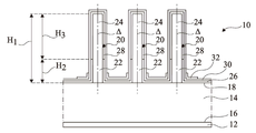
광전자 기기(10)는 도 1의 밑에서 위로:The
제1 바이어싱 전극(biasing electrode)(12)과;A first biasing electrode (12);
예를 들어 반도체의 기판(14)으로, 평행한 표면(16, 18)들을 포함하며, 한 표면(16)은 전극(12)과 접촉하고, 다른 표면(18)은 와이어들을 조직된 형태로 성장시키도록 처리되며, 이 처리는 기판(14)의 표면에 층(layer)(도시 안 됨)의 형성을 포함하는 기판(14)과;For example a
축 Δ와 높이 H1을 가지는 와이어(20)들(세 와이어들이 도시됨)로, 각 와이어는 표면(18)에 접촉하는 높이 H2의 하부(lower portion; 22)와 높이 H3의 상부(upper portion; 24)를 포함하는 와이어(20)들과;Each wire has a
각 하부(22)의 일부의 둘레(periphery)를 덮고(covering) 와이어(20)들 사이의 기판(14)을 덮는 절연층(insulating layer: 26)과;An insulating
각 상부(24)를 덮는 쉘(shell; 28)과;A
쉘(28)과 절연층(26)을 덮는 제2 전극층(30)과; 그리고A second electrode layer (30) covering the shell (28) and the insulating layer (26); And
와이어(2)들 사이의 제2 전극층(30)을 덮으며, 가능하기로 각 와이어(20)의 상부(24)로 연장됨이 없이 각 와이어(20)의 하부(22) 상으로 연장되는 도전부(conductive portion; 32)를Which extends over the
구비한다.Respectively.
각 와이어(20)는 적어도 부분적으로 반도체 재질로 구성된다. 한 실시예에 의하면, 이 반도체 재질은 III-V족 화합물, II-VI족 화합물을 포함하는 그룹, 또는 IV족 반도체 또는 화합물 그룹으로부터 선택된다.Each
각 와이어(20)와 관련 쉘(28)에 의해 형성되는 조립체는 발광다이오드를 구성한다. 쉘(28)은 특히 발광다이오드에 의해 발생되는 전자기 복사의 대부분이 방출되는 층인 활성 영역(active area)을 구비한다. 한 예에 의하면, 활성 영역은 복수의 양자우물(quantum well) 등의 격리 수단(confinement means)을 구비한다. 이 실시예에서, 적어도 어떤 발광다이오드들은 공통 전극들을 가져 전압이 전극(12, 30)들 간에 인가되었을 때 이 발광다이오드들의 활성 영역으로부터 광 복사가 방출된다.The assembly formed by each
광전자 기기(10)의 발광다이오드들은 발광다이오드들의 한 조립체, 두 조립체, 둘보다 많은 조립체들에 분포될 수 있다. 각 조립체는 소수의 발광다이오드로부터 수백만 개의 발광다이오드까지 구비할 수 있다.The light emitting diodes of the
이 실시예에서, 절연층(26)은 각 와이어(20)들에 대한 쉘(28)을 구획(delimit)하고 전극층(30)과 기판(14) 사이에 전기적 절연을 제공한다.In this embodiment, the insulating
이 실시예에서, 도전부(32)는 전극층(30)의 저항을 감소시킬 수 있어 유용하다. 바람직하기로 도전부(32)는 반사성(reflective)이어서, 발광다이오드에 의해 방출되어 광전자 기기(10)로부터 탈출하는 복사의 비율을 증가시킬 수 있어 유용하다.In this embodiment, the
도 2a 내지 2p는 도 1에 도시된 광전자 기기를 제조하는 방법의 다른 실시예의 순차적인 단계들에서 얻어진 구조들의 부분 개략 단면도들이다.Figures 2a-2p are partial schematic cross-sectional views of structures obtained in sequential steps of another embodiment of a method of manufacturing an optoelectronic device shown in Figure 1;
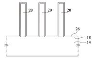
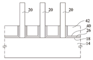
도 2a는 기판(14) 상에 와이어(20)들의 성장의 결과로 얻어진 구조를 도시한다.2A shows a structure obtained as a result of the growth of the
기판(14)은 단일 블록 구조이거나 다른 재질로 구성된 지지부를 덮는 층에 해당할 수 있다. 기판(14)은 바람직하기로, 예를 들어 실리콘, 게르마늄, 탄화규소(Silicone Carbide), GaN 또는 GaAs 등의 III-V족 화합물로 구성된 반도체 기판, 또는 ZnO 기판, 또는 예를 들어 금속 또는 금속 화합물, 특히 구리, 티타늄, 몰리브덴, 그리고 철로 구성된 도전성 기판이다. 바람직하기로 기판(14)은 단결정(single-crystal) 실리콘 기판이다. 바람직하기로, 이는 마이크로일렉트로닉스(microelectronics)에서 구현되는 제조방법에 적합한 반도체 기판이다. 기판(14)은 SOI로도 불리는 절연층 상 실리콘(silicon-on-insulator) 방식의 다층 구조가 될 수도 있다. 이 경우, 전극(12)은 기판(14)의 표면(18) 측 상에 형성될 수 있다. 기판(14)은 중하게 도핑되거나(doped), 경하게 도핑되거나, 도핑되지 않을 수 있다.The
원하는 위치에 와이어(20)들의 성장을 촉진하는 기판(14)의 전처리(previous treatment)가 제공될 수 있다. 와이어 성장을 촉진하도록 기판에 적용되는 처리는 문헌 US 7829443, FR 2995729, 또는 FR 2997558A에 기재된 처리방법들 중의 하나가 될 수 있다.A pretreatment of the
와이어(20)는 적어도 부분적으로, 예를 들어 III-N 화합물 등의 III-V족 화합물을 주로 포함하는 반도체 재질로 구성될 수 있다. III 족 원소의 예들은 갈륨(Ga), 인듐(In), 또는 알루미늄(Al)을 포함한다. III-N 화합물의 예들은 GaN, AlN, InN, InGaN, AlGaN, 또는 AlInGaN을 포함한다. 다른 V족 원소들도 역시 사용될 수 있는데, 예를 들어 인 또는 비소이다. 일반적으로, III-V족 화합물들이 다른 몰분율(molar fraction)들로 조합될 수 있다.The
와이어(20)는 적어도 부분적으로, II-VI족 화합물을 주로 포함하는 반도체 재질에 기반하여 구성된다. II족 원소들의 예는 특히 베릴륨(Be)과 마그네슘(Mg) 등의 IIA족 원소, 특히 아연(Zn), 카드뮴(Cd), 및 수은(Hg) 등의 IIB족 원소들을 포함한다. VI족 원소들의 예는 특히 산소(O)와 텔루륨(Te) 등의 VIA족 원소들을 포함한다. I-VI족 화합물의 예들은 ZnO, ZnMgO, CdZnO, CdZnMgO, CdHgTe, CdTe, 또는 HgTe이다. 일반적으로, II-VI족 화합물 내의 원소들이 다른 몰분율로 조합될 수 있다.The
와이어(20)는 적어도 부분적으로, 적어도 하나의 IV족 화합물을 주로 포함하는 반도체 재질로 구성될 수 있다. IV족 반도체 재질의 예는 실리콘(Si), 탄소(C), 게르마늄(Ge), 탄화규소 합금(SiC), 실리콘-게르마늄 합금(SiGe), 또는 탄화게르마늄 합금(GeC)이다.The
각 와이어(20)의 높이 H1은 250 nm 내지 50 μm, 바람직하기로 1 μm 내지 20 μm의 범위가 될 수 있다. 각 와이어(20)는 표면(18)에 거의 직교하는 축을 따라 연장되는 반도체 구조를 가질 수 있다. 각 와이어(20)는 일반적으로 원통형의 형상을 가질 수 있다. 두 인접 와이어(20)들의 축들은 0.5 μm 내지 20 μm, 바람직하기로 3 μm 내지 20 μm만큼 이격될 수 있다. 일례로서, 와이어(20)들은 규칙적으로, 특히 육각형 또는 정사각형 망(network)으로 분포될 수 있다.The height H1 of each
와이어(20)들의 단면은 예를 들어 타원형, 원형, 또는 특히 삼각형, 사각형, 또는 육각형 등의 다각형 등의 다른 형상들을 가질 수 있다. 그러므로 "직경" 또는 "평균직경"이라는 용어는 와이어 또는 이 와이어 상에 적층된 층의 단면에 있어서, 예를 들어 와이어의 단면적과 동일한 표면적을 가지는 원판(disk)의 직경에 해당되는 등 이 단면 내의 목표 구조의 표면에 관련된 양(quantity)을 지칭하는 것으로 이해되어야 할 것이다. 각 와이어(20)의 평균직경은 50 nm 내지 10 μm, 바람직하기로 200 nm 내지 10 μm의 범위가 될 수 있다. The cross-section of the
와이어 성장 방법은 화학적 기상증착(chemical vapor deposition; CVD) 또는 금속-유기 기상 에피택시(metal-organic vapor phase epitaxy; MOVPE)로도 불리는 금속-유기 화학적 기상증착(metal-organic chemical vapor deposition; MOCVD) 등의 방법이 될 수 있다. 그러나 분자선 에피택시(molecular-beam epitaxy; MBE), 가스원 MBE(gas-source MBE; GSMBE), 금속-유기 MBE(metal-organic MBE; MOMBE), 플라즈마 보조 MBE(plasma-assisted MBE; PAMBE), 원자층 에피택시(atomic layer epitaxy; ALE), 또는 증기액상증착법(hydride vapor phase epitaxy; HVPE) 등의 방법들도 사용될 수 있다. 또한 예를 들어 화학조 증착(chemical bath deposition; CBD), 열수 공정(hydrothermal process)들, 액체 연무 열분해(liquid aerosol pyrolysis), 또는 전착(electrodeposition) 등의 전기화학적 공정(electrochemical process)들 역시 사용될 수 있다.The wire growth method may include metal-organic chemical vapor deposition (MOCVD), also referred to as chemical vapor deposition (CVD) or metal-organic vapor phase epitaxy (MOVPE) . However, molecular-beam epitaxy (MBE), gas-source MBE (GSMBE), metal-organic MBE (MOMBE), plasma-assisted MBE (PAMBE) Methods such as atomic layer epitaxy (ALE) or hydride vapor phase epitaxy (HVPE) may also be used. Electrochemical processes such as, for example, chemical bath deposition (CBD), hydrothermal processes, liquid aerosol pyrolysis, or electrodeposition may also be used have.
일례로서, 방법은 III족 원소의 전구물질(precursor)과 V족 원소의 전구물질을 반응조 내에 분사하는 단계를 포함한다. III족 원소의 전구물질의 예들은 트리메틸갈륨(trimethylgallium; TMGa), 트리에틸갈륨(triethylgallium; TEGa), 트리메틸인듐(trimethylindium; TMIn), 또는 트리메틸알루미늄(trimethylaluminum; TMAl)이다. V족 원소의 전구물질의 예들은 암모니아(NH3), 3부틸포스핀(tertiarybutylphosphine; TBP), 아르신(arsine; AsH3), 또는 디메틸하이드라진(dimethylhydrazine; UDMH)이다.As an example, the method includes injecting a precursor of a Group III element and a precursor of a Group V element into a reaction vessel. Examples of precursors of Group III elements are trimethylgallium (TMGa), triethylgallium (TEGa), trimethylindium (TMIn), or trimethylaluminum (TMAl). Examples of precursors of Group V elements are ammonia (NH 3 ), tertiarybutylphosphine (TBP), arsine (AsH 3 ), or dimethylhydrazine (UDMH).
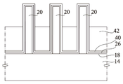
도 2b는 모든 와이어(20) 상과 와이어(20)들 사이의 표면(18) 상에 절연층(26)을 적층한 결과로 얻어진 구조를 도시한다. 절연층(26)은 예를 들어, 산화규소(SiO2), 질화규소(SixNy, 예를 들어 x가 대략 3이고 y가 대략 4일 때 Si3N4), 산화질화규소(silicon oxynitride)(예를 들어 Si2ON2 등 특히 일반식 SiOxNy), 산화하프늄(HfO2), 산화알루미늄(Al2O3), 또는 다이아몬드 등의 유전 재질(dielectric material)로 구성된다. 일례로서, 절연층(16)의 두께는 5 nm 내지 1 μm, 바람직하기로 10 nm 내지 500 nm의 범위로, 예를 들어 약 300 nm이다. 절연층(26)은 예를 들어 플라즈마 강화 화학적 기상증착(plasma-enhanced chemical vapor deposition; PECVD), 저압 화학적 기상증착(low-pressure chemical vapor deposition; LPCVD), 부압 화학적 기상증착(sub-atmospheric chemical vapor deposition; SACVD), CVD, 물리적 기상증착(physical vapor deposition; PVD), 또는 원자층 증착(atomic layer deposition; ALD)에 의해 적층될 수 있다.Figure 2B shows the structure obtained as a result of laminating the insulating
도 2c는 절연층(26) 상에 불투명층(40)을 적층한 결과로 얻어진 구조를 도시한다. 불투명층(40)은 예를 들어 알루미늄(Al), 티타늄(Ti), 구리(Cu), 규소 또는 중석(W)과 알루미늄의 합금 등 금속 또는 금속 합금으로 구성된다. 불투명층(40)의 두께는 50 nm 내지 1 μm, 바람직하기로 100 nm 내지 200 nm의 범위로, 예를 들어 150 nm이다. 불투명층(40)은 예를 들어 PVD, CVD, 또는 ALD에 의해 적층된다.Fig. 2C shows the structure obtained as a result of laminating the
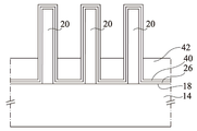
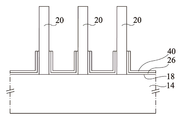
도 2d는 전체 구조 위에 레지스트(resist)의 층을 적층한 다음 얻어진 구조를 도시한다. 레지스트 층(42)은 특히 와이어(20)들 사이에 존재한다. 레지스트 층(42)의 최대 두께는 와이어(20)의 높이 H1보다 더 크다. 레지스트 층(42)의 최대 두께는 250 nm 내지 50 μm의 범위이다. Figure 2D shows the structure obtained after laminating a layer of resist over the entire structure. The resist
도 2e는 레지스트 층(42)의 상부만이 제거되는 레지스트 층(42)의 부분적 식각(etching)의 제1 단계의 결과로 얻어진 구조를 도시한다. 제1 식각 단계 이후 레지스트 층(42)에서 제거되는 두께는 수 마이크로미터이다. 제1 식각 단계는 바람직하기로, 예를 들어 레지스트 층(42)을 자외선 복사에 노출시킴으로써 레지스트 층(42)을 노광(illuminating)시키는 단계와, 그리고 예를 들어 레지스트를 현상액(developer)과 접촉하도록 위치시키는 액상 식각(liquid etching)에 의해 레지스트 층의 일부를 제거하는 레지스트 층의 현상(developing) 단계를 포함하는 사진식각(photolithography) 단계이다. 레지스트는 양의(positive) 레지스트, 즉 적용된 복사에 노출된 부분이 현상액에 용해성이고 노출되지 않은 부분이 비용해성으로 남게 될 수 있다. 그러면 특히 노광 에너지 및/또는 노광 시간의 조정에 의한 수지(resin)의 부분적 노광 및 현상이 구현될 수 있다. 복사 에너지는 예를 들어 20 내지 100 mW/cm2의 범위가 될 수 있다. 노광 시간은 예를 들어 수 초 내지 수백 초의 범위가 될 수 있다. 레지스트는 음의(negative) 레지스트, 즉 적용된 복사에 노출된 부분이 현상액에 비용해성이고 노출되지 않은 부분이 용해성으로 남게 될 수 있다. 이 경우, 레지스트의 노광이 없거나 현상에 이은 노광과 함께 노광 시간의 조정에 의한 레지스트의 부분적 현상이 구현될 수 있다.Figure 2E shows the resulting structure resulting from the first step of partial etching of the resist
한 실시예에 의하면, 와이어(20)들은 적어도 부분적으로 투명할 수 있다. 그러면 불투명층(40)의 존재는, 레지스트 층(42)의 와이어(20) 주변 부분의 원치 않는 과다노출을 야기할 수 있는 와이어(20)들에 의한 노광 복사의 유도를 감소시키거나 심지어 억제할 수 있다.According to one embodiment, the
도 2f는 이전 단계의 결과로 얻어진 레지스트 층(42)의 상부만이 제거되는 레지스트 층(42)을 다시 부분적 식각하는 레지스트 층(42)의 식각의 제2 단계의 결과로 얻어진 구조를 도시한다. 제2 식각 단계 이후 레지스트 층(42)에서 제거되는 두께는 수백 나노미터 내지 수 마이크로미터의 범위이다. 제2 식각 단계는 바람직하기로 산소 기반 플라즈마를 사용하는 식각 단계이다.2F shows a structure obtained as a result of the second step of etching the resist
한 실시예에 의하면, RIE(reactive ion etching; 반응성 이온 식각)과 고밀도 플라즈마 소스(source) 등의 임의의 종래의 식각 소스, 특히 유기 재질의 식각에 사용되는 임의의 종류의 식각 소스가 본 발명에 의한 플라즈마 식각 방법에 사용될 수 있다. 여기 전력(excitation power)은 10 W 내지 1 kW의 범위가 될 수 있다. 기판은 예를 들어 20℃의 실온(room temperature)에 유지될 수 있다.According to one embodiment, any conventional etch source, such as reactive ion etching (RIE) and high density plasma source, in particular any kind of etch source used in etching organic materials, Gt; etch. ≪ / RTI > The excitation power may range from 10 W to 1 kW. The substrate may be maintained at room temperature, for example, at 20 占 폚.
플라즈마 식각의 사용은 레지스트 층(42)의 바람직한 높이에 정확하고 반복적으로 도달할 수 있게 하여 유용하다. 또한 플라즈마의 사용은 특히 원치 않는 유기 잔류물을 제거함으로써 노출된 표면을 후속 단계들을 위해 청소한다. 이는 또한 사진식각의 노출 동안 기존의 와이어들과 층들의 형성에 기인하여 특히 레지스트 띠의 협소화(노칭; notching)를 야기하는 기생 효과(parasitic effect)들을 방지할 수 있다.The use of plasma etch is useful by allowing accurate and repeatable reaching of the desired height of the resist
도 2g는 레지스트 층(42)에 덮이지 않은 불투명층(40)의 부분을 식각하는 단계와 더 이상 불투명층(40)으로 덮이지 못하는 절연층(26)의 부분을 식각하는 단계의 결과로 얻어진 구조를 도시한다. 불투명층(40)의 식각은 습식 또는 건식 식각(플라즈마 식각)이 될 수 있다. 절연층(26)의 식각은 습식 또는 건식 식각(플라즈마 식각)이 될 수 있다. 바람직하기로 식각들은 레지스트에 대해 선택적이다.2G shows the result of etching the portion of the
도 2h는 남은 레지스트 층을 제거하는 단계의 결과로 얻어진 구조를 도시한다. 남은 레지스트 층의 제거는 도 2g의 구조를 레지스트 층(42)을 용해할 수 있는 용제가 담긴 처리조(bath)에 침지(dipping)함으로써 수행될 수 있다.Figure 2h shows the structure obtained as a result of removing the remaining resist layer. Removal of the remaining resist layer can be performed by dipping the structure of Fig. 2G into a treatment bath containing a solvent capable of dissolving the resist
도 2i는 불투명층(40)의 식각 단계의 결과로 얻어진 구조를 도시한다. 식각은 와이어(20)들 상과 절연층(26) 상에 선택적인 습식 또는 건식 식각(플라즈마 식각)이 될 수 있다.2I shows the structure obtained as a result of the etching step of the
이하 설명될 단계 2J 내지 2P는 도 1에 도시된 구조를 형성할 수 있다. 일반적으로, 방법의 후속 단계들은 예상되는 응용분야에 따라 달라진다.Steps 2J to 2P to be described below can form the structure shown in Fig. In general, the subsequent steps of the method will depend on the expected application area.
도 2j는:2J shows:
예를 들어 MOCVD에 의해 각 와이어(20)에 쉘(28)을 형성하는 단계와;Forming a shell (28) on each wire (20) by, for example, MOCVD;
예를 들어 MOCVD, ALD, PVD, CVD, 또는 PECVD에 의해 제1 전극(30)을 형성하는 단계와; 그리고Forming the
예를 들어 PVD, ALD, CVD, 또는 진공증착(vacuum evaporation)에 의해 제1 전극(30)을 덮는 도전층(conductive layer; 44)을 형성하는 단계Forming a
의 단계들을 거쳐 얻어진 구조를 도시한다. ≪ / RTI > FIG.
전극(30)은 각 와이어(20)를 덮는 쉘(28)의 활성 영역에 전역을 공급(biasing)하여 발광다이오드에 의해 전자기 복사를 방출하도록 할 수 있다. 전극(30)을 구성하는 재질은 알루미늄 또는 갈륨 또는 붕소, 또는 그래핀(graphene)으로 도핑되거나 도핑되지 않은 산화인듐주석(indium tin oxide; ITO), 산화아연 등의 투명하고 도전성인 재질이 될 수 있다. 일례로서, 전극층(30)은 20 nm 내지 500 nm, 바람직하기로 100 nm 내지 200 nm 범위의 두께를 가진다.The
도전층(44)은 예를 들어 알루미늄, 은, 구리, 금, 또는 루테늄이나 적어도 두 이들 화합물의 합금 등의 금속층이 될 수 있다. 일례로서, 도전층(44)은 100 내지 2,000 nm의 두께를 가진다. 바람직하기로 도전층(44)은 반사성(reflective)이다.The
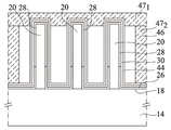
도 2k는 전체 구조 상에 레지스트의 층(46)이 적층된 결과로 얻어진 구조를 도시한다. 레지스트 층(46)은 특히 와이어(20)들 사이에 존재한다. 레지스트 층(46)의 최대 두께는 바람직하기로 쉘(28)과 전극(30)과 도전층(44)으로 덮인 와이어(20)들의 높이보다 더 크다. 레지스트 층(46)의 최대 두께는 250 nm 내지 50 μm의 범위이다. 레지스트 층(46)은 레지스트 층(42)과 동일한 조성을 가질 수 있다.Figure 2K shows the structure obtained as a result of the layer of resist 46 being deposited on the overall structure. The resist
도 2l은 레지스트 층(46)의 상부만이 노출되는 제1 부분적 노광과 특히 마스킹 스크린(masking screen)의 사용에 의한 제2 부분적 노광의 결과로 얻어진 구조를 도시한다. 두 노광 단계들은 결과적으로 와이어(20)들의 높이까지의 부분만으로 와이어(20)들 사이의 도전층(44) 상에 연장되는 레지스트 블록(48)을 제외하고 전체 레지스트 층(46)을 노광시키게 된다. 도 2L에서, 빗금 영역(471)은 제1 노광 단계 동안 노출되는 레지스트 층(46)의 상부를 지시하며, 빗금 영역(472)은 제2 노광 단계 동안 노출되는 레지스트 층(460의 추가 영역을 지시한다.FIG. 21 shows the structure obtained as a result of the first partial exposure, in which only the upper part of the resist
도 2m은 레지스트 블록(48)을 얻게 된 식각 단계의 결과로 얻어진 구조를 도시한다. 식각은 바람직하기로 사직식각의 레지스트 층(46)을 현상(developing)하는 단계이다. 2M shows the structure obtained as a result of the etching step in which the resist
도 2n은 레지스트 블록(48)의 상부만이 제거되는 레지스트 블록(48)의 제2 식각 단계의 결과로 얻어진 구조를 도시한다. 이 단계는 도 2f에서 레지스트 층(42)의 제2 식각 단계에 관련하여 전술한 바와 같이 플라즈마 식각으로 수행될 수 있다.2N shows the structure obtained as a result of the second etching step of the resist
도 2o는 도전층(44)의 레지스트 블록(48)로 덮이지 않은 부분을 식각하는 단계의 결과로 얻어진 구조를 도시한다. 도전부(32)는 이와 같이 형성된다. 도전층(44)의 식각은 습식 또는 건식 식각(플라즈마 식각)일 수 있다. 바람직하기로 이 식각은 레지스트와 전극층(30)에 대해 선택적이다.2O shows the structure obtained as a result of the step of etching the portion of the
도 2p는 레지스트 블록(48)의 제거 단계로 얻어진 구조를 도시한다. 2P shows the structure obtained by the removal step of the resist
Claims (10)
a) 마이크로와이어 또는 나노와이어들을 절연층(26)으로 덮는 단계와;
b) 절연층을 불투명층(40)으로 덮는 단계와;
c) 와이어들 사이의 기판 상에 연장되는 제1 레지스트 층(42)을 적층시키는 단계와;
d) 제1 레지스트 층을 사진식각에 의해 제1 두께만큼 식각하는 단계와;
e) 단계 d)의 결과 남은 제1 레지스트 층을 플라즈마 식각에 의해 제2 두께만큼 식각하는 단계와;
f) 단계 e)의 결과 남은 제1 레지스트 층에 덮이지 않은 불투명층의 부분을 식각하는 단계와;
g) 불투명층으로 덮이지 않은 절연층의 부분을 식각하는 단계와;
h) 단계 e)의 결과 남은 제1 레지스트 층을 제거하는 단계와; 그리고
i) 불투명층을 제거하는 단계
들의 순차적인 단계들을 구비하는 전자기기의 제조방법.A method of manufacturing an electrooptical device (10) comprising a substrate (14) and microwires or nanowires (20) supported on the substrate, the method comprising:
a) covering the microwires or nanowires with an insulating layer (26);
b) covering the insulating layer with an opaque layer (40);
c) laminating a first resist layer (42) extending over the substrate between the wires;
d) etching the first resist layer by photolithography to a first thickness;
e) etching the remaining first resist layer as a result of step d) by a second thickness by plasma etching;
f) etching a portion of the opaque layer not covered by the first resist layer remaining as a result of step e);
g) etching a portion of the insulating layer not covered by the opaque layer;
h) removing the remaining first resist layer as a result of step e); And
i) removing the opaque layer
Wherein the steps of:
마이크로와이어 또는 나노와이어(20)들의 높이가 250 nm 내지 50 μm의 범위에 있는
전자기기의 제조방법.In claim 1,
When the height of the microwires or nanowires 20 is in the range of 250 nm to 50 mu m
A method of manufacturing an electronic device.
단계 c)에서의 제1 레지스트 층(42)의 최대 두께가 마이크로와이어 또는 나노와이어(20)들의 높이보다 더 큰
전자기기의 제조방법.[Claim 2]
If the maximum thickness of the first resist layer 42 in step c) is greater than the height of the microwires or nanowires 20
A method of manufacturing an electronic device.
절연층(26)의 두께가 5 nm 내지 1 μm의 범위에 있는
전자기기의 제조방법.4. The method according to any one of claims 1 to 3,
When the thickness of the insulating layer 26 is in the range of 5 nm to 1 mu m
A method of manufacturing an electronic device.
플라즈마 식각이 산소 플라즈마 식각인
전자기기의 제조방법.5. The method according to any one of claims 1 to 4,
Plasma etching is an oxygen plasma etching
A method of manufacturing an electronic device.
불투명층(40)이 금속 또는 금속 합금으로 구성되는
전자기기의 제조방법.6. The method according to any one of claims 1 to 5,
When the opaque layer 40 is made of a metal or a metal alloy
A method of manufacturing an electronic device.
불투명층(40)의 두께가 5 nm 내지 1 μm의 범위에 있는
전자기기의 제조방법.7. The method according to any one of claims 1 to 6,
When the thickness of the opaque layer 40 is in the range of 5 nm to 1 mu m
A method of manufacturing an electronic device.
j) 각 마이크로와이어 또는 나노와이어(20)들의 절연층(26)으로 덮이지 않은 부분 상에 쉘(28)을 형성하는 단계로, 쉘이 전자기기에서 공급되거나 포착되는 복사의 대부분을 포착하거나 방출할 수 있는 활성 영역을 구비하는 단계와;
k) 쉘 상과 절연층 상에 전극층(30)을 형성하는 단계와;
l) 전극층을 도전층(44)으로 덮는 단계와;
m) 와이어들 사이의 도전층 상에 연장되는 제2 레지스트 층(46)을 적층시키는 단계와;
n) 제2 레지스트 층을 사진식각에 의해 구획하여 마이크로와이어 또는 나노와이어(20)들 상에 연장되는 레지스트 블록(48)을 형성하는 단계와;
o) 레지스트 블록을 플라즈마 식각에 의해 제3 두께만큼 식각하는 단계와;
p) 단계 o)의 결과로 남은 레지스트 블록으로 덮이지 않은 제2 반사성 도전층의 일부를 식각하는 단계와; 그리고
q) 단계 o)의 결과로 남은 제2 레지스트 층을 제거하는 단계
의 순차적인 단계들을 더 구비하는 전자기기의 제조방법.The method according to any one of claims 1 to 7, wherein after step i):
j) forming a shell (28) on a portion of each microwire or nanowire (20) not covered by an insulating layer (26), wherein the shell captures or emits most of the radiation supplied or captured in the electronics Said method comprising the steps of:
k) forming an electrode layer (30) on the shell and the insulating layer;
l) covering the electrode layer with a conductive layer (44);
m) stacking a second resist layer (46) extending over the conductive layer between the wires;
n) separating the second resist layer by photolithography to form a resist block 48 extending over the microwires or nanowires 20;
o) etching the resist block by a plasma etch to a third thickness;
p) etching a portion of the second reflective conductive layer not covered by the remaining resist block as a result of step o); And
q) removing the remaining second resist layer as a result of step o)
The method comprising the steps of:
r) 제2 레지스트 층(46)을 제4 두께만큼 부분적으로 노광시키는 단계와;
s) 마스킹 스크린을 사용하여 제2 레지스트 층의 부분을 전체 두께만큼 노광시키는 단계와; 그리고
t) 단계 r)과 s)에서 노광된 제2 레지스트 층의 부분들을 식각하는 단계
들을 포함하는 전자기기의 제조방법.8. The method of claim 8, wherein step n) comprises:
r) partially exposing the second resist layer 46 to a fourth thickness;
s) exposing a portion of the second resist layer to a full thickness using a masking screen; And
t) etching the portions of the second resist layer exposed in steps r) and s)
The method comprising the steps of:
도전층(44)이 반사성인
전자기기의 제조방법.In claim 8 or 9,
When the conductive layer 44 is reflective
A method of manufacturing an electronic device.
Applications Claiming Priority (3)
| Application Number | Priority Date | Filing Date | Title |
|---|---|---|---|
| FR1463372 | 2014-12-29 | ||
| FR1463372A FR3031242B1 (en) | 2014-12-29 | 2014-12-29 | METHOD FOR MANUFACTURING ISOLATED FOOT SEMICONDUCTOR NANOWIRS OR MICROFILES |
| PCT/FR2015/053758 WO2016108023A1 (en) | 2014-12-29 | 2015-12-24 | Process for fabricating semiconductor nanowires or microwires having insulated roots |
Publications (2)
| Publication Number | Publication Date |
|---|---|
| KR20170101242A true KR20170101242A (en) | 2017-09-05 |
| KR102414850B1 KR102414850B1 (en) | 2022-06-29 |
Family
ID=52779830
Family Applications (1)
| Application Number | Title | Priority Date | Filing Date |
|---|---|---|---|
| KR1020177019191A KR102414850B1 (en) | 2014-12-29 | 2015-12-24 | Process for fabricating semiconductor nanowires or microwires having insulated roots |
Country Status (5)
| Country | Link |
|---|---|
| US (1) | US9954141B2 (en) |
| EP (1) | EP3241246B1 (en) |
| KR (1) | KR102414850B1 (en) |
| FR (1) | FR3031242B1 (en) |
| WO (1) | WO2016108023A1 (en) |
Families Citing this family (5)
| Publication number | Priority date | Publication date | Assignee | Title |
|---|---|---|---|---|
| DE102015104144A1 (en) * | 2015-03-19 | 2016-09-22 | Osram Opto Semiconductors Gmbh | Optoelectronic semiconductor body and method for producing an optoelectronic semiconductor body |
| FR3068514B1 (en) | 2017-06-30 | 2019-08-09 | Aledia | OPTOELECTRONIC DEVICE |
| FR3076078B1 (en) | 2017-12-27 | 2021-11-26 | Aledia | OPTOELECTRONIC DEVICE WITH THREE-DIMENSIONAL DIODE MATRIX |
| FR3093861B1 (en) * | 2019-03-12 | 2021-09-17 | Commissariat Energie Atomique | Chip coating process |
| FR3137498A1 (en) | 2022-06-30 | 2024-01-05 | Aledia | Optoelectronic device and method of manufacturing such a device |
Citations (3)
| Publication number | Priority date | Publication date | Assignee | Title |
|---|---|---|---|---|
| KR100846514B1 (en) * | 2007-02-05 | 2008-07-17 | 삼성전자주식회사 | Method of selective-etching thin film formed on vertical structure and method of manufacturing memory device using the same method |
| WO2014064395A1 (en) * | 2012-10-26 | 2014-05-01 | Aledia | Optoelectronic device and method for manufacturing same |
| WO2014196920A1 (en) * | 2013-06-05 | 2014-12-11 | Sol Voltaics Ab | A solar cell structure and a method of its fabrication |
Family Cites Families (7)
| Publication number | Priority date | Publication date | Assignee | Title |
|---|---|---|---|---|
| FR1463372A (en) | 1965-01-11 | 1966-12-23 | Internal combustion engine with rotary piston | |
| AU2008203934C1 (en) | 2007-01-12 | 2014-03-13 | Qunano Ab | Nitride nanowires and method of producing such |
| WO2010062644A2 (en) | 2008-10-28 | 2010-06-03 | The Regents Of The University Of California | Vertical group iii-v nanowires on si, heterostructures, flexible arrays and fabrication |
| FR2995729B1 (en) | 2012-09-18 | 2016-01-01 | Aledia | SEMICONDUCTOR MICROFILL OR NANOWILE OPTOELECTRIC DEVICE AND METHOD FOR MANUFACTURING THE SAME |
| US9537044B2 (en) * | 2012-10-26 | 2017-01-03 | Aledia | Optoelectric device and method for manufacturing the same |
| US9500519B2 (en) * | 2012-12-03 | 2016-11-22 | Yale University | Superconducting single photon detector |
| US9773669B2 (en) * | 2014-09-11 | 2017-09-26 | Ramot At Tel-Aviv University Ltd. | Method of fabricating a nanoribbon and applications thereof |
-
2014
- 2014-12-29 FR FR1463372A patent/FR3031242B1/en not_active Expired - Fee Related
-
2015
- 2015-12-24 EP EP15823722.2A patent/EP3241246B1/en active Active
- 2015-12-24 US US15/538,148 patent/US9954141B2/en active Active
- 2015-12-24 WO PCT/FR2015/053758 patent/WO2016108023A1/en active Application Filing
- 2015-12-24 KR KR1020177019191A patent/KR102414850B1/en active IP Right Grant
Patent Citations (3)
| Publication number | Priority date | Publication date | Assignee | Title |
|---|---|---|---|---|
| KR100846514B1 (en) * | 2007-02-05 | 2008-07-17 | 삼성전자주식회사 | Method of selective-etching thin film formed on vertical structure and method of manufacturing memory device using the same method |
| WO2014064395A1 (en) * | 2012-10-26 | 2014-05-01 | Aledia | Optoelectronic device and method for manufacturing same |
| WO2014196920A1 (en) * | 2013-06-05 | 2014-12-11 | Sol Voltaics Ab | A solar cell structure and a method of its fabrication |
Also Published As
| Publication number | Publication date |
|---|---|
| KR102414850B1 (en) | 2022-06-29 |
| FR3031242B1 (en) | 2016-12-30 |
| EP3241246B1 (en) | 2018-10-31 |
| FR3031242A1 (en) | 2016-07-01 |
| US20180019376A1 (en) | 2018-01-18 |
| WO2016108023A1 (en) | 2016-07-07 |
| US9954141B2 (en) | 2018-04-24 |
| EP3241246A1 (en) | 2017-11-08 |
Similar Documents
| Publication | Publication Date | Title |
|---|---|---|
| KR102060392B1 (en) | Nanopyramid sized opto-electronic structure and method for manufacturing of same | |
| KR102414850B1 (en) | Process for fabricating semiconductor nanowires or microwires having insulated roots | |
| US20110127554A1 (en) | Light emitting device and method of manufacturing the same | |
| EP2359416A1 (en) | A nanostructured device | |
| US20140014897A1 (en) | Semiconductor light emitting device with doped buffer layer and method of manufacturing the same | |
| KR20100073757A (en) | Light emitting device using micro-rod and method of manufacturing the light emitting device | |
| US10153399B2 (en) | Optoelectronic device comprising semiconductor elements and its fabrication process | |
| KR20220024162A (en) | Axial optoelectronic device having light emitting diode and manufacturing method therefor | |
| KR102633272B1 (en) | Optoelectronic device including light-emitting components and transistors | |
| US10026870B2 (en) | Optoelectronic device having semiconductor elements | |
| CN107078186B (en) | Optoelectronic device with 3 D semiconductor element | |
| KR101373398B1 (en) | Method for preparing high efficiency Light Emitting Diode thereof | |
| US20170365737A1 (en) | Optoelectronic device comprising three-dimensional semiconductor elements and method for the production thereof | |
| TWI437731B (en) | Semiconductor optoelectronic device with enhanced light extraction efficiency and fabricating method thereof | |
| KR101383161B1 (en) | Light emitting diode and method of manufacturing the diode | |
| US20190181329A1 (en) | Method to achieve active p-type layer/layers in iii-nitride epitaxial or device structures having buried p-type layers | |
| EP3712963B1 (en) | Method of making a photoelectrode for solar water splitting | |
| CN106030831A (en) | Method for producing semiconductor layer sequence and optoelectronic semiconductor component | |
| KR100818459B1 (en) | Light emitting devices and manufacturing method of the same | |
| KR20160003378A (en) | Light emitting structure and Light emitting device having the same | |
| KR20140036396A (en) | Light emitting diode comprising porous transparent electrode and method of fabricating the same | |
| KR101171328B1 (en) | High efficiency light emitting diode | |
| Jakhar et al. | A top-down approach for fabrication of nanorods on GaN-based LEDs using self-assembled Ni | |
| KR101403715B1 (en) | Light emitting device and method thereof | |
| CN109509815A (en) | A kind of epitaxial wafer of light emitting diode and preparation method thereof |
Legal Events
| Date | Code | Title | Description |
|---|---|---|---|
| A201 | Request for examination | ||
| E902 | Notification of reason for refusal | ||
| E701 | Decision to grant or registration of patent right | ||
| GRNT | Written decision to grant |