KR20170066446A - Electrically conductive patterns with wide line-width and methods for producing same - Google Patents
Electrically conductive patterns with wide line-width and methods for producing same Download PDFInfo
- Publication number
- KR20170066446A KR20170066446A KR1020177010632A KR20177010632A KR20170066446A KR 20170066446 A KR20170066446 A KR 20170066446A KR 1020177010632 A KR1020177010632 A KR 1020177010632A KR 20177010632 A KR20177010632 A KR 20177010632A KR 20170066446 A KR20170066446 A KR 20170066446A
- Authority
- KR
- South Korea
- Prior art keywords
- pattern
- ink
- stamping
- screen
- micrometers
- Prior art date
Links
- 238000000034 method Methods 0.000 title claims abstract description 70
- 239000000758 substrate Substances 0.000 claims abstract description 79
- 239000000463 material Substances 0.000 claims abstract description 63
- 239000000203 mixture Substances 0.000 claims abstract description 18
- 238000007650 screen-printing Methods 0.000 claims abstract description 14
- 239000004205 dimethyl polysiloxane Substances 0.000 claims description 27
- 229920000435 poly(dimethylsiloxane) Polymers 0.000 claims description 27
- 125000000524 functional group Chemical group 0.000 claims description 18
- 229910052751 metal Inorganic materials 0.000 claims description 18
- 239000002184 metal Substances 0.000 claims description 18
- -1 polydimethylsiloxane Polymers 0.000 claims description 18
- 239000011521 glass Substances 0.000 claims description 17
- 239000000839 emulsion Substances 0.000 claims description 16
- 229920006254 polymer film Polymers 0.000 claims description 10
- BQCADISMDOOEFD-UHFFFAOYSA-N Silver Chemical compound [Ag] BQCADISMDOOEFD-UHFFFAOYSA-N 0.000 claims description 8
- 229920001707 polybutylene terephthalate Polymers 0.000 claims description 7
- 229920000139 polyethylene terephthalate Polymers 0.000 claims description 7
- 239000005020 polyethylene terephthalate Substances 0.000 claims description 7
- 229910052709 silver Inorganic materials 0.000 claims description 7
- 239000004332 silver Substances 0.000 claims description 7
- RYGMFSIKBFXOCR-UHFFFAOYSA-N Copper Chemical compound [Cu] RYGMFSIKBFXOCR-UHFFFAOYSA-N 0.000 claims description 5
- 229910052802 copper Inorganic materials 0.000 claims description 5
- 239000010949 copper Substances 0.000 claims description 5
- PCHJSUWPFVWCPO-UHFFFAOYSA-N gold Chemical compound [Au] PCHJSUWPFVWCPO-UHFFFAOYSA-N 0.000 claims description 5
- 229910052737 gold Inorganic materials 0.000 claims description 5
- 239000010931 gold Substances 0.000 claims description 5
- 238000001035 drying Methods 0.000 claims description 4
- 238000005530 etching Methods 0.000 claims description 4
- 238000012360 testing method Methods 0.000 claims description 4
- 238000012546 transfer Methods 0.000 claims description 4
- NIXOWILDQLNWCW-UHFFFAOYSA-M Acrylate Chemical compound [O-]C(=O)C=C NIXOWILDQLNWCW-UHFFFAOYSA-M 0.000 claims description 3
- WQZGKKKJIJFFOK-GASJEMHNSA-N Glucose Natural products OC[C@H]1OC(O)[C@H](O)[C@@H](O)[C@@H]1O WQZGKKKJIJFFOK-GASJEMHNSA-N 0.000 claims description 3
- 239000004372 Polyvinyl alcohol Substances 0.000 claims description 3
- UHPJWJRERDJHOJ-UHFFFAOYSA-N ethene;naphthalene-1-carboxylic acid Chemical compound C=C.C1=CC=C2C(C(=O)O)=CC=CC2=C1 UHPJWJRERDJHOJ-UHFFFAOYSA-N 0.000 claims description 3
- 239000012530 fluid Substances 0.000 claims description 3
- 239000008103 glucose Substances 0.000 claims description 3
- 238000007373 indentation Methods 0.000 claims description 3
- 239000000178 monomer Substances 0.000 claims description 3
- 229920002689 polyvinyl acetate Polymers 0.000 claims description 3
- 239000011118 polyvinyl acetate Substances 0.000 claims description 3
- 229920002451 polyvinyl alcohol Polymers 0.000 claims description 3
- 229910052782 aluminium Inorganic materials 0.000 claims description 2
- XAGFODPZIPBFFR-UHFFFAOYSA-N aluminium Chemical compound [Al] XAGFODPZIPBFFR-UHFFFAOYSA-N 0.000 claims description 2
- 239000000976 ink Substances 0.000 description 123
- 239000010410 layer Substances 0.000 description 30
- 239000013545 self-assembled monolayer Substances 0.000 description 28
- 239000002094 self assembled monolayer Substances 0.000 description 19
- 150000001356 alkyl thiols Chemical class 0.000 description 13
- 150000002898 organic sulfur compounds Chemical class 0.000 description 13
- 239000002904 solvent Substances 0.000 description 10
- 238000010586 diagram Methods 0.000 description 7
- 229920002120 photoresistant polymer Polymers 0.000 description 7
- 238000000682 scanning probe acoustic microscopy Methods 0.000 description 7
- 239000000126 substance Substances 0.000 description 7
- KDLHZDBZIXYQEI-UHFFFAOYSA-N Palladium Chemical compound [Pd] KDLHZDBZIXYQEI-UHFFFAOYSA-N 0.000 description 6
- 238000000813 microcontact printing Methods 0.000 description 6
- BASFCYQUMIYNBI-UHFFFAOYSA-N platinum Chemical compound [Pt] BASFCYQUMIYNBI-UHFFFAOYSA-N 0.000 description 6
- 150000003573 thiols Chemical group 0.000 description 6
- CSCPPACGZOOCGX-UHFFFAOYSA-N Acetone Chemical compound CC(C)=O CSCPPACGZOOCGX-UHFFFAOYSA-N 0.000 description 5
- 229920002799 BoPET Polymers 0.000 description 5
- 238000013459 approach Methods 0.000 description 5
- 125000004432 carbon atom Chemical group C* 0.000 description 5
- XEEYBQQBJWHFJM-UHFFFAOYSA-N Iron Chemical compound [Fe] XEEYBQQBJWHFJM-UHFFFAOYSA-N 0.000 description 4
- XUIMIQQOPSSXEZ-UHFFFAOYSA-N Silicon Chemical compound [Si] XUIMIQQOPSSXEZ-UHFFFAOYSA-N 0.000 description 4
- 150000001504 aryl thiols Chemical class 0.000 description 4
- 230000015572 biosynthetic process Effects 0.000 description 4
- 239000000919 ceramic Substances 0.000 description 4
- 239000011248 coating agent Substances 0.000 description 4
- 238000000576 coating method Methods 0.000 description 4
- 150000001875 compounds Chemical class 0.000 description 4
- 238000012986 modification Methods 0.000 description 4
- 230000004048 modification Effects 0.000 description 4
- 238000007639 printing Methods 0.000 description 4
- 229910052710 silicon Inorganic materials 0.000 description 4
- 239000010703 silicon Substances 0.000 description 4
- ZWEHNKRNPOVVGH-UHFFFAOYSA-N 2-Butanone Chemical compound CCC(C)=O ZWEHNKRNPOVVGH-UHFFFAOYSA-N 0.000 description 3
- XEKOWRVHYACXOJ-UHFFFAOYSA-N Ethyl acetate Chemical compound CCOC(C)=O XEKOWRVHYACXOJ-UHFFFAOYSA-N 0.000 description 3
- VYPSYNLAJGMNEJ-UHFFFAOYSA-N Silicium dioxide Chemical compound O=[Si]=O VYPSYNLAJGMNEJ-UHFFFAOYSA-N 0.000 description 3
- 125000000217 alkyl group Chemical group 0.000 description 3
- 239000011247 coating layer Substances 0.000 description 3
- 238000002508 contact lithography Methods 0.000 description 3
- 238000004519 manufacturing process Methods 0.000 description 3
- 150000002739 metals Chemical class 0.000 description 3
- 229910052763 palladium Inorganic materials 0.000 description 3
- 229910052697 platinum Inorganic materials 0.000 description 3
- 229920000642 polymer Polymers 0.000 description 3
- 125000006850 spacer group Chemical group 0.000 description 3
- 230000008961 swelling Effects 0.000 description 3
- PXHVJJICTQNCMI-UHFFFAOYSA-N Nickel Chemical compound [Ni] PXHVJJICTQNCMI-UHFFFAOYSA-N 0.000 description 2
- 239000002253 acid Substances 0.000 description 2
- 229910045601 alloy Inorganic materials 0.000 description 2
- 239000000956 alloy Substances 0.000 description 2
- 125000003118 aryl group Chemical group 0.000 description 2
- 239000002131 composite material Substances 0.000 description 2
- ZUOUZKKEUPVFJK-UHFFFAOYSA-N diphenyl Chemical compound C1=CC=CC=C1C1=CC=CC=C1 ZUOUZKKEUPVFJK-UHFFFAOYSA-N 0.000 description 2
- 150000002019 disulfides Chemical group 0.000 description 2
- 239000013536 elastomeric material Substances 0.000 description 2
- 238000009472 formulation Methods 0.000 description 2
- 239000012535 impurity Substances 0.000 description 2
- 229910052742 iron Inorganic materials 0.000 description 2
- 239000011133 lead Substances 0.000 description 2
- 229910044991 metal oxide Inorganic materials 0.000 description 2
- 150000004706 metal oxides Chemical class 0.000 description 2
- 238000012552 review Methods 0.000 description 2
- 239000010935 stainless steel Substances 0.000 description 2
- 229910001220 stainless steel Inorganic materials 0.000 description 2
- 125000001424 substituent group Chemical group 0.000 description 2
- 150000003568 thioethers Chemical group 0.000 description 2
- 125000003396 thiol group Chemical group [H]S* 0.000 description 2
- NEAQRZUHTPSBBM-UHFFFAOYSA-N 2-hydroxy-3,3-dimethyl-7-nitro-4h-isoquinolin-1-one Chemical compound C1=C([N+]([O-])=O)C=C2C(=O)N(O)C(C)(C)CC2=C1 NEAQRZUHTPSBBM-UHFFFAOYSA-N 0.000 description 1
- UECUPGFJVNJNQA-UHFFFAOYSA-N 2-phenylbenzenethiol Chemical compound SC1=CC=CC=C1C1=CC=CC=C1 UECUPGFJVNJNQA-UHFFFAOYSA-N 0.000 description 1
- JBRZTFJDHDCESZ-UHFFFAOYSA-N AsGa Chemical compound [As]#[Ga] JBRZTFJDHDCESZ-UHFFFAOYSA-N 0.000 description 1
- 229920002284 Cellulose triacetate Polymers 0.000 description 1
- 239000005046 Chlorosilane Substances 0.000 description 1
- VYZAMTAEIAYCRO-UHFFFAOYSA-N Chromium Chemical compound [Cr] VYZAMTAEIAYCRO-UHFFFAOYSA-N 0.000 description 1
- 229920000742 Cotton Polymers 0.000 description 1
- BWGNESOTFCXPMA-UHFFFAOYSA-N Dihydrogen disulfide Chemical compound SS BWGNESOTFCXPMA-UHFFFAOYSA-N 0.000 description 1
- RWSOTUBLDIXVET-UHFFFAOYSA-N Dihydrogen sulfide Chemical class S RWSOTUBLDIXVET-UHFFFAOYSA-N 0.000 description 1
- 229920002943 EPDM rubber Polymers 0.000 description 1
- 239000004593 Epoxy Substances 0.000 description 1
- 206010073306 Exposure to radiation Diseases 0.000 description 1
- GYHNNYVSQQEPJS-UHFFFAOYSA-N Gallium Chemical compound [Ga] GYHNNYVSQQEPJS-UHFFFAOYSA-N 0.000 description 1
- 229910001218 Gallium arsenide Inorganic materials 0.000 description 1
- BLRPTPMANUNPDV-UHFFFAOYSA-N Silane Chemical compound [SiH4] BLRPTPMANUNPDV-UHFFFAOYSA-N 0.000 description 1
- NINIDFKCEFEMDL-UHFFFAOYSA-N Sulfur Chemical compound [S] NINIDFKCEFEMDL-UHFFFAOYSA-N 0.000 description 1
- ATJFFYVFTNAWJD-UHFFFAOYSA-N Tin Chemical compound [Sn] ATJFFYVFTNAWJD-UHFFFAOYSA-N 0.000 description 1
- 238000001015 X-ray lithography Methods 0.000 description 1
- HCHKCACWOHOZIP-UHFFFAOYSA-N Zinc Chemical compound [Zn] HCHKCACWOHOZIP-UHFFFAOYSA-N 0.000 description 1
- NNLVGZFZQQXQNW-ADJNRHBOSA-N [(2r,3r,4s,5r,6s)-4,5-diacetyloxy-3-[(2s,3r,4s,5r,6r)-3,4,5-triacetyloxy-6-(acetyloxymethyl)oxan-2-yl]oxy-6-[(2r,3r,4s,5r,6s)-4,5,6-triacetyloxy-2-(acetyloxymethyl)oxan-3-yl]oxyoxan-2-yl]methyl acetate Chemical compound O([C@@H]1O[C@@H]([C@H]([C@H](OC(C)=O)[C@H]1OC(C)=O)O[C@H]1[C@@H]([C@@H](OC(C)=O)[C@H](OC(C)=O)[C@@H](COC(C)=O)O1)OC(C)=O)COC(=O)C)[C@@H]1[C@@H](COC(C)=O)O[C@@H](OC(C)=O)[C@H](OC(C)=O)[C@H]1OC(C)=O NNLVGZFZQQXQNW-ADJNRHBOSA-N 0.000 description 1
- 239000000654 additive Substances 0.000 description 1
- PNEYBMLMFCGWSK-UHFFFAOYSA-N aluminium oxide Inorganic materials [O-2].[O-2].[O-2].[Al+3].[Al+3] PNEYBMLMFCGWSK-UHFFFAOYSA-N 0.000 description 1
- 125000000539 amino acid group Chemical group 0.000 description 1
- 150000008064 anhydrides Chemical class 0.000 description 1
- 238000003491 array Methods 0.000 description 1
- 229910052785 arsenic Inorganic materials 0.000 description 1
- RQNWIZPPADIBDY-UHFFFAOYSA-N arsenic atom Chemical compound [As] RQNWIZPPADIBDY-UHFFFAOYSA-N 0.000 description 1
- 235000010290 biphenyl Nutrition 0.000 description 1
- 239000004305 biphenyl Substances 0.000 description 1
- 229910052793 cadmium Inorganic materials 0.000 description 1
- BDOSMKKIYDKNTQ-UHFFFAOYSA-N cadmium atom Chemical compound [Cd] BDOSMKKIYDKNTQ-UHFFFAOYSA-N 0.000 description 1
- 150000001721 carbon Chemical group 0.000 description 1
- 229910052799 carbon Inorganic materials 0.000 description 1
- 239000011203 carbon fibre reinforced carbon Substances 0.000 description 1
- 150000001732 carboxylic acid derivatives Chemical class 0.000 description 1
- 238000000224 chemical solution deposition Methods 0.000 description 1
- 238000005229 chemical vapour deposition Methods 0.000 description 1
- 150000001805 chlorine compounds Chemical class 0.000 description 1
- KOPOQZFJUQMUML-UHFFFAOYSA-N chlorosilane Chemical compound Cl[SiH3] KOPOQZFJUQMUML-UHFFFAOYSA-N 0.000 description 1
- 229910052804 chromium Inorganic materials 0.000 description 1
- 239000011651 chromium Substances 0.000 description 1
- 239000012459 cleaning agent Substances 0.000 description 1
- 239000004020 conductor Substances 0.000 description 1
- 229920001577 copolymer Polymers 0.000 description 1
- 150000001923 cyclic compounds Chemical class 0.000 description 1
- 238000010511 deprotection reaction Methods 0.000 description 1
- 239000002274 desiccant Substances 0.000 description 1
- 238000001312 dry etching Methods 0.000 description 1
- 238000007772 electroless plating Methods 0.000 description 1
- 238000000609 electron-beam lithography Methods 0.000 description 1
- 238000004049 embossing Methods 0.000 description 1
- 238000005516 engineering process Methods 0.000 description 1
- 125000001033 ether group Chemical group 0.000 description 1
- 230000008020 evaporation Effects 0.000 description 1
- 238000001704 evaporation Methods 0.000 description 1
- 230000003203 everyday effect Effects 0.000 description 1
- 239000006260 foam Substances 0.000 description 1
- 229910052733 gallium Inorganic materials 0.000 description 1
- 229910052732 germanium Inorganic materials 0.000 description 1
- GNPVGFCGXDBREM-UHFFFAOYSA-N germanium atom Chemical compound [Ge] GNPVGFCGXDBREM-UHFFFAOYSA-N 0.000 description 1
- ORTRWBYBJVGVQC-UHFFFAOYSA-N hexadecane-1-thiol Chemical compound CCCCCCCCCCCCCCCCS ORTRWBYBJVGVQC-UHFFFAOYSA-N 0.000 description 1
- 229920001519 homopolymer Polymers 0.000 description 1
- 125000002887 hydroxy group Chemical group [H]O* 0.000 description 1
- 229910052738 indium Inorganic materials 0.000 description 1
- APFVFJFRJDLVQX-UHFFFAOYSA-N indium atom Chemical compound [In] APFVFJFRJDLVQX-UHFFFAOYSA-N 0.000 description 1
- 229910000765 intermetallic Inorganic materials 0.000 description 1
- 230000001788 irregular Effects 0.000 description 1
- 150000002527 isonitriles Chemical class 0.000 description 1
- 150000002576 ketones Chemical class 0.000 description 1
- WPBNNNQJVZRUHP-UHFFFAOYSA-L manganese(2+);methyl n-[[2-(methoxycarbonylcarbamothioylamino)phenyl]carbamothioyl]carbamate;n-[2-(sulfidocarbothioylamino)ethyl]carbamodithioate Chemical compound [Mn+2].[S-]C(=S)NCCNC([S-])=S.COC(=O)NC(=S)NC1=CC=CC=C1NC(=S)NC(=O)OC WPBNNNQJVZRUHP-UHFFFAOYSA-L 0.000 description 1
- 238000005259 measurement Methods 0.000 description 1
- QSHDDOUJBYECFT-UHFFFAOYSA-N mercury Chemical compound [Hg] QSHDDOUJBYECFT-UHFFFAOYSA-N 0.000 description 1
- 229910052753 mercury Inorganic materials 0.000 description 1
- 150000001247 metal acetylides Chemical class 0.000 description 1
- 229910001092 metal group alloy Inorganic materials 0.000 description 1
- 229910052976 metal sulfide Inorganic materials 0.000 description 1
- 125000002496 methyl group Chemical group [H]C([H])([H])* 0.000 description 1
- 125000000325 methylidene group Chemical group [H]C([H])=* 0.000 description 1
- 229910052759 nickel Inorganic materials 0.000 description 1
- 150000004767 nitrides Chemical class 0.000 description 1
- 150000002825 nitriles Chemical class 0.000 description 1
- 239000010702 perfluoropolyether Substances 0.000 description 1
- 229920003023 plastic Polymers 0.000 description 1
- 239000004033 plastic Substances 0.000 description 1
- 229920002492 poly(sulfone) Chemical class 0.000 description 1
- 229920000515 polycarbonate Polymers 0.000 description 1
- 239000004417 polycarbonate Substances 0.000 description 1
- 229920001296 polysiloxane Polymers 0.000 description 1
- 229920002635 polyurethane Polymers 0.000 description 1
- 239000004814 polyurethane Substances 0.000 description 1
- 238000012545 processing Methods 0.000 description 1
- 125000006239 protecting group Chemical group 0.000 description 1
- 239000010453 quartz Substances 0.000 description 1
- 230000005855 radiation Effects 0.000 description 1
- 230000002787 reinforcement Effects 0.000 description 1
- 230000003014 reinforcing effect Effects 0.000 description 1
- 229910052703 rhodium Inorganic materials 0.000 description 1
- 239000010948 rhodium Substances 0.000 description 1
- MHOVAHRLVXNVSD-UHFFFAOYSA-N rhodium atom Chemical compound [Rh] MHOVAHRLVXNVSD-UHFFFAOYSA-N 0.000 description 1
- 229910000077 silane Inorganic materials 0.000 description 1
- 239000000377 silicon dioxide Substances 0.000 description 1
- 238000004544 sputter deposition Methods 0.000 description 1
- 239000003381 stabilizer Substances 0.000 description 1
- 125000000472 sulfonyl group Chemical group *S(*)(=O)=O 0.000 description 1
- 229910052717 sulfur Inorganic materials 0.000 description 1
- 239000011593 sulfur Substances 0.000 description 1
- 230000003746 surface roughness Effects 0.000 description 1
- 229910052715 tantalum Inorganic materials 0.000 description 1
- GUVRBAGPIYLISA-UHFFFAOYSA-N tantalum atom Chemical compound [Ta] GUVRBAGPIYLISA-UHFFFAOYSA-N 0.000 description 1
- 150000003558 thiocarbamic acid derivatives Chemical class 0.000 description 1
- 150000007944 thiolates Chemical class 0.000 description 1
- 229910052718 tin Inorganic materials 0.000 description 1
- 238000011282 treatment Methods 0.000 description 1
- WFKWXMTUELFFGS-UHFFFAOYSA-N tungsten Chemical compound [W] WFKWXMTUELFFGS-UHFFFAOYSA-N 0.000 description 1
- 229910052721 tungsten Inorganic materials 0.000 description 1
- 239000010937 tungsten Substances 0.000 description 1
- 238000003631 wet chemical etching Methods 0.000 description 1
- 229910052725 zinc Inorganic materials 0.000 description 1
- 239000011701 zinc Substances 0.000 description 1
Images


Classifications
-
- B—PERFORMING OPERATIONS; TRANSPORTING
- B81—MICROSTRUCTURAL TECHNOLOGY
- B81C—PROCESSES OR APPARATUS SPECIALLY ADAPTED FOR THE MANUFACTURE OR TREATMENT OF MICROSTRUCTURAL DEVICES OR SYSTEMS
- B81C1/00—Manufacture or treatment of devices or systems in or on a substrate
- B81C1/00388—Etch mask forming
-
- A—HUMAN NECESSITIES
- A61—MEDICAL OR VETERINARY SCIENCE; HYGIENE
- A61B—DIAGNOSIS; SURGERY; IDENTIFICATION
- A61B5/00—Measuring for diagnostic purposes; Identification of persons
- A61B5/145—Measuring characteristics of blood in vivo, e.g. gas concentration, pH value; Measuring characteristics of body fluids or tissues, e.g. interstitial fluid, cerebral tissue
- A61B5/14532—Measuring characteristics of blood in vivo, e.g. gas concentration, pH value; Measuring characteristics of body fluids or tissues, e.g. interstitial fluid, cerebral tissue for measuring glucose, e.g. by tissue impedance measurement
-
- A—HUMAN NECESSITIES
- A61—MEDICAL OR VETERINARY SCIENCE; HYGIENE
- A61B—DIAGNOSIS; SURGERY; IDENTIFICATION
- A61B5/00—Measuring for diagnostic purposes; Identification of persons
- A61B5/15—Devices for taking samples of blood
- A61B5/150007—Details
- A61B5/150358—Strips for collecting blood, e.g. absorbent
-
- B—PERFORMING OPERATIONS; TRANSPORTING
- B41—PRINTING; LINING MACHINES; TYPEWRITERS; STAMPS
- B41C—PROCESSES FOR THE MANUFACTURE OR REPRODUCTION OF PRINTING SURFACES
- B41C1/00—Forme preparation
- B41C1/003—Forme preparation the relief or intaglio pattern being obtained by imagewise deposition of a liquid, e.g. by an ink jet
-
- B—PERFORMING OPERATIONS; TRANSPORTING
- B41—PRINTING; LINING MACHINES; TYPEWRITERS; STAMPS
- B41K—STAMPS; STAMPING OR NUMBERING APPARATUS OR DEVICES
- B41K1/00—Portable hand-operated devices without means for supporting or locating the articles to be stamped, i.e. hand stamps; Inking devices or other accessories therefor
-
- B—PERFORMING OPERATIONS; TRANSPORTING
- B41—PRINTING; LINING MACHINES; TYPEWRITERS; STAMPS
- B41M—PRINTING, DUPLICATING, MARKING, OR COPYING PROCESSES; COLOUR PRINTING
- B41M1/00—Inking and printing with a printer's forme
- B41M1/26—Printing on other surfaces than ordinary paper
-
- B—PERFORMING OPERATIONS; TRANSPORTING
- B81—MICROSTRUCTURAL TECHNOLOGY
- B81C—PROCESSES OR APPARATUS SPECIALLY ADAPTED FOR THE MANUFACTURE OR TREATMENT OF MICROSTRUCTURAL DEVICES OR SYSTEMS
- B81C1/00—Manufacture or treatment of devices or systems in or on a substrate
-
- B—PERFORMING OPERATIONS; TRANSPORTING
- B81—MICROSTRUCTURAL TECHNOLOGY
- B81C—PROCESSES OR APPARATUS SPECIALLY ADAPTED FOR THE MANUFACTURE OR TREATMENT OF MICROSTRUCTURAL DEVICES OR SYSTEMS
- B81C1/00—Manufacture or treatment of devices or systems in or on a substrate
- B81C1/00015—Manufacture or treatment of devices or systems in or on a substrate for manufacturing microsystems
- B81C1/00206—Processes for functionalising a surface, e.g. provide the surface with specific mechanical, chemical or biological properties
-
- B—PERFORMING OPERATIONS; TRANSPORTING
- B81—MICROSTRUCTURAL TECHNOLOGY
- B81C—PROCESSES OR APPARATUS SPECIALLY ADAPTED FOR THE MANUFACTURE OR TREATMENT OF MICROSTRUCTURAL DEVICES OR SYSTEMS
- B81C1/00—Manufacture or treatment of devices or systems in or on a substrate
- B81C1/00388—Etch mask forming
- B81C1/00396—Mask characterised by its composition, e.g. multilayer masks
-
- H—ELECTRICITY
- H05—ELECTRIC TECHNIQUES NOT OTHERWISE PROVIDED FOR
- H05K—PRINTED CIRCUITS; CASINGS OR CONSTRUCTIONAL DETAILS OF ELECTRIC APPARATUS; MANUFACTURE OF ASSEMBLAGES OF ELECTRICAL COMPONENTS
- H05K3/00—Apparatus or processes for manufacturing printed circuits
- H05K3/02—Apparatus or processes for manufacturing printed circuits in which the conductive material is applied to the surface of the insulating support and is thereafter removed from such areas of the surface which are not intended for current conducting or shielding
- H05K3/06—Apparatus or processes for manufacturing printed circuits in which the conductive material is applied to the surface of the insulating support and is thereafter removed from such areas of the surface which are not intended for current conducting or shielding the conductive material being removed chemically or electrolytically, e.g. by photo-etch process
- H05K3/061—Etching masks
-
- A—HUMAN NECESSITIES
- A61—MEDICAL OR VETERINARY SCIENCE; HYGIENE
- A61B—DIAGNOSIS; SURGERY; IDENTIFICATION
- A61B2562/00—Details of sensors; Constructional details of sensor housings or probes; Accessories for sensors
- A61B2562/02—Details of sensors specially adapted for in-vivo measurements
- A61B2562/0295—Strip shaped analyte sensors for apparatus classified in A61B5/145 or A61B5/157
-
- A—HUMAN NECESSITIES
- A61—MEDICAL OR VETERINARY SCIENCE; HYGIENE
- A61B—DIAGNOSIS; SURGERY; IDENTIFICATION
- A61B2562/00—Details of sensors; Constructional details of sensor housings or probes; Accessories for sensors
- A61B2562/12—Manufacturing methods specially adapted for producing sensors for in-vivo measurements
- A61B2562/125—Manufacturing methods specially adapted for producing sensors for in-vivo measurements characterised by the manufacture of electrodes
-
- A—HUMAN NECESSITIES
- A61—MEDICAL OR VETERINARY SCIENCE; HYGIENE
- A61B—DIAGNOSIS; SURGERY; IDENTIFICATION
- A61B5/00—Measuring for diagnostic purposes; Identification of persons
- A61B5/15—Devices for taking samples of blood
- A61B5/150007—Details
- A61B5/150015—Source of blood
- A61B5/150022—Source of blood for capillary blood or interstitial fluid
-
- A—HUMAN NECESSITIES
- A61—MEDICAL OR VETERINARY SCIENCE; HYGIENE
- A61B—DIAGNOSIS; SURGERY; IDENTIFICATION
- A61B5/00—Measuring for diagnostic purposes; Identification of persons
- A61B5/15—Devices for taking samples of blood
- A61B5/150007—Details
- A61B5/150206—Construction or design features not otherwise provided for; manufacturing or production; packages; sterilisation of piercing element, piercing device or sampling device
- A61B5/150274—Manufacture or production processes or steps for blood sampling devices
-
- B—PERFORMING OPERATIONS; TRANSPORTING
- B01—PHYSICAL OR CHEMICAL PROCESSES OR APPARATUS IN GENERAL
- B01J—CHEMICAL OR PHYSICAL PROCESSES, e.g. CATALYSIS OR COLLOID CHEMISTRY; THEIR RELEVANT APPARATUS
- B01J2219/00—Chemical, physical or physico-chemical processes in general; Their relevant apparatus
- B01J2219/00274—Sequential or parallel reactions; Apparatus and devices for combinatorial chemistry or for making arrays; Chemical library technology
- B01J2219/00277—Apparatus
- B01J2219/00351—Means for dispensing and evacuation of reagents
- B01J2219/00382—Stamping
-
- B—PERFORMING OPERATIONS; TRANSPORTING
- B41—PRINTING; LINING MACHINES; TYPEWRITERS; STAMPS
- B41M—PRINTING, DUPLICATING, MARKING, OR COPYING PROCESSES; COLOUR PRINTING
- B41M1/00—Inking and printing with a printer's forme
- B41M1/12—Stencil printing; Silk-screen printing
-
- B—PERFORMING OPERATIONS; TRANSPORTING
- B81—MICROSTRUCTURAL TECHNOLOGY
- B81C—PROCESSES OR APPARATUS SPECIALLY ADAPTED FOR THE MANUFACTURE OR TREATMENT OF MICROSTRUCTURAL DEVICES OR SYSTEMS
- B81C2201/00—Manufacture or treatment of microstructural devices or systems
- B81C2201/01—Manufacture or treatment of microstructural devices or systems in or on a substrate
-
- H—ELECTRICITY
- H01—ELECTRIC ELEMENTS
- H01L—SEMICONDUCTOR DEVICES NOT COVERED BY CLASS H10
- H01L21/00—Processes or apparatus adapted for the manufacture or treatment of semiconductor or solid state devices or of parts thereof
- H01L21/02—Manufacture or treatment of semiconductor devices or of parts thereof
- H01L21/04—Manufacture or treatment of semiconductor devices or of parts thereof the devices having potential barriers, e.g. a PN junction, depletion layer or carrier concentration layer
- H01L21/48—Manufacture or treatment of parts, e.g. containers, prior to assembly of the devices, using processes not provided for in a single one of the subgroups H01L21/06 - H01L21/326
- H01L21/4814—Conductive parts
- H01L21/4846—Leads on or in insulating or insulated substrates, e.g. metallisation
- H01L21/4867—Applying pastes or inks, e.g. screen printing
-
- H—ELECTRICITY
- H05—ELECTRIC TECHNIQUES NOT OTHERWISE PROVIDED FOR
- H05K—PRINTED CIRCUITS; CASINGS OR CONSTRUCTIONAL DETAILS OF ELECTRIC APPARATUS; MANUFACTURE OF ASSEMBLAGES OF ELECTRICAL COMPONENTS
- H05K1/00—Printed circuits
- H05K1/02—Details
- H05K1/03—Use of materials for the substrate
- H05K1/0393—Flexible materials
-
- H—ELECTRICITY
- H05—ELECTRIC TECHNIQUES NOT OTHERWISE PROVIDED FOR
- H05K—PRINTED CIRCUITS; CASINGS OR CONSTRUCTIONAL DETAILS OF ELECTRIC APPARATUS; MANUFACTURE OF ASSEMBLAGES OF ELECTRICAL COMPONENTS
- H05K2203/00—Indexing scheme relating to apparatus or processes for manufacturing printed circuits covered by H05K3/00
- H05K2203/01—Tools for processing; Objects used during processing
- H05K2203/0104—Tools for processing; Objects used during processing for patterning or coating
- H05K2203/0108—Male die used for patterning, punching or transferring
-
- H—ELECTRICITY
- H05—ELECTRIC TECHNIQUES NOT OTHERWISE PROVIDED FOR
- H05K—PRINTED CIRCUITS; CASINGS OR CONSTRUCTIONAL DETAILS OF ELECTRIC APPARATUS; MANUFACTURE OF ASSEMBLAGES OF ELECTRICAL COMPONENTS
- H05K2203/00—Indexing scheme relating to apparatus or processes for manufacturing printed circuits covered by H05K3/00
- H05K2203/15—Position of the PCB during processing
- H05K2203/1545—Continuous processing, i.e. involving rolls moving a band-like or solid carrier along a continuous production path
Landscapes
- Health & Medical Sciences (AREA)
- Engineering & Computer Science (AREA)
- Life Sciences & Earth Sciences (AREA)
- Manufacturing & Machinery (AREA)
- Physics & Mathematics (AREA)
- Molecular Biology (AREA)
- General Health & Medical Sciences (AREA)
- Microelectronics & Electronic Packaging (AREA)
- Pathology (AREA)
- Veterinary Medicine (AREA)
- Heart & Thoracic Surgery (AREA)
- Surgery (AREA)
- Animal Behavior & Ethology (AREA)
- Biomedical Technology (AREA)
- Public Health (AREA)
- Medical Informatics (AREA)
- Biophysics (AREA)
- Hematology (AREA)
- Emergency Medicine (AREA)
- Optics & Photonics (AREA)
- Printing Methods (AREA)
- Screen Printers (AREA)
- Manufacturing Of Printed Circuit Boards (AREA)
Abstract
마스터 공구는 그의 주 표면 상에 잉크 패턴이 마련된다. 잉크 패턴은 스크린 인쇄 공정에 의해 형성된다. 스탬프-제조 재료를 마스터 공구의 주 표면에 적용하여, 마스터 공구의 잉크 패턴에 대해 네거티브인 스탬핑 패턴을 갖는 스탬프를 형성한다. 스탬핑 패턴에 잉크 조성물을 잉크칠하고 금속화된 표면과 접촉시켜, 스탬핑 패턴에 따라 기재의 금속화된 표면 상에 인쇄 패턴을 형성한다. 인쇄 패턴을 에칭 마스크로서 사용하여, 금속화된 표면을 에칭하여, 기재 상에 전기 전도성 트레이스들을 형성한다.The master tool is provided with an ink pattern on its main surface. The ink pattern is formed by a screen printing process. The stamp-making material is applied to the master surface of the master tool to form a stamp having a negative stamping pattern with respect to the ink pattern of the master tool. The ink composition is inked on the stamping pattern and brought into contact with the metallized surface to form a printed pattern on the metallized surface of the substrate in accordance with the stamping pattern. Using the print pattern as an etch mask, the metallized surface is etched to form electrically conductive traces on the substrate.
Description
본 발명은 넓은 선폭을 갖는 전기 전도성 패턴을 갖는 물품 및 그의 형성 방법에 관한 것이다.The present invention relates to an article having an electrically conductive pattern having a wide line width and a method of forming the same.
종래의 스크린 인쇄 공정은 기재(substrate) 상에 금속 패턴을 제조하는 데 사용되어 왔는데, 여기서는 전기 전도성 페이스트를 인쇄 플레이트를 통해 기재 표면 상에 직접 인쇄하여 금속 패턴을 형성한다.Conventional screen printing processes have been used to produce metal patterns on substrates where the electrically conductive paste is printed directly onto the substrate surface through a printing plate to form a metal pattern.
기재의 표면 상에 작용화(functionalizing) 분자들의 패턴을 생성하여 패턴화된 자기-집합된 단층(self-assembled monolayer)(SAM)을 형성하기 위해 미세접촉 인쇄가 사용되어 왔다. 예를 들어, 미국 특허 제5,512,131호(쿠머(Kumar) 등)를 참조한다.Micro-contact printing has been used to create patterns of functionalizing molecules on the surface of a substrate to form a patterned self-assembled monolayer (SAM). See, for example, U.S. Patent No. 5,512,131 (Kumar et al.).
종래의 스크린 인쇄 공정에 의해 제조된 전기 전도성 패턴을 갖는 필름이 넓은 선폭(예를 들어, 100 마이크로미터 이상)을 갖는 금속 트레이스들을 포함할 수 있지만, 금속 트레이스들의 품질이 불안정하고 성능에 대한 소정의 기술 제한을 갖는다. 따라서, 넓은 선폭(예를 들어, 30 마이크로미터 이상)을 가진 전기 전도성 트레이스들의 대량 생산성 및 품질의 개선에 대한 요망이 있다.Although a film having an electrically conductive pattern produced by a conventional screen printing process may include metal traces having a wide line width (e.g., 100 micrometers or more), the quality of the metal traces may be unstable, Technology limitations. Thus, there is a need for improved mass productivity and quality of electrically conductive traces with wide line widths (e.g., greater than 30 micrometers).
본 명세서에 기재된 일부 실시 형태는 스크린 인쇄 공정에 의해 제조될 수 있는 마스터 공구를 제공한다. 본 명세서에 기재된 일부 마스터 공구는, 양각(relief) 높이가 10 마이크로미터 이상이고, 측방향 치수가 30 마이크로미터 이상인 패턴 요소들을 제공할 수 있다. 본 발명에서 달성된 바와 같은 높은 양각 높이 및 넓은 측방향 치수를 얻기 위해 종래의 포토리소그래피 기법으로 포토레지스트 패턴(예를 들어, 미국 특허 제5,512,131호에서의 규소 상의 포토레지스트 패턴)을 제조하는 것은 기술적으로 어렵고, 시간-소모적이고, 비용이 많이 든다.Some embodiments described herein provide a master tool that can be manufactured by a screen printing process. Some master tools described herein may provide pattern elements with a relief height of at least 10 micrometers and a lateral dimension of at least 30 micrometers. The fabrication of a photoresist pattern (e.g., a silicon photoresist pattern in U.S. Patent No. 5,512,131) with conventional photolithographic techniques to achieve high embossed heights and wide lateral dimensions as achieved in the present invention, Difficult, time-consuming, and costly.
간략하게 말하면, 일 태양에서, 본 발명은 기재 상에 전기 전도성 패턴을 형성하는 방법을 기술한다. 마스터 공구는 그의 주 표면 상에 잉크 패턴이 마련될 수 있다. 잉크 패턴은 스크린 인쇄 공정에 의해 형성될 수 있다. 스탬프-제조 재료를 마스터 공구의 잉크 패턴 상에 적용하여, 잉크 패턴에 대해 네거티브인 스탬핑 패턴을 갖는 스탬프를 형성할 수 있다. 스탬핑 패턴의 스탬핑 표면에 잉크 조성물을 잉크칠하고(inking) 금속화된 표면과 접촉시켜, 스탬핑 패턴에 따라 그 위에 인쇄 패턴을 형성할 수 있다. 인쇄 패턴을 에칭 마스크로서 사용하여, 금속화된 표면을 에칭하여 전기 전도성 트레이스들을 형성한다.Briefly, in one aspect, the present invention describes a method of forming an electrically conductive pattern on a substrate. The master tool may be provided with an ink pattern on its main surface. The ink pattern can be formed by a screen printing process. A stamp-producing material may be applied on the ink pattern of the master tool to form a stamp having a negative stamping pattern with respect to the ink pattern. The ink composition can be inked on the stamped surface of the stamping pattern and brought into contact with the metallized surface to form a printed pattern thereon in accordance with the stamping pattern. Using the print pattern as an etch mask, the metallized surface is etched to form electrically conductive traces.
일 실시 형태에서, 방법은 마스터 공구의 주 표면 상에 잉크 패턴을 스크린-인쇄하는 단계를 포함한다. 잉크 패턴은 주 표면으로부터 떨어져서 연장되는 복수의 잉크 패턴 요소들 및 서로 인접한 각각의 잉크 패턴 요소들 사이에 형성된 하나 이상의 오목부(indentation)들을 포함한다. 스탬프-제조 재료를 마스터 공구의 주 표면에 적용하여, 스탬핑 패턴을 갖는 탄성중합체성 스탬프를 형성한다. 스탬핑 패턴은 마스터 공구의 잉크 패턴에 대해 네거티브이다. 스탬핑 패턴은 기부 표면 및 기부 표면으로부터 떨어져서 연장되는 하나 이상의 스탬핑 패턴 요소들을 포함한다. 스탬핑 패턴 요소들은 마스터 공구의 오목부들에 상응하고, 스탬핑 패턴 요소들 각각은 스탬핑 표면을 갖는다.In one embodiment, the method comprises screen-printing the ink pattern on the master surface of the master tool. The ink pattern includes a plurality of ink pattern elements extending away from the main surface and one or more indentations formed between each adjacent ink pattern elements. The stamp-making material is applied to the master surface of the master tool to form an elastomeric stamp having a stamping pattern. The stamping pattern is negative for the ink pattern of the master tool. The stamping pattern includes one or more stamping pattern elements extending away from the base surface and the base surface. The stamping pattern elements correspond to the recesses of the master tool, and each of the stamping pattern elements has a stamping surface.
다른 실시 형태에서, 기재 상에 전기 전도성 패턴을 형성하는 방법이 제공된다. 본 방법은 마스터 기재의 주 표면 상에 잉크 패턴을 갖는 마스터 공구를 제공하는 단계를 포함한다. 잉크 패턴은 주 표면으로부터 떨어져서 연장되는 복수의 잉크 패턴 요소들 및 서로 인접한 각각의 잉크 패턴 요소들 사이에 형성된 하나 이상의 오목부들을 포함한다. 스탬프-제조 재료를 마스터 공구의 주 표면에 적용하여, 스탬핑 패턴을 갖는 탄성중합체성 스탬프를 형성한다. 스탬핑 패턴은 마스터 공구의 잉크 패턴에 대해 네거티브이다. 스탬핑 패턴은 기부 표면 및 기부 표면으로부터 떨어져서 연장되는 하나 이상의 스탬핑 패턴 요소들을 포함한다. 스탬핑 패턴 요소들은 마스터 공구의 오목부들에 상응하고, 스탬핑 패턴 요소들 각각은 스탬핑 표면을 갖는다. 본 방법은 스탬프의 스탬핑 표면들을 잉크 조성물로 잉크칠하는 단계를 추가로 포함한다. 스탬프의 스탬핑 표면들을 기재의 금속화된 표면과 접촉시켜, 스탬프의 스탬핑 표면들로부터 금속화된 표면에 잉크 조성물을 전사하여 그 위에 인쇄 패턴을 생성한다. 본 방법은 인쇄 패턴을 에칭 마스크로서 사용하여, 금속화된 표면을 에칭하여 기재 상에 하나 이상의 전기 전도성 트레이스들을 형성하는 단계를 추가로 포함한다.In another embodiment, a method of forming an electrically conductive pattern on a substrate is provided. The method includes providing a master tool having an ink pattern on a major surface of the master substrate. The ink pattern includes a plurality of ink pattern elements extending away from the main surface and one or more recesses formed between each adjacent ink pattern elements. The stamp-making material is applied to the master surface of the master tool to form an elastomeric stamp having a stamping pattern. The stamping pattern is negative for the ink pattern of the master tool. The stamping pattern includes one or more stamping pattern elements extending away from the base surface and the base surface. The stamping pattern elements correspond to the recesses of the master tool, and each of the stamping pattern elements has a stamping surface. The method further comprises inking the stamping surfaces of the stamp with the ink composition. The stamping surfaces of the stamp are brought into contact with the metallized surface of the substrate to transfer the ink composition from the stamping surfaces of the stamp to the metallized surface to produce a printed pattern thereon. The method further comprises using the print pattern as an etch mask to etch the metallized surface to form one or more electrically conductive traces on the substrate.
본 발명의 예시적인 실시 형태에서 다양한 예상치 못한 결과 및 이점이 얻어진다. 본 발명의 예시적인 실시 형태의 한 가지 그러한 이점은, 본 명세서에 기재된 일부 마스터 공구가, 양각 높이가 10 마이크로미터 이상이고 측방향 치수가 30 마이크로미터 이상인 패턴 요소들을 제공할 수 있다는 것이다. 본 발명에서 달성된 바와 같은 높은 양각 높이 및 넓은 측방향 치수를 얻기 위해 종래의 포토리소그래피 기법으로 포토레지스트 패턴을 제조하는 것은 기술적으로 어렵고, 시간-소모적이고, 비용이 많이 든다.Various unexpected results and advantages are obtained in the exemplary embodiment of the present invention. One such advantage of the exemplary embodiments of the present invention is that some of the master tools described herein can provide pattern elements with a relief height of at least 10 microns and a lateral dimension of at least 30 microns. It is technically difficult, time-consuming, and costly to manufacture photoresist patterns with conventional photolithographic techniques to achieve high embossed heights and wide lateral dimensions as achieved in the present invention.
예시적인 실시 형태의 목록List of exemplary embodiments
예시적인 실시 형태가 하기에 열거된다. 실시 형태 A 내지 실시 형태 N 및 실시 형태 O 내지 실시 형태 AA 중 임의의 실시 형태가 조합될 수 있음이 이해되어야 한다.Exemplary embodiments are listed below. It is to be understood that any of Embodiments A through N and Embodiments O through AA may be combined.
실시 형태 A. 마스터 공구의 주 표면 상에 잉크 패턴을 스크린-인쇄하는 단계로서, 잉크 패턴은 주 표면으로부터 떨어져서 연장되는 복수의 잉크 패턴 요소들 및 서로 인접한 각각의 잉크 패턴 요소들 사이에 형성된 하나 이상의 오목부들을 포함하는, 상기 잉크 패턴을 스크린-인쇄하는 단계; 및Embodiment A. Screen-printing an ink pattern on a master surface of a master tool, wherein the ink pattern comprises a plurality of ink pattern elements extending away from the main surface and one or more Screen-printing the ink pattern, the ink pattern including depressions; And
스탬프-제조 재료를 마스터 공구의 주 표면에 적용하여 스탬핑 패턴을 갖는 탄성중합체성 스탬프를 형성하는 단계로서, 스탬핑 패턴은 마스터 공구의 잉크 패턴에 대해 네거티브이고, 스탬핑 패턴은 기부 표면 및 기부 표면으로부터 떨어져서 연장되는 하나 이상의 스탬핑 패턴 요소들을 포함하고, 스탬핑 패턴 요소들은 마스터 공구의 오목부들에 상응하고, 스탬핑 패턴 요소들 각각은 스탬핑 표면을 갖는, 상기 탄성중합체성 스탬프를 형성하는 단계를 포함하는 방법.Applying stamp-making material to a master surface of a master tool to form an elastomeric stamp having a stamping pattern, wherein the stamping pattern is negative with respect to the ink pattern of the master tool and the stamping pattern is away from the base surface and the base surface Wherein the stamping pattern elements comprise at least one stamping pattern element extending, the stamping pattern elements corresponding to recesses in a master tool, each stamping pattern element having a stamping surface.
실시 형태 B. 실시 형태 A에 있어서, 잉크 패턴 요소들 중 적어도 하나는 양각 높이가 10 마이크로미터 이상인, 방법.Embodiment B. In Embodiment A, at least one of the ink pattern elements has a relief height of at least 10 micrometers.
실시 형태 C. 임의의 선행하는 실시 형태에 있어서, 잉크 패턴 요소들 중 적어도 하나는 측방향 치수가 30 마이크로미터 이상인, 방법.Embodiment C. In any preceding embodiment, at least one of the ink pattern elements has a lateral dimension of at least 30 micrometers.
실시 형태 D. 임의의 선행하는 실시 형태에 있어서, 잉크 패턴 요소들 중 적어도 하나는 드래프트각이 0 내지 10도인, 방법.Embodiment D. In any preceding embodiment, at least one of the ink pattern elements has a draft angle of 0 to 10 degrees.
실시 형태 E. 임의의 선행하는 실시 형태에 있어서, 마스터 공구의 오목부들 중 적어도 하나는 측방향 치수가 30 마이크로미터 이상인, 방법.E. In any preceding embodiment, at least one of the recesses of the master tool has a lateral dimension of at least 30 micrometers.
실시 형태 F. 임의의 선행하는 실시 형태에 있어서, 잉크 패턴을 스크린-인쇄하는 단계는 상부에 스크린 패턴을 갖는 스크린을 제공하는 단계로서, 스크린 패턴은 유체가 스크린을 통과할 수 있도록 구성된 개방 영역들을 포함하는, 상기 스크린을 제공하는 단계, 마스터 공구의 주 표면에 인접하게 스크린을 위치시키는 단계, 및 스크린의 개방 영역들을 통과하도록 잉크를 적용하여 마스터 공구의 주 표면 상에 잉크 패턴을 형성하는 단계를 추가로 포함하는, 방법.Embodiment F. In any of the preceding embodiments, the step of screen-printing the ink pattern comprises providing a screen having a screen pattern thereon, the screen pattern comprising open areas configured to allow fluid to pass through the screen, Further comprising the steps of providing a screen, positioning the screen adjacent the master surface of the master tool, and applying ink to pass through the open areas of the screen to form an ink pattern on the master surface of the master tool , Way.
실시 형태 G. 실시 형태 F에 있어서, 스크린을 제공하는 단계는 스크린 상에 감광성 에멀젼 층을 제공하는 단계, 및 감광성 에멀젼 층을 포토마스크를 통해 노출시켜 그 위에 스크린 패턴을 현상하는 단계를 포함하는, 방법.Embodiment G. In Embodiment F, the step of providing a screen comprises providing a photosensitive emulsion layer on a screen, and exposing the photosensitive emulsion layer through a photomask to develop a screen pattern thereon.
실시 형태 H. 실시 형태 G에 있어서, 감광성 에멀젼 층은 폴리비닐아세테이트, 폴리 비닐 알코올, 아크릴레이트 단량체, 또는 이들의 조합을 포함하는 감광성 재료를 포함하는, 방법.Embodiment H. In Embodiment G, the photosensitive emulsion layer comprises a photosensitive material comprising polyvinyl acetate, polyvinyl alcohol, an acrylate monomer, or a combination thereof.
실시 형태 I. 임의의 선행하는 실시 형태에 있어서, 스탬프-제조 재료는 경화되지 않은 폴리다이메틸실록산(PDMS)을 포함하는, 방법.Embodiment I. In any preceding embodiment, the stamp-making material comprises uncured polydimethylsiloxane (PDMS).
실시 형태 J. 임의의 선행하는 실시 형태에 있어서, 마스터 공구는 유리 기재를 포함하는, 방법.Embodiment J. In any preceding embodiment, the master tool comprises a glass substrate.
실시 형태 K. 임의의 선행하는 실시 형태에 있어서, 스탬핑 표면들 중 적어도 하나는 측방향 치수가 30 마이크로미터 이상인, 방법.Embodiment K. In any preceding embodiment, at least one of the stamping surfaces has a lateral dimension of at least 30 micrometers.
실시 형태 L. 임의의 선행하는 실시 형태에 있어서, 스탬핑 패턴 요소들 중 적어도 하나는 특징적인 높이(characteristic height)가 10 마이크로미터 이상인, 방법.Embodiment L. In any preceding embodiment, at least one of the stamping pattern elements has a characteristic height of at least 10 micrometers.
실시 형태 M. 임의의 선행하는 실시 형태에 있어서, 스탬핑 표면들 중 적어도 하나는 측방향 치수가 30 마이크로미터 이상인, 방법.Embodiment M. In any preceding embodiment, at least one of the stamping surfaces has a lateral dimension of at least 30 micrometers.
실시 형태 N. 임의의 선행하는 실시 형태의 방법에 의해 생성되는, 탄성중합체성 스탬프.Embodiment N. An elastomeric stamp produced by the method of any preceding embodiment.
실시 형태 O. 기재 상에 전기 전도성 패턴을 형성하는 방법으로서,Embodiment O. A method of forming an electrically conductive pattern on a substrate,
마스터 기재의 주 표면 상에 잉크 패턴을 갖는 마스터 공구를 제공하는 단계로서, 잉크 패턴은 주 표면으로부터 떨어져서 연장되는 복수의 잉크 패턴 요소들 및 서로 인접한 각각의 잉크 패턴 요소들 사이에 형성된 하나 이상의 오목부들을 포함하는, 상기 마스터 공구를 제공하는 단계;Providing a master tool having an ink pattern on a master surface of a master substrate, the ink pattern comprising a plurality of ink pattern elements extending away from the main surface and one or more recesses Providing the master tool;
스탬프-제조 재료를 마스터 공구의 주 표면에 적용하여 스탬핑 패턴을 갖는 탄성중합체성 스탬프를 형성하는 단계로서, 스탬핑 패턴은 마스터 공구의 잉크 패턴에 대해 네거티브이고, 스탬핑 패턴은 기부 표면 및 기부 표면으로부터 떨어져서 연장되는 하나 이상의 스탬핑 패턴 요소들을 포함하고, 스탬핑 패턴 요소들은 마스터 공구의 오목부들에 상응하고, 스탬핑 패턴 요소들 각각은 스탬핑 표면을 갖는, 상기 탄성중합체성 스탬프를 형성하는 단계;Applying stamp-making material to a master surface of a master tool to form an elastomeric stamp having a stamping pattern, wherein the stamping pattern is negative with respect to the ink pattern of the master tool and the stamping pattern is away from the base surface and the base surface The stamping pattern elements corresponding to the recesses of the master tool, each stamping pattern element having a stamping surface; forming the elastomeric stamp;
스탬프의 스탬핑 표면들을 잉크 조성물로 잉크칠하는 단계;Stamping the stamping surfaces of the stamp with an ink composition;
스탬프의 스탬핑 표면들을 기재의 금속화된 표면과 접촉시켜, 스탬프의 스탬핑 표면들로부터 금속화된 표면에 잉크 조성물을 전사하여 그 위에 인쇄 패턴을 생성하는 단계; 및Contacting the stamping surfaces of the stamp with a metallized surface of the substrate to transfer the ink composition from the stamping surfaces of the stamp to the metallized surface to produce a printed pattern thereon; And
인쇄 패턴을 에칭 마스크로서 사용하여, 금속화된 표면을 에칭하여 기재 상에 하나 이상의 전기 전도성 트레이스들을 형성하는 단계를 포함하는, 방법.Using the print pattern as an etch mask to etch the metallized surface to form one or more electrically conductive traces on the substrate.
실시 형태 P. 실시 형태 O항에 있어서, 마스터 공구를 제공하는 단계는 상부에 개방 영역들을 갖는 스크린 패턴을 갖는 스크린을 제공하는 단계, 스크린의 개방 영역들을 통과하도록 잉크를 적용하여 마스터 기재의 주 표면 상에 잉크 패턴을 형성하는 단계, 및 잉크 패턴을 건조시켜 마스터 공구를 형성하는 단계를 추가로 포함하는, 방법.Embodiment P. Providing a master tool comprises providing a screen having a screen pattern having open areas thereon, applying ink to pass through the open areas of the screen to form an ink pattern , And drying the ink pattern to form a master tool.
실시 형태 Q. 실시 형태 O 또는 실시 형태 P에 있어서, 스탬핑 패턴 요소들 중 적어도 하나는 특징적인 높이가 10 마이크로미터 이상인, 방법.Embodiment Q. In Embodiment O or Embodiment P, at least one of the stamping pattern elements has a characteristic height of at least 10 micrometers.
실시 형태 R. 실시 형태 O 내지 실시 형태 Q 중 어느 하나의 실시 형태에 있어서, 스탬핑 표면들 중 적어도 하나는 측방향 치수가 30 마이크로미터 이상인, 방법.Embodiment R. [0040] [0040] In any of embodiments 0 through Q, at least one of the stamping surfaces has a lateral dimension of at least 30 micrometers.
실시 형태 S. 실시 형태 O 내지 실시 형태 R 중 어느 하나의 실시 형태에 있어서, 전기 전도성 트레이스들 중 적어도 하나는 측방향 치수가 30 마이크로미터 이상인, 방법.Embodiment S. [0065] [0064] In any of embodiments 0 through R, at least one of the electrically conductive traces has a lateral dimension of at least 30 micrometers.
실시 형태 T. 실시 형태 O 내지 실시 형태 S 중 어느 하나의 실시 형태에 있어서, 마스터 공구는 유리 기재를 포함하는, 방법.Embodiment T. [0050] In any of embodiments O to S, the master tool comprises a glass substrate.
실시 형태 U. 실시 형태 O 내지 실시 형태 T 중 어느 하나의 실시 형태에 있어서, 스탬프-제조 재료는 경화되지 않은 폴리다이메틸실록산(PDMS)을 포함하는, 방법.Embodiment U. The method of any one of embodiments O through T, wherein the stamp-making material comprises uncured polydimethylsiloxane (PDMS).
실시 형태 V. 실시 형태 O 내지 실시 형태 U 중 어느 하나의 실시 형태에 있어서, 잉크 조성물은 작용화 분자를 포함하며, 이때 작용화 분자는 기재의 금속화된 표면에 결합할 수 있는 작용기를 포함하는, 방법.Embodiment V. In any of embodiments O to U, the ink composition comprises a functionalizing molecule, wherein the functionalizing molecule comprises a functional group capable of binding to the metallized surface of the substrate.
실시 형태 W. 실시 형태 O 내지 실시 형태 V 중 어느 하나의 실시 형태에 있어서, 기재는 중합체 필름 및 중합체 필름 상에 배치된 금속 층을 포함하는, 방법.Embodiment W. [0064] In any of embodiments O to V, the substrate comprises a polymer film and a metal layer disposed on the polymer film.
실시 형태 X. 실시 형태 W에 있어서, 중합체 필름은 폴리(에틸렌 테레프탈레이트)(PET), 폴리(부틸렌 테레프탈레이트)(PBT), 폴리(에틸렌 나프탈레이트)(PEN), 또는 이들의 조합을 포함하는, 방법.Embodiment X. The method of embodiment W wherein the polymeric film comprises poly (ethylene terephthalate) (PET), poly (butylene terephthalate) (PBT), poly (ethylene naphthalate) (PEN), or combinations thereof.
실시 형태 Y. 실시 형태 W 또는 실시 형태 X에 있어서, 금속 층은 구리, 은, 알루미늄, 금, 및 이들의 조합 중 적어도 하나를 포함하는, 방법.Embodiment Y. In Embodiment W or Embodiment X, the metal layer comprises at least one of copper, silver, aluminum, gold, and combinations thereof.
실시 형태 Z. 실시 형태 O 내지 실시 형태 Y 중 어느 하나의 실시 형태의 방법에 의해 형성된, 기재 상의 전기 전도성 패턴.Embodiment Z. An electrically conductive pattern on a substrate formed by the method of any one of embodiments O to Y.
실시 형태 AA. 실시 형태 Z의 전기 전도성 패턴을 포함하는 글루코스 시험 스트립.Embodiment AA. A glucose test strip comprising the electrically conductive pattern of Embodiment Z.
본 발명의 예시적인 실시 형태의 다양한 태양 및 이점이 요약되었다. 상기 발명의 내용은 본 발명의 각각의 예시된 실시 형태 또는 이 예시적인 특정 실시 형태의 모든 구현예를 설명하기 위한 것은 아니다. 하기의 도면 및 상세한 설명은 본 명세서에 개시된 원리를 이용하는 소정의 바람직한 실시 형태를 더 상세하게 예시한다.Various aspects and advantages of the exemplary embodiments of the present invention have been summarized. The above description is not intended to illustrate each of the illustrated embodiments of the present invention or every implementation of this exemplary specific embodiment. The following drawings and detailed description illustrate certain preferred embodiments in further detail using the principles disclosed herein.
본 발명은 첨부 도면과 함께 본 발명의 다양한 실시 형태의 하기의 상세한 설명을 고찰함으로써 더욱 완전히 이해될 수 있다.
도 1은 일 실시 형태에 따른, 기재 상에 전기 전도성 패턴을 형성하는 방법을 예시하는 흐름도이다.
도 2는 일 실시 형태에 따른, 잉크 패턴을 갖는 마스터 공구(master tool)를 형성하는 방법을 예시하는 흐름도이다.
도 3은 일 실시 형태에 따른, 스크린 패턴을 갖는 스크린을 제공하는 개략도이다.
도 4는 일 실시 형태에 따른, 마스터 공구를 형성하는 개략도이다.
도 5는 일 실시 형태에 따른, 스탬프를 형성하는 개략도이다.
도 6은 일 실시 형태에 따른, 기재 상에 전기 전도성 패턴을 형성하는 개략도이다.
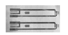
도 7은 실시예 1에 따른, 투명한 기재 상의 넓은 선폭을 갖는 전기 전도성 패턴의 이미지이다.
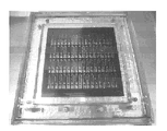
도 8은 실시예 1의 유리 마스터의 이미지이다.
도 9는 실시예 1에 따른, 유리 마스터를 위치시키고 PDMS 스탬프를 생성하기 위한 얕은 트레이의 이미지이다.
도면에서, 유사한 도면 부호는 유사한 요소를 지시한다. 축척에 맞게 작성되지 않을 수 있는 전술된 도면이 본 발명의 다양한 실시 형태를 개시하고 있지만, 발명을 실시하기 위한 구체적인 내용에 언급된 바와 같이, 다른 실시 형태가 또한 고려된다. 모든 경우에, 본 발명은 현재 개시되는 발명을 명백한 제한으로서가 아니라 예시적인 실시 형태의 표현으로서 기술한다. 본 발명의 범주 및 사상에 속하는 많은 다른 변형 및 실시 형태가 당업자에 의해 고안될 수 있음이 이해되어야 한다.BRIEF DESCRIPTION OF THE DRAWINGS The invention can be more fully understood by considering the following detailed description of various embodiments of the invention in conjunction with the accompanying drawings.
1 is a flow diagram illustrating a method of forming an electrically conductive pattern on a substrate, in accordance with one embodiment.
2 is a flow chart illustrating a method of forming a master tool having an ink pattern, according to one embodiment.
3 is a schematic diagram that provides a screen having a screen pattern, according to one embodiment.
Figure 4 is a schematic diagram of forming a master tool, according to one embodiment.
Figure 5 is a schematic view of forming a stamp, according to one embodiment.
6 is a schematic diagram of forming an electrically conductive pattern on a substrate, according to one embodiment.
7 is an image of an electrically conductive pattern having a wide line width on a transparent substrate, according to Example 1;
8 is an image of the glass master of Example 1. Fig.
9 is an image of a shallow tray for positioning a glass master and generating a PDMS stamp, according to embodiment 1;
In the drawings, like reference numerals designate like elements. While the foregoing drawings, which may not be drawn to scale, disclose various embodiments of the invention, other embodiments are also contemplated, as set forth in the Detailed Description for carrying out the invention. In all cases, the present invention describes the presently disclosed invention as an expression of an exemplary embodiment, not as obvious limitations. It should be understood that many other modifications and embodiments belonging to the scope and spirit of the invention may be devised by those skilled in the art.
본 발명은 기재 상에 넓은 선폭(예를 들어, 30 마이크로미터 이상)을 가진 전기 전도성 패턴 및 그의 형성 방법을 기재한다. 마스터 공구는 그의 주 표면 상에 잉크 패턴이 마련된다. 잉크 패턴은 스크린 인쇄 공정에 의해 형성된다. 스탬프-제조 재료를 마스터 공구의 주 표면에 적용하여, 마스터 공구의 잉크 패턴에 대해 네거티브인 스탬핑 패턴을 갖는 스탬프를 형성한다. 스탬핑 패턴의 스탬핑 표면에 잉크 조성물을 잉크칠하고 금속화된 표면과 접촉시켜, 스탬핑 패턴에 따라 금속화된 표면 상에 인쇄 패턴을 형성한다. 인쇄 패턴을 에칭 마스크로서 사용하여, 금속화된 표면을 에칭하여 전기 전도성 트레이스들을 형성한다.The present invention describes an electrically conductive pattern having a wide line width (e.g., greater than 30 micrometers) on a substrate and a method of forming the same. The master tool is provided with an ink pattern on its main surface. The ink pattern is formed by a screen printing process. The stamp-making material is applied to the master surface of the master tool to form a stamp having a negative stamping pattern with respect to the ink pattern of the master tool. The ink composition is inked on the stamping surface of the stamping pattern and brought into contact with the metallized surface to form a printed pattern on the metallized surface according to the stamping pattern. Using the print pattern as an etch mask, the metallized surface is etched to form electrically conductive traces.
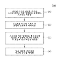
도 1은 일 실시 형태에 따른, 기재 상에 전기 전도성 패턴을 형성하는 방법(100)을 예시하는 흐름도이다. 110에서는, 잉크 패턴을 마스터 공구의 주 표면 상에 스크린-인쇄한다. 일부 실시 형태에서, 마스터 공구는, 예를 들어 유리 기재를 포함할 수 있다. 잉크 패턴은, 예를 들어 도 2에 도시된 방법(200)과 같은 스크린 인쇄 공정에 의해 형성되며, 이는 하기에 추가로 설명될 것이다. 이어서, 방법(100)은 120으로 진행한다.FIG. 1 is a flow chart illustrating a
120에서는, 스탬프-제조 재료를 마스터 공구의 주 표면 상의 잉크 패턴에 적용함으로써 스탬프를 형성한다. 스탬프는 잉크 패턴에 대해 네거티브인 스탬프 패턴을 갖는다. 일부 실시 형태에서, 스탬프-제조 재료는 하나 이상의 중합체 재료를 포함할 수 있다. 일부 실시 형태에서, 스탬프는 경화되지 않은 폴리다이메틸실록산(PDMS)을 마스터 공구에 적용하고, 이어서 경화시킴으로써 마스터 공구에 맞대어져 성형될 수 있다. 이어서, 방법(100)은 130으로 진행한다.At 120, a stamp is formed by applying the stamp-making material to the ink pattern on the master surface of the master tool. The stamp has a stamp pattern that is negative with respect to the ink pattern. In some embodiments, the stamp-making material may comprise one or more polymeric materials. In some embodiments, the stamp can be molded against the master tool by applying the uncured polydimethylsiloxane (PDMS) to the master tool and then curing. The
130에서는, 스탬프 패턴의 스탬핑 표면을 잉크 조성물로 잉크칠한다. 일부 실시 형태에서, 잉크 조성물은 금속화된 표면에 결합하도록 선택된 작용기를 포함하는 작용화 분자들을 포함할 수 있다. 이어서, 방법(100)은 140으로 진행한다.In 130, the stamped surface of the stamp pattern is inked with an ink composition. In some embodiments, the ink composition may comprise functionalizing molecules comprising functional groups selected to bind to the metallized surface. The
140에서는, 스탬핑 표면을 금속화된 표면과 접촉시켜, 그 위에 인쇄 패턴을 생성한다. 일부 실시 형태에서, 스탬프는 위치결정되고 금속화된 표면과 접촉하게 되고, 잉크의 패턴이 스탬프의 스탬핑 표면으로부터 금속화된 표면으로 전사되어, 그 위에 패턴화된 자기-집합된 단층(SAM)을 형성할 수 있다. 이어서, 방법(100)은 150으로 진행한다.At 140, the stamping surface is brought into contact with the metallized surface to create a printed pattern thereon. In some embodiments, the stamp is positioned and brought into contact with the metallized surface, and the pattern of ink is transferred from the stamped surface of the stamp to the metallized surface onto which a patterned self-assembled monolayer (SAM) . The
150에서는, 인쇄 패턴을 에칭 마스크로서 사용하여 금속화된 표면을 에칭함으로써 기재 상에 전기 전도성 트레이스들을 형성한다. 일부 실시 형태에서, 금속화된 표면은 기재 상에 배치된 전기 전도성 층일 수 있다. 전기 전도성 층은 패턴화된 SAM을 에칭 마스크로서 사용하여 에칭될 수 있다. 전기 전도성 층의 노출된 부분은 에칭함으로써 제거될 수 있고, 전기 전도성 층의 나머지 부분은 기재 상에 전기 전도성 패턴을 형성하는 전기 전도성 트레이스로서 현시될 수 있다.At 150, the electrically conductive traces are formed on a substrate by etching the metallized surface using a print pattern as an etch mask. In some embodiments, the metallized surface may be an electrically conductive layer disposed on a substrate. The electrically conductive layer may be etched using the patterned SAM as an etch mask. The exposed portion of the electrically conductive layer may be removed by etching, and the remainder of the electrically conductive layer may be exposed as an electrically conductive trace that forms an electrically conductive pattern on the substrate.
도 2는 마스터 공구, 예컨대 도 1의 방법(100)에 사용된 마스터 공구를 형성하는 방법(200)을 예시하는 흐름도이다. 210에서는, 스크린 상에 스크린 패턴이 마련된다. 스크린 패턴은 개방 영역들을 포함하며, 이러한 개방 영역들은 유체가 스크린을 통과할 수 있게 한다. 일부 실시 형태에서, 감광성 에멀젼 층이 스크린의 메시 구조물 상에 코팅될 수 있고, 감광성 에멀젼 층은 포토마스크를 통해 노출되어 미리 결정된 패턴을 형성할 수 있다. 감광성 에멀젼 층의 비노출된 영역이 씻겨 나가서 개방 영역들을 형성할 수 있다. 이어서, 방법(200)은 220으로 진행한다.2 is a flow chart illustrating a
220에서는, 스크린을 마스터 기재의 주 표면에 인접하게 위치시킨다. 일부 실시 형태에서, 마스터 기재는, 예를 들어 유리 기재일 수 있다. 이어서, 방법(200)은 230으로 진행한다.At 220, the screen is positioned adjacent to the main surface of the master substrate. In some embodiments, the master substrate may be, for example, a glass substrate. The
230에서는, 스크린의 개방 영역들을 통과하도록 잉크를 적용하여, 마스터 기재의 주 표면 상에 잉크 패턴을 형성한다. 일부 실시 형태에서, 잉크는, 예를 들어 세라믹 고온 잉크일 수 있으며, 이러한 세라믹 고온 잉크는 경화 또는 건조 후에 유리 기재에 단단히 접착될 수 있다. 이어서, 방법(200)은 240으로 진행한다.In 230, ink is applied to pass through the open areas of the screen to form an ink pattern on the main surface of the master substrate. In some embodiments, the ink may be, for example, a ceramic high temperature ink, and such ceramic high temperature ink may be firmly adhered to the glass substrate after curing or drying. The
240에서는, 잉크 패턴을 건조시켜 마스터 공구를 형성한다. 일부 실시 형태에서, 잉크 패턴은 마스터 기재의 주 표면으로부터 떨어져서 연장되는 잉크 패턴 요소들의 배열, 및 각각의 인접한 잉크 패턴 요소들 사이에 형성된 하나 이상의 오목부를 포함할 수 있다. 일부 실시 형태에서, 마스터 공구 상에 형성된 오목부들 중 적어도 하나는 측방향 치수가 30 마이크로미터 이상이고 깊이가 10 마이크로미터 이상이다.At 240, the ink pattern is dried to form the master tool. In some embodiments, the ink pattern may include an array of ink pattern elements extending away from the master surface of the master substrate, and at least one recess formed between each adjacent ink pattern element. In some embodiments, at least one of the recesses formed on the master tool has a lateral dimension of at least 30 micrometers and a depth of at least 10 micrometers.
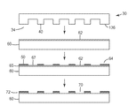
도 3은 일 실시 형태에 따른, 스크린 패턴을 갖는 스크린을 제공하는 개략도이다. 스크린(10)은 프레임(12) 및 프레임(12) 상에 장착된 메시 구조물(14)을 포함한다. 일부 실시 형태에서, 메시 구조물(14)은, 예를 들어 스테인리스강으로 제조된 와이어로부터 직조될 수 있다. 메시 구조물(14)은, 예를 들어 100 내지 1000의 메시 번호를 가질 수 있다. 에멀젼 층(16)을 메시 구조물(14)에 적용한다. 일부 실시 형태에서, 에멀젼 층(16)은 감광성 재료를 함유할 수 있으며, 이러한 감광성 재료에는, 예를 들어 폴리비닐아세테이트, 폴리 비닐 알코올, 아크릴레이트 단량체, 또는 이들의 조합이 포함된다. 에멀젼 층(16)의 두께는, 예를 들어 5 내지 100 마이크로미터, 10 내지 50 마이크로미터, 또는 15 내지 30 마이크로미터일 수 있다. 에멀젼 층(16)은 포토마스크(5)를 통해, 예를 들어 UV 광에 노출되어 미리 결정된 패턴을 형성한다. 노출된 영역(17a)들은 경화될 수 있고, 비노출된 영역들은 알려진 세정제에 의해 씻겨 나가서 개방 영역(17b)들을 형성할 수 있다. 경화된 영역(17a)들 및 개방 영역(17b)들은 스크린 패턴(17)을 형성한다. 스크린 패턴(17)을 갖는 스크린(10)은 적절한 재료를 사용하여 임의의 적절한 공정에 의해 형성될 수 있음이 이해되어야 한다.3 is a schematic diagram that provides a screen having a screen pattern, according to one embodiment. The
도 4는 일 실시 형태에 따른, 마스터 공구(20)를 형성하는 개략도이다. 도 3의 스크린(10)을 마스터 기재(22)의 주 표면(21)에 인접하게 위치시킨다. 주 표면(21)은 표면 조도(surface roughness)가, 예를 들어 50 마이크로미터 미만, 10 마이크로미터 미만, 2 마이크로미터 미만, 0.5 마이크로미터 미만, 또는 0.1 마이크로미터 미만일 수 있다. 잉크(6)를 스크린(10)에 적용하고, 스퀴지(7)를 미리 결정된 각도, 미리 결정된 속도, 및 밀 결정된 압력으로 스크린(10)을 가로질러 직행하여, 잉크(6)를 스퀴징하여 스크린(10)의 개방 영역(17b)들을 통과하여 마스터 기재(22) 상에 잉크 패턴(24)을 형성한다. 일부 실시 형태에서, 잉크(6)는 마스터 기재(22) 상에서 경화 또는 건조되어 잉크 패턴(24)을 형성할 수 있다. 일부 실시 형태에서, 마스터 기재(22)의 주 표면(21)은 잉크 패턴(24)과 마스터 기재(22) 사이의 결합을 개선하기 위해 화학물질로 개질될 수 있다. 일부 실시 형태에서, 마스터 기재(22)는, 예를 들어 사실상 평면인 표면을 갖는 유리 기재일 수 있고, 잉크(6)는, 예를 들어 세라믹 고온 잉크일 수 있는데, 이는, 예를 들어 약 700℃의 온도에서 경화 또는 건조 후에 유리 기재에 단단히 부착될 수 있다. 마스터 기재(22) 및 잉크(6)에 대한 재료들의 임의의 적절한 조합이, 잉크 패턴(24)이 그의 주 표면(21) 상에 형성될 수 있는 한, 사용될 수 있음이 이해되어야 한다.4 is a schematic diagram of forming a
잉크 패턴(24)은 주 표면(21)으로부터 떨어져서 연장되는 잉크 패턴 요소(24a)들의 배열 및 각각의 인접한 패턴 요소(24a)들 사이에 형성된 오목부(24b)들의 배열을 포함한다. 잉크 패턴 요소(24a)들 각각은 측방향 치수가, 예를 들어 10 마이크로미터 이상, 30 마이크로미터 이상, 50 마이크로미터 이상, 30 마이크로미터 내지 1 mm, 또는 50 내지 800 마이크로미터일 수 있다. 잉크 패턴 요소(24a)들 각각은 주 표면(21)에 대한 양각 높이가, 예를 들어 5 마이크로미터 이상, 10 마이크로미터 이상, 20 마이크로미터 이상, 10 내지 100 마이크로미터, 또는 10 내지 50 마이크로미터일 수 있다. 일부 실시 형태에서, 잉크 패턴 요소(24a)들은 주 표면(21)에 대한 드래프트각(draft angle) 또는 측벽각이, 예를 들어 0 내지 10도, 또는 0.5 내지 5도일 수 있다. 오목부(24b)들 각각은 하부 표면(26)을 가지며, 하부 표면은 마스터 기재(22)의 주 표면(21)의 노출된 부분이다. 오목부(24b)들 각각은 측방향 치수가, 예를 들어 10 마이크로미터 이상, 30 마이크로미터 이상, 50 마이크로미터 이상, 30 마이크로미터 내지 1 mm, 또는 50 내지 800 마이크로미터일 수 있다. 오목부(24b)들 각각은 잉크 패턴 요소(24a)들의 각각의 양각 높이에 상응하는 깊이를 가질 수 있다. 오목부(24b)들의 깊이는, 예를 들어 5 마이크로미터 이상, 10 마이크로미터 이상, 20 마이크로미터 이상, 10 내지 100 마이크로미터, 또는 10 내지 50 마이크로미터일 수 있다.The
본 명세서에 기재된 마스터 공구는 그 위에 잉크 패턴을 제공할 수 있으며, 잉크 패턴은 비교적 넓은 측방향 치수(예를 들어, 30 마이크로미터 이상) 및 비교적 큰 양각 높이 또는 깊이(예를 들어, 10 마이크로미터 이상)를 갖는 잉크 패턴 요소들 및 오목부들의 배열을 포함한다. 종래의 포토리소그래피 기법에 의해 제조된 마스터 공구 상의 포토레지스트 패턴은 일반적으로 훨씬 더 좁은 측방향 치수(예를 들어, 10 마이크로미터 이하) 및 훨씬 더 낮은 양각 높이(예를 들어, 1 마이크로미터 이하)를 갖는다.The master tool described herein may provide an ink pattern thereon and the ink pattern may have a relatively wide lateral dimension (e.g., greater than 30 micrometers) and a relatively greater raised height or depth (e.g., 10 micrometers Of the ink pattern elements and recesses. Photoresist patterns on master tools made by conventional photolithographic techniques generally have much narrower lateral dimensions (e.g., less than 10 micrometers) and much lower embossed heights (e.g., less than 1 micrometer) .
도 5는 일 실시 형태에 따른, 스탬프(30)를 형성하는 개략도이다. 도 4의 마스터 공구(20)를, 예를 들어 도 9에 도시된 바와 같은 얕은 트레이 안에 놓을 수 있다. 스탬프-제조 재료(32)의 층을 잉크 패턴(24) 상에 분배하여 잉크 패턴(24)의 네거티브를 형성한다. 스탬프-제조 재료(32)의 층을 경화에 의해 경질화하여 스탬프(30)를 형성할 수 있다. 스탬프(30)는 기부 표면(35) 및 기부 표면(35)으로부터 떨어져서 연장되는 패턴 요소(36)들의 배열을 포함한다. 기부 표면(35)은 사실상 평면일 수 있다. 일부 실시 형태에서, 스탬프(30)는 탄성중합체성 재료의 단일형 블록(unitary block)일 수 있고, 다른 실시 형태에서는 선택적인 보강 배킹 층에 의해 지지된 패턴 요소(36)들을 포함할 수 있다. 스탬프(30)의 기부 표면(35) 상의 패턴 요소(36)들의 어레이는 스탬핑 패턴(34)을 형성하며, 스탬핑 패턴은 의도된 미세접촉 인쇄 적용에 따라 폭넓게 변동될 수 있고, 예를 들어 요소들의 규칙 또는 불규칙 패턴, 예컨대 라인, 도트, 다각형 등을 포함할 수 있다.5 is a schematic view of forming a
스탬프-제조 재료(32)는, 예를 들어 단일중합체, 공중합체 등을 포함한 하나 이상의 중합체 재료를 포함할 수 있다. 스탬프(30)의 제조에 사용하기에 적합한 중합체 재료는, 예를 들어 실리콘, 폴리우레탄, 에틸렌 프로필렌 다이엔 M-클래스(EPDM) 고무뿐만 아니라, 구매가능한 플렉소(flexographic) 인쇄 플레이트 재료(예를 들어, 미국 델라웨어주 윌밍턴 소재의 이. 아이. 듀폰 디 네모아 앤드 컴퍼니(E. I. du Pont de Nemours and Company)로부터 상표명 사이렐(Cyrel)로 구매가능한 것들)을 포함할 수 있다. 스탬프는, 예를 들어, 직포 또는 부직포 섬유질 보강재와 조합된 스탬핑 표면(136) 상의 탄성중합체성 재료를 포함한 복합 재료로부터 제조될 수 있다.The stamp-making
폴리다이메틸실록산(PDMS)이 스탬프 재료로서 특히 유용한데, 왜냐하면 그것이 탄성중합체성이고, 저 표면 에너지(이는 대부분의 기재로부터 스탬프를 제거하는 것을 용이하게 함)를 갖기 때문이다. 유용한 구매가능한 제형이 미국 미시간주 미들랜드 소재의 다우 코닝(Dow Corning)으로부터 상표명 실가드(Sylgard) 184 PDMS로 입수가능하다. PDMS 스탬프는, 예를 들어 비가교결합된 PDMS 중합체를, 예를 들어 잉크 패턴(24)과 같은 패턴화된 몰드 내로 또는 그를 향하여 분배한 후, 경화시킴으로써 형성될 수 있다. 탄성중합체성 스탬프를 성형하기 위한 마스터 공구는 상기 도 4에 예시된 바와 같은 공정에 의해 형성될 수 있다. 탄성중합체성 스탬프는 경화되지 않은 PDMS를 마스터 공구(20)에 적용하고, 이어서 경화시킴으로써 마스터 공구(20)에 맞대어져 성형될 수 있다.Polydimethylsiloxane (PDMS) is particularly useful as a stamping material because it is elastomeric and has low surface energy (which facilitates removing stamps from most substrates). A useful commercially available formulation is available under the tradename Sylgard 184 PDMS from Dow Corning, Midland, Michigan. The PDMS stamp may be formed, for example, by dispensing the non-crosslinked PDMS polymer into or into a patterned mold such as, for example,
기부 표면(35) 상의 어레이를 이룬 패턴 요소(36)들은 그들의 형상, 배향, 및 크기의 관점에서 설명될 수 있다. 패턴 요소(36)들 각각은 스탬핑 표면(136)을 포함하는데, 스탬핑 표면은 도 4에 도시된 바와 같은 마스터 공구(20) 상의 오목부(24b)들의 하부 표면(26)에 따라 형성된다. 스탬핑 표면(136)은 기부 표면(35) 위로 높이(h)가 존재하고, 측방향 치수(w)를 갖는다. 일부 실시 형태에서, 측방향 치수(w)는, 예를 들어 10 마이크로미터 이상, 30 마이크로미터 이상, 50 마이크로미터 이상, 30 마이크로미터 내지 1 mm, 또는 50 내지 800 마이크로미터일 수 있다. 높이(h)는, 예를 들어 5 마이크로미터 이상, 10 마이크로미터 이상, 20 마이크로미터 이상, 10 내지 100 마이크로미터, 또는 20 내지 50 마이크로미터일 수 있다. 인접한 패턴 요소(36)들 사이의 간격(l)은, 예를 들어 10 마이크로미터 이상, 30 마이크로미터 이상, 50 마이크로미터 이상, 30 마이크로미터 내지 1 mm, 또는 50 내지 800 마이크로미터일 수 있다.The arrayed
패턴 요소(36)들은 기부 표면(35)의 전부 또는 단지 일부만을 점유할 수 있다. 일부 실시 형태에서, 미세접촉 인쇄를 위한 패턴 요소(36)들의 어레이는 스탬프(30)의 기부 표면(35) 상의, 예를 들어 100 ㎠ 초과, 400 ㎠ 초과, 또는 심지어 1000 ㎠ 초과의 면적을 덮을 수 있다. 일부 실시 형태에서, 패턴 요소(36)들은 "미세패턴", 예를 들어 스탬핑 패턴(34)을 형성할 수 있으며, 이것은 본 출원에서, 예를 들어 도트, 라인, 채워진 형상, 또는 이들의 조합의 배열을 지칭할 수 있다. 일부 실시 형태에서, 패턴 요소(36)들은 트레이스들 - 이것은 직선 또는 곡선형일 수 있음 - 을 포함할 수 있으며, 이러한 트레이스들은 2차원 네트워크(예를 들어, 메시 또는 회로)를 형성할 수 있다.The
도 6은 일 실시 형태에 따른, 기재 상에 전기 전도성 패턴을 형성하는 개략도이다. 작용화 분자를 포함하는 잉크(40)가 스탬프(30)의 스탬핑 표면(136)들 상에 존재한다. 잉크(40) 내의 작용화 분자는 기재(60) 상의 재료 표면(62)에 결합하도록 선택된 작용기를 포함할 수 있다. 스탬프(30)를 위치결정하고 재료 표면(62)과 접촉하게 하고, 스탬핑 표면(136)들을 재료 표면(62)의 제1 부분(65)에 대고 유지한다. 잉크(40) 내의 작용화 분자를 재료 표면(62)에 대고 유지하여 작용기가 거기에 결합될 수 있게 한다. 이어서, 스탬핑 표면(136)들을 제거하고, 재료 표면(62) 상에 남아 있는 잉크는 표면에 화학적으로 결합할 수 있고, 스탬핑 표면(136)들의 형상 및 치수에 따라 재료 표면(62)의 제1 부분(65)들 상에 자기-집합된 단층(SAM)(50)을 형성한다. 제1 부분(65)들과 인접한, 재료 표면(62)의 부분(67)들이 SAM(50)이 없는 상태로 남아 있다. 이러한 방식으로, 잉크(40)의 패턴이 스탬프(30) 상의 스탬핑 표면(136)으로부터 기재(60)의 재료 표면(62)에 전사될 수 있다. 전사된 패턴은, SAM(50)들의 배열을 포함하고 스탬프(30)의 스탬핑 패턴(34)에 상응하는 인쇄 패턴(64)으로서 예시되어 있다.6 is a schematic diagram of forming an electrically conductive pattern on a substrate, according to one embodiment. An
도 6의 실시 형태에서, 재료 표면(62)은 기재(60)의 금속화된 표면일 수 있다. 재료 표면(62)은, 예를 들어 기재(62)의 표면 상에 전기 전도성 층을 제공함으로써 형성될 수 있다. SAM(50)들을 지지하기 위한 전기 전도성 층(62)은, 예를 들어 금, 은, 팔라듐, 백금, 로듐, 구리, 니켈, 철, 인듐, 주석, 탄탈, 알루미늄뿐만 아니라, 이들 원소의 혼합물, 합금, 및 화합물을 포함할 수 있다. 전기 전도성 층은 임의의 적합한 전기 전도성 재료를 포함할 수 있는 것으로 이해되어야 한다. 일 실시 형태에서, 전기 전도성 층은 복합 재료, 예를 들어 금속-충전된 중합체를 포함할 수 있다. 기재(60) 상의 전기 전도성 층은, 예를 들어 약 10 나노미터(nm) 내지 약 100 마이크로미터와 같은 임의의 두께일 수 있다. 전기 전도성 층은 임의의 편리한 방법, 예를 들어 스퍼터링, 증발, 화학 증착, 또는 화학 용액 침착(무전해 도금을 포함함)을 사용하여 침착될 수 있다.In the embodiment of FIG. 6, the
일부 실시 형태에서, 재료 표면(62)은 기재(60) 상에 배치된 코팅 층일 수 있다. 코팅 층의 재료는, 예를 들어 원소 금속, 금속 합금, 금속간 화합물, 금속 산화물, 금속 황화물, 금속 탄화물, 금속 질화물, 및 이들의 조합을 포함할 수 있다.In some embodiments,
재료 표면(62) 및 잉크(40)는 그 안의 작용화 분자가 기재(60) 상의 재료 표면(62)에 결합하는 작용기를 포함하도록 선택된다. 작용기는 작용화 분자의 물리적 말단뿐만 아니라, 분자종이 SAM(50)을 형성할 수 있는 방식으로 재료 표면(26)과의 결합을 형성하는 데 이용가능한 분자의 어느 부분에도 또는 분자가 SAM 형성에 관여될 때 노출된 채로 남아 있는 분자의 어느 부분에도 존재할 수 있다. 일부 실시 형태에서, 잉크(40) 내의 작용화 분자는 스페이서 부분에 의해 분리된 제1 및 제2 종결 말단을 갖는 것으로 여겨질 수 있으며, 제1 종결 말단은 재료 표면(62)에 결합하도록 선택된 작용기를 포함하고, 제2 말단기는 선택적으로, 바람직한 노출된 작용기를 갖는 재료 표면(62) 상에 SAM(50)을 제공하도록 선택된 작용기를 포함한다. 분자의 스페이서 부분은 생성된 SAM(50)의 특정 두께를 제공하도록 할 뿐만 아니라, SAM(50)의 형성을 촉진하도록 선택될 수 있다. 본 명세서에 기재된 실시 형태에서의 SAM(50)은 두께가 다양할 수 있지만, 두께가 약 5 나노미터 미만인 SAM(50)이 대체로 바람직하며, 더 바람직하게는 두께가 약 3 나노미터 미만인 것들, 그리고 더 바람직하게는 두께가 약 1.5 나노미터 미만인 것들이다. 이들 치수는 일반적으로 분자종, 및 특히 그의 스페이서 부분의 선택에 의해 좌우된다.The
일부 실시 형태에서, 기재(60) 상의 재료 표면(62) 상에 형성된 SAM(50)은 다양한 목적으로 그러한 형성 후에 개질될 수 있다. 예를 들어, 잉크(40) 내의 작용화 분자가 SAM(50) 상태로 재료 표면(62) 상에 침착될 수 있고, 작용화 분자는 노출된 작용기를 갖는데, 이러한 작용기에는 보호기가 포함되며, 이는 SAM(50)의 추가의 개질을 달성하기 위해 제거될 수 있다. 대안적으로, 반응성 기가 잉크(40) 내의 작용화 분자의 노출된 부분 상에 제공될 수 있으며, 이것은 전자 빔 리소그래피, X-선 리소그래피, 또는 임의의 다른 방사선에 의해 활성화 또는 불활성화될 수 있다. 그러한 보호 및 탈보호는 기존의 표면-결합된 SAM(50)의 화학적 또는 물리적 개질에 도움이 될 수 있다.In some embodiments, the
일부 실시 형태에서, 코팅 층(62)의 재료들과 잉크(40) 내의 작용화 분자에 대한 작용기의 조합은, 예를 들어 하기를 포함할 수 있다: (1) 금, 은, 구리, 카드뮴, 아연, 팔라듐, 백금, 수은, 납, 철, 크롬, 망간, 텅스텐, 및 이들의 임의의 합금과 같은 금속과 티올, 황화물, 이황화물 등과 같은 황-함유 작용기; (2) 도핑된 또는 비도핑된 규소와 실란 및 클로로실란; (3) 실리카, 알루미나, 석영, 유리 등과 같은 금속 산화물과 카르복실산; (4) 백금 및 팔라듐과 니트릴 및 아이소니트릴; 및 (4) 구리와 하이드록삼산. 잉크(40) 내의 작용화 분자 상의 추가의 적합한 작용기는 산 염화물, 무수물, 설포닐 기, 포스포릴 기, 하이드록실 기 및 아미노산 기를 포함한다. 추가의 표면 재료는 게르마늄, 갈륨, 비소, 및 비소화갈륨을 포함한다. 추가적으로, 에폭시 화합물, 폴리설폰 화합물, 플라스틱 및 다른 중합체가 재료 표면(62)을 위한 재료로서 사용될 수 있다.In some embodiments, the combination of the materials of the
일부 실시 형태에서, 본 명세서에 기재된 실시 형태에서 SAM(50)을 형성하는 데 이용되는 작용화 분자는 미국 특허 출원 공개 제2010/0258968호에 기재된 바와 같은 하나 이상의 유기황 화합물을 포함하는 잉크(40)로서 스탬프(30)에 전달된다. 각각의 유기황 화합물은 바람직하게는 재료 표면(62)의 선택된 부분(65) 상에 SAM(50)을 형성할 수 있는 티올 화합물이다. 티올은 --SH 작용기를 포함하고, 메르캅탄으로도 불릴 수 있다. 티올 기는 잉크(40) 내의 작용화 화합물의 분자와 재료 표면(62), 예를 들어 금속 표면 사이의 화학 결합을 생성하는 데 유용하다. 유용한 티올은, 예를 들어 알킬 티올 및 아릴 티올을 포함할 수 있다. 다른 유용한 유기황 화합물은, 예를 들어 다이알킬 다이설파이드, 다이알킬 설파이드, 알킬 잔테이트, 다이티오포스페이트, 및 다이알킬티오카르바메이트를 포함할 수 있다.In some embodiments, the functionalizing molecules used to form the
일부 실시 형태에서, 잉크(40)는 알킬 티올, 예컨대 선형 알킬 티올: HS(CH2)nX를 포함할 수 있으며, 여기서 n은 메틸렌 단위의 수이고, X는 알킬 사슬의 말단기(예를 들어, X = --CH3, --OH, --COOH, --NH2 등)이다. 바람직하게는, X = --CH3이다. 다른 유용한 작용기는, 예를 들어 (1) 문헌[Ulman, "Formation and Structure of Self-Assembled Monolayers", Chemical Reviews Vol. 96, pp. 1533-1554 (1996)]; 및 (2) 문헌[Love et al., "Self-Assembled Monolayers of Thiolates on Metals as a Form of Nanotechnology", Chemical Reviews Vol. 105, pp. 1103-1169 (2005)]에 기재된 것들을 포함한다.In some embodiments, the
유용한 알킬 티올은 선형 알킬 티올(즉, 직쇄 알킬 티올) 또는 분지형일 수 있고, 치환되거나 비치환될 수 있다. 이러한 선택적인 치환체는 바람직하게는 SAM의 형성을 방해하지 않는다. 유용한 분지형 알킬 티올의 예에는 메틸 기가 선형 알킬 사슬 주쇄의 매 세 번째 또는 매 네 번째마다의 탄소 원자에 부착된 알킬 티올(예를 들어, 피타닐티올)이 포함된다. 유용한 알킬 티올 내의 중쇄 치환체의 예에는 에테르기 및 방향족 고리가 포함된다. 유용한 티올은 또한 3차원 환형 화합물(예를 들어, 1-아다만탄티올)을 포함할 수 있다. 바람직한 선형 알킬 티올은 10 내지 20개의 탄소 원자(더 바람직하게는, 12 내지 20개의 탄소 원자; 가장 바람직하게는 16개의 탄소 원자, 18개의 탄소 원자, 또는 20개의 탄소 원자)를 갖는다.Useful alkylthiols may be linear alkylthiol (i.e., straight chain alkylthiol) or branched and may be substituted or unsubstituted. This optional substituent preferably does not interfere with the formation of the SAM. Examples of useful branched alkylthiols include alkylthiols (e.g., pthanylthiol) in which the methyl group is attached to every third or every fourth carbon atom of the linear alkyl chain backbone. Examples of heavy chain substituents in useful alkylthiols include ether groups and aromatic rings. Useful thiols may also include a three-dimensional cyclic compound (e. G., 1-adamantanetiol). Preferred linear alkylthiols have from 10 to 20 carbon atoms (more preferably 12 to 20 carbon atoms; most preferably 16 carbon atoms, 18 carbon atoms, or 20 carbon atoms).
적합한 알킬 티올은 구매가능한 알킬 티올(미국 위스콘신주 밀워키 소재의 알드리치 케미칼 컴퍼니(Aldrich Chemical Company))을 포함할 수 있다. 바람직하게는, 잉크 용액(20)은 용매 및 유기황 화합물로 주로 이루어지며, 이때 불순물은 잉크 용액의 약 5 중량% 미만; 더 바람직하게는 약 1 중량% 미만; 훨씬 더 바람직하게는 약 0.1 중량% 미만을 구성한다. 유용한 잉크(20)는, 예를 들어 알킬 티올과 다이알킬 다이설파이드의 혼합물과 같은, 공통 용매 중에 용해된 상이한 유기황 화합물들의 혼합물을 함유할 수 있다.Suitable alkyl thiols may include commercially available alkyl thiols (Aldrich Chemical Company, Milwaukee, Wis.). Preferably, the
방향족 고리에 부착된 티올 기를 포함하는 아릴 티올이 또한 잉크(40)에 유용하다. 유용한 아릴 티올의 예에는 바이페닐 티올 및 테르페닐 티올이 포함된다. 바이페닐 및 테르페닐 티올은 다양한 위치들 중 임의의 위치에서 하나 이상의 작용기로 치환될 수 있다. 유용한 아릴 티올의 다른 예에는, 작용기로 치환될 수 있거나 치환되지 않을 수 있는 아센 티올이 포함된다. 일부 실시 형태에서, 유용한 티올은 선형 공액(conjugated) 탄소-탄소 결합, 예를 들어 이중 결합 또는 삼중 결합을 포함할 수 있고, 부분 또는 완전 플루오르화될 수 있다.Arylthiol containing a thiol group attached to the aromatic ring is also useful in the
잉크(40)는 2가지 이상의 화학적으로 별개인 유기황 화합물을 포함할 수 있다. 예를 들어, 잉크는 상이한 사슬 길이를 각각 갖는 2가지 선형 알킬 티올 화합물을 포함할 수 있다. 다른 예로서, 잉크(40)는 상이한 꼬리 기(tail group)를 갖는 2가지 선형 알킬 티올 화합물을 포함할 수 있다.The
미세접촉 인쇄가 스탬프를 잉크칠하기 위해 순수(neat) 유기황 화합물을 사용하여 수행되어 왔지만, 스탬프에의 유기황 화합물의 전달은, 용매-기반 잉크로부터 전달된다면, 더 균일하게, 그리고 선형 알킬 티올 및 PDMS 스탬프의 경우에 더 덜한 스탬프 팽윤(swelling)을 갖고서 달성될 수 있다. 일부 실시 형태에서, 잉크(40)는 하나 초과의 용매를 포함할 수 있지만, 가장 유용한 제형은 단지 단일 용매만을 포함할 필요가 있다. 단지 하나의 용매로 제형화된 잉크는 소량의 불순물 또는 첨가제, 예를 들어 안정제 또는 건조제(desiccant)를 함유할 수 있다.Although fine contact printing has been carried out using neat organosulfur compounds to ink stamps, the transfer of the organosulfur compounds to the stamp is more uniformly carried out and more efficient when applied from a solvent-based ink, And less stamp swelling in the case of PDMS stamps. In some embodiments, the
유용한 용매는 바람직하게는 미세접촉 인쇄를 위해 가장 흔히 사용되는 스탬프 재료인 PDMS와 양립할 수 있다(즉, 그것은 PDMS를 과도하게 팽윤시키지 않음). 미세접촉 인쇄에서, PDMS 스탬프의 팽윤은 패턴화된 특징부의 뒤틀림 및 불량한 패턴 충실도를 초래할 수 있다. 잉크칠 접근법에 따라, 과도한 팽윤은 또한 스탬프에 대한 기계적 지지를 제공함에 있어서 상당한 문제를 일으킬 수 있다.Useful solvents are preferably compatible with PDMS, which is the most commonly used stamping material for micro-contact printing (i.e., it does not over-swell the PDMS). In fine contact printing, swelling of the PDMS stamp can lead to distortion of the patterned features and poor pattern fidelity. In accordance with the inking approach, excessive swelling can also cause significant problems in providing mechanical support for the stamp.
케톤이 잉크 용액에 적합한 용매일 수 있다. 일부 실시 형태에서, 적합한 용매는 예를 들어 아세톤, 메틸 에틸 케톤, 에틸 아세테이트 등, 및 이들의 조합을 포함한다. 아세톤이 특히 바람직한 용매이다. 하나 이상의 유기황 화합물(예를 들어, 티올 화합물)이 용매 내에 약 3 밀리몰(mM) 이상의 총 농도로 존재한다. 본 명세서에 사용된 바와 같이, "총 농도"는 합계해서 취해진 모든 용해된 유기황 화합물의 몰 농도를 말한다. 하나 이상의 유기황 화합물(예를 들어, 티올 화합물)은 잉크 용액이 단일 상으로 본질적으로 이루어지는 임의의 총 농도로 존재할 수 있다. 하나 이상의 유기황 화합물(예를 들어, 티올 화합물)은 약 5 mM 이상, 약 10 mM 이상, 약 20 mM 이상, 50 mM 이상, 그리고 심지어 약 100 mM 이상의 총 농도로 존재할 수 있다.Ketones can be suitable for ink solutions every day. In some embodiments, suitable solvents include, for example, acetone, methyl ethyl ketone, ethyl acetate, and the like, and combinations thereof. Acetone is a particularly preferred solvent. At least one organic sulfur compound (e.g., a thiol compound) is present in the solvent at a total concentration of at least about 3 millimoles (mM). As used herein, "total concentration" refers to the molar concentration of all dissolved organic sulfur compounds taken together in total. One or more organic sulfur compounds (e.g., thiol compounds) may be present in any total concentration at which the ink solution essentially consists of a single phase. More than one organosulfur compound (e.g., a thiol compound) may be present at a total concentration of greater than about 5 mM, greater than about 10 mM, greater than about 20 mM, greater than 50 mM, and even greater than about 100 mM.
스탬프(30)는 (예를 들어, 문헌[Libioulle et al. "Contact-Inking Stamps for Microcontact Printing of Alkanethiols on Gold", Langmuir Vol. 15, pp. 300-304 (1999)]에 기재된 바와 같은) 당업계에 알려진 방법을 사용하여 본 명세서에 기재된 실시 형태의 잉크(40)로 "잉크칠"될 수 있다. 한 가지 접근법에서는, 잉크(40)가 함침된 어플리케이터(applicator)(예를 들어, 면봉(cotton swab) 또는 폼 어플리케이터)를 스탬프(30)의 스탬핑 표면(136)을 가로질러 문지른 후에, 스탬핑 표면(136)으로부터의 용매의 건조를 수행할 수 있다. 다른 접근법에서는, 스탬핑 표면(136)을 잉크 용액이 함침된 "잉크 패드"에 대해 가압할 수 있으며, 이때 잉크 패드는 선택적으로 PDMS 슬래브(slab)이다. 다른 접근법에서는, 스탬프를, 인쇄 표면에 대해, 그것의 배면으로부터 잉크 용액으로 충전시킬 수 있다. 후자의 접근법에서는, 유기황 화합물이 스탬프(30)를 통해 확산되어 인쇄를 위한 양각-패턴화된 면(face)에 도달한다. 다른 실시 형태에서는, 스탬프(30)의 양각-패턴화된 인쇄 면을 잉크 용액 중에 침지한 후에, 인출 및 건조를 수행할 수 있다("침지식 잉크칠").
다시 도 6을 참조하면, 재료 표면(62)(예를 들어, 전기 전도성 층)을 SAM(50)들을 에칭 마스크로서 사용하여 에칭하여 노출된 부분(67)을 제거한다. 전기 전도성 층의 노출된 부분(67)의 제거는, 예를 들어 건식 에칭, 또는 습식 화학 에칭을 포함한 임의의 적절한 공정을 통해 달성될 수 있음이 이해되어야 한다. 에칭 후에, 전기 전도성 트레이스(72)들이 기재(60) 상에 형성된다. 전기 전도성 트레이스(72)들은 SAM(50)들에 의해 덮여진 전기 전도성 층의 제1 부분(65)들에 상응한다.Referring again to FIG. 6, material surface 62 (e.g., an electrically conductive layer) is etched using
일부 실시 형태에서, 전기 전도성 트레이스(72)들 중 적어도 하나는 측방향 치수가, 예를 들어 10 마이크로미터 이상, 30 마이크로미터 이상, 50 마이크로미터 이상, 30 마이크로미터 내지 1 mm, 또는 50 내지 800 마이크로미터이다. 기재(60) 상의 전기 전도성 트레이스(72)들은, 예를 들어 약 10 나노미터(nm) 내지 약 100 마이크로미터와 같은 임의의 두께일 수 있다. 전기 전도성 트레이스(72)들은 기재(60) 상에 전기 전도성 패턴(70)을 형성한다. 남아 있는 SAM(50)들은 기재(60)로부터 씻겨 나가서 전기 전도성 패턴(70)을 현시할 수 있다.In some embodiments, at least one of the electrically conductive traces 72 has a lateral dimension of, for example, 10 micrometers or more, 30 micrometers or more, 50 micrometers or more, 30 micrometers to 1 mm, or 50 to 800 Micrometer. The electrically conductive traces 72 on the
기재(60)는, 예를 들어 중합체 필름, 유리, 실리콘 웨이퍼 등을 포함할 수 있다. 일부 실시 형태에서, 기재(60)는, 편평한 시트의 형태이며 롤-투-롤(roll-to-roll) 방식으로 처리하기에 충분히 가요성이고 강한 중합체 필름일 수 있다. 본 명세서에 기재된 물품에서 기재로서 사용되는 중합체 필름은 때때로 베이스 필름으로 지칭된다. 롤-투-롤이란, 재료가 지지체 상에 감기거나 그로부터 풀릴 뿐만 아니라 어떤 방식으로 추가 처리되는 공정을 의미한다. 추가 처리의 예에는 코팅, 슬리팅(slitting), 블랭킹(blanking) 및 방사선에의 노출 등이 포함된다. 중합체 필름은, 일반적으로, 예를 들어, 5 마이크로미터 내지 1000 마이크로미터의 범위의 다양한 두께로 제조될 수 있다. 일부 실시 형태에서, 중합체 필름 두께는 25 마이크로미터 내지 500 마이크로미터, 또는 50 마이크로미터 내지 250 마이크로미터, 또는 75 마이크로미터 내지 200 마이크로미터의 범위이다. 롤-투-롤 중합체 필름은 폭이 12 인치, 24 인치, 36 인치, 또는 48 인치 이상일 수 있다. 중합체 필름은, 예를 들어 폴리(에틸렌 테레프탈레이트)(PET), 폴리(부틸렌 테레프탈레이트)(PBT), 폴리(에틸렌 나프탈레이트)(PEN), 폴리카르보네이트, 셀룰로스 트라이아세테이트 등을 포함할 수 있다. 일부 실시 형태에서, 기재(60)는 PET, PBT, PEN, 또는 이들의 조합을 포함할 수 있다.The
일부 실시 형태에서, 기재(60)는 가요성 기재일 수 있으며, 여기서 가요성 기재 재료는 롤-투-롤 방식으로 가공하기에 충분히 가요성이고 강한 편평한 시트 또는 웨브의 형태의 중합체 재료인 중합체 필름일 수 있다. 일부 실시 형태에서, 중합체 필름 웨브는 표면 상에 비교적 얇은 금속 코팅을 포함하며, 금속 코팅에는 스탬프로부터의 잉크가 적용될 것이다. 금속 코팅은 의도된 응용에 따라 폭넓게 변동될 수 있지만, 웨브가 상기에 규정된 바와 같이 그의 가요성을 보유하도록 하기에 충분히 얇아야 한다.In some embodiments, the
본 명세서에 기재된 일부 실시 형태는 스크린 인쇄 공정에 의해 제조될 수 있는 마스터 공구를 제공한다. 본 명세서에 기재된 일부 마스터 공구, 예를 들어 도 4에서의 마스터 공구(20)는, 양각 높이가 10 마이크로미터 이상이고, 측방향 치수가 30 마이크로미터 이상인 패턴 요소들을 제공할 수 있다. 마스터 공구는 스탬프, 예컨대 특징적인 높이가 10 마이크로미터 이상이고 측방향 치수가 30 마이크로미터 이상인 하나 이상의 스탬핑 패턴 요소들을 갖는 도 5에서의 스탬프(30)를 형성하기 위해 사용될 수 있다. 본 명세서에 제공된 일부 스탬프는 미세접촉 인쇄에 의해 기재 상에 고품질 인쇄 패턴을 생성하기 위해 사용될 수 있다. 예를 들어, 스탬핑 패턴 요소들은 비교적 높기 때문에(예를 들어, 10 마이크로미터 이상), 스탬핑 패턴 요소들의 변형으로 인해 가능한 에지 블러링(edge blurring)이 효과적으로 피해질 수 있다. 대조적으로, 본 발명에서 달성된 바와 같은 높은 양각 높이 및 넓은 측방향 치수를 얻기 위해 종래의 포토리소그래피 기법으로 포토레지스트 패턴(예를 들어, 미국 특허 제5,512,131호에서의 규소 상의 포토레지스트 패턴)을 제조하는 것은 기술적으로 어렵고, 시간-소모적이고, 비용이 많이 든다. 비교적 낮은 양각 높이(예를 들어, 1 마이크로미터 이하)를 갖는 포토레지스트 패턴을 사용하는 경우, 미세접촉 인쇄를 통해, 트레이스들의 에지의 블러링 없이 넓은 선폭(예를 들어, 30 마이크로미터 이상)으로 기재 상에 트레이스들을 생성하는 것은 기술적으로 어려울 것이다.Some embodiments described herein provide a master tool that can be manufactured by a screen printing process. Some of the master tools described herein, for example the
본 명세서의 전체에 걸쳐 "일 실시 형태", "소정 실시 형태", "하나 이상의 실시 형태" 또는 "실시 형태"에 대한 언급은, 용어 "실시 형태"에 선행하는 용어 "예시적인"을 포함하든 포함하지 않든 간에, 그 실시 형태와 관련하여 설명된 특정한 특징, 구조, 재료 또는 특성이 본 발명의 소정의 예시적인 실시 형태들 중 적어도 하나의 실시 형태에 포함됨을 의미한다. 따라서, 본 명세서 전체에 걸쳐 다양한 곳에서의 "하나 이상의 실시 형태에서", "소정 실시 형태에서", "일 실시 형태에서" 또는 "실시 형태에서"와 같은 어구의 표현은 반드시 본 발명의 소정의 예시적인 실시 형태들 중 동일한 실시 형태를 언급하는 것은 아니다. 더욱이, 특정한 특징, 구조, 재료, 또는 특성은 하나 이상의 실시 형태에서 임의의 적합한 방식으로 조합될 수 있다.Reference throughout this specification to "one embodiment", "an embodiment", "one or more embodiments" or "an embodiment" means that the term "exemplary" Means that a particular feature, structure, material, or characteristic described in connection with the embodiment is included in at least one of the exemplary exemplary embodiments of the present invention. Thus, the appearances of the phrases "in one or more embodiments," in certain embodiments, "in an embodiment," or "in an embodiment," But does not refer to the same embodiment among the exemplary embodiments. Furthermore, a particular feature, structure, material, or characteristic may be combined in any suitable manner in one or more embodiments.
실시예Example
실시예(들)는 단지 예시를 위한 것이며 첨부된 청구범위의 범주를 과도하게 제한하기 위한 것이 아니다. 본 발명의 넓은 범주를 기재하는 수치 범위 및 파라미터가 근사치임에도 불구하고, 구체적인 실시예에 기재된 수치 값은 가능한 한 정확하게 기록된다. 그러나, 임의의 수치는 본래, 그의 각각의 시험 측정에서 발견되는 표준 편차로 인해 필연적으로 생기는 특정 오차를 포함한다. 최소한으로, 그리고 청구범위의 범주에 대한 균등론의 적용을 제한하려는 시도로서가 아니라, 각각의 수치 파라미터는 적어도 보고된 유효숫자의 개수의 관점에서 그리고 보통의 반올림 기법을 적용함으로써 해석되어야 한다.The embodiment (s) is for illustrative purposes only and is not intended to unduly limit the scope of the appended claims. Notwithstanding that the numerical ranges and parameters setting forth the broad scope of the invention are approximations, the numerical values set forth in the specific examples are recorded as precisely as possible. However, any numerical value inherently includes certain errors necessarily resulting from the standard deviation found in its respective test measurements. At the very least, and not as an attempt to limit the application of the doctrine of equivalents to the scope of the claims, each numerical parameter should at least be construed in light of the number of reported significant digits and by applying ordinary rounding techniques.
실시예 1Example 1
도 7에 도시된 바와 같이, 표면 상에 은 금속 패턴을 갖는 예시적인 PET 필름을 하기의 가공 단계에 의해 제조하였다:As shown in Figure 7, an exemplary PET film having a silver metal pattern on its surface was prepared by the following processing steps:
(1) 스크린에 스테인리스강으로 제조된 와이어로부터 직조된 메시 구조물을 마련한다. 메시 구조물은 크기가 65 cm × 75 cm이고, 메시 번호가 400이다. 두께가 약 20 마이크로미터인 광감성 에멀젼을 메시 구조물 상에 코팅하였다. 감광성 에멀젼은 타이완 소재의 마티나 컴퍼니(Matina Co.)로부터 구매가능하다. 감광성 에멀젼을 UV 광에 노출시켜, 인쇄되는 영역들로 이루어진 패턴 개구들을 생성하였다. 패턴 개구들은 최소 선폭이 약 0.4 mm이다.(1) Provide a woven mesh structure from the wire made of stainless steel on the screen. The mesh structure is 65 cm x 75 cm in size and has a mesh number of 400. A light-emissive emulsion having a thickness of about 20 micrometers was coated on the mesh structure. The photosensitive emulsion is available from Matina Co., Taiwan. The photosensitive emulsion was exposed to UV light to create patterned apertures of printed areas. The pattern openings have a minimum line width of about 0.4 mm.
(2) 세라믹 고온 잉크를 단계 1의 스크린을 통해 유리 기재 상에 스크린-인쇄하여, 도 8에 도시된 바와 같은 잉크 패턴을 갖는 유리 마스터를 형성한다. 유리 기재는 크기가 205 mm × 195 mm이고 두께가 4.75 내지 4.77 mm이다. 잉크를 약 700℃의 온도에서 건조시켰다. 건조된 잉크 패턴은 두께가 약 10 내지 약 12 마이크로미터이다.(2) Ceramic hot ink is screen-printed on the glass substrate through the screen of step 1 to form a glass master having an ink pattern as shown in Fig. The glass substrate is 205 mm by 195 mm in size and 4.75 to 4.77 mm in thickness. The ink was dried at a temperature of about 700 캜. The dried ink pattern has a thickness of from about 10 to about 12 micrometers.
(3) 유리 마스터를 도 9에 도시된 바와 같은 얕은 트레이 안에 놓았다. 경화되지 않은 PDMS의 층을 유리 마스터의 잉크 패턴 상에 분배하여 잉크 패턴의 네거티브를 형성하였다. 경화되지 않은 PDMS의 층을 경화에 의해 경질화하여 PDMS 스탬프를 형성하였다.(3) The glass master was placed in a shallow tray as shown in Fig. A layer of uncured PDMS was dispensed onto the ink pattern of the glass master to form a negative of the ink pattern. The layer of uncured PDMS was hardened by curing to form a PDMS stamp.
(4) 티올을 함유하는 잉크칠 재료를 PDMS 스탬프의 스탬핑 표면들 상에 코팅하였다. 잉크칠 재료는 97%(건조 중량)의 1-헥사데칸티올을 함유하고, 알파 에이사(Alfa Aesar)로부터 구매가능하다. 은 코팅된 PET 필름(듀폰 멜리넥스(Dupont Melinex) ST-504)을 PDMS 스탬프에 의해 스탬핑하여, 은 코팅된 PET 필름 상에 SAM들의 패턴을 형성하였다. 커버되지 않은 은을 화학 에칭제로 에칭하여 PET 필름 상에 은 트레이스들을 형성하였다. 은 트레이스들 각각은 최소 선폭이 약 0.4 mm이다. PET 필름 상에 형성된 전기 전도성 패턴의 일부분이 도 7에 도시되어 있다. 전기 전도성 패턴은 글루코스 시험 스트립에 사용된다.(4) The inking material containing thiol was coated on the stamping surfaces of the PDMS stamp. The inking material contains 97% (dry weight) of 1-hexadecanethiol and is available from Alfa Aesar. Was stamped with a PDMS stamp on a coated PET film (Dupont Melinex ST-504) to form a pattern of SAMs on the silver coated PET film. Uncovered silver was etched with a chemical etchant to form silver traces on the PET film. Each of the traces has a minimum line width of about 0.4 mm. A portion of the electrically conductive pattern formed on the PET film is shown in FIG. The electrically conductive pattern is used for glucose test strips.
본 명세서가 소정의 예시적인 실시 형태를 상세히 기술하고 있지만, 당업자는, 전술한 것을 이해할 때, 이들 실시 형태에 대한 변경, 변형, 및 등가물을 쉽게 안출할 수 있음이 이해될 것이다. 따라서, 본 발명이 상기에 기술된 예시적인 실시 형태로 부당하게 제한되어서는 안 된다는 것이 이해되어야 한다. 특히, 본 명세서에 사용된 바와 같이, 종점(endpoint)에 의한 수치 범위의 언급은 그 범위 내에 포함되는 모든 숫자를 포함하도록 의도된다(예를 들어, 1 내지 5는 1, 1.5, 2, 2.75, 3, 3.80, 4, 및 5를 포함함). 또한, 본 명세서에 사용된 모든 숫자는 용어 "약"에 의해 수식되는 것으로 가정된다.While the specification has described in detail certain illustrative embodiments, those skilled in the art will readily appreciate that many modifications, variations, and equivalents may be devised to those skilled in the art in light of the foregoing description. Therefore, it should be understood that the present invention should not be unduly limited to the exemplary embodiments described above. In particular, as used herein, reference to a numerical range by an endpoint is intended to include all numbers contained within that range (e.g., 1 to 5 are 1, 1.5, 2, 2.75, 3, 3.80, 4, and 5). In addition, all numbers used herein are assumed to be modified by the term "about ".
더욱이, 본 명세서에서 언급된 모든 간행물 및 특허는 마치 각각의 개별 간행물 또는 특허가 참고로 포함되는 것으로 구체적이고 개별적으로 지시된 것처럼 그와 동일한 정도로 전체적으로 참고로 포함된다. 다양한 예시적인 실시 형태가 기재되어 있다. 이들 및 다른 실시 형태가 하기 청구범위의 범주 내에 속한다.Moreover, all publications and patents mentioned in this specification are herein incorporated by reference to the same extent as if each individual publication or patent was specifically and individually indicated to be incorporated by reference. Various illustrative embodiments are described. These and other embodiments are within the scope of the following claims.
Claims (27)
스탬프-제조 재료를 상기 마스터 공구의 주 표면에 적용하여 스탬핑 패턴을 갖는 탄성중합체성 스탬프를 형성하는 단계로서, 상기 스탬핑 패턴은 상기 마스터 공구의 잉크 패턴에 대해 네거티브이고, 상기 스탬핑 패턴은 기부 표면 및 상기 기부 표면으로부터 떨어져서 연장되는 하나 이상의 스탬핑 패턴 요소들을 포함하고, 상기 스탬핑 패턴 요소들은 상기 마스터 공구의 오목부들에 상응하고, 상기 스탬핑 패턴 요소들 각각은 스탬핑 표면을 갖는, 상기 탄성중합체성 스탬프를 형성하는 단계
를 포함하는 방법.Screen-printing an ink pattern on a main surface of a master tool, the ink pattern comprising a plurality of ink pattern elements extending away from the main surface and a plurality of ink pattern elements Screen printing the ink pattern, wherein the ink pattern comprises at least one indentation formed in the ink layer; And
Applying stamp-making material to the master surface of the master tool to form an elastomeric stamp having a stamping pattern, wherein the stamping pattern is negative with respect to the ink pattern of the master tool, Wherein the stamping pattern elements correspond to the recesses of the master tool, and each of the stamping pattern elements has a stamping surface, wherein the stamping pattern elements form an elastomeric stamp Step
≪ / RTI >
상부에 스크린 패턴을 갖는 스크린을 제공하는 단계로서, 상기 스크린 패턴은 유체가 상기 스크린을 통과할 수 있도록 구성된 개방 영역들을 포함하는, 상기 스크린을 제공하는 단계,
상기 마스터 공구의 주 표면에 인접하게 상기 스크린을 위치시키는 단계, 및
상기 스크린의 개방 영역들을 통과하도록 잉크를 적용하여 상기 마스터 공구의 주 표면 상에 잉크 패턴을 형성하는 단계
를 추가로 포함하는, 방법.6. The method according to any one of claims 1 to 5, wherein the step of screen-
Providing a screen having a screen pattern thereon, the screen pattern comprising open areas configured to allow fluid to pass through the screen;
Positioning the screen adjacent a major surface of the master tool, and
Applying ink to pass through the open areas of the screen to form an ink pattern on the main surface of the master tool
≪ / RTI >
상기 스크린 상에 감광성 에멀젼 층을 제공하는 단계, 및
상기 감광성 에멀젼 층을 포토마스크를 통해 노출시켜 그 위에 상기 스크린 패턴을 현상하는 단계
를 추가로 포함하는, 방법.7. The method of claim 6, wherein providing the screen further comprises:
Providing a photosensitive emulsion layer on the screen, and
Exposing the photosensitive emulsion layer through a photomask and developing the screen pattern thereon
≪ / RTI >
마스터 기재의 주 표면 상에 잉크 패턴을 갖는 마스터 공구를 제공하는 단계로서, 상기 잉크 패턴은, 상기 주 표면으로부터 떨어져서 연장되는 복수의 잉크 패턴 요소들 및 서로 인접한 각각의 상기 잉크 패턴 요소들 사이에 형성된 하나 이상의 오목부들을 포함하는, 상기 마스터 공구를 제공하는 단계;
스탬프-제조 재료를 상기 마스터 공구의 주 표면에 적용하여 스탬핑 패턴을 갖는 탄성중합체성 스탬프를 형성하는 단계로서, 상기 스탬핑 패턴은 상기 마스터 공구의 잉크 패턴에 대해 네거티브이고, 상기 스탬핑 패턴은 기부 표면 및 상기 기부 표면으로부터 떨어져서 연장되는 하나 이상의 스탬핑 패턴 요소들을 포함하고, 상기 스탬핑 패턴 요소들은 상기 마스터 공구의 오목부들에 상응하고, 상기 스탬핑 패턴 요소들 각각은 스탬핑 표면을 갖는, 상기 탄성중합체성 스탬프를 형성하는 단계;
상기 스탬프의 스탬핑 표면들을 잉크 조성물로 잉크칠하는(inking) 단계;
상기 스탬프의 스탬핑 표면들을 상기 기재의 금속화된 표면과 접촉시켜, 상기 스탬프의 스탬핑 표면들로부터 상기 금속화된 표면에 상기 잉크 조성물을 전사하여 그 위에 인쇄 패턴을 생성하는 단계; 및
상기 인쇄 패턴을 에칭 마스크로서 사용하여, 상기 금속화된 표면을 에칭하여 상기 기재 상에 하나 이상의 전기 전도성 트레이스들을 형성하는 단계
를 포함하는 방법.A method of forming an electrically conductive pattern on a substrate,
Providing a master tool having an ink pattern on a major surface of a master substrate, the ink pattern comprising a plurality of ink pattern elements extending away from the main surface and a plurality of ink pattern elements Providing the master tool, the master tool including one or more recesses;
Applying stamp-making material to the master surface of the master tool to form an elastomeric stamp having a stamping pattern, wherein the stamping pattern is negative with respect to the ink pattern of the master tool, Wherein the stamping pattern elements correspond to the recesses of the master tool, and each of the stamping pattern elements has a stamping surface, wherein the stamping pattern elements form an elastomeric stamp ;
Inking the stamped surfaces of the stamp with an ink composition;
Contacting the stamped surfaces of the stamp with the metallized surface of the substrate to transfer the ink composition from the stamping surfaces of the stamp to the metallized surface to produce a print pattern thereon; And
Etching the metallized surface using the print pattern as an etch mask to form one or more electrically conductive traces on the substrate
≪ / RTI >
상부에 개방 영역들을 갖는 스크린 패턴을 갖는 스크린을 제공하는 단계,
상기 스크린의 개방 영역들을 통과하도록 잉크를 적용하여 마스터 기재의 상기 주 표면 상에 상기 잉크 패턴을 형성하는 단계, 및
상기 잉크 패턴을 건조시켜 상기 마스터 공구를 형성하는 단계
를 추가로 포함하는, 방법.16. The method of claim 15, wherein providing the master tool further comprises:
Providing a screen having a screen pattern having open areas thereon,
Applying ink to pass through the open areas of the screen to form the ink pattern on the main surface of the master substrate, and
Drying the ink pattern to form the master tool
≪ / RTI >
Applications Claiming Priority (3)
| Application Number | Priority Date | Filing Date | Title |
|---|---|---|---|
| US201462057546P | 2014-09-30 | 2014-09-30 | |
| US62/057,546 | 2014-09-30 | ||
| PCT/US2015/052627 WO2016053866A1 (en) | 2014-09-30 | 2015-09-28 | Electrically conductive patterns with wide line-width and methods for producing same |
Publications (1)
| Publication Number | Publication Date |
|---|---|
| KR20170066446A true KR20170066446A (en) | 2017-06-14 |
Family
ID=55631311
Family Applications (1)
| Application Number | Title | Priority Date | Filing Date |
|---|---|---|---|
| KR1020177010632A KR20170066446A (en) | 2014-09-30 | 2015-09-28 | Electrically conductive patterns with wide line-width and methods for producing same |
Country Status (7)
| Country | Link |
|---|---|
| US (1) | US10399851B2 (en) |
| EP (1) | EP3201004A4 (en) |
| JP (1) | JP7233163B2 (en) |
| KR (1) | KR20170066446A (en) |
| CN (1) | CN107072600A (en) |
| SG (1) | SG11201702560XA (en) |
| WO (1) | WO2016053866A1 (en) |
Family Cites Families (31)
| Publication number | Priority date | Publication date | Assignee | Title |
|---|---|---|---|---|
| US3538847A (en) | 1968-04-11 | 1970-11-10 | Gen Motors Corp | Method of making a screen stencil |
| US5122442A (en) * | 1989-07-28 | 1992-06-16 | Hoechst Celanese Corporation | Method for forming an image from a high speed screen printing composition on a screen mesh |
| JPH0790558B2 (en) * | 1990-01-31 | 1995-10-04 | 日立化成工業株式会社 | Method for producing reinforced plastic product having matte pattern on the surface, and the plastic product |
| JPH0542511A (en) | 1991-08-14 | 1993-02-23 | Daikyo Inc | Manufacture of patterned cement plate and ink composition for pattern |
| JP3457348B2 (en) * | 1993-01-15 | 2003-10-14 | 株式会社東芝 | Method for manufacturing semiconductor device |
| JPH0745668A (en) * | 1993-08-02 | 1995-02-14 | Hitachi Cable Ltd | Stage structure of screen printing machine for tab tape |
| JPH0790558A (en) | 1993-09-14 | 1995-04-04 | Toshiba Corp | Formation of thin film |
| US5512131A (en) | 1993-10-04 | 1996-04-30 | President And Fellows Of Harvard College | Formation of microstamped patterns on surfaces and derivative articles |
| JPH0845759A (en) * | 1994-07-28 | 1996-02-16 | Matsushita Electric Ind Co Ltd | Manufacture of inductance component |
| US5708247A (en) | 1996-02-14 | 1998-01-13 | Selfcare, Inc. | Disposable glucose test strips, and methods and compositions for making same |
| JPH09216330A (en) * | 1996-02-14 | 1997-08-19 | Sumitomo Kinzoku Electro Device:Kk | Method of manufacturing screen mask |
| US6020047A (en) | 1996-09-04 | 2000-02-01 | Kimberly-Clark Worldwide, Inc. | Polymer films having a printed self-assembling monolayer |
| US6048623A (en) | 1996-12-18 | 2000-04-11 | Kimberly-Clark Worldwide, Inc. | Method of contact printing on gold coated films |
| US6821462B2 (en) | 1998-07-10 | 2004-11-23 | Jeneric/Pentron, Inc. | Mass production of shells and models for dental restorations produced by solid free-form fabrication methods |
| WO2003004254A1 (en) | 2001-07-03 | 2003-01-16 | The Regents Of The University Of California | Microfabricated biopolymer scaffolds and method of making same |
| KR100442293B1 (en) * | 2001-12-27 | 2004-07-30 | 엘지.필립스 엘시디 주식회사 | Method For Forming Pattern |
| DE10344777B4 (en) * | 2003-09-26 | 2006-04-27 | Infineon Technologies Ag | Stamping device for soft lithography and method for its production |
| KR20060132380A (en) | 2005-06-18 | 2006-12-21 | 학교법인 성균관대학 | Method of preparing pattern on circuit board and circuit board prepared by using the same |
| JP2007248726A (en) * | 2006-03-15 | 2007-09-27 | Asahi Glass Co Ltd | Processed substrate having hydrophilic area and water-repellent area and method for producing the same |
| JP2007275742A (en) * | 2006-04-05 | 2007-10-25 | Asahi Glass Co Ltd | Method for manufacturing water-repellent base material and photo processing base material |
| US20080000373A1 (en) | 2006-06-30 | 2008-01-03 | Maria Petrucci-Samija | Printing form precursor and process for preparing a stamp from the precursor |
| US20080020452A1 (en) | 2006-07-18 | 2008-01-24 | Natasha Popovich | Diagnostic strip coding system with conductive layers |
| CN101246175A (en) | 2007-02-14 | 2008-08-20 | 胡军 | Silk screen printing method for producing blood sugar test paper |
| CN101303357A (en) | 2007-05-10 | 2008-11-12 | 胡军 | Method for manufacturing rapid blood sugar test paper |
| JP5543367B2 (en) | 2007-12-19 | 2014-07-09 | スリーエム イノベイティブ プロパティズ カンパニー | Ink solution for micro contact printing |
| JP2011517367A (en) * | 2008-02-28 | 2011-06-02 | スリーエム イノベイティブ プロパティズ カンパニー | Method for patterning a conductor on a substrate |
| JP5088580B2 (en) * | 2008-09-30 | 2012-12-05 | カシオ計算機株式会社 | Electrical device and method for manufacturing variable structure color forming member |
| JP5082162B2 (en) * | 2008-10-04 | 2012-11-28 | 鹿児島県 | Screen plate making visual inspection device |
| US8651849B2 (en) * | 2011-01-10 | 2014-02-18 | Xerox Corporation | Digitally prepared stamp masters and methods of making the same |
| FR2977189B1 (en) * | 2011-07-01 | 2014-11-28 | Commissariat Energie Atomique | SERIGRAPHIC PRINTING SYSTEM FOR PHOTOVOLTAIC CELL |
| CN103474126B (en) * | 2013-09-16 | 2015-09-16 | 东莞市贝特利新材料有限公司 | Can the electrocondution slurry of UV surface cure and conductive film circuit production method thereof fast |
-
2015
- 2015-09-28 SG SG11201702560XA patent/SG11201702560XA/en unknown
- 2015-09-28 US US15/515,399 patent/US10399851B2/en active Active
- 2015-09-28 CN CN201580053039.2A patent/CN107072600A/en active Pending
- 2015-09-28 KR KR1020177010632A patent/KR20170066446A/en not_active Application Discontinuation
- 2015-09-28 JP JP2017517006A patent/JP7233163B2/en active Active
- 2015-09-28 EP EP15846152.5A patent/EP3201004A4/en not_active Withdrawn
- 2015-09-28 WO PCT/US2015/052627 patent/WO2016053866A1/en active Application Filing
Also Published As
| Publication number | Publication date |
|---|---|
| EP3201004A4 (en) | 2018-05-30 |
| SG11201702560XA (en) | 2017-04-27 |
| US20170217768A1 (en) | 2017-08-03 |
| WO2016053866A1 (en) | 2016-04-07 |
| JP7233163B2 (en) | 2023-03-06 |
| EP3201004A1 (en) | 2017-08-09 |
| JP2018500193A (en) | 2018-01-11 |
| US10399851B2 (en) | 2019-09-03 |
| CN107072600A (en) | 2017-08-18 |
Similar Documents
| Publication | Publication Date | Title |
|---|---|---|
| US6380101B1 (en) | Method of forming patterned indium zinc oxide and indium tin oxide films via microcontact printing and uses thereof | |
| KR101919643B1 (en) | Method for making, inking, and mounting stamps for micro-contact printing | |
| US9487040B2 (en) | Methods of patterning a conductor on a substrate | |
| TWI653155B (en) | Microcontact printing method with high relief stamps in a roll-to-roll process and system using the same | |
| EP2231793B1 (en) | Ink solutions for microcontact printing | |
| TWI660858B (en) | Functional features, and microcontact printing stamps and articles with the same, and methods to produce them | |
| US6893966B2 (en) | Method of patterning the surface of an article using positive microcontact printing | |
| US9365025B2 (en) | Method for forming fine patterns on a substrate with a disposable cliche | |
| TWI658944B (en) | Re-inking roller for microcontact printing in a roll-to-roll process | |
| JP4473233B2 (en) | Soft mold, manufacturing method thereof, and patterning method using the same | |
| US9575226B2 (en) | Positive microcontact printing | |
| US10399851B2 (en) | Electrically conductive patterns with wide line-width and methods for producing same | |
| US6866791B1 (en) | Method of forming patterned nickel and doped nickel films via microcontact printing and uses thereof | |
| CN112313080B (en) | Non-planar patterned nanostructured surfaces and printing methods for their fabrication | |
| CN104698744A (en) | Method for graphical micro-manufacturing of curve surface film by utilizing flexible photolithographic template | |
| JPH04267151A (en) | Preparation of planographic printing plate |
Legal Events
| Date | Code | Title | Description |
|---|---|---|---|
| A201 | Request for examination | ||
| E902 | Notification of reason for refusal | ||
| E90F | Notification of reason for final refusal | ||
| E601 | Decision to refuse application |