KR20170051140A - optical integrated circuit package - Google Patents
optical integrated circuit package Download PDFInfo
- Publication number
- KR20170051140A KR20170051140A KR1020160036966A KR20160036966A KR20170051140A KR 20170051140 A KR20170051140 A KR 20170051140A KR 1020160036966 A KR1020160036966 A KR 1020160036966A KR 20160036966 A KR20160036966 A KR 20160036966A KR 20170051140 A KR20170051140 A KR 20170051140A
- Authority
- KR
- South Korea
- Prior art keywords
- optical
- integrated circuit
- circuit board
- optical integrated
- interface
- Prior art date
Links
Images


Classifications
-
- G—PHYSICS
- G02—OPTICS
- G02B—OPTICAL ELEMENTS, SYSTEMS OR APPARATUS
- G02B6/00—Light guides; Structural details of arrangements comprising light guides and other optical elements, e.g. couplings
- G02B6/10—Light guides; Structural details of arrangements comprising light guides and other optical elements, e.g. couplings of the optical waveguide type
- G02B6/12—Light guides; Structural details of arrangements comprising light guides and other optical elements, e.g. couplings of the optical waveguide type of the integrated circuit kind
-
- H—ELECTRICITY
- H01—ELECTRIC ELEMENTS
- H01L—SEMICONDUCTOR DEVICES NOT COVERED BY CLASS H10
- H01L33/00—Semiconductor devices with at least one potential-jump barrier or surface barrier specially adapted for light emission; Processes or apparatus specially adapted for the manufacture or treatment thereof or of parts thereof; Details thereof
- H01L33/48—Semiconductor devices with at least one potential-jump barrier or surface barrier specially adapted for light emission; Processes or apparatus specially adapted for the manufacture or treatment thereof or of parts thereof; Details thereof characterised by the semiconductor body packages
-
- H—ELECTRICITY
- H01—ELECTRIC ELEMENTS
- H01L—SEMICONDUCTOR DEVICES NOT COVERED BY CLASS H10
- H01L23/00—Details of semiconductor or other solid state devices
- H01L23/48—Arrangements for conducting electric current to or from the solid state body in operation, e.g. leads, terminal arrangements ; Selection of materials therefor
- H01L23/50—Arrangements for conducting electric current to or from the solid state body in operation, e.g. leads, terminal arrangements ; Selection of materials therefor for integrated circuit devices, e.g. power bus, number of leads
-
- H—ELECTRICITY
- H01—ELECTRIC ELEMENTS
- H01L—SEMICONDUCTOR DEVICES NOT COVERED BY CLASS H10
- H01L27/00—Devices consisting of a plurality of semiconductor or other solid-state components formed in or on a common substrate
- H01L27/15—Devices consisting of a plurality of semiconductor or other solid-state components formed in or on a common substrate including semiconductor components with at least one potential-jump barrier or surface barrier specially adapted for light emission
-
- H—ELECTRICITY
- H01—ELECTRIC ELEMENTS
- H01L—SEMICONDUCTOR DEVICES NOT COVERED BY CLASS H10
- H01L33/00—Semiconductor devices with at least one potential-jump barrier or surface barrier specially adapted for light emission; Processes or apparatus specially adapted for the manufacture or treatment thereof or of parts thereof; Details thereof
- H01L33/48—Semiconductor devices with at least one potential-jump barrier or surface barrier specially adapted for light emission; Processes or apparatus specially adapted for the manufacture or treatment thereof or of parts thereof; Details thereof characterised by the semiconductor body packages
- H01L33/50—Wavelength conversion elements
-
- H—ELECTRICITY
- H01—ELECTRIC ELEMENTS
- H01L—SEMICONDUCTOR DEVICES NOT COVERED BY CLASS H10
- H01L33/00—Semiconductor devices with at least one potential-jump barrier or surface barrier specially adapted for light emission; Processes or apparatus specially adapted for the manufacture or treatment thereof or of parts thereof; Details thereof
- H01L33/48—Semiconductor devices with at least one potential-jump barrier or surface barrier specially adapted for light emission; Processes or apparatus specially adapted for the manufacture or treatment thereof or of parts thereof; Details thereof characterised by the semiconductor body packages
- H01L33/52—Encapsulations
- H01L33/56—Materials, e.g. epoxy or silicone resin
-
- H—ELECTRICITY
- H01—ELECTRIC ELEMENTS
- H01L—SEMICONDUCTOR DEVICES NOT COVERED BY CLASS H10
- H01L33/00—Semiconductor devices with at least one potential-jump barrier or surface barrier specially adapted for light emission; Processes or apparatus specially adapted for the manufacture or treatment thereof or of parts thereof; Details thereof
- H01L33/48—Semiconductor devices with at least one potential-jump barrier or surface barrier specially adapted for light emission; Processes or apparatus specially adapted for the manufacture or treatment thereof or of parts thereof; Details thereof characterised by the semiconductor body packages
- H01L33/62—Arrangements for conducting electric current to or from the semiconductor body, e.g. lead-frames, wire-bonds or solder balls
-
- H—ELECTRICITY
- H01—ELECTRIC ELEMENTS
- H01L—SEMICONDUCTOR DEVICES NOT COVERED BY CLASS H10
- H01L33/00—Semiconductor devices with at least one potential-jump barrier or surface barrier specially adapted for light emission; Processes or apparatus specially adapted for the manufacture or treatment thereof or of parts thereof; Details thereof
- H01L33/48—Semiconductor devices with at least one potential-jump barrier or surface barrier specially adapted for light emission; Processes or apparatus specially adapted for the manufacture or treatment thereof or of parts thereof; Details thereof characterised by the semiconductor body packages
- H01L33/64—Heat extraction or cooling elements
-
- H—ELECTRICITY
- H01—ELECTRIC ELEMENTS
- H01L—SEMICONDUCTOR DEVICES NOT COVERED BY CLASS H10
- H01L2924/00—Indexing scheme for arrangements or methods for connecting or disconnecting semiconductor or solid-state bodies as covered by H01L24/00
- H01L2924/10—Details of semiconductor or other solid state devices to be connected
- H01L2924/11—Device type
- H01L2924/12—Passive devices, e.g. 2 terminal devices
- H01L2924/1204—Optical Diode
- H01L2924/12041—LED
Abstract
Description
본 발명의 기술적 사상은 광 집적 회로 패키지에 관한 것으로서, 보다 상세하게는 광 집적 회로 기판에 구현되는 광 집적 회로 패키지에 관한 것이다.Technical aspects of the present invention relate to an optical integrated circuit package, and more particularly, to an optical integrated circuit package implemented in an optical integrated circuit board.
전자 장치의 소형화 및 고속화의 요구에 대응하기 위해 신호 전달이 고속화될 것이 요구된다. 전기 신호는 구리선 등과 같은 배선을 통해 전달되어 고속화에는 한계가 있으므로 광 신호를 통한 신호 전달 방식이 요구되고 있다. 이에 따라, 광 신호를 전달하기 위한 광 집적 회로 패키지가 필요하다. It is required that signal transmission be speeded up to cope with the demand for downsizing and speeding up of electronic devices. Since electric signals are transmitted through wirings such as copper wires and there is a limit to high speed, a signal transmission method using an optical signal is required. Accordingly, an optical integrated circuit package for transmitting an optical signal is required.
본 발명의 기술적 사상이 해결하고자 하는 과제는 전자 장치의 소형화 및 고속화의 요구에 부응할 수 있는 광 집적 회로 패키지를 제공하는 데 있다. SUMMARY OF THE INVENTION An object of the present invention is to provide an optical integrated circuit package that can meet the demand for miniaturization and speeding up of electronic devices.
상술한 과제를 해결하기 위하여 본 발명의 기술적 사상의 일 실시예에 의한 광 집적 회로 패키지는 광 집적 회로 기판을 포함하는 광 집적 회로; 상기 광 집적 회로 기판 상에 위치하는 전기 집적 회로 소자; 상기 전기 집적 회로 소자와 떨어져서 상기 광 집적 회로 기판 상에 위치하는 적어도 하나의 광 소자; 상기 광 집적 회로 기판의 일측에 위치하는 광 인터페이스; 상기 광 집적 회로 기판의 타측에 위치하는 전기 인터페이스; 및 상기 광 집적 회로, 상기 전기 집적 회로 소자, 상기 광 소자, 상기 광 인터페이스, 및 상기 전기 인터페이스를 밀봉하는 봉지 부재를 포함한다. According to an aspect of the present invention, there is provided an optical integrated circuit package comprising: an optical integrated circuit including an optical integrated circuit board; An electric integrated circuit device located on the optical integrated circuit board; At least one optical element located on the optical integrated circuit board away from the electric integrated circuit element; An optical interface located at one side of the optical integrated circuit board; An electrical interface located on the other side of the optical integrated circuit board; And a sealing member sealing the optical integrated circuit, the electric integrated circuit element, the optical element, the optical interface, and the electrical interface.
본 발명의 기술적 사상의 일 실시예에 있어서, 상기 광 집적 회로 기판은 실리콘 반도체 기판으로 구성될 수 있다. 상기 광 집적 회로 기판은 III-V족 반도체 기판으로 구성될 수 있다. In an embodiment of the technical concept of the present invention, the optical integrated circuit board may be a silicon semiconductor substrate. The optical integrated circuit board may be a III-V semiconductor substrate.
본 발명의 기술적 사상의 일 실시예에 있어서, 상기 광 집적 회로는 상기 광 집적 회로 기판 상에 형성된 배선 패드를 포함할 수 있다. 상기 전기 인터페이스는 상기 배선 패드와 전기적으로 연결될 수 있다. In one embodiment of the technical concept of the present invention, the optical integrated circuit may include a wiring pad formed on the optical integrated circuit board. The electrical interface may be electrically connected to the wiring pads.
본 발명의 기술적 사상의 일 실시예에 있어서, 상기 전기 인터페이스는 플렉서블 인쇄 회로 기판으로 구성될 수 있다. In one embodiment of the technical concept of the present invention, the electrical interface may be composed of a flexible printed circuit board.
본 발명의 기술적 사상의 일 실시예에 있어서, 상기 광 집적 회로는 상기 광 집적 회로 기판에 형성된 광 도파로 및 광 커플러를 포함할 수 있다. 상기 광 인터페이스는 상기 광 커플러를 통해 상기 광 도파로와 광학적으로 연결되어 있을 수 있다. In one embodiment of the technical concept of the present invention, the optical integrated circuit may include an optical waveguide and an optical coupler formed on the optical integrated circuit board. The optical interface may be optically coupled to the optical waveguide through the optical coupler.
본 발명의 기술적 사상의 일 실시예에 있어서, 상기 광 소자는 전광 변환 소자, 광전 변환 소자 또는 광 변조 소자를 포함할 수 있다. 상기 전광 변환 소자는 상기 광 집적 회로 기판의 내부에 형성되어 있을 수 있다. In one embodiment of the technical concept of the present invention, the optical element may include an all-optical conversion element, a photoelectric conversion element, or a light modulation element. The electro-optic conversion element may be formed inside the optical integrated circuit board.
본 발명의 기술적 사상의 일 실시예에 있어서, 상기 광 인터페이스는 하나의 광 파이버 또는 복수개의 광 파이버들을 포함하는 광 파이버 어레이일 수 있다. 상기 광 파이버는 입출력 광의 경로를 변경하는 경사 단면부를 포함할 수 있다. In one embodiment of the technical concept of the present invention, the optical interface may be an optical fiber array or an optical fiber array including a plurality of optical fibers. The optical fiber may include an inclined cross section for changing a path of input / output light.
본 발명의 기술적 사상의 일 실시예에 있어서, 상기 광 인터페이스는 리셉터클 커넥터 및 정렬 소자로 구성될 수 있다. In an embodiment of the technical concept of the present invention, the optical interface may be composed of a receptacle connector and an alignment element.
본 발명의 기술적 사상의 일 실시예에 있어서, 상기 광 집적 회로 기판의 하부와 접촉하는 히트 싱크가 더 설치되어 있을 수 있다. 상기 봉지 부재는 상기 히트 싱크의 양측에 접촉하면서 상기 히트 싱크를 밀봉할 수 있다. 상기 봉지 부재의 내부는 공기층, 질소층 또는 진공층으로 채워져 있을 수 있다. 상기 봉지 부재는 투명 물질층으로 채워져 있을 수 있다. In one embodiment of the technical concept of the present invention, a heat sink which is in contact with a lower portion of the optical integrated circuit board may be further provided. The sealing member can seal the heat sink while contacting both sides of the heat sink. The inside of the sealing member may be filled with an air layer, a nitrogen layer or a vacuum layer. The sealing member may be filled with a transparent material layer.
본 발명의 기술적 사상의 일 실시예에 있어서, 상기 광 집적 회로는 베이스 인쇄 회로 기판 내에 위치하고, 상기 전기 인터페이스는 상기 베이스 인쇄 회로 기판의 배선 패드에 전기적으로 연결되고, 상기 광 인터페이스는 상기 베이스 인쇄 회로 기판 상에 위치할 수 있다. In one embodiment of the technical concept of the present invention, the optical integrated circuit is located in a base printed circuit board, the electrical interface is electrically connected to a wiring pad of the base printed circuit board, Can be located on the substrate.
본 발명의 기술적 사상의 일 실시예에 의한 광 집적 회로 패키지는 광 집적 회로 기판을 포함하는 광 집적 회로; 상기 광 집적 회로 기판 상에 위치하여 상기 광 집적 회로 기판의 배선 라인과 전기적으로 연결된 전기 집적 회로 소자; 상기 광 집적 회로에서 광 신호 및 전기 신호를 프로세싱하는 적어도 하나의 광 소자; 상기 광 집적 회로 기판의 일측에 위치하고 상기 광 집적 회로 및 광 소자와 광학적으로 연결된 광 인터페이스; 상기 광 집적 회로 기판의 타측에 위치하고 상기 전기 집적 회로 소자 및 광 소자와 전기적으로 연결된 전기 인터페이스; 및 상기 광 집적 회로, 상기 전기 집적 회로 소자, 상기 광 소자, 상기 광 인터페이스, 및 상기 전기 인터페이스를 밀봉하는 봉지 부재를 포함한다.An optical integrated circuit package according to an embodiment of the present invention includes an optical integrated circuit including an optical integrated circuit board; An electric integrated circuit device located on the optical integrated circuit board and electrically connected to a wiring line of the optical integrated circuit board; At least one optical element for processing an optical signal and an electrical signal in the optical integrated circuit; An optical interface located at one side of the optical integrated circuit board and optically connected to the optical integrated circuit and the optical element; An electrical interface located on the other side of the optical integrated circuit board and electrically connected to the electrical integrated circuit element and the optical element; And a sealing member sealing the optical integrated circuit, the electric integrated circuit element, the optical element, the optical interface, and the electrical interface.
본 발명의 기술적 사상의 일 실시예에 있어서, 상기 전기 인터페이스는 상기 광 집적 회로 기판의 회로 배선 라인과 전기적으로 연결되어 있을 수 있다. In one embodiment of the technical concept of the present invention, the electrical interface may be electrically connected to a circuit wiring line of the optical integrated circuit board.
본 발명의 기술적 사상의 일 실시예에 있어서, 상기 광 인터페이스는 상기 광 집적 회로 기판의 광 도파로와 광학적으로 연결되어 있을 수 있다. 상기 광 인터페이스는 상기 광 집적 회로 상에 부착된 광 파이버 또는 광 파이어 어레이일 수 있다. In one embodiment of the technical concept of the present invention, the optical interface may be optically connected to the optical waveguide of the optical integrated circuit board. The optical interface may be an optical fiber or an optical fiber array attached on the optical integrated circuit.
본 발명의 기술적 사상의 일 실시예에 있어서, 상기 광 인터페이스는 외부에서 플러그 콘넥터를 삽입할 수 있는 리셉터클 커넥터 및 상기 리셉터클 커넥터를 통하여 입출입되는 광을 정렬하는 정렬 소자를 포함할 수 있다. 상기 정렬 소자는 평면 광 도파로 소자일 수 있다. 상기 정렬 소자는 광다중화기 및 역다중화기를 포함할 수 있다. According to an embodiment of the present invention, the optical interface may include a receptacle connector for inserting a plug connector from the outside, and an aligning element for aligning light input and output through the receptacle connector. The alignment element may be a planar optical waveguide element. The alignment element may include an optical multiplexer and a demultiplexer.
본 발명의 기술적 사상의 일 실시예에 있어서, 상기 광 소자는 전광 변환 소자, 광전 변환 소자 또는 광 변조 소자를 포함할 수 있다. 상기 광 인터페이스는 상기 광 변조 소자에서 변조된 광 신호를 외부로 송신하거나, 외부에서 변조된 광 신호를 상기 광전 변환 소자로 수신할 수 있다. 상기 전기 인터페이스는 상기 광전 변환 소자에서 변환된 전기 신호를 외부로 송신하거나, 외부의 전기 신호를 상기 전기 집적 회로 소자로 수신할 수 있다. In one embodiment of the technical concept of the present invention, the optical element may include an all-optical conversion element, a photoelectric conversion element, or a light modulation element. The optical interface may transmit an optical signal modulated by the optical modulation device to the outside or an externally modulated optical signal to the photoelectric conversion device. The electrical interface may transmit the electrical signal converted from the photoelectric conversion element to the outside or receive an external electrical signal to the electrical integrated circuit element.
본 발명의 기술적 사상의 일 실시예에 있어서, 상기 광 집적 회로 기판의 하부와 접촉하는 히트 싱크가 더 설치되어 있을 수 있다. In one embodiment of the technical concept of the present invention, a heat sink which is in contact with a lower portion of the optical integrated circuit board may be further provided.
본 발명의 기술적 사상의 일 실시예에 의한 광 집적 회로 패키지는 광 집적 회로 기판을 포함하는 광 집적 회로; 상기 광 집적 회로 기판 상에 위치하여 상기 광 집적 회로 기판의 배선 라인과 전기적으로 연결된 전기 집적 회로 소자; 상기 광 집적 회로 기판의 내부에 집적되어 광 신호를 발생시킬 수 있는 제1 광 소자; 상기 광 집적 회로 기판 상에 위치하여 광 신호 및 전기 신호를 프로세싱하는 제2 광 소자; 상기 광 집적 회로 기판의 일측에 위치하고 상기 광 집적 회로, 제1 광 소자 및 제2 광 소자와 광학적으로 연결된 광 인터페이스; 상기 광 집적 회로 기판의 타측에 위치하고 상기 전기 집적 회로, 제1 광 소자, 및 제2 광 소자와 전기적으로 연결된 전기 인터페이스; 및 상기 광 집적 회로, 상기 전기 집적 회로 소자, 상기 제1 광 소자, 상기 제2 광 소자, 상기 광 인터페이스, 및 상기 전기 인터페이스를 밀봉하는 봉지 부재를 포함한다.An optical integrated circuit package according to an embodiment of the present invention includes an optical integrated circuit including an optical integrated circuit board; An electric integrated circuit device located on the optical integrated circuit board and electrically connected to a wiring line of the optical integrated circuit board; A first optical element integrated in the optical integrated circuit board to generate an optical signal; A second optical device positioned on the optical integrated circuit board to process an optical signal and an electrical signal; An optical interface located at one side of the optical integrated circuit board and optically connected to the optical integrated circuit, the first optical device and the second optical device; An electrical interface located on the other side of the optical integrated circuit board and electrically connected to the electrical integrated circuit, the first optical device, and the second optical device; And an encapsulating member sealing the optical integrated circuit, the electric integrated circuit element, the first optical element, the second optical element, the optical interface, and the electrical interface.
본 발명의 기술적 사상의 일 실시예에 있어서, 상기 광 집적 회로 기판 내에 광 도파로 및 광 커플러가 포함되어 있고, 상기 제1 광 소자는 상기 광 커플러를 통하여 상기 광 도파로와 광 정렬되는 전광 변환 소자로 구성될 수 있다. In an embodiment of the technical concept of the present invention, the optical integrated circuit board includes an optical waveguide and an optical coupler, and the first optical element is an all-optical conversion element optically aligned with the optical waveguide through the optical coupler Lt; / RTI >
본 발명의 기술적 사상의 일 실시예에 있어서, 상기 제2 광 소자는 광 변조 소자 및 광전 변환 소자를 포함할 수 있다. In one embodiment of the technical concept of the present invention, the second optical element may include a light modulation element and a photoelectric conversion element.
본 발명의 기술적 사상의 일 실시예에 있어서, 상기 광 집적 회로 기판의 하부와 접촉하는 히트 싱크가 더 설치되어 있고, 상기 봉지 부재는 상기 히트 싱크의 양측에 접촉하면서 상기 히트 싱크를 밀봉할 수 있다.In one embodiment of the present invention, a heat sink is further provided in contact with the lower portion of the optical integrated circuit board, and the sealing member can seal the heat sink while contacting the both sides of the heat sink .
본 발명의 기술적 사상의 광 집적 회로 패키지는 광 집적 회로 기판을 포함하는 광 집적 회로. 광 집적 회로 기판 상에 위치하는 전기 집적 회로, 및 광 집적 회로 기판에 구현된 광 인터페이스 및 전기 인터페이스를 포함할 수 있다. An optical integrated circuit package according to the technical idea of the present invention includes an optical integrated circuit board. An electrical integrated circuit located on the optical integrated circuit board, and an optical interface and an electrical interface implemented on the optical integrated circuit board.
이에 따라, 본 발명의 기술적 사상의 광 집적 회로 패키지는 광 집적 회로 기판 상에 다양한 광 소자들을 실장할 수 있고, 외부 기기와의 광학적 및 전기적인 연결을 용이하게 수행할 수 있음과 아울러 전자 장치의 소형화 및 고속화의 요구에 부응할 수 있다. Accordingly, the optical integrated circuit package of the technical idea of the present invention can mount various optical elements on an optical integrated circuit board, can easily perform optical and electrical connection with an external device, It can meet the demand for miniaturization and high speed.
도 1은 본 발명의 기술적 사상의 일 실시예에 의한 광 집적 회로 패키지의 단면도이다.
도 2는 도 1의 광 집적 회로 패키지의 광 집적 회로와 광 인터페이스 및 전기 인터페이스와의 연결 관계를 도시한 사시도이다.
도 3은 도 1의 광 집적 회로 패키지의 광 소자 및 전기 집적 회로 소자간의 전기적 및 광학적 연결에 대한 일 실시예를 설명하기 위하여 도시한 평면도이다.
도 4 내지 도 6은 도 1의 광 집적 회로 패키지의 광 도파로의 다양한 실시예를 설명하기 위하여 도시한 평면도들이다.
도 7은 도 1의 광 집적 회로 패키지의 광 커플러의 일 실시예를 설명하기 위하여 도시한 단면도이다.
도 8은 도 7의 광 커플러를 통한 광 커플링 원리를 설명하기 위한 도면이다.
도 9는 본 발명의 기술적 사상의 일 실시예에 의한 광 집적 회로 패키지를 설명하기 위하여 도시한 평면도이다.
도 10은 도 9의 광 집적 회로에 위치하는 광 소자들 및 전기 집적 회로 소자의 신호 흐름을 설명하기 위한 도면이다.
도 11은 본 발명의 기술적 사상의 일 실시예에 의한 광 집적 회로 패키지의 단면도이다.
도 12는 본 발명의 기술적 사상의 일 실시예에 의한 광 집적 회로 패키지의 단면도이다.
도 13은 도 11 및 도 12의 정렬 소자의 일 예를 도시한 사시도이다.
도 14는 본 발명의 기술적 사상의 일 실시예에 의한 광 집적 회로 패키지를 설명하기 위하여 도시한 평면도이다.
도 15는 본 발명의 기술적 사상의 일 실시예에 의한 광 집적 회로 패키지를 설명하기 위하여 도시한 단면도이다
도 16은 본 발명의 기술적 사상의 일 실시예에 의한 광 집적 회로 패키지를 설명하기 위하여 도시한 단면도이다.
도 17은 본 발명의 기술적 사상에 의한 일 실시예에 따른 광 집적 회로 패키지를 포함하는 광 집적 회로 시스템을 설명하기 위한 도면이다.
도 18은 본 발명의 기술적 사상에 의한 일 실시예에 따른 광 집적 회로 패키지를 포함하는 광 집적 회로 시스템을 설명하기 위한 도면이다.
도 19는 본 발명의 기술적 사상에 의한 일 실시예에 따른 광 집적 회로 패키지를 포함하는 광 집적 회로 시스템을 설명하기 위한 도면이다.
도 20은 본 발명의 기술적 사상에 의한 일 실시예에 따른 광 집적 회로 패키지를 포함하는 광 집적 회로 시스템을 설명하기 위한 도면이다.
도 21은 본 발명의 기술적 사상에 의한 일 실시예에 따른 광 집적 회로 패키지를 포함하는 컴퓨터 시스템을 설명하기 위한 블록도이다.1 is a sectional view of an optical integrated circuit package according to an embodiment of the technical idea of the present invention.
2 is a perspective view showing a connection relationship between an optical integrated circuit of the optical integrated circuit package of FIG. 1 and an optical interface and an electrical interface.
3 is a plan view for explaining an electrical and optical connection between an optical element and an electric integrated circuit element of the optical integrated circuit package of FIG.
Figs. 4 to 6 are plan views illustrating various embodiments of the optical waveguide of the optical integrated circuit package of Fig. 1. Fig.
7 is a cross-sectional view illustrating one embodiment of an optical coupler of the optical integrated circuit package of FIG.
8 is a view for explaining the principle of optical coupling through the optical coupler of FIG.
9 is a plan view illustrating an optical integrated circuit package according to an embodiment of the present invention.
FIG. 10 is a diagram for explaining signal flow of optical elements and electric integrated circuit elements located in the optical integrated circuit of FIG. 9; FIG.
11 is a cross-sectional view of an optical integrated circuit package according to an embodiment of the present invention.
12 is a cross-sectional view of an optical integrated circuit package according to an embodiment of the technical idea of the present invention.
13 is a perspective view showing an example of the alignment element of Figs. 11 and 12. Fig.
14 is a plan view for explaining an optical integrated circuit package according to an embodiment of the technical idea of the present invention.
15 is a sectional view for explaining an optical integrated circuit package according to an embodiment of the technical idea of the present invention
16 is a cross-sectional view illustrating an optical integrated circuit package according to an embodiment of the present invention.
17 is a view for explaining an optical integrated circuit system including an optical integrated circuit package according to an embodiment of the present invention.
18 is a view for explaining an optical integrated circuit system including an optical integrated circuit package according to an embodiment of the present invention.
19 is a view for explaining an optical integrated circuit system including an optical integrated circuit package according to an embodiment of the present invention.
20 is a view for explaining an optical integrated circuit system including an optical integrated circuit package according to an embodiment of the present invention.
21 is a block diagram illustrating a computer system including an optical integrated circuit package according to an embodiment of the present invention.
이하, 첨부된 도면을 참조하여 본 발명의 바람직한 실시예를 상세히 설명하기로 한다.Hereinafter, preferred embodiments of the present invention will be described in detail with reference to the accompanying drawings.
본 발명의 실시예들은 당해 기술 분야에서 통상의 지식을 가진 자에게 본 발명을 더욱 완전하게 설명하기 위하여 제공되는 것이며, 하기 실시예는 여러 가지 다른 형태로 변형될 수 있으며, 본 발명의 범위가 하기 실시예에 한정되는 것은 아니다. 오히려 이들 실시예들은 본 개시를 더욱 충실하고 완전하게 하고, 당업자에게 본 발명의 기술적 사상을 완전하게 전달하기 위하여 제공되는 것이다. 또한, 도면에서 각 층의 두께나 크기는 설명의 편의 및 명확성을 위하여 과장된 것이다.The embodiments of the present invention are described in order to more fully explain the present invention to those skilled in the art, and the following embodiments may be modified into various other forms, It is not limited to the embodiment. Rather, these embodiments are provided so that this disclosure will be more thorough and complete, and will fully convey the scope of the invention to those skilled in the art. In the drawings, the thickness and size of each layer are exaggerated for convenience and clarity of explanation.
명세서 전체에 걸쳐서, 막, 영역 또는 기판 등과 같은 하나의 구성요소가 다른 구성요소 "상에", "연결되어", 또는 "커플링되어" 위치한다고 언급할 때는, 상기 하나의 구성요소가 직접적으로 다른 구성요소 "상에", "연결되어", 또는 "커플링되어" 접촉하거나, 그 사이에 개재되는 또 다른 구성요소들이 존재할 수 있다고 해석될 수 있다. 반면에, 하나의 구성요소가 다른 구성요소 "직접적으로 상에", "직접 연결되어", 또는 "직접 커플링되어" 위치한다고 언급할 때는, 그 사이에 개재되는 다른 구성요소들이 존재하지 않는다고 해석된다. 동일한 부호는 동일한 요소를 지칭한다. It is to be understood that throughout the specification, when an element such as a film, an area, or a substrate is referred to as being "on", "connected to", or "coupled to" another element, May be interpreted as being "on", "connected", or "coupled" to another element, or there may be other elements intervening therebetween. On the other hand, when one element is referred to as being "directly on", "directly connected", or "directly coupled" to another element, it is interpreted that there are no other components intervening therebetween do. Like numbers refer to like elements.
본 명세서에서 제1, 제2등의 용어가 다양한 부재, 부품, 영역, 층들 및/또는 부분들을 설명하기 위하여 사용되지만, 이들 부재, 부품, 영역, 층들 및/또는 부분들은 이들 용어에 의해 한정되어서는 안됨은 자명하다. 이들 용어는 하나의 부재, 부품, 영역, 층 또는 부분을 다른 영역, 층 또는 부분과 구별하기 위하여만 사용된다. 따라서, 이하 상술할 제1부재, 부품, 영역, 층 또는 부분은 본 발명의 가르침으로부터 벗어나지 않고서도 제2부재, 부품, 영역, 층 또는 부분을 지칭할 수 있다.Although the terms first, second, etc. are used herein to describe various elements, components, regions, layers and / or portions, these members, components, regions, layers and / It is obvious that no. These terms are only used to distinguish one member, component, region, layer or section from another region, layer or section. Thus, a first member, component, region, layer or section described below may refer to a second member, component, region, layer or section without departing from the teachings of the present invention.
또한, "상의" 또는 "위의" 및 "하의" 또는 "아래의"와 같은 상대적인 용어들은 도면들에서 도해되는 것처럼 다른 요소들에 대한 어떤 요소들의 관계를 기술하기 위해 여기에서 사용될 수 있다. 상대적 용어들은 도면들에서 묘사되는 방향에 추가하여 소자의 다른 방향들을 포함하는 것을 의도한다고 이해될 수 있다. 예를 들어, 도면들에서 소자가 뒤집어 진다면(turned over), 다른 요소들의 상부의 면 상에 존재하는 것으로 묘사되는 요소들은 상기 다른 요소들의 하부의 면 상에 방향을 가지게 된다. 그러므로, 예로써 든 "상의"라는 용어는, 도면의 특정한 방향에 의존하여 "하의" 및 "상의" 방향 모두를 포함할 수 있다. 소자가 다른 방향으로 향한다면(다른 방향에 대하여 90도 회전), 본 명세서에 사용되는 상대적인 설명들은 이에 따라 해석될 수 있다.Also, relative terms such as "top" or "above" and "under" or "below" can be used herein to describe the relationship of certain elements to other elements as illustrated in the Figures. Relative terms are intended to include different orientations of the device in addition to those depicted in the Figures. For example, in the figures the elements are turned over so that the elements depicted as being on the top surface of the other elements are oriented on the bottom surface of the other elements. Thus, the example "top" may include both "under" and "top" directions depending on the particular orientation of the figure. If the elements are oriented in different directions (rotated 90 degrees with respect to the other direction), the relative descriptions used herein can be interpreted accordingly.
본 명세서에서 사용된 용어는 특정 실시예를 설명하기 위하여 사용되며, 본 발명을 제한하기 위한 것이 아니다. 본 명세서에서 사용된 바와 같이, 단수 형태는 문맥상 다른 경우를 분명히 지적하는 것이 아니라면, 복수의 형태를 포함할 수 있다. 또한, 본 명세서에서 사용되는 경우 "포함한다(comprise)" 및/또는 "포함하는(comprising)"은 언급한 형상들, 숫자, 단계, 동작, 부재, 요소 및/또는 이들 그룹의 존재를 특정하는 것이며, 하나 이상의 다른 형상, 숫자, 동작, 부재, 요소 및/또는 그룹들의 존재 또는 부가를 배제하는 것이 아니다.The terminology used herein is for the purpose of describing particular embodiments only and is not intended to be limiting of the invention. As used herein, the singular forms "a," "an," and "the" include singular forms unless the context clearly dictates otherwise. Also, " comprise "and / or" comprising "when used herein should be interpreted as specifying the presence of stated shapes, numbers, steps, operations, elements, elements, and / And does not preclude the presence or addition of one or more other features, integers, operations, elements, elements, and / or groups.
이하의 본 발명의 실시예들은 본 발명의 이상적인 실시예들을 개략적으로 도시하는 도면들을 참조하여 설명한다. 도면들에 있어서, 예를 들면, 제조 기술 및/또는 공차(tolerance)에 따라, 도시된 형상의 변형들이 예상될 수 있다. 따라서, 본 발명 사상의 실시예는 본 명세서에 도시된 영역의 특정 형상에 제한된 것으로 해석되어서는 아니 되며, 예를 들면 제조상 초래되는 형상의 변화를 포함하여야 한다. The following embodiments of the invention are described with reference to the drawings schematically illustrating ideal embodiments of the present invention. In the figures, for example, variations in the shape shown may be expected, depending on manufacturing techniques and / or tolerances. Accordingly, the embodiments of the present invention should not be construed as limited to the particular shapes of the regions shown herein, but should include, for example, changes in shape resulting from manufacturing.
이하의 본 발명의 실시예들은 어느 하나로만 구현될 수도 있고, 또한, 이하의 실시예들은 하나 이상을 조합하여 구현될 수도 있다. 따라서, 본 발명의 기술적 사상을 하나의 실시예에 국한하여 해석되지는 않는다. The following embodiments of the present invention may be implemented by any one of them, and the following embodiments may be implemented by combining one or more of them. Therefore, the technical idea of the present invention is not limited to only one embodiment.
도 1은 본 발명의 기술적 사상의 일 실시예에 의한 광 집적 회로 패키지의 단면도이다. 1 is a sectional view of an optical integrated circuit package according to an embodiment of the technical idea of the present invention.
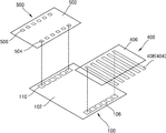
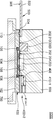
구체적으로, 광 집적 회로 패키지(1000)는 광 집적 회로 기판(102)을 포함하는 광 집적 회로(100, optical integrated circuit)를 포함할 수 있다. 광 집적 회로(100)는 인터포저(interposer)라고 명명할 수 있다. 광 집적 회로 기판(102)은 실리콘 반도체 기판으로 구성될 수 있다. 광 집적 회로 기판(102)은 III-V족 반도체 기판으로 구성될 수 있다. 광 집적 회로 기판(102)에는 광 도파로(104) 및 광 커플러(106)가 형성될 수 있다. Specifically, the optical
광 도파로(104) 및 광 커플러(106)는 도 1의 단면도와 같이 광 집적 회로 기판(102)의 내부에 형성된 것으로 도시하였으나, 광 도파로(104) 및 광 커플러(106)는 광 집적 회로 기판(102)의 표면 상에 형성될 수 있다. 광 커플러(106)는 수직형 광 커플러일 수 있다. 광 도파로(104)는 광(또는 광 신호)이 진행하는 통로일 수 있다. 광 커플러(106)는 광 집적 회로 기판(102)의 수평 방향으로 진행하는 광을 수직 방향으로 커플링할 수 있다. Although the
광 집적 회로 기판(102) 상에 전기 집적 회로 소자(200, electronic integrated circuit device, EICD)가 위치할 수 있다. 전기 집적 회로 소자(200)는 접착층(202)을 이용하여 광 집적 회로 기판(102)에 부착될 수 있다. 전기 집적 회로 소자(200)의 연결 패드(204)는 광 집적 회로 기판(102)의 일부분 상에 형성된 제1 배선 패드(108)에 전기적으로 연결될 수 있다.An electronic integrated circuit device (EICD) 200 may be located on the optical
광 집적 회로 기판(102) 상에는 전기 집적 회로 소자(200)와 떨어져서 적어도 하나의 광 소자(300, optical device, OD)가 설치될 수 있다. 광 소자(300)는 접착층(302)을 이용하여 광 집적 회로 기판(102)에 부착될 수 있다. 광 소자(300)는 전광 변환 소자, 광전 변환 소자 또는 광 변조 소자 등을 포함할 수 있다. 도 1의 광 소자(300)는 전광 변환 소자(310), 예컨대 레이저 다이오드 소자를 포함할 수 있다. 전광 변환 소자(310)에서 발생된 광(또는 광 신호)은 광 커플러(106)를 통하여 광 도파로(104)로 전송될 수 있다. At least one
광 집적 회로 기판(102)의 일측에 광 인터페이스(400, optical interface)가 설치될 수 있다. 광 인터페이스(400)는 접착층(402)을 이용하여 광 집적 회로 기판(102)에 접착될 수 있다. 광 인터페이스(400)는 광 집적 회로 기판(102)과 광학적으로 연결될 수 있다. 광 인터페이스(400)는 광 커플러(106)를 통해 광 도파로(104)와 광학적으로 연결될 수 있다. An
광 인터페이스(400)는 하나의 광 파이버(404)로 구성될 수 있다. 광 파이버(404)는 보호층(406)으로 보호될 수 있다. 광 인터페이스(400)는 후술하는 바와 같이 복수개의 광 파이버들을 포함하는 광 파이버 어레이일 수 있다. 광 파이버(404)는 화살표로 표시한 바와 같이 입출력 광의 경로를 변경하는 경사 단면부(408)를 포함할 수 있다. The
광 집적 회로 기판(102)의 타측에 전기 인터페이스(500, electrical interface)가 설치될 수 있다. 전기 인터페이스(500)는 광 집적 회로 기판(102)에 형성된 제2 배선 패드(110)에 전기적으로 연결될 수 있다. 전기 인터페이스(500)는 플렉서블 인쇄 회로 기판(502)으로 구성될 수 있다. 플렉서블 인쇄 회로 기판(502)의 일측에 형성된 제1 연결 패드(504)는 제2 배선 패드(110)와 전기적으로 연결될 수 있다. An
제1 배선 패드(108)와 제2 배선 패드(110)는 회로 배선 라인(미도시)을 통하여 서로 전기적으로 연결될 수도 있고, 그렇지 않을 수도 있다. 플렉서블 인쇄 회로 기판(502)의 타측에 형성된 제2 연결 패드(506)는 외부의 베이스 인쇄 회로 기판과 연결될 수 있다. 제2 연결 패드(506)는 제2 배선 패드(110)와 전기적으로 연결될 수 있다. 제2 연결 패드(506)를 통한 전기적 신호는 플렉서블 인쇄 회로 기판(502)을 통하여 제2 배선 패드(110)에 전달될 수 있다. The
필요에 따라서, 광 집적 회로 기판(102)의 하부에 광 집적 회로 기판(102)과 접촉하는 히트 싱크(700)가 설치될 수 있다. 히트 싱크(700)는 광 집적 회로(100)에서 발생되는 열을 외부로 방출하는 역할을 수행할 수 있다. If necessary, a
광 집적 회로 패키지(1000)는 광 집적 회로(100), 전기 집적 회로 소자(200), 광 소자(300), 광 인터페이스(400), 및 전기 인터페이스(500)를 밀봉하는 봉지 부재(600)를 포함할 수 있다. 일 실시예에서, 봉지 부재(600)의 내부는 공기층, 질소층 또는 진공층으로 채워져 있을 수 있다. 일 실시예에서, 봉지 부재(600)는 투명 물질층으로 채워져 있을 수 있다. 히트 싱크(700)가 설치될 경우, 봉지 부재(600)는 히트 싱크(700)의 양측에 접촉하면서 히트 싱크(700)를 밀봉할 수 있다. The optical
이상과 같이 광 집적 회로 패키지(1000)는 광 집적 회로 기판(102)을 포함하는 광 집적 회로(100). 광 집적 회로 기판(102) 상에 위치하는 전기 집적 회로 소자(200), 및 광 집적 회로 기판(102) 상에 형성된 광 인터페이스(400) 및 전기 인터페이스(500)를 포함할 수 있다. As described above, the optical
이에 따라, 광 집적 회로 패키지(1000)는 광 집적 회로 기판(102) 상에 다양한 광 소자들을 실장할 수 있고, 외부 기기와의 광학적 및 전기적인 연결을 용이하게 수행할 수 있음과 아울러 광 인터페이스(400)를 구비하여 전자 장치의 소형화 및 고속화의 요구에 부응할 수 있다. 또한, 광 집적 회로 패키지(1000)는 광 집적 회로 기판(102)과 광 인터페이스(400) 및 전기 인터페이스(500)간의 광 및 전기적 연결을 좋게 하여 신호 전송의 품질을 향상시킬 수 있다. Accordingly, the optical
도 2는 도 1의 광 집적 회로 패키지의 광 집적 회로와 광 인터페이스 및 전기 인터페이스와의 연결 관계를 도시한 사시도이다.2 is a perspective view showing a connection relationship between an optical integrated circuit of the optical integrated circuit package of FIG. 1 and an optical interface and an electrical interface.
구체적으로, 광 집적 회로(100)를 구성하는 광 집적 회로 기판(102)의 일측에 광 인터페이스(400)가 설치될 수 있다. 광 집적 회로 기판(102)에는 복수개의 광 커플러(106)들이 형성될 수 있다. 광 인터페이스(400)는 복수개의 광 파이버들(404)을 포함하는 광 파이버 어레이(408)일 수 있다. 광 파이버 어레이(408)는 보호층(406)으로 보호될 수 있다. Specifically, the
이에 따라, 광 파이버 어레이(408)는 광 커플러들(106)과 광학적으로 연결될 수 있다. 다시 말해, 광 파이버 어레이(408)와 광 커플러들(106)은 광(또는 광 신호)을 상호 전달할 수 있다. Accordingly, the
광 집적 회로 기판(102)의 타측에 전기 인터페이스(500)가 설치될 수 있다. 전기 인터페이스(500)는 플렉서블 인쇄 회로 기판으로 구성될 수 있다. 광 집적 회로 기판(102)의 타측에 복수개의 제2 배선 패드들(110)이 형성될 수 있다. An
플렉서블 인쇄 회로 기판(502)의 일측 및 타측에는 각각 제1 연결 패드들(504) 및 제2 연결 패드들(506)이 설치될 수 있다. 제1 연결 패드들(504)은 제2 배선 패드들(110)과 전기적으로 연결될 수 있다. 제2 연결 패드들(506)은 외부의 베이스 인쇄 회로 기판과 연결될 수 있다. 베이스 인쇄 회로 기판은 응용 모듈(또는 응용 기기)의 회로 기판일 수 있다. 제1 연결 패드들(504) 및 제2 연결 패드들(506)은 인터페이스 배선 라인(미도시)을 통하여 전기적으로 연결될 수 있다.
이에 따라, 전기 인터페이스(500)는 광 집적 회로 기판(102)과 전기적으로 연결될 수 있다. 다시 말해, 전기 인터페이스(500)의 제2 연결 패드(506)를 통한 전기적 신호는 플렉서블 인쇄 회로 기판(502)을 통하여 제2 배선 패드(110)에 전달될 수 있다.Accordingly, the
도 3은 도 1의 광 집적 회로 패키지의 광 소자 및 전기 집적 회로 소자간의 전기적 및 광학적 연결에 대한 일 실시예를 설명하기 위하여 도시한 평면도이다.3 is a plan view for explaining an electrical and optical connection between an optical element and an electric integrated circuit element of the optical integrated circuit package of FIG.
구체적으로, 앞서 설명한 바와 같이 광 집적 회로 패키지(1000)는 광 집적 회로(100), 전기 집적 회로 소자(200) 및 광 소자(300), 전기 인터페이스(500), 광 인터페이스(400) 및 히트 싱크(700)를 포함할 수 있다. Specifically, as described above, the optical
전기 인터페이스(500)의 인터페이스 배선 라인(503)을 통하여 전달되는 전기 신호는 회로 배선 라인(103)을 통하여 전기 집적 회로 소자(200) 및 광 소자(300)에 수신될 수 있다. 광 소자(300)가 전광 변환 소자, 예컨대 레이저 다이오드 소자인 경우 광 소자(300)에서 발생된 광 신호는 광 도파로(104)를 통하여 광 인터페이스(400)의 광 파이버 어레이(408) 또는 광 파이버(404)를 통하여 외부로 전달될 수 있다.An electric signal transmitted through the
한편, 외부에서 광 인터페이스(400)를 구성하는 광 파이버 어레이(408) 또는 광 파이버(404)를 통하여 수신되는 광 신호는 광 도파로(104)를 통하여 광 소자(300), 예컨대 광전 변환 소자로 수신될 수 있다. 광전 변환 소자는 포토 다이오드 소자일 수 있다. 광 소자(300)에서 변환된 전기 신호는 전기 집적 회로 소자(200)를 통하여 전기 인터페이스(500)의 인터페이스 배선 라인(503)을 통하여 외부로 전달될 수 있다. On the other hand, an optical signal received through the
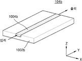
도 4 내지 도 6은 도 1의 광 집적 회로 패키지의 광 도파로의 다양한 실시예를 설명하기 위하여 도시한 평면도들이다. Figs. 4 to 6 are plan views illustrating various embodiments of the optical waveguide of the optical integrated circuit package of Fig. 1. Fig.
구체적으로, 도 1의 광 도파로(104)는 도 4 내지 도 6에서 광 도파로들(104a, 104b, 104c)을 포함할 수 있다. 도 4 내지 도 6에서, Y는 깊이 방향이고, X는 폭 방향일 수 있다. Specifically, the
도 4를 참조하면, 광 도파로(104a)는 하부 클래딩층(1002a) 및 하부 클래딩층(1002a) 상에 1차원 평면의 슬랩(slab)형으로 배치되는 코어층(1004a)을 포함할 수 있고, 공기층을 상부 클래딩층으로 이용할 수 있으나, 이에 한정되지 않는다. 이 경우, 깊이 방향(Z)으로만 굴절률 변화가 발생하므로, 광 도파로(104a)를 지나는 광 신호는 깊이 방향(Z)으로만 굴절된다. 도 4에서, 일측에서 입력된 광 신호는 타측으로 출력될 수 있다. 4, the
도 5를 참조하면, 광 도파로(104b)는 하부 클래딩층(1002b) 및 하부 클래딩층(1002b)에서 채널형으로 배치되는 코어층(1004b)을 포함할 수 있고, 공기층을 상부 클래딩층으로 이용할 수 있으나, 이에 한정되지 않는다. 이 경우, 굴절률의 변화는 채널의 깊이 방향(Z)과 폭 방향(X)으로 이루어진다. 도 5에서, 일측에서 입력된 광 신호는 타측으로 출력될 수 있다.5, the
도 6을 참조하면, 광 도파로(104c)는 하부 클래딩층(1002c) 및 하부 클래딩층(1002c)에서 분기되는(branching) 채널형으로 배치되는 코어층(1004c)을 포함할 수 있고, 공기층을 상부 클래딩층으로 이용할 수 있으나, 이에 한정되지 않는다. 도 6에서, 일측에서 입력된 광 신호는 타측으로 출력되며, 광 도파로(104c)는 입력된 광 신호를 두 개로 분기될 수 있다.Referring to FIG. 6, the
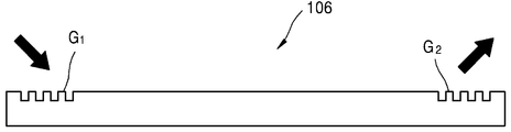
도 7은 도 1의 광 집적 회로 패키지의 광 커플러의 일 실시예를 설명하기 위하여 도시한 단면도이다. 7 is a cross-sectional view illustrating one embodiment of an optical coupler of the optical integrated circuit package of FIG.
구체적으로, 광 커플러(106)는 그레이팅 커플러일 수 있다. 광 커플러(106)는 광 도파로의 일단에 그레이팅, 즉, 격자(G1, G2)를 형성함으로써 구현할 수 있다. 광 커플러(106)는 광이 격자(G1, G2)를 만나면서 회절하는 특성을 이용하여, 광을 송수신할 수 있고, 격자(G1, G2)의 간격을 조절함으로써 광을 필터링할 수도 있다. Specifically, the
광 커플러(106)에 형성되는 그레이팅의 사이즈, 즉 그레이팅의 주기는 입사되는 광의 폭(w)과 파수 벡터(k-vector)에 의해 결정될 수 있다. 그에 따라, 광 커플러(106)에 적절한 그레이팅이 형성됨으로써, 해당 입사광이 높은 광 커플링 효율을 가지고 광 커플러(106)에 광 결합할 수 있다. The size of the grating formed on the
도 8은 도 7의 광 커플러를 통한 광 커플링 원리를 설명하기 위한 도면이다. 8 is a view for explaining the principle of optical coupling through the optical coupler of FIG.
구체적으로, 도 7의 광 커플러(106)를 이용한 광 커플링 조건을 아래에서 설명한다. 우선, 입사광이 높은 광 커플링 효율로 광 커플러(106)에 광 결합하기 위해서는 그 위상이 일치하여야 한다. 그러한 위상 매칭 조건은 아래의 수학식 1과 같이 나타난다.Specifically, the optical coupling condition using the
[수학식 1][Equation 1]
βν = β0 + ν2π/Λ? v =? 0 +? 2? /?
여기서, ν는 정수이고, Λ는 그레이팅의 주기를 나타내며, βν는 ν번째 모드의 위상을 나타내며, β0은 기본(fundamental) 모드의 위상을 나타낸다.Where v is an integer, [Lambda] represents the period of the grating, [beta] v represents the phase of the v-th mode, and [beta] represents the phase of the fundamental mode.
또한, 입사광이 도파로로 구속되기 위한 조건인 가이딩 조건(guiding condition)은 아래의 수학식 2와 같이 나타난다.The guiding condition, which is a condition for the incident light to be confined to the waveguide, is expressed by Equation (2) below.
[수학식 2]&Quot; (2) "
αm =κn3sinθm=(2π/λn3)sinθm? m =? n3sin? m = (2? /? n3) sin? m
여기서, m는 정수이고, λ는 m번째 모드 광의 파장을 나타내며, κ는 파수로서 파장의 역수이다. 또한, αm는 m번째 모드 광의 굴절율 조건 값이고, θm는 m번째 모드 광의 입사각도이다. 도 8에서, w는 입사된 광의 폭을 나타내고, n1은 하부 클래딩층의 굴절율을 나타내고, n2는 코어층의 굴절율을 나타내며, n3는 도파로 외부 또는 상부 클래딩층의 굴절율을 나타낸다. 입사광이 도파로에 가이딩되기 위해서는 κn3<αm<κn2의 관계를 만족해야 한다.Here, m is an integer,? Represents a wavelength of the m-th mode light, and? Is a reciprocal of a wavelength as a wave number. Further,? M is the refractive index condition value of the mth mode light, and? M is the incident angle of the mth mode light. 8, w denotes the width of the incident light, n1 denotes the refractive index of the lower cladding layer, n2 denotes the refractive index of the core layer, and n3 denotes the refractive index of the outer or upper cladding layer. In order for the incident light to be guided to the waveguide, the relation of κn3 <αm <κn2 must be satisfied.
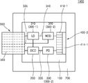
도 9는 본 발명의 기술적 사상의 일 실시예에 의한 광 집적 회로 패키지를 설명하기 위하여 도시한 평면도이다. 9 is a plan view illustrating an optical integrated circuit package according to an embodiment of the present invention.
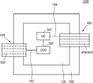
구체적으로, 도 9의 광 집적 회로 패키지(1100)는 도 1 내지 도 8의 광 집적 회로 패키지(1000)와 비교할 때 광 소자(300-1, 300-2)를 제외하고는 동일할 수 있다. 도 9의 광 집적 회로 패키지(1100)는 광 소자(300-1, 300-2) 및 전기 집적 회로 소자(200)간의 전기적 및 광학적 연결을 설명하기 위한 것이다. 도 9에서 도 1 내지 도 8과 동일한 참조번호는 동일한 부재를 나타내며, 편의상 중복되는 설명은 간단히 설명하거나 생략한다. Specifically, the optical
광 집적 회로 패키지(1100)는 광 집적 회로(100), 전기 집적 회로 소자(200), 광 소자(300-1, 300-2), 전기 인터페이스(500), 광 인터페이스(400) 및 히트 싱크(700)를 포함할 수 있다. 광 소자(300-1, 300-2)는 편의상 제1 광 소자(300-1)와 제2 광 소자(300-2)로 분류할 수 있다. The optical
제1 광 소자(300-1)는 광(또는 광 신호)을 발생시킬 수 있는 전광 변환 소자(LD), 예컨대 레이저 다이오드 소자일 수 있다. 제2 광 소자(300-2)는 광 신호 및 전기 신호를 프로세싱할 수 있는 광 변조기 소자(MOD, 320) 및 광전 변환 소자(PD, 330)를 포함할 수 있다. 광전 변환 소자(330)는 포토 다이오드 소자일 수 있다.The first optical device 300-1 may be an all-optical converter (LD), for example, a laser diode device capable of generating light (or optical signal). The second optical element 300-2 may include an optical modulator element (MOD) 320 and a photoelectric conversion element (PD) 330 capable of processing an optical signal and an electrical signal. The
전기 인터페이스(500)의 인터페이스 배선 라인(503)을 통하여 전달되는 전기 신호는 회로 배선 라인(335)을 통하여 전기 집적 회로 소자(200), 전광 변환 소자(310) 및 광 변조기 소자(320)로 전달될 수 있다. 전광 변환 소자(310)는 광 신호를 발생하여 광 변조기 소자(320)로 전달될 수 있다. The electric signal transmitted through the
광 변조기 소자(320)는 회로 배선 라인(335)을 통하여 전달되는 전기 신호에 따라 광 신호를 변조하여 광 도파로(104)를 통하여 광 인터페이스(400)로 전달할 수 있다. 변조된 광 신호는 광 인터페이스(400)의 광 파이버 어레이(408) 또는 광 파이버(404)를 통하여 외부로 전달될 수 있다. 필요에 따라서, 전기 집적 회로 소자(200)는 회로 배선 라인(335)을 통하여 전광 변환 소자(310)를 제어할 수 있다. The
한편, 외부에서 광 인터페이스(400)를 구성하는 광 파이버 어레이(408) 또는 광 파이버(404)를 통하여 수신되는 광 신호는 광 도파로(340)를 통하여 광전 변환 소자(330)로 수신될 수 있다. 광전 변환 소자(330)는 광 신호를 전기 신호로 변환하여 전기 집적 회로 소자(200) 및 회로 배선 라인(335)을 통하여 전기 인터페이스(500)로 전달할 수 있다. 전기 신호는 전기 인터페이스(500)의 인터페이스 배선 라인(503)을 통하여 외부로 전달될 수 있다. The optical signal received through the
이와 같이 광 집적 회로 패키지(1100)는 광 신호를 전송하거나 수신하는 광 트랜시버에 이용될 수 있다. 아울러서, 광 집적 회로 패키지(1100)는 복수개의 광 소자들(300-1, 300-2)을 포함하여 외부 기기와의 광학적 및 전기적인 연결을 용이하게 수행하고 광 인터페이스(400)를 구비하여 전자 장치의 소형화 및 고속화의 요구에 부응할 수 있다.Thus, the optical
도 10은 도 9의 광 집적 회로에 위치하는 광 소자들 및 전기 집적 회로 소자의 신호 흐름을 설명하기 위한 도면이다. FIG. 10 is a diagram for explaining signal flow of optical elements and electric integrated circuit elements located in the optical integrated circuit of FIG. 9; FIG.
구체적으로, 광 집적 회로(100) 내에 전기 집적 회로 소자(200, EICD), 전광 변환 소자(310, LD) 및 광 변조기 소자(MOD, 320)가 설치될 수 있다. 앞서 설명한 바와 같이 광 집적 회로 기판 상에 전기 집적 회로 소자(200, EICD), 전광 변환 소자(310, LD) 및 광 변조기 소자(MOD, 320)가 부착될 수 있다. Specifically, an electric
전기 집적 회로 소자(200)는 인가 받은 송신 데이터(MI)를 기초로 하여 송신 전기 신호들(VD)을 생성할 수 있다. 광 변조기 소자(320)는 송신된 전기 신호들(VD)에 따라 전광 변환 소자(310)로부터 수신된 광신호(LI)를 변조하여 변조된 광신호(LM)를 생성할 수 있다. 변조된 광신호(LM)는 외부 기기 또는 베이스 인쇄 회로 기판 등으로 전달될 수 있다.The electrical
도 11은 본 발명의 기술적 사상의 일 실시예에 의한 광 집적 회로 패키지의 단면도이다. 11 is a cross-sectional view of an optical integrated circuit package according to an embodiment of the present invention.
구체적으로, 광 집적 회로 패키지(1200)는 도 1 내지 도 8의 광 집적 회로 패키지(1000)와 비교할 때 광 인터페이스(400-1)를 제외하고는 동일할 수 있다. 도 11에서 도 1 내지 도 8과 동일한 참조번호는 동일한 부재를 나타내며, 편의상 중복되는 설명은 간단히 설명하거나 생략한다. Specifically, the optical
광 집적 회로 패키지(1200)는 광 집적 회로(100), 전기 집적 회로 소자(200), 광 소자(300), 전기 인터페이스(500), 광 인터페이스(400-1) 및 히트 싱크(700)를 포함할 수 있다.The optical
광 인터페이스(400-1)는 접착층(402)을 이용하여 광 집적 회로 기판(102)에 접착될 수 있다. 광 인터페이스(400-1)는 리셉터클 커넥터(414, receptacle connector), 렌즈(412) 및 정렬 소자(410)를 포함할 수 있다. 렌즈(412)는 선택적으로 설치될 수 있다. The optical interface 400-1 can be adhered to the optical
리셉터클 커넥터(414)는 정렬 소자(410) 상에 위치할 수 있다. 리셉터클 커넥터(414)는 광 신호를 전송할 수 있게 외부에서 플러그 커넥터(미도시)가 삽입될 수 있다. 정렬 소자(410)는 리셉터클 커넥터(414)를 통하여 입출입되는 광을 정렬할 수 있다. 정렬 소자(410)는 평면 광 도파로 소자일 수 있다. 정렬 소자(410)는 광 파이버의 코아층과 유사한 굴절률을 가지는 광 도파로를 포함할 수 있다. 정렬 소자(410)는 입출력 광의 경로를 변경하는 경사 단면부(408)를 포함할 수 있다. 정렬 소자(410)에는 후술하는 바와 같이 광다중화기 및 역다중화기가 설치될 수 있다. The
리셉터클 커넥터(414)를 통하여 전달되는 광(또는 광 신호)은 화살표로 도시한 바와 같이 렌즈(412) 및 정렬 소자(410)를 통하여 광 커플러(106)에 전달될 수 있다. 이에 따라, 광 인터페이스(400-1)는 광 커플러(106)를 통해 광 도파로(104)와 광학적으로 연결될 수 있다. 광 인터페이스(400-1)는 광 집적 회로 기판(102)과 광학적으로 연결될 수 있다. The light (or optical signal) transmitted through the
도 12는 본 발명의 기술적 사상의 일 실시예에 의한 광 집적 회로 패키지의 단면도이다. 12 is a cross-sectional view of an optical integrated circuit package according to an embodiment of the technical idea of the present invention.
구체적으로, 광 집적 회로 패키지(1300)는 도 1 내지 도 8의 광 집적 회로 패키지(1000)와 비교할 때 광 인터페이스(400-2)를 제외하고는 동일할 수 있다. 도 12에서 도 1 내지 도 8과 동일한 참조번호는 동일한 부재를 나타내며, 편의상 중복되는 설명은 간단히 설명하거나 생략한다. Specifically, the optical
광 집적 회로 패키지(1300)는 광 집적 회로(100), 전기 집적 회로 소자(200), 광 소자(300), 전기 인터페이스(500), 광 인터페이스(400-2) 및 히트 싱크(700)를 포함할 수 있다.The optical
광 인터페이스(400-2)는 접착층(402)을 이용하여 광 집적 회로 기판(102)에 접착될 수 있다. 광 인터페이스(400-1)는 리셉터클 커넥터(414-1, receptacle connector), 및 정렬 소자(410-1)를 포함할 수 있다. The optical interface 400-2 can be adhered to the optical
리셉터클 커넥터(414-1)는 정렬 소자(410-1)의 일측에 위치할 수 있다. 리셉터클 커넥터(414-1)를 도 11과 같이 정렬 소자(410) 상에 위치하지 않을 경우 패키지 높이를 낮출 수 있고 광 정렬을 용이하게 할 수 있다. The receptacle connector 414-1 may be located at one side of the alignment element 410-1. When the receptacle connector 414-1 is not positioned on the
리셉터클 커넥터(414-1)는 광 신호를 전송할 수 있게 외부에서 플러그 커넥터가 삽입될 수 있다. 정렬 소자(410-1)는 리셉터클 커넥터(414)를 통하여 입출입되는 광을 정렬할 수 있다. 정렬 소자(410-1)는 평면 광 도파로 소자일 수 있다. 정렬 소자(410-1)는 입출력 광의 경로를 변경하는 경사 단면부(408)를 포함할 수 있다.The receptacle connector 414-1 can be inserted with a plug connector from the outside so as to transmit an optical signal. The alignment element 410-1 can align the light input / output through the
리셉터클 커넥터(414-1)를 통하여 전달되는 광(또는 광 신호)은 화살표로 도시한 바와 같이 정렬 소자(410-1)를 통하여 광 커플러(106)에 전달될 수 있다. 이에 따라, 광 인터페이스(400-2)는 광 커플러(106)를 통해 광 도파로(104)와 광학적으로 연결될 수 있다. 광 인터페이스(400-2)는 광 집적 회로 기판(102)과 광학적으로 연결될 수 있다.The light (or optical signal) transmitted through the receptacle connector 414-1 can be transmitted to the
도 13은 도 11 및 도 12의 정렬 소자의 일 예를 도시한 사시도이다. 13 is a perspective view showing an example of the alignment element of Figs. 11 and 12. Fig.
구체적으로, 정렬 소자(410, 410-1)는 앞서 설명한 바와 같이 평면 광 도파로 소자로 구성할 수 있다. 정렬 소자(410, 410-1)는 하부 클래딩층(431), 복수의 정렬 광 도파로(433), 상부 클래딩층(435), 리드(437, lid)를 포함할 수 있다. 정렬 소자(410, 410-1)는 실리콘 질화물, 실리콘 산화물과 같이 1300nm 내지 1600nm의 파장 대역에서 투명한 물질로 구성될 수 있다. 정렬 소자(410, 410-1)의 광 도파로는 광 파이버의 코아층과 유사한 굴절률을 가질 수 있다.Specifically, the
정렬 소자(410, 410-1)는 정렬 칩이라고 명명할 수 있다. 정렬 광 도파로(433)는 하부 클래딩층(431) 상에 구현될 수 있다. 리드(437)는 필요에 따라 형성하거나 형성하지 않을 수 있다. The
정렬 소자(410) 상에는 도 11에 도시한 바와 같이 리셉터클 커넥터(414)가 위치할 수 있다. 정렬 소자(410-1)의 일측에는 도 12에 도시한 바와 같이 리셉터클 커넥터(414-1)가 위치할 수 있다. The
앞서 설명한 바와 같이 리셉터클 커넥터(414-1)를 통하여 전달되는 광 신호는 정렬 광 도파로(435)를 통하여 광 집적 회로 기판에 형성된 광 도파로로 전달 될 수 있다. As described above, the optical signal transmitted through the receptacle connector 414-1 can be transmitted through the alignment
도 14는 본 발명의 기술적 사상의 일 실시예에 의한 광 집적 회로 패키지를 설명하기 위하여 도시한 평면도이다. 14 is a plan view for explaining an optical integrated circuit package according to an embodiment of the technical idea of the present invention.
구체적으로, 광 집적 회로 패키지(1400)는 도 9의 광 집적 회로 패키지(1100)와 비교할 때 광 인터페이스(400-2)를 제외하고는 동일할 수 있다. 광 집적 회로 패키지(1400)는 광 소자(300-1, 300-2) 및 전기 집적 회로 소자(200)간의 전기적 및 광학적 연결을 설명하기 위한 것이다. Specifically, the optical
광 집적 회로 패키지(1400)는 도 13의 광 인터페이스(400-2)를 이용한 광 연결을 설명하기 위한 것이다. 도 14에서 도 9와 동일한 참조번호는 동일한 부재를 나타내며, 편의상 중복되는 설명은 간단히 설명하거나 생략한다. The optical
광 집적 회로 패키지(1400)는 광 집적 회로(100), 전기 집적 회로 소자(200), 광 소자(300-1, 300-2), 전기 인터페이스(500), 광 인터페이스(400-2) 및 히트 싱크(700)를 포함할 수 있다. 광 소자(300-1, 300-2)는 편의상 제1 광 소자(300-1)와 제2 광 소자(300-2)로 분류할 수 있다. The optical
제1 광 소자(300-1)는 광(또는 광 신호)을 발생시킬 수 있는 전광 변환 소자(LD), 예컨대 레이저 다이오드 소자일 수 있다. 제2 광 소자(300-2)는 광 신호 및 전기 신호를 프로세싱할 수 있는 광 변조기 소자(MOD, 320) 및 광전 변환 소자(PD, 330)를 포함할 수 있다. 광전 변환 소자(330)는 포토 다이오드 소자일 수 있다. The first optical device 300-1 may be an all-optical converter (LD), for example, a laser diode device capable of generating light (or optical signal). The second optical element 300-2 may include an optical modulator element (MOD) 320 and a photoelectric conversion element (PD) 330 capable of processing an optical signal and an electrical signal. The
전기 인터페이스(500)의 인터페이스 배선 라인(503)을 통하여 전달되는 전기 신호는 회로 배선 라인(335)를 통하여 전기 집적 회로 소자(200), 전광 변환 소자(310) 및 광 변조기 소자(320)로 전달될 수 있다. 전광 변환 소자(310)는 광 신호를 발생하여 광 변조기 소자(320)로 전달될 수 있다. The electric signal transmitted through the
광 변조기 소자(320)는 회로 배선 라인(335)을 통하여 전달되는 전기 신호에 따라 광 신호를 변조하여 광 도파로(104)를 통하여 광 인터페이스(400-2)로 전달할 수 있다. 변조된 광 신호는 광 인터페이스(400-2)의 정렬 소자(410-1) 및 리셉터클 커넥터(414-1)를 통하여 외부로 전달될 수 있다. 필요에 따라서, 전기 집적 회로 소자(200)는 회로 배선 라인(335)을 통하여 전광 변환 소자(310)를 제어할 수 있다. The
한편, 외부에서 광 인터페이스(400)를 구성하는 리셉터클 커넥터(414-1) 및 정렬 소자(410-1)를 통하여 수신되는 광 신호는 광 도파로(340)를 통하여 광전 변환 소자(330)로 수신될 수 있다. 광전 변환 소자(330)는 광 신호를 전기 신호로 변환하여 전기 집적 회로 소자(200) 및 회로 배선 라인(335)을 통하여 전기 인터페이스(500)로 전달할 수 있다. 전기 신호는 전기 인터페이스(500)의 인터페이스 배선 라인(503)을 통하여 외부로 전달될 수 있다. The optical signal received through the receptacle connector 414-1 and alignment element 410-1 constituting the
도 15는 본 발명의 기술적 사상의 일 실시예에 의한 광 집적 회로 패키지를 설명하기 위하여 도시한 단면도이다. 15 is a cross-sectional view illustrating an optical integrated circuit package according to an embodiment of the present invention.
구체적으로, 광 집적 회로 패키지(1500)는 도 1의 광 집적 회로 패키지(1000)와 비교할 때 광 소자(310-1, 300)를 제외하고는 동일할 수 있다. 도 15에서 도 1과 동일한 참조번호는 동일한 부재를 나타내며, 편의상 중복되는 설명은 간단히 설명하거나 생략한다. Specifically, the optical
광 집적 회로 패키지(1500)는 광 집적 회로(100), 전기 집적 회로 소자(200), 광 소자(310-1, 300), 전기 인터페이스(500), 광 인터페이스(400) 및 히트 싱크(700)를 포함할 수 있다. The optical
광 집적 회로 기판(102)의 내부에 적어도 하나의 광 소자(300, optical device, OD)가 설치될 수 있다. 광 소자(310-1, 300)는 전광 변환 소자(310), 예컨대 레이저 다이오드 소자를 포함할 수 있다. 전광 변환 소자(310-1)에서 발생된 광(또는 광 신호)은 광 커플러(106)를 통하여 광 도파로(104)로 전송될 수 있다. At least one optical device (OD) 300 may be installed in the optical
이와 같이 광 소자(310-1, 300)를 광 집적 회로 기판(102) 내에 형성할 경우, 광 도파로(104)와 광 소자(310-1, 300)와의 광 정렬을 용이하게 할 수 있고, 광 집적 회로 기판(102) 상에 광 소자 형성 영역이나 전기 집적 회로 소자 형성 영역을 확보할 수 있다.When the optical elements 310-1 and 300 are formed in the optical
도 16은 본 발명의 기술적 사상의 일 실시예에 의한 광 집적 회로 패키지를 설명하기 위하여 도시한 단면도이다. 16 is a cross-sectional view illustrating an optical integrated circuit package according to an embodiment of the present invention.
구체적으로, 광 집적 회로 패키지(1600)는 도 1의 광 집적 회로 패키지(1000)와 비교할 때 베이스 인쇄 회로 기판(710)을 더 포함하는 것을 제외하고는 동일할 수 있다. 도 16에서 도 1과 동일한 참조번호는 동일한 부재를 나타내며, 편의상 중복되는 설명은 간단히 설명하거나 생략한다. Specifically, the optical
광 집적 회로 패키지(1600)는 베이스 인쇄 회로 기판(710)을 더 포함할 수 있다. 베이스 인쇄 회로 기판(710)은 응용 모듈(또는 응용 기기)의 회로 기판일 수 있다. 광 집적 회로(100)는 베이스 인쇄 회로 기판(710) 내에 위치할 수 있다. 전기 인터페이스(500)의 제2 연결 패드(506)는 베이스 인쇄 회로 기판(710)의 배선 패드(720)에 전기적으로 연결될 수 있다. 광 인터페이스(400)는 베이스 인쇄 회로 기판(700) 상에 위치할 수 있다. The optical
이와 같이 광 집적 회로 패키지(1600)는 베이스 인쇄 회로 기판(710)에 실장할 수 있고, 베이스 회로 기판(710) 상에는 다양한 광 소자 및 전기 소자 등을 탑재하여 모듈화할 수 있다. Thus, the optical
도 17은 본 발명의 기술적 사상에 의한 일 실시예에 따른 광 집적 회로 패키지를 포함하는 광 집적 회로 시스템을 설명하기 위한 도면이다. 17 is a view for explaining an optical integrated circuit system including an optical integrated circuit package according to an embodiment of the present invention.
구체적으로, 도 15는 도 11 내지 도 14의 광 집적 회로 패키지(1200, 1300, 1400)를 포함하는 광 집적 회로 시스템(1700)을 설명하기 위하여 제공될 수 있다. 광 집적 회로 시스템(1700)은 복수의 전기 집적 회로 소자(EICD, 200_1 내지 200_n), 복수의 광 변조기 소자들(MOD, 320_1 내지 320_n), 복수의 광전 변환 소자들(PD. 330_1 내지 330_n), 정렬 소자(410, 410-1), 및 리셉터클 커넥터들(414, 414-1)을 포함할 수 있다. Specifically, FIG. 15 may be provided to illustrate an optical
정렬 소자(410, 410-1)는 광신호 다중화기(461, MUX), 및 광신호 역다중화기(464, DEMUX)를 포함할 수 있다. 광 집적 회로 시스템(1700)에서 편의상 전광 변환 소자는 도시하지 않는다. The
복수의 광 변조기 소자들(MOD, 320_1 내지 320_n)은 복수의 전기 집적 회로 소자(EICD, 200_1 내지 200_n)로부터 입력 받은 송신 전기 신호들(MI_1 내지 MI_n)을 각각 기초로 하여 변조된 송신 광신호들(LT_1 내지 LT_n)을 각각 생성할 수 있다. 이때, 변조된 송신 광신호들(LT_1 내지 LT_n) 각각은 서로 다른 파장을 가지는 광신호일 수 있다. The plurality of optical modulator elements MOD_3_1_1 to 320_n are connected to transmission optical signals modulated based on the transmission electrical signals MI_1 to MI_n received from the plurality of electrical integrated circuit elements (EICD, 200_1 to 200_n) (LT_1 to LT_n), respectively. At this time, each of the modulated transmission optical signals LT_1 to LT_n may be an optical signal having different wavelengths.
정렬 소자(410, 410-1)에 포함된 광신호 다중화기(461, MUX)는 변조된 송신 광신호들(LT_1 내지 LT_n)을 이용하여 다중화된 광신호를 생성하고, 리셉터클 커넥터들(414, 414-1)을 통하여 다중화된 광신호를 외부 장치 또는 베이스 인쇄 회로 기판으로 송신할 수 있다. The
외부 장치로부터 리셉터클 커넥터들(414, 414-1)을 통하여 송신된 다중화된 광신호는 정렬 소자(410, 410-1)에 포함된 광신호 역다중화기(464, DEMUX)에 제공될 수 있다. 광신호 역다중화기(464)는 리셉터클 커넥터들(414, 414-1)로부터 입력 받은 다중화된 광신호를 변조된 수신 광신호들(LR_1 내지 LR_n)로 역 다중화할 수 있다. 이때, 변조된 수신 광신호들(LR_1 내지 LR_n) 각각은 서로 다른 파장을 가지는 광신호일 수 있다. The multiplexed optical signal transmitted from the external device via the
복수의 광전 변환 소자들(PD. 330_1 내지 330_n)은 변조된 수신 광신호들(LR_1 내지 LR_n)을 각각 기초로 하여 변조된 수신 전기 신호들(MO_1 내지 MO_n)을 각각 생성하여 복수의 전기 집적 회로 소자(EICD, 200_1 내지 200_n)로 제공할 수 있다.The plurality of photoelectric conversion elements PD 330_1 to 330_n respectively generate the modulated received electrical signals MO_1 to MO_n on the basis of the modulated optical signals LR_1 to LR_n, Device (EICD, 200_1 to 200_n).
도 18은 본 발명의 기술적 사상에 의한 일 실시예에 따른 광 집적 회로 패키지를 포함하는 광 집적 회로 시스템을 설명하기 위한 도면이다.18 is a view for explaining an optical integrated circuit system including an optical integrated circuit package according to an embodiment of the present invention.
구체적으로, 광 집적 회로 시스템(2000)은 접속 시스템(2013)을 경유하여 적어도 하나의 메모리 모듈(2008)과 통신할 수 있는 중앙처리장치(CPU, 2002)를 포함한다. 메모리 모듈(2008)은 예컨대, 듀얼 인라인 메모리 모듈(DIMM)일 수 있다. DIMM은 DRAM 모듈일 수 있다. 메모리 모듈(2008)은 복수개의 개별 메모리 회로(2020), 예컨대 DRAM 메모리 회로를 포함할 수 있다. Specifically, the optical
본 실시예에서, CPU(2002) 및 메모리 모듈(2008)은 전기 신호를 발생하거나 처리한다. 접속 시스템(2013)은 CPU(2002) 및 메모리 모듈(2008) 사이에 광신호를 전달하는 광통신 채널(2012), 예컨대 광 파이버를 포함할 수 있다. In this embodiment, the
CPU(2002) 및 메모리 모듈(2008)은 전기 신호를 이용하기 때문에, 광통신 채널 상에서 전달을 위해 CPU(2002) 및 메모리 모듈 (2008)의 전기 신호를 광신호로 변환하는 전광 변환이 요구된다. 또한, 광전 변환은 광통신 채널(2012) 상의 광신호를 CPU(2002) 및 메모리 모듈(2008)에 처리를 위한 전기 신호로 변환하는 것이 요구된다. Since the
접속 시스템(2013)은 광통신 채널(2012)의 양측에 본 발명의 기술적 사상의 일 실시예에 의한 광 집적 회로 패키지(2004, 2006)를 포함할 수 있다. 광 통신 채널(2012)은 본 발명의 기술적 사상의 광 집적 회로 패키지의 광 인터페이스일 수 있다. The
CPU(2002)는 전기 버스(2010)를 경유하여 광 집적 회로 패키지(2004)와 전기 신호를 송수신할 수 있다. 메모리 모듈(2008)은 전기 버스(2014)를 경유하여 광 집적 회로 패키지(2006)와 전기 신호를 송수신한다. 광 집적 회로 패키지(2004, 2006)들은 서로 광 신호를 송수신할 수 있다. 전기 버스(2010, 2014)는 본 발명의 기술적 사상의 광 집적 회로 패키지의 전기 인터페이스일 수 있다. The
광 집적 회로 패키지(2004)는 광전 변환 소자(2016) 및 전광 변환 소자(2017)를 포함할 수 있다. 광 집적 회로 패키지(2006)는 광전 변환 소자(2018) 및 전광 변환 소자(2019)를 포함할 수 있다. 전광 변환 소자(2017, 2019)는 광통신 채널(2012), 예컨대, 광 파이버쪽으로 광 신호를 송신할 수 있다. 광전 변환 소자(2016, 2018)는 광통신 채널(2012)로부터 광신호를 수신할 수 있다. The optical
도 19는 본 발명의 기술적 사상에 의한 일 실시예에 따른 광 집적 회로 패키지를 포함하는 광 집적 회로 시스템을 설명하기 위한 도면이다.19 is a view for explaining an optical integrated circuit system including an optical integrated circuit package according to an embodiment of the present invention.
구체적으로, 광 집적 회로 시스템(2050)은 접속 시스템(2063)을 통해 적어도 하나의 메모리 모듈(2058)과 통신할 수 있는 CPU(2052)를 포함한다. 메모리 모듈(2058)은 예컨대 듀얼 인라인 메모리 모듈(DIMM)일 수 있다. 메모리 모듈 (2058)은 예컨대 DRAM 모듈일 수 있다. 메모리 모듈 (2058)은 복수개의 개별 메모리 회로(2070), 예컨대 DRAM 메모리 회로를 포함할 수 있다. Specifically, the optical
본 실시예에서, CPU(2052) 및 메모리 모듈(2058)은 전기 신호 및 광신호를 발생하거나 처리할 수 있다. 도 19의 실시예는 본 발명의 기술적 사상의 광 집적 회로 패키지(2076, 2082)가 CPU(2052) 및 메모리 모듈(2058)에 구현되어 있다. In this embodiment, the
CPU(2052)는 광 집적 회로 패키지(2076)를 포함하고, 메모리 모듈(2058)은 광 집적 회로 패키지(2082)를 포함할 수 있다. 광 집적 회로 패키지(2076)는 광전 변환 소자(2077) 및 전광 변환 소자(2079)를 포함할 수 있다. 광 집적 회로 패키지(2082)는 광전 변환 소자(2083) 및 전광 변환 소자(2081)를 포함할 수 있다.The
CPU(2052)에서 전기 회로(2078)을 포함하고, 전기 버스(2080)를 경유하여 광 집적 회로 패키지(2076)쪽으로 및 광 집적 회로 패키지(2076)로부터의 전기 신호와 통신한다. 메모리 모듈(2058)에서 메모리 회로(2070)를 포함하고, 전기 버스(2084)를 통해 광 집적 회로 패키지(2082)쪽으로 및 광 집적 회로 패키지(2082)로부터의 전기 신호와 통신한다. 전기 버스(2080, 2084)는 본 발명의 기술적 사상의 광 집적 회로 패키지의 전기 인터페이스일 수 있다.The
접속 시스템(2063)은 광통신 채널(2062)을 포함하고, 광통신 채널(2062)은 CPU(2052) 및 메모리 모듈(2058) 사이의 광신호를 전달한다. 광통신 채널(2062)은 예컨대 광파이버일 수 있다. 광 통신 채널(2062)은 본 발명의 기술적 사상의 광 집적 회로 패키지의 광 인터페이스일 수 있다. The
CPU(2052)는 광 커넥터(2072)를 포함할 수 있다. 광 커넥터는 본 발명의 기술적 사상의 리셉터클 커넥터일 수 있다. 광 커넥터(2072)를 통해 광 집적 회로 패키지(2076)로부터 광통신 채널(2062)쪽으로 광신호가 전송된다. 또한, 광 커넥터(2072)를 통해 광통신 채널(2062)쪽에서 광 집적 회로 패키지(2076)로 광신호가 전송된다. The
메모리 모듈(2058)은 광 커넥터(2074)를 포함한다. 광 커넥터(2074)를 통해 광 집적 회로 패키지(2082)로부터 광통신 채널(2062)쪽으로 광신호가 전송된다. 또한, 광 커넥터(2074)를 통해 광통신 채널(2062)쪽에서 광 집적 회로 패키지(2082)로 광신호가 전송될 수 있다. The
도 20은 본 발명의 기술적 사상에 의한 일 실시예에 따른 광 집적 회로 패키지를 포함하는 광 집적 회로 시스템을 설명하기 위한 도면이다.20 is a view for explaining an optical integrated circuit system including an optical integrated circuit package according to an embodiment of the present invention.
구체적으로, 광 집적 회로 시스템(2100)은 접속 시스템(2113)을 통해 적어도 하나의 메모리 모듈(2108)과 통신할 수 있는 CPU(2102)를 포함할 수 있다. 메모리 모듈(2108)은 예컨대 듀얼 인라인 메모리 모듈(DIMM)일 수 있다. 메모리 모듈(2108)은 DRAM 모듈일 수 있다. 메모리 모듈(2108)은 복수개의 개별 메모리 회로(2120), 예컨대 DRAM 메모리 소자를 포함할 수 있다. Specifically, the optical
본 실시예에서, CPU(2102) 및 메모리 모듈(2108)은 전기 신호 및 광신호를 발생하거나 처리할 수 있다. 도 20의 실시예는 CPU(2102) 및 개별 메모리 소자(2120)에 본 발명의 광 집적 회로 패키지(2115, 2121)가 구현되어 있다. In this embodiment, the
광 집적 회로 패키지(2115)는 광전 변환 소자(2116) 및 전광 변환 소자(2117)를 포함할 수 있다. 광 집적 회로 패키지(2121)는 광전 변환 소자(2123) 및 전광 변환 소자(2126)를 포함할 수 있다.The optical
CPU(2102)는 광 집적 회로 패키지(2115)를 포함하고, 메모리 회로(2120) 각각은 광 집적 회로 패키지(2121)를 포함할 수 있다. CPU(2102)는 전기 회로(2128)를 포함하고, 전기 버스(2130)를 경유하여 광 집적 회로 패키지(2115)쪽으로 및 광 집적 회로 패키지(2115)로부터의 전기 신호와 통신한다.The
각각 메모리 회로(2120)는 전기 회로(2127)를 포함하고, 전기 버스(2125)를 통해 광 집적 회로 패키지(2121)쪽으로 및 광 집적 회로 패키지(2121)로부터의 전기 신호와 통신한다. 전기 버스(2125, 2130)는 본 발명의 기술적 사상의 광 집적 회로 패키지의 전기 인터페이스일 수 있다.Each
배선 시스템(2113)은 광 통신 채널(2112)을 포함하고, 광 통신 채널(2112)은 CPU(2102) 및 메모리 모듈(2108) 사이의 광신호를 전달한다. 광 통신 채널(2112)는 예컨대 광파이버일 수 있다. 광 통신 채널(2112)은 본 발명의 기술적 사상의 광 집적 회로 패키지의 광 인터페이스일 수 있다. CPU(2102)는 광 커넥터(2122)를 포함한다. The
광 커넥터(2122)를 통해 광 집적 회로 패키지(2115)로부터 광통신 채널(2112)쪽으로 광신호가 전송된다. 또한, 광 커넥터(2122)를 통해 광통신 채널(2112)쪽에서 광 집적 회로 패키지(21115)로 광신호가 전송된다. The optical signal is transmitted from the optical
메모리 모듈(2108)은 광 커넥터(2124)를 포함한다. 광 커넥터(2124) 및 광 버스(2134)를 통해 광 집적 회로 패키지(2121)로부터 광통신 채널(2112)쪽으로 광신호가 전송된다. 또한, 광 커넥터(2124)를 통해 광통신 채널(2112)쪽에서 광 집적 회로 패키지(2121)로 광신호가 전송된다.The
도 21은 본 발명의 기술적 사상에 의한 일 실시예에 따른 광 집적 회로 패키지를 포함하는 컴퓨터 시스템을 설명하기 위한 블록도이다.21 is a block diagram illustrating a computer system including an optical integrated circuit package according to an embodiment of the present invention.
구체적으로, 컴퓨터 시스템(2200)은 어떠한 종류의 신호 처리 시스템, 디스플레이(display) 시스템, 통신(communication) 시스템 또는 신호가 광적으로 전송될 수 있는 다른 시스템을 포함할 수 있다. In particular,
컴퓨터 시스템(2200)은 광 버스(2250)에 의해 다른 요소와 통신할 수 있는 프로세서(2210)를 포함할 수 있다. 프로세서(2210)는 본 발명의 기술적 사상에 의한 광 집적 회로 패키지(2202)를 포함할 수 있다.
반도체 메모리 장치(2220)는 광 버스(2250)에 커플링되어 있다. 반도체 메모리 장치(2220)는 본 발명 사상에 의한 광 집적 회로 패키지를 포함할 수 있다. 이에 따라, 반도체 메모리 장치(2220)는 광 버스(2250)에 의해 다른 요소와 통신할 수 있다. 전원 공급 장치(2240)는 광 버스(2250)에 의해 다른 요소와 통신할 수 있다. 사용자 인터페이스(2230)는 사용자쪽으로 및 그로부터 입력/출력을 제공할 수 있다.
이상 본 발명을 도면에 도시된 실시예를 참고로 설명하였으나 이는 예시적인 것에 불과하며, 본 기술 분야의 통상의 지식을 가진 자라면 이로부터 다양한 변형, 치환 및 균등한 타 실시예가 가능하다는 점을 이해할 것이다. 이상에서 기술한 실시예들은 모든 면에서 예시적인 것이며 한정적이 아닌 것으로 이해하여야 한다. 본 발명의 진정한 기술적 보호 범위는 첨부된 특허청구범위의 기술적 사상에 의해 정해져야 할 것이다.While the present invention has been particularly shown and described with reference to exemplary embodiments thereof, it is to be understood that the invention is not limited to the disclosed embodiments, but, on the contrary, is intended to cover various modifications and equivalent arrangements included within the spirit and scope of the appended claims. will be. It is to be understood that the above-described embodiments are illustrative and non-restrictive in every respect. The true scope of the present invention should be determined by the technical idea of the appended claims.
1000: 광 집적 회로 패키지, 102: 광 집적 회로 기판, 100: 광 집적 회로, 104: 광 도파로, 106: 광 커플러, 200: 전기 집적 회로 소자, 300: 광 소자, 400: 광 인터페이스, 404: 광 파이버, 500: 전기 인터페이스, 502: 플렉서블 인쇄 회로 기판, 600: 봉지 부재, 700: 히트 싱크, The present invention relates to an optical integrated circuit package and a method of manufacturing the same, and more particularly, to an optical integrated circuit package, Fiber, 500: electrical interface, 502: flexible printed circuit board, 600: sealing member, 700: heat sink,
Claims (20)
상기 광 집적 회로 기판 상에 위치하는 전기 집적 회로 소자;
상기 전기 집적 회로 소자와 떨어져서 상기 광 집적 회로 기판 상에 위치하는 적어도 하나의 광 소자;
상기 광 집적 회로 기판의 일측에 위치하는 광 인터페이스;
상기 광 집적 회로 기판의 타측에 위치하는 전기 인터페이스; 및
상기 광 집적 회로, 상기 전기 집적 회로 소자, 상기 광 소자, 상기 광 인터페이스, 및 상기 전기 인터페이스를 밀봉하는 봉지 부재를 포함하는 것을 특징으로 하는 광 집적 회로 패키지. An optical integrated circuit including an optical integrated circuit board;
An electric integrated circuit device located on the optical integrated circuit board;
At least one optical element located on the optical integrated circuit board away from the electric integrated circuit element;
An optical interface located at one side of the optical integrated circuit board;
An electrical interface located on the other side of the optical integrated circuit board; And
And an encapsulating member sealing the optical integrated circuit, the electric integrated circuit element, the optical element, the optical interface, and the electrical interface.
상기 광 집적 회로 기판 상에 위치하여 상기 광 집적 회로 기판의 배선 라인과 전기적으로 연결된 전기 집적 회로 소자;
상기 광 집적 회로에서 광 신호 및 전기 신호를 프로세싱하는 적어도 하나의 광 소자;
상기 광 집적 회로 기판의 일측에 위치하고 상기 광 집적 회로 및 광 소자와 광학적으로 연결된 광 인터페이스;
상기 광 집적 회로 기판의 타측에 위치하고 상기 전기 집적 회로 소자 및 광 소자와 전기적으로 연결된 전기 인터페이스; 및
상기 광 집적 회로, 상기 전기 집적 회로 소자, 상기 광 소자, 상기 광 인터페이스, 및 상기 전기 인터페이스를 밀봉하는 봉지 부재를 포함하는 것을 특징으로 하는 광 집적 회로 패키지. An optical integrated circuit including an optical integrated circuit board;
An electric integrated circuit device located on the optical integrated circuit board and electrically connected to a wiring line of the optical integrated circuit board;
At least one optical element for processing an optical signal and an electrical signal in the optical integrated circuit;
An optical interface located at one side of the optical integrated circuit board and optically connected to the optical integrated circuit and the optical element;
An electrical interface located on the other side of the optical integrated circuit board and electrically connected to the electrical integrated circuit element and the optical element; And
And an encapsulating member sealing the optical integrated circuit, the electric integrated circuit element, the optical element, the optical interface, and the electrical interface.
상기 광 집적 회로 기판 상에 위치하여 상기 광 집적 회로 기판의 배선 라인과 전기적으로 연결된 전기 집적 회로 소자;
상기 광 집적 회로 기판의 내부에 집적되어 광 신호를 발생시킬 수 있는 제1 광 소자;
상기 광 집적 회로 기판 상에 위치하여 광 신호 및 전기 신호를 프로세싱하는 제2 광 소자;
상기 광 집적 회로 기판의 일측에 위치하고 상기 광 집적 회로, 제1 광 소자 및 제2 광 소자와 광학적으로 연결된 광 인터페이스;
상기 광 집적 회로 기판의 타측에 위치하고 상기 전기 집적 회로, 제1 광 소자, 및 제2 광 소자와 전기적으로 연결된 전기 인터페이스; 및
상기 광 집적 회로, 상기 전기 집적 회로 소자, 상기 제1 광 소자, 상기 제2 광 소자, 상기 광 인터페이스, 및 상기 전기 인터페이스를 밀봉하는 봉지 부재를 포함하여 이루어지는 것을 특징으로 하는 광 집적 회로 패키지. An optical integrated circuit including an optical integrated circuit board;
An electric integrated circuit device located on the optical integrated circuit board and electrically connected to a wiring line of the optical integrated circuit board;
A first optical element integrated in the optical integrated circuit board to generate an optical signal;
A second optical device positioned on the optical integrated circuit board to process an optical signal and an electrical signal;
An optical interface located at one side of the optical integrated circuit board and optically connected to the optical integrated circuit, the first optical device and the second optical device;
An electrical interface located on the other side of the optical integrated circuit board and electrically connected to the electrical integrated circuit, the first optical device, and the second optical device; And
And an encapsulation member sealing the optical integrated circuit, the electric integrated circuit element, the first optical element, the second optical element, the optical interface, and the electrical interface.
Priority Applications (2)
| Application Number | Priority Date | Filing Date | Title |
|---|---|---|---|
| US15/257,038 US9939596B2 (en) | 2015-10-29 | 2016-09-06 | Optical integrated circuit package |
| CN201610971029.3A CN106959488A (en) | 2015-10-29 | 2016-10-28 | Optical integrated circuit is encapsulated |
Applications Claiming Priority (2)
| Application Number | Priority Date | Filing Date | Title |
|---|---|---|---|
| KR1020150151373 | 2015-10-29 | ||
| KR20150151373 | 2015-10-29 |
Publications (2)
| Publication Number | Publication Date |
|---|---|
| KR20170051140A true KR20170051140A (en) | 2017-05-11 |
| KR102515663B1 KR102515663B1 (en) | 2023-03-30 |
Family
ID=58741903
Family Applications (1)
| Application Number | Title | Priority Date | Filing Date |
|---|---|---|---|
| KR1020160036966A KR102515663B1 (en) | 2015-10-29 | 2016-03-28 | optical integrated circuit package |
Country Status (2)
| Country | Link |
|---|---|
| KR (1) | KR102515663B1 (en) |
| CN (1) | CN106959488A (en) |
Cited By (6)
| Publication number | Priority date | Publication date | Assignee | Title |
|---|---|---|---|---|
| KR20200040549A (en) * | 2018-10-10 | 2020-04-20 | 삼성전자주식회사 | integrated circuit device including photoelectronic element |
| KR20200045035A (en) * | 2018-10-19 | 2020-05-04 | 삼성전자주식회사 | photonic integrated circuit device and method for manufacturing the same |
| WO2021054803A1 (en) * | 2019-09-20 | 2021-03-25 | 주식회사 라이팩 | Subminiature optical transmission module and method for manufacturing same by using semiconductor packaging scheme |
| KR20210066702A (en) * | 2019-11-27 | 2021-06-07 | 타이완 세미콘덕터 매뉴팩쳐링 컴퍼니 리미티드 | Package and method of forming same |
| CN115327710A (en) * | 2021-05-11 | 2022-11-11 | 飞巽传感技术(上海)有限公司 | Optical waveguide device |
| WO2023121828A1 (en) * | 2021-12-24 | 2023-06-29 | Intel Corporation | Optical packaging using embedded-in-mold (eim) optical module integration |
Families Citing this family (4)
| Publication number | Priority date | Publication date | Assignee | Title |
|---|---|---|---|---|
| US10509165B2 (en) * | 2018-04-19 | 2019-12-17 | Huawei Technologies Co., Ltd. | Optical transposer assembly |
| US11024617B2 (en) * | 2018-10-26 | 2021-06-01 | Micron Technology, Inc. | Semiconductor packages having photon integrated circuit (PIC) chips |
| US10928585B2 (en) | 2018-10-26 | 2021-02-23 | Micron Technology, Inc. | Semiconductor devices having electro-optical substrates |
| CN112103275B (en) * | 2019-05-30 | 2022-04-12 | 上海新微技术研发中心有限公司 | Packaging method of silicon optical module and silicon optical module |
Citations (2)
| Publication number | Priority date | Publication date | Assignee | Title |
|---|---|---|---|---|
| JP2006059867A (en) * | 2004-08-17 | 2006-03-02 | Toshiba Corp | Photoelectric conversion header, lsi package with interface module, manufacturing method of photoelectric conversion header, and optical wiring system |
| KR20060101828A (en) * | 2005-03-21 | 2006-09-26 | 엘에스전선 주식회사 | Optical transmission/receiving module for bi-directional communication improved in heat-dissipating structure |
Family Cites Families (4)
| Publication number | Priority date | Publication date | Assignee | Title |
|---|---|---|---|---|
| US4945400A (en) * | 1988-03-03 | 1990-07-31 | At&T Bell Laboratories | Subassembly for optoelectronic devices |
| US6611635B1 (en) * | 1998-10-09 | 2003-08-26 | Fujitsu Limited | Opto-electronic substrates with electrical and optical interconnections and methods for making |
| CN1977199A (en) * | 2004-02-18 | 2007-06-06 | 色卡(以色列)有限公司 | System and method for the fabrication of an electro-optical module |
| US7352935B2 (en) * | 2004-08-17 | 2008-04-01 | Kabushiki Kaisha Toshiba | Optoelectronic conversion header, LSI package with interface module, method of manufacturing optoelectronic conversion header, and optical interconnection system |
-
2016
- 2016-03-28 KR KR1020160036966A patent/KR102515663B1/en active IP Right Grant
- 2016-10-28 CN CN201610971029.3A patent/CN106959488A/en active Pending
Patent Citations (2)
| Publication number | Priority date | Publication date | Assignee | Title |
|---|---|---|---|---|
| JP2006059867A (en) * | 2004-08-17 | 2006-03-02 | Toshiba Corp | Photoelectric conversion header, lsi package with interface module, manufacturing method of photoelectric conversion header, and optical wiring system |
| KR20060101828A (en) * | 2005-03-21 | 2006-09-26 | 엘에스전선 주식회사 | Optical transmission/receiving module for bi-directional communication improved in heat-dissipating structure |
Cited By (9)
| Publication number | Priority date | Publication date | Assignee | Title |
|---|---|---|---|---|
| KR20200040549A (en) * | 2018-10-10 | 2020-04-20 | 삼성전자주식회사 | integrated circuit device including photoelectronic element |
| KR20200045035A (en) * | 2018-10-19 | 2020-05-04 | 삼성전자주식회사 | photonic integrated circuit device and method for manufacturing the same |
| WO2021054803A1 (en) * | 2019-09-20 | 2021-03-25 | 주식회사 라이팩 | Subminiature optical transmission module and method for manufacturing same by using semiconductor packaging scheme |
| KR20210035058A (en) * | 2019-09-20 | 2021-03-31 | 주식회사 라이팩 | Ultra-small Transmitter Optical Sub-Assembly and Its Manufacturing Method Using Semiconductor Packaging Process |
| KR20220106722A (en) * | 2019-09-20 | 2022-07-29 | 주식회사 라이팩 | Ultra-small Transmitter Optical Sub-Assembly |
| EP4033548A4 (en) * | 2019-09-20 | 2023-10-25 | Lipac Co., Ltd. | Subminiature optical transmission module and method for manufacturing same by using semiconductor packaging scheme |
| KR20210066702A (en) * | 2019-11-27 | 2021-06-07 | 타이완 세미콘덕터 매뉴팩쳐링 컴퍼니 리미티드 | Package and method of forming same |
| CN115327710A (en) * | 2021-05-11 | 2022-11-11 | 飞巽传感技术(上海)有限公司 | Optical waveguide device |
| WO2023121828A1 (en) * | 2021-12-24 | 2023-06-29 | Intel Corporation | Optical packaging using embedded-in-mold (eim) optical module integration |
Also Published As
| Publication number | Publication date |
|---|---|
| CN106959488A (en) | 2017-07-18 |
| KR102515663B1 (en) | 2023-03-30 |
Similar Documents
| Publication | Publication Date | Title |
|---|---|---|
| KR102515663B1 (en) | optical integrated circuit package | |
| US9939596B2 (en) | Optical integrated circuit package | |
| US10365447B2 (en) | Method and system for a chip-on-wafer-on-substrate assembly | |
| KR102009979B1 (en) | Semiconductor package and semiconductor device including the same | |
| KR101296833B1 (en) | Silicon Photonics Chip | |
| US9166705B2 (en) | Semiconductor apparatuses having optical connections between memory controller and memory module | |
| US11611004B2 (en) | Opto-electronic integrated circuit and computing apparatus | |
| US10775561B2 (en) | Optoelectronic component | |
| US11041999B2 (en) | Chip-to-chip optical interconnect | |
| CN112969946A (en) | Assembly of network switch ASIC and optical transceiver | |
| US9628185B2 (en) | Optical transmitter with linear arrangement and stacked laser package and RF path | |
| CN106980159A (en) | Optical-electric module encapsulating structure based on photoelectricity hybrid integrated | |
| KR20070085080A (en) | System and method for the fabrication of an electro-optical module | |
| JPH021802A (en) | Optical connector | |
| US11777631B2 (en) | In-packaged multi-channel light engine on single substrate | |
| US20230400651A1 (en) | Co-packaging optical modules with surface and edge coupling | |
| CN111103653A (en) | Semiconductor package with Photonic Integrated Circuit (PIC) chip | |
| US20190361173A1 (en) | Semiconductor device | |
| WO2022190351A1 (en) | Optical connection structure, package structure, optical module, and method for manufacturing package structure | |
| JP6542668B2 (en) | Transmitter of an optical transmitter or an optical transmitter / receiver provided on an optical / electrical hybrid board | |
| TW202235937A (en) | Planar fiber shuffle |
Legal Events
| Date | Code | Title | Description |
|---|---|---|---|
| E902 | Notification of reason for refusal | ||
| E701 | Decision to grant or registration of patent right |