KR20170033279A - Connector, and header and socket which are used in connector - Google Patents
Connector, and header and socket which are used in connector Download PDFInfo
- Publication number
- KR20170033279A KR20170033279A KR1020167036206A KR20167036206A KR20170033279A KR 20170033279 A KR20170033279 A KR 20170033279A KR 1020167036206 A KR1020167036206 A KR 1020167036206A KR 20167036206 A KR20167036206 A KR 20167036206A KR 20170033279 A KR20170033279 A KR 20170033279A
- Authority
- KR
- South Korea
- Prior art keywords
- socket
- header
- terminal
- power supply
- side power
- Prior art date
Links
- 239000002184 metal Substances 0.000 description 25
- 229910000679 solder Inorganic materials 0.000 description 24
- 230000001965 increasing effect Effects 0.000 description 14
- 238000005452 bending Methods 0.000 description 11
- 239000000463 material Substances 0.000 description 10
- 238000000465 moulding Methods 0.000 description 7
- 230000000630 rising effect Effects 0.000 description 6
- 230000002093 peripheral effect Effects 0.000 description 5
- 239000004020 conductor Substances 0.000 description 4
- 230000017525 heat dissipation Effects 0.000 description 4
- 238000003780 insertion Methods 0.000 description 4
- 230000037431 insertion Effects 0.000 description 4
- 239000007769 metal material Substances 0.000 description 4
- 238000005096 rolling process Methods 0.000 description 4
- 239000000758 substrate Substances 0.000 description 4
- 230000005855 radiation Effects 0.000 description 3
- 230000005489 elastic deformation Effects 0.000 description 2
- 230000002708 enhancing effect Effects 0.000 description 2
- 230000020169 heat generation Effects 0.000 description 2
- 238000005192 partition Methods 0.000 description 2
- 238000009751 slip forming Methods 0.000 description 2
- 238000005476 soldering Methods 0.000 description 2
- 229920003002 synthetic resin Polymers 0.000 description 2
- 239000000057 synthetic resin Substances 0.000 description 2
- 230000015572 biosynthetic process Effects 0.000 description 1
- 230000002452 interceptive effect Effects 0.000 description 1
- 238000012986 modification Methods 0.000 description 1
- 230000004048 modification Effects 0.000 description 1
- 230000000191 radiation effect Effects 0.000 description 1
Images


Classifications
-
- H—ELECTRICITY
- H01—ELECTRIC ELEMENTS
- H01R—ELECTRICALLY-CONDUCTIVE CONNECTIONS; STRUCTURAL ASSOCIATIONS OF A PLURALITY OF MUTUALLY-INSULATED ELECTRICAL CONNECTING ELEMENTS; COUPLING DEVICES; CURRENT COLLECTORS
- H01R12/00—Structural associations of a plurality of mutually-insulated electrical connecting elements, specially adapted for printed circuits, e.g. printed circuit boards [PCB], flat or ribbon cables, or like generally planar structures, e.g. terminal strips, terminal blocks; Coupling devices specially adapted for printed circuits, flat or ribbon cables, or like generally planar structures; Terminals specially adapted for contact with, or insertion into, printed circuits, flat or ribbon cables, or like generally planar structures
- H01R12/70—Coupling devices
- H01R12/71—Coupling devices for rigid printing circuits or like structures
- H01R12/712—Coupling devices for rigid printing circuits or like structures co-operating with the surface of the printed circuit or with a coupling device exclusively provided on the surface of the printed circuit
- H01R12/716—Coupling device provided on the PCB
-
- H—ELECTRICITY
- H01—ELECTRIC ELEMENTS
- H01R—ELECTRICALLY-CONDUCTIVE CONNECTIONS; STRUCTURAL ASSOCIATIONS OF A PLURALITY OF MUTUALLY-INSULATED ELECTRICAL CONNECTING ELEMENTS; COUPLING DEVICES; CURRENT COLLECTORS
- H01R13/00—Details of coupling devices of the kinds covered by groups H01R12/70 or H01R24/00 - H01R33/00
- H01R13/02—Contact members
- H01R13/22—Contacts for co-operating by abutting
- H01R13/24—Contacts for co-operating by abutting resilient; resiliently-mounted
-
- H—ELECTRICITY
- H01—ELECTRIC ELEMENTS
- H01R—ELECTRICALLY-CONDUCTIVE CONNECTIONS; STRUCTURAL ASSOCIATIONS OF A PLURALITY OF MUTUALLY-INSULATED ELECTRICAL CONNECTING ELEMENTS; COUPLING DEVICES; CURRENT COLLECTORS
- H01R12/00—Structural associations of a plurality of mutually-insulated electrical connecting elements, specially adapted for printed circuits, e.g. printed circuit boards [PCB], flat or ribbon cables, or like generally planar structures, e.g. terminal strips, terminal blocks; Coupling devices specially adapted for printed circuits, flat or ribbon cables, or like generally planar structures; Terminals specially adapted for contact with, or insertion into, printed circuits, flat or ribbon cables, or like generally planar structures
- H01R12/70—Coupling devices
- H01R12/7082—Coupling device supported only by cooperation with PCB
-
- H—ELECTRICITY
- H01—ELECTRIC ELEMENTS
- H01R—ELECTRICALLY-CONDUCTIVE CONNECTIONS; STRUCTURAL ASSOCIATIONS OF A PLURALITY OF MUTUALLY-INSULATED ELECTRICAL CONNECTING ELEMENTS; COUPLING DEVICES; CURRENT COLLECTORS
- H01R12/00—Structural associations of a plurality of mutually-insulated electrical connecting elements, specially adapted for printed circuits, e.g. printed circuit boards [PCB], flat or ribbon cables, or like generally planar structures, e.g. terminal strips, terminal blocks; Coupling devices specially adapted for printed circuits, flat or ribbon cables, or like generally planar structures; Terminals specially adapted for contact with, or insertion into, printed circuits, flat or ribbon cables, or like generally planar structures
- H01R12/70—Coupling devices
- H01R12/7088—Arrangements for power supply
-
- H—ELECTRICITY
- H01—ELECTRIC ELEMENTS
- H01R—ELECTRICALLY-CONDUCTIVE CONNECTIONS; STRUCTURAL ASSOCIATIONS OF A PLURALITY OF MUTUALLY-INSULATED ELECTRICAL CONNECTING ELEMENTS; COUPLING DEVICES; CURRENT COLLECTORS
- H01R12/00—Structural associations of a plurality of mutually-insulated electrical connecting elements, specially adapted for printed circuits, e.g. printed circuit boards [PCB], flat or ribbon cables, or like generally planar structures, e.g. terminal strips, terminal blocks; Coupling devices specially adapted for printed circuits, flat or ribbon cables, or like generally planar structures; Terminals specially adapted for contact with, or insertion into, printed circuits, flat or ribbon cables, or like generally planar structures
- H01R12/70—Coupling devices
- H01R12/71—Coupling devices for rigid printing circuits or like structures
- H01R12/72—Coupling devices for rigid printing circuits or like structures coupling with the edge of the rigid printed circuits or like structures
- H01R12/73—Coupling devices for rigid printing circuits or like structures coupling with the edge of the rigid printed circuits or like structures connecting to other rigid printed circuits or like structures
-
- H—ELECTRICITY
- H01—ELECTRIC ELEMENTS
- H01R—ELECTRICALLY-CONDUCTIVE CONNECTIONS; STRUCTURAL ASSOCIATIONS OF A PLURALITY OF MUTUALLY-INSULATED ELECTRICAL CONNECTING ELEMENTS; COUPLING DEVICES; CURRENT COLLECTORS
- H01R4/00—Electrically-conductive connections between two or more conductive members in direct contact, i.e. touching one another; Means for effecting or maintaining such contact; Electrically-conductive connections having two or more spaced connecting locations for conductors and using contact members penetrating insulation
- H01R4/02—Soldered or welded connections
-
- H—ELECTRICITY
- H01—ELECTRIC ELEMENTS
- H01R—ELECTRICALLY-CONDUCTIVE CONNECTIONS; STRUCTURAL ASSOCIATIONS OF A PLURALITY OF MUTUALLY-INSULATED ELECTRICAL CONNECTING ELEMENTS; COUPLING DEVICES; CURRENT COLLECTORS
- H01R13/00—Details of coupling devices of the kinds covered by groups H01R12/70 or H01R24/00 - H01R33/00
- H01R13/02—Contact members
- H01R13/20—Pins, blades, or sockets shaped, or provided with separate member, to retain co-operating parts together
Abstract
커넥터는, 소켓 하우징과 헤더 하우징을 끼워맞춤으로써, 소켓측 신호용 단자와 헤더측 신호용 단자를 접촉시키는 동시에, 소켓측 전원용 단자와 헤더측 전원용 단자를 접촉시키도록 한 것이다. 소켓측 신호용 단자 및 소켓측 전원용 단자는 소켓 하우징의 길이방향을 따라 배치되어 있고, 소켓측 전원용 단자 및 헤더측 전원용 단자에는, 서로 접촉하는 접점부가 소켓 하우징의 길이방향을 따라 복수 마련되어 있다. 그리고, 소켓측 전원용 단자에는, 복수의 편부가 형성되어 있으며, 복수의 편부의 각각에 접점부가 마련되어 있다.The connector is such that the socket-side signal terminal and the header-side signal terminal are brought into contact with each other by fitting the socket housing and the header housing, and the socket-side power supply terminal and the header-side power supply terminal are brought into contact with each other. The socket-side signal terminal and the socket-side power supply terminal are arranged along the longitudinal direction of the socket housing, and the socket-side power supply terminal and the header-side power supply terminal are provided with a plurality of contact portions which are in contact with each other along the longitudinal direction of the socket housing. The socket-side power supply terminal is provided with a plurality of single piece portions, and each of the plural single piece portions is provided with a contact portion.

Description
본 발명은 커넥터 및 해당 커넥터에 이용되는 헤더(header) 및 소켓(socket)에 관한 것이다.The present invention relates to a connector and a header and a socket used in the connector.
종래, 커넥터로서, 소켓 본체에 복수의 소켓측 단자를 배치한 소켓과, 헤더 본체에 복수의 헤더측 단자를 배치한 헤더를 구비하는 것이 알려져 있다(예를 들면, 특허문헌 1 참조). 2. Description of the Related Art [0002] Conventionally, as a connector, it is known to have a socket in which a plurality of socket-side terminals are arranged in a socket body, and a header in which a plurality of header-side terminals are arranged in a header body.
이 특허문헌 1에서는, 소켓과 헤더를 서로 끼워맞춤으로써, 대응하는 단자끼리를 접촉 도통시켜, 각 단자가 접속된 회로 기판의 회로 패턴끼리를 전기적으로 접속하도록 하고 있다.In this patent document 1, the socket and the header are fitted to each other so that the corresponding terminals are brought into contact with each other to electrically connect the circuit patterns of the circuit boards to which the terminals are connected.
이와 같이, 서로 전기적으로 접속되는 소켓측 단자와 헤더측 단자의 세트가 복수 세트 형성된 커넥터가 종래부터 알려져 있다.As described above, a connector having a plurality of sets of socket-side terminals and header-side terminals electrically connected to each other is conventionally known.
그런데, 복수 세트의 단자는 신호선이 접속되는 신호용 단자로서 이용되는 것이 일반적이지만, 복수 세트의 단자의 일부의 세트를, 전원선이 접속되는 전원용 단자로서 이용하는 것도 있다.However, a plurality of sets of terminals are generally used as signal terminals to which signal lines are connected. However, a set of a plurality of sets of terminals may be used as a power supply terminal to which a power supply line is connected.
본 개시의 커넥터는, 소켓측 신호용 단자 및 소켓측 전원용 단자가 배치되는 대략 직사각형상의 소켓 하우징을 갖는 소켓과, 헤더측 신호용 단자 및 헤더측 전원용 단자가 배치되는 대략 직사각형상의 헤더 하우징을 갖는 헤더를 구비한다. 상기 소켓 하우징과 상기 헤더 하우징을 끼워맞춤으로써, 상기 소켓측 신호용 단자와 상기 헤더측 신호용 단자가 접촉하는 동시에, 상기 소켓측 전원용 단자와 상기 헤더측 전원용 단자가 접촉한다. 상기 소켓측 신호용 단자 및 상기 소켓측 전원용 단자가 상기 소켓 하우징의 길이방향을 따라 배치되어 있다. 상기 소켓측 전원용 단자 및 상기 헤더측 전원용 단자에는, 서로 접촉하는 접점부가 상기 소켓 하우징의 길이방향을 따라 복수 마련되어 있다. 상기 소켓측 전원용 단자에는, 복수의 편부(片部)가 형성되고 있으며, 상기 복수의 편부의 각각에 상기 접점부가 마련되어 있다.The connector of the present disclosure is provided with a socket having a substantially rectangular socket housing in which a socket side signal terminal and a socket side power source terminal are disposed and a header having a substantially rectangular header housing in which a header side signal terminal and a header side power terminal are disposed do. The socket side signal terminal and the header side signal terminal are brought into contact with each other by fitting the socket housing and the header housing together and the socket side power source terminal and the header side power source terminal come into contact with each other. And the socket-side signal terminal and the socket-side power terminal are arranged along the longitudinal direction of the socket housing. The socket-side power supply terminal and the header-side power supply terminal are provided with a plurality of contact portions which are in contact with each other along the longitudinal direction of the socket housing. The socket-side power supply terminal is provided with a plurality of pieces, and the contact portions are provided in each of the plurality of pieces.
본 개시의 커넥터 및 해당 커넥터에 이용되는 헤더 및 소켓은 단자끼리의 접촉 신뢰성을 보다 향상시킬 수 있다.The connector of the present disclosure and the header and the socket used in the connector can further improve the contact reliability between the terminals.
도 1은 본 발명의 일 실시형태에 따른 커넥터의 헤더를 이면측에서 본 사시도,
도 2는 본 발명의 일 실시형태에 따른 커넥터의 헤더를 표면측에서 본 사시도,
도 3은 본 발명의 일 실시형태에 따른 커넥터의 헤더를 도시하는 도면,
도 4는 본 발명의 일 실시형태에 따른 커넥터의 헤더 하우징을 이면측에서 본 사시도,
도 5는 본 발명의 일 실시형태에 따른 커넥터의 헤더 하우징을 표면측에서 본 사시도,
도 6은 본 발명의 일 실시형태에 따른 커넥터의 헤더 하우징을 도시하는 도면,
도 7a는 본 발명의 일 실시형태에 따른 커넥터의 헤더측 신호용 단자의 제 1 사시도,
도 7b는 본 발명의 일 실시형태에 따른 커넥터의 헤더측 신호용 단자의 제 2 사시도,
도 7c는 본 발명의 일 실시형태에 따른 커넥터의 헤더측 신호용 단자의 제 3 사시도,
도 7d는 본 발명의 일 실시형태에 따른 커넥터의 헤더측 신호용 단자의 제 4 사시도,
도 8은 본 발명의 일 실시형태에 따른 커넥터의 헤더측 신호용 단자를 도시하는 도면,
도 9a는 본 발명의 일 실시형태에 따른 커넥터의 헤더측 신호용 단자의 측단면도,
도 9b는 본 발명의 일 실시형태에 따른 커넥터의 헤더측 신호용 단자의 수평 단면도,
도 10a는 본 발명의 일 실시형태에 따른 커넥터의 헤더측 전원용 단자의 제 1 사시도,
도 10b는 본 발명의 일 실시형태에 따른 커넥터의 헤더측 전원용 단자의 제 2 사시도,
도 10c는 본 발명의 일 실시형태에 따른 커넥터의 헤더측 전원용 단자의 제 3 사시도,
도 10d는 본 발명의 일 실시형태에 따른 커넥터의 헤더측 전원용 단자의 제 4 사시도,
도 11은 본 발명의 일 실시형태에 따른 커넥터의 헤더측 전원용 단자를 도시하는 도면,
도 12a는 본 발명의 일 실시형태에 따른 커넥터의 헤더측 전원용 단자의 측단면도,
도 12b는 본 발명의 일 실시형태에 따른 커넥터의 헤더측 전원용 단자의 수평 단면도,
도 13a는 본 발명의 일 실시형태에 따른 커넥터의 헤더측 보지 금구의 제 1 사시도,
도 13b는 본 발명의 일 실시형태에 따른 커넥터의 헤더측 보지 금구의 제 2 사시도,
도 13c는 본 발명의 일 실시형태에 따른 커넥터의 헤더측 보지 금구의 제 3 사시도,
도 13d는 본 발명의 일 실시형태에 따른 커넥터의 헤더측 보지 금구의 제 4 사시도,
도 14는 본 발명의 일 실시형태에 따른 커넥터의 헤더측 보지 금구를 도시하는 도면,
도 15는 본 발명의 일 실시형태에 따른 커넥터의 소켓을 표면측에서 본 사시도,
도 16은 본 발명의 일 실시형태에 따른 커넥터의 소켓을 이면측에서 본 사시도,
도 17은 본 발명의 일 실시형태에 따른 커넥터의 소켓을 도시하는 도면,
도 18은 본 발명의 일 실시형태에 따른 커넥터의 소켓 하우징을 표면측에서 본 사시도,
도 19는 본 발명의 일 실시형태에 따른 커넥터의 소켓 하우징을 이면측에서 본 사시도,
도 20은 본 발명의 일 실시형태에 따른 커넥터의 소켓 하우징을 도시하는 도면,
도 21a는 본 발명의 일 실시형태에 따른 커넥터의 소켓측 신호용 단자의 제 1 사시도,
도 21b는 본 발명의 일 실시형태에 따른 커넥터의 소켓측 신호용 단자의 제 2 사시도,
도 21c는 본 발명의 일 실시형태에 따른 커넥터의 소켓측 신호용 단자의 제 3 사시도,
도 21d는 본 발명의 일 실시형태에 따른 커넥터의 소켓측 신호용 단자의 제 4 사시도,
도 22는 본 발명의 일 실시형태에 따른 커넥터의 소켓측 신호용 단자를 도시하는 도면,
도 23a는 본 발명의 일 실시형태에 따른 커넥터의 소켓측 신호용 단자의 측단면도,
도 23b는 본 발명의 일 실시형태에 따른 커넥터의 소켓측 신호용 단자의 수평 단면도,
도 24a는 본 발명의 일 실시형태에 따른 커넥터의 소켓측 전원용 단자의 제 1 사시도,
도 24b는 본 발명의 일 실시형태에 따른 커넥터의 소켓측 전원용 단자의 제 2 사시도,
도 24c는 본 발명의 일 실시형태에 따른 커넥터의 소켓측 전원용 단자의 제 3 사시도,
도 24d는 본 발명의 일 실시형태에 따른 커넥터의 소켓측 전원용 단자의 제 4 사시도,
도 25는 본 발명의 일 실시형태에 따른 커넥터의 소켓측 전원용 단자를 도시하는 도면,
도 26a는 본 발명의 일 실시형태에 따른 커넥터의 소켓측 전원용 단자의 측단면도,
도 26b는 본 발명의 일 실시형태에 따른 커넥터의 소켓측 전원용 단자의 수평 단면도,
도 27a는 본 발명의 일 실시형태에 따른 커넥터의 소켓측 보지 금구의 제 1 사시도,
도 27b는 본 발명의 일 실시형태에 따른 커넥터의 소켓측 보지 금구의 제 2 사시도,
도 27c는 본 발명의 일 실시형태에 따른 커넥터의 소켓측 보지 금구의 제 3 사시도,
도 27d는 본 발명의 일 실시형태에 따른 커넥터의 소켓측 보지 금구의 제 4 사시도,
도 28은 본 발명의 일 실시형태에 따른 커넥터의 소켓측 보지 금구를 도시하는 도면,
도 29는 본 발명의 일 실시형태에 따른 헤더와 소켓이 끼워맞춰지기 직전의 상태를 도시하는 도면으로서, 헤더측 신호용 단자 및 소켓측 신호용 단자가 배치된 부위에서 절단한 단면도,
도 30은 본 발명의 일 실시형태에 따른 헤더와 소켓이 끼워맞춰진 상태를 도시하는 도면으로서, 헤더측 신호용 단자 및 소켓측 신호용 단자가 배치된 부위에서 절단한 단면도,
도 31은 본 발명의 일 실시형태에 따른 헤더와 소켓이 끼워맞춰지기 직전의 상태를 도시하는 도면으로서, 헤더측 전원용 단자 및 소켓측 전원용 단자가 배치된 부위에서 절단한 단면도,
도 32는 본 발명의 일 실시형태에 따른 헤더와 소켓이 끼워맞춰진 상태를 도시하는 도면으로서, 헤더측 전원용 단자 및 소켓측 전원용 단자가 배치된 부위에서 절단한 단면도,
도 33a는 본 발명의 일 실시형태에 따른 단자끼리의 접촉 상태를 모식적으로 도시하는 수평 단면도로서, 헤더측 신호용 단자와 소켓측 신호용 단자의 접촉 상태를 모식적으로 도시하는 수평 단면도,
도 33b는 본 발명의 일 실시형태에 따른 단자끼리의 접촉 상태를 모식적으로 도시하는 수평 단면도로서, 헤더측 전원용 단자와 소켓측 전원용 단자의 접촉 상태를 모식적으로 도시하는 수평 단면도,
도 34는 본 발명의 일 실시형태에 따른 헤더의 각 단자와 회로 패턴의 접속 상태의 일례를 모식적으로 도시하는 사시도,
도 35는 본 발명의 일 실시형태에 따른 소켓의 각 단자와 회로 패턴의 접속 상태의 일례를 모식적으로 도시하는 사시도,
도 36은 본 발명의 일 실시형태에 따른 헤더의 각 단자와 회로 패턴의 접속 상태의 다른 예를 모식적으로 도시하는 사시도,
도 37은 본 발명의 일 실시형태에 따른 소켓의 각 단자와 회로 패턴의 접속 상태의 다른 예를 모식적으로 도시하는 사시도.BRIEF DESCRIPTION OF THE DRAWINGS Fig. 1 is a perspective view of a header of a connector as viewed from the back side according to an embodiment of the present invention,
2 is a perspective view of a header of a connector as viewed from a front side of a connector according to an embodiment of the present invention,
3 is a view showing a header of a connector according to an embodiment of the present invention,
4 is a perspective view of a header housing of a connector according to an embodiment of the present invention,
5 is a perspective view of a header housing of a connector as viewed from the front side of a connector according to an embodiment of the present invention,
6 is a view showing a header housing of a connector according to an embodiment of the present invention;
7A is a first perspective view of a header-side signal terminal of a connector according to an embodiment of the present invention,
Fig. 7B is a second perspective view of the header-side signal terminal of the connector according to the embodiment of the present invention, Fig.
7C is a third perspective view of the header-side signal terminal of the connector according to the embodiment of the present invention,
7D is a fourth perspective view of the header-side signal terminal of the connector according to the embodiment of the present invention,
8 is a view showing a header-side signal terminal of a connector according to an embodiment of the present invention,
9A is a side sectional view of a header-side signal terminal of a connector according to an embodiment of the present invention,
9B is a horizontal sectional view of a header-side signal terminal of the connector according to the embodiment of the present invention,
10A is a first perspective view of a header-side power supply terminal of a connector according to an embodiment of the present invention,
10B is a second perspective view of a header-side power supply terminal of a connector according to an embodiment of the present invention,
10C is a third perspective view of a header-side power supply terminal of a connector according to an embodiment of the present invention,
10D is a fourth perspective view of a header-side power supply terminal of a connector according to an embodiment of the present invention,
11 is a view showing a header-side power supply terminal of a connector according to an embodiment of the present invention,
12A is a side sectional view of a header-side power supply terminal of a connector according to an embodiment of the present invention,
12B is a horizontal sectional view of a header-side power supply terminal of a connector according to an embodiment of the present invention,
13A is a first perspective view of a header-side retaining bracket of a connector according to an embodiment of the present invention,
FIG. 13B is a second perspective view of the header-side retaining bracket of the connector according to the embodiment of the present invention,
13C is a third perspective view of the header-side retaining bracket of the connector according to the embodiment of the present invention,
FIG. 13D is a fourth perspective view of the header-side retaining bracket of the connector according to the embodiment of the present invention,
14 is a view showing a header-side retaining bracket of a connector according to an embodiment of the present invention,
15 is a perspective view of a socket of a connector according to an embodiment of the present invention,
16 is a perspective view of a socket of a connector according to an embodiment of the present invention,
17 is a view showing a socket of a connector according to an embodiment of the present invention,
18 is a perspective view of a socket housing of a connector as viewed from a front surface side according to an embodiment of the present invention,
19 is a perspective view of a socket housing of a connector as viewed from the back side, according to one embodiment of the present invention,
Figure 20 shows a socket housing of a connector according to an embodiment of the invention,
21A is a first perspective view of a socket-side signal terminal of a connector according to an embodiment of the present invention,
21B is a second perspective view of the socket-side signal terminal of the connector according to the embodiment of the present invention,
21C is a third perspective view of the socket-side signal terminal of the connector according to the embodiment of the present invention,
21D is a fourth perspective view of the socket-side signal terminal of the connector according to the embodiment of the present invention,
22 is a view showing a socket-side signal terminal of a connector according to an embodiment of the present invention,
23A is a side sectional view of a socket-side signal terminal of a connector according to an embodiment of the present invention,
23B is a horizontal sectional view of the socket-side signal terminal of the connector according to the embodiment of the present invention,
24A is a first perspective view of a socket-side power supply terminal of a connector according to an embodiment of the present invention,
24B is a second perspective view of the socket-side power supply terminal of the connector according to the embodiment of the present invention,
24C is a third perspective view of the socket-side power supply terminal of the connector according to the embodiment of the present invention,
24D is a fourth perspective view of a socket-side power supply terminal of a connector according to an embodiment of the present invention,
25 is a view showing a socket-side power supply terminal of a connector according to an embodiment of the present invention,
26A is a side sectional view of a socket-side power supply terminal of a connector according to an embodiment of the present invention,
26B is a horizontal sectional view of a socket-side power supply terminal of a connector according to an embodiment of the present invention,
27A is a first perspective view of a socket-side retaining bracket of a connector according to an embodiment of the present invention,
27B is a second perspective view of the socket-side retaining bracket of the connector according to the embodiment of the present invention,
27C is a third perspective view of the socket-side holding bracket of the connector according to the embodiment of the present invention,
FIG. 27D is a fourth perspective view of the socket-side holding bracket of the connector according to the embodiment of the present invention,
28 is a view showing a socket-side retaining bracket of a connector according to an embodiment of the present invention,
29 is a view showing a state immediately before a header and a socket are fitted together according to an embodiment of the present invention, and is a sectional view taken along a section where a header-side signal terminal and a socket-
30 is a cross-sectional view showing a state in which a header and a socket are fitted together according to an embodiment of the present invention, in which a header-side signal terminal and a socket-side signal terminal are disposed,
Fig. 31 is a sectional view of a state immediately before a header and a socket are fitted together according to an embodiment of the present invention, in which a header-side power supply terminal and a socket-side power supply terminal are disposed,
FIG. 32 is a sectional view of a headset and a socket fitted in a state where a header-side power supply terminal and a socket-side power supply terminal are disposed, according to an embodiment of the present invention;
33A is a horizontal cross-sectional view that schematically shows a contact state between terminals according to an embodiment of the present invention, and is a horizontal sectional view that schematically shows a contact state between a header-side signal terminal and a socket-
Fig. 33B is a horizontal sectional view schematically showing the contact state of the terminals according to the embodiment of the present invention, and is a horizontal sectional view schematically showing the contact state of the header-side power supply terminal and the socket-
34 is a perspective view schematically showing an example of a connection state of each terminal and a circuit pattern of a header according to an embodiment of the present invention;
35 is a perspective view schematically showing an example of a connection state of each terminal and a circuit pattern of a socket according to an embodiment of the present invention,
36 is a perspective view schematically showing another example of the connection state of each terminal of the header and the circuit pattern according to the embodiment of the present invention,
37 is a perspective view schematically showing another example of the connection state of each terminal of the socket and the circuit pattern according to the embodiment of the present invention;
전술한 종래의 커넥터에서는, 전원선으로부터 공급되는 전류는, 신호선으로부터 공급되는 전류보다 크기 때문에, 일부의 단자를 전원용 단자로서 이용하는 경우, 복수의 단자를 병용함으로써 1개의 전원용 단자로 하여, 필요한 전류 용량을 확보할 필요가 있다.In the above-described conventional connector, since a current supplied from a power supply line is larger than a current supplied from a signal line, when a part of terminals is used as a power supply terminal, a plurality of terminals are used together to form one power supply terminal, .
이와 같이, 대응하는 단자끼리를 접촉 도통시키는 커넥터에 있어서는, 단자끼리의 접촉 신뢰성을 보다 높이도록 하는 것이 바람직하다.As described above, in the connector for electrically connecting the corresponding terminals to each other, it is preferable that the reliability of contact between the terminals is further improved.
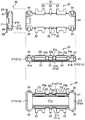
이하, 본 발명의 실시형태에 대해서 도면을 참조하면서 상세하게 설명한다. 또한, 이하에서는, 커넥터(헤더측 하우징 및 소켓측 하우징)의 길이방향을 X 방향, 커넥터(헤더측 하우징 및 소켓측 하우징)의 폭방향(단변방향)을 Y 방향, 도 29 내지 도 32에 있어서의 커넥터의 상하방향을 Z 방향으로 하여 설명한다. 또한, 소켓 및 헤더는, 도 29 내지 도 32에 도시하는 상태에 있어서의 상측을 상하방향 상측(표면측), 하측을 상하방향 하측(이면측)으로 하여 설명한다.BEST MODE FOR CARRYING OUT THE INVENTION Hereinafter, embodiments of the present invention will be described in detail with reference to the drawings. In the following description, the longitudinal direction of the connector (the header side housing and the socket side housing) is referred to as X direction, the width direction (short side direction) of the connector (header side housing and socket side housing) The vertical direction of the connector of Fig. 29 and 32, the socket and the header are described with reference to the upper side in the vertical direction (the front side) and the lower side in the vertical direction lower side (the back side) in the state shown in Figs.
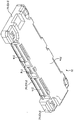
우선, 도 29 내지 도 32를 참조하면서, 본 실시형태에 따른 커넥터(10)의 개요를 설명한다.First, an outline of the
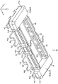
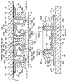
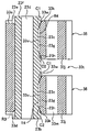
본 실시형태에 따른 커넥터(10)는, 도 29 내지 도 32에 도시하는 바와 같이, 서로 끼워맞춰지는 헤더(20)와 소켓(30)을 구비하고 있다. 본 실시형태에서는, 헤더(20)는 헤더측 신호용 단자(22) 및 헤더측 전원용 단자(23)가 배치되는 헤더 하우징(21)을 갖고 있다. 한편, 소켓(30)은 소켓측 신호용 단자(32) 및 소켓측 전원용 단자(33)가 배치되는 소켓 하우징(31)을 갖고 있다.29 to 32, the
그리고, 헤더 하우징(21)과 소켓 하우징(31)을 끼워맞춤으로써, 헤더측 신호용 단자(22)와 소켓측 신호용 단자(32)를 접촉시키는 동시에, 헤더측 전원용 단자(23)와 소켓측 전원용 단자(33)를 접촉시키도록 하고 있다.The header-
또한, 소켓(30)은 제 2 회로 기판(40)에 장착되는 것이며, 헤더(30)는 제 1 회로 기판(60)에 장착되는 것이다.The
따라서, 헤더(20)와 소켓(30)을 끼워맞추면, 헤더(20)를 장착한 제 2 회로 기판(40)과, 소켓(30)을 장착한 제 1 회로 기판(60)이 전기적으로 접속되게 된다.Therefore, when the
구체적으로는, 본 실시형태에 따른 헤더(20)를 제 2 회로 기판(40) 상에 실장함으로써, 헤더측 신호용 단자(22) 및 헤더측 전원용 단자(23)가 제 2 회로 기판(40) 상의 회로 패턴(41)에 전기적으로 접속되도록 하고 있다. 이러한 제 2 회로 기판(40)으로서는, 프린트 배선 기판(Printed Circuit Board)이나 FPC(Flexible Printed Circuit) 등을 이용할 수 있다.Specifically, by mounting the
또한, 본 실시형태에 따른 소켓(30)을 제 1 회로 기판(60) 상에 실장함으로써, 소켓측 신호용 단자(32) 및 소켓측 전원용 단자(33)가 제 1 회로 기판(60) 상의 회로 패턴(61)에 전기적으로 접속되도록 하고 있다. 이러한 제 1 회로 기판(60)으로서도, 프린트 배선 기판(Printed Circuit Board)이나 FPC(Flexible Printed Circuit) 등을 이용할 수 있다.The socket-
또한, 본 실시형태에 따른 커넥터(10)는, 스마트폰 등의 휴대 단말로서의 전자기기에 있어서의 회로 기판끼리를 전기적으로 접속하는데 이용되는 것이 상정되고 있다. 단, 본 발명의 커넥터는 전자기기에 이용되는 것이라면, 어떠한 부품끼리의 전기적인 접속에 이용되어도 좋다.It is also assumed that the
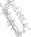
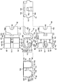
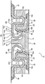
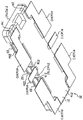
다음에, 도 1 내지 도 14를 참조하면서, 커넥터(10)에 이용되는 헤더(20)의 구성을 설명한다.Next, the configuration of the
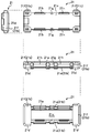
헤더(20)는 상술한 바와 같이 헤더 하우징(21)을 구비하고 있다. 이러한 헤더 하우징(21)은, 본 실시형태에서는, 절연성의 합성 수지에 의해 평면에서 보아 전체적으로 직사각형(장방형) 형상으로 성형되어 있다(도 1 내지 도 6 참조).The
그리고, 헤더 하우징(21)에는, 금속제의 헤더측 신호용 단자(22) 및 금속제의 헤더측 전원용 단자(23)가 배치되어 있다. 헤더측 신호용 단자(22)는 신호선에 전기적으로 접속되어 신호를 전달하는데 이용되는 단자이다. 한편, 헤더측 전원용 단자(23)는 전원선에 전기적으로 접속되어 전원을 공급하는데 이용되는 단자이다.A header-
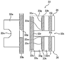
본 실시형태에서는, 헤더 하우징(21)의 한쪽 장변(長邊)을 따라서, 1개의 헤더측 신호용 단자(22)와 2개의 헤더측 전원용 단자(23)가 서로 이격되도록 병설되어 있다. 그리고, 헤더 하우징(21)의 폭방향(단변방향)(Y)의 한쪽측에 병설된 1개의 헤더측 신호용 단자(22) 및 2개의 헤더측 전원용 단자(23)로, 헤더측 단자군(G1)을 구성하고 있다.In this embodiment, one header
또한, 헤더 하우징(21)의 다른쪽 장변을 따라서도, 1개의 헤더측 신호용 단자(22)와 2개의 헤더측 전원용 단자(23)가 서로 이격되도록 병설되어 있다. 그리고, 헤더 하우징(21)의 폭방향(단변방향)(Y)의 다른쪽에 병설된 1개의 헤더측 신호용 단자(22) 및 2개의 헤더측 전원용 단자(23)도, 헤더측 단자군(G1)을 구성하고 있다.Also, one header-
이와 같이, 본 실시형태에서는, 헤더 하우징(21)에는, 해당 헤더 하우징(21)의 길이방향(X)을 따라 배치된 헤더측 신호용 단자(22) 및 헤더측 전원용 단자(23)로 구성되는 헤더측 단자군(G1)이 2열(복수열) 배치되어 있다.As described above, in the present embodiment, the
또한, 1열의 헤더측 단자군(G1)에는, 헤더측 신호용 단자(22)의 양단부에 헤더측 전원용 단자(23)가 각각 배치되어 있다. 환언하면, 헤더측 전원용 단자(23)가 헤더 하우징(21)의 길이방향(X)의 양단부에 배치되는 동시에, 헤더측 전원용 단자(23)의 사이에 헤더측 신호용 단자(22)가 배치되어 있다. 이와 같이, 본 실시형태에서는, 헤더측 신호용 단자(22)보다 헤더 하우징(21)의 길이방향(X)의 외측에 배치되는 헤더측 전원용 단자(23)를 갖고 있다.A header-side
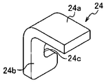
더욱이, 본 실시형태에서는, 헤더 하우징(21)의 길이방향(X)의 양단부에, 금속제의 헤더측 보지 금구(金具)(24)가 배치되어 있다. 이러한 헤더측 보지 금구(24)는 헤더 하우징(21)의 강도를 높이는 동시에, 헤더측 보지 금구(24)가 갖는 고정 단자(24a)를 상술한 제 2 회로 기판(40)에 장착 고정하는데 이용되는 것이다.Furthermore, in this embodiment, a metal-made header-side holding fitting (metal tool) 24 is disposed at both ends of the
다음에, 도 4 내지 도 6을 참조하면서, 헤더 하우징(21)의 구성을 설명한다.Next, the configuration of the
헤더 하우징(21)은, 판형상 벽부(21a)와, 그 주연부를 따라 대략 직사각형 환형상으로 연속적으로 형성되는 주벽부(21b)로 한쪽측(도 5의 하측)이 개구된 대략 상자형상으로 형성되어 있고, 주벽부(21b)의 내부에 오목부(21c)(도 1 참조)가 형성되어 있다. 그리고, 주벽부(21b)의 외주측 하단에는, 외측을 향함에 따라서 상방(판형상 벽부(21a)측)에 위치하도록 경사진 테이퍼부(21d)가 형성되어 있다. 이러한 테이퍼부(21d)는 주벽부(21b)의 길이방향 벽부(21e)의 길이방향 양단부 및 주벽부(21b)의 단변방향 벽부(21f)의 폭방향(Y) 전체에 형성되어 있다. 즉, 헤더 하우징(21)의 길이방향(X) 양단부에, 단변방향 벽부(21f)와 해당 단변방향 벽부(21f)의 폭방향(Y)의 양단부에 연속하는 길이방향 벽부(21e)의 길이방향 단부에서, 평면(이면)에서 보아 대략 U자형의 테이퍼부(21d)가 각각 형성되어 있다.The
또한, 이웃하는 헤더측 신호용 단자(22)와 헤더측 전원용 단자(23) 사이의 주벽부(21b)는 R형(역 U자형)으로 만곡 형성되어 있다.The
또한, 단변방향 벽부(21f)의 폭방향(Y)의 길이가, 대향하는 2개의 길이방향 벽부(21e) 사이의 거리보다 커지도록 형성되어 있고, 헤더 하우징(21)은 전체적으로 평면에서 보다 대략 I자형으로 형성되어 있다.The length of the short
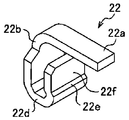
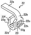
다음에, 도 7a 내지 도 7d, 도 8, 도 9a, 도 9b를 참조하면서, 헤더측 신호용 단자(22)의 구성을 설명한다.Next, the configuration of the header-
헤더측 신호용 단자(22)는 금속 성형에 의해 제조되어 있고, 도전체이다. 그리고, 이 헤더측 신호용 단자(22)는 헤더 하우징(21)의 측면으로부터 돌출하는 베이스부(22a)를 구비하고 있다. 베이스부(22a)는 제 2 회로 기판(40)의 회로 패턴(41)에 땜납(50)에 의해 고정되는 부위이다. 또한, 베이스부(22a)의 상면은, 도 29로부터 알 수 있는 바와 같이, 헤더 하우징(21)의 상면(판형상 벽부(21a)의 외표면)에 대하여 대략 평행하게 연장되어 있다.The header-
또한, 헤더측 신호용 단자(22)는 베이스부(22a)에 연속하는 내측부(22b)를 구비하고 있다. 내측부(22b)는, 헤더 하우징(21)의 판형상 벽부(21a)와 길이방향 벽부(21e)의 접합부를 구부러지면서 관통하고, 길이방향 벽부(21e)의 내표면을 따라 길이방향 벽부(21e)의 선단부까지 연장되어 있다.The header-
그리고, 헤더측 신호용 단자(22)의 내측부(22b)의 내측 표면상에는, 오목부(22c)가 형성되어 있다. 본 실시형태에서는, 오목부(22c)는, 평탄형상의 안쪽면(22g)과, 안쪽면(22g)의 길이방향(X)의 양측에 연설(連設)된 경사면(22h)과, 안쪽면(22g)의 상하방향(Z)의 양측에 연설된 경사면(22i)으로, 대략 사각뿔대 형상으로 형성되어 있다. 이러한 오목부(22c)에는, 후술하는 소켓측 신호용 단자(32)의 원호형상 돌기부(32k)가 끼워넣어진다.A
더욱이, 헤더측 신호용 단자(22)는 내측부(22b)의 한쪽 단부에 연속하는 선단부(22d)를 구비하고 있다. 선단부(22d)는 헤더 하우징(21)의 길이방향 벽부(21e)의 선단의 형상을 따라 구부러져 있다.Furthermore, the header-
헤더측 신호용 단자(22)는 선단부(22d)에 연속하는 피계지부(被係止部)(22e)를 구비하고 있다. 본 실시형태에서는, 피계지부(22e)는 헤더측 신호용 단자(22)에 있어서의 헤더 하우징(21)의 길이방향(X)의 일단부로부터 타단부에 걸쳐서 형성되어 있다. 즉, 헤더측 신호용 단자(22)의 폭방향 전체에 걸쳐서, 단차형상의 피계지부(22e)가 형성되어 있다.The header-
이러한 피계지부(22e)는, 도 29 및 도 30을 대비하면 알 수 있는 바와 같이, 헤더측 신호용 단자(22)가 소켓측 신호용 단자(32)에 끼워넣어질 때에, 단차부로서의 계지부(32d)보다 안쪽으로 삽입된다. 그 때문에, 피계지부(22e)는, 헤더측 신호용 단자(22)가 소켓측 신호용 단자(32)로부터 뽑혀질 때에, 계지부(32d)에 접촉한다. 즉, 헤더측 신호용 단자(22)의 피계지부(22e)는 소켓측 신호용 단자(32)의 계지부(32d)에 의해 계지된다. 따라서, 헤더측 신호용 단자(22)의 소켓측 신호용 단자(32)로부터 뽑혀지는 것이 억제되고 있다. 즉, 헤더측 신호용 단자(22)는, 소정값보다 작은 외력을 가한 것만으로는, 소켓측 신호용 단자(32)로부터 뽑혀질 수 없다. 한편, 헤더측 신호용 단자(22)는, 소정값 이상의 큰 외력을 가하면, 소켓측 신호용 단자(32)로부터 뽑혀질 수 있다. 즉, 헤더측 신호용 단자(22)의 피계지부(22e) 및 소켓측 신호용 단자(32)의 계지부(32d)는, 소정값 이상의 외력을 가하는 것에 의해, 서로의 계지를 해제하는 것이 가능한 로크 기구(locking mechanism)를 구성하고 있다.29 and 30, when the header-
피계지부(22e)는 헤더측 신호용 단자(22)의 두께를 부분적으로 상이하게 하는 모재의 압연에 의해 제조되어도 좋지만, 헤더측 신호용 단자(22)의 모재를 두께 방향으로 구부리는 성형에 의해 제조되어도 좋다.The
더욱이, 헤더측 신호용 단자(22)는 피계지부(22e)를 거쳐서 선단부(22d)에 연속하고, 길이방향 벽부(21e)의 외표면을 따라 연장되는 외측부(22f)를 구비하고 있다. 본 실시형태에서는, 길이방향 벽부(21e)(주벽부(21b))의 외주에 돌출된 돌출 벽부(21g)에 의해, 헤더측 신호용 단자(22)의 외측부(22f) 선단의 위치결정이 이루어지고 있다.The header-
이러한 헤더측 신호용 단자(22)는 소정 두께를 가진 띠형상의 금속재를 만곡 형성하는 것에 의해 형성할 수 있다.The header-
또한, 본 실시형태에서는, 헤더측 신호용 단자(22)는 인서트 성형(insert molding)에 의해 헤더 하우징(21)에 배치되도록 하고 있다. 또한, 헤더측 신호용 단자(22)를 헤더 하우징(21)에 압입함으로써, 헤더측 신호용 단자(22)를 헤더 하우징(21)에 배치시키도록 해도 좋다.Further, in the present embodiment, the header-
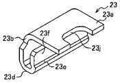
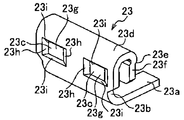
다음에, 도 10a 내지 도 10d, 도 11, 도 12a, 도 12b를 참조하면서, 헤더측 전원용 단자(23)의 구성을 설명한다.Next, the configuration of the header-side
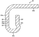
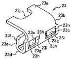
헤더측 전원용 단자(23)는 금속 성형에 의해 제조되어 있고, 도전체이다. 그리고, 이 헤더측 전원용 단자(23)는 헤더 하우징(21)의 측면으로부터 돌출하는 베이스부(23a)를 구비하고 있다. 베이스부(23a)는 제 2 회로 기판(40)의 회로 패턴(41)에 땜납(50)에 의해 고정되는 부위이다. 또한, 베이스부(23a)의 상면은, 도 31로부터 알 수 있는 바와 같이, 헤더 하우징(21)의 상면(판형상 벽부(21a)의 외표면)에 대하여 대략 평행하게 연장되어 있다.The header-side
또한, 헤더측 전원용 단자(23)는 베이스부(23a)에 연속하는 내측부(23b)를 구비하고 있다. 내측부(23b)는, 헤더 하우징(21)의 판형상 벽부(21a)와 길이방향 벽부(21e)의 접합부를 구부러지면서 관통하고, 길이방향 벽부(21e)의 내표면을 따라 길이방향 벽부(21e)의 선단부까지 연장되어 있다.The header-side
그리고, 헤더측 전원용 단자(23)의 내측부(23b)의 내측 표면상에는, 오목부(23c)가 형성되어 있다. 본 실시형태에서는, 오목부(23c)는, 평탄형상의 안쪽면(23g)과, 안쪽면(23g)의 길이방향(X)의 양측에 연설된 경사면(23h)과, 안쪽면(23g)의 상하방향(Z)의 양측에 연설된 경사면(23i)으로, 대략 사각뿔대 형상으로 형성되어 있다. 이러한 오목부(23c)에는, 후술하는 소켓측 전원용 단자(33)의 원호형상 돌기부(33k)가 끼워넣어진다.On the inner surface of the
더욱이, 헤더측 전원용 단자(23)는 내측부(23b)의 한쪽 단부에 연속하는 선단부(23d)를 구비하고 있다. 선단부(23d)는 헤더 하우징(21)의 길이방향 벽부(21e)의 선단의 형상을 따라 구부러져 있다.Furthermore, the header-side
헤더측 전원용 단자(23)는 선단부(23d)에 연속하는 피계지부(23e)를 구비하고 있다. 도 31 및 도 32를 대비하면 알 수 있는 바와 같이, 피계지부(23e)는, 헤더측 전원용 단자(23)가 소켓측 전원용 단자(33)에 끼워넣어질 때에, 단차부로서의 계지부(33d)보다 안쪽으로 삽입된다. 그 때문에, 피계지부(23e)는, 헤더측 전원용 단자(23)가 소켓측 전원용 단자(33)로부터 뽑혀질 때에, 계지부(33d)에 접촉한다. 즉, 헤더측 전원용 단자(23)의 피계지부(23e)는 소켓측 전원용 단자(33)의 계지부(33d)에 의해 계지된다. 따라서, 헤더측 전원용 단자(23)의 소켓측 전원용 단자(33)로부터 뽑혀지는 것이 억제되고 있다. 즉, 헤더측 전원용 단자(23)는, 소정값보다 작은 외력을 가한 것만으로는, 소켓측 전원용 단자(33)로부터 뽑혀질 수 없다. 한편, 헤더측 전원용 단자(23)는, 소정값 이상의 큰 외력을 가하면, 소켓측 전원용 단자(33)로부터 뽑혀질 수 있다. 즉, 헤더측 전원용 단자(23)의 피계지부(23e) 및 소켓측 전원용 단자(33)의 계지부(33d)는, 소정값 이상의 외력을 가하는 것에 의해, 서로의 계지를 해제하는 것이 가능한 로크 기구를 구성하고 있다.The header-side
피계지부(23e)는 헤더측 전원용 단자(23)의 두께를 부분적으로 상이하게 하는 모재의 압연에 의해 제조되어도 좋지만, 헤더측 전원용 단자(23)의 모재를 두께 방향으로 구부리는 성형에 의해 제조되어도 좋다.The
더욱이, 헤더측 전원용 단자(23)는 피계지부(23e)를 거쳐서 선단부(23d)에 연속하고, 길이방향 벽부(21e)의 외표면을 따라 연장되는 외측부(23f)를 구비하고 있다. 더욱이, 본 실시형태에서는, 길이방향 벽부(21e)(주벽부(21b))의 외주에 돌출된 돌출 벽부(21h)에 의해, 헤더측 전원용 단자(23)의 외측부(23f) 선단의 위치 결정이 이루어지고 있다.The header-side
이와 같이, 본 실시형태에서는, 헤더측 신호용 단자(22)의 측단면 형상과 헤더측 전원용 단자(23)의 측단면 형상이 대략 동일 형상을 하고 있다(도 9a 및 도 12a 참조).As described above, in the present embodiment, the side cross-sectional shape of the header-
또한, 상술한 바와 같이, 헤더측 신호용 단자(22) 및 헤더측 전원용 단자(23)는 헤더 하우징(21)의 길이방향(X)을 따라 배치되어 있다. 그리고, 본 실시형태에서는, 헤더측 전원용 단자(23)는 헤더 하우징(21)의 길이방향(X)을 따른 폭이 헤더측 신호용 단자(22)의 길이방향(X)을 따른 폭보다 넓어지도록 형성되어 있다.The header
즉, 본 실시형태에서는, 헤더측 전원용 단자(23)보다 헤더 하우징(21)의 길이방향(X)의 폭이 좁은 헤더측 신호용 단자(22)를 갖도록 하고 있다. 또한, 본 실시형태에서는, 모든 헤더측 신호용 단자(22)가 헤더측 전원용 단자(23)보다 헤더 하우징(21)의 길이방향(X)의 폭이 좁게 되어 있다.That is, in the present embodiment, the header-
이와 같이, 헤더측 전원용 단자(23)에 있어서의 헤더 하우징(21)의 길이방향(X)을 따른 폭을 넓게 하고 있기 때문에, 베이스부(23a)의 길이방향(X) 중앙부에, 오목형상으로 절결된 형상을 한 오목부(23j)를 형성하고 있다. 이러한 오목부(23j)를 형성함으로써, 베이스부(23a)의 돌출량의 증가를 억제하면서, 베이스부(23a)의 회로 패턴에 접하는 윤곽선의 길이를 길게 할 수 있다. 또한, 윤곽선의 형상을 보다 복잡한 형상이 되도록 할 수 있다. 이와 같이 함으로써, 오목부(23j)를 형성하지 않을 경우에 비하여, 넓은 폭의 헤더측 전원용 단자(23)를 제 2 회로 기판(40)의 회로 패턴(41)에 땜납(50)에 의해 고정할 때의, 베이스부(23a)와 회로 패턴(41)의 땜납(50)에 의한 고정 강도가 높아진다.As described above, since the width along the longitudinal direction X of the
또한, 헤더측 전원용 단자(23)의 내측부(23b)의 내측 표면 상에는, 길이방향(X)을 따라 2개의 오목부(23c)가 형성되어 있고, 후술하는 소켓측 전원용 단자(33)의 2개의 원호형상 돌기부(33k)가 각각 끼워넣어지도록 되어 있다.Two
더욱이, 본 실시형태에서는, 피계지부(23e)가 헤더측 전원용 단자(23)에 있어서의 헤더 하우징(21)의 길이방향(X)의 일단부로부터 타단부에 걸쳐서 형성되어 있다. 즉, 넓은 폭의 헤더측 전원용 단자(23)의 폭방향 전체에 걸쳐서, 단차형상의 피계지부(23e)를 형성하고 있다. 이와 같이 함으로써, 헤더측 전원용 단자(23)의 피계지부(23e) 및 소켓측 전원용 단자(33)의 계지부(33d)에 의한 로킹력을 향상시킬 수 있다. 또한, 헤더(20) 및 소켓(30)의 삽탈을 반복했을 때에도, 피계지부(23e)가 마모되기 어려워지기 때문에, 제품의 장수명화를 도모하는 것이 가능해진다.Furthermore, in the present embodiment, the to-
이러한 헤더측 전원용 단자(23)는 소정 두께를 가진 띠형상의 금속재를 만곡 형성하는 것에 의해 형성할 수 있다.The header-side
또한, 본 실시형태에서는, 헤더측 전원용 단자(23)는 인서트 성형에 의해 헤더 하우징(21)에 배치되도록 하고 있다. 또한, 헤더측 전원용 단자(23)를 헤더 하우징(21)에 압입함으로써, 헤더측 전원용 단자(23)를 헤더 하우징(21)에 배치시키도록 해도 좋다.In the present embodiment, the header-side
다음에, 도 13a 내지 도 13d 및 도 14를 참조하면서, 헤더측 보지 금구(24)의 구성을 설명한다.Next, the configuration of the header side holding fitting 24 will be described with reference to Figs. 13A to 13D and Fig.
헤더측 보지 금구(24)는 헤더측 신호용 단자(22)나 헤더측 전원용 단자(23)와 마찬가지로 금속 성형에 의해 제조되어 있다.The header side holding metal fitting 24 is manufactured by metal molding in the same manner as the header
헤더측 보지 금구(24)는 헤더 하우징(21)의 측면으로부터 돌출하는 고정 단자(24a)를 구비하고 있다. 고정 단자(24a)는 제 2 회로 기판(40)의 회로 패턴(41)에 땜납(50)에 의해 고정되는 부위이다. 또한, 고정 단자(24a)의 상면도, 헤더 하우징(21)의 상면(판형상 벽부(21a)의 외표면)에 대하여 대략 평행하게 연장되어 있다.The header side holding metal fitting 24 has a fixed terminal 24a projecting from the side surface of the
또한, 헤더측 보지 금구(24)는 고정 단자(24a)에 연속하는 내측부(24b)를 구비하고 있다. 이 내측부(24b)에는, 길이방향(X)의 한쪽측으로 개구된 절결부(24c)가 형성되어 있다. 이러한 절결부(24c)를 내측부(24b)에 형성함으로써, 헤더 하우징(21)과 헤더측 보지 금구(24)를 보다 밀착시킬 수 있게 되어, 헤더 하우징(21)의 강도를 보다 높일 수 있다.The header side holding metal fitting 24 has an
또한, 본 실시형태에서는, 헤더측 보지 금구(24)는 인서트 성형에 의해 헤더 하우징(21)에 배치되도록 하고 있다. 또한, 헤더측 보지 금구(24)를 헤더 하우징(21)에 압입함으로써, 헤더측 보지 금구(24)를 헤더 하우징(21)에 배치시키도록 해도 좋다.Further, in the present embodiment, the header
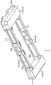
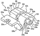
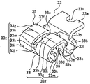
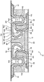
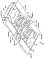
다음에, 도 15 내지 도 28을 이용하여 커넥터(10)에 이용되는 소켓(30)의 구성을 설명한다.Next, the configuration of the
소켓(30)은 상술한 바와 같이 소켓 하우징(31)을 구비하고 있다. 이러한 소켓 하우징(31)은, 본 실시형태에서는, 절연성의 합성 수지에 의해 평면에서 보아 전체적으로 직사각형(장방형) 형상으로 성형되어 있다(도 15 내지 도 20 참조).The
그리고, 소켓 하우징(31)에는, 금속제의 소켓측 신호용 단자(32) 및 금속제의 소켓측 전원용 단자(33)가 배치되어 있다. 소켓측 신호용 단자(32)는 신호선에 전기적으로 접속되어 신호를 전달하는데 이용되는 단자이다. 한편, 소켓측 전원용 단자(33)는 전원선에 전기적으로 접속되어 전원을 공급하는데 이용되는 단자이다.In the
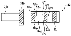
본 실시형태에서는, 소켓 하우징(31)의 한쪽 장변을 따라서, 1개의 소켓측 신호용 단자(32)와 2개의 소켓측 전원용 단자(33)가 서로 이격되도록 병설되어 있다. 그리고, 소켓 하우징(31)의 폭방향(단변방향)(Y)의 한쪽측에 병설된 1개의 소켓측 신호용 단자(32) 및 2개의 소켓측 전원용 단자(33)로, 소켓측 단자군(G2)을 구성하고 있다.In the present embodiment, one socket-
또한, 소켓 하우징(31)의 다른쪽 장변을 따라서도, 1개의 소켓측 신호용 단자(32)와 2개의 소켓측 전원용 단자(33)가 서로 이격되도록 병설되어 있다. 그리고, 소켓 하우징(31)의 폭방향(단변방향)(Y)의 다른쪽측에 병설된 1개의 소켓측 신호용 단자(32) 및 2개의 소켓측 전원용 단자(33)도, 소켓측 단자군(G2)을 구성하고 있다.Further, one socket-
이와 같이, 본 실시형태에서는, 소켓 하우징(31)에는, 해당 소켓 하우징(31)의 길이방향(X)을 따라 배치된 소켓측 신호용 단자(32) 및 소켓측 전원용 단자(33)로 구성되는 소켓측 단자군(G2)이 2열(복수열) 배치되어 있다.As described above, in the present embodiment, the
또한, 1열의 소켓측 단자군(G2)에는, 소켓측 신호용 단자(32)의 양단부에 소켓측 전원용 단자(33)가 각각 배치되어 있다. 환언하면, 소켓측 전원용 단자(33)가 소켓 하우징(31)의 길이방향(X)의 양단부에 배치되는 동시에, 소켓측 전원용 단자(33)의 사이에 소켓측 신호용 단자(32)가 배치되어 있다. 이와 같이, 본 실시형태에서는, 소켓측 신호용 단자(32)보다 소켓 하우징(31)의 길이방향(X)의 외측에 배치되는 소켓측 전원용 단자(33)를 갖고 있다.In the socket-side terminal group G2 of the first row, socket-side
또한, 소켓측 신호용 단자(32) 및 소켓측 전원용 단자(33)는, 헤더(20)와 소켓(30)을 끼워맞췄을 때에, 대응하는 헤더측 신호용 단자(22) 및 헤더측 전원용 단자(23)에 각각 접촉하도록, 소켓 하우징(31)에 배치되어 있다.The socket
더욱이, 본 실시형태에서는, 소켓 하우징(31)의 길이방향(X)의 양단부에, 금속제의 소켓측 보지 금구(34)가 배치되어 있다. 이러한 소켓측 보지 금구(34)는 소켓 하우징(31)의 강도를 높이는 동시에, 소켓측 보지 금구(34)가 갖는 고정 단자(34d)를 상술한 제 1 회로 기판(60)에 장착 고정하는데 이용되는 것이다.In the present embodiment, metal socket-
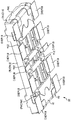
다음에, 도 18 내지 도 20을 참조하면서, 소켓 하우징(31)의 구성을 설명한다.Next, the configuration of the
소켓 하우징(31)은, 판형상 벽부(31a)와, 그 주연부를 따라 대략 직사각형 환형상으로 연속적으로 형성되는 주벽부(31b)로 한쪽측(도 15의 상측)이 개구된 대략 상자형상으로 형성되어 있다. 더욱이, 본 실시형태에서는, 판형상 벽부(31a)의 중앙부에, 주벽부(31b)로부터 소정 간격을 두고서 대략 직사각형 형상의 섬부(31c)가 형성되어 있다. 그리고, 이들 주벽부(31b)와 섬부(31c) 사이에 헤더(20)의 주벽부(21b)를 끼워맞추기 위한 대략 프레임형상의 끼워맞춤 홈부(31d)가 형성되어 있다. 또한, 섬부(31c)는 오목부(21c)에 끼워맞춰진다.The
또한, 끼워맞춤 홈부(31d)에는, 단변방향 벽부(21f) 및 길이방향 벽부(21e)가 끼워맞춰지기 위해서, 끼워맞춤 홈부(31d)는 길이방향(Y)의 양단부가 폭이 넓게 되도록 형성되어 있다.The
더욱이, 본 실시형태에서는, 주벽부(31b)의 내주측 상단에, 내측을 향함에 따라서 하방(판형상 벽부(31a)측)에 위치하도록 경사진 테이퍼부(31e)가 형성되어 있다. 이러한 테이퍼부(31e)는 주벽부(31b)의 길이방향 벽부(31h)의 길이방향 양단부 및 주벽부(31b)의 단변방향 벽부(31i)에 형성되어 있다. 또한, 이웃하는 소켓측 신호용 단자(32)와 소켓측 전원용 단자(33) 사이의 주벽부(31b)에도 테이퍼부(31e)가 형성되어 있다. 이와 같이, 본 실시형태에서는, 주벽부(31b)의 대략 전체 둘레에 걸쳐서 테이퍼부(31e)가 형성되어 있다.Furthermore, in the present embodiment, a tapered
또한, 본 실시형태에서는, 소켓 하우징(31)에는, 소켓측 신호용 단자(32)가 수용되는 소켓측 신호용 단자 수용부(31f)가 판형상 벽부(31a)를 관통하도록 형성되어 있다(도 18 내지 도 20 참조). 또한, 소켓 하우징(31)에는, 소켓측 전원용 단자(33)가 수용되는 소켓측 전원용 단자 수용부(31g)가 판형상 벽부(31a)를 관통하도록 형성되어 있다.In this embodiment, a socket-side signal receiving
소켓측 신호용 단자 수용부(31f)는, 길이방향 벽부(31h)에 소켓측 신호용 단자 수용 오목부(31j)를 끼워맞춤 홈부(31d)와 연통하도록 형성하는 동시에, 섬부(31c)에 소켓측 신호용 단자 수용 오목부(31m)를 끼워맞춤 홈부(31d)와 연통하도록 형성함으로써, 형성되어 있다.The socket-side signal receiving
또한, 소켓측 전원용 단자 수용부(31g)는, 길이방향 벽부(31h)에 소켓측 전원용 단자 수용 오목부(31k)를 끼워맞춤 홈부(31d)와 연통하도록 형성하는 동시에, 섬부(31c)에 소켓측 전원용 단자 수용 오목부(31n)를 끼워맞춤 홈부(31d)와 연통하도록 형성함으로써, 형성되어 있다.The socket-side power
그리고, 소켓측 신호용 단자(32) 및 소켓측 전원용 단자(33)는, 소켓 하우징(31)의 이면측으로부터 소켓측 신호용 단자 수용부(31f) 및 소켓측 전원용 단자 수용부(31g)에 각각 압입된다.The socket-
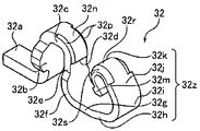
다음에, 도 21a 내지 도 21d, 도 22, 도 23a, 도 23b를 참조하면서, 소켓측 신호용 단자(32)의 구성을 설명한다.Next, the configuration of the socket-
소켓측 신호용 단자(32)는 금속 성형에 의해 제조되어 있고, 도전체이다. 그리고, 이 소켓측 신호용 단자(32)는 소켓 하우징(31)의 측면으로부터 돌출하는 베이스부(32a)를 구비하고 있다. 베이스부(32a)는 제 1 회로 기판(60)의 회로 패턴(61)에 땜납(70)에 의해 고정되는 부위이다. 또한, 베이스부(32a)의 하면은, 제 1 회로 기판(60)의 주 표면(M)을 따라 연장되고, 소켓 하우징(31)의 저면(판형상 벽부(31a)의 이면)과 동일 평면 내에 위치 부여되어 있다.The socket-
소켓측 신호용 단자(32)는, 베이스부(32a)로부터 세워지고, 제 1 회로 기판(60)으로부터 멀어지도록 연장되는 입상부(立上部)(32b)를 구비하고 있다. 입상부(32b)는 베이스부(32a)로부터 구부러져서 소켓측 신호용 단자 수용 오목부(31j) 내로 들어가고, 길이방향 벽부(31h)의 내표면을 따라 연장되어 있다.The socket-
소켓측 신호용 단자(32)는 입상부(32b)의 상단에 그 한쪽 단부가 연속하는 반전 U자형상부(32c)를 구비하고 있다. 반전 U자형상부(32c)는 문자 「U」가 상하 반대로 배치된 형상을 갖고 있다. 또한, 반전 U자형상부(32c)는, 선단면(32n)과, 해당 선단면(32n)의 길이방향(X) 양측에 연설되는 경사면(32p)을 갖고 있고, 수평 단면에서 보아 대략 사다리꼴 형상으로 돌출하는 돌출형상으로 형성되어 있다(도 23b 참조).The socket-
소켓측 신호용 단자(32)는 반전 U자형상부(32c)의 다른쪽 단부에 연속하는 계지부(32d)를 구비하고 있다. 본 실시형태에서는, 계지부(32d)는 소켓측 신호용 단자(32)에 있어서의 소켓 하우징(31)의 길이방향(X)의 일단부로부터 타단부에 걸쳐서 형성되어 있다. 즉, 소켓측 신호용 단자(32)의 폭방향 전체에 걸쳐서, 단차형상의 계지부(32d)가 형성되어 있다.The socket-
이러한 계지부(32d)는, 상술한 바와 같이, 헤더측 신호용 단자(22)가 소켓측 신호용 단자(32)로부터 뽑혀질 때에, 피계지부(22e)의 이동을 억제하는 부분으로서 기능한다. 즉, 소켓측 신호용 단자(32)의 계지부(32d)는 헤더측 신호용 단자(22)의 피계지부(22e)에 접촉하고, 피계지부(22e)를 계지할 수 있다. 소켓측 신호용 단자(32)의 계지부(32d) 및 헤더측 신호용 단자(22)의 피계지부(22e)는, 소정값 이상의 외력을 가하는 것에 의해, 계지를 해제하는 것이 가능한 로크 기구를 구성하고 있다.The locking
계지부(32d)는 소켓측 신호용 단자(32)의 두께를 부분적으로 상이하게 하는 모재의 압연에 의해 제조되어도 좋지만, 소켓측 신호용 단자(32)의 모재를 두께 방향으로 구부리는 성형에 의해 제조되어도 좋다.The locking
또한, 소켓측 신호용 단자(32)는 계지부(32d)에 연속하고, 입상부(32b)에 대략 평행하게 연장되는 입하부(立下部)(32e)를 갖고 있다.The socket-
그리고, 소켓측 신호용 단자(32)는 입하부(32e)의 하단에 연속하는 제 1 원호형상부(32f)를 구비하고 있다.The socket-
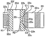
소켓측 신호용 단자(32)는, 도 29 및 도 30에 도시하는 바와 같이, 제 1 원호형상부(32f)에 연속하는 대향부(32z)를 구비하고 있다. 대향부(32z)는, 다음에 설명하는 평탄부(32g), 제 1 경사부(32h), 제 2 원호형상부(32i), 제 2 경사부(32j), 원호형상 돌기부(32k) 및 선단부(32m)를 포함하고 있다. 대향부(32z)는 구체적으로는 다음과 같은 것이다.As shown in Figs. 29 and 30, the socket-
대향부(32z)는 원호형상부(32f)의 하단에 연속하는 평탄부(32g)를 구비하고 있다. 평탄부(32g)는, 도 29에 도시하는 바와 같이, 입하부(32e)로부터 멀어지도록 제 1 회로 기판(60)의 주 표면(M)을 따라 연장되어 있다. 단, 평탄부(32g)는 주 표면(M)에 평행할 필요는 없다. 평탄부(32g)는 후술하는 스프링부의 스프링 길이를 크게 하기 위해 마련되어 있다.The opposing
대향부(32z)는, 도 29에 도시하는 바와 같이, 평탄부(32g)에 연속하고, 제 1 회로 기판(60)의 주 표면(M)에 대하여 경사 방향으로 연장되는 제 1 경사부(32h)를 구비하고 있다. 제 1 경사부(32h)는 제 1 회로 기판(60)으로부터 멀어짐에 따라서, 입하부(32e)로부터 멀어지도록 연장되어 있다. 제 1 경사부(32h)는 제 2 원호형상부(32i)에 연속하고 있다. 제 2 원호형상부(32i)는 입하부(32e)로부터 멀어지도록 돌출하는 만곡부이다. 제 2 원호형상부(32i)는, 제 1 회로 기판(60)의 주 표면(M)에 대하여 경사 방향으로 연장되는 제 2 경사부(32j)에 연속하고 있다. 제 2 경사부(32j)는 제 1 회로 기판(60)으로부터 멀어짐에 따라서, 입하부(32e)에 근접하도록 연장되어 있다. 따라서, 제 2 경사부(32j)는 제 1 경사부(32h)의 상방에 위치 부여되어 있다.29, the opposing
대향부(32z)는, 도 29에 도시하는 바와 같이, 제 2 경사부(32j)의 상단에, 그 한쪽 단부가 연속하는 원호형상 돌기부(32k)를 구비하고 있다. 원호형상 돌기부(32k)는, 선단면(32r)과, 해당 선단면(32r)의 길이방향(X) 양측에 연설되는 경사면(32s)을 갖고 있고, 수평 단면에서 보아 대략 사다리꼴 형상으로 돌출하는 돌출형상으로 형성되어 있다(도 26b 참조).As shown in Fig. 29, the opposing
이러한 원호형상 돌기부(32k)는, 도 29에 도시하는 바와 같이, 헤더측 신호용 단자(22)의 오목부(22c)에 끼워넣어진다. 원호형상 돌기부(32k)의 다른쪽 단부는 선단부(32m)에 연속하고 있다. 선단부(32m)는 제 2 경사부(32j)에 대략 평행하게 연장되어 있다. 도 29 및 도 30으로부터 알 수 있는 바와 같이, 대향부(32z(32g, 32h, 32i, 32j, 32k, 32m))는 원호형상 경사부(32f)의 하단에 연속하고, 전체로서 입하부(32e)에 대향하고 있다.The
본 실시형태에 있어서는, 헤더(20)와 소켓(30)이 끼워맞춰질 때에는, 도 30에 도시하는 바와 같이, 헤더측 신호용 단자(22)는 반전 U자형상부(32c)와 원호형상 돌기부(32k) 사이에 삽입된다. 이 때, 입하부(32e), 원호형상부(32f), 평탄부(32g), 제 1 경사부(32h), 원호형상부(32i), 제 2 경사부(32j), 원호형상 돌기부(32k) 및 선단부(32m)는 일체가 되어서 스프링부로서 기능한다. 스프링부(32e, 32f, 32g, 32h, 32i, 32j, 32k, 32m)는 헤더측 신호용 단자(22)의 볼록부가 소켓측 신호용 단자(32)의 오목부에 삽입되면, 탄성 변형한다. 그것에 의해, 입하부(32e) 및 반전 U자형상부(32c)의 2개의 부분과 원호형상 돌기부(32k) 사이의 거리가 커진다. 이 때, 헤더측 신호용 단자(22)의 피계지부(22e)가 소켓측 신호용 단자(32)의 계지부(32d)보다 하방으로 삽입된다. 그것에 의해, 소켓측 신호용 단자(32)의 원호형상 돌기부(32k)가 헤더측 신호용 단자(22)의 오목부(22c)에 끼워넣어진다.30, the header-
헤더측 신호용 단자(22)가 소켓측 신호용 단자(32)에 끼워맞춰진 상태에서는, 탄성 변형한 스프링부에 복원력이 생긴다. 이러한 복원력에 의해, 원호형상 돌기부(32k)는 헤더측 신호용 단자(22)를 입하부(32e) 및 반전 U자형상부(32c)의 각각에 대하여 가압한다. 그것에 의해, 헤더측 신호용 단자(22)는 소켓측 신호용 단자(32)에 협지(挾持)된다. 이 때, 헤더측 신호용 단자(22)는 소켓측 신호용 단자(32)의 반전 U자형상부(32c), 입하부(32e) 및 원호형상 돌기부(32k)의 각각에 접촉한다.In the state in which the header-
구체적으로는, 도 29 내지 도 33a, 도 33b에 도시하는 바와 같이, 헤더측 신호용 단자(22)의 선단부(22d)가 소켓측 신호용 단자(32)의 입하부(32e)에 접촉한다. 즉, 소켓측 신호용 단자(32)의 접점부(R1) 및 헤더측 신호용 단자(22)의 접점부(R1)가 서로 접촉하게 된다.Specifically, as shown in Figs. 29 to 33A and 33B, the
또한, 헤더측 신호용 단자(22)의 오목부(22c)는 소켓측 신호용 단자(32)의 원호형상 돌기부(32k)에 접촉한다. 즉, 소켓측 신호용 단자(32)의 접점부(R2) 및 헤더측 신호용 단자(22)의 접점부(R2)가 서로 접촉하게 된다.The
이와 같이, 헤더측 신호용 단자(22)와 소켓측 신호용 단자(32)는 폭방향(Y)으로 이격된 복수의 접점(접점부(R1) 및 접점부(R2))에서 접촉한다. 그 때문에, 헤더측 신호용 단자(22)와 소켓측 신호용 단자(32)의 전기적 접속의 신뢰성이 높다.As described above, the header-
더욱이, 본 실시형태에서는, 서로 접촉하는 소켓측 신호용 단자(32)의 접점부(R2) 및 헤더측 신호용 단자(22)의 접점부(R2) 중 어느 한쪽 접점부인 헤더측 신호용 단자(22)의 접점부(R2)에, 오목부(22c)가 형성되어 있다. 그리고, 다른쪽 접점부인 소켓측 신호용 단자(32)의 접점부(R2)가 오목부(22c)에 있어서의 소켓 하우징(31)의 길이방향(X) 양단부에서 접촉하도록 하고 있다.In the present embodiment, the header-
구체적으로는, 도 33a에 도시하는 바와 같이, 소켓측 신호용 단자(32)의 원호형상 돌기부(32k)가 오목부(22c)에 끼워넣어질 때에, 원호형상 돌기부(32k)의 선단면(32r)과 경사면(32s)의 경계 부분이 경사면(22h)에 각각 접촉하고 있다. 이와 같이, 본 실시형태에서는, 소켓측 신호용 단자(32)의 접점부(R2)가 헤더측 신호용 단자(22)의 접점부(R2)에 2점(접점(C1) 및 접점(C2))에서 접촉하도록 하고 있다.More specifically, as shown in Fig. 33A, when the arc-shaped protruding
또한, 스프링부의 탄성 변형에 기인하여, 접점부(R1), 접점부(R2) 이외에, 평탄부(32g)와 제 1 경사부(32h)의 경계부가 제 1 회로 기판(60)에 접점부(R5)에서 접촉하는 경우도 있다.Due to the elastic deformation of the spring portion, the boundary portion between the
이와 같이, 본 실시형태의 헤더측 신호용 단자(22)와 소켓측 신호용 단자(32)는 폭방향(Y)으로 이격된 복수의 접점에서 접하고 있다. 그렇지만, 본 발명의 헤더측 신호용 단자와 소켓측 신호용 단자는, 예를 들어 헤더측 신호용 단자의 내측면과 소켓측 신호용 단자의 대향부의 1 접점에서만 접촉하는 것이어도 좋다.Thus, the header-
또한, 스프링부(32e, 32f, 32g, 32h, 32i, 32j, 32k, 32m)는 U자형상부(32e, 32f, 32g, 32h, 32i, 32j)와, 해당 U자형상부(32e, 32f, 32g, 32h, 32i, 32j)의 일단부(32j측)에 연설된 자유 단부(32k, 32m)로 구성되어 있다. 그리고, 자유 단부(32k, 32m)의 원호형상 돌기부(32k)에, 소켓측 신호용 단자(32)의 접점부(R2)가 마련되어 있다.The
이와 같이, 소켓측 신호용 단자(32)는 U자형상부(32e, 32f, 32g, 32h, 32i, 32j)를 갖고 있고, 해당 U자형상부(32e, 32f, 32g, 32h, 32i, 32j)의 일단부(32j측)에는, 접점부(R2)가 마련되는 자유 단부(32k, 32m)가 연설되어 있다.As described above, the socket-
이러한 소켓측 신호용 단자(32)는 소정 두께를 가진 띠형상의 금속재를 만곡 형성하는 것에 의해 형성할 수 있다.The socket-
또한, 소켓측 신호용 단자(32)는, 소켓(30)을 조립할 때에, 소켓 하우징(31)의 이면측(도 15의 하측)으로부터 소켓측 신호용 단자 수용부(31f)에 삽입(압입)함으로써, 소켓 하우징(31)에 장착되어 있다.The socket-
또한, 소켓측 신호용 단자(32)를 소켓 하우징(31)에 인서트 성형하는 것 등에 의해, 소켓측 신호용 단자(32)를 소켓 하우징(31)에 장착하도록 해도 좋다.The socket-
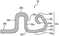
다음에, 도 24a 내지 도 24d, 도 25, 도 26a, 도 26b를 참조하면서, 소켓측 전원용 단자(33)의 구성을 설명한다.Next, the configuration of the socket-side
소켓측 전원용 단자(33)는 금속 성형에 의해 제조되어 있고, 도전체이다. 그리고, 이 소켓측 전원용 단자(33)는 소켓 하우징(31)의 측면으로부터 돌출하는 베이스부(33a)를 구비하고 있다. 베이스부(33a)는 제 1 회로 기판(60)의 회로 패턴(61)에 땜납(70)에 의해 고정되는 부위이다. 또한, 베이스부(33a)의 하면은 제 1 회로 기판(60)의 주 표면(M)을 따라 연장되고, 소켓 하우징(31)의 저면(판형상 벽부(31a)의 이면)과 동일 평면 내에 위치 부여되어 있다.The socket-side
소켓측 전원용 단자(33)는, 베이스부(33a)로부터 세워지고, 제 1 회로 기판(60)으로부터 멀어지도록 연장되는 입상부(33b)를 구비하고 있다. 입상부(33b)는 베이스부(33a)로부터 구부러져서 소켓측 전원용 단자 수용 오목부(31k) 내로 들어가고, 길이방향 벽부(31h)의 내표면을 따라 연장되어 있다.The socket-side
소켓측 전원용 단자(33)는 입상부(33b)의 상단에 그 한쪽 단부가 연속하는 반전 U자형상부(33c)를 구비하고 있다. 반전 U자형상부(33c)는 문자 「U」가 상하 반대로 배치된 형상을 갖고 있다. 또한, 반전 U자형상부(33c)는, 선단면(33r)과, 해당 선단면(33r)의 길이방향(X) 양측에 연설되는 경사면(33s)을 갖고 있고, 수평 단면에서 보아 대략 사다리꼴 형상으로 돌출하는 돌출형상으로 형성되어 있다(도 26b 참조).The socket-side
소켓측 전원용 단자(33)는 반전 U자형상부(33c)의 다른쪽 단부에 연속하는 계지부(33d)를 구비하고 있다. 이 계지부(33d)는, 상술한 바와 같이, 헤더측 전원용 단자(32)가 소켓측 전원용 단자(33)로부터 뽑혀질 때에, 피계지부(23e)의 이동을 억제하는 부분으로서 기능한다. 즉, 소켓측 전원용 단자(33)의 계지부(33d)는 헤더측 전원용 단자(23)의 피계지부(23e)에 접촉하고, 피계지부(23e)를 계지할 수 있다. 소켓측 전원용 단자(33)의 계지부(33d) 및 헤더측 전원용 단자(23)의 피계지부(23e)는, 소정값 이상의 외력을 가하는 것에 의해, 계지를 해제하는 것이 가능한 로크 기구를 구성하고 있다.The socket-side
계지부(33d)는 소켓측 전원용 단자(33)의 두께를 부분적으로 상이하게 하는 모재의 압연에 의해 제조되어도 좋지만, 소켓측 전원용 단자(33)의 모재를 두께 방향으로 구부리는 성형에 의해 제조되어도 좋다.The locking
또한, 소켓측 전원용 단자(33)는 계지부(33d)에 연속하고, 입상부(33b)에 대략 평행하게 연장되는 입하부(33e)를 갖고 있다.The socket-side
그리고, 소켓측 전원용 단자(33)는 입하부(33e)의 하단에 연속하는 제 1 원호형상부(33f)를 구비하고 있다.The socket-side
소켓측 전원용 단자(33)는, 도 31 및 도 32에 도시하는 바와 같이, 제 1 원호형상부(33f)에 연속하는 대향부(33z)를 구비하고 있다. 대향부(33z)는, 다음에 설명하는 평탄부(33g), 제 1 경사부(33h), 제 2 원호형상부(33i), 제 2 경사부(33j), 원호형상 돌기부(33k) 및 선단부(33m)를 포함하고 있다. 대향부(33z)는 구체적으로는 다음과 같은 것이다.As shown in Figs. 31 and 32, the socket-side
대향부(33z)는 원호형상부(33f)의 하단에 연속하는 평탄부(33g)를 구비하고 있다. 평탄부(33g)는, 도 31에 도시하는 바와 같이, 입하부(33e)로부터 멀어지도록 제 1 회로 기판(60)의 주 표면(M)을 따라 연장되어 있다. 단, 평탄부(33g)는 주 표면(M)에 평행할 필요는 없다. 평탄부(33g)는 후술하는 스프링부의 스프링 길이를 크게 하기 위해 마련되어 있다.The opposing
대향부(33z)는, 도 31에 도시하는 바와 같이, 평탄부(33g)에 연속하고, 제 1 회로 기판(60)의 주 표면(M)에 대하여 경사 방향으로 연장되는 제 1 경사부(33h)를 구비하고 있다. 제 1 경사부(33h)는 제 1 회로 기판(60)으로부터 멀어짐에 따라서, 입하부(33e)로부터 멀어지도록 연장되어 있다. 제 1 경사부(33h)는 제 2 원호형상부(33i)에 연속하고 있다. 제 2 원호형상부(33i)는 입하부(33e)로부터 멀어지도록 돌출하는 만곡부이다. 제 2 원호형상부(33i)는 제 1 회로 기판(60)의 주 표면(M)에 대하여 경사 방향으로 연장되는 제 2 경사부(33j)에 연속하고 있다. 제 2 경사부(33j)는 제 1 회로 기판(60)으로부터 멀어짐에 따라서, 입하부(33e)에 근접하도록 연장되어 있다. 따라서, 제 2 경사부(33j)는 제 1 경사부(33h)의 상방에 위치 부여되어 있다.31, the opposing
대향부(33z)는, 도 31에 도시하는 바와 같이, 제 2 경사부(33j)의 상단에, 그 한쪽 단부가 연속하는 원호형상 돌기부(33k)를 구비하고 있다. 원호형상 돌기부(33k)는, 선단면(33v)과, 해당 선단면(33v)의 길이방향(X) 양측에 연설되는 경사면(33w)을 갖고 있고, 수평 단면에서 보아 대략 사다리꼴 형상으로 돌출하는 돌출형상으로 형성되어 있다(도 26b 참조).As shown in Fig. 31, the opposing
이러한 원호형상 돌기부(33k)는, 도 31에 도시하는 바와 같이, 헤더측 전원용 단자(23)의 오목부(23c)에 끼워넣어진다. 원호형상 돌기부(33k)의 다른쪽 단부는 선단부(33m)에 연속하고 있다. 선단부(33m)는 제 2 경사부(33j)에 대략 평행하게 연장되어 있다. 도 31 및 도 32로부터 알 수 있는 바와 같이, 대향부(33z(33g, 33h, 33i, 33j, 33k, 33m))는 원호형상부(33f)의 하단에 연속하고, 전체로서 입하부(33e)에 대향하고 있다.The
본 실시형태에 있어서는, 헤더(20)와 소켓(30)이 끼워맞춰질 때에는, 도 32에 도시하는 바와 같이, 헤더측 전원용 단자(23)는 반전 U자형상부(33c)와 원호형상 돌기부(33k) 사이에 삽입된다. 이 때, 입하부(33e), 원호형상부(33f), 평탄부(33g), 제 1 경사부(33h), 원호형상부(33i), 제 2 경사부(33j), 원호형상 돌기부(33k) 및 선단부(33m)는 일체가 되어서 스프링부로서 기능한다. 스프링부(33e, 33f, 33g, 33h, 33i, 33j, 33k, 33m)는 헤더측 전원용 단자(23)의 볼록부가 소켓측 전원용 단자(33)의 오목부에 삽입되면, 탄성 변형한다. 그것에 의해, 입하부(33e) 및 반전 U자형상부(33c)의 2개의 부분과 원호형상 돌기부(33k) 사이의 거리가 커진다. 이 때, 헤더측 전원용 단자(23)의 피계지부(23e)가 소켓측 전원용 단자(33)의 계지부(33d)보다 하방으로 삽입된다. 그것에 의해, 소켓측 전원용 단자(33)의 원호형상 돌기부(33k)가 헤더측 전원용 단자(23)의 오목부(23c)에 끼워넣어진다.32, when the
헤더측 전원용 단자(23)가 소켓측 전원용 단자(33)에 끼워맞춰진 상태에서는, 탄성 변형한 스프링부에 복원력이 생긴다. 이러한 복원력에 의해, 원호형상 돌기부(33k)는 헤더측 전원용 단자(23)를 입하부(33e) 및 반전 U자형상부(33c)의 각각에 대하여 가압한다. 그것에 의해, 헤더측 전원용 단자(23)는 소켓측 전원용 단자(33)에 협지된다. 이 때, 헤더측 전원용 단자(23)는 소켓측 전원용 단자(33)의 반전 U자형상부(33c), 입하부(33e) 및 원호형상 돌기부(33k)의 각각에 접촉한다.In the state in which the header-side
구체적으로는, 도 31 내지 도 33a, 도 33b에 도시하는 바와 같이, 헤더측 전원용 단자(23)의 선단부(23d)가 소켓측 전원용 단자(33)의 입하부(33e)에 접촉한다. 즉, 소켓측 전원용 단자(33)의 접점부(R3) 및 헤더측 전원용 단자(23)의 접점부(R3)가 서로 접촉하게 된다.Specifically, as shown in Fig. 31 to Fig. 33A and Fig. 33B, the
또한, 헤더측 전원용 단자(23)의 오목부(23c)는 소켓측 전원용 단자(33)의 원호형상 돌기부(33k)에 접촉한다. 즉, 소켓측 전원용 단자(33)의 접점부(R4) 및 헤더측 전원용 단자(23)의 접점부(R4)가 서로 접촉하게 된다.The
이와 같이, 헤더측 전원용 단자(23)와 소켓측 전원용 단자(33)는 폭방향(Y)으로 이격된 복수의 접점(접점부(R3) 및 접점부(R4))에서 접촉한다. 그 때문에, 헤더측 전원용 단자(23)와 소켓측 전원용 단자(33)의 전기적 접속의 신뢰성이 높다.As described above, the header-side
이와 같이, 본 실시형태에서는, 소켓측 신호용 단자(32)의 측단면 형상과 소켓측 전원용 단자(33)의 측단면 형상이 대략 동일 형상을 하고 있다(도 23a 및 도 26a 참조).As described above, in the present embodiment, the side cross-sectional shape of the socket-
또한, 상술한 바와 같이, 소켓측 신호용 단자(32) 및 소켓측 전원용 단자(33)는 소켓 하우징(31)의 길이방향(X)을 따라 배치되어 있다. 그리고, 본 실시형태에서는, 소켓측 전원용 단자(33)는 소켓 하우징(31)의 길이방향(X)을 따른 폭이 소켓측 신호용 단자(32)의 길이방향(X)을 따른 폭보다 넓어지도록 형성되어 있다.The socket-
즉, 본 실시형태에서는, 소켓측 전원용 단자(33)보다 소켓 하우징(31)의 길이방향(X)의 폭이 좁은 소켓측 신호용 단자(32)를 갖도록 하고 있다. 또한, 본 실시형태에서는, 모든 소켓측 신호용 단자(32)가 소켓측 전원용 단자(33)보다 소켓 하우징(31)의 길이방향(X)의 폭이 좁게 되어 있다.That is, in the present embodiment, the socket-
이와 같이, 소켓측 전원용 단자(33)에 있어서의 소켓 하우징(31)의 길이방향(X)을 따른 폭을 넓게 하고 있기 때문에, 베이스부(33a)의 길이방향(X) 중앙부에, 오목형상으로 절결된 형상을 한 오목부(33n)를 형성하고 있다. 이러한 오목부(33n)를 형성함으로써, 베이스부(33a)의 돌출량의 증가를 억제하면서, 베이스부(33a)의 회로 패턴에 접하는 윤곽선의 길이를 길게 할 수 있다. 또한, 윤곽선의 형상을 보다 복잡한 형상이 되도록 할 수 있다. 이와 같이 함으로써, 오목부(33n)를 형성하지 않을 경우에 비하여, 넓은 폭의 소켓측 전원용 단자(33)를 제 1 회로 기판(60)의 회로 패턴(61)에 땜납(70)에 의해 고정할 때의, 베이스부(33a)와 회로 패턴(61)의 땜납(70)에 의한 고정 강도가 높아진다.Since the
또한, 입상부(33b)로부터 반전 U자형상부(33c)에 걸친 길이방향(X)의 중앙부에는, 구멍(33p)이 형성되어 있다. 그리고, 소켓측 전원용 단자(33)를 소켓측 전원용 단자 수용부(31g)에 삽입(압입)했을 때는, 소켓측 전원용 단자 수용 오목부(31k)에 형성된 돌기부(31p)가 구멍(33p)에 삽입되어, 소켓측 전원용 단자(33)가 소켓 하우징(31)에 지지되도록 하고 있다.A
더욱이, 본 실시형태에서는, 계지부(33d)가 소켓측 전원용 단자(33)에 있어서의 소켓 하우징(31)의 길이방향(X)의 일단부로부터 타단부에 걸쳐서 형성되어 있다. 즉, 넓은 폭의 소켓측 전원용 단자(33)의 폭방향 전체에 걸쳐서, 단차형상의 계지부(33d)를 형성하고 있다. 이와 같이 함으로써, 헤더측 전원용 단자(23)의 피계지부(23e) 및 소켓측 전원용 단자(33)의 계지부(33d)에 의한 로킹력을 향상시킬 수 있다. 또한, 헤더(20) 및 소켓(30)의 삽탈을 반복했을 때에도, 계지부(33d)가 마모되기 어려워지기 때문에, 제품의 장수명화를 도모하는 것이 가능해진다.Further, in this embodiment, the locking
더욱이, 본 실시형태에서는, 스프링부(33e, 33f, 33g, 33h, 33i, 33j, 33k, 33m)는 U자형상부(33e, 33f, 33g, 33h, 33i, 33j)와, 해당 U자형상부 (33e, 33f, 33g, 33h, 33i, 33j)의 일단부(33j측)에 연설된 자유 단부(33k, 33m)로 구성되어 있다. 그리고, 자유 단부(33k, 33m)의 원호형상 돌기부(33k)에, 소켓측 전원용 단자(33)의 접점부(R4)가 마련되어 있다.The
이와 같이, 소켓측 전원용 단자(33)는 U자형상부(33e, 33f, 33g, 33h, 33i, 33j)를 갖고 있고, 해당 U자형상부(33e, 33f, 33g, 33h, 33i, 33j)의 일단부(33j측)에는, 접점부(R4)가 마련되는 자유 단부(33k, 33m)가 연설되어 있다.As described above, the socket-side
그리고, 복수의 편부(片部)(35, 36)가 적어도 자유 단부(33k, 33m)에 형성되어 있다.A plurality of
본 실시형태에서는, 스프링부(33e, 33f, 33g, 33h, 33i, 33j, 33k, 33m)의 일부에, 띠형상으로 절결된 형상을 한 홈부(33t)를 형성함으로써, 2개(복수)의 편부(35, 36)를 마련하고 있다.In the present embodiment, the
이러한 2개(복수)의 편부(35, 36)는 가요성을 갖고 있고, 각각 독립하여 휘는 것이 가능하다.The two pieces (pieces) 35 and 36 have flexibility and can be independently bent.
그리고, 2개의 편부(35, 36)의 각각에 접점부(R4)가 마련되어 있다.The contact portions R4 are provided on each of the two
이와 같이, 본 실시형태에서는, 소켓측 전원용 단자(33) 및 헤더측 전원용 단자(23)에는, 서로 접촉하는 접점부(R4)가 복수 마련되어 있다. 구체적으로는, 소켓 하우징(31)의 길이방향(X)을 따라 2개소에 접점부(R4)가 마련되어 있다.As described above, in this embodiment, the socket-side
또한, 본 실시형태에서는, 홈부(33t)의 안쪽부(33u)는 입하부(33e)의 도중에 위치하고 있다. 즉, 홈부(33t)의 안쪽부(33u)는 계지부(33d)보다 자유 단부(33k, 33m)측에 위치하고 있다.In the present embodiment, the
이와 같이 함으로써, 계지부(33d)에 의한 로킹력을 저감시키는 일없이, 자유 단부(33k, 33m)에 스프링성을 갖게 할 수 있게 된다.By doing so, the
또한, 소켓측 전원용 단자 수용 오목부(31n)에는, 칸막이벽(31r)이 형성되어 있다. 그리고, 소켓측 전원용 단자(33)를 소켓측 전원용 단자 수용부(31g)에 삽입(압입)했을 때는, 홈부(33t)에 칸막이벽(31r)이 삽입되어, 2개(복수)의 편부(35, 36)가 서로 간섭해버리는 것을 억제하도록 되어 있다.Further, a
더욱이, 본 실시형태에서는, 서로 접촉하는 소켓측 전원용 단자(33)의 접점부(R4) 및 헤더측 전원용 단자(23)의 접점부(R4) 중 어느 한쪽 접점부인 헤더측 전원용 단자(23)의 접점부(R4)에, 오목부(23c)가 형성되어 있다. 그리고, 다른쪽 접점부인 소켓측 전원용 단자(33)의 접점부(R4)가 오목부(23c)에 있어서의 소켓 하우징(31)의 길이방향(X) 양단부에서 접촉하도록 하고 있다.In the present embodiment, the connection of the header-side
구체적으로는, 도 33b에 도시하는 바와 같이, 소켓측 전원용 단자(33)의 원호형상 돌기부(33k)가 오목부(23c)에 끼워넣어질 때에, 원호형상 돌기부(33k)의 선단면(33v)과 경사면(33w)의 경계 부분이 경사면(23h)에 각각 접촉하고 있다. 이와 같이, 본 실시형태에서는, 소켓측 전원용 단자(33)의 접점부(R4)가 헤더측 전원용 단자(23)의 접점부(R4)에 2점(접점(C1) 및 접점(C2))에서 접촉하도록 하고 있다.Specifically, as shown in Fig. 33B, when the arc-shaped protruding
본 실시형태에서는, 길이방향(X)을 따라 이격되도록 형성된 2개소의 접점부(R4) 모두가 2점(접점(C1) 및 접점(C2))에서 접촉하도록 되어 있다.In this embodiment, all of the two contact points R4 formed to be spaced along the longitudinal direction X are brought into contact at two points (the contact C1 and the contact C2).
또한, 스프링부의 탄성 변형에 기인하여, 접점부(R3), 접점부(R4) 이외에, 평탄부(33g)와 제 1 경사부(33h)의 경계부가 제 1 회로 기판(60)에 접점부(R5)에서 접촉하는 경우도 있다.Due to the elastic deformation of the spring portion, the boundary portion between the
이러한 소켓측 전원용 단자(33)는 소정 두께를 가진 띠형상의 금속재를 만곡 형성하는 것에 의해 형성할 수 있다.The socket-side
또한, 소켓측 전원용 단자(33)는, 소켓(30)을 조립할 때에, 소켓 하우징(31)의 이면측(도 15의 하측)으로부터 소켓측 전원용 단자 수용부(31g)에 삽입(압입)함으로써, 소켓 하우징(31)에 장착되어 있다.The socket-side
또한, 소켓측 전원용 단자(33)를 소켓 하우징(31)에 인서트 성형하는 것 등에 의해, 소켓측 전원용 단자(33)를 소켓 하우징(31)에 장착하도록 해도 좋다.Further, the socket-side
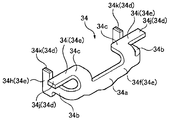
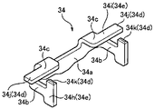
다음에, 도 27a 내지 도 27d 및 도 28을 참조하면서, 소켓측 보지 금구(34)의 구성을 설명한다.Next, the configuration of the socket-
소켓측 보지 금구(34)는, 소정 두께의 금속판을 프레스 성형하는 것에 의해 형성된 보지 금구판을 절곡 형성함으로써 형성할 수 있고, 커넥터(10)의 폭방향(Y)으로 연장되는 측판부(34a)와, 측판부(34a)의 하측을 길이방향(X) 중앙측을 향해서 대략 직각으로 절곡한 저판부(34c)를 구비하고 있다. 그리고, 저판부(34c)의 양단부를 커넥터(10)의 폭방향(Y) 양측으로부터 외측으로 돌출시킴으로써, 고정 단자(34d)로서의 제 1 고정 단자(34j)가 형성되어 있다.The socket-
측판부(34a)의 폭방향(Y) 양단부에는, 측판부(34a)의 폭방향(Y) 양단부를 커넥터(10)의 길이방향(X) 중앙측을 향해서 대략 직각으로 절곡한 연장부(34b)가 형성되어 있다. 그리고, 이 연장부(34b)의 연장 방향의 종착부(34g)에는 하방을 향해서 연장되어 제 1 회로 기판(60)에 땜납(70)으로 고정되는 고정 단자(34d)로서의 제 2 고정 단자(34k)가 마련되어 있다.The
본 실시형태에서는, 근방에 배치되는 제 1 고정 단자(34j) 및 제 2 고정 단자(34k)로 형성되는 고정 단자의 세트가, 커넥터(10)의 한쌍의 장변 각각의 길이방향(X)의 양단부에, 소켓측 단자군(G2)과 병설하도록 합계 4 세트 마련되어 있다.The set of fixed terminals formed by the first fixed
이와 같이, 본 실시형태에서는, 소켓측 보지 금구(34)가, 제 1 회로 기판(60) 상에 고정되는 제 1 고정 단자(34j)와, 해당 제 1 고정 단자(34j)와는 별개로 형성되어 제 1 회로 기판(60) 상에 고정되는 제 2 고정 단자(34k)를 갖고 있다. 그리고, 이 제 2 고정 단자(34k)가 소켓측 보지 금구(34)의 연장부(34b)로부터 연장되어 있다.As described above, in this embodiment, the socket-
이 때, 제 2 고정 단자(34k)가, 세트가 되는 제 1 고정 단자(34j)로부터의 소켓측 보지 금구(34) 상에 있어서의 도정(道程)(소켓측 보지 금구(34)의 외면을 따른 거리)이 최대가 되는 위치에 마련되도록 하고 있다.At this time, the second fixed terminal 34k contacts the outer surface of the socket-side holding fitting 34 on the socket-side holding fitting 34 from the first fixed terminal 34j to be set Is a maximum.
또한, 본 실시형태에서는, 소켓측 보지 금구(34)는 인서트 성형에 의해 소켓 하우징(31)에 장착(배치)되어 있다. 이 때, 소켓측 보지 금구(34)의 적어도 일부가 소켓 하우징(31)을 따라 노출되도록 하고 있다.Further, in the present embodiment, the socket-
즉, 소켓측 보지 금구(34)의 적어도 일부가 소켓 하우징(31)의 외면(31s)을 따라 노출되어 있다.That is, at least a part of the socket-
더욱이, 본 실시형태에서는, 주벽부(31b) 및 판형상 벽부(31a)의 외면(31s)의 일부와 소켓측 보지 금구(34)의 외벽면(34e)의 일부가 대략 면일(面一)의 상태가 되도록 하고 있다. 환언하면, 주벽부(31b)의 외면(31s)에 소켓측 보지 금구(34)의 외벽면(34e)의 일부가 대략 면일의 상태로 노출되도록, 소켓 하우징(31)에 소켓측 보지 금구(34)가 일체 성형되어 있다.In the present embodiment, a part of the
구체적으로는, 측판부(34a)의 외면(34f)의 상부가 소켓 하우징(31)의 X 방향(길이방향) 최외단으로 연장되는 측면(길이방향의 단부면)(31t)에 대하여 면일의 상태로 노출되어 있다. 이와 같이, 본 실시형태에서는, 소켓측 보지 금구(34)는 소켓 하우징(31)의 측면(31t) 및 저면(31u) 중 적어도 어느 한쪽 면을 따라 노출되도록 하고 있다.Concretely, the upper portion of the
또한, 저판부(34c)의 외면(34i)은 소켓 하우징(31)의 저면(31u)(외면(31s))에 대하여 면일의 상태가 아니게 노출되어 있지만, 저판부(34c)의 외면(34i)을, 소켓 하우징(31)의 저면(31u)(외면(31s))에 대하여 면일의 상태로 노출시키는 것도 가능하다. 또한, 소켓측 보지 금구(34)의 외벽면(34e)은 주벽부(31b)의 외면(단변방향 벽부(31i)의 외면(31s))에 노출시킬 필요는 없고, 또한 노출시키는 경우라도, 주벽부(31b)의 외면(단변방향 벽부(31i)의 외면(31s))에 대하여 면일의 상태로 노출시킬 필요는 없다. 또한, 연장부(34b)의 외벽면(34e)(외면(34h))을 주벽부(31b)의 외면(길이방향 벽부(31h)의 외면(31s))으로부터 노출시키는 것도 가능하다. 이 때, 면일의 상태로 노출시켜도 좋고, 면일의 상태가 되지 않도록 노출시켜도 좋다.The
그리고, 도 30 및 도 32에 도시하는 바와 같이, 헤더 하우징(21)의 주벽부(21b)를 소켓 하우징(31)의 끼워맞춤 홈부(31d)에 삽입하여 끼워맞춤으로써, 헤더(20)가 소켓(30)에 끼워맞춰진다.30 and 32, the
또한, 헤더(20)를 소켓(30)에 끼워맞출 때는, 예를 들어 Y 방향(폭방향: 단변방향) 일단측의 장변 부분에 형성된 테이퍼부(31e)와 테이퍼부(21d)를 중첩하고, Y 방향(폭방향: 단변방향) 타단측에 어긋나면서 끼워맞춰지게 하도록 할 수 있다. 이와 같이 하면, 테이퍼부(31e) 및 테이퍼부(21d)를 유인부(guider)로서 기능시킬 수 있어, 보다 용이하게 헤더(20)를 소켓(30)에 끼워맞출 수 있게 된다.When the
그리고, 헤더(20)를 소켓(30)에 끼워맞춘 상태에서는, 소켓측 신호용 단자(32)의 접점부(R1) 및 헤더측 신호용 단자(22)의 접점부(R1)가 서로 접촉하게 된다.The contact portion R1 of the socket
또한, 소켓측 신호용 단자(32)의 접점부(R2) 및 헤더측 신호용 단자(22)의 접점부(R2)가 서로 접촉하게 된다.The contact portion R2 of the socket
그리고, 소켓측 전원용 단자(33)의 접점부(R3) 및 헤더측 전원용 단자(23)의 접점부(R3)가 서로 접촉하게 된다.The contact portion R3 of the socket-side
또한, 소켓측 전원용 단자(33)의 접점부(R4) 및 헤더측 전원용 단자(23)의 접점부(R4)가 서로 접촉하게 된다.The contact portion R4 of the socket-side
그 결과, 소켓측 신호용 단자(32)와 헤더측 신호용 단자(22)가 전기적으로 접속되는 동시에, 소켓측 전원용 단자(33)와 헤더측 전원용 단자(23)가 전기적으로 접속된다.As a result, the socket-
이와 같이 해서, 제 1 회로 기판(60)의 회로 패턴(61)과 제 2 회로 기판(40)의 회로 패턴(41)이 서로 전기적으로 접속되게 된다.In this manner, the
한편, 헤더(20)와 소켓(30)을 이탈시킬 때는, 이들 양자를 박리 방향으로 탈거한다. 그러면, 단차형상의 계지부(32d)와 단차형상의 피계지부(22e)가 상대 미끄럼운동하면서, 소켓측 신호용 단자(32)의 스프링부(32e, 32f, 32g, 32h, 32i, 32j, 32k, 32m)가 탄성 변형하여, 계지부(33d)와 피계지부(23e)의 계지가 해제된다. 이 때, 원호형상 돌기부(32k)의 오목부(22c)에의 끼워넣음도 해제된다.On the other hand, when releasing the
또한, 단차형상의 계지부(33d)와 단차형상의 피계지부(23e)가 상대 미끄럼운동하면서, 소켓측 전원용 단자(33)의 스프링부(33e, 33f, 33g, 33h, 33i, 33j, 33k, 33m)가 탄성 변형하여, 계지부(33d)와 피계지부(23e)의 계지가 해제된다. 이 때, 원호형상 돌기부(33k)의 오목부(23c)에의 끼워넣음도 해제된다.The
이와 같이 해서, 헤더(20)와 소켓(30)을 분리시킬 수 있게 된다.Thus, the
또한, 본 실시형태에서는, 상술한 바와 같이, 헤더 하우징(21)의 길이방향(X) 양단부에는 헤더측 보지 금구(24)가 배치되고, 소켓 하우징(31)의 길이방향(X) 양단부에는 소켓측 보지 금구(34)가 배치되어 있다. 이러한 헤더측 보지 금구(24) 및 소켓측 보지 금구(34)는 헤더 하우징(21) 및 소켓 하우징(31)의 강도를 높이는 동시에, 상술한 회로 기판에 각각 장착 고정하는데 이용되는 것이다.In the present embodiment, as described above, the header
본 실시형태에서는, 헤더측 보지 금구(24)의 고정 단자(24a)를 제 2 회로 기판(40)에 납땜함으로써, 헤더(20)가 제 2 회로 기판(40)에 대하여 강고하게 결합되도록 하고 있다.In this embodiment, the
또한, 소켓측 보지 금구(34)의 고정 단자(34d)를 제 1 회로 기판(60)에 납땜함으로써, 소켓(30)이 제 1 회로 기판(60)에 대하여 강고하게 결합되도록 하고 있다.The
이러한 구성에 따르면, 각 회로 기판에 강고하게 결합된 헤더(20)와 소켓(30)을 서로 끼워맞출 수 있다. 이것에 의해, 헤더측 신호용 단자(22)와 소켓측 신호용 단자(32)가 접촉 도통하는 동시에, 헤더측 전원용 단자(23)와 소켓측 전원용 단자(33)가 접촉 도통하여, 각 회로 기판의 회로 패턴끼리를 전기적으로 접속할 수 있다.According to this configuration, the
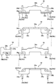
다음에, 도 34 내지 도 37을 참조하면서, 각 단자 및 각 보지 금구의 회로 패턴에의 고정 구조를 설명한다. 또한, 각 단자 및 각 보지 금구의 회로 패턴에의 고정 구조는 도 34 내지 도 37의 구조에 한정되는 것은 아니다.Next, a fixing structure of each terminal and each of the retaining brackets to the circuit pattern will be described with reference to Figs. 34 to 37. Fig. In addition, the fixing structure of each terminal and each of the retaining brackets to the circuit pattern is not limited to the structures shown in Figs.
헤더측 신호용 단자(22), 헤더측 전원용 단자(23) 및 헤더측 보지 금구(24)는 도 34에 도시하는 바와 같이 하여, 회로 패턴(41)에 고정되도록 할 수 있다.The header-
길이방향(X)의 중앙부에 배치된 헤더측 신호용 단자(22)는 베이스부(22a)가 각각 신호용의 회로 패턴(41a)에 땜납(50)으로 고정된다.The header-
한편, 길이방향(X)의 양측에 배치된 헤더측 전원용 단자(23)는 베이스부(23a)가 공통의 회로 패턴(41b)에 땜납(50)으로 고정된다. 그리고, 헤더측 보지 금구(24)도, 고정 단자(24a)가 공통의 회로 패턴(41b)에 땜납(50)으로 고정된다.On the other hand, the header-side
이와 같이, 도 34에서는, 고정 단자(24a)와 베이스부(23a)가 공통의 회로 패턴(41b)에 납땜되어 있다.34, the fixed terminal 24a and the
더욱이, 도 34에서는, 이웃하도록 배치되어 있는 헤더측 전원용 단자(23)와 헤더측 보지 금구(24)가 공통의 회로 패턴(41b)에 납땜되어 있다. 즉, 이웃하도록 배치되어 있는 헤더측 전원용 단자(23)와 헤더측 보지 금구(24)가 회로 패턴(41b)을 공용하고 있다.34, the header-side
따라서, 길이방향(X)의 일측에 배치된 2개의 헤더측 전원용 단자(23)는 길이방향(X)의 일측에 배치된 회로 패턴(41b) 및 길이방향(X)의 일측에 배치된 헤더측 보지 금구(24)를 거쳐서 전기적으로 접속되어 있다. 또한, 길이방향(X)의 타측에 배치된 2개의 헤더측 전원용 단자(23)도, 길이방향(X)의 타측에 배치된 회로 패턴(41b) 및 길이방향(X)의 타측에 배치된 헤더측 보지 금구(24)를 거쳐서 전기적으로 접속되어 있다.Therefore, the two header-side
한편, 소켓측 신호용 단자(32), 소켓측 전원용 단자(33) 및 소켓측 보지 금구(34)는 도 35에 도시하는 바와 같이 하여, 회로 패턴(61)에 고정되도록 할 수 있다.On the other hand, the socket-
길이방향(X)의 중앙부에 배치된 소켓측 신호용 단자(32)는 베이스부(32a)가 각각 신호용의 회로 패턴(61a)에 땜납(70)으로 고정된다.The
길이방향(X)의 양측에 배치된 소켓측 전원용 단자(33)는 베이스부(33a)가 공통의 회로 패턴(61b)에 땜납(70)으로 고정된다. 그리고, 소켓측 보지 금구(34)도, 고정 단자(34d)가 공통의 회로 패턴(61b)에 땜납(70)으로 고정된다.The socket-side
이와 같이, 도 35에서는, 고정 단자(34d)와 베이스부(33a)가 공통의 회로 패턴(61b)에 납땜되어 있다.35, the fixed
더욱이, 도 35에서는, 이웃하도록 배치되어 있는 소켓측 전원용 단자(33)와 소켓측 보지 금구(34)가 공통의 회로 패턴(61b)에 납땜되어 있다. 따라서, 길이방향(X)의 일측에 배치된 2개의 소켓측 전원용 단자(33)는 길이방향(X)의 일측에 배치된 회로 패턴(61b) 및 길이방향(X)의 일측에 배치된 소켓측 보지 금구(34)를 거쳐서 전기적으로 접속되어 있다. 또한, 길이방향(X)의 타측에 배치된 2개의 소켓측 전원용 단자(33)도, 길이방향(X)의 타측에 배치된 회로 패턴(61b) 및 길이방향(X)의 타측에 배치된 소켓측 보지 금구(34)를 거쳐서 전기적으로 접속되어 있다.35, the socket-side
더욱이, 본 실시형태에서는, 서로 세트가 되는 제 1 고정 단자(34j) 및 제 2 고정 단자(34k)가, 베이스부(33a)가 납땜되는 회로 패턴(61b)에 납땜되어 있다.Furthermore, in the present embodiment, the first fixed
또한, 헤더측 신호용 단자(22), 헤더측 전원용 단자(23) 및 헤더측 보지 금구(24)는 도 36에 도시하는 바와 같이 하여, 회로 패턴(41)에 고정되도록 할 수 있다.The header-
길이방향(X)의 중앙부에 배치된 헤더측 신호용 단자(22)는 베이스부(22a)가 각각 신호용의 회로 패턴(41a)에 땜납(50)으로 고정된다.The header-
또한, 길이방향(X)의 양측에 배치된 헤더측 전원용 단자(23)는 베이스부(23a)가 전원용의 회로 패턴(41c)에 땜납(50)으로 고정된다.The header-side
그리고, 헤더측 보지 금구(24)는 고정 단자(24a)가 금구 고정용의 회로 패턴(41d)에 땜납(50)으로 고정된다.The fixed terminal 24a of the header side holding metal fitting 24 is fixed to the
이와 같이, 도 36에서는, 고정 단자(24a)와 베이스부(23a)를 각각 별개의 회로 패턴(41)에 납땜하고 있다.36, the fixed terminal 24a and the
한편, 소켓측 신호용 단자(32), 소켓측 전원용 단자(33) 및 소켓측 보지 금구(34)도, 도 37에 도시하는 바와 같이 하여, 회로 패턴(61)에 고정되도록 할 수 있다.On the other hand, the socket-
길이방향(X)의 중앙부에 배치된 소켓측 신호용 단자(32)는 베이스부(32a)가 각각 신호용의 회로 패턴(61a)에 땜납(70)으로 고정된다.The
또한, 길이방향(X)의 양측에 배치된 소켓측 전원용 단자(33)는 베이스부(33a)가 전원용의 회로 패턴(61c)에 땜납(70)으로 고정된다.The
그리고, 소켓측 보지 금구(34)는 고정 단자(34d)가 금구 고정용의 회로 패턴(61d)에 땜납(70)으로 고정된다.The fixed terminal 34d of the socket side holding fitting 34 is fixed to the
이와 같이, 도 37에서는, 고정 단자(34d)와 베이스부(33a)를 각각 별개의 회로 패턴(61)에 납땜하고 있다.37, the fixed
그리고, 소켓측의 고정 구조로서 도 34와 도 36 중 어느 하나를 선택하고, 헤더측의 고정 구조로서 도 35와 도 37 중 어느 하나를 선택하여, 각각을 조합시킴으로써, 커넥터(10)의 회로 패턴에의 고정 구조를 얻을 수 있다.34 and 36 are selected as the socket-side fixing structure, and either one of Figs. 35 and 37 is selected as the header-side fixing structure, and these are combined to form the circuit pattern of the
이상, 설명한 바와 같이, 본 실시형태의 커넥터(10)는 소켓측 신호용 단자(32) 및 소켓측 전원용 단자(33)가 배치되는 대략 직사각형상의 소켓 하우징(31)을 갖는 소켓(30)과, 헤더측 신호용 단자(22) 및 헤더측 전원용 단자(23)가 배치되는 대략 직사각형상의 헤더 하우징(21)을 갖는 헤더(20)를 구비하고 있다.As described above, the
그리고, 소켓측 신호용 단자(32) 및 소켓측 전원용 단자(33)가 소켓 하우징(31)의 길이방향(X)을 따라 배치되어 있고, 소켓측 전원용 단자(33)보다 소켓 하우징(31)의 길이방향(X)의 폭이 좁은 소켓측 신호용 단자(32)를 갖고 있다.The socket-
이와 같이 하면, 서로 이격 배치되어 있는 복수의 단자를 전원용 단자로서 병용할 경우에 비하여, 사공간(dead space)이 형성되어버리는 것이 억제되기 때문에, 소켓(30)의 길이방향(X)을 소형화하는 것이 가능해진다.In this manner, dead space is prevented from being formed as compared with a case where a plurality of terminals spaced apart from each other are used as a power supply terminal, so that the longitudinal direction X of the
또한, 소켓측 신호용 단자(32)의 단면형상과 소켓측 전원용 단자(33)의 단면형상이 대략 동일 형상을 하고 있다. 그 결과, 부품 가공성이 향상하는 동시에 조립 가공성이 향상한다.In addition, the cross-sectional shape of the socket-
또한, 소켓 하우징(31)에는, 해당 소켓 하우징(31)의 길이방향(X)을 따라 배치된 소켓측 신호용 단자(32) 및 소켓측 전원용 단자(33)로 구성되는 소켓측 단자군(G2)이 복수열 배치되어 있다.The
이와 같이 하면, 단자의 단면적을 증가시킬 수 있기 때문에, 전류 용량을 증가시킬 수 있다.In this case, since the cross-sectional area of the terminal can be increased, the current capacity can be increased.
또한, 소켓측 전원용 단자(33)는 헤더측 전원용 단자(23)에 계지되는 단차형상의 계지부(33d)를 갖고 있고, 계지부(33d)가 소켓측 전원용 단자(33)에 있어서의 소켓 하우징(31)의 길이방향(X)의 일단부로부터 타단부에 걸쳐서 형성되어 있다.The socket-side
그 결과, 로킹력을 향상시킬 수 있는 동시에, 삽탈을 반복했을 때에 마모되기 어려워지기 때문에, 제품의 장수명화를 도모하는 것이 가능해진다.As a result, the locking force can be improved, and wear is less likely to occur when the insertion / removal is repeated, so that it is possible to increase the life span of the product.
또한, 소켓측 신호용 단자(32)보다 소켓 하우징(31)의 길이방향(X)의 외측에 배치되는 소켓측 전원용 단자(33)를 갖고 있다.Side
이와 같이 하면, 발열량이 큰 소켓측 전원용 단자(33)를 소켓 하우징(31)의 길이방향(X)의 외측에 배치시키는 것이기 때문에, 방열 효율을 보다 높일 수 있게 된다.In this case, since the socket-side
또한, 소켓측 전원용 단자(33) 및 헤더측 전원용 단자(23)에는, 서로 접촉하는 접점부(R4)가 소켓 하우징(31)의 길이방향(X)을 따라 복수 마련되어 있다.A plurality of contact portions R4 are provided on the socket-side
이와 같이 하면, 단자의 접촉 신뢰성을 향상시키면서, 접촉 저항의 저감을 도모할 수 있게 된다.In this way, it is possible to reduce the contact resistance while improving the contact reliability of the terminals.
또한, 소켓측 전원용 단자(33)에는, 복수의 편부(35, 36)가 형성되어 있고, 복수의 편부(35, 36)의 각각에 접점부(R4)가 마련되어 있다.The socket-side
이와 같이 함으로써, 단자의 접촉 신뢰성을 향상시키면서, 접촉 저항의 저감을 도모할 수 있게 된다.By doing so, it is possible to reduce the contact resistance while improving the contact reliability of the terminal.
또한, 복수의 편부(35, 36)는 가요성을 갖고 있고, 각각 독립하여 휘는 것이 가능하다.Further, the plurality of
이와 같이 함으로써, 단자의 접촉 신뢰성을 보다 향상시키면서, 접촉 저항의 저감을 도모할 수 있게 된다.In this way, it is possible to reduce the contact resistance while improving the contact reliability of the terminal.
또한, 소켓측 전원용 단자(33)는 U자형상부(33e, 33f, 33g, 33h, 33i, 33j)를 갖고 있다. 이러한 U자형상부(33e, 33f, 33g, 33h, 33i, 33j)의 일단부(33j측)에는, 접점부(R4)가 마련되는 자유 단부(33k, 33m)가 연설되어 있다. 그리고, 복수의 편부(35, 36)가 적어도 자유 단부(33k, 33m)에 형성되어 있다.The socket-side
이와 같이 함으로써, 단자의 접촉 신뢰성을 보다 향상시킬 수 있게 된다.In this way, the contact reliability of the terminal can be further improved.
또한, 서로 접촉하는 소켓측 전원용 단자(33)의 접점부(R4) 및 헤더측 전원용 단자(23)의 접점부(R4) 중 어느 한쪽 접점부(헤더측 전원용 단자(23)의 접점부(R4))에는 오목부(23c)가 형성되어 있다. 그리고, 다른쪽 접점부(소켓측 전원용 단자(33)의 접점부(R4))가 오목부(23c)에 있어서의 소켓 하우징(31)의 길이방향(X) 양단부(접점(C1, C2))에서 접촉한다.The contact portion R4 of the socket-side
이와 같이 함으로써, 단자의 접촉 신뢰성을 보다 향상시킬 수 있게 된다.In this way, the contact reliability of the terminal can be further improved.
또한, 소켓 하우징(31)에는, 소켓측 보지 금구(34)가 배치되어 있고, 소켓측 보지 금구(34)의 적어도 일부(34a, 34c)가 소켓 하우징(31)의 외면(31s)을 따라 노출되어 있다.The socket
이와 같이 함으로써, 소켓 하우징의 소형화를 도모하면서, 소켓 하우징과 소켓측 보지 금구를 보다 강고하게 고정할 수 있다.By doing so, the socket housing and the socket-side retaining bracket can be more firmly fixed while reducing the size of the socket housing.
더욱이, 소켓측 보지 금구(34)는 소켓 하우징(31)의 측면(31t) 및 저면(31u) 중 적어도 어느 한쪽 면을 따라 노출되어 있다.Furthermore, the socket-
따라서, 소켓 하우징의 소형화를 도모하면서, 소켓 하우징과 소켓측 보지 금구를 한층더 강고하게 고정할 수 있게 된다.Therefore, the socket housing and the socket-side retaining bracket can be more firmly fixed while reducing the size of the socket housing.
또한, 소켓측 보지 금구(34)가 인서트 성형에 의해 소켓 하우징(31)에 배치되어 있다.The socket-
그 결과, 소켓 하우징과 소켓측 보지 금구를 보다 강고하게 고정할 수 있는 동시에, 압입했을 경우에 비하여, 소켓 하우징과의 접촉 면적을 증가시킬 수 있기 때문에, 방열성을 높일 수 있게 된다.As a result, the socket housing and the socket-side retaining bracket can be more firmly fixed, and the contact area with the socket housing can be increased as compared with the case where the socket housing and the socket-side retaining bracket are press-fitted.
또한, 소켓측 보지 금구(34)는 제 1 회로 기판(60)에 형성된 회로 패턴(61)에 납땜되는 고정 단자(34d)를 갖고 있다. 그리고, 소켓측 전원용 단자(33)는 제 1 회로 기판(60)에 형성된 회로 패턴(61)에 납땜되는 베이스부(33a)를 갖고 있다. 그리고, 고정 단자(34d)와 베이스부(33a)가 공통의 회로 패턴(61b)에 납땜되어 있다.The socket-
이와 같이 하면, 소켓측 보지 금구(34)가 고정되는 회로 패턴도, 소켓측 전원용 단자(33)가 발하는 열의 방열판으로서 이용할 수 있어, 방열성을 보다 높일 수 있게 된다.In this way, the circuit pattern to which the socket-
또한, 소켓측 보지 금구(34)와 소켓측 전원용 단자(33)가 이웃하도록 배치되어 있다.Further, the socket-
이와 같이 하면, 방열성을 높일 수 있는 동시에, 회로 패턴의 배선 형상이 복잡화해버리는 것을 억제할 수 있게 된다.In this case, heat dissipation can be enhanced and the wiring pattern of the circuit pattern can be prevented from becoming complicated.
또한, 고정 단자(34d)는 제 1 고정 단자(34j)와, 해당 제 1 고정 단자(34j)와는 별개로 형성되는 제 2 고정 단자(34k)를 갖고 있다.The fixed
따라서, 소켓측 보지 금구(34)와 제 1 회로 기판(60)을 보다 강고하게 고정할 수 있게 된다.Therefore, the socket-
이 때, 제 1 고정 단자(34j) 및 제 2 고정 단자(34k)가, 베이스부(33a)가 납땜되는 회로 패턴(61b)에 납땜되도록 하면, 방열 효과를 더욱 향상시킬 수 있게 된다.At this time, if the first fixed
또한, 헤더측 신호용 단자(22) 및 헤더측 전원용 단자(23)가, 헤더 하우징(21)의 길이방향(X)을 따라 배치되어 있고, 헤더측 전원용 단자(23)보다 헤더 하우징(21)의 길이방향(X)의 폭이 좁은 헤더측 신호용 단자(22)를 갖고 있다.The header-
이와 같이 하면, 서로 이격 배치되어 있는 복수의 단자를 전원용 단자로서 병용할 경우에 비하여, 사공간이 형성되어버리는 것이 억제되기 때문에, 헤더(20)의 길이방향(X)을 소형화하는 것이 가능하게 된다.This makes it possible to reduce the lengthwise direction X of the
또한, 헤더측 신호용 단자(22)의 단면형상과 헤더측 전원용 단자(23)의 단면형상이 대략 동일 형상을 하고 있기 때문에, 부품 가공성이 향상하는 동시에 조립 가공성이 향상한다.In addition, since the cross-sectional shape of the header-
또한, 헤더 하우징(21)에는, 해당 헤더 하우징(21)의 길이방향(X)을 따라 배치된 헤더측 신호용 단자(22) 및 헤더측 전원용 단자(23)로 구성되는 헤더측 단자군(G1)이 복수열 배치되어 있다.The
그 결과, 단자의 단면적을 증가시킬 수 있기 때문에, 전류 용량을 증가시킬 수 있다.As a result, since the cross-sectional area of the terminal can be increased, the current capacity can be increased.
또한, 헤더측 전원용 단자(23)는 소켓측 전원용 단자(33)에 계지되는 단차형상의 피계지부(23e)를 갖고 있고, 피계지부(23e)가 헤더측 전원용 단자(23)에 있어서의 헤더 하우징(21)의 길이방향(X)의 일단부로부터 타단부에 걸쳐서 형성되어 있다.The header-side
그 결과, 로킹력을 향상시킬 수 있는 동시에, 삽탈을 반복했을 때에 마모되기 어려워지기 때문에, 제품의 장수명화를 도모하는 것이 가능해진다.As a result, the locking force can be improved, and wear is less likely to occur when the insertion / removal is repeated, so that it is possible to increase the life span of the product.
또한, 헤더측 신호용 단자(22)보다 헤더 하우징(21)의 길이방향(X)의 외측에 배치되는 헤더측 전원용 단자(23)를 갖고 있다. 이와 같이, 발열량이 큰 헤더측 전원용 단자를 헤더 하우징의 길이방향 외측에 배치함으로써, 방열성을 높일 수 있게 된다.Side
또한, 헤더 하우징(21)에는, 헤더측 보지 금구(24)가 배치되어 있다. 그리고, 헤더측 보지 금구(24)는 제 2 회로 기판(40)에 형성된 회로 패턴(41)에 납땜되는 고정 단자(24a)를 갖고 있다. 또한, 헤더측 전원용 단자(23)는 제 2 회로 기판(40)에 형성된 회로 패턴(41)에 납땜되는 베이스부(23a)를 갖고 있다. 그리고, 고정 단자(24a)와 베이스부(23a)가 공통의 회로 패턴(41b)에 납땜되어 있다.The
이와 같이 하면, 헤더측 보지 금구(24)가 고정되는 회로 패턴도, 헤더측 전원용 단자(23)가 발하는 열의 방열판으로서 이용할 수 있어, 방열성을 보다 높일 수 있게 된다.By doing so, the circuit pattern to which the header-
또한, 헤더측 보지 금구(24)와 헤더측 전원용 단자(23)가 이웃하도록 배치되어 있다.The header-
이와 같이 하면, 방열성을 높일 수 있는 동시에, 회로 패턴의 배선 형상이 복잡화해버리는 것을 억제할 수 있게 된다.In this case, heat dissipation can be enhanced and the wiring pattern of the circuit pattern can be prevented from becoming complicated.
이상, 본 발명의 호적한 실시형태에 대해서 설명했지만, 본 발명은 상기 실시형태에는 한정되지 않고, 여러 가지의 변형이 가능하다.Although the preferred embodiments of the present invention have been described above, the present invention is not limited to the above-described embodiments, and various modifications are possible.
예를 들면, 상기 실시형태에서는, 헤더(20)가 평면에서 보아 해당 헤더(20)의 중심에 대하여 점대칭이 되도록 형성되어 있는 동시에, 소켓(30)이 평면에서 보아 해당 소켓(30)의 중심에 대하여 점대칭이 되도록 형성되어 있는 것(극성이 없는 커넥터)을 예시했다.For example, in the above-described embodiment, the
그렇지만, 극성을 갖는 커넥터(180도 회전시켰을 때에, 동일한 형상이 되지 않도록 한 커넥터)에 본 발명을 적용하는 것도 가능하다.However, it is also possible to apply the present invention to a connector having a polarity (a connector that is not formed in the same shape when rotated 180 degrees).
또한, 헤더(20)와 소켓(30)을 끼워맞춘 상태로, 헤더측 보지 금구와 소켓측 보지 금구가 결합하는 구성으로 하는 것도 가능하다.It is also possible to adopt a configuration in which the header side bracket and the socket side bracket are engaged with each other while the
또한, 소켓측 하우징이나 헤더측 하우징, 기타 세부의 사양(형상, 크기, 레이아웃 등)도 적절하게 변경 가능하다.Further, the specification (shape, size, layout, etc.) of the socket-side housing, the header-side housing, and other details can be appropriately changed.
10 : 커넥터
20 : 헤더
21 : 헤더측 하우징
22 : 헤더측 신호용 단자
22a : 베이스부
22c : 오목부
22e : 피계지부
23 : 헤더측 전원용 단자
23a : 베이스부
23c : 오목부
23e : 피계지부
24 : 헤더측 보지 금구
24a : 고정 단자
30 : 소켓
31 : 소켓측 하우징
31s : 외면
31t : 측면
31u : 저면
32 : 소켓측 신호용 단자
32a : 베이스부
33 : 소켓측 전원용 단자
33a : 베이스부
35 : 편부
36 : 편부
34 : 소켓측 보지 금구
34d : 고정 단자
34j : 제 1 고정 단자
34k : 제 2 고정 단자
34e : 외벽면
34f : 외면
40 : 제 2 회로 기판
41 : 회로 패턴
50 : 땜납
60 : 제 1 회로 기판
61 : 회로 패턴
70 : 땜납
R1 내지 R5 : 접점부
C1, C2 : 접점
X : 길이방향
Y : 단변방향(폭방향)
Z : 상하방향10: connector 20: header
21: header side housing 22: header side signal terminal
22a:
22e: to-be-connected portion 23: header-side power supply terminal
23a:
23e: engaged portion 24: head side holding bracket
24a: Fixed terminal 30: Socket
31:
31t:
32: Socket-
33: socket-side
35: one side 36:
34: Socket side holding fitting 34d: Fixed terminal
34j: first
34e:
40: second circuit board 41: circuit pattern
50: solder 60: first circuit board
61: circuit pattern 70: solder
R1 to R5: Contact portion C1, C2: Contact
X: longitudinal direction Y: short side direction (width direction)
Z: Up and down direction
Claims (7)
대략 직사각형상의 헤더 하우징과, 상기 헤더 하우징에 배치된 헤더측 신호용 단자와, 상기 헤더 하우징에 배치된 헤더측 전원용 단자를 갖는 헤더를 구비하며,
상기 소켓 하우징과 상기 헤더 하우징을 끼워맞춤으로써, 상기 소켓측 신호용 단자와 상기 헤더측 신호용 단자가 접촉하는 동시에, 상기 소켓측 전원용 단자와 상기 헤더측 전원용 단자가 접촉하고,
상기 소켓측 신호용 단자 및 상기 소켓측 전원용 단자가 상기 소켓 하우징의 길이방향을 따라 배치되어 있고,
상기 소켓측 전원용 단자 및 상기 헤더측 전원용 단자에는, 서로 접촉하는 복수의 접점부가 상기 길이방향을 따라 마련되어 있고,
상기 소켓측 전원용 단자에는 복수의 편부가 형성되어 있고,
상기 복수의 편부에 상기 복수의 접점부가 각각 마련되어 있는
커넥터.A socket having an approximately rectangular socket housing, a socket-side signal terminal disposed in the socket housing, a socket having a socket-side power terminal disposed in the socket housing,
And a header having a substantially rectangular header housing, a header side signal terminal disposed in the header housing, and a header side power terminal disposed in the header housing,
The socket side signal terminal and the header side signal terminal are brought into contact with each other by fitting the socket housing and the header housing so that the socket side power source terminal and the header side power source terminal are in contact with each other,
The socket-side signal terminal and the socket-side power terminal are arranged along the longitudinal direction of the socket housing,
Wherein the socket-side power supply terminal and the header-side power supply terminal are provided with a plurality of contact portions which come into contact with each other along the longitudinal direction,
The socket-side power supply terminal is provided with a plurality of single-
And the plurality of contact portions are respectively provided on the plurality of single piece portions
connector.
상기 소켓 하우징에는, 상기 길이방향을 따라 배치된 상기 소켓측 신호용 단자 및 상기 소켓측 전원용 단자를 각각 포함하는 복수의 열로 이루어지는 소켓측 단자군이 배치되어 있는
커넥터.The method according to claim 1,
The socket housing is provided with a plurality of socket side terminal groups each including the socket side signal terminal and the socket side power terminal arranged along the longitudinal direction
connector.
상기 복수의 편부는 가요성을 갖고 있고, 각각 독립하여 휘는 것이 가능한
커넥터.3. The method according to claim 1 or 2,
The plurality of single piece portions are flexible and can be independently bent
connector.
상기 소켓측 전원용 단자는 U자형상부를 갖고 있고, 상기 U자형상부의 일단부에는 상기 접점부가 마련되는 자유 단부가 연설되어 있고,
상기 복수의 편부는 적어도 상기 자유 단부에 형성되어 있는
커넥터.4. The method according to any one of claims 1 to 3,
The socket-side power supply terminal has a U-shaped upper portion, and one end of the U-shaped upper portion is provided with a free end provided with the contact portion,
Wherein the plurality of piece portions are formed at least on the free end portion
connector.
서로 접촉하는 상기 소켓측 전원용 단자의 접점부 및 상기 헤더측 전원용 단자의 접점부 중 어느 한쪽 접점부에는 오목부가 형성되어 있고, 다른쪽 접점부가 상기 오목부에 있어서의 상기 길이방향의 양단부에서 접촉하는
커넥터.5. The method according to any one of claims 1 to 4,
Wherein one of the contact portions of the socket-side power source terminal and the contact portion of the header-side power source terminal which are in contact with each other is provided with a recess, and the other contact portion is in contact with the recess portion at both ends in the longitudinal direction
connector.
소켓.A connector for use in a connector according to any one of claims 1 to 5
socket.
헤더.A connector for use in a connector according to any one of claims 1 to 5
Header.
Applications Claiming Priority (3)
| Application Number | Priority Date | Filing Date | Title |
|---|---|---|---|
| JPJP-P-2014-161131 | 2014-08-07 | ||
| JP2014161131A JP6388152B2 (en) | 2014-08-07 | 2014-08-07 | Connector and header and socket used for the connector |
| PCT/JP2015/003895 WO2016021176A1 (en) | 2014-08-07 | 2015-08-03 | Connector, header used in said connector, and socket |
Publications (1)
| Publication Number | Publication Date |
|---|---|
| KR20170033279A true KR20170033279A (en) | 2017-03-24 |
Family
ID=55263471
Family Applications (1)
| Application Number | Title | Priority Date | Filing Date |
|---|---|---|---|
| KR1020167036206A KR20170033279A (en) | 2014-08-07 | 2015-08-03 | Connector, and header and socket which are used in connector |
Country Status (6)
| Country | Link |
|---|---|
| US (2) | US10700457B2 (en) |
| EP (1) | EP3179569A4 (en) |
| JP (1) | JP6388152B2 (en) |
| KR (1) | KR20170033279A (en) |
| CN (2) | CN106663887B (en) |
| WO (1) | WO2016021176A1 (en) |
Families Citing this family (7)
| Publication number | Priority date | Publication date | Assignee | Title |
|---|---|---|---|---|
| JP7266251B2 (en) * | 2017-03-10 | 2023-04-28 | パナソニックIpマネジメント株式会社 | connector |
| JP6925883B2 (en) * | 2017-06-09 | 2021-08-25 | モレックス エルエルシー | Connector and connector assembly |
| JP7086620B2 (en) * | 2018-01-31 | 2022-06-20 | ヒロセ電機株式会社 | Connector and connector system |
| JP7309370B2 (en) * | 2019-01-22 | 2023-07-18 | ヒロセ電機株式会社 | Connector device for circuit board |
| JP7411882B2 (en) * | 2019-08-08 | 2024-01-12 | パナソニックIpマネジメント株式会社 | connector |
| TWI760873B (en) * | 2019-10-18 | 2022-04-11 | 日商村田製作所股份有限公司 | Connector |
| CN112584243A (en) * | 2020-12-08 | 2021-03-30 | 北京字节跳动网络技术有限公司 | Multimedia data processing method and device and electronic equipment |
Citations (1)
| Publication number | Priority date | Publication date | Assignee | Title |
|---|---|---|---|---|
| JP2005019144A (en) | 2003-06-25 | 2005-01-20 | Matsushita Electric Works Ltd | Connector |
Family Cites Families (44)
| Publication number | Priority date | Publication date | Assignee | Title |
|---|---|---|---|---|
| JPS4830755U (en) | 1971-08-18 | 1973-04-14 | ||
| JPS58137982A (en) | 1982-02-12 | 1983-08-16 | ケル株式会社 | Contact |
| JPS6451272U (en) | 1987-09-24 | 1989-03-29 | ||
| JPH0629905Y2 (en) | 1990-05-16 | 1994-08-10 | ヒロセ電機株式会社 | PCB connector |
| JPH09320684A (en) * | 1996-05-30 | 1997-12-12 | Japan Aviation Electron Ind Ltd | Connector equipped with fitting guide |
| US5885092A (en) * | 1996-06-21 | 1999-03-23 | Molex Incorporated | Electric connector assembly with improved registration characteristics |
| JP3368471B2 (en) * | 1999-10-25 | 2003-01-20 | 日本航空電子工業株式会社 | Electrical connector |
| JP3896049B2 (en) * | 2002-07-31 | 2007-03-22 | タイコエレクトロニクスアンプ株式会社 | Electrostatic discharge connector with guide post and electrostatic discharge connector with guide hole |
| JP2004111081A (en) | 2002-09-13 | 2004-04-08 | Matsushita Electric Works Ltd | Connector |
| US6702615B1 (en) * | 2002-12-23 | 2004-03-09 | Hon, Hai Precision Ind. Co., Ltd. | Electrical connector with shell |
| CN1771632A (en) | 2003-02-13 | 2006-05-10 | 蒂科电子公司 | Power interconnect device |
| TWM253928U (en) * | 2003-10-31 | 2004-12-21 | Hon Hai Prec Ind Co Ltd | Electrical connector |
| TWI246808B (en) * | 2004-06-11 | 2006-01-01 | Hon Hai Prec Ind Co Ltd | Electrical connector |
| JP4431674B2 (en) * | 2004-09-14 | 2010-03-17 | 大宏電機株式会社 | Board to board connector |
| JP4478609B2 (en) * | 2005-05-23 | 2010-06-09 | 日本航空電子工業株式会社 | Plug connector and receptacle connector |
| JP2007220327A (en) | 2006-02-14 | 2007-08-30 | Kel Corp | Floating type connector |
| JP4613235B2 (en) * | 2008-09-11 | 2011-01-12 | 日本航空電子工業株式会社 | connector |
| US8046998B2 (en) | 2008-10-01 | 2011-11-01 | Toyota Motor Engineering & Manufacturing North America, Inc. | Waste heat auxiliary power unit |
| JP5553502B2 (en) * | 2008-12-19 | 2014-07-16 | モレックス インコーポレイテド | Board to board connector |
| JP4849145B2 (en) | 2009-03-24 | 2012-01-11 | パナソニック電工株式会社 | Connector having a locking mechanism for holding a fitting state of a socket and a header, and a method for manufacturing the connector |
| US8325733B2 (en) * | 2009-09-09 | 2012-12-04 | Exafer Ltd | Method and system for layer 2 manipulator and forwarder |
| JP5557518B2 (en) * | 2009-12-18 | 2014-07-23 | モレックス インコーポレイテド | Terminal |
| JP5586395B2 (en) * | 2010-09-21 | 2014-09-10 | モレックス インコーポレイテド | Board to board connector |
| JP5793660B2 (en) * | 2010-10-19 | 2015-10-14 | パナソニックIpマネジメント株式会社 | Connector and header used for it |
| JP5807181B2 (en) * | 2011-02-07 | 2015-11-10 | パナソニックIpマネジメント株式会社 | Holding bracket, connector connector and connector |
| CN103385036B (en) * | 2011-02-21 | 2017-02-08 | 住友化学株式会社 | Method for producing organic electroluminescent element |
| JP5815277B2 (en) * | 2011-05-13 | 2015-11-17 | 第一電子工業株式会社 | Electrical connector |
| JP5908225B2 (en) * | 2011-07-06 | 2016-04-26 | 第一電子工業株式会社 | Electrical connector |
| JP5935040B2 (en) * | 2011-08-31 | 2016-06-15 | パナソニックIpマネジメント株式会社 | Socket and connector using the socket |
| CN103050805B (en) | 2011-10-14 | 2014-12-10 | 莫列斯公司 | Connector |
| JP2013101909A (en) * | 2011-10-14 | 2013-05-23 | Molex Inc | Connector |
| CN105514687B (en) * | 2012-03-29 | 2018-02-13 | 广濑电机株式会社 | Electric connector assembly and socket type connector |
| JP6227225B2 (en) * | 2012-04-16 | 2017-11-08 | 日本航空電子工業株式会社 | connector |
| JP5638026B2 (en) | 2012-05-01 | 2014-12-10 | ヒロセ電機株式会社 | Electrical connector assembly |
| JP5809606B2 (en) * | 2012-06-28 | 2015-11-11 | ケル株式会社 | Electrical connector |
| JP5943774B2 (en) * | 2012-08-16 | 2016-07-05 | モレックス エルエルシー | connector |
| JP5296915B1 (en) | 2012-11-15 | 2013-09-25 | イリソ電子工業株式会社 | Electrical connection terminal and connector provided with the same |
| JP6214870B2 (en) * | 2013-01-08 | 2017-10-18 | 研機株式会社 | Screw conveyor |
| CN203166148U (en) * | 2013-01-22 | 2013-08-28 | 深圳天鹏盛电子有限公司 | Connector |
| KR101489117B1 (en) * | 2013-02-27 | 2015-02-02 | 파나소닉 주식회사 | Connector, and header and socket to be used in the same |
| JP5972855B2 (en) * | 2013-12-24 | 2016-08-17 | ヒロセ電機株式会社 | Electrical connector |
| JP6327973B2 (en) * | 2014-06-30 | 2018-05-23 | モレックス エルエルシー | connector |
| JP6537890B2 (en) * | 2014-09-26 | 2019-07-03 | 日本航空電子工業株式会社 | connector |
| US10084265B2 (en) * | 2015-07-29 | 2018-09-25 | Dai-Ichi Seiko Co., Ltd. | Board-connecting electric connector device |
-
2014
- 2014-08-07 JP JP2014161131A patent/JP6388152B2/en active Active
-
2015
- 2015-08-03 WO PCT/JP2015/003895 patent/WO2016021176A1/en active Application Filing
- 2015-08-03 US US15/317,665 patent/US10700457B2/en active Active
- 2015-08-03 EP EP15829618.6A patent/EP3179569A4/en not_active Withdrawn
- 2015-08-03 CN CN201580031366.8A patent/CN106663887B/en active Active
- 2015-08-03 CN CN201910116594.5A patent/CN109768401B/en active Active
- 2015-08-03 KR KR1020167036206A patent/KR20170033279A/en unknown
-
2018
- 2018-07-06 US US16/029,178 patent/US10680362B2/en active Active
Patent Citations (1)
| Publication number | Priority date | Publication date | Assignee | Title |
|---|---|---|---|---|
| JP2005019144A (en) | 2003-06-25 | 2005-01-20 | Matsushita Electric Works Ltd | Connector |
Also Published As
| Publication number | Publication date |
|---|---|
| CN106663887A (en) | 2017-05-10 |
| EP3179569A4 (en) | 2017-07-26 |
| CN109768401A (en) | 2019-05-17 |
| CN106663887B (en) | 2019-03-12 |
| WO2016021176A1 (en) | 2016-02-11 |
| US20170104285A1 (en) | 2017-04-13 |
| US10700457B2 (en) | 2020-06-30 |
| EP3179569A1 (en) | 2017-06-14 |
| JP2016039018A (en) | 2016-03-22 |
| JP6388152B2 (en) | 2018-09-12 |
| US20180316107A1 (en) | 2018-11-01 |
| CN109768401B (en) | 2020-11-17 |
| US10680362B2 (en) | 2020-06-09 |
Similar Documents
| Publication | Publication Date | Title |
|---|---|---|
| KR20170033279A (en) | Connector, and header and socket which are used in connector | |
| CN106575831B (en) | Connector, and plug and socket used in the connector | |
| CN110165446B (en) | Socket piece | |
| TWI710170B (en) | Connector and header and socket used for the connector | |
| JP2006310140A (en) | Connector | |
| KR20180077069A (en) | Electric connector | |
| TWI717496B (en) | Connectors, headers and sockets | |
| JP6681577B2 (en) | Connector and header and socket used for the connector | |
| JP6643641B2 (en) | Connector, socket and connection structure between socket and circuit board | |
| CN113224564B (en) | Connector connecting body and connector | |
| JP7300632B2 (en) | Connector splice and connector | |
| JP2003303634A (en) | Electric connector assembly and cap connector | |
| JP2020115494A (en) | Connector connection body and connector |