KR20170005941A - Organic light emitting display device and driving method thereof - Google Patents
Organic light emitting display device and driving method thereof Download PDFInfo
- Publication number
- KR20170005941A KR20170005941A KR1020150095956A KR20150095956A KR20170005941A KR 20170005941 A KR20170005941 A KR 20170005941A KR 1020150095956 A KR1020150095956 A KR 1020150095956A KR 20150095956 A KR20150095956 A KR 20150095956A KR 20170005941 A KR20170005941 A KR 20170005941A
- Authority
- KR
- South Korea
- Prior art keywords
- maximum luminance
- control signal
- emission control
- luminance
- signal
- Prior art date
Links
Images


Classifications
-
- G—PHYSICS
- G09—EDUCATION; CRYPTOGRAPHY; DISPLAY; ADVERTISING; SEALS
- G09G—ARRANGEMENTS OR CIRCUITS FOR CONTROL OF INDICATING DEVICES USING STATIC MEANS TO PRESENT VARIABLE INFORMATION
- G09G3/00—Control arrangements or circuits, of interest only in connection with visual indicators other than cathode-ray tubes
- G09G3/20—Control arrangements or circuits, of interest only in connection with visual indicators other than cathode-ray tubes for presentation of an assembly of a number of characters, e.g. a page, by composing the assembly by combination of individual elements arranged in a matrix no fixed position being assigned to or needed to be assigned to the individual characters or partial characters
- G09G3/22—Control arrangements or circuits, of interest only in connection with visual indicators other than cathode-ray tubes for presentation of an assembly of a number of characters, e.g. a page, by composing the assembly by combination of individual elements arranged in a matrix no fixed position being assigned to or needed to be assigned to the individual characters or partial characters using controlled light sources
- G09G3/30—Control arrangements or circuits, of interest only in connection with visual indicators other than cathode-ray tubes for presentation of an assembly of a number of characters, e.g. a page, by composing the assembly by combination of individual elements arranged in a matrix no fixed position being assigned to or needed to be assigned to the individual characters or partial characters using controlled light sources using electroluminescent panels
- G09G3/32—Control arrangements or circuits, of interest only in connection with visual indicators other than cathode-ray tubes for presentation of an assembly of a number of characters, e.g. a page, by composing the assembly by combination of individual elements arranged in a matrix no fixed position being assigned to or needed to be assigned to the individual characters or partial characters using controlled light sources using electroluminescent panels semiconductive, e.g. using light-emitting diodes [LED]
- G09G3/3208—Control arrangements or circuits, of interest only in connection with visual indicators other than cathode-ray tubes for presentation of an assembly of a number of characters, e.g. a page, by composing the assembly by combination of individual elements arranged in a matrix no fixed position being assigned to or needed to be assigned to the individual characters or partial characters using controlled light sources using electroluminescent panels semiconductive, e.g. using light-emitting diodes [LED] organic, e.g. using organic light-emitting diodes [OLED]
- G09G3/3225—Control arrangements or circuits, of interest only in connection with visual indicators other than cathode-ray tubes for presentation of an assembly of a number of characters, e.g. a page, by composing the assembly by combination of individual elements arranged in a matrix no fixed position being assigned to or needed to be assigned to the individual characters or partial characters using controlled light sources using electroluminescent panels semiconductive, e.g. using light-emitting diodes [LED] organic, e.g. using organic light-emitting diodes [OLED] using an active matrix
- G09G3/3233—Control arrangements or circuits, of interest only in connection with visual indicators other than cathode-ray tubes for presentation of an assembly of a number of characters, e.g. a page, by composing the assembly by combination of individual elements arranged in a matrix no fixed position being assigned to or needed to be assigned to the individual characters or partial characters using controlled light sources using electroluminescent panels semiconductive, e.g. using light-emitting diodes [LED] organic, e.g. using organic light-emitting diodes [OLED] using an active matrix with pixel circuitry controlling the current through the light-emitting element
-
- G—PHYSICS
- G09—EDUCATION; CRYPTOGRAPHY; DISPLAY; ADVERTISING; SEALS
- G09G—ARRANGEMENTS OR CIRCUITS FOR CONTROL OF INDICATING DEVICES USING STATIC MEANS TO PRESENT VARIABLE INFORMATION
- G09G5/00—Control arrangements or circuits for visual indicators common to cathode-ray tube indicators and other visual indicators
- G09G5/10—Intensity circuits
-
- G—PHYSICS
- G09—EDUCATION; CRYPTOGRAPHY; DISPLAY; ADVERTISING; SEALS
- G09G—ARRANGEMENTS OR CIRCUITS FOR CONTROL OF INDICATING DEVICES USING STATIC MEANS TO PRESENT VARIABLE INFORMATION
- G09G2300/00—Aspects of the constitution of display devices
- G09G2300/08—Active matrix structure, i.e. with use of active elements, inclusive of non-linear two terminal elements, in the pixels together with light emitting or modulating elements
- G09G2300/0809—Several active elements per pixel in active matrix panels
- G09G2300/0819—Several active elements per pixel in active matrix panels used for counteracting undesired variations, e.g. feedback or autozeroing
-
- G—PHYSICS
- G09—EDUCATION; CRYPTOGRAPHY; DISPLAY; ADVERTISING; SEALS
- G09G—ARRANGEMENTS OR CIRCUITS FOR CONTROL OF INDICATING DEVICES USING STATIC MEANS TO PRESENT VARIABLE INFORMATION
- G09G2300/00—Aspects of the constitution of display devices
- G09G2300/08—Active matrix structure, i.e. with use of active elements, inclusive of non-linear two terminal elements, in the pixels together with light emitting or modulating elements
- G09G2300/0809—Several active elements per pixel in active matrix panels
- G09G2300/0842—Several active elements per pixel in active matrix panels forming a memory circuit, e.g. a dynamic memory with one capacitor
- G09G2300/0861—Several active elements per pixel in active matrix panels forming a memory circuit, e.g. a dynamic memory with one capacitor with additional control of the display period without amending the charge stored in a pixel memory, e.g. by means of additional select electrodes
-
- G—PHYSICS
- G09—EDUCATION; CRYPTOGRAPHY; DISPLAY; ADVERTISING; SEALS
- G09G—ARRANGEMENTS OR CIRCUITS FOR CONTROL OF INDICATING DEVICES USING STATIC MEANS TO PRESENT VARIABLE INFORMATION
- G09G2310/00—Command of the display device
- G09G2310/02—Addressing, scanning or driving the display screen or processing steps related thereto
- G09G2310/0262—The addressing of the pixel, in a display other than an active matrix LCD, involving the control of two or more scan electrodes or two or more data electrodes, e.g. pixel voltage dependent on signals of two data electrodes
-
- G—PHYSICS
- G09—EDUCATION; CRYPTOGRAPHY; DISPLAY; ADVERTISING; SEALS
- G09G—ARRANGEMENTS OR CIRCUITS FOR CONTROL OF INDICATING DEVICES USING STATIC MEANS TO PRESENT VARIABLE INFORMATION
- G09G2320/00—Control of display operating conditions
- G09G2320/04—Maintaining the quality of display appearance
- G09G2320/043—Preventing or counteracting the effects of ageing
-
- G—PHYSICS
- G09—EDUCATION; CRYPTOGRAPHY; DISPLAY; ADVERTISING; SEALS
- G09G—ARRANGEMENTS OR CIRCUITS FOR CONTROL OF INDICATING DEVICES USING STATIC MEANS TO PRESENT VARIABLE INFORMATION
- G09G2320/00—Control of display operating conditions
- G09G2320/06—Adjustment of display parameters
- G09G2320/0626—Adjustment of display parameters for control of overall brightness
Abstract
Description
본 발명의 실시예는 유기전계발광 표시장치 및 그의 구동 방법에 관한 것이다.An embodiment of the present invention relates to an organic light emitting display and a driving method thereof.
최근, 음극선관(Cathode Ray Tube)의 단점인 무게와 부피를 줄일 수 있는 각종 표시장치들이 개발되고 있다. 표시장치로는 액정 표시장치(Liquid Crystal Display Device), 전계방출 표시장치(Field Emission Display Device), 플라즈마 디스플레이 패널(Plasma Display Panel Device) 및 유기전계발광 표시장치(Organic Light Emitting Display Device) 등이 있다.2. Description of the Related Art In recent years, various display devices capable of reducing weight and volume, which are disadvantages of cathode ray tubes (CRTs), have been developed. Examples of the display device include a liquid crystal display device, a field emission display device, a plasma display panel device, and an organic light emitting display device .
최근 유기전계발광 표시장치의 최대 휘도를 조절하는 디밍(dimming)이 주목받고 있으며, 가능한 최대 휘도 단계의 수를 증가시키는 연구가 진행 중이다. 그러나 가능한 최대 휘도 단계가 증가하면, 가능한 최대 휘도 단계 및 계조를 입력받는 경우 데이터 전압을 출력하는 룩업 테이블의 크기가 증가한다는 문제점이 있다.Recently, dimming for adjusting the maximum luminance of an organic light emitting display has attracted attention, and studies are under way to increase the maximum number of luminance steps possible. However, when the maximum possible luminance level is increased, there is a problem that the size of the lookup table for outputting the data voltage increases when receiving the maximum luminance level and gradation as much as possible.
본 발명의 실시예는 가능한 최대 휘도 단계 수의 증가에 필요한 룩업 테이블의 크기 증가 정도가 최소화되는 유기전계발광 표시장치 및 그의 구동 방법을 제공하기 위한 것이다. An embodiment of the present invention is to provide an organic electroluminescent display device and a method of driving the same that minimize the increase in the size of a lookup table required for an increase in the maximum number of luminance stages possible.
또한, 가능한 최대 휘도 단계의 증가에 필요한 룩업 테이블의 크기 증가 정도가 최소화되므로 가능한 최대 휘도 단계가 증가하더라도 디스플레이 패널 구동부가 룩업 테이블을 포함하는 유기전계발광 표시장치 및 그의 구동 방법을 제공하기 위한 것이다.Further, the present invention is to provide an organic light emitting display device and a method of driving the same, in which a display panel driver includes a look-up table even if the maximum luminance level increases as much as possible, because the increase in the size of the lookup table necessary for increasing the maximum possible luminance step is minimized.
본 발명의 일 실시예에 따른 유기전계발광 표시장치는, 화소들을 포함하는 디스플레이 패널 및 상기 디스플레이 패널을 구동하는 디스플레이 패널 구동부를 포함할 수 있고, 상기 디스플레이 패널 구동부는 최대 휘도 신호를 수신할 수 있으며, 상기 최대 휘도 신호를 기반으로 결정된 최대 휘도가 제1 기준 최대 휘도보다 낮은 경우 한 프레임 내에서 상기 화소들 중 일부 화소들만 발광시킬 수 있고, 상기 최대 휘도가 상기 제1 기준 최대 휘도보다 높고 제2 기준 최대 휘도보다 낮은 경우 상기 화소들이 한 프레임 중 일부 기간에 발광하지 않을 수 있으며, 상기 제2 기준 최대 휘도는 상기 제1 기준 최대 휘도보다 높을 수 있다.The organic light emitting display according to an embodiment of the present invention may include a display panel including pixels and a display panel driver for driving the display panel, If the maximum luminance determined based on the maximum luminance signal is lower than the first reference maximum luminance, only some of the pixels may emit light in one frame, and the maximum luminance may be higher than the first reference maximum luminance, When the reference maximum luminance is lower than the reference maximum luminance, the pixels may not emit light in a part of one frame, and the second reference maximum luminance may be higher than the first reference maximum luminance.
실시예에 따라, 상기 디스플레이 패널 구동부는, 입력된 최대 휘도 및 계조를 기반으로 데이터 전압 레벨을 출력하는 최대 휘도 룩업 테이블을 더 포함할 수 있고, 상기 최대 휘도가 상기 제2 기준 최대 휘도보다 높은 경우 상기 최대 휘도가 상기 최대 휘도 룩업 테이블에 입력될 수 있으며, 상기 최대 휘도가 상기 제2 기준 최대 휘도보다 낮은 경우, 상기 디스플레이 패널 구동부는 상기 최대 휘도를 상기 제2 기준 최대 휘도보다 높은 값으로 변환할 수 있고, 변환된 최대 휘도가 상기 최대 휘도 룩업 테이블에 입력될 수 있다.According to an embodiment, the display panel driver may further include a maximum luminance lookup table for outputting a data voltage level based on the inputted maximum luminance and gray scale, and when the maximum luminance is higher than the second reference maximum luminance When the maximum luminance can be input to the maximum luminance lookup table and the maximum luminance is lower than the second reference maximum luminance, the display panel driver converts the maximum luminance to a value higher than the second reference maximum luminance And the converted maximum luminance can be input to the maximum luminance lookup table.
실시예에 따라, 상기 최대 휘도 룩업 테이블은 상기 타이밍 컨트롤러 또는 상기 데이터 구동부에 포함될 수 있다.According to an embodiment, the maximum luminance lookup table may be included in the timing controller or the data driver.
실시예에 따라, 영상 신호들, 타이밍 신호들 및 상기 최대 휘도 신호를 수신하고 스캔 타이밍 제어 신호 및 데이터 타이밍 제어 신호를 공급하는 타이밍 컨트롤러를 포함할 수 있고, 상기 타이밍 컨트롤러는 변환 여부 신호를 생성하는 변환 여부 신호 생성부 및 상기 변환 여부 신호를 수신하는 영상 신호 변환부를 포함할 수 있으며, 상기 최대 휘도가 상기 제1 기준 최대 휘도보다 낮은 경우, 상기 변환 여부 신호 생성부는 상기 제1 논리 값을 가지는 변환 여부 신호를 생성할 수 있고, 상기 영상 신호 변환부는 상기 영상 신호들을 변환하며, 상기 타이밍 컨트롤러는 변환된 영상 신호들을 출력할 수 있고, 상기 최대 휘도가 상기 제1 기준 최대 휘도보다 높은 경우, 상기 변환 여부 신호 생성부는 상기 제1 논리 값과 다른 제2 논리 값을 가지는 변환 여부 신호를 생성할 수 있고, 상기 타이밍 컨트롤러는 상기 영상 신호를 출력할 수 있다.According to an embodiment, the timing controller may include a timing controller receiving the video signals, the timing signals and the maximum luminance signal and supplying a scan timing control signal and a data timing control signal, And a video signal converting unit for receiving the conversion request signal. When the maximum luminance is lower than the first reference maximum luminance, the conversion-not- And the timing controller can output the converted video signals. When the maximum luminance is higher than the first reference maximum luminance, the conversion The signal generator generates a signal having a first logic value and a second logic value different from the first logic value, And the timing controller can output the video signal.
실시예에 따라, 상기 영상 신호 변환부는 한 프레임에 대응하는 영상 신호의 변경이 필요한 화소 정보를 저장할 수 있고, 상기 최대 휘도가 상기 제1 기준 최대 휘도보다 낮은 경우, 상기 영상 신호 변환부가 상기 화소 정보에 대응하는 영상 신호들을 블랙(black) 계조에 대응하도록 변환하는 것에 의해 상기 변환된 영상 신호들이 생성될 수 있다.According to an embodiment of the present invention, the image signal converter may store pixel information requiring a change of a video signal corresponding to one frame, and when the maximum luminance is lower than the first reference maximum luminance, The converted video signals may be generated by converting the video signals corresponding to the black gradation.
실시예에 따라, 상기 최대 휘도가 상기 제1 기준 최대 휘도보다 낮은 경우, 상기 타이밍 컨트롤러는 상기 최대 휘도를 상기 제2 기준 최대 휘도보다 높은 값으로 변경할 수 있고, 상기 최대 휘도를 기반으로 상기 영상 신호들이 표시되는 경우의 각각의 화소의 평균 휘도는 변경된 최대 휘도를 기반으로 상기 변환된 영상 신호들이 표시되는 경우의 각각의 화소의 평균 휘도에 대응할 수 있다.According to an embodiment, when the maximum luminance is lower than the first reference maximum luminance, the timing controller may change the maximum luminance to a value higher than the second reference maximum luminance, and based on the maximum luminance, The average luminance of each pixel may correspond to the average luminance of each pixel when the converted video signals are displayed based on the changed maximum luminance.
실시예에 따라, 상기 디스플레이 패널은 상기 화소들에 데이터 전압들을 전달하는 데이터 라인들, 상기 화소들에 스캔 신호들을 전달하는 스캔 라인들 및 상기 화소들에 발광 제어 신호들을 전달하는 발광 제어 라인들을 포함할 수 있고, 상기 디스플레이 패널 구동부는, 발광 제어 타이밍 제어 신호를 더 공급하고, 상기 영상 신호들 또는 상기 변환된 영상 신호들을 기반으로 상기 데이터 전압들을 생성하고, 상기 스캔 타이밍 제어 신호가 공급되는 타이밍을 기반으로 상기 데이터 전압들을 상기 데이터 라인들에 공급하는 데이터 구동부, 상기 스캔 타이밍 제어 신호가 공급되는 타이밍을 기반으로 상기 스캔 신호들을 상기 스캔 라인들에 공급하는 스캔 구동부 및 상기 발광 제어 타이밍 제어 신호가 공급되는 타이밍을 기반으로 상기 발광 제어 신호들을 공급하는 발광 제어 구동부를 더 포함할 수 있다.According to an embodiment, the display panel includes data lines for transmitting data voltages to the pixels, scan lines for transmitting scan signals to the pixels, and emission control lines for transmitting emission control signals to the pixels The display panel driving unit may further supply a light emission control timing control signal to generate the data voltages based on the image signals or the converted image signals, and output the timing when the scan timing control signal is supplied A scan driver for supplying the scan signals to the scan lines based on a timing at which the scan timing control signal is supplied, and a scan driver for supplying the scan control signals to the scan lines, The light emission control signal < RTI ID = 0.0 > The may further include an emission control driver for supplying.
실시예에 따라, 상기 최대 휘도가 상기 제1 기준 최대 휘도보다 높고 상기 제2 기준 최대 휘도보다 낮은 경우 상기 발광 제어 타이밍 제어 신호는 비발광 기간에 대한 정보를 포함할 수 있고, 상기 최대 휘도가 상기 제2 기준 최대 휘도보다 높은 경우 상기 발광 제어 타이밍 제어 신호는 비발광 기간에 대한 정보를 포함하지 않을 수 있다.According to an embodiment, the emission control timing control signal may include information on a non-emission period when the maximum luminance is higher than the first reference maximum luminance and lower than the second reference maximum luminance, And the emission control timing control signal may not include information on the non-emission period when the emission control timing is higher than the second reference maximum luminance.
실시예에 따라, 상기 최대 휘도가 상기 제1 기준 최대 휘도보다 높고 상기 제2 기준 최대 휘도보다 낮은 경우, 상기 타이밍 컨트롤러는 상기 최대 휘도를 상기 제2 기준 최대 휘도보다 높은 값으로 변경할 수 있고, 상기 최대 휘도 및 상기 비발광 기간에 대한 정보를 포함하지 않는 발광 제어 타이밍 제어 신호를 기반으로 상기 영상 신호들이 표시되는 경우의 각각의 화소의 평균 휘도는 변경된 최대 휘도 및 상기 비발광 기간에 대한 정보를 포함하는 발광 제어 타이밍 제어 신호를 기반으로 상기 영상 신호들이 표시되는 경우의 각각의 화소의 평균 휘도에 대응할 수 있다.According to an embodiment, when the maximum luminance is higher than the first reference maximum luminance and lower than the second reference maximum luminance, the timing controller may change the maximum luminance to a value higher than the second reference maximum luminance, The average luminance of each pixel in the case where the video signals are displayed based on the maximum luminance and the emission control timing control signal that does not include the information on the non-emission period includes information on the changed maximum luminance and the non- And the average luminance of each pixel when the image signals are displayed based on the emission control timing control signal.
실시예에 따라, 최대 휘도가 상기 제2 기준 최대 휘도보다 낮은 경우에도 상기 화소들이 한 프레임 중 일부 기간에 발광하지 않을 수 있다.According to the embodiment, even when the maximum luminance is lower than the second reference maximum luminance, the pixels may not emit light in a part of one frame.
또한, 본 발명의 다른 실시예는 유기전계발광 표시장치의 구동 방법이라는 다른 측면이 있다. 본 발명의 일 실시예에 따른 유기전계발광 표시장치의 구동 방법은, 화소들을 포함하는 디스플레이 패널 및 상기 디스플레이 패널을 구동하는 디스플레이 패널 구동부를 포함하는 유기전계발광 표시장치의 구동 방법에 있어서, 영상 신호들 및 타이밍 신호들을 수신하는 단계, 최대 휘도 신호를 수신하여 최대 휘도를 결정하는 단계, 영상 신호들을 변환하는 단계, 비발광 기간에 대한 정보를 포함하는 발광 제어 타이밍 제어 신호를 생성하는 단계, 룩업 테이블(Look-up Table)을 호출하는 단계 및 상기 화소들을 발광시키는 단계를 포함할 수 있고, 상기 영상 신호들을 변환하는 단계는 상기 최대 휘도가 상기 제1 기준 최대 휘도보다 낮은 경우에 수행될 수 있으며, 상기 비발광 기간에 대한 정보를 포함하는 발광 제어 타이밍 제어 신호를 생성하는 단계는 상기 최대 휘도가 상기 제1 기준 최대 휘도보다 높고 제2 기준 최대 휘도보다 낮은 경우에 수행될 수 있고, 상기 제2 기준 최대 휘도는 상기 제1 기준 최대 휘도보다 높을 수 있다.Further, another embodiment of the present invention is a driving method of an organic light emitting display device. A method of driving an organic light emitting display according to an exemplary embodiment of the present invention includes driving a display panel including pixels and a display panel driver for driving the display panel, Receiving a maximum luminance signal to determine a maximum luminance, converting the video signals, generating an emission control timing control signal including information on a non-emission period, The method comprising the steps of: calling a look-up table and emitting the pixels; and converting the image signals may be performed when the maximum luminance is lower than the first reference maximum luminance, Wherein the step of generating an emission control timing control signal including information on the non-emission period comprises: Group, and the maximum luminance may be performed, if the first criteria is higher than the maximum luminance is lower than the second reference maximum luminance, the maximum luminance of the second reference may be higher than the first reference maximum luminance.
실시예에 따라, 상기 영상 신호들을 변환하는 단계 이후에도 상기 비발광 기간에 대한 정보를 포함하는 발광 제어 타이밍 제어 신호를 생성하는 단계가 수행될 수 있다.The generating of the emission control timing control signal including information on the non-emission period may be performed after the step of converting the video signals.
실시예에 따라, 상기 영상 신호들을 변환하는 단계에서, 상기 비발광 기간에 대한 정보를 포함하지 않는 발광 제어 타이밍 제어 신호가 생성될 수 있다.According to an exemplary embodiment, in the step of converting the video signals, an emission control timing control signal that does not include information on the non-emission period may be generated.
실시예에 따라, 상기 유기전계발광 표시장치의 구동 방법은 상기 최대 휘도를 변경하는 단계를 더 포함할 수 있고, 상기 최대 휘도를 변경하는 단계는 상기 영상 신호들을 변환하는 단계 또는 상기 비발광 기간에 대한 정보를 포함하는 발광 제어 타이밍 제어 신호를 생성하는 단계 이후에 수행되고, 상기 룩업 테이블을 호출하는 단계 이전에 수행될 수 있다.According to an embodiment of the present invention, the driving method of the organic light emitting display may further include a step of changing the maximum luminance, and the step of changing the maximum luminance may include a step of converting the video signals, After the step of generating the light emission control timing control signal including the information about the light emission control timing control signal, and before the step of calling the lookup table.
실시예에 따라, 상기 영상 신호들을 변환하는 단계는, 디스플레이 패널 내 각각의 화소의 위치를 기반으로 변경 필요 화소 정보를 생성하는 단계 및 상기 변경 필요 화소 정보에 대응하는 영상 신호들을 블랙(black) 계조에 대응하도록 변환하는 단계를 포함할 수 있다.According to an embodiment of the present invention, the step of converting the video signals may include generating changing pixel information based on the position of each pixel in the display panel, and outputting the video signals corresponding to the changing- To correspond to < / RTI >
실시예에 따라, 상기 최대 휘도를 변경하는 단계에서 변경된 최대 휘도가 생성될 수 있고, 상기 최대 휘도를 기반으로 상기 영상 신호들이 표시되는 경우의 각각의 화소의 평균 휘도가 상기 변경된 최대 휘도를 기반으로 변환된 영상 신호들이 표시되는 경우의 각각의 화소의 평균 휘도에 대응하도록 상기 변경된 최대 휘도의 레벨이 설정될 수 있다.According to the embodiment, the maximum luminance changed in the step of changing the maximum luminance can be generated, and the average luminance of each pixel when the video signals are displayed based on the maximum luminance is calculated based on the changed maximum luminance The changed maximum luminance level may be set to correspond to the average luminance of each pixel when the converted video signals are displayed.
실시예에 따라, 상기 비발광 기간에 대한 정보를 포함하는 발광 제어 타이밍 제어 신호를 생성하는 단계는, 비발광 기간의 길이를 결정하는 단계 및 결정된 비발광 기간의 길이를 기반으로 상기 발광 제어 타이밍 제어 신호를 생성하는 단계를 포함할 수 있다.The generating of the emission control timing control signal including the information on the non-emission period may include: determining a length of the non-emission period; and controlling the emission control timing control And generating a signal.
실시예에 따라, 상기 최대 휘도를 변경하는 단계에서 변경된 최대 휘도가 생성될 수 있고, 상기 최대 휘도 및 상기 비발광 기간에 대한 정보를 포함하지 않는 발광 제어 타이밍 제어 신호를 기반으로 영상 신호들이 표시되는 경우의 각각의 화소의 평균 휘도가 상기 변경된 최대 휘도 및 상기 비발광 기간에 대한 정보를 포함하는 발광 제어 타이밍 제어 신호를 기반으로 영상 신호들이 표시되는 경우의 각각의 화소의 평균 휘도에 대응하도록 상기 변경된 최대 휘도의 레벨이 설정될 수 있다.According to the embodiment, the maximum luminance changed in the step of changing the maximum luminance can be generated, and the image signals are displayed based on the emission control timing control signal which does not include the maximum luminance and the information on the non-emission period The average luminance of each pixel in the case where the video signals are displayed based on the emission control timing control signal including the changed maximum luminance and the information on the non-emission period, The level of the maximum luminance can be set.
실시예에 따라, 상기 유기전계발광 표시장치의 구동 방법은 비발광 기간에 대한 정보를 포함하지 않는 발광 제어 타이밍 제어 신호를 생성하는 단계를 더 포함할 수 있고, 상기 비발광 기간에 대한 정보를 포함하지 않는 발광 제어 타이밍 제어 신호를 생성하는 단계는 상기 최대 휘도가 상기 제2 기준 최대 휘도보다 높은 경우에 수행될 수 있다.According to an exemplary embodiment of the present invention, the driving method of the organic light emitting display may further include generating an emission control timing control signal that does not include information on a non-emission period, Generating the emission control timing control signal may be performed when the maximum luminance is higher than the second reference maximum luminance.
본 발명의 실시예에 따른 유기전계발광 표시장치 및 그의 구동 방법에 따르면, 가능한 최대 휘도 단계 수의 증가에 필요한 룩업 테이블의 크기 증가 정도가 최소화되는 효과가 있다.According to the organic light emitting display device and the driving method thereof according to the embodiment of the present invention, the increase in the size of the lookup table necessary for increasing the maximum number of luminance steps possible is minimized.
또한, 본 발명의 실시예에 따른 유기전계발광 표시장치 및 그의 구동 방법에 따르면, 가능한 최대 휘도 단계의 증가에 필요한 룩업 테이블의 크기 증가 정도가 최소화되므로 가능한 최대 휘도 단계가 증가하더라도 디스플레이 패널 구동부가 룩업 테이블을 포함할 수 있다.In addition, according to the organic light emitting display device and the driving method thereof according to the embodiment of the present invention, since the magnitude of increase in the size of the lookup table necessary for increasing the maximum luminance step is minimized, You can include a table.
도 1은 본 발명의 일 실시예에 따른 유기전계발광 표시장치를 설명하기 위한 도면이다.
도 2는 도 1의 유기전계발광 표시장치 내 화소의 일 실시예를 설명하기 위한 도면이다.
도 3은 도 1의 유기전계발광 표시장치가 최대 휘도를 기반으로 구동 방법을 결정하는 것을 설명하기 위한 도면이다.
도 4는 도 1의 유기전계발광 표시장치의 최대 휘도가 제2 영역에 포함되는 경우 화소들을 발광시키는 방법을 설명하기 위한 도면이다.
도 5는 도 1의 유기전계발광 표시장치의 최대 휘도가 제3 영역에 포함되는 경우 화소들을 발광시키는 방법을 설명하기 위한 도면이다.
도 6는 본 발명의 일 실시예에 따른 유기전계발광 표시장치의 구동 방법을 설명하기 위한 도면이다.
도 7는 본 발명의 다른 실시예에 따른 유기전계발광 표시장치의 구동 방법을 설명하기 위한 도면이다.
도 8은 도 6의 유기전계발광 표시장치의 구동 방법 중 영상 신호들을 변환하는 단계를 설명하기 위한 도면이다.
도 9는 도 6의 유기전계발광 표시장치의 구동 방법 중 비발광 기간에 대한 정보를 포함하는 발광 제어 타이밍 제어 신호를 생성하는 단계를 설명하기 위한 도면이다.1 is a view for explaining an organic light emitting display according to an embodiment of the present invention.
2 is a view for explaining an embodiment of a pixel in the organic light emitting display device of FIG.
FIG. 3 is a diagram for explaining how the organic light emitting display of FIG. 1 determines a driving method based on the maximum luminance.
FIG. 4 is a view for explaining a method of emitting light when the maximum luminance of the organic light emitting display device of FIG. 1 is included in a second region.
FIG. 5 is a view for explaining a method of emitting light when the maximum luminance of the organic light emitting display device of FIG. 1 is included in the third region.
6 is a view for explaining a driving method of an organic light emitting display according to an embodiment of the present invention.
7 is a view for explaining a driving method of an organic light emitting display according to another embodiment of the present invention.
8 is a view for explaining a step of converting image signals in the driving method of the organic light emitting display of FIG.
9 is a view for explaining a step of generating an emission control timing control signal including information on a non-emission period in the driving method of the organic light emitting display of FIG.
이하 첨부된 도면을 참조하여 본 발명에 따른 바람직한 실시예들을 상세히 설명한다. 명세서 전체에 걸쳐서 동일한 참조번호들은 실질적으로 동일한 구성요소들을 의미한다. 이하의 설명에서, 본 발명과 관련된 공지 기능 혹은 구성에 대한 구체적인 설명이 본 발명의 요지를 불필요하게 흐릴 수 있다고 판단되는 경우, 그 상세한 설명을 생략한다. 또한, 이하의 설명에서 사용되는 구성요소 명칭은 명세서 작성의 용이함을 고려하여 선택된 것일 수 있는 것으로서, 실제 제품의 부품 명칭과는 상이할 수 있다.
DETAILED DESCRIPTION OF THE PREFERRED EMBODIMENTS Reference will now be made in detail to the preferred embodiments of the present invention, examples of which are illustrated in the accompanying drawings. Like reference numerals throughout the specification denote substantially identical components. In the following description, a detailed description of known functions and configurations incorporated herein will be omitted when it may make the subject matter of the present invention rather unclear. In addition, the component names used in the following description may be selected in consideration of easiness of specification, and may be different from the parts names of actual products.
도 1은 본 발명의 일 실시예에 따른 유기전계발광 표시장치를 설명하기 위한 도면이다. 유기전계발광 표시장치는 디스플레이 패널(100), 디스플레이 패널 구동부(200) 및 전원 공급부(300)를 포함한다.1 is a view for explaining an organic light emitting display according to an embodiment of the present invention. The organic light emitting display includes a
디스플레이 패널(100)은 화소들(P(0, 0) 내지 P(m, n), m 및 n은 양의 정수), 화소들(P(0, 0) 내지 P(m, n), 이하 P)에 데이터 전압들을 전달하며 제2 방향으로 연장된 데이터 라인들(D0 내지 Dn, 이하 D) 및 화소들(P)에 스캔 신호들을 전달하고 제1 방향으로 연장된 스캔 라인들(S0 내지 Sm, 이하 S)을 포함한다. 실시예에 따라, 디스플레이 패널(100)이 화소들(P)에 발광 제어 신호들을 전달하고 제1 방향으로 연장된 발광 제어 라인들(E0 내지 Em, 이하 E)을 더 포함할 수도 있다. 화소들(P)의 경우, 제1 방향으로는 (n+1)개가 배열되고 제2 방향으로는 (m+1)개가 배열된다. 스캔 라인들(S)은 제1 방향으로 연장되고, 데이터 라인들(D)은 제1 방향과 교차하는 제2 방향으로 연장되어 있으나, 이는 실시예에 불과하다. 또한, 화소들(P)이 구동하기 위한 전원 선들은 생략되었고, 화소들(P) 각각의 구조는 도 2를 참조하여 더욱 자세히 설명될 것이다. 도 1에서는 화소(P(a, b), a는 0 이상 m 이하의 정수, b는 0 이상 n 이하의 정수)가 스캔 라인(Sa), 발광 제어 라인(Ea) 및 데이터 라인(Db)에 전기적으로 접속되지만, 이는 실시예에 불과하다. 또한, 실시예에 따라 화소(P(a, b))가 스캔 라인(Sa-1)에도 전기적으로 접속될 수 있다.The
디스플레이 패널 구동부(200)는 데이터 전압들을 생성하여 데이터 라인들(D)에 공급하고, 스캔 신호들을 생성하여 스캔 라인들(S)에 공급하는 것에 의해 디스플레이 패널(100)을 구동한다. 구체적으로, 디스플레이 패널 구동부(200)는 타이밍 컨트롤러(220), 데이터 구동부(230), 스캔 구동부(240) 및 발광 제어 구동부(250)를 포함한다. 타이밍 컨트롤러(220), 데이터 구동부(230), 스캔 구동부(240) 및 발광 제어 구동부(250)가 각각의 전자 장치로 구현될 수도 있고, 디스플레이 패널 구동부(200) 전체가 하나의 전자 장치로 구현될 수도 있다(예를 들어, 디스플레이 구동 IC 등).The
타이밍 컨트롤러(220)는 외부로부터 영상 신호들(RGB), 타이밍 신호들(Timing signals) 및 최대 휘도 신호(MI)를 수신한다. 영상 신호들(RGB) 중 하나(RGB(a, b))는 화소(P(a, b))에 대응하고, 화소(P(a, b))에 대응하는 계조(Gray)는 영상 신호(P(a, b))의 레벨을 기반으로 결정된다. 계조는 0부터 255까지의 정수 중 하나의 값을 가질 수 있고, 0 Gray를 블랙(Black) 계조, 255 Gray를 화이트(White) 계조로 부를 수 있다. 타이밍 신호들(Timing signals)은 수직 동기신호(Vsync), 수평 동기신호(Hsync) 및 도트 클럭들(DOTCLK)을 포함한다. 최대 휘도는 최대 휘도 신호(MI)를 기반으로 결정될 수 있다. 수신된 타이밍 신호들(Timing signals)을 기반으로 데이터 구동부(230)와 스캔 구동부(240)의 동작 타이밍을 제어하기 위한 타이밍 제어신호들(DCS, SCS)을 생성한다. 최대 휘도가 제1 기준 최대 휘도보다 높고 제2 기준 최대 휘도보다 낮은 경우, 타이밍 컨트롤러(220)는 비발광 기간에 대한 정보를 포함하는 발광 제어 타이밍 제어 신호(ECS)를 생성한다. 최대 휘도가 제1 기준 최대 휘도보다 낮거나 제2 기준 최대 휘도보다 높은 경우, 타이밍 컨트롤러(220)는 비발광 기간에 대한 정보를 포함하지 않는 발광 제어 타이밍 제어 신호(ECS)를 생성한다. 다른 실시예로, 최대 휘도가 제2 기준 최대 휘도보다 낮기만 하면 타이밍 컨트롤러(220)가 비발광 기간에 대한 정보를 포함하는 발광 제어 타이밍 제어 신호(ECS)를 생성할 수도 있다.The
또한, 타이밍 컨트롤러(220)는 변환 여부 신호 생성부(221) 및 영상 신호 변환부(222)를 포함한다. 변환 여부 신호 생성부(221)는 변환 여부 신호(Tr)를 생성한다. 최대 휘도가 제1 기준 최대 휘도보다 낮은 경우 변환 여부 신호 생성부(221)는 제1 논리 값을 가지는 변환 여부 신호(Tr)를 생성하고, 최대 휘도가 제1 기준 최대 휘도보다 높은 경우 변환 여부 신호 생성부(221)는 제1 논리 값과 다른 제2 논리 값을 가지는 변환 여부 신호(Tr)를 생성한다. 생성된 변환 여부 신호(Tr)는 영상 신호 변환부(222)에 송신된다. 영상 신호 변환부(222)는 제1 논리 값을 가지는 변환 여부 신호(Tr)를 수신하는 경우 영상 신호들을 변환하고, 타이밍 컨트롤러(220)는 변환된 영상 신호들(RGBt)을 출력한다. 영상 신호 변환부(222)는 제2 논리 값을 가지는 변환 여부 신호(Tr)를 수신하는 경우 영상 신호들을 변환하지 않고, 타이밍 컨트롤러(220)는 영상 신호들(RGB)을 출력한다. The
타이밍 컨트롤러(220)가 영상 신호들(RGB)을 변환하거나 비발광 기간에 대한 정보를 포함하는 발광 제어 타이밍 제어 신호(ECS)를 생성하는 경우, 타이밍 컨트롤러(220)는 최대 휘도를 변경하고, 변경된 최대 휘도를 기반으로 변경된 최대 휘도 신호(MI’)를 생성한다. 예를 들어, 최대 휘도가 제1 기준 최대 휘도보다 낮은 경우, 최대 휘도를 기반으로 영상 신호들(RGB)이 표시되는 경우의 각각의 화소의 평균 휘도가 변경된 최대 휘도를 기반으로 변환된 영상 신호들(RGBt)이 표시되는 경우의 각각의 화소의 평균 휘도에 대응하거나 실질적으로 동일하도록 최대 휘도의 레벨이 변경된다. 이에 대해, 상세한 내용은 도 5를 참조로 하여 설정될 것이다. 또한, 최대 휘도가 제1 기준 최대 휘도보다 높고 제2 기준 최대 휘도보다 낮은 경우, 최대 휘도 및 비발광 기간에 대한 정보를 포함하지 않는 발광 제어 타이밍 제어 신호(ECS)를 기반으로 영상 신호들(RGB)이 표시되는 경우의 각각의 화소의 평균 휘도가 변경된 최대 휘도 및 비발광 기간에 대한 정보를 포함하는 발광 제어 타이밍 제어 신호(ECS)를 기반으로 영상 신호들(RGB)이 표시되는 경우의 각각의 화소의 평균 휘도에 대응하거나 실질적으로 동일하도록 최대 휘도의 레벨이 변경된다. 이에 대해, 상세한 내용은 도 4를 참조로 하여 설정될 것이다. 도 1에서는 타이밍 컨트롤러(220)가 변경된 최대 휘도 신호(MI’) 및 변환된 영상 신호들(RGBt)을 출력하는 것처럼 도시되었으나, 이는 실시예에 불과하다. 최대 휘도가 제2 기준 최대 휘도보다 높은 경우, 타이밍 컨트롤러(220)는 최대 휘도 신호(MI) 및 영상 신호들(RGB)을 출력할 수 있다.When the
데이터 구동부(230)는 데이터 타이밍 제어신호(DCS)에 응답하여 타이밍 콘트롤러(220)로부터 입력되는 영상 신호들(RGB) 또는 변환된 영상 신호들(RGBt)를 래치한다. 데이터 구동부(230)는 다수의 소스 드라이브 IC들을 포함하며, 소스 드라이브 IC들은 COG(Chip On Glass) 공정이나 TAB(Tape Automated Bonding) 공정에 의해 디스플레이 패널(100)의 데이터 라인들(D)에 전기적으로 접속될 수 있다. 데이터 구동부(230)는 최대 휘도 룩업 테이블(231)을 더 포함한다. 최대 휘도 룩업 테이블(231)은 최대 휘도 및 계조가 입력되는 경우, 입력된 최대 휘도 및 계조를 기반으로 데이터 전압 레벨을 출력할 수 있다. 최대 휘도 신호(MI)를 기반으로 결정된 최대 휘도가 제2 기준 최대 휘도보다 높은 경우 최대 휘도가 그대로 최대 휘도 룩업 테이블(231)에 입력되고, 최대 휘도 신호(MI)를 기반으로 결정된 최대 휘도가 제2 기준 최대 휘도보다 낮은 경우 타이밍 컨트롤러(220)에 의해 변경된 최대 휘도가 최대 휘도 룩업 테이블(231)에 입력된다. 도 1에서는 최대 휘도 룩업 테이블(231)이 데이터 구동부(230)에 포함되는 것처럼 도시되었으나, 이는 실시예에 불과하다. 최대 휘도 룩업 테이블(231)이 타이밍 컨트롤러(220)에 포함될 수도 있고, 최대 휘도 룩업 테이블(231)이 별도의 비휘발성 메모리(미도시)에 저장될 수도 있다.The
스캔 구동부(240)는 스캔 타이밍 제어신호(SCS)에 응답하여 스캔 신호를 스캔 라인들(S)에 순차적으로 공급한다. 스캔 구동부(240)는 GIP(Gate In Panel) 방식으로 디스플레이 패널(100)의 기판 상에 직접 형성되거나 TAB 방식으로 디스플레이 패널(100)의 스캔 라인들(S)에 전기적으로 접속될 수 있다.The
발광 제어 구동부(250)는 발광 제어 타이밍 제어 신호(ECS)에 응답하여 발광 제어 신호를 발광 제어 라인들(E)에 순차적으로 공급한다. 발광 제어 구동부(250)는 GIP(Gate In Panel) 방식으로 디스플레이 패널(100)의 기판 상에 직접 형성되거나 TAB 방식으로 디스플레이 패널(100)의 발광 제어 라인들(E)에 전기적으로 접속될 수 있다.The light
전원 공급부(300)는 디스플레이 패널(100)에 제1 전압(Vdd) 및 제2 전압(Vss)을 공급한다. 위에서는 최대 휘도가 제1 기준 최대 휘도보다 높고 제2 기준 최대 휘도보다 낮은 경우, 비발광 기간에 대한 정보를 포함하는 발광 제어 타이밍 제어 신호(ECS)를 생성한다고 설명되었으나, 이는 실시예에 불과하다. 타이밍 컨트롤러(220)가 전원 공급부(300)에 전원 공급부 제어 신호(미도시)를 송신하고는 것에 의해 전원 공급부(300)가 한 프레임 내 일정 기간 동안 제1 전압(Vdd) 및 제2 전압(Vss)을 공급하지 않도록 제어할 수도 있다. 또한 전원 공급부(300)는 실시예에 따라 디스플레이 패널(100)에 초기화전압을 더 공급할 수도 있다. 제1 전압(Vdd)의 레벨은 제2 전압(Vss)의 레벨보다 높을 수 있다.The
비발광 기간에 대한 정보를 포함하는 발광 제어 타이밍 제어 신호(ECS)를 생성하여 디스플레이 패널(100)을 구동하는 경우, 휘도 보정에 대한 추가 정보가 필요하므로 최대 휘도 룩업 테이블(231)의 크기가 커진다. 그러나 제1 기준 최대 휘도보다 낮은 경우, 비발광 기간에 대한 정보를 포함하지 않는 발광 제어 타이밍 제어 신호(ECS)를 생성하는 대신 타이밍 컨트롤러(220)가 변환된 영상 신호들(RGBt)을 생성한다. 따라서 가능한 최대 휘도 단계의 증가에 필요한 룩업 테이블의 크기 증가 정도가 최소화될 수 있다.
In the case where the emission control timing control signal ECS including information on the non-emission period is generated to drive the
도 2는 도 1의 유기전계발광 표시장치 내 화소의 일 실시예를 설명하기 위한 도면이다. 설명의 편의를 위해, 화소(P(a, b))를 예로 들어 설명될 것이다.2 is a view for explaining an embodiment of a pixel in the organic light emitting display device of FIG. For convenience of explanation, the pixel P (a, b) will be described as an example.
화소(P(a,b)는 유기발광다이오드(OLED(a, b)) 및 화소 구동회로(DC(a, b))를 포함한다. 화소 구동회로(DC(a, b))는 유기발광다이오드(OLED(a, b))에 구동 전류를 출력한다. 화소 구동회로(DC(a, b))는 구동 트랜지스터(DT), 제1 내지 제6 트랜지스터(ST1 내지 ST6) 및 커패시터(C)를 포함한다. 구동 트랜지스터(DT) 및 제1 내지 제6 트랜지스터(ST1 내지 ST6)는 P형 트랜지스터일 수 있으나, 이는 실시예에 불과하다.The pixels P (a, b) include organic light emitting diodes OLED (a, b) and pixel driving circuits DC (a, b) The pixel driver circuit DC (a, b) includes the driving transistor DT, the first to sixth transistors ST1 to ST6, and the capacitor C, and outputs the driving current to the diodes OLED The driving transistor DT and the first to sixth transistors ST1 to ST6 may be a P-type transistor, but this is merely an embodiment.
구동 트랜지스터(DT)의 게이트 전극은 제1 노드(N1)에 전기적으로 접속되고, 제1 전극이 제2 노드(N2)에 전기적으로 접속되며, 제2 전극이 제3 노드(N3)에 전기적으로 접속된다. 구동 트랜지스터(DT)는 게이트 전극과 제1 전극 사이 전압 레벨의 차이를 기반으로 드레인-소스간 전류를 제어하며, 드레인-소스간 전류(Ids)의 전류 레벨은 구동 전류의 전류 레벨에 대응한다. 여기서, 제1 전극은 소스 전극 또는 드레인 전극, 제2 전극은 제1 전극과 다른 전극일 수 있다. 예를 들어, 제1 전극이 소스 전극인 경우, 제2 전극은 드레인 전극일 수 있다. 제1 전극 및 제2 전극의 정의는 이하에서 설명될 제1 내지 제6 트랜지스터(ST1 내지 ST6)에도 동일하게 적용 가능하다.The gate electrode of the driving transistor DT is electrically connected to the first node N1 and the first electrode is electrically connected to the second node N2 and the second electrode is electrically connected to the third node N3 Respectively. The driving transistor DT controls the drain-source current based on the difference in voltage level between the gate electrode and the first electrode, and the current level of the drain-source current Ids corresponds to the current level of the driving current. Here, the first electrode may be a source electrode or a drain electrode, and the second electrode may be a different electrode from the first electrode. For example, when the first electrode is a source electrode, the second electrode may be a drain electrode. The definition of the first electrode and the second electrode is also applicable to the first to sixth transistors ST1 to ST6, which will be described below.
제1 트랜지스터(ST1)의 게이트 전극은 제a번째 스캔 라인(Sa)에 전기적으로 접속되고, 제1 전극은 제3 노드(N3)에 전기적으로 접속되며, 제2 전극은 제1 노드(N1)에 전기적으로 접속된다. 제1 트랜지스터(ST1)가 제a번째 스캔 라인(Sa)의 스캔 신호에 의해 턴-온되면, 구동 트랜지스터(DT)는 다이오드 연결된다(diode-connected).The gate electrode of the first transistor ST1 is electrically connected to the ath scan line Sa, the first electrode is electrically connected to the third node N3, the second electrode is connected to the first node N1, Respectively. When the first transistor ST1 is turned on by the scan signal of the a-th scan line Sa, the driving transistor DT is diode-connected.
제2 트랜지스터(ST2)의 게이트 전극은 제a번째 스캔 라인(Sa)에 전기적으로 접속되고, 제1 전극은 제b번째 데이터 라인(Db)에 전기적으로 접속되며, 제2 전극은 제2 노드(N2)에 전기적으로 접속된다. 제2 트랜지스터(ST2)가 제a번째 스캔 라인(Sa)의 스캔 신호에 의해 턴-온되면, 제2 노드(N2)의 전압 레벨은 데이터 라인(Db)의 전압 레벨에 대응한다.The gate electrode of the second transistor ST2 is electrically connected to the ath scan line Sa, the first electrode is electrically connected to the bth data line Db, and the second electrode is electrically connected to the second node N2. When the second transistor ST2 is turned on by the scan signal of the a-th scan line Sa, the voltage level of the second node N2 corresponds to the voltage level of the data line Db.
제3 트랜지스터(ST3)의 게이트 전극은 제a-1번째 스캔 라인(Sa-1)에 전기적으로 접속되고, 제1 전극은 제1 노드(N1)에 전기적으로 접속하며, 제2 전극에는 초기화전압(Vini)이 공급된다. 제a-1번째 스캔 라인(Sa-1)에 스캔 신호가 공급되는 경우, 제1 노드(N1)에 초기화전압(Vini)이 공급된다.The gate electrode of the third transistor ST3 is electrically connected to the (a-1) th scan line Sa-1, the first electrode is electrically connected to the first node N1, (Vini) is supplied. When the scan signal is supplied to the (a-1) th scan line Sa-1, the initialization voltage Vini is supplied to the first node N1.
제4 트랜지스터(ST4)의 게이트 전극은 제a-1번째 스캔 라인(Sa-1)에 전기적으로 접속되고, 제1 전극에 초기화전압(Vini)이 공급되며, 제2 전극은 유기발광다이오드(OLED(a, b))의 애노드 전극에 전기적으로 접속된다. 제a-1번째 스캔 라인(Sa-1)에 스캔 신호가 공급되는 경우, 유기발광다이오드(OLED(a,b))의 애노드 전극에 초기화전압(Vini)이 공급된다.The gate electrode of the fourth transistor ST4 is electrically connected to the (a-1) th scan line Sa-1, the initializing voltage Vini is supplied to the first electrode, and the second electrode is connected to the organic light emitting diode OLED (a, b)). When the scan signal is supplied to the (a-1) th scan line Sa-1, the initialization voltage Vini is supplied to the anode electrode of the organic light emitting diodes OLED (a, b).
제5 트랜지스터(ST5)의 게이트 전극은 제a번째 발광 라인(Ea)에 전기적으로 접속되고, 제1 전극에 제1 전압(Vdd)이 공급되며, 제2 전극은 제2 노드(N2)에 전기적으로 접속된다. 제a번째 발광 라인(Ea)에 발광 신호가 공급되는 경우, 제2 노드(N2)에 제1 전압(Vdd)이 공급된다. The gate electrode of the fifth transistor ST5 is electrically connected to the a-th light emitting line Ea, the first voltage Vdd is supplied to the first electrode, and the second electrode is electrically connected to the second node N2. Respectively. When the emission signal is supplied to the a-th emission line Ea, the first voltage Vdd is supplied to the second node N2.
제6 트랜지스터(ST6)의 게이트 전극은 제a번째 발광 라인(Ea)에 전기적으로 접속되고, 제1 전극은 제3 노드(N3)에 전기적으로 접속되며, 제2 전극은 유기발광다이오드(OLED(a, b))의 애노드 전극에 전기적으로 접속된다. 제a번째 발광 라인(Ea)의 발광 신호에 의해 제5 및 제6 트랜지스터(ST5, ST6)들이 턴-온되고, 구동 트랜지스터(DT)의 드레인-소스간 전류(Ids)가 구동 전류로써 유기발광다이오드(OLED(a, b))에 공급된다.The gate electrode of the sixth transistor ST6 is electrically connected to the a-th light emitting line Ea, the first electrode of the sixth transistor ST6 is electrically connected to the third node N3, the second electrode of the organic light emitting diode OLED a, b). The fifth and sixth transistors ST5 and ST6 are turned on by the emission signal of the ath emission line Ea and the drain-source current Ids of the driving transistor DT is the organic emission And supplied to the diodes OLED (a, b).
캐패시터(C)는 그 일단이 제1 노드(N1)에 전기적으로 접속되고, 그 타단에 제1 전압(Vdd)이 공급되며, 제1 노드(N1)의 전압 레벨을 유지한다.One end of the capacitor C is electrically connected to the first node N1 and the first voltage Vdd is supplied to the other end thereof to maintain the voltage level of the first node N1.
유기발광다이오드(OLED(a, b))는 전류를 공급받는 경우 발광한다. 유기발광다이오드(OLED(a, b))는 이상적인 다이오드(OLED) 및 커패시턴스(COLED)를 사용하여 모델링될 수 있다. 유기발광다이오드(OLED(a, b))에 공급되는 전류 레벨은 구동 트랜지스터(DT)의 드레인-소스간 전류(Ids)의 전류 레벨에 대응한다. 구동 트랜지스터(DT)의 드레인-소스간 전류(Ids)의 전류 레벨은 수학식 1과 같이 표현될 수 있다.
The organic light emitting diodes OLED (a, b) emit light when current is supplied. The organic light emitting diodes OLED (a, b) may be modeled using an ideal diode OLED and a capacitance COLED. The current level supplied to the organic light emitting diodes OLED (a, b) corresponds to the current level of the drain-source current Ids of the driving transistor DT. The current level of the drain-source current Ids of the driving transistor DT can be expressed by Equation (1).

수학식 1에서, k는 구동 트랜지스터(DT)의 구조와 물리적 특성에 의해 결정되는 비례 계수, Vgs는 구동 트랜지스터(DT)의 게이트-소스간 전압, Vth는 구동 트랜지스터(DT)의 문턱전압을 의미한다.
In
도 3은 도 1의 유기전계발광 표시장치가 최대 휘도를 기반으로 구동 방법을 결정하는 것을 설명하기 위한 도면이다. 도 3을 참조하면, 최대 휘도가 제2 기준 최대 휘도(Imaxref2)보다 높은 경우, 최대 휘도가 제1 영역(First region)에 포함된다고 판단할 수 있다. 최대 휘도가 제1 기준 최대 휘도(Imaxref1)보다 높고 제2 기준 최대 휘도(Imaxref2)보다 낮은 경우, 최대 휘도가 제2 영역(Second region)에 포함된다고 판단할 수 있다. 최대 휘도가 제1 기준 최대 휘도(Imaxref1)보다 낮은 경우, 최대 휘도가 제3 영역(Third region)에 포함된다고 판단할 수 있다. 최대 휘도가 제1 영역(First region)에 포함되는 경우에는 최대 휘도가 그대로 최대 휘도 룩업 테이블(231)에 입력된다. 타이밍 컨트롤러(220)가 영상 신호들(RGB)을 그대로 출력하고, 비발광 기간에 대한 정보를 포함하지 않는 발광 제어 타이밍 제어 신호(ECS)를 생성한다. 최대 휘도 신호(MI)도 그대로 출력한다. 최대 휘도가 제2 영역(Second region) 또는 제3 영역(Third region)에 포함되는 경우에는 최대 휘도로부터 타이밍 컨트롤러(220)에 의해 변경된 최대 휘도가 생성된다. 최대 휘도가 제2 영역(Second region)에 포함되는 경우, 타이밍 컨트롤러(220)가 비발광 기간에 대한 정보를 포함하는 발광 제어 타이밍 제어 신호(ECS)를 생성할 수 있고, 영상 신호들(RGB)을 그대로 출력할 수 있다. 최대 휘도가 제3 영역(Third region)에 포함되는 경우, 타이밍 컨트롤러(220)가 영상 신호들(RGB)을 변환된 영상 신호들(RGBt)로 변환할 수 있다. 실시예에 따라, 최대 휘도가 제3 영역(Third region)에 포함되는 경우 타이밍 컨트롤러(220)가 비발광 기간에 대한 정보를 포함하는 발광 제어 타이밍 제어 신호(ECS)를 생성할 수도 있고, 비발광 기간에 대한 정보를 포함하지 않는 발광 제어 타이밍 제어 신호(ECS)를 생성할 수도 있다.
FIG. 3 is a diagram for explaining how the organic light emitting display of FIG. 1 determines a driving method based on the maximum luminance. Referring to FIG. 3, when the maximum luminance is higher than the second reference maximum luminance Imaxref2, it can be determined that the maximum luminance is included in the first region (first region). When the maximum luminance is higher than the first reference maximum luminance Imaxref1 and lower than the second reference maximum luminance Imaxref2, it can be determined that the maximum luminance is included in the second region. When the maximum luminance is lower than the first reference maximum luminance Imaxref1, it can be determined that the maximum luminance is included in the third region (third region). When the maximum luminance is included in the first region (the first region), the maximum luminance is directly input to the maximum luminance lookup table 231. [ The
도 4는 도 1의 유기전계발광 표시장치의 최대 휘도가 제2 영역에 포함되는 경우 화소들을 발광시키는 방법을 설명하기 위한 도면이다. FIG. 4 is a view for explaining a method of emitting light when the maximum luminance of the organic light emitting display device of FIG. 1 is included in a second region.
도 4를 참조하면, 수직 동기신호(Vsync)는 한 프레임(1 Frame) 동안 한 번 공급된다. 한 프레임(1 Frame) 동안, 비발광 기간에 대한 정보를 포함하는 발광 제어 타이밍 제어 신호(ECS)가 생성된 경우 a번째 발광 제어 라인(Ea)에 공급되는 발광 제어 신호(Esa) 및 비발광 기간에 대한 정보를 포함하지 않는 발광 제어 타이밍 제어 신호(ECS)가 생성된 경우 발광 제어 라인(Ea)에 공급되는 발광 제어 신호(Esa’)가 설명될 것이다. 한 프레임(1 Frame)의 길이는 디스플레이 패널(100)의 구동 주파수에 의해 결정될 수 있다. 예를 들어, 구동 주파수가 60Hz인 경우, 한 프레임은 16.66 밀리세컨트(sec)일 수 있다.Referring to FIG. 4, the vertical synchronization signal Vsync is supplied once for one frame. The emission control signal Esa supplied to the a-th emission control line Ea and the emission control signal Esa supplied to the a-th emission control line Ea when the emission control timing control signal ECS including information on the non- The light emission control signal Esa 'supplied to the light emission control line Ea will be described when the light emission control timing control signal ECS which does not include information on the light emission control timing control signal ECS is generated. The length of one frame (1 Frame) may be determined by the driving frequency of the
발광 제어 신호(Esa)의 경우, 한 프레임(1 Frame) 내의 비발광 기간(Toff) 동안에는 하이 레벨을 가지고, 한 프레임 내의 발광 기간(Ton) 동안에는 로우 레벨을 가진다. 비발광 기간(Toff) 동안, 발광 제어 신호(Esa)가 하이 레벨을 가지므로 제5 트랜지스터(ST5) 및 제6 트랜지스터(ST6)가 턴-오프된다. 유기발광다이오드(OLED(a, b))로 전류가 흐르지 않으므로 화소(P(a, b))가 발광하지 않는다. 발광 기간(Ton) 동안, 발광 제어 신호(Esa)가 로우 레벨을 가지므로 제5 트랜지스터(ST5) 및 제6 트랜지스터(ST6)가 턴-온된다. 유기발광다이오드(OLED(a, b))로 전류가 흐를 수 있으므로 화소(P(a, b))가 발광할 수 있다. 비발광 기간(Toff)의 길이는 타이밍 컨트롤러(220)에 의해 한 프레임의 2 내지 20 퍼센트(%)의 범위 내에서 결정될 수 있다.In the case of the emission control signal Esa, the emission control signal Esa has a high level during the non-emission period Toff within one frame (1 Frame) and a low level during the emission period Ton within one frame. The fifth transistor ST5 and the sixth transistor ST6 are turned off because the emission control signal Esa has a high level during the non-emission period Toff. The current does not flow to the organic light emitting diode OLED (a, b), so the pixel P (a, b) does not emit light. During the light emission period Ton, the fifth transistor ST5 and the sixth transistor ST6 are turned on because the emission control signal Esa has a low level. A current can flow through the organic light emitting diode OLED (a, b), so that the pixel P (a, b) can emit light. The length of the non-emission period Toff may be determined by the
발광 제어 신호(Esa’)의 경우, 한 프레임(1 Frame) 내의 대부분의 기간에서 로우 레벨을 가지고, 상대적으로 매우 짧은 기간 동안에만 하이 레벨을 가진다. 발광 제어 신호(Esa’)가 하이 레벨을 가지는 기간은 매우 짧아서 무시되어도 무방하다.In the case of the emission control signal Esa ', it has a low level in most of the periods within one frame (1 Frame), and has a high level only in a relatively short period of time. The period in which the emission control signal Esa 'has a high level is very short and may be ignored.
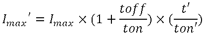
최대 휘도 신호(MI)에 의해 결정된 최대 휘도가 제2 영역(Second region)에 포함되는 경우, 비발광 기간에 대한 정보를 포함하는 발광 제어 타이밍 제어 신호(ECS)가 생성되면서 최대 휘도가 변경된다. 이 때 변경된 최대 휘도는 아래의 수학식에 의해 결정된다.
When the maximum luminance determined by the maximum luminance signal MI is included in the second region, the maximum luminance is changed while generating the emission control timing control signal ECS including information on the non-emission period. The maximum luminance changed at this time is determined by the following equation.

(Imax: 최대 휘도, Imax’; 변경된 최대 휘도, toff: 비발광 기간의 길이, ton: 발광 기간의 길이) (Imax: maximum luminance, Imax '; maximum luminance changed, toff: length of non-emission period, ton: length of emission period)
예를 들어, ton : toff = 0.8 : 0.2인 경우, 변경된 최대 휘도 Imax’는 최대 휘도 Imax의 1.25 배가 된다. 최대 휘도(Imax)로 한 프레임(1 Frame)동안 발광하는 경우의 한 프레임 동안의 평균 휘도는 Imax이고, 변경된 최대 휘도(1.25 Imax)로 한 프레임의 0.8배(0.8 Frame) 동안 발광하는 경우의 한 프레임 동안의 평균 휘도도 Imax이다. 따라서 수학식 2에 의해 최대 휘도가 변경되더라도 각각의 화소의 평균 휘도는 변경되지 않는다.
For example, when ton: toff = 0.8: 0.2, the changed maximum luminance Imax 'is 1.25 times the maximum luminance Imax. The average luminance during one frame in the case of emitting light for one frame at the maximum luminance Imax is Imax and the average luminance for one frame when the light is emitted for 0.8 times (frame) of one frame at the changed maximum luminance (1.25 Imax) The average luminance during the frame is also Imax. Therefore, even if the maximum luminance is changed by the equation (2), the average luminance of each pixel is not changed.
도 5는 도 1의 유기전계발광 표시장치의 최대 휘도가 제3 영역에 포함되는 경우 화소들을 발광시키는 방법을 설명하기 위한 도면이다. 설명의 편의를 위해, 화소들(P) 중 화소들(P(0, 0) 내지 P(6, 7)) 및 화소들(P(0, 0) 내지 P(6, 7))에 대해서만 설명될 것이다.FIG. 5 is a view for explaining a method of emitting light when the maximum luminance of the organic light emitting display device of FIG. 1 is included in the third region. Only the pixels P (0,0) to P (6,7) and the pixels P (0,0) to P (6,7) in the pixels P are explained Will be.
도 5의 (a)는 최대 휘도(Imax)가 150 nit이고 영상 신호들(RGB)이 변환되지 않아 모든 화소들(P)이 발광하는 경우를 설명하기 위한 도면이다. 화소들(P(0, 0) 내지 P(6, 7))에 대응하는 계조들은 화이트(white) 계조이며, 2 프레임 이상 동일하게 유지된다고 가정한다.5A is a diagram for explaining a case where all pixels P emit light because the maximum luminance Imax is 150 nit and the video signals RGB are not converted. It is assumed that the gradations corresponding to the pixels P (0, 0) to P (6, 7) are white gradations and remain the same for two or more frames.
도 5의 (b)는 제1 프레임에서 화소들(P(0, 0) 내지 P(6, 7))이 실제로 표시하는 화면을 설명하기 위한 도면이다. 유기전계발광 표시장치의 구동 주파수가 60 헤르쯔(Hz)인 경우, 제1 프레임은 1/60 초(sec) 동안 표시된다.FIG. 5B is a diagram for explaining a screen that the pixels P (0, 0) to P (6, 7) actually display in the first frame. When the driving frequency of the organic light emitting display device is 60 Hertz (Hz), the first frame is displayed for 1/60 second (sec).
제1 프레임(frame 1)에서, 화소(P(a, b))의 a+b가 짝수인 경우, 화소(P(a, b))에 대응하는 영상 신호(RGB(a, b))가 블랙(black) 계조에 대응하도록 변환된다. 예를 들어, 화소(P(0, 0))는 a+b 값이 0고 0은 짝수이므로 영상 신호(RGB(0, 0))가 블랙(black) 계조에 대응하도록 변환된다. 화소(P(0, 0))와 제1 방향 또는 제2 방향으로 이웃한 화소(P(0, 1)) 및 화소(P(1, 0))는 a+b 값이 1이고 1은 홀수이므로 영상 신호(RGB(0, 1)) 및 영상 신호(RGB(1, 0))는 블랙(black) 계조에 대응하도록 변환되지 않는다. 다만, 변환된 최대 휘도(Imax’)가 최대 휘도(Imax)의 2배인 300 nit가 된다.In the first frame (frame 1), when a + b of the pixel P (a, b) is an even number, the video signal RGB (a, b) corresponding to the pixel P And is converted to correspond to black gradation. For example, the pixel P (0, 0) is converted so that the video signal RGB (0, 0) corresponds to the black gradation because the a + b value is 0 and the 0 is an even number. A + b value is 1 and 1 is an odd number (0, 1) and a pixel P (0, 0) neighboring the pixel P (0, 0) in the first direction or the second direction. The video signals RGB (0, 1) and the video signals RGB (1, 0) are not converted to correspond to the black gradation. However, the converted maximum luminance Imax 'becomes 300 nit which is twice the maximum luminance Imax.
도 5의 (c)는 제2 프레임에서 화소들(P(0, 0) 내지 P(6, 7))이 실제로 표시하는 화면을 설명하기 위한 도면이다. 제1 프레임(frame 1) 직후, 제2 프레임(frame 2)이 표시된다고 가정할 수 있다. 제2 프레임(frame 2)에서, 화소(P(a, b))의 a+b가 홀수인 경우, 화소(P(a, b))에 대응하는 영상 신호(RGB(a, b))가 블랙(black) 계조에 대응하도록 변환된다. 예를 들어, 화소(P(0, 1)) 및 화소(P(1, 0))는 a+b 값이 1이고 1은 홀수이므로 영상 신호(RGB(0, 1)) 및 영상 신호(RGB(1, 0))가 블랙(black) 계조에 대응하도록 변환된다. 화소(P(0, 0))는 a+b 값이 0이고 0은 짝수이므로 영상 신호(RGB(0, 0))는 블랙(black) 계조에 대응하도록 변환되지 않는다. 다만, 변환된 최대 휘도(Imax’)가 최대 휘도(Imax)의 2배인 300 nit가 된다.FIG. 5C is a diagram for explaining a screen that the pixels P (0, 0) to P (6, 7) actually display in the second frame. Immediately after the first frame (frame 1), it can be assumed that the second frame (frame 2) is displayed. In the second frame (frame 2), when a + b of the pixel P (a, b) is an odd number, the video signal RGB (a, b) corresponding to the pixel P And is converted to correspond to black gradation. For example, since the pixel P (0, 1) and the pixel P (1, 0) have an a + b value of 1 and an odd number of 1, (1, 0)) is converted to correspond to the black gradation. The pixel (P (0, 0)) is not converted to correspond to the black gradation because the a + b value is 0 and the 0 is an even number. However, the converted maximum luminance Imax 'becomes 300 nit which is twice the maximum luminance Imax.
도 5의 (a)와 같이 2프레임동안 최대 휘도(Imax)가 150 nit인 경우와 도 5의 (b) 및 (c)와 같이 2프레임동안 변환된 최대 휘도(Imax’)가 300 nit인 경우가 비교될 것이다. 도 4의 (a)와 같이 2 프레임동안 최대 휘도(Imax)가 150 nit인 경우, 각각의 화소가 2 프레임동안 발광한 평균 휘도는 150 nit가 된다. 도 4의 (b) 및 (c)와 같이 2프레임동안 변환된 최대 휘도(Imax’)가 300 nit인 대신 화소들(P(0, 0) 내지 P(6, 7))이 2 프레임 중 1 프레임 동안만 발광하는 경우, 제1 프레임(frame 1) 및 제2 프레임(frame 2) 중 하나의 기간 동안 발광한 휘도는 300 nit이고 다른 하나의 기간 동안 발광한 휘도는 0nit이다. 따라서, 각각의 화소가 2 프레임동안 발광한 평균 휘도는 (300+0)/2 = 150 (nit)이 된다. 따라서, 도 5의 (a)와 같이 2프레임동안 최대 휘도(Imax)를 150 nit로 설정하는 경우와 도 5의 (b) 및 (c)와 같이 변환된 최대 휘도(Imax’)를 최대 휘도(Imax)의 2배로 설정하는 대신 화소들(P(0, 0) 내지 P(6, 7))이 2 프레임 중 1 프레임 동안만 발광하는 경우의 차이는 시청자들에게 인식되지 않는다.As shown in FIG. 5A, when the maximum luminance Imax is 150 nits for two frames and the maximum luminance Imax 'for two frames is 300 nits as shown in FIGS. 5B and 5C, Will be compared. As shown in FIG. 4A, when the maximum luminance Imax is 150 nits for two frames, the average luminance emitted by each pixel for two frames is 150 nits. The pixels P (0, 0) to P (6, 7) are replaced by pixels 1 (P (0, 0) to P (6, 7)) in which the maximum luminance Imax 'converted during two frames is 300 nit as shown in FIGS. When the light is emitted only during the frame, the luminance emitted for one period of the first frame (frame 1) and the second frame (frame 2) is 300 nit, and the luminance emitted for the other period is 0nit. Therefore, the average luminance emitted by each pixel for two frames becomes (300 + 0) / 2 = 150 (nit). Therefore, when the maximum luminance Imax is set to 150 nits for two frames and the converted maximum luminance Imax 'is set to the maximum luminance (Imax) as shown in (b) and (c) The difference in the case where the pixels P (0, 0) to P (6, 7) emit light for only one frame of two frames is not recognized by the viewers.
일반적으로, 변경된 최대 휘도는 아래의 수학식에 의해 결정된다.
In general, the changed maximum luminance is determined by the following equation.
(Imax: 최대 휘도, Imax’; 변경된 최대 휘도, t: 주기, ton: 주기 중 발광 기간의 길이) (Imax: maximum luminance, Imax '; maximum luminance changed, t: cycle, ton: length of light emission period in the cycle)
구체적으로, 도 5를 참조하여 설명된 실시예에서, 주기(t)는 2 프레임이고, 주기 중 발광 기간의 길이(ton)는 1 프레임이다. 따라서, 변경된 최대 휘도(Imax’)가 최대 휘도(Imax)의 2배가 되는 경우 최대 휘도가 변경되더라도 각각의 화소의 평균 휘도는 변경되지 않는다.Specifically, in the embodiment described with reference to FIG. 5, the period t is two frames, and the length of the light emission period in the period is one frame. Therefore, when the changed maximum luminance Imax 'is twice the maximum luminance Imax, the average luminance of each pixel is not changed even if the maximum luminance is changed.
영상 신호들(RGB)이 변환된 영상 신호들(RGBt)로 변환되고 비발광 기간에 대한 정보를 포함하는 발광 제어 타이밍 제어 신호(ECS)가 생성되는 경우, 최대 휘도는 아래의 수학식에 의해 변경된다.
When the image signals RGB are converted into the converted image signals RGBt and an emission control timing control signal ECS including information on the non-emission period is generated, the maximum luminance is changed by the following equation do.
(Imax: 최대 휘도, Imax’; 변경된 최대 휘도, toff: 한 프레임 내 비발광 기간의 길이, ton: 한 프레임 내 발광 기간의 길이, t’: 주기, ton’: 주기 중 발광 기간의 길이)
Emitting period in one frame, ton: length of light-emitting period in one frame, t ': period, ton': length of light-emitting period in the period)
도 6는 본 발명의 일 실시예에 따른 유기전계발광 표시장치의 구동 방법을 설명하기 위한 도면이다. 도 6을 참조로 설명되는 유기전계발광 표시장치의 구동 방법은 최대 휘도(Imax)가 제3 영역(Third region)에 해당되는 경우 비발광 기간에 대한 정보를 포함하지 않는 발광 제어 타이밍 제어 신호를 생성한다. 이하에서, 도 1 내지 도 6을 참조로 설명될 것이다.6 is a view for explaining a driving method of an organic light emitting display according to an embodiment of the present invention. The driving method of the organic light emitting display device described with reference to FIG. 6 generates an emission control timing control signal that does not include information on a non-emission period when the maximum luminance Imax corresponds to a third region do. Hereinafter, description will be made with reference to Figs. 1 to 6. Fig.
S1100 단계에서, 타이밍 컨트롤러(220)가 영상 신호들(RGB) 및 타이밍 신호들(Timing signals)을 수신한다. 일반적인 표시 장치에서 수행되는 단계이므로, 상세한 설명은 생략되어도 무방하다.In step S1100, the
S1200 단계에서, 타이밍 컨트롤러(220)가 최대 휘도 신호(MI)를 수신하고, 최대 휘도 신호(MI)를 기반으로 최대 휘도(Imax)를 결정한다. 도 6에서는 S1100 단계 이후 S1200 단계가 수행되었으나, 이는 실시예에 불과하다. S1200 단계 이후 S1100 단계가 수행될 수도 있고, S1100 단계 및 S1200 단계가 동시에 수행될 수도 있다.In step S1200, the
S1300 단계에서, 최대 휘도(Imax)가 제2 기준 최대 휘도(Imaxref2)와 비교된다. 최대 휘도(Imax)가 제2 기준 최대 휘도(Imaxref2)보다 높은 경우, S1400 단계가 수행된다. 그렇지 않은 경우, S1500 단계가 수행된다.In step S1300, the maximum luminance Imax is compared with the second reference maximum luminance Imaxref2. If the maximum luminance Imax is higher than the second reference maximum luminance Imaxref2, step S1400 is performed. Otherwise, step S1500 is performed.
S1400 단계에서, 최대 휘도(Imax)가 제2 기준 최대 휘도(Imaxref2)보다 높으므로, 타이밍 컨트롤러(220)가 영상 신호들(RGB)을 변경하지 않고, 비발광 기간에 대한 정보를 포함하지 않는 발광 제어 타이밍 제어 신호(ECS)를 생성한다. Since the maximum luminance Imax is higher than the second reference maximum luminance Imaxref2 in step S1400, the
S1500 단계에서, 최대 휘도(Imax)가 제1 기준 최대 휘도(Imaxref1)와 비교된다. 최대 휘도(Imax)가 제1 기준 최대 휘도(Imaxref1)보다 낮은 경우, S1600 단계가 수행된다. 그렇지 않은 경우, S1700 단계가 수행된다.In step S1500, the maximum luminance Imax is compared with the first reference maximum luminance Imaxref1. If the maximum luminance Imax is lower than the first reference maximum luminance Imaxref1, the step S1600 is performed. Otherwise, step S1700 is performed.
S1600 단계에서, 최대 휘도(Imax)가 제1 기준 최대 휘도(Imaxref1)보다 낮으므로, 타이밍 컨트롤러(220)가 영상 신호들(RGB)을 변환한다. S1600 단계에 의해, 변환된 영상 신호들(RGBt)이 생성된다. 또한, 최대 휘도(Imax)가 제2 영역(Second region)에 포함되지 않으므로, 타이밍 컨트롤러(220)가 비발광 기간에 대한 정보를 포함하지 않는 발광 제어 타이밍 제어 신호(ECS)를 생성한다.In step S1600, since the maximum luminance Imax is lower than the first reference maximum luminance Imaxref1, the
S1700 단계에서, 타이밍 컨트롤러(220)가 비발광 기간에 대한 정보를 포함하는 발광 제어 타이밍 제어 신호(ECS)를 생성한다.In step S1700, the
S1800 단계에서, 최대 휘도(Imax)가 변경된다. 최대 휘도(Imax)가 제2 영역(Second region)에 포함되는 경우 수학식 2를 기반으로 변경된 최대 휘도(Imax’)가 결정되고, 최대 휘도(Imax)가 제3 영역(Third region)에 포함되는 경우 수학식 3을 기반으로 변경된 최대 휘도(Imax’)가 결정된다.In step S1800, the maximum luminance Imax is changed. When the maximum luminance Imax is included in the second region, the changed maximum luminance Imax 'is determined based on Equation (2), and the maximum luminance Imax is included in the third region The changed maximum luminance Imax 'is determined based on Equation (3).
S1900 단계에서, 최대 휘도 룩업 테이블(231)이 호출되고, 최대 휘도(Imax)가 제1 영역(First region)에 포함되는 경우 최대 휘도(Imax)가 입력되며 최대 휘도(Imax)가 제2 영역(Second region) 또는 제3 영역(Third region)에 포함되는 경우 변경된 최대 휘도(Imax’)가 입력된다. 이후, 영상 신호들(RGB)에 대응하는 계조가 입력되는 경우, 최대 휘도 룩업 테이블(231)은 입력된 계조에 대응하는 데이터 전압 레벨을 출력한다.In step S1900, the maximum luminance Imax is inputted when the maximum luminance Imax is included in the first region and the maximum luminance Imax is inputted into the second region Second region) or a third region (Third region), the changed maximum luminance Imax 'is input. Then, when a gray level corresponding to the video signals RGB is inputted, the maximum brightness look-up table 231 outputs a data voltage level corresponding to the input gray level.
S2000 단계에서, 화소들(P)이 발광한다. 최대 휘도(Imax)가 제1 영역(First region)에 포함되는 경우, 최대 휘도(Imax), 비발광 기간에 대한 정보를 포함하지 않는 발광 제어 타이밍 제어 신호(ECS) 및 영상 신호들(RGB)을 기반으로 화소들(P)이 발광한다. 최대 휘도(Imax)가 제2 영역(Second region)에 포함되는 경우, 변경된 최대 휘도(Imax’), 비발광 기간에 대한 정보를 포함하는 발광 제어 타이밍 제어 신호(ECS) 및 영상 신호들(RGB)을 기반으로 화소들(P)이 발광한다. 최대 휘도(Imax)가 제3 영역(Third region)에 포함되는 경우, 변경된 최대 휘도(Imax’), 비발광 기간에 대한 정보를 포함하지 않는 발광 제어 타이밍 제어 신호(ECS) 및 변환된 영상 신호들(RGBt)를 기반으로 화소들(P)이 발광한다.
In step S2000, the pixels P emit light. When the maximum luminance Imax is included in the first region, the maximum luminance Imax, the emission control timing control signal ECS not including information on the non-emission period, and the video signals RGB The pixels P emit light. The emission control timing control signal ECS and the video signals RGB including information on the changed maximum luminance Imax 'and non-emission period, when the maximum luminance Imax is included in the second region, The pixels P emit light. When the maximum luminance Imax is included in the third region, the maximum luminance Imax 'changed, the emission control timing control signal ECS not including information on the non-emission period, The pixels P emit light on the basis of the RGBt.
도 7는 본 발명의 다른 실시예에 따른 유기전계발광 표시장치의 구동 방법을 설명하기 위한 도면이다. 도 7을 참조로 설명되는 유기전계발광 표시장치의 구동 방법은 최대 휘도(Imax)가 제3 영역(Third region)에 해당되는 경우 비발광 기간에 대한 정보를 포함하는 발광 제어 타이밍 제어 신호를 생성한다. 이하에서, 도 1 내지 도 7을 참조로 설명될 것이다.7 is a view for explaining a driving method of an organic light emitting display according to another embodiment of the present invention. The driving method of the organic light emitting display device described with reference to FIG. 7 generates an emission control timing control signal including information on a non-emission period when the maximum luminance Imax corresponds to a third region . Hereinafter, description will be made with reference to Figs. 1 to 7.
S1100’ 단계, S1200’ 단계, S1300’ 단계, S1400’ 단계, S1500’ 단계 및 S1900’ 단계는 각각 S1100 단계, S1200 단계, S1300 단계, S1400 단계, S1500 단계 및 S1900 단계와 동일하므로 상세한 설명이 생략되어도 무방하다.Steps S1100 ', S1200', S1300 ', S1400', S1500 'and S1900' are the same as S1100, S1200, S1300, S1400, S1500 and S1900, respectively, It is acceptable.
S1600’ 단계에서, 최대 휘도(Imax)가 제1 기준 최대 휘도(Imaxref1)보다 낮으므로, 타이밍 컨트롤러(220)가 영상 신호들(RGB)을 변환한다. S1500 단계에 의해, 변환된 영상 신호들(RGBt)이 생성된다. S1600’ 단계 이후, S1700’ 단계가 수행된다.Since the maximum luminance Imax is lower than the first reference maximum luminance Imaxref1 in step S1600 ', the
S1700’ 단계에서, 타이밍 컨트롤러(220)가 비발광 기간에 대한 정보를 포함하는 발광 제어 타이밍 제어 신호(ECS)를 생성한다. 최대 휘도(Imax)가 제2 기준 최대 휘도(Imaxref2)보다 낮은 경우에는 비발광 기간에 대한 정보를 포함하지 않는 발광 제어 타이밍 제어 신호(ECS)를 생성한다. 즉, 최대 휘도(Imax)가 제2 영역(Second region) 또는 제3 영역(Third region)에 포함되는 경우, 타이밍 컨트롤러(220)가 비발광 기간에 대한 정보를 포함하는 발광 제어 타이밍 제어 신호(ECS)를 생성한다.In step S1700 ', the
S1800’ 단계에서, 최대 휘도(Imax)가 변경된다. 최대 휘도(Imax)가 제2 영역(Second region)에 포함되는 경우 수학식 2를 기반으로 변경된 최대 휘도(Imax’)가 결정되고, 최대 휘도(Imax)가 제3 영역(Third region)에 포함되는 경우 수학식 4를 기반으로 변경된 최대 휘도(Imax’)가 결정된다.In step S1800 ', the maximum luminance Imax is changed. When the maximum luminance Imax is included in the second region, the changed maximum luminance Imax 'is determined based on Equation (2), and the maximum luminance Imax is included in the third region The changed maximum luminance Imax 'is determined based on Equation (4).
S2000’ 단계에서, 화소들(P)이 발광한다. 최대 휘도(Imax)가 제1 영역(First region)에 포함되는 경우, 최대 휘도(Imax), 비발광 기간에 대한 정보를 포함하지 않는 발광 제어 타이밍 제어 신호(ECS) 및 영상 신호들(RGB)을 기반으로 화소들(P)이 발광한다. 최대 휘도(Imax)가 제2 영역(Second region)에 포함되는 경우, 변경된 최대 휘도(Imax’), 비발광 기간에 대한 정보를 포함하는 발광 제어 타이밍 제어 신호(ECS) 및 영상 신호들(RGB)을 기반으로 화소들(P)이 발광한다. 최대 휘도(Imax)가 제3 영역(Third region)에 포함되는 경우, 변경된 최대 휘도(Imax’), 비발광 기간에 대한 정보를 포함하는 발광 제어 타이밍 제어 신호(ECS) 및 변환된 영상 신호들(RGBt)를 기반으로 화소들(P)이 발광한다.
In step S2000 ', the pixels P emit light. When the maximum luminance Imax is included in the first region, the maximum luminance Imax, the emission control timing control signal ECS not including information on the non-emission period, and the video signals RGB The pixels P emit light. The emission control timing control signal ECS and the video signals RGB including information on the changed maximum luminance Imax 'and non-emission period, when the maximum luminance Imax is included in the second region, The pixels P emit light. When the maximum luminance Imax is included in the third region, the emission control timing control signal ECS including information on the changed maximum luminance Imax ', the non-emission period, and the converted video signals ( RGBt), the pixels P emit light.
도 8은 도 6의 유기전계발광 표시장치의 구동 방법 중 영상 신호들을 변환하는 단계를 설명하기 위한 도면이다.8 is a view for explaining a step of converting image signals in the driving method of the organic light emitting display of FIG.
S1610 단계에서, 디스플레이 패널 내 각각의 화소의 위치를 기반으로 변경 필요 화소 정보가 생성된다. 예를 들어 제1 프레임(frame 1)에서 화소(P(a, b))의 a+b가 짝수인 경우, 화소(P(a, b))는 타이밍 컨트롤러(220)에 의해 생성되는 변경 필요 화소 정보에 포함된다.In step S1610, change necessary pixel information is generated based on the position of each pixel in the display panel. For example, when a + b of the pixel P (a, b) in the first frame (frame 1) is an even number, the pixel P (a, b) Is included in the pixel information.
S1620 단계에서, 변경 필요 화소 정보에 대응하는 영상 신호들이 블랙(black) 계조에 대응하도록 변환된다. 예를 들어 제1 프레임(frame 1)에서, a+b가 짝수인 화소(P(a, b))에 대응하는 영상 신호(RGB(a, b))는 블랙 계조에 대응하도록 변환된다. S1620 단계에 의해 변환된 영상 신호들(RGBt)이 생성된다.
In step S1620, the video signals corresponding to the change-necessary pixel information are converted so as to correspond to the black gradation. For example, in the first frame (frame 1), the image signals RGB (a, b) corresponding to the pixels P (a, b) having an even number of a + b are converted so as to correspond to black gradations. The video signals RGBt converted in step S1620 are generated.
도 9는 도 6의 유기전계발광 표시장치의 구동 방법 중 비발광 기간에 대한 정보를 포함하는 발광 제어 타이밍 제어 신호를 생성하는 단계를 설명하기 위한 도면이다.9 is a view for explaining a step of generating an emission control timing control signal including information on a non-emission period in the driving method of the organic light emitting display of FIG.
S1710 단계에서, 비발광 기간(Toff)의 길이가 결정된다. 비발광 기간(Toff)은 최대 휘도(Imax) 등을 기반으로 결정될 수 있다.In step S1710, the length of the non-emission period Toff is determined. The non-emission period Toff can be determined based on the maximum luminance Imax and the like.
S1720 단계에서, 타이밍 컨트롤러(220)가 결정된 비발광 길이를 기반으로 발광 제어 타이밍 제어 신호(ECS)를 생성한다.
In step S1720, the
이상 설명한 내용을 통해 당업자라면 본 발명의 기술사상을 일탈하지 아니하는 범위에서 다양한 변경 및 수정이 가능함을 알 수 있을 것이다. 따라서, 본 발명의 기술적 범위는 명세서의 상세한 설명에 기재된 내용으로 한정되는 것이 아니라 특허 청구의 범위에 의해 정하여져야만 할 것이다.It will be apparent to those skilled in the art that various modifications and variations can be made in the present invention without departing from the spirit or scope of the invention. Therefore, the technical scope of the present invention should not be limited to the contents described in the detailed description of the specification, but should be defined by the claims.
100: 디스플레이 패널
220: 타이밍 컨트롤러
221: 기준 계조 룩업 테이블
100: display panel 220: timing controller
221: Reference grayscale look-up table
Claims (19)
상기 디스플레이 패널 구동부는 최대 휘도 신호를 수신하며,
상기 최대 휘도 신호를 기반으로 결정된 최대 휘도가 제1 기준 최대 휘도보다 낮은 경우 한 프레임 내에서 상기 화소들 중 일부 화소들만 발광시키고,
상기 최대 휘도가 상기 제1 기준 최대 휘도보다 높고 제2 기준 최대 휘도보다 낮은 경우 상기 화소들이 한 프레임 중 일부 기간에 발광하지 않으며,
상기 제2 기준 최대 휘도는 상기 제1 기준 최대 휘도보다 높은 유기전계발광 표시장치.A display panel including pixels, and a display panel driver for driving the display panel,
The display panel driver receives the maximum luminance signal,
When a maximum luminance determined based on the maximum luminance signal is lower than a first reference maximum luminance, only some of the pixels are emitted within one frame,
When the maximum luminance is higher than the first reference maximum luminance and lower than the second reference maximum luminance, the pixels do not emit light in a part of one frame,
And the second reference maximum luminance is higher than the first reference maximum luminance.
상기 디스플레이 패널 구동부는,
입력된 최대 휘도 및 계조를 기반으로 데이터 전압 레벨을 출력하는 최대 휘도 룩업 테이블을 더 포함하고,
상기 최대 휘도가 상기 제2 기준 최대 휘도보다 높은 경우 상기 최대 휘도가 상기 최대 휘도 룩업 테이블에 입력되며,
상기 최대 휘도가 상기 제2 기준 최대 휘도보다 낮은 경우, 상기 디스플레이 패널 구동부는 상기 최대 휘도를 상기 제2 기준 최대 휘도보다 높은 값으로 변환하고, 변환된 최대 휘도가 상기 최대 휘도 룩업 테이블에 입력되는 유기전계발광 표시장치.The method according to claim 1,
The display panel driver may include:
Further comprising a maximum luminance lookup table for outputting a data voltage level based on the inputted maximum luminance and gradation,
When the maximum luminance is higher than the second reference maximum luminance, the maximum luminance is input to the maximum luminance lookup table,
Wherein the display panel driver converts the maximum luminance to a value higher than the second reference maximum luminance when the maximum luminance is lower than the second reference maximum luminance, An electroluminescent display device.
상기 최대 휘도 룩업 테이블은 상기 타이밍 컨트롤러 또는 상기 데이터 구동부에 포함되는 유기전계발광 표시장치.3. The method of claim 2,
Wherein the maximum luminance lookup table is included in the timing controller or the data driver.
상기 디스플레이 패널 구동부는,
영상 신호들, 타이밍 신호들 및 상기 최대 휘도 신호를 수신하고 스캔 타이밍 제어 신호 및 데이터 타이밍 제어 신호를 공급하는 타이밍 컨트롤러를 포함하고,
상기 타이밍 컨트롤러는 변환 여부 신호를 생성하는 변환 여부 신호 생성부 및 상기 변환 여부 신호를 수신하는 영상 신호 변환부를 포함하며,
상기 최대 휘도가 상기 제1 기준 최대 휘도보다 낮은 경우, 상기 변환 여부 신호 생성부는 상기 제1 논리 값을 가지는 변환 여부 신호를 생성하고, 상기 영상 신호 변환부는 상기 영상 신호들을 변환하며, 상기 타이밍 컨트롤러는 변환된 영상 신호들을 출력하고,
상기 최대 휘도가 상기 제1 기준 최대 휘도보다 높은 경우, 상기 변환 여부 신호 생성부는 상기 제1 논리 값과 다른 제2 논리 값을 가지는 변환 여부 신호를 생성하고, 상기 타이밍 컨트롤러는 상기 영상 신호를 출력하는 유기전계발광 표시장치.The method according to claim 1,
The display panel driver may include:
And a timing controller for receiving the video signals, the timing signals and the maximum luminance signal, and supplying a scan timing control signal and a data timing control signal,
Wherein the timing controller includes a conversion signal generator for generating a conversion signal, and a video signal converter for receiving the conversion signal,
Wherein the conversion enable signal generator generates a conversion enable signal having the first logic value when the maximum brightness is lower than the first reference maximum brightness and the video signal converter converts the video signals, Outputs the converted video signals,
Wherein the conversion request signal generator generates a conversion request signal having a second logic value different from the first logic value when the maximum luminance is higher than the first reference maximum luminance and the timing controller outputs the conversion signal Organic electroluminescence display device.
상기 영상 신호 변환부는 한 프레임에 대응하는 영상 신호의 변경이 필요한 화소 정보를 저장하고,
상기 최대 휘도가 상기 제1 기준 최대 휘도보다 낮은 경우, 상기 영상 신호 변환부가 상기 화소 정보에 대응하는 영상 신호들을 블랙(black) 계조에 대응하도록 변환하는 것에 의해 상기 변환된 영상 신호들이 생성되는 유기전계발광 표시장치.5. The method of claim 4,
Wherein the image signal conversion unit stores pixel information that needs to be changed in a video signal corresponding to one frame,
Wherein when the maximum luminance is lower than the first reference maximum luminance, the image signal converting unit converts the image signals corresponding to the pixel information to correspond to a black gradation, Emitting display device.
상기 최대 휘도가 상기 제1 기준 최대 휘도보다 낮은 경우, 상기 타이밍 컨트롤러는 상기 최대 휘도를 상기 제2 기준 최대 휘도보다 높은 값으로 변경하고,
상기 최대 휘도를 기반으로 상기 영상 신호들이 표시되는 경우의 각각의 화소의 평균 휘도는 변경된 최대 휘도를 기반으로 상기 변환된 영상 신호들이 표시되는 경우의 각각의 화소의 평균 휘도에 대응하는 유기전계발광 표시장치.6. The method of claim 5,
When the maximum brightness is lower than the first reference maximum brightness, the timing controller changes the maximum brightness to a value higher than the second reference maximum brightness,
The average luminance of each pixel in the case where the video signals are displayed based on the maximum luminance is determined based on the maximum luminance of the organic light emitting display corresponding to the average luminance of each pixel when the converted video signals are displayed based on the changed maximum luminance. Device.
상기 디스플레이 패널은 상기 화소들에 데이터 전압들을 전달하는 데이터 라인들, 상기 화소들에 스캔 신호들을 전달하는 스캔 라인들 및 상기 화소들에 발광 제어 신호들을 전달하는 발광 제어 라인들을 포함하고,
상기 디스플레이 패널 구동부는,
발광 제어 타이밍 제어 신호를 더 공급하고,
상기 영상 신호들 또는 상기 변환된 영상 신호들을 기반으로 상기 데이터 전압들을 생성하고, 상기 스캔 타이밍 제어 신호가 공급되는 타이밍을 기반으로 상기 데이터 전압들을 상기 데이터 라인들에 공급하는 데이터 구동부;
상기 스캔 타이밍 제어 신호가 공급되는 타이밍을 기반으로 상기 스캔 신호들을 상기 스캔 라인들에 공급하는 스캔 구동부; 및
상기 발광 제어 타이밍 제어 신호가 공급되는 타이밍을 기반으로 상기 발광 제어 신호들을 공급하는 발광 제어 구동부를 더 포함하는 유기전계발광 표시장치. 5. The method of claim 4,
Wherein the display panel includes data lines for transmitting data voltages to the pixels, scan lines for transmitting scan signals to the pixels, and emission control lines for transmitting emission control signals to the pixels,
The display panel driver may include:
The light emission control timing control signal is further supplied,
A data driver for generating the data voltages based on the image signals or the converted image signals and supplying the data voltages to the data lines based on a timing at which the scan timing control signal is supplied;
A scan driver for supplying the scan signals to the scan lines based on a timing at which the scan timing control signal is supplied; And
And a light emission control driver for supplying the light emission control signals based on a timing at which the light emission control timing control signal is supplied.
상기 최대 휘도가 상기 제1 기준 최대 휘도보다 높고 상기 제2 기준 최대 휘도보다 낮은 경우 상기 발광 제어 타이밍 제어 신호는 비발광 기간에 대한 정보를 포함하고,
상기 최대 휘도가 상기 제2 기준 최대 휘도보다 높은 경우 상기 발광 제어 타이밍 제어 신호는 비발광 기간에 대한 정보를 포함하지 않는 유기전계발광 표시장치.8. The method of claim 7,
Wherein the emission control timing control signal includes information on a non-emission period when the maximum luminance is higher than the first reference maximum luminance and lower than the second reference maximum luminance,
And the emission control timing control signal does not include information on a non-emission period when the maximum luminance is higher than the second reference maximum luminance.
상기 최대 휘도가 상기 제1 기준 최대 휘도보다 높고 상기 제2 기준 최대 휘도보다 낮은 경우, 상기 타이밍 컨트롤러는 상기 최대 휘도를 상기 제2 기준 최대 휘도보다 높은 값으로 변경하고,
상기 최대 휘도 및 상기 비발광 기간에 대한 정보를 포함하지 않는 발광 제어 타이밍 제어 신호를 기반으로 상기 영상 신호들이 표시되는 경우의 각각의 화소의 평균 휘도는 변경된 최대 휘도 및 상기 비발광 기간에 대한 정보를 포함하는 발광 제어 타이밍 제어 신호를 기반으로 상기 영상 신호들이 표시되는 경우의 각각의 화소의 평균 휘도에 대응하는 유기전계발광 표시장치.9. The method of claim 8,
When the maximum luminance is higher than the first reference maximum luminance and lower than the second reference maximum luminance, the timing controller changes the maximum luminance to a value higher than the second reference maximum luminance,
The average luminance of each pixel in the case where the video signals are displayed based on the emission control timing control signal which does not include the maximum luminance and the information on the non-emission period is calculated by using the changed maximum luminance and information on the non- And the light emission control timing control signal includes a light emission control timing control signal corresponding to an average brightness of each pixel when the image signals are displayed.
최대 휘도가 상기 제2 기준 최대 휘도보다 낮은 경우에도 상기 화소들이 한 프레임 중 일부 기간에 발광하지 않는 유기전계발광 표시장치.The method according to claim 1,
The pixels do not emit light in a part of one frame even when the maximum luminance is lower than the second reference maximum luminance.
영상 신호들 및 타이밍 신호들을 수신하는 단계;
최대 휘도 신호를 수신하여 최대 휘도를 결정하는 단계;
영상 신호들을 변환하는 단계;
비발광 기간에 대한 정보를 포함하는 발광 제어 타이밍 제어 신호를 생성하는 단계;
룩업 테이블(Look-up Table)을 호출하는 단계; 및
상기 화소들을 발광시키는 단계를 포함하고,
상기 영상 신호들을 변환하는 단계는 상기 최대 휘도가 상기 제1 기준 최대 휘도보다 낮은 경우에 수행되며,
상기 비발광 기간에 대한 정보를 포함하는 발광 제어 타이밍 제어 신호를 생성하는 단계는 상기 최대 휘도가 상기 제1 기준 최대 휘도보다 높고 제2 기준 최대 휘도보다 낮은 경우에 수행되고,
상기 제2 기준 최대 휘도는 상기 제1 기준 최대 휘도보다 높은 유기전계발광 표시장치의 구동 방법.A method of driving an organic light emitting display including a display panel including pixels and a display panel driver driving the display panel,
Receiving video signals and timing signals;
Receiving a maximum luminance signal and determining a maximum luminance;
Converting the video signals;
Generating an emission control timing control signal including information on a non-emission period;
Calling a look-up table; And
And causing the pixels to emit light,
Wherein the converting of the image signals is performed when the maximum luminance is lower than the first reference maximum luminance,
Wherein the step of generating an emission control timing control signal including information on the non-emission period is performed when the maximum luminance is higher than the first reference maximum luminance and lower than the second reference maximum luminance,
And the second reference maximum luminance is higher than the first reference maximum luminance.
상기 영상 신호들을 변환하는 단계 이후에도 상기 비발광 기간에 대한 정보를 포함하는 발광 제어 타이밍 제어 신호를 생성하는 단계가 수행되는 유기전계발광 표시장치의 구동 방법.12. The method of claim 11,
Wherein the step of generating an emission control timing control signal including information on the non-emission period is performed after the step of converting the video signals.
상기 영상 신호들을 변환하는 단계에서, 상기 비발광 기간에 대한 정보를 포함하지 않는 발광 제어 타이밍 제어 신호가 생성되는 유기전계발광 표시장치의 구동 방법.12. The method of claim 11,
And generating an emission control timing control signal that does not include information on the non-emission period in the step of converting the video signals.
상기 유기전계발광 표시장치의 구동 방법은 상기 최대 휘도를 변경하는 단계를 더 포함하고,
상기 최대 휘도를 변경하는 단계는 상기 영상 신호들을 변환하는 단계 또는 상기 비발광 기간에 대한 정보를 포함하는 발광 제어 타이밍 제어 신호를 생성하는 단계 이후에 수행되고, 상기 룩업 테이블을 호출하는 단계 이전에 수행되는 유기전계발광 표시장치의 구동 방법.12. The method of claim 11,
The driving method of the organic light emitting display further includes changing the maximum luminance,
The step of changing the maximum luminance may be performed after the step of converting the video signals or generating the light emission control timing control signal including information on the non-light emission period, and before the step of calling the lookup table And a driving method of the organic light emitting display device.
상기 영상 신호들을 변환하는 단계는,
디스플레이 패널 내 각각의 화소의 위치를 기반으로 변경 필요 화소 정보를 생성하는 단계; 및
상기 변경 필요 화소 정보에 대응하는 영상 신호들을 블랙(black) 계조에 대응하도록 변환하는 단계를 포함하는 유기전계발광 표시장치의 구동 방법.15. The method of claim 14,
Wherein the converting the video signals comprises:
Generating changing pixel information based on the position of each pixel in the display panel; And
And converting the video signals corresponding to the change-requiring pixel information to correspond to black gradation.
상기 최대 휘도를 변경하는 단계에서 변경된 최대 휘도가 생성되고,
상기 최대 휘도를 기반으로 상기 영상 신호들이 표시되는 경우의 각각의 화소의 평균 휘도가 상기 변경된 최대 휘도를 기반으로 변환된 영상 신호들이 표시되는 경우의 각각의 화소의 평균 휘도에 대응하도록 상기 변경된 최대 휘도의 레벨이 설정되는 유기전계발광 표시장치의 구동 방법.16. The method of claim 15,
The changed maximum luminance is generated in the step of changing the maximum luminance,
And changing the average brightness of each pixel when the image signals are displayed based on the maximum brightness so as to correspond to the average brightness of each pixel when the image signals converted based on the changed maximum brightness are displayed, Is set to the level of the organic electroluminescent display device.
상기 비발광 기간에 대한 정보를 포함하는 발광 제어 타이밍 제어 신호를 생성하는 단계는,
비발광 기간의 길이를 결정하는 단계; 및
결정된 비발광 기간의 길이를 기반으로 상기 발광 제어 타이밍 제어 신호를 생성하는 단계를 포함하는 유기전계발광 표시장치의 구동 방법.15. The method of claim 14,
Wherein the step of generating an emission control timing control signal including information on the non-emission period comprises:
Determining a length of the non-emission period; And
And generating the emission control timing control signal based on the determined length of the non-emission period.
상기 최대 휘도를 변경하는 단계에서 변경된 최대 휘도가 생성되고,
상기 최대 휘도 및 상기 비발광 기간에 대한 정보를 포함하지 않는 발광 제어 타이밍 제어 신호를 기반으로 영상 신호들이 표시되는 경우의 각각의 화소의 평균 휘도가 상기 변경된 최대 휘도 및 상기 비발광 기간에 대한 정보를 포함하는 발광 제어 타이밍 제어 신호를 기반으로 영상 신호들이 표시되는 경우의 각각의 화소의 평균 휘도에 대응하도록 상기 변경된 최대 휘도의 레벨이 설정되는 유기전계발광 표시장치의 구동 방법.18. The method of claim 17,
The changed maximum luminance is generated in the step of changing the maximum luminance,
The average brightness of each pixel in the case where the video signals are displayed based on the emission control timing control signal that does not include the maximum luminance and the information on the non-emission period is information on the changed maximum luminance and the non- And the level of the changed maximum luminance is set to correspond to the average luminance of each pixel in the case where image signals are displayed based on the emission control timing control signal.
상기 유기전계발광 표시장치의 구동 방법은 비발광 기간에 대한 정보를 포함하지 않는 발광 제어 타이밍 제어 신호를 생성하는 단계를 더 포함하고,
상기 비발광 기간에 대한 정보를 포함하지 않는 발광 제어 타이밍 제어 신호를 생성하는 단계는 상기 최대 휘도가 상기 제2 기준 최대 휘도보다 높은 경우에 수행되는 유기전계발광 표시장치의 구동 방법.
12. The method of claim 11,
The driving method of the organic light emitting display further includes generating an emission control timing control signal that does not include information on a non-emission period,
Wherein the step of generating an emission control timing control signal that does not include information on the non-emission period is performed when the maximum luminance is higher than the second reference maximum luminance.
Priority Applications (3)
| Application Number | Priority Date | Filing Date | Title |
|---|---|---|---|
| KR1020150095956A KR102473208B1 (en) | 2015-07-06 | 2015-07-06 | Organic light emitting display device and driving method thereof |
| US15/159,671 US10522075B2 (en) | 2015-07-06 | 2016-05-19 | Organic light emitting display device and method of driving the same |
| CN201610525649.4A CN106340267B (en) | 2015-07-06 | 2016-07-06 | Organic light emitting display device and method of driving the same |
Applications Claiming Priority (1)
| Application Number | Priority Date | Filing Date | Title |
|---|---|---|---|
| KR1020150095956A KR102473208B1 (en) | 2015-07-06 | 2015-07-06 | Organic light emitting display device and driving method thereof |
Publications (2)
| Publication Number | Publication Date |
|---|---|
| KR20170005941A true KR20170005941A (en) | 2017-01-17 |
| KR102473208B1 KR102473208B1 (en) | 2022-12-05 |
Family
ID=57731362
Family Applications (1)
| Application Number | Title | Priority Date | Filing Date |
|---|---|---|---|
| KR1020150095956A KR102473208B1 (en) | 2015-07-06 | 2015-07-06 | Organic light emitting display device and driving method thereof |
Country Status (3)
| Country | Link |
|---|---|
| US (1) | US10522075B2 (en) |
| KR (1) | KR102473208B1 (en) |
| CN (1) | CN106340267B (en) |
Cited By (1)
| Publication number | Priority date | Publication date | Assignee | Title |
|---|---|---|---|---|
| US11205373B2 (en) | 2019-04-22 | 2021-12-21 | Samsung Electronics Co., Ltd. | Display apparatus to mitigate dimming phenomenon and control method thereof |
Families Citing this family (11)
| Publication number | Priority date | Publication date | Assignee | Title |
|---|---|---|---|---|
| JP2018013696A (en) * | 2016-07-22 | 2018-01-25 | キヤノン株式会社 | Image processing apparatus and display apparatus |
| KR102537993B1 (en) | 2017-10-31 | 2023-06-01 | 삼성디스플레이 주식회사 | Method for setting black data of disply device and disply device employing the same |
| KR102498285B1 (en) | 2018-02-23 | 2023-02-10 | 삼성디스플레이 주식회사 | Display device and method of driving the same |
| KR102533763B1 (en) | 2018-03-27 | 2023-05-19 | 삼성디스플레이 주식회사 | Organic light emitting display device |
| KR102533624B1 (en) | 2018-04-24 | 2023-05-18 | 삼성디스플레이 주식회사 | Gamma correction device for a display device, gamma correction method for a display device, and display devcie |
| KR102485164B1 (en) | 2018-05-03 | 2023-01-09 | 삼성디스플레이 주식회사 | Driving voltage setting device, method of setting driving voltage for display device, and display device |
| CN208335702U (en) * | 2018-05-14 | 2019-01-04 | 北京京东方技术开发有限公司 | Display panel and display device |
| KR102532775B1 (en) | 2018-10-10 | 2023-05-17 | 삼성디스플레이 주식회사 | Display device |
| US11282432B2 (en) | 2019-02-28 | 2022-03-22 | Samsung Display Co., Ltd. | Display device and driving method thereof |
| KR20200113068A (en) | 2019-03-20 | 2020-10-06 | 삼성디스플레이 주식회사 | Luminance control unit and display device including the same |
| KR20210084765A (en) | 2019-12-27 | 2021-07-08 | 삼성디스플레이 주식회사 | Optical compensation system and optical compensation method of display devcie |
Citations (5)
| Publication number | Priority date | Publication date | Assignee | Title |
|---|---|---|---|---|
| KR20060122307A (en) * | 2005-05-26 | 2006-11-30 | 엘지전자 주식회사 | Oled |
| US20120098870A1 (en) * | 2010-10-25 | 2012-04-26 | Apple Inc. | Oled driving technique |
| US20130169693A1 (en) * | 2011-12-29 | 2013-07-04 | Si-Baek PYO | Method of compensating gamma reference voltages, and gamma reference voltage compensation circuit |
| KR20130136338A (en) * | 2012-06-04 | 2013-12-12 | 삼성전자주식회사 | Organic lighting emitting display and driving method thereof |
| KR20140058283A (en) * | 2012-11-06 | 2014-05-14 | 삼성디스플레이 주식회사 | Display device and method of driving thereof |
Family Cites Families (15)
| Publication number | Priority date | Publication date | Assignee | Title |
|---|---|---|---|---|
| KR20050032321A (en) * | 2003-10-01 | 2005-04-07 | 삼성에스디아이 주식회사 | Field emission display and deriving me thod thereof |
| JP4341839B2 (en) * | 2003-11-17 | 2009-10-14 | シャープ株式会社 | Image display device, electronic apparatus, liquid crystal television device, liquid crystal monitor device, image display method, display control program, and recording medium |
| JP4862369B2 (en) * | 2005-11-25 | 2012-01-25 | ソニー株式会社 | Self-luminous display device, peak luminance adjusting device, electronic device, peak luminance adjusting method and program |
| KR101362981B1 (en) * | 2007-01-05 | 2014-02-21 | 삼성디스플레이 주식회사 | Organic light emitting display device and driving method thereof |
| KR100844775B1 (en) * | 2007-02-23 | 2008-07-07 | 삼성에스디아이 주식회사 | Organic light emitting display device |
| BRPI0811055A2 (en) * | 2007-05-25 | 2015-01-27 | Sony Corp | DISPLAY DEVICE, METHOD OF PROCESSING AN IMAGE ISNAL TO A DISPLAY DEVICE, AND PROGRAM RELATED TO THE DISPLAY |
| JP5211732B2 (en) * | 2008-02-14 | 2013-06-12 | ソニー株式会社 | Lighting period setting method, display panel driving method, lighting condition setting device, semiconductor device, display panel, and electronic apparatus |
| KR101152464B1 (en) * | 2010-05-10 | 2012-06-01 | 삼성모바일디스플레이주식회사 | Organic Light Emitting Display Device and Driving Method Thereof |
| KR20130081451A (en) | 2012-01-09 | 2013-07-17 | 삼성디스플레이 주식회사 | Display device and driving method thereof |
| KR102000178B1 (en) | 2012-01-26 | 2019-07-17 | 삼성디스플레이 주식회사 | Organic Light Emitting Display Device and Driving Method Thereof |
| US10155121B2 (en) * | 2012-08-25 | 2018-12-18 | National Chiao Tung University | Stimuli generating methods, devices and control systems to induce visual evoked potentials using imperceptible flickering multi-color lights |
| KR102062776B1 (en) * | 2013-08-02 | 2020-01-07 | 삼성디스플레이 주식회사 | Display device and driving method thereof |
| KR102081408B1 (en) | 2013-10-04 | 2020-02-26 | 삼성디스플레이 주식회사 | dimming driving method for Organic Light Emitting Display Device |
| KR102074719B1 (en) * | 2013-10-08 | 2020-02-07 | 엘지디스플레이 주식회사 | Organic light emitting display device |
| KR102139693B1 (en) | 2013-11-18 | 2020-07-31 | 삼성디스플레이 주식회사 | Method of controlling luminance, luminance control unit, and organic light emitting display device having the same |
-
2015
- 2015-07-06 KR KR1020150095956A patent/KR102473208B1/en active IP Right Grant
-
2016
- 2016-05-19 US US15/159,671 patent/US10522075B2/en active Active
- 2016-07-06 CN CN201610525649.4A patent/CN106340267B/en active Active
Patent Citations (6)
| Publication number | Priority date | Publication date | Assignee | Title |
|---|---|---|---|---|
| KR20060122307A (en) * | 2005-05-26 | 2006-11-30 | 엘지전자 주식회사 | Oled |
| US20120098870A1 (en) * | 2010-10-25 | 2012-04-26 | Apple Inc. | Oled driving technique |
| US20130169693A1 (en) * | 2011-12-29 | 2013-07-04 | Si-Baek PYO | Method of compensating gamma reference voltages, and gamma reference voltage compensation circuit |
| KR20150010807A (en) * | 2011-12-29 | 2015-01-29 | 삼성디스플레이 주식회사 | Method and circuit for compensating gamma reference voltages |
| KR20130136338A (en) * | 2012-06-04 | 2013-12-12 | 삼성전자주식회사 | Organic lighting emitting display and driving method thereof |
| KR20140058283A (en) * | 2012-11-06 | 2014-05-14 | 삼성디스플레이 주식회사 | Display device and method of driving thereof |
Cited By (1)
| Publication number | Priority date | Publication date | Assignee | Title |
|---|---|---|---|---|
| US11205373B2 (en) | 2019-04-22 | 2021-12-21 | Samsung Electronics Co., Ltd. | Display apparatus to mitigate dimming phenomenon and control method thereof |
Also Published As
| Publication number | Publication date |
|---|---|
| US10522075B2 (en) | 2019-12-31 |
| KR102473208B1 (en) | 2022-12-05 |
| CN106340267B (en) | 2020-12-22 |
| US20170011682A1 (en) | 2017-01-12 |
| CN106340267A (en) | 2017-01-18 |
Similar Documents
| Publication | Publication Date | Title |
|---|---|---|
| KR102473208B1 (en) | Organic light emitting display device and driving method thereof | |
| KR102383741B1 (en) | Pixel, organic light emitting display device including the pixel and driving method of the pixel | |
| US10937370B2 (en) | Data driving circuit, display panel and display | |
| US9466243B2 (en) | Compensation of threshold voltage in driving transistor of organic light emitting diode display device | |
| KR102016614B1 (en) | Organic light emitting display device and method for driving the same | |
| KR101015339B1 (en) | Pixel and Organic Light Emitting Display Using The Pixel | |
| KR100986915B1 (en) | Organic Light Emitting Display and Driving Method Thereof | |
| KR101008482B1 (en) | Pixel and Organic Light Emitting Display Using The Pixel | |
| KR101056302B1 (en) | Organic light emitting display | |
| KR101155898B1 (en) | Organic light emitting display and driving method thereof | |
| KR101056247B1 (en) | Pixel and organic light emitting display device using same | |
| CN113053281B (en) | Pixel driving circuit and electroluminescent display device including the same | |
| KR102081993B1 (en) | Organic light emitting display device and method for driving the same | |
| KR20140134046A (en) | Organic Light Emitting Display Device and Driving Method Threrof | |
| KR20140058283A (en) | Display device and method of driving thereof | |
| JP6960026B2 (en) | Display device | |
| KR101469027B1 (en) | Display device and driving method thereof | |
| CN111883053A (en) | Display device and method of driving the same | |
| KR20170013485A (en) | Pixel, organic light emitting display device including the pixel and driving method of organic light emitting display device | |
| KR20170039808A (en) | Timing controller and driving method thereof | |
| KR20170081775A (en) | Organic light emitting display device | |
| KR20150051364A (en) | Organic light emitting display device and method for driving the same | |
| KR102569729B1 (en) | Display device and method for controlling thereof | |
| KR20150008714A (en) | A Pixel Circuit, Display Device and Display Device Driving Method Using the same | |
| KR101993747B1 (en) | Organic Light Emitting Display Device and Driving Method Thereof |
Legal Events
| Date | Code | Title | Description |
|---|---|---|---|
| E902 | Notification of reason for refusal | ||
| E902 | Notification of reason for refusal | ||
| E701 | Decision to grant or registration of patent right | ||
| GRNT | Written decision to grant |