KR20160125411A - Bit allocation over a shared bus to facilitate an error detection optimization - Google Patents
Bit allocation over a shared bus to facilitate an error detection optimization Download PDFInfo
- Publication number
- KR20160125411A KR20160125411A KR1020167024390A KR20167024390A KR20160125411A KR 20160125411 A KR20160125411 A KR 20160125411A KR 1020167024390 A KR1020167024390 A KR 1020167024390A KR 20167024390 A KR20167024390 A KR 20167024390A KR 20160125411 A KR20160125411 A KR 20160125411A
- Authority
- KR
- South Korea
- Prior art keywords
- bits
- word
- bit
- significant
- optimization
- Prior art date
Links
Images


Classifications
-
- G—PHYSICS
- G06—COMPUTING; CALCULATING OR COUNTING
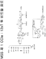
- G06F—ELECTRIC DIGITAL DATA PROCESSING
- G06F13/00—Interconnection of, or transfer of information or other signals between, memories, input/output devices or central processing units
- G06F13/38—Information transfer, e.g. on bus
- G06F13/42—Bus transfer protocol, e.g. handshake; Synchronisation
- G06F13/4282—Bus transfer protocol, e.g. handshake; Synchronisation on a serial bus, e.g. I2C bus, SPI bus
-
- H—ELECTRICITY
- H03—ELECTRONIC CIRCUITRY
- H03M—CODING; DECODING; CODE CONVERSION IN GENERAL
- H03M13/00—Coding, decoding or code conversion, for error detection or error correction; Coding theory basic assumptions; Coding bounds; Error probability evaluation methods; Channel models; Simulation or testing of codes
- H03M13/03—Error detection or forward error correction by redundancy in data representation, i.e. code words containing more digits than the source words
- H03M13/05—Error detection or forward error correction by redundancy in data representation, i.e. code words containing more digits than the source words using block codes, i.e. a predetermined number of check bits joined to a predetermined number of information bits
- H03M13/09—Error detection only, e.g. using cyclic redundancy check [CRC] codes or single parity bit
- H03M13/095—Error detection codes other than CRC and single parity bit codes
- H03M13/096—Checksums
-
- G—PHYSICS
- G06—COMPUTING; CALCULATING OR COUNTING
- G06F—ELECTRIC DIGITAL DATA PROCESSING
- G06F11/00—Error detection; Error correction; Monitoring
- G06F11/07—Responding to the occurrence of a fault, e.g. fault tolerance
- G06F11/16—Error detection or correction of the data by redundancy in hardware
- G06F11/1675—Temporal synchronisation or re-synchronisation of redundant processing components
- G06F11/1679—Temporal synchronisation or re-synchronisation of redundant processing components at clock signal level
-
- G—PHYSICS
- G06—COMPUTING; CALCULATING OR COUNTING
- G06F—ELECTRIC DIGITAL DATA PROCESSING
- G06F11/00—Error detection; Error correction; Monitoring
- G06F11/22—Detection or location of defective computer hardware by testing during standby operation or during idle time, e.g. start-up testing
- G06F11/2205—Detection or location of defective computer hardware by testing during standby operation or during idle time, e.g. start-up testing using arrangements specific to the hardware being tested
- G06F11/221—Detection or location of defective computer hardware by testing during standby operation or during idle time, e.g. start-up testing using arrangements specific to the hardware being tested to test buses, lines or interfaces, e.g. stuck-at or open line faults
-
- G—PHYSICS
- G06—COMPUTING; CALCULATING OR COUNTING
- G06F—ELECTRIC DIGITAL DATA PROCESSING
- G06F11/00—Error detection; Error correction; Monitoring
- G06F11/30—Monitoring
- G06F11/3003—Monitoring arrangements specially adapted to the computing system or computing system component being monitored
- G06F11/3027—Monitoring arrangements specially adapted to the computing system or computing system component being monitored where the computing system component is a bus
-
- G—PHYSICS
- G06—COMPUTING; CALCULATING OR COUNTING
- G06F—ELECTRIC DIGITAL DATA PROCESSING
- G06F13/00—Interconnection of, or transfer of information or other signals between, memories, input/output devices or central processing units
- G06F13/38—Information transfer, e.g. on bus
- G06F13/42—Bus transfer protocol, e.g. handshake; Synchronisation
- G06F13/4282—Bus transfer protocol, e.g. handshake; Synchronisation on a serial bus, e.g. I2C bus, SPI bus
- G06F13/4291—Bus transfer protocol, e.g. handshake; Synchronisation on a serial bus, e.g. I2C bus, SPI bus using a clocked protocol
-
- G—PHYSICS
- G06—COMPUTING; CALCULATING OR COUNTING
- G06F—ELECTRIC DIGITAL DATA PROCESSING
- G06F2213/00—Indexing scheme relating to interconnection of, or transfer of information or other signals between, memories, input/output devices or central processing units
- G06F2213/0016—Inter-integrated circuit (I2C)
Abstract
공유된 버스를 통하여 에러 검출 최적화를 용이하게 하는 것에 대하여 지시된 여러 양태들이 개시되어 있다. 마스터 디바이스는 슬레이브 디바이스에 커플링되고, 워드의 인코딩된 통신은 제어 데이터 버스를 통하여 마스터 디바이스와 슬레이브 디바이스 사이에서 용이하게 된다. 인코딩된 통신은 에러 검출 상수를 최대화하는 것을 용이하게 하기 위해 인코딩된 통신의 복수의 최하위 비트들을 할당하는 프로토콜에 따라 인코딩된다. 프로토콜은 워드의 데이터 부분의 적어도 제 1 최상위 비트 또는 적어도 하나의 추가적인 에러 검출 비트를 포함하기 위해 복수의 최하위 비트들을 할당한다.Various aspects are directed to facilitating error detection optimization via a shared bus. The master device is coupled to the slave device, and the encoded communication of the word is facilitated between the master device and the slave device via the control data bus. The encoded communication is encoded according to a protocol that allocates a plurality of least significant bits of the encoded communication to facilitate maximizing the error detection constant. The protocol allocates a plurality of least significant bits to include at least a first most significant bit of the data portion of the word or at least one additional error detection bit.

Description
관련 출원들의 상호 참조Cross reference of related applications
본 출원은 2014년 2월 28일 출원된 미국 특허 가출원 제 61/946,647 호 및 2015년 2월 27일 출원된 미국 특허 비-가출원 제 14/634,106 호를 우선권으로 주장하며, 여기서는 그 전체 내용을 참조로서 포함한다.This application claims priority from U.S. Provisional Patent Application Serial No. 61 / 946,647, filed February 28, 2014, and U.S. Patent Application No. 14 / 634,106, filed February 27, 2015, which is hereby incorporated by reference in its entirety .
기술분야Technical field
본 개시물은 공유된 버스를 통한 효율적인 동작들을 실시하는 것에 관한 것으로, 보다 구체적으로, 공유된 버스를 통한 에러 검출 최적화를 용이하게 하기 위해 원하는 워드 포맷에 따라 비트들을 할당하는 것에 관한 것이다.This disclosure relates to implementing efficient operations over a shared bus, and more particularly, to allocating bits according to a desired word format to facilitate error detection optimization over a shared bus.
일반적으로 공유된 버스는 다수의 디바이스들을 커플링할 때 이용될 수도 있다. 예를 들어, 인터-집적 회로 (I2C 그리고 또한 I2C 로서 지칭됨) 는 마더보드, 임베디드 시스템, 셀폰 또는 다른 전자 디바이스들에 저속 주변 기기들을 연결하는데 이용되는 멀티-마스터 시리얼 단일단 버스이다. I2C 버스는 7-비트 어드레싱을 갖는 시리얼 클록 라인 (SCL) 및 시리얼 데이터 라인 (SDA) 을 포함한다. I2C 버스는 노드들에 대하여 두개의 역할들: 마스터 및 슬레이브를 갖는다. 마스터 노드는 클록을 생성하고 슬레이브 노드들과의 통신을 개시하는 노드이다. 슬레이브 노드는 마스터에 의해 어드레싱될 때 클록을 수신하여 응답하는 노드이다. I2C 버스는 임의의 수의 마스터 노드들이 존재할 수 있음을 의미하는 멀티-마스터 버스이다. 추가적으로, 마스터 및 슬레이브 역할들은 메시지들 간에 (즉, "STOP" 이 전송된 후에) 변경될 수도 있다. I2C 는 메시지들의 기본 유형들을 정의하며, 이들 각각은 START 로 시작하여 STOP 으로 종료한다.In general, a shared bus may be used to couple multiple devices. For example, an inter-integrated circuit (I2C, and also referred to as I 2 C) is a motherboard, embedded systems, cell phones or multi used to connect the low-speed peripheral devices to the other electronic device, the master serial stage is one bus. The I2C bus includes a serial clock line (SCL) and a serial data line (SDA) with 7-bit addressing. The I2C bus has two roles: master and slave for the nodes. The master node is a node that generates the clock and initiates communication with the slave nodes. A slave node is a node that receives and responds to a clock when addressed by the master. The I2C bus is a multi-master bus, which means that any number of master nodes may be present. Additionally, the master and slave roles may change between messages (i.e., after "STOP" is sent). I2C defines the basic types of messages, each of which starts with START and ends with STOP.
카메라 구현의 문맥에서, 단방향 송신들은 이미지 센서로부터 이미지를 캡처하고, 대응하는 이미지 데이터를 기저대역 프로세서에서의 메모리에 송신하는데 이용될 수도 있는 한편, 제어 데이터는 기저대역 프로세서 및 이미지 센서 뿐만 아니라 다른 주변 디바이스들 사이에서 교환될 수도 있다. 일 예에서, 카메라 제어 인터페이스 (CCI) 프로토콜은 기저대역 프로세서와 이미지 센서 (및/또는 하나 이상의 슬레이브 노드들) 사이에서 이러한 제어 데이터에 이용될 수도 있다. 다른 예에서, CCI 프로토콜은 I2C 시리얼 버스를 통하여 이미지 센서와 기저대역 프로세서 사이에서 구현될 수도 있다.In the context of a camera implementation, unidirectional transmissions may be used to capture an image from an image sensor and transmit the corresponding image data to memory in the baseband processor, while the control data may be transmitted to the baseband processor and the image sensor, May be exchanged between the devices. In one example, a Camera Control Interface (CCI) protocol may be used for such control data between the baseband processor and the image sensor (and / or one or more slave nodes). In another example, the CCI protocol may be implemented between an image sensor and a baseband processor via an I2C serial bus.
에러 검출 알고리즘들은 종종 공유된 버스 통신들의 정확도를 개선하도록 구현된다. 이러한 에러들은 그러나 종종 통상의 에러 검출 알고리즘들에 의해 검출되지 않는다. 따라서, 공유된 버스 상에서 통신된 에러들이 보다 정확하게 검출되는 알고리즘을 구현하는 것이 바람직하다.Error detection algorithms are often implemented to improve the accuracy of shared bus communications. These errors, however, are often not detected by conventional error detection algorithms. It is therefore desirable to implement an algorithm in which errors communicated on a shared bus are detected more accurately.
다음은 이러한 양태들의 기본적인 이해를 제공하기 위해 본 개시물의 하나 이상의 양태들의 단순화된 개요를 제공한다. 본 개요는 본 개시물의 모든 예견되는 피처들의 확장적인 개요가 아니며, 본 개시물의 모든 양태들의 주요한 또는 중요한 엘리먼트들을 식별하도록 의도된 것도 아니고 본 개시물의 임의의 또는 모든 양태들의 범위를 기술하도록 의도된 것도 아니다. 유일한 목적은 하기에 제시되는 상세한 설명에 대한 전조로서 본 개시물의 하나 이상의 양태들의 몇몇 개념들을 단순화된 형태로 제공하는 것이다.The following provides a simplified overview of one or more aspects of the disclosure to provide a basic understanding of such aspects. This summary is not an extensive overview of all the contemplated features of the disclosure, nor is it intended to identify key or critical elements of all aspects of the disclosure, nor is it intended to describe the scope of any or all aspects of the disclosure no. Its sole purpose is to present some concepts of one or more aspects of the disclosure in a simplified form as a prelude to the more detailed description that is presented later.
본 개시물의 양태들은 공유된 버스를 통하여 에러 검출 최적화를 용이하게 하는 것을 향하여 지시되는 방법들, 장치들, 컴퓨터 프로그램 제품들, 및 프로세싱 시스템들을 제공한다. 일 양태에서, 본 개시물은 마스터 디바이스를 슬레이브 디바이스에 커플링하는 것, 및 제어 데이터 버스를 통한 마스터 디바이스와 슬레이브 디바이스 사이에서의 워드의 인코딩된 통신을 용이하게 하는 것을 포함하는 방법을 제공한다. 이 특정 구현을 위하여, 인코딩된 통신은 에러 검출 상수를 최대화하는 것을 용이하게 하기 위해 인코딩된 통신의 복수의 최하위 비트들을 할당하는 프로토콜에 따라 인코딩된다. 여기에서, 이러한 최대화는 워드의 데이터 부분의 적어도 제 1 최상위 비트 또는 적어도 하나의 추가적인 에러 검출 비트를 포함하기 위해 복수의 최하위 비트들을 할당하는 프로토콜을 통하여 실현된다.Aspects of the present disclosure provide methods, apparatus, computer program products, and processing systems directed towards facilitating error detection optimization via a shared bus. In one aspect, the disclosure provides a method comprising coupling a master device to a slave device, and facilitating encoded communication of the word between the master device and the slave device via the control data bus. For this particular implementation, the encoded communication is encoded according to a protocol that allocates a plurality of least significant bits of the encoded communication to facilitate maximizing the error detection constant. Here, this maximization is realized through a protocol that allocates a plurality of least significant bits to include at least a first most significant bit of the data portion of the word or at least one additional error detection bit.
다른 양태에서, 공유된 버스를 통하여 에러 검출 최적화를 용이하게 하도록 구성되는 디바이스가 개시된다. 디바이스는 제어 데이터 버스에 커플링된 프로세서를 포함한다. 여기에서, 프로세서는 제어 데이터 버스를 통하여 마스터 디바이스와 슬레이브 디바이스 사이의 워드의 인코딩된 통신을 용이하게 하도록 구성된다. 이 구현에서의 인코딩된 통신은 에러 검출 상수를 최대화하는 것을 용이하게 하기 위해 인코딩된 통신의 복수의 최하위 비트들을 할당하는 프로토콜에 따라 인코딩된다. 특히, 프로토콜은 워드의 데이터 부분의 적어도 제 1 최상위 비트 또는 적어도 하나의 추가적인 에러 검출 비트를 포함하기 위해 복수의 최하위 비트들을 할당한다.In another aspect, a device is disclosed that is configured to facilitate error detection optimization via a shared bus. The device includes a processor coupled to the control data bus. Wherein the processor is configured to facilitate encoded communication of the word between the master device and the slave device via the control data bus. The encoded communication in this implementation is encoded according to a protocol that allocates a plurality of least significant bits of the encoded communication to facilitate maximizing the error detection constant. In particular, the protocol allocates a plurality of least significant bits to include at least a first most significant bit of the data portion of the word or at least one additional error detection bit.
추가의 양태에서, 공유된 버스를 통하여 에러 검출 최적화를 용이하게 하도록 구성되는 다른 디바이스가 개시된다. 이 구현에서, 디바이스는 마스터 디바이스를 슬레이브 디바이스에 커플링하는 수단, 및 제어 데이터 버스를 통한 마스터 디바이스와 슬레이브 디바이스 사이에서의 워드의 인코딩된 통신을 용이하게 하는 수단을 포함한다. 여기에서, 인코딩된 통신은 에러 검출 상수를 최대화하는 것을 용이하게 하기 위해 인코딩된 통신의 복수의 최하위 비트들을 할당하는 프로토콜에 따라 인코딩된다. 즉, 프로토콜은 워드의 데이터 부분의 적어도 제 1 최상위 비트 또는 적어도 하나의 추가적인 에러 검출 비트를 포함하기 위해 복수의 최하위 비트들을 할당한다.In a further aspect, another device is disclosed that is configured to facilitate error detection optimization over a shared bus. In this implementation, the device includes means for coupling the master device to the slave device, and means for facilitating encoded communication of the word between the master device and the slave device over the control data bus. Here, the encoded communication is encoded according to a protocol that allocates a plurality of least significant bits of the encoded communication to facilitate maximizing the error detection constant. That is, the protocol allocates a plurality of least significant bits to include at least the first most significant bit or at least one additional error detection bit of the data portion of the word.
또 다른 양태에서, 상부에 저장된 하나 이상의 명령들을 통하여 공유된 버스 상에서 에러 검출 최적화를 용이하게 하도록 구성되는 비일시적 머신 판독가능 저장 매체가 개시되어 있다. 여기에서, 적어도 하나의 프로세서에 의해 실행될 때, 하나 이상의 명령들은 적어도 하나의 프로세서로 하여금, 마스터 디바이스를 슬레이브 디바이스에 커플링하게 하고, 그리고 제어 데이터 버스를 통한 마스터 디바이스와 슬레이브 디바이스 사이에서의 워드의 인코딩된 통신을 용이하게 한다. 이 구현에서, 인코딩된 통신은 에러 검출 상수를 최대화하는 것을 용이하게 하기 위해 인코딩된 통신의 복수의 최하위 비트들을 할당하는 프로토콜에 따라 인코딩된다. 특히, 프로토콜은 워드의 데이터 부분의 적어도 제 1 최상위 비트 또는 적어도 하나의 추가적인 에러 검출 비트를 포함하기 위해 복수의 최하위 비트들을 할당한다.In another aspect, a non-transitory machine-readable storage medium is disclosed that is configured to facilitate error detection optimization on a shared bus via one or more instructions stored thereon. Wherein when executed by the at least one processor, the one or more instructions cause at least one processor to cause the master device to couple to the slave device and to cause the at least one processor to < RTI ID = Facilitates encoded communication. In this implementation, the encoded communication is encoded according to a protocol that allocates a plurality of least significant bits of the encoded communication to facilitate maximizing the error detection constant. In particular, the protocol allocates a plurality of least significant bits to include at least a first most significant bit of the data portion of the word or at least one additional error detection bit.
이들 및 다른 개시된 양태들은 다음에 오는 상세한 설명의 검토시 보다 완전하게 이해될 것이다. 본 발명의 다른 양태들, 특징들, 및 실시형태들은, 다음의 상세한 설명, 첨부 도면들과 연계한 본 발명의 예시적인 양태들을 검토할 시에, 당업자들에게 자명해질 것이다. 본 발명의 피처들이 하기에서 소정의 양태들 및 도면들에 대해 논의될 수도 있지만, 본 발명의 모든 양태들은 본원에서 논의된 유리한 피처들 중 하나 이상의 유리한 피처들을 포함할 수 있다. 다시 말해, 하나 이상의 양태들이 소정의 유리한 피처들을 갖는 것으로 논의될 수도 있으나, 이러한 피처들 중 하나 이상의 피처들은 또한 본원에서 논의된 발명의 다양한 양태들에 따라 이용될 수도 있다. 유사한 방식으로, 예시적인 양태들이 디바이스, 시스템, 또는 방법 양태들로 하기에서 논의될 수도 있으나, 이러한 예시적인 양태들은 다양한 디바이스들, 시스템들, 및 방법들로 구현될 수도 있음이 이해되어야 한다.These and other disclosed aspects will be more fully understood upon review of the following detailed description. Other aspects, features, and embodiments of the present invention will become apparent to those skilled in the art upon review of the following detailed description, upon exemplary aspects of the invention in connection with the accompanying drawings. Although the features of the present invention may be discussed below with respect to certain aspects and drawings, all aspects of the present invention may include advantageous features of one or more of the advantageous features discussed herein. In other words, one or more aspects may be discussed as having certain advantageous features, but one or more of these features may also be utilized in accordance with various aspects of the invention discussed herein. In a similar manner, it is to be understood that the exemplary aspects may be discussed below in terms of devices, systems, or method aspects, but it should be understood that these exemplary aspects may be implemented in various devices, systems, and methods.
여러 피처들, 속성, 및 이점들은 유사한 도면 부호들이 전체에 걸쳐 대응하게 식별하는 도면들과 함께 취해진 경우 하기에 제시된 상세한 설명으로부터 보다 명백해질 것이다.
도 1 은 본 개시물의 양태에 따른 예시적인 멀티-마스터 버스를 예시한다.
도 2 는 본 개시물의 양태에 따른 예시적인 마스터/슬레이브 디바이스의 블록도이다.
도 3 은 기저대역 프로세서 및 이미지 센서를 갖고 이미지 데이터 버스 및 멀티-모드 제어 데이터 버스를 구현하는 디바이스를 예시하는 블록도이다.
도 4 는 CCIe 모드에서의 심볼 투 심볼 트랜지션들 내에 어떻게 임베딩되어, 데이터 송신들에 대해 I2C 버스에서의 2 개의 라인들 (즉, SDA 라인 및 SCL 라인) 의 이용을 허용할 수 있는지의 방법을 예시한다.
도 5 는 트랜스코딩된 심볼들 내에 클록 신호를 임베딩하기 위해 송신기에서 데이터 비트들의 트랜스코딩된 심볼들로의 트랜스코딩을 위한 예시적인 방법을 예시하는 블록도이다.
도 6 은 트랜지션 넘버들과 순차적 심볼들 사이의 예시적인 변환을 예시한다.
도 7 은 트랜지션 넘버들과 순차적 심볼들 사이의 변환을 예시한다.
도 8 은 최상위 비트로부터 최하위 비트로 2진 비트들을 3진수들로 변환하는 방법을 예시한다.
도 9 는 최상위 비트로부터 최하위 비트로 2진 비트들을 3진수들로 변환하기 위한 송신기측 로직 회로를 예시한다.
도 10 은 최상위 비트로부터 최하위 비트로 3진수들을 2진 비트들로 변환하기 위한 방법을 예시한다.
도 11 은 12 디지트 3진수를 20 비트들로 변환하는 수신기측 로직 회로를 예시한다.
도 12 는 비트 19 (즉, 비트 카운트가 비트 0 인 제 1 비트에서 시작할 때 제 20 비트) 가 CCIe 프로토콜에는 주로 미사용되고 공유 버스 상에서 디바이스들 사이의 커맨드들에 이용될 수도 있는 것을 개념적으로 예시한다.
도 13 은 공유 버스가 I2C 모드로부터 CCIe 모드로 동작하도록 스위칭됨을 슬레이브 디바이스들에 표시하기 위해 공유 버스를 통하여 마스터 디바이스에 의해 전송될 수도 있는 CCIe 모드 엔트리 표시자에 대한 예시적인 일반 호출을 예시한다.
도 14 는 CCIe 모드로부터 I2C 모드로의 트랜지션을 모든 CCIe 에이블 디바이스들에 표시하기 위해 CCIe 마스터 디바이스 (예를 들어, I2C 모드에 있기는 하지만 도 1 에서의 마스터 디바이스) 에 의해 발행될 수도 있는 예시적인 CCIe 호출을 예시한다.
도 15 는 예시적인 CCIe 슬레이브 식별자 (SID) 워드 포맷을 예시한다.
도 16 은 예시적인 CCIe 어드레스 워드 포맷을 예시한다.
도 17 은 예시적인 기록 데이터 워드 포맷을 예시한다.
도 18 은 예시적인 판독 사양 워드 포맷을 예시한다.
도 19 는 예시적인 판독 데이터 워드 포맷을 예시한다.
도 20 은 I2C 1 바이트 기록 데이터 동작의 예시적인 타이밍도를 예시한다.
도 20 은 데이터 비트들이 SDA 라인 및 SCL 라인을 통한 송신에 대하여 12 개의 심볼들로 트랜스코딩된 예시적인 CCIe 송신을 예시한다.
도 22 는 본원에 예시된 인코딩 방식으로부터 야기되는 제 20 비트 (비트 19) 의 예시적인 맵핑을 예시한다.
도 23 은 도 22 의 제 20 비트 (비트 19) 의 예시적인 맵핑 내에서의 서브영역의 세부사항들을 예시한다.
도 24 는 발생할 수도 있는 여러 심볼 에러 조건들을 예시한다.
도 25 는 송신된 심볼 시퀀스 (0321_0321_0321)(이는 2진 시퀀스 (0000_0000_0000_0000_0000) 및 3진수 (0000_0000_00003) 로 트랜슬레이션함) 에서 가능한 에러들, 및 이러한 에러들이 3 개의 최하위 비트들 내에서 어떻게 검출가능한지의 방법을 나타내는 테이블을 예시한다.
도 26 은 송신된 심볼 시퀀스 (2301_2301_2301)(이는 2진 시퀀스 (0100_0000_1101_1111_1000) 및 3진수 (1111_1111_11113) 로 트랜슬레이션함) 에서 가능한 에러들, 및 이러한 에러들이 3 개의 최하위 비트들 내에서 어떻게 검출가능한지의 방법을 나타내는 테이블을 예시한다.
도 27 은 송신된 심볼 시퀀스 (3131_3131_3131)(이는 2진 시퀀스 (1000_0001_1011_1111_0000) 및 3진수 (2222_2222_22223) 로 트랜슬레이션함) 에서 가능한 에러들, 및 이러한 에러들이 3 개의 최하위 비트들 내에서 어떻게 검출가능한지의 방법을 나타내는 테이블을 예시한다.
도 28 은 송신된 심볼 시퀀스 (0132_3101_3231) 에서 가능한 에러들, 및 이러한 에러들이 3 개의 최하위 비트들 내에서 어떻게 검출가능한지의 방법을 나타내는 테이블을 예시한다.
도 29 는 송신된 심볼 시퀀스 (2030_2120_3021) 에서 가능한 에러들, 및 이러한 에러들이 3 개의 최하위 비트들 내에서 어떻게 검출가능한지의 방법을 나타내는 테이블을 예시한다.
도 30 은 송신된 심볼 시퀀스 (3231_0132_3101) 에서 가능한 에러들, 및 이러한 에러들이 3 개의 최하위 비트들 내에서 어떻게 검출가능한지의 방법을 나타내는 테이블을 예시한다.
도 31 은 본 개시물에 따라 제공되는 마스터/슬레이브 디바이스의 예시적인 컴포넌트들을 예시하는 블록도이다.
도 32 는 본 개시물의 일 양태에 따른 예시적인 인코딩/디코딩 방법론을 예시하는 흐름도이다.
도 33 은 본 개시물의 일 양태에 따른 예시적인 인코더 컴포넌트들을 예시하는 블록도이다.
도 34 는 본 개시물의 일 양태에 따른 예시적인 인코딩 방법론을 예시하는 흐름도이다.
도 35 는 본 개시물의 일 양태에 따른 예시적인 디코더 컴포넌트들을 예시하는 블록도이다.
도 36 은 본 개시물의 일 양태에 따른 예시적인 디코딩 방법론을 예시하는 흐름도이다.The various features, attributes, and advantages will become more apparent from the detailed description set forth below when taken in conjunction with the drawings that identify like reference numerals throughout.
1 illustrates an exemplary multi-master bus in accordance with aspects of the present disclosure.
2 is a block diagram of an exemplary master / slave device in accordance with aspects of the present disclosure.
3 is a block diagram illustrating a device having a baseband processor and an image sensor and implementing an image data bus and a multi-mode control data bus.
Figure 4 illustrates by way of example how it can be embedded within symbol-to-symbol transitions in CCIe mode to allow the use of two lines (i.e., SDA line and SCL line) on the I2C bus for data transmissions do.
5 is a block diagram illustrating an exemplary method for transcoding data bits from a transmitter to transcoded symbols for embedding a clock signal within transcoded symbols.
Figure 6 illustrates an exemplary transformation between transition numbers and sequential symbols.
Figure 7 illustrates the transition between transition numbers and sequential symbols.
8 illustrates a method of converting binary bits to trinary numbers from the most significant bit to the least significant bit.
Figure 9 illustrates a transmitter side logic circuit for converting binary bits to most significant bits from the most significant bit to the least significant bit.
10 illustrates a method for transforming trinary numbers from the most significant bit to the least significant bit into binary bits.
Figure 11 illustrates a receiver side logic circuit that converts a 12 digit triplet to 20 bits.
Figure 12 conceptually illustrates that bit 19 (i.e., the twentieth bit when the bit count starts at bit one) is largely unused in the CCIe protocol and may be used for commands between devices on a shared bus .
Figure 13 illustrates an exemplary general call to a CCIe mode entry indicator that may be sent by the master device over the shared bus to indicate to the slave devices that the shared bus is switched to operate in the I2C mode to the CCIe mode.
FIG. 14 shows an example (not shown) that may be issued by a CCIe master device (e.g., in the I2C mode but the master device in FIG. 1) to display a transition from the CCIe mode to the I2C mode on all CCIe enabled devices It illustrates the CCIe call.
15 illustrates an exemplary CCIe slave identifier (SID) word format.
Figure 16 illustrates an exemplary CCIe address word format.
17 illustrates an exemplary write data word format.
Figure 18 illustrates an exemplary read specification word format.
19 illustrates an exemplary read data word format.
Figure 20 illustrates an exemplary timing diagram of I2C 1-byte write data operation.
20 illustrates an exemplary CCIe transmission in which the data bits are transcoded into 12 symbols for transmission over the SDA and SCL lines.
22 illustrates an exemplary mapping of the twentieth bit (bit 19) resulting from the encoding scheme illustrated herein.
FIG. 23 illustrates the details of the sub-region within the exemplary mapping of the twentieth bit (bit 19) of FIG.
Figure 24 illustrates several symbol error conditions that may occur.
Figure 25 shows the possible errors in the transmitted symbol sequence (0321_0321_0321) (which translates to binary sequence (0000_0000_0000_0000_0000) and trinary number (0000_0000_0000 3 )) and how these errors are detectable in the three least significant bits A table showing the method of FIG.
Figure 26 shows the possible errors in the transmitted symbol sequence 2301_2301_2301 (which translates to binary sequence (0100_0000_1101_1111_1000) and ternary (1111_1111_1111 3 )) and how these errors are detectable in the three least significant bits A table showing the method of FIG.
Figure 27 shows possible errors in the transmitted symbol sequence 3131_3131_3131 (which translates to binary sequence 1000_0001_1011_1111_0000 and ternary 2222_2222_2222 3 ), and how these errors are detectable in the three least significant bits A table showing the method of FIG.
Fig. 28 illustrates possible errors in the transmitted symbol sequence (0132_3101_3231), and a table showing how these errors can be detected within the three least significant bits.
FIG. 29 illustrates possible errors in the transmitted symbol sequence 2030_2120_3021, and a table showing how these errors can be detected within the three least significant bits.
Figure 30 illustrates possible errors in the transmitted symbol sequence 3231_0132_3101, and a table showing how these errors can be detected within the three least significant bits.
31 is a block diagram illustrating exemplary components of a master / slave device provided in accordance with the present disclosure.
32 is a flow chart illustrating an exemplary encoding / decoding methodology in accordance with an aspect of the present disclosure.
33 is a block diagram illustrating exemplary encoder components in accordance with an aspect of the disclosure.
34 is a flow chart illustrating an exemplary encoding methodology in accordance with an aspect of the present disclosure.
35 is a block diagram illustrating exemplary decoder components in accordance with an aspect of the present disclosure.
Figure 36 is a flow chart illustrating an exemplary decoding methodology in accordance with an aspect of the present disclosure.
다음의 설명에서, 실시형태들의 완전한 이해를 제공하기 위해 특정 세부사항들이 주어진다. 그러나, 실시형태들은 이러한 특정 세부사항들이 없이 실시될 수도 있음이 당업자에 의해 이해될 것이다. 예를 들어, 실시형태들을 불필요한 상세로 불명확하게 하지 않기 위해 회로들을 블록도들로 도시할 수도 있다. 다른 경우들에서, 실시형태들을 불명확하게 하지 않기 위해 공지의 회로들, 구조들 및 기술들이 상세히 도시될 수도 있다.
In the following description, specific details are given to provide a thorough understanding of the embodiments. However, it will be understood by those skilled in the art that embodiments may be practiced without these specific details. For example, circuits may be shown in block diagrams in order not to obscure the embodiments with unnecessary detail. In other instances, well-known circuits, structures and techniques may be shown in detail in order not to obscure the embodiments.
개관survey
배경기술에서 논의된 바와 같이, 종래의 에러 검출 알고리즘들의 제약들로 인하여, 공유된 버스를 통한 에러들을 종종 놓칠 수 있다. 본원에 개시된 양태들은 에러 검출 최적화를 용이하게 하기 위해 원하는 워드 포맷에 따라 비트들을 할당하는 것에 의해 이러한 제약들을 극복하는 것에 대하여 개시된다. 즉, 공유된 버스 통신들에 대한 유연성있는 워드 포맷을 이용하는 것에 대하여 지시되는 양태들이 개시되며, 여기에서, 추가적인 에러 검출 비트들이 에러 검출 최적화를 용이하게 하기 위해 전략적으로 할당될 수도 있다.As discussed in the background, due to the limitations of conventional error detection algorithms, errors over shared buses can often be missed. The aspects disclosed herein are disclosed for overcoming these limitations by allocating bits according to the desired word format to facilitate error detection optimization. That is, aspects directed to utilizing a flexible word format for shared bus communications are disclosed, wherein additional error detection bits may be strategically assigned to facilitate error detection optimization.
다음 도 1 을 참조하여 보면, 본원에 개시된 에러 검출 최적화 양태를 용이하게 하는 예시적인 멀티-마스터 버스 아키텍처가 제공된다. 예시된 바와 같이, 복수의 마스터/슬레이브 디바이스들 (110, 120, 130, 및 140) 이 공유된 버스 (100) 를 통하여 서로 커플링된다. 여기에서, 공유된 버스 (100) 는 멀티-마스터 버스이며, 마스터/슬레이브 디바이스들 (110, 120, 130, 및 140) 중 어느 것이 마스터 디바이스 또는 슬레이브 디바이스로서 동작할 수도 있다. 이 특정 예에서, 마스터/슬레이브 디바이스 (120) 는 공유된 버스 (100) 를 통하여 다른 마스터/슬레이브 디바이스들 (110, 130, 및 140) 에 워드 (122) 를 송신하고, 여기에서, 워드 (122) 는 에러 검출을 최적화하는 비트 할당 방식에 따라 마스터/슬레이브 디바이스 (120) 에 의해 인코딩된다. 예를 들어, 이러한 방식은 비최적화된 방식으로 할당된 에러 검출 비트들의 수에 대하여 가장 큰 수의 에러 검출 비트들을 할당하는 것에 의해 에러 검출을 최적화할 수도 있다. 워드 (122) 를 적절하게 디코딩하기 위하여, 이에 따라, 워드 (122) 가 에러 검출 최적화로 인코딩되었는지의 여부를 마스터/슬레이브 디바이스들 (110, 130, 및 140) 이 검출하고, 그 후 워드 (122) 는 대응하는 비트 할당 방식에 기초하여 디코딩되는 것으로 고려된다.Referring now to FIG. 1, an exemplary multi-master bus architecture is provided that facilitates the error detection optimization aspects disclosed herein. As illustrated, a plurality of master /
도 2 에는, 본 개시물의 양태에 따른 예시적인 마스터/슬레이브 디바이스의 블록도가 제공된다. 예시된 바와 같이, 마스터/슬레이브 디바이스 (200) 는 인코더 컴포넌트 (210), 디코더 컴포넌트 (220) 및 통신 컴포넌트 (230) 를 포함한, 본원에 개시된 에러 검출 최적화들을 수행하는 것을 용이하게 하는 여러 컴포넌트들을 포함한다. 마스터/슬레이브 디바이스 (200) 는 예를 들어, 도 1 에 예시된 마스터/슬레이브 디바이스들 (110, 120, 130, 및 140) 의 어느 것을 포함하는 본원에 포함된 임의의 마스터/슬레이브 디바이스로서 구성될 수도 있는 것으로 고려된다. 예를 들어, 통신 컴포넌트 (230) 는 공유된 버스를 통하여 통신되는 워드들을 송신 및 수신하도록 구성될 수도 있고, 인코더 컴포넌트 (210) 는 추가적인 에러 검출 비트들을 포함하도록 워드들을 인코딩하는 것에 의해 에러 검출을 최적화하도록 구성되고, 디코더 컴포넌트 (220) 는 이들 추가적인 에러 검출 비트들을 포함하는 워드들을 디코딩하도록 구성되는 것으로 고려된다.In Figure 2, a block diagram of an exemplary master / slave device in accordance with aspects of the present disclosure is provided. Master /
본 개시물의 특정 양태에서, 마스터/슬레이브 디바이스 (200) 는 CCI 프로토콜에 따라 워드들을 인코딩/디코딩하도록 구성된다. 이를 위하여, 2진수를 3진수로 변환하고 그 후 3진수가 I2C 버스를 통한 송신을 위해 클록과 함께 임베딩되는 심볼들로 트랜스코딩되어, 이전의 것보다 더 높은 속도를 가능하게 하는 CCIe (Camera Control Interface extended) 라 지칭되는 CCI 에 대한 확장안이 개발되고 있음을 주지한다. 에시적인 구현에서, 20-비트 2진수들은 3진수 컨버터 (즉, 비트들-투-12xT 컨버터) 에 병렬하는 입력이다. 모든 바이너리 비트들을 수신한 후, 3진수 컨버터는 대응하는 3 진수를 출력한다. 그 후, 출력 넘버가 동일한 방식을 트랜스코더에 전송된다. 본원에 개시된 CCIe 의 양태에서, 3진 트랜지션 넘버의 순차적 심볼로의 변환은 심볼 바이 심볼 기반으로 수행되고, 이는 바람직하게 다수의 심볼들을 동시에 프로세싱하는 것보다 덜 하드웨어 리소스들을 요구한다. 그 후, 심볼들은 버스를 통하여 송신된다.In certain aspects of the disclosure, the master /
3진수 공간의 이용 및 심볼들로의 변환은 엑스트라 비트가 이용가능하도록 한다. 일 예에서, 이 엑스트라 비트는 3 진수들의 영역이 달리 이용가능하지 않은 다른 기능성을 지원하기 위해 이용가능하게 되도록 하는 최상위 비트일 수도 있다. 예를 들어, 에러 검출, 핫-플러그 기능 및/또는 SID 스캐닝은 이 엑스트라 비트에 포함될 수도 있는 엑스트라 정보로 인하여 모두 용이하게 될 수도 있다.Use of the ternary space and conversion to symbols makes the extra bits available. In one example, this extra bit may be the most significant bit such that the area of the triples is made available to support other functionality not otherwise available. For example, error detection, hot-plug functionality, and / or SID scanning may all be facilitated due to extra information that may be included in this extra bit.
예시적인 동작 환경Exemplary operating environment
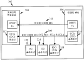
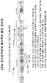
도 3 은 기저대역 프로세서 (304) 및 이미지 센서 (306) 를 갖고 이미지 데이터 버스 (316) 및 멀티-모드 제어 데이터 버스 (308) 를 구현하는 디바이스 (302) 를 예시하는 블록도이다. 도 3 은 카메라 디바이스 내에서의 멀티-모드 제어 데이터 버스 (308) 를 예시하고 있지만, 이 제어 데이터 버스 (308) 는 여러 상이한 디바이스들 및/또는 시스템들에서 구현될 수도 있음을 명확히 해야 한다. 이미지 데이터는 이미지 센서 (306) 로부터 기저대역 프로세서 (304) 로 이미지 데이터 버스 (316)(예를 들어, 고속 차동 DPHY 링크) 를 통하여 송신될 수도 있다.3 is a block diagram illustrating a
일 예에서, 제어 데이터 버스 (308) 는 2 개의 와이어들, 클록 라인 (SCL) 및 시리얼 데이터 라인 (SDA) 을 포함하는 I2C 버스일 수도 있다. 클록 라인 (SCL) 은 I2C 버스 (제어 데이터 버스 (308)) 를 통하여 모든 데이터 트랜스퍼들을 동기시키는데 이용되는 클록을 전송하는데 이용될 수도 있다. 데이터 라인 (SDA) 및 클록 라인 (SCL) 은 I2C 버스 (제어 데이터 버스 (308)) 상에서 모든 디바이스들 (312, 314, 및 318) 에 커플링된다. 이 예에서, 제어 데이터는 제어 데이터 버스 (308) 을 통하여 기저대역 프로세서 (304) 및 이미지 센서 (306) 뿐만 아니라 다른 주변 디바이스들 (318, 322, 및/또는 324) 사이에서 교환될 수도 있다. I2C 에 대한 표준 클록 (SCL) 속도는 최대 100 KHz 이다. I2C 고속 모드에서의 표준 클록 (SCL) 속도는 최대 400 KHz 이고 I2C 고속 모드 플러스 (Fm+) 에서는 그 속도가 최대 1 MHz 이다. I2C 버스를 통한 이들 동작 모드들은 카메라 애플리케이션들에 대하여 이용될 때 카메라 제어 인터페이스 (CCI) 모드로 지칭될 수도 있다.In one example, the
일 양태에 따르면, (즉, 1 MHz 보다 더 큰 제어 데이터 버스 송신 주파수들을 갖는) 개선된 동작 모드가 멀티모드 제어 데이터 버스 (308) 를 통하여 카메라 동작을 지원하도록 구현될 수도 있다. I2C 버스를 통한 이 개선된 동작 모드는 카메라 애플리케이션들에 이용될 때, 카메라 제어 인터페이스 확장 (camera control interface extension; CCIe) 모드로서 지칭될 수도 있다. CCIe 모드에서, 클록이 2 개의 라인들을 통하여 심볼 투 심볼 트랜지션들에 임베딩되는 동안 SCL 라인 및 SDA 라인은 양쪽 모두 데이터를 송신하는데 이용될 수도 있다. 이 예에서, 기저대역 프로세서 (304) 는 마스터 디바이스 (312) 를 포함하고, 이미지 센서 (306) 는 슬레이브 노드 (314) 를 포함하며, 마스터 노드 (312) 와 슬레이브 노드 (314) 양쪽 모두는 제어 데이터 버스 (308) 에 커플링되는 다른 레거시 I2C 디바이스들의 적절한 동작에 영향을 주지 않고 카메라 제어 인터페이스 확장 (CCIe) 모드에 따라 제어 데이터 버스 (308) 를 통하여 동작할 수도 있다. 일 양태에 따르면, 제어 데이터 버스 (308) 를 통한 이 개선된 모드는 CCIe 디바이스들과 레거시 I2C 슬레이브 디바이스들 사이의 어떠한 브리지 디바이스 없이도 구현될 수도 있다.According to an aspect, an improved mode of operation may be implemented to support camera operation over the multimode control data bus 308 (i. E., With control data bus transmit frequencies greater than 1 MHz). This improved mode of operation over the I2C bus may be referred to as a camera control interface extension (CCIe) mode when used in camera applications. In CCIe mode, both the SCL line and the SDA line may be used to transmit data while the clock is embedded in the symbol-to-symbol transitions through the two lines. In this example, the
I2C-호환가능 디바이스들과 CCIe-호환가능 디바이스들이 공유 제어 데이터 버스 (308) 에 동시에 커플링되도록 허용하는 프로토콜이 제공된다. 제어 데이터 버스 (308) 는 별개의 통신 프로토콜들 (예를 들어, I2C 모드와 CCIe 모드) 에 따른 동작들 사이를 동적으로 스위칭할 수도 있다. 이전에 주지된 바와 같이, 공유 제어 데이터 버스 (308) 에 대한 통신들 및/또는 액세스는 멀티-모드 마스터 디바이스 (312) 에 의해 관리된다. 마스터 디바이스는 제어 데이터 버스 (308) 가 자신의 통신 프로토콜을 제 1 프로토콜 모드 (예를 들어, I2C 모드) 에서부터 제 2 프로토콜 모드 (예를 들어, CCIe 모드) 로 스위칭할 것임을 표시하기 위하여 진입 호출을 송신한다. 이와 유사하게, 마스터 디바이스는 제어 데이터 버스 (308) 가 자신의 통신 프로토콜을 제 2 프로토콜 모드 (예를 들어, CCIe 모드) 에서부터 제 2 프로토콜 모드 (예를 들어, I2C 모드) 로 스위칭할 것임을 표시하기 위하여 종료 호출을 송신한다. 공유된 버스 (308) 에 커플링된 슬레이브 디바이스들은 이들 진입 및 종료 호출들에 대하여 모니터링하여 이들이 공유된 버스 (308) 상에서 동작할 수도 있을 때를 확인한다.
A protocol is provided that allows I2C-compatible devices and CCIe-compatible devices to be coupled to the shared
예시적인 CCIe 인코딩 기술Exemplary CCIe encoding techniques
도 4 는 CCIe 모드에서의 심볼 투 심볼 트랜지션들 내에 어떻게 임베딩되어, 데이터 송신들에 대해 I2C 버스에서의 2 개의 라인들 (즉, SDA 라인 및 SCL 라인) 의 이용을 허용할 수 있는지의 방법을 예시한다. 일 예에서, 이 클록의 임베딩은 트랜지션 클록 트랜스코딩에 의해 실현될 수도 있다. 예를 들어, 물리적 링크 (와이어들) 를 통하여 송신될 데이터 (404) 가 트랜스코딩되어, 송신된 심볼들이 송신된 심볼들 (406) 의 트랜지션시 또는 매 심볼 사이클시에 상태를 변경하도록 보장된다. 일 예에서, 비트들의 시퀀스들이 3진수로 변환되고 3진수의 각각의 디지트는 송신을 위하여 심볼로 변환된다. 순차적 심볼들은 3진수의 2 개의 순차적 디지트들이 동일할 때에도 상이하게 되는 것이 보장된다. 그 결과, 오리지널 클록 (402) 은 매 심볼 사이클에서 심볼들의 상태들의 변경에 임베딩될 수도 있다. 수신기는 (송신된 심볼들 (406) 에서의) 각각의 심볼에서의 상태 트랜지션으로부터 클록 정보 (408) 를 복구한 다음, 송신된 심볼들 (406) 의 트랜스코딩을 반대로 하여 오리지널 데이터 (410) 를 획득한다. 일 예에서, 각각의 심볼은 디지트로 변환되고, 복수의 디지트들은 3진수를 구성하며, 여기에서 그 후, 3진수는 복수의 비트들로 변환된다. 그 결과, 오리지널 클록 (402) 은 매 심볼 사이클에서 심볼들의 상태들의 변경에 임베딩될 수도 있다. 이는 I2C 버스 (도 3 에서의 제어 데이터 버스 (SDA 라인 및 SCL 라인)) 의 양쪽 와이어들이 데이터 정보를 전송하는데 이용되도록 허용한다. 추가로, 심볼 레이트는 클록 및 데이터 신호들 사이의 세트업 및 홀드 시간을 더 이상 가질 필요가 없기 때문에 더블링될 수 있다.Figure 4 illustrates by way of example how it can be embedded within symbol-to-symbol transitions in CCIe mode to allow the use of two lines (i.e., SDA line and SCL line) on the I2C bus for data transmissions do. In one example, the embedding of this clock may be realized by transition clock transcoding. For example,
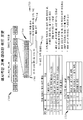
도 5 는 트랜스코딩된 심볼들 내에 클록 신호를 임베딩하기 위해 송신기에서 데이터 비트들의 트랜스코딩된 심볼들로의 트랜스코딩을 위한 예시적인 방법을 예시하는 블록도이다. 송신기 (502) 에서, 데이터 비트들 (504) 의 시퀀스는 3진수 (베이스 3) (즉, "트랜지션 넘버") 로 변환되고 그 후 3진수들은 클록 라인 (SCL)(512) 과 데이터 라인 (SDA)(514) 을 통하여 송신되는 (순차적) 심볼들로 변환된다.5 is a block diagram illustrating an exemplary method for transcoding data bits from a transmitter to transcoded symbols for embedding a clock signal within transcoded symbols. At the
일 예에서, 오리지널 20 비트들의 2진 데이터는 비트-투-트랜지션 넘버 컨버터 블록 (508) 에 입력되어, 12 디지트 3진수로 변환된다. 12 디지트 3진수의 각각의 디지트는 "트랜지션 넘버" 를 표현한다. 2 개의 연속하는 트랜지션 넘버들은 동일한 넘버들을 가질 수도 있다 (즉, 3진수의 연속하는 디지트들이 동일할 수도 있다). 각각의 트랜지션 넘버는 트랜지션 투 심볼 블록 (510) 에서 순차적 심볼로 변환되어, 2 개의 연속하는 순차적 심볼들이 동일한 값을 갖지 않게 된다. 트랜지션이 매 순차적 심볼에서 보장되기 때문에, 이러한 순차적 심볼 트랜지션은 클록 신호를 인베딩하도록 서브할 수도 있다. 그 후, 각각의 순차적 심볼 (516) 은 2 개의 와이어 물리적 링크 (예를 들어, SCL 라인 (512) 및 SDA 라인 (514) 을 포함하는 I2C 버스) 를 통하여 전송된다.In one example, the binary data of the original 20 bits is input to the bit-to-transition
도 6 은 트랜지션 넘버들 (602) 과 순차적 심볼들 (604) 사이의 예시적인 변환을 예시한다. 트랜지션 넘버로서 또한 지칭되는 3진수, 베이스-3 넘버의 개별적인 디지트는 세 (3) 개의 가능한 디지트들 또는 상태들, 0, 1, 또는 2 중 하나를 가질 수 있다. 동일한 디지트가 3진수의 2 개의 연속하는 디지트들에 나타날 수도 있는 한편, 2 개의 연속하는 순차적 심볼들은 동일한 값을 갖지 않는다. 연속하는 트랜지션 넘버들이 동일한 경우에도, 트랜지션 넘버와 순차적 심볼 사이의 변환은 순차적 심볼이 (순차적 심볼로부터 순차적 심볼로) 항상 변화하는 것을 보장한다.FIG. 6 illustrates an exemplary transformation between
변환 기능은 도 7 에서 예시적으로 기술된다. 송신기 측 (TX: T 투 S)(702) 에서, 트랜지션 넘버 (T) 는 순차적 심볼 (S) 로 변환될 수도 있다. 예를 들어, 현재 순차적 심볼 (Cs) 은 이전의 순차적 심볼 (Ps), 및 현재 트랜지션 넘버 (T) 의 함수인 시간적 트랜지션 넘버 (TtmP) 에 기초하여 얻어질 수도 있다. 시간 트랜지션 넘버 (TtmP) 는 현재 트랜지션 넘버 (T) 를 0 과 비교함으로써 얻어질 수도 있고, T = 0 일 때, 시간 트랜지션 넘버 (TtmP) 가 3 과 동일하게 되고, 그렇지 않은 경우 (T 가 0과 동일하지 않음) TtmP 는 T 와 동일하게 된다 (즉, TtmP = T = 0 ? 3 : T). 현재의 순차적 심볼은 현재의 순차적 심볼 (Cs) 플러스 이전의 순차적 심볼 (Ps) 플러스 시간적 트랜지션 넘버 (TtmP) 의 합으로서 얻어질 수도 있다 (즉, Cs = Ps+TtmP).The conversion function is described illustratively in Fig. At the transmitter side (TX: T to S) 702, the transition number T may be converted to a sequential symbol S. For example, the current sequential symbol C s may be obtained based on the previous sequential symbol P s and a temporal transition number T tmP which is a function of the current transition number T. The time transition number (T tmP ) may be obtained by comparing the current transition number (T) with zero, and when T = 0, the time transition number (T tmP ) 0) T tmP becomes equal to T (i.e., T tmP = T = 0? 3: T). The current order symbol may be obtained as the sum of the current order symbol (C s) sequential symbol (P s) plus the temporal transition of the number plus the previous (T tmP) (i.e., C s = Ps + T tmP ).
수신기 측 (RX: S 투 T)(704) 에서, 변환 동작은 현재의 순차적 심볼 (Cs) 및 이전의 순차적 심볼 (Ps) 로부터 트랜지션 넘버를 획득하도록 역으로 된다. 시간적 트랜지션 넘버 (TtmP) 는 현재의 순차적 심볼 (Cs) 플러스 4 마이너스 이전의 심볼 (Ps) 의 합으로서 얻어질 수도 있다 (즉, TtmP = Cs + 4 - Ps). 현재 트랜지션 넘버 (T) 는 시간적 트랜지션 넘버 (TtmP) 와 동일하지만, 시간적 트랜지션 넘버 (TtmP) 는 3 과 비교되어, TtmP = 3 일 때, 시간적 트랜지션 넘버 (TtmP) 가 제로 (0) 와 동일하게 되고, 그 외의 경우에는 (TtmP 가 3 과 동일하지 않을 때) T 는 TtmP 와 동일하게 된다 (즉, T = TtmP = 3 ? 0 : T). At the receiver side (RX: S to T) 704, the conversion operation reverses to obtain the transition number from the current sequential symbol C s and the previous sequential symbol P s . The temporal transition number T tmP may be obtained as the sum of the current sequential symbol C s plus four minus symbols P s (i.e., T tmP = C s + 4 - Ps). Current transition number (T) is the temporal transition number (T tmP) with the same, temporal transition number (T tmP) are compared with 3, T tmP =
테이블 (706) 은 트랜지션 넘버들과 순차적 심볼들 사이의 변환을 예시한다.Table 706 illustrates the conversion between transition numbers and sequential symbols.
또한, 도 6 을 참조하여 보면, 트랜지션 넘버들과 순차적 심볼들 사이의 변환의 일 예가 여기에 예시된다. 예를 들어, 제 1 사이클 (606) 에서, 현재의 트랜지션 넘버 (Ta) 는 2 가 되어, TtmP 가 또한 2 가 되고 이전의 순차적 심볼 (Ps) 은 1 이 되고, 새로운 현재 순차적 심볼 (Cs) 이 이때 3 이 된다.Also, referring to FIG. 6, an example of a transition between transition numbers and sequential symbols is illustrated herein. For example, in the
제 2 사이클 (608) 에서, 트랜지션 넘버 (Tb) 는 1 이다. 트랜지션 넘버 (Tb) 가 0 과 동일하지 않기 때문에, 시간적 트랜지션 넘버 (TtmP) 는 1 의 트랜지션 넘버 (Tb) 와 동일하게 된다. 현재 순차적 심볼 (Cs) 은 1 의 시간적 트랜지션 넘버 (TtmP) 에 3 의 이전 순차적 심볼 (Ps) 을 추가하여 얻어진다. 추가 연산의 결과가 4 와 같고 이는 3 보다 크기 때문에, 롤 오버된 수 0 은 현재 순차적 심볼 (Cs) 이 된다.In the
제 3 사이클 (610) 에서, 현재 트랜지션 넘버 (T) 는 1 이 된다. 트랜지션 넘버 (T) 가 1 이기 때문에, 시간적 트랜지션 넘버 (TtmP) 도 또한 1 이다. 현재 순차적 심볼 (Cs) 은 1 의 시간적 트랜지션 넘버 (TtmP) 에 0 의 이전 순차적 심볼 (Ps) 을 추가하여 얻어진다. 추가 연산의 결과가 1 과 같고 이는 3 보다 크지 않기 때문에, 현재 심볼 (Cs) 이 1 과 동일하다.In the
제 4 사이클 (612) 에서, 현재 트랜지션 넘버 (T) 는 0 이 된다. 트랜지션 넘버 (T) 가 0 이기 때문에, 시간적 트랜지션 넘버 (TtmP) 는 3 이다.In the
현재 순차적 심볼 (Cs) 은 3 의 시간적 트랜지션 넘버 (TtmP) 에 1 의 이전 순차적 심볼 (Ps) 을 추가하여 얻어진다. 추가 연산의 결과가 4 와 같고 이는 3 보다 크기 때문에, 롤 오버된 수 0 은 현재 순차적 심볼 (Cs) 이 된다.The current sequential symbol C s is obtained by adding a previous sequential symbol P s to a temporal transition number T tmP of three. Since the result of the additional operation is equal to 4, which is greater than 3, the rolled over
2 개의 연속하는 3진수 디지트들 (Tb 및 Tc) 이 동일한 수들을 갖는 경우에도, 이 변환은 2 개의 연속하는 순차적 심볼들이 상이한 상태 값들을 갖는 것을 보장한다. 이로 인하여, 순차적 심볼들 (604) 에서의 보장된 트랜지션은 클록 신호를 임베딩하도록 서브하여, 데이터 송신들에 대하여 I2C 버스에서의 클록 라인 (SCL) 이 프리 상태가 될 수 있게 된다.Even if two consecutive ternary digits Tb and Tc have the same numbers, this conversion ensures that two consecutive sequential symbols have different status values. Because of this, the guaranteed transition at
또한 도 5 을 참조하여 보면, 수신기 (520) 에서, 프로세서는 트랜스코딩된 심볼들을 다시 비트들로 변환하도록 반대로 되고, 이 프로세서에서, 클록 신호가 심볼 트랜지션으로부터 추출된다. 수신기 (520) 는 순차적 심볼들 (522) 의 시퀀스를 2 개의 와이어 물리적 링크 (예를 들어, SCL 라인 (524) 및 SDA 라인 (526) 을 포함하는 I2C 버스) 를 통하여 수신한다. 수신된 순차적 심볼들 (522) 은 클록 타이밍을 복구하고 트랜스코딩된 심볼들 (S) 을 샘플링하기 위해 클록 데이터 복구 (CDR) 블록 (528) 내에 입력된다. 심볼 투 트랜지션 넘버 컨버터 블록 (530) 은 그 후, 트랜스코딩된 (순차적) 심볼들을 트랜지션 넘버, 즉 하나의 3진수 디지트 넘버로 변환한다. 그 후, 트랜지션 넘버 투 비트들 변환기 (532) 는 12 개의 트랜지션 넘버들을 변환하여 12 디지트 3진수로부터 20 비트들의 오리지널 데이터를 복원한다.Still referring to FIG. 5, at a
2 와이어 버스 및 12 개의 트랜지션 넘버들에 대하여 도 5 및 도 6 에 예시된 예는 n-와이어 시스템 및 m 개의 트랜지션 넘버들로 일반화될 수도 있다. 하나의 T 당 r 개의 가능한 심볼 트랜지션 상태들이 존재하면, m 개의 트랜지션들이 rm 개의 상이한 상태들, 즉, r = 2n-1 을 전송할 수 있다. 그 결과, 트랜지션들 {T0 ... Tm-1} 이 (2n-1)m 개의 상이한 상태들을 가질 수 있는 데이터를 포함한다.For the two-wire bus and twelve transition numbers, the example illustrated in Figures 5 and 6 may be generalized to an n-wire system and m transition numbers. If there are r possible symbol transition states per T, then m transitions may transmit rm different states, i.e. r = 2 n -1. As a result, transitions {T0 ... Tm-1} contain data that can have (2 n -1) m different states.
본원에 설명된 이 기술은 I2C 표준 버스가 제공하는 것 이상으로 제어 데이터 버스 (예를 들어, 도 3 에서 제어 데이터 버스 (308)) 의 링크 레이트를 증가시키기 위해 이용될 수도 있고, 여기서는 CCIe 모드로서 지칭한다. 일 예에서, 제어 데이터 버스에 커플링되는 마스터 디바이스 및/또는 슬레이브 디바이스는 표준의 I2C 버스를 이용하여 가능한 것보다, 동일한 제어 데이터 버스를 통하여 더 높은 비트 레이트들을 실현하기 위하여 (도 4, 도 5, 도 6, 및 도 7 에 도시된 바와 같이) 심볼 송신물들 내에 클록 신호를 임베딩하는 송신기들 및/또는 수신기들을 구현할 수도 있다.This technique described herein may be used to increase the link rate of the control data bus (e.g.,
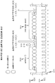
도 8 은 최상위 비트로부터 최하위 비트로 2진 비트들을 3진수들로 변환하는 방법을 예시한다. 3진수의 각각의 디지트는 수신 디바이스에 송신되는 심볼들로 트랜스코딩 (변환) 될 수도 있다. 3진수를 표현하는 T0, T1..., T11 를 갖는 12 디지트 3진수 (802) 에 대해, T0 는 30 디지트를 표현하고 (그리고 최하위 디지트이고), 한편 T11 은 311 디지트를 표현한다 (그리고 최상위 디지트이다). 수신된 비트들 (예를 들어, 20 비트 시퀀스) 로 시작하여, 3진수 (802) 의 최상위 디지트 (T11) 가 먼저 얻어진다. 그 후, 다음 최상위 디지트 (T10) 가 다음으로 얻어진다. 이 프로세스는 최하위 디지트 (T0) 가 얻어질 때까지 계속된다. 3진수 (802) 의 디지트 각각은 또한 "트랜지션 넘버"로서 지칭될 수도 있다.8 illustrates a method of converting binary bits to trinary numbers from the most significant bit to the least significant bit. Each digit of the ternary number may be transcoded (transformed) into symbols that are transmitted to the receiving device. For a 12-digit ternary number (802) with T0, T1 ..., T11 representing a ternary number, T0 represents a 3 0 digit (and is the least significant digit), while T11 represents 3 11 digits And the highest digit). Beginning with the received bits (e.g. a 20 bit sequence), the most significant digit T11 of the
도 9 는 최상위 비트로부터 최하위 비트로 2진 비트들을 3진수들로 변환하기 위한 송신기측 로직 회로를 예시한다. 도 8 및 도 9 는 T11, T10, T9, ..., T0 의 순서로 전송되고 있는 12 디지트 3진수 (802) 를 예시한다. 최상위 비트를 먼저 얻어 전송함으로써, 수반되는 로직 및 회로부가 복잡도에 있어서 간략화된다. 도 8 및 도 9에서의 접근 방식에서, 최상위 순차적 심볼이 수신 디바이스에 먼저 송신되고, 이에 따라 MSS 퍼스트 (최상위 심볼 퍼스트) 로 불려진다. 여기에 이용된 "최하위 심볼" 은 3진수 (802) 의 최하위 디지트에 대응하는 트랜스코딩된 심볼을 지칭한다. 도 6 및 도 7 을 참조하여 예를 들면, T0 는 최하위 3진수로부터 기원하기 때문에, T0 가 최하위 심볼인 순차적 심볼로 트랜스코딩된다. 이와 유사하게, 이용된 "최상위 심볼" 은 3진수 (802) 의 최상위 디지트에 대응하는 트랜스코딩된 심볼을 지칭한다. 도 6 및 도 7 을 참조하여 예를 들면, T0 는 최상위 3진수로부터 기원하기 때문에, T11 가 최상위 심볼인 순차적 심볼로 트랜스코딩된다. 그리고, 심볼 투 트랜지션 넘버 컨버터 블록 (530)(도 5) 이 후속하여 트랜스코딩된 (순차적) 심볼을 수신하고 트랜지션 넘버, 즉, 3진수의 디지트로 변환할 때, 이는 최상위 디지트 T11 가 가장 첫번째이고 최하위 디지트 T0 마지막이 될 것이다.Figure 9 illustrates a transmitter side logic circuit for converting binary bits to most significant bits from the most significant bit to the least significant bit. Figures 8 and 9 illustrate a 12-digit
도 5 를 다시 참조하여 보면, 12 비트들의 오리지널 데이터는 역순서로 3진수로 변환되고 (즉, 최상위 비트가 컨버터에 첫번째로 공급되고) 그 후, 3진수의 각각의 디지트 (예를 들어, 각각의 트랜지션 넘버) 가 순차적 심볼로 역순서로 변환 (즉, 트랜스코딩) 되고 이들 트랜스코딩된 심볼들은 역순서로 (즉, 최상위 심볼이 첫번째로) 버스 상에 송신된다.5, the 12-bit original data is converted to a ternary number in reverse order (i.e., the most significant bit is first fed to the converter) and then each digit of the ternary number (e.g., Transition numbers) are transformed (i.e., transcoded) into sequential symbols in reverse order, and these transcoded symbols are transmitted in reverse order (i.e., the most significant symbol first) on the bus.
도 10 은 최상위 비트로부터 최하위 비트로 3진수들을 2진 비트들로 변환하기 위한 방법을 예시한다. 즉, 이 수신기 측 변환은 도 8 및 도 9 에서 예시된 송신기측 변환에서 수행된 동작들과 반대로 된다. 수신 디바이스 (예를 들어, 슬레이브 디바이스) 는 역순서의 송신물을 수신하고 클록 복구 및 심볼 샘플링을 수행하여, 트랜스코딩된 심볼들을 다시 3진수로 변환하며, 이 3진수는 그 후, 3진수를 20 비트 2진 오리지널 데이터로 다시 변환하는 수신기측 로직 회로에 역순서로 공급된다.10 illustrates a method for transforming trinary numbers from the most significant bit to the least significant bit into binary bits. That is, this receiver-side conversion is the opposite of the operations performed in the transmitter-side conversion illustrated in Figs. The receiving device (e. G., A slave device) receives the reverse order of the transmission and performs clock recovery and symbol sampling to convert the transcoded symbols back to a ternary number, Side logic circuits that convert back to 20-bit binary original data.
도 11 은 12 디지트 3진수를 20 비트들로 변환하는 수신기측 로직 회로를 예시한다. 즉, 도 5 를 다시 참조하여 보면, 12 비트들의 오리지널 데이터는 역순서로 3진수로 변환되고 (즉, 최상위 비트가 컨버터에 첫번째로 공급되고) 그 후, 이 트랜지션 넘버는 순차적 심볼들로 역순서로 다시 변환 (즉, 트랜스코딩) 되고 이들 트랜스코딩된 심볼들은 역순서로 버스 상에 송신된다. 수신 디바이스 (예를 들어, 슬레이브 디바이스) 는 역순서의 송신물을 수신하고 클록 복구 및 심볼 샘플링을 수행하여, 트랜스코딩된 심볼들을 다시 3진수로 변환하며, 이 3진수는 그 후, 3진수를 20 비트 2진 오리지널 데이터로 다시 변환하는 도 11 의 로직 회로에 역순서로 공급된다.Figure 11 illustrates a receiver side logic circuit that converts a 12 digit triplet to 20 bits. 5, the 12-bit original data is converted to a ternary number in reverse order (i.e., the most significant bit is first supplied to the converter), and then the transition number is sequentially (I.e., transcoded) and these transcoded symbols are transmitted on the bus in reverse order. The receiving device (e. G., A slave device) receives the reverse order of the transmission and performs clock recovery and symbol sampling to convert the transcoded symbols back to a ternary number, Are supplied in reverse order to the logic circuit of Fig. 11 that converts back to 20-bit binary original data.
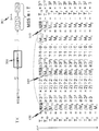
도 12 는 비트 19 (즉, 비트 카운트가 비트 0 인 제 1 비트에서 시작할 때 제 20 비트) 가 CCIe 프로토콜에는 주로 미사용되고 공유 버스 상에서 디바이스들 사이의 커맨드들에 이용될 수도 있는 방법을 개념적으로 예시한다. 즉, 본원에 설명된 인코딩 방식의 결과로서, 엑스트라 비트 (즉, 비트 19) 는 이때 송신된 심볼들에서 이용가능하다. 보다 구체적으로, 도 12 는 비트 19 (즉, 제 20 비트) 를 예시한다. 즉, 컴퓨터 과학에서 통상적인 바와 같이, 비트와이즈 (bit wise) 를 카운팅하는 것은 0 에서 시작하고 비트 19 는 제 20 비트이다. 여기에서, 비트들 0-18 은 0000_0000_00003 내지 2221_2201_20013 의 3진수 범위 내에서 표현된다. 2221_2201_20023 내지 2222_2222_22223 의 범위에서의 3진수들은 미사용된다. 그 결과, 3진수 범위 2221_2201_20023 내지 2222_2222_22223 은 비트 19 (즉, 제 20 비트) 를 표현하는데 이용될 수도 있다. 즉, 2221_2201_20023 3진수는 10,000,000,000,000,000,000 2진수 (0x80000 16진법) 이고 2222_2222_22223 3진수 (0x81BF0) 는 최대 12 디지트 3진수가 가능하다.
Figure 12 conceptually illustrates how a bit 19 (i.e., the twentieth bit when the bit count starts at bit one) is largely unused in the CCIe protocol and may be used for commands between devices on a shared bus do. That is, as a result of the encoding scheme described herein, an extra bit (i.e., bit 19) is available at this time on the transmitted symbols. More specifically, Fig. 12 illustrates bit 19 (i.e., the twentieth bit). That is, counting bit wise starts at 0 and
CCIe 모드에 대한 예시적인 프로토콜Exemplary protocols for CCIe mode
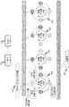
도 13 은 공유 버스가 I2C 모드로부터 CCIe 모드로 동작하도록 스위칭됨을 슬레이브 디바이스들에 표시하기 위해 공유 버스를 통하여 마스터 디바이스에 의해 전송될 수도 있는 CCIe 모드 엔트리 표시자에 대한 예시적인 일반 호출을 예시한다. 일반 호출 (1302) 은 I2C 마스터 디바이스에 의해 공유 버스를 통하여 (예를 들어, 도 3 에서의 마스터 디바이스 (312) 이지만, I2C 모드에 있기는 하지만 SDA 라인 및 SCL 라인을 통하여) 발행되어, I2C 모드로부터 CCIe 모드로의 트랜지션을 모든 I2C-호환가능 디바이스들에 표시할 수도 있다.Figure 13 illustrates an exemplary general call to a CCIe mode entry indicator that may be sent by the master device over the shared bus to indicate to the slave devices that the shared bus is switched to operate in the I2C mode to the CCIe mode. The
I2C 모드에서, CCIe 마스터 디바이스는 "CCIe 모드" 바이트 또는 표시자 (1304) 를 이용하여 이 I2C 일반 호출 (1302) 을 발행한다. CCIe-호환가능 슬레이브 디바이스들은 일반 호출 (1302) 의 수신을 확인응답한다. CCIe-호환가능 슬레이브 디바이스들은 필요에 따라 일반 호출 동안에 (도 3 에서의 제어 데이터 버스 (308) 의) SCL 라인을 로우로 유지함으로써 대기 사이클들을 삽입할 수 있다.In I2C mode, the CCIe master device issues this I2C
일단 CCIe 모드에서는, 모든 CCIe-호환가능 디바이스들은 CCIe 마스터 디바이스로부터의 요청들에 응답가능하다. CCIe 모드를 지원하지 않는 공유된 제어 데이터 버스 상에서의 레거시 I2C-호환가능 슬레이브 디바이스들의 동작적인 상태들 또는 임의의 기능들은 어떠한 CCIe 트랜잭션들에 의해서도 영향을 받지 않는다.Once in CCIe mode, all CCIe-compatible devices are able to respond to requests from the CCIe master device. The operational states or any functions of legacy I2C-compatible slave devices on a shared control data bus that do not support CCIe mode are not affected by any CCIe transactions.
도 14 는 CCIe 모드로부터 I2C 모드로의 트랜지션을 모든 CCIe 에이블 디바이스들에 표시하기 위해 CCIe 마스터 디바이스 (예를 들어, I2C 모드에 있기는 하지만 도 3 에서의 마스터 디바이스 (312)) 에 의해 발행될 수도 있는 예시적인 CCIe 호출 (1402) 을 예시한다. CCIe 마스터 디바이스는 CCIe SID 를 대신하여 이 종료 호출 (1402) 을 발행할 수도 있다.Figure 14 may be issued by a CCIe master device (e.g., in the I2C mode, but the
CCIe 모드에서, CCIe 모드에서의 마지막 데이터에 S 가 후속한 후, CCIe 마스터는 특수 CCIe SID 코드인 "종료" 코드/표시자 (1404) 를 전송하여 (예를 들어, CCIe-호환가능 디바이스들에 대해) CCIe 모드의 종료 및 I2C 모드로의 트랜지션 백을 표시한다. 추가로, "종료" 코드/표시자 (1404) 이후에, CCIe 마스터 디바이스는 S (시작 비트) 를 전송하고, I2C 프로토콜 내에서 제 2 바이트에서 "종료" 코드 (1408) 와 함께 I2C 프로토콜에 따라 "일반 호출" (1406) 이 후속한다. 모든 CCIe 가능 슬레이브들은 일반 호출 (1404) 에 확인응답해야 한다.In CCIe mode, after S is followed by the last data in CCIe mode, the CCIe master sends an "exit" code /
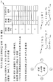
도 15 는 예시적인 CCIe 슬레이브 식별자 (SID) 워드 포맷을 예시한다. 이는 CCIe SID 워드 포맷 (1502) 의 부분으로서 16-비트 슬레이브 식별자 (SID)(1504) 의 사용을 예시한다. 이러한 SID 워드 포맷은 제어 데이터 버스 상에 워드가 위치할 때 특정 슬레이브 디바이스를 식별하는데 이용된다.15 illustrates an exemplary CCIe slave identifier (SID) word format. This illustrates the use of a 16-bit slave identifier (SID) 1504 as part of the CCIe
도 16 은 예시적인 CCIe 어드레스 워드 포맷 (1602) 을 예시한다. 이는 각각의 어드레스 워드 (1606) 가 16-비트 어드레스 (1604) 를 포함함을 예시한다. 어드레스 워드 (1606) 는 또한 2-비트 제어 코드 (1608) 및 1-비트 에러 검출 상수 (1610) 를 포함한다. 테이블 (1612) 은 제어 코드에 대한 여러 가능한 값들을 예시한다.FIG. 16 illustrates an exemplary CCIe
다수의 어드레스 워드들이 순차적으로 전송될 수도 있다. 현재 제어 코드가 '00'이면, 이는 어드레스 어드가 후속할 것임을 의미한다. 제어 코드가 '01' 이면, 다음 데이터 워드는 기록 데이터 워드이다. 제어 코드가 '01' 이면, 다음 데이터 워드는 판독 사양 워드이다. 제어 코드가 '11'이면 금지된다.Multiple address words may be transmitted sequentially. If the current control code is '00', this means that the address ad will follow. If the control code is '01', the next data word is a write data word. If the control code is '01', the next data word is the read specification word. If the control code is '11', it is prohibited.
도 17 은 예시적인 기록 데이터 워드 포맷 (1702) 을 예시한다. 이는 각각의 기록 데이터 워드 (1700) 가 16-비트 기록 데이터 부분 (1702) 을 포함함을 예시한다. 기록 데이터 워드 (1700) 는 또한 2-비트 제어 코드 (1704) 및 1 비트 에러 검출 상수 (1710) 를 포함한다. 테이블 (1714) 은 제어 코드에 대한 여러 가능한 값들을 예시한다.FIG. 17 illustrates an exemplary write data word format 1702. FIG. This illustrates that each
다수의 기록 데이터 워드들이 순차적으로 전송될 수 있다. 현재 기록 워드의 제어 코드가 '00' (심볼 C0) 이면, 데이터는 이전 어드레스에 기록될 것이다. 현재 기록 워드의 제어 코드가 '01' (심볼 C1) 이면, 데이터는 이전 어드레스+1 에 기록될 것이다. 제어 코드가 '10' (심볼 E) 이면, 다음 워드는 SID 또는 종료 코드일 것이다.A plurality of write data words may be sequentially transmitted. If the control code of the current write word is '00' (symbol C0), the data will be written to the previous address. If the control code of the current write word is '01' (symbol C1), the data will be written to the previous address + 1. If the control code is '10' (symbol E), then the next word will be the SID or exit code.
도 18 은 예시적인 판독 사양 워드 포맷 (1800) 을 예시한다. 판독 사양 데이터 워드 (1800) 는 16 비트 판독 데이터 값 부분 (1804), 2 비트 제어 코드 (1808) 및 3 비트 에러 검출 상수 (1810) 를 포함할 수도 있다.FIG. 18 illustrates an exemplary read
마지막 어드레스 워드 (1807) 이후에 "판독 spec" (RS) 워드 (1812) 가 후속한다. 판독 spec (RS) 워드 (1812) 는 다음에 오는 판독 데이터 워드들의 넘버를 특정한다. 테이블 (1816) 에 예시된 바와 같이, 제어 코드 '00' 는 동일한 어드레스로부터의 판독 워드를 표시하는데 이용된다. 제어 코드 '01' 는 증분 어드레스로부터의 판독 워드들을 표시하는데 이용된다. (데이터가 판독되고 있는) 슬레이브 디바이스는 "판독 spec" (RS) 워드 (1804) 에 의해 특정된 것보다 더 많은 데이터 워드들 (CHK 워드들을 포함하지 않음) 을 전송하지 않는다. 슬레이브 디바이스는 (CHK 워드를 포함하는 않는) 적어도 하나의 판독 워드를 전송한다. 슬레이브 디바이스는 "판독 spec" (RS) 워드 (1804) 에 의해 특정된 워드들의 넘버를 전송하기 전에 판독 트랜스퍼를 종료할 수도 있다.Followed by a "read spec" (RS)
도 19 는 예시적인 판독 데이터 워드 포맷 (1902) 을 예시한다. 판독 데이터 워드 (1902) 는 16 비트 판독 데이터 값 부분 (1904), 2 비트 제어 코드 (1906) 및 1 비트 에러 검출 상수 (1908) 를 포함할 수도 있다. SID (1907) 에 의해 어드레싱된 슬레이브 디바이스는 워드들의 넘버를 결정하여 요청한 마스터 디바이스에 리턴시킨다. 테이블 (1916) 에 예시된 바와 같이, 판독 워드가 동일한 어드레스로부터 계속되면, 제어 코드는 '00' (심볼 R0) 이다. 판독 워드가 증분 어드레스로부터 계속되면, 제어 코드는 '01' (심볼 R1) 이다. 워드가 마지막 판독 워드이고 그 후 CHK 가 없다면, 제어 코드는 "10"(심볼 E) 이다. 제어 코드가 '00'이면 금지된다.
FIG. 19 illustrates an exemplary read
공유된 버스를 통한 예시적인 I2C 송신들 대 CCIe 송신들Exemplary I2C transmissions over the shared bus to CCIe transmissions
도 20 은 I2C 1 바이트 기록 데이터 동작의 예시적인 타이밍도를 예시한다. 이 예에서, 공유된 제어 데이터 버스 (예를 들어, 도 3 에서의 제어 데이터 버스 (308)) 는 시리얼 데이터 라인 (SDA; 2002) 및 시리얼 클록 라인 (SCL; 2004) 을 포함한다. 도 20 에 예시된 송신 방식은 "I2C" 모드로서 지칭될 수도 있다. SCL 라인 (2004) 은 마스터 디바이스로부터 모든 슬레이브 디바이스들로 클록을 전송하는데 이용되는 한편, SDA 라인 (2002) 은 데이터 비트들을 송신한다. I2C 마스터 디바이스는 7-비트 슬레이브 ID (2008) 를 SDA 라인 (2002) 에서 전송하여 I2C 버스 상의 어느 슬레이브 디바이스가 마스터 디바이스가 액세스하기를 원하는 슬레이브 디바이스인지를 표시하고, 그 후, 기록 동작을 표시하는 1 비트를 전송한다. 그 ID 가 7-비트 슬레이브 ID (2008) 와 매칭하는 슬레이브 디바이스만이 의도된 액션들을 야기할 수 있다. I2C 슬레이브 디바이스가 자기 자신의 ID 를 검출하기 위하여, 마스터 디바이스는 SDA 라인 상에서 적어도 8-비트들을 (또는 SCL 라인 상에서 8 클록 펄스들을) 전송해야 한다.Figure 20 illustrates an exemplary timing diagram of I2C 1-byte write data operation. In this example, a shared control data bus (e.g.,
I2C 표준은, 모든 I2C 호환가능 슬레이브 디바이스들이 (예를 들어, SCL 라인이 하이이기는 하지만 SDA 라인 상에서 하이-투-로우 트랜지션으로 표시되는) START 조건 (2006) 의 수신시에 자신들의 버스 로직을 리셋하는 것을 요구한다.The I2C standard allows all I2C compatible slave devices to reset their bus logic upon receipt of a START condition 2006 (e.g., the SCL line is high, but displayed as a high-to-low transition on the SDA line) .
CCIe 프로토콜은 데이터 송신물 내에 클록 신호를 임베딩한 상태에서 데이터 송신물에 대해 SDA 라인 (2002) 과 SCL 라인 (2004) 양쪽 모두를 이용한다. 예를 들어, 데이터 비트들은 복수의 심볼들로 트랜스코딩될 수도 있고, 그 후, 이 심볼들은 라인들을 통하여 송신된다. 클록 신호 (도 20 에서 I2C 버스에 대해 SCL 라인) 를 심볼 트랜지션들 내에 임베딩함으로써 SDA 라인 (2002) 과 SCL 라인 (2004) 양쪽 모두가 데이터 송신을 위하여 이용될 수도 있다.The CCIe protocol uses both
도 21 은 데이터 비트들이 SDA 라인 (2102) 및 SCL 라인 (2104) 을 통한 송신에 대하여 12 개의 심볼들로 트랜스코딩된 예시적인 CCIe 송신을 예시한다. 도 21 에 예시된 송신 방식은 "CCIe" 모드로서 지칭될 수도 있다. CCIe 모드는 푸시-풀 드라이버들에 의해 구동되는 소스 동기식이다. 무엇이 데이터를 공유된 제어 데이터 버스를 통해 발송하든 간에, 데이터에 임베딩된 클록 정보를 (예를 들어, 심볼-투-심볼 트랜지션들 내에서) 발송한다. 결과적으로, 제어 데이터 버스 상에서 오직 하나의 디바이스만이 언제든지 공유 제어 데이터 버스를 구동시키도록 허용된다.FIG. 21 illustrates an exemplary CCIe transmission in which data bits are transcoded into 12 symbols for transmission over
레거시 I2C 디바이스들과 CCIe 디바이스들 양쪽 모두를 동일한 버스를 통하여 지원하기 위하여, CCIe 모드 동작들은 동일한 START 조건 (2106, 2108, 2110) 을 이용하며, 이는 레거시 I2C 슬레이브 디바이스들이 어떠한 CCIe 동작들과 작용하는 것을 방지한다 (예를 들어, CCIe 모드 동안에 시작 조건은 레거시 I2C 슬레이브 디바이스들로 하여금 리셋하게 한다). 이 예에서, START 조건 (2106, 2108, 2110)(즉, SCL 라인 (2104) 이 하이이지만, SDA 라인 (2102) 상에서 하이-투-로우 트랜지션으로 표시됨) 은 풀 슬레이브 ID (즉, 풀 7 비트들) 가 송신되기 전에 검출되고 이에 따라 이는 (7 비트들보다 작은) 불완전한 슬레이브 ID 이다. 마스터 디바이스가 6 개의 SCL 펄스들을 전송한 다음 START 조건 (2106, 2108, 2110) 을 발행하면, 모든 레거시 I2C 슬레이브 디바이스들은 데이터를 I2C Slave ID 로서 인식하기 전에 자신들의 버스 로직을 리셋한다. (예를 들어, 매 2 개의 심볼들에 대응하는) 6-비트 시퀀스들은 2 개의 START 조건들 (2106, 2108, 2110) 사이에서 전송되기 때문에, 이들 6-비트 시퀀스들은 어떠한 I2C 슬레이브 디바이스에 의해서도 유효 슬레이브 ID 로서 디코딩되지 않는다. 그 결과, 레거시 I2C 슬레이브 디바이스들은 불완전 슬레이브 ID들에 대해 작용하지 않는다.In order to support both legacy I2C devices and CCIe devices on the same bus, CCIe mode operations use the same START conditions (2106, 2108, 2110), which allows legacy I2C slave devices to operate with any CCIe operations (E.g., the start condition during the CCIe mode causes the legacy I2C slave devices to reset). In this example, the
이 시스템에서, 마스터 디바이스는 버스에 대한 액세스를 제어한다. 따라서, 제어 데이터 버스를 통하여 송신하기를 희망하는 임의의 디바이스는 예를 들어, 인터럽트 요청을 발행함으로써, 마스터 디바이스에게 이러한 액세스에 대해 요청해야 한다. 인터럽트들을 발행하는 이전 메카니즘들은 전용 인터럽트들 라인들 또는 전용 인터럽트 버스에 의존하였다. 그러나, 이러한 전용 인터럽트 라인들 또는 버스는 디바이스들이 이러한 인터럽트 라인 또는 버스를 수용하기 위해 적어도 하나의 추가적인 핀을 포함해야 함을 의미한다. 이러한 전용 인터럽트 핀 및 라인들/버스들의 요구를 제거하기 위해, CCIe 내에서의 대역내 인터럽트들에 대한 메카니즘이 요구된다.In this system, the master device controls access to the bus. Thus, any device wishing to transmit via the control data bus must request such access to the master device, for example, by issuing an interrupt request. Previous mechanisms for issuing interrupts relied on dedicated interrupts lines or dedicated interrupt buses. However, these dedicated interrupt lines or buses mean that the devices must include at least one additional pin to accommodate such an interrupt line or bus. To eliminate the need for these dedicated interrupt pins and lines / busses, a mechanism for in-band interrupts within CCIe is required.
대역내 인터럽트들의 이용은 또한 버스 경합 또는 충돌을 회피시킨다. 예를 들어, 충돌을 방지하기 위해, 마스터 디바이스가 제어 데이터 버스를 구동시키는 동안에, 슬레이브 디바이스는 IRQ 를 표명하도록 제어 데이터 버스 (예를 들어, SDA 라인 (2102) 또는 SCL 라인 (2104)) 를 구동하는 것이 허용되지 않아야 한다.
The use of in-band interrupts also avoids bus contention or collision. For example, to prevent collisions, while the master device drives the control data bus, the slave device drives a control data bus (e.g.,
예시적인 비트 19 영역 및 체크섬
도 22 는 본원에 예시된 인코딩 방식으로부터 야기되는 제 20 비트 (비트 19) 의 예시적인 맵핑을 예시한다. 알 수 있는 바와 같이, 이용가능한 3진수들은 마스터 디바이스들과 슬레이브 디바이스들 사이에서 피쳐들 및 능력들을 확장하도록 서브할 수도 있다. 예를 들어, 비트 19 내에서 이용가능한 이 3진수 공간 (즉, 비트 19 가 '1' 인 데이터 영역) 은 (a) 슬레이브 투 슬레이브 송신들, (b) 송신들에 대한 체크섬, (c) 슬레이브 디바이스들에 대한 마스터 동작 핸드오버, (d) 하트비트 클록 등을 표시 또는 실시하도록 서브할 수도 있다.22 illustrates an exemplary mapping of the twentieth bit (bit 19) resulting from the encoding scheme illustrated herein. As can be appreciated, available ternary numbers may serve to extend features and capabilities between master devices and slave devices. For example, this ternary space available in bit 19 (i.e., the data area with
도 23 은 도 22 의 제 20 비트 (비트 19) 의 예시적인 맵핑 내에서의 서브영역의 세부사항들을 예시한다.FIG. 23 illustrates the details of the sub-region within the exemplary mapping of the twentieth bit (bit 19) of FIG.
도 24 는 발생할 수도 있는 여러 심볼 에러 조건들을 예시한다. 타이밍도 (2402) 는 제어 데이터 버스 (SDA 라인 및 SCL 라인) 와 수신기 클록 (RXCLK) 을 통한 정확한 송신을 예시한다.Figure 24 illustrates several symbol error conditions that may occur. Timing diagram 2402 illustrates accurate transmission over the control data bus (SDA line and SCL line) and receiver clock (RXCLK).
클록 미스 (2404) 는 수신기 클록 (RXCLK) 이 2 개의 사이클들 (2412 및 2414) 을 손실하여 데이터 비트 (2410) 가 부정확하게 검출되게 되는 것을 예시한다. 더 많은 후속하는 워드들이 동일한 트랜스퍼 방향으로 존재하면, 워드 데이터 에러들이 후속하는 다음 워드들에서 검출되기 더 쉽게 된다. 동기화 (SYNC) 손실이 또한 검출될 수도 있다. 에러가 마지막 워드에서 발생하면, 마스터 디바이스는 타임아웃 검출 기능을 필요로 한다.
엑스트라 클록 (2406) 은 수신기 클록 (RXCLK) 이 엑스트라 클록 사이클 (2420) 에서 검출된 엑스트라 심볼 '01' (2416 및 2418) 을 갖는 경우에 예시된다. 이 에러는 워드 또는 다음에 오는 워드들에서 더 검출되기 쉽다. 동기화 손실이 또한 검출될 수도 있다.The
심볼 에러 (2408) 는 수신기 클록 (RXCLK) 손실들이 존재하지 않지만 단일의 심볼 에러 (2422) 가 발생하는 경우에 예시된다. 이 에러는 워드 또는 다음에 오는 워드들에서 더 검출되기 쉽다. 체크섬 에러가 더 검출되기 쉽게 된다.
송신된 심볼들 내에서의 예시적인 에러 검출Exemplary error detection within transmitted symbols
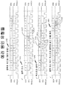
도 25 내지 도 30 은 여러 CCIe 워드들에 대하여 발생할 수도 있는 여러 심볼 에러 조건들 (즉, 심볼 슬립이 없는 단일 심볼 에러) 를 예시한다. 도시된 바와 같이, 이들 에러들은 아래에 추가로 설명될 바와 같이, 3 개의 비트들 (비트 0, 1 및 2) 를 이용하여 검출될 수도 있다. 이들 예들은 세 (3) 개의 최하위 비트들 (Bits [2:0]) 을 에러 검출을 위해 이용한다.Figures 25-30 illustrate several symbol error conditions (i.e., a single symbol error without symbol slip) that may occur for multiple CCIe words. As shown, these errors may be detected using three bits (
도 25 는 송신된 심볼 시퀀스 (0321_0321_0321) 에서 가능한 에러들, 및 이러한 에러들이 3 개의 최하위 비트들 내에서 어떻게 검출가능한지의 방법을 나타내는 테이블 (2500) 을 예시한다. (Bits [19:0]) 0000_0000_0000_0000_0000 (2502) 의 12 비트 시퀀스는 3진수 (T11 ... T0) 0000_0000_00003 (2504) 로 변환되고, 이는 이후 도 5, 도 6, 도 7, 도 8, 도 9 및 도 10 에 예시된 방법을 이용하여 순차적 심볼들 (S11 ... S0) 0321_0321_0321 (2506) 로 변환된다. 이 예의 목적들을 위하여, 3 개의 최하위 비트들 (2508) 은 모두 0 이다 (000). 에러가 오리지널의 순차적 심볼들 0321_0321_0321 (2506) 의 심볼들 중 어느 것의 송신 동안에 도입되면, 이들은 에러있는 심볼들 (2510) 을 가져온다. 예를 들어, 마지막 심볼 "1" 이 "0" 으로 변경되면, 이는 "000" 로부터 "010" 로의 3 개의 최하위 비트들의 변화를 가져온다. 마지막 심볼 "1" 이 "3" 으로 변경되면, 이는 "000" 로부터 "001" 로의 3 개의 최하위 비트들의 변화를 가져온다. "1" 의 첫번째 심볼이 "2" 로 변경되면, 이는 "000" 로부터 "100" 로의 3 개의 최하위 비트들의 변화를 가져온다. 테이블 (2500) 은 최하위 비트들이 알려진 상수 (예를 들어, "000"의 고정된 상수) 인 한, 임의의 단일 심볼의 변화가 세 (3) 개의 최하위 비트들에 의해 어떻게 검출가능한지의 방법의 다른 여러 예들을 예시한다.25 illustrates a table 2500 that illustrates possible errors in the transmitted symbol sequence (0321_0321_0321) and how such errors are detectable within the three least significant bits. The 12 bit sequence of bits Bits [19: 0] 0000_0000_0000_0000_0000 2502 is converted into a ternary number (T11 ... T0) 0000_0000_0000 3 (2504), which will be described later with reference to FIGS. 5, 6, 7, (S11 ... S0) 0321_0321_0321 (2506) using the method illustrated in FIG. 9 and FIG. For purposes of this example, the three least
도 26 은 송신된 심볼 시퀀스 (2301_2301_2301) 에서 가능한 에러들, 및 이러한 에러들이 3 개의 최하위 비트들 내에서 어떻게 검출가능한지의 방법을 나타내는 테이블 (2600) 을 예시한다. (Bits [19:0]) 0100_0000_1101_1111_1000 (2602) 의 12 비트 시퀀스는 3진수 (T11 ... T0) 1111_1111_11113 (2604) 로 변환되고, 이는 이후 도 5, 도 6, 도 7, 도 8, 도 9 및 도 10 에 예시된 방법을 이용하여 순차적 심볼들 (S11 ... S0) 2301_2301_2301 (2606) 로 변환된다. 이 예의 목적들을 위하여, 3 개의 최하위 비트들 (2608) 은 모두 0 이다 (000). 에러가 오리지널의 순차적 심볼들 2301_2301_2301 (2606) 의 심볼들 중 어느 것의 송신 동안에 도입되면, 이들은 에러 심볼들 (2610) 을 가져온다. 예를 들어, 마지막 심볼 "1" 이 "3" 으로 변경되면, 이는 "000" 로부터 "111" 로의 3 개의 최하위 비트들의 변화를 가져온다. 마지막 심볼 "1" 이 "2" 로 변경되면, 이는 "000" 로부터 "001" 로의 3 개의 최하위 비트들의 변화를 가져온다. "2" 의 첫번째 심볼이 "0" 으로 변경되면, 이는 "000" 로부터 "100" 으로의 3 개의 최하위 비트들의 변화를 가져온다. 테이블 (2600) 은 3 개의 최하위 비트들이 알려진 상수 (예를 들어, "000"의 고정된 상수) 인 한, 임의의 단일 심볼의 변경이 세 (3) 개의 최하위 비트들에 의해 어떻게 검출가능한지의 방법의 다른 여러 예들을 예시한다.Figure 26 illustrates possible errors in the transmitted symbol sequence 2301_2301_2301 and a table 2600 that shows how these errors can be detected within the three least significant bits. (Bits [19: 0]) The 12-bit sequence of 0100_0000_1101_1111_1000 2602 is converted into a ternary number (T11 ... T0) 1111_1111_1111 3 (2604), which will be described later with reference to FIGS. 5, 6, 7, (S11 ... S0) 2301_2301_2301 (2606) using the method illustrated in FIGS. For purposes of this example, the three least
도 27 은 송신된 심볼 시퀀스 (3131_3131_3131) 에서 가능한 에러들, 및 이러한 에러들이 3 개의 최하위 비트들 내에서 어떻게 검출가능한지의 방법을 나타내는 테이블 (2700) 을 예시한다. (Bits [19:0]) 1000_0001_1011_1111_0000 (2702) 의 12 비트 시퀀스는 3진수 (T11 ... T0) 2222_2222_22223 (2704) 으로 변환되고, 이는 이후 도 5, 도 6, 도 7, 도 8, 도 9 및 도 10 에 예시된 방법을 이용하여 순차적 심볼들 (S11 ... S0) 3131_3131_3131 (2706) 로 변환된다. 이 예의 목적들을 위하여, 3 개의 최하위 비트들 (2708) 은 모두 0 이다 (000). 에러가 오리지널의 순차적 심볼들 3131_3131_3131 (2706) 의 심볼들 중 어느 것의 송신 동안에 도입되면, 이들은 에러 심볼들 (2710) 을 가져온다. 예를 들어, 마지막 심볼 "1" 이 "0" 으로 변경되면, 이는 "000" 로부터 "111" 로의 3 개의 최하위 비트들의 변화를 가져온다. 마지막 심볼 "1" 이 "2" 로 변경되면, 이는 "000" 로부터 "100" 로의 3 개의 최하위 비트들의 변화를 가져온다. "3" 의 첫번째 심볼이 "0" 으로 변경되면, 이는 "000" 로부터 "001" 로의 3 개의 최하위 비트들의 변화를 가져온다. 테이블 (2700) 은 최하위 비트들이 알려진 상수 (예를 들어, "000"의 고정된 상수) 인 한, 임의의 단일 심볼의 변화가 세 (3) 개의 최하위 비트들에 의해 어떻게 검출가능한지의 방법의 다른 여러 예들을 예시한다.Figure 27 illustrates possible errors in the transmitted symbol sequence 3131_3131_3131, and a table 2700 that shows how these errors can be detected within the three least significant bits. (T11 ... T0) 2222_2222_2222 3 (2704), which is then converted into a binary sequence (Bits [19: 0]) 1000_0001_1011_1111_0000 2702, (S11 ... S0) 3131_3131_3131 (2706) using the method illustrated in FIG. 9 and FIG. For purposes of this example, the three least
도 28 은 송신된 심볼 시퀀스 (0132_3101_3231) 에서 가능한 에러들, 및 이러한 에러들이 3 개의 최하위 비트들 내에서 어떻게 검출가능한지의 방법을 나타내는 테이블 (2800) 을 예시한다. (Bits [19:0]) 0001_1000_1111_0011_1000 (2802) 의 12 비트 시퀀스는 3진수 (T11 ... T0) 0120_1201_20123 (2804) 로 변환되고, 이는 이후 도 5, 도 6, 도 7, 도 8, 도 9 및 도 10 에 예시된 방법을 이용하여 순차적 심볼들 (S11 ... S0) 0132_3101_3231 (2806) 로 변환된다. 이 예의 목적들을 위하여, 3 개의 최하위 비트들 (2808) 은 모두 0 이다 (000). 에러가 오리지널의 순차적 심볼들 0132_3101_3231 (2806) 의 심볼들 중 어느 것의 송신 동안에 도입되면, 이들은 에러 심볼들 (2810) 을 가져온다. 예를 들어, 마지막 심볼 "1" 이 "0" 으로 변경되면, 이는 "000" 로부터 "111" 로의 3 개의 최하위 비트들의 변화를 가져온다. 마지막 심볼 "1" 이 "2" 로 변경되면, 이는 "000" 로부터 "110" 로의 3 개의 최하위 비트들의 변화를 가져온다. "0" 의 첫번째 심볼이 "3" 으로 변경되면, 이는 "000" 로부터 "111" 로의 3 개의 최하위 비트들의 변화를 가져온다. 테이블 (2800) 은 3 개의 최하위 비트들이 알려진 상수 (예를 들어, "000"의 고정된 상수) 인 한, 임의의 단일 심볼의 변경이 세 (3) 개의 최하위 비트들에 의해 어떻게 검출가능한지의 방법의 다른 여러 예들을 예시한다.FIG. 28 illustrates possible errors in the transmitted symbol sequence (0132_3101_3231) and a table 2800 that shows how these errors can be detected within the three least significant bits. (Bits [19: 0]) The 12 bit sequence of 0001_1000_1111_0011_1000 2802 is converted into a binary number (T11 ... T0) 0120_1201_2012 3 (2804), which will be described later with reference to Figures 5, 6, 7, (S11 ... S0) 0132_3101_3231 (2806) using the method illustrated in FIG. 9 and FIG. For purposes of this example, the three least
도 29 는 송신된 심볼 시퀀스 (2030_2120_3021) 에서 가능한 에러들, 및 이러한 에러들이 3 개의 최하위 비트들 내에서 어떻게 검출가능한지의 방법을 나타내는 테이블 (2900) 을 예시한다. (Bits [19:0]) 0100_1010_1101_1010_1000 (2902) 의 12 비트 시퀀스는 3진수 (T11 ... T0) 1201_2012_01203 (2904) 로 변환되고, 이는 이후 도 5, 도 6, 도 7, 도 8, 도 9 및 도 10 에 예시된 방법을 이용하여 순차적 심볼들 (S11 ... S0) 2030_2120_3021 (2906) 로 변환된다. 이 예의 목적들을 위하여, 3 개의 최하위 비트들 (2908) 은 모두 0 이다 (000). 에러가 오리지널의 순차적 심볼들 3231_0132_3101 (2906) 의 심볼들 중 어느 것의 송신 동안에 도입되면, 이들은 에러 심볼들 (2910) 을 가져온다. 예를 들어, 마지막 심볼 "1" 이 "0" 으로 변경되면, 이는 "000" 로부터 "010" 로의 3 개의 최하위 비트들의 변화를 가져온다. "2" 의 첫번째 심볼이 "0" 으로 변경되면, 이는 "000" 로부터 "011" 으로의 3 개의 최하위 비트들의 변화를 가져온다. 테이블 (2900) 은 최하위 비트들이 알려진 상수 (예를 들어, "000"의 고정된 상수) 인 한, 임의의 단일 심볼의 변화가 세 (3) 개의 최하위 비트들에 의해 어떻게 검출가능한지의 방법의 다른 여러 예들을 예시한다.29 illustrates a table 2900 that illustrates possible errors in the transmitted symbol sequence 2030_2120_3021, and how such errors are detectable within the three least significant bits. (Bits [19: 0]) The 12 bit sequence of 0100_1010_1101_1010_1000 (2902) is converted into a binary number (T11 ... T0) 1201_2012_0120 3 (2904) (S11 ... S0) 2030_2120_3021 (2906) using the method illustrated in FIG. 9 and FIG. For purposes of this example, the three least
도 30 은 송신된 심볼 시퀀스 (3231_0132_3101) 에서 가능한 에러들, 및 이러한 에러들이 3 개의 최하위 비트들 내에서 어떻게 검출가능한지의 방법을 나타내는 테이블을 예시한다. (Bits [19:0]) 0101_1110_1101_0000_1000 (3002) 의 12 비트 시퀀스는 3진수 (T11 ... T0) 2012_0120_12013 (3004) 로 변환되고, 이는 이후 도 5, 도 6, 도 7, 도 8, 도 9 및 도 10 에 예시된 방법을 이용하여 순차적 심볼들 (S11 ... S0) 3231_0132_3101 (3006) 로 변환된다. 이 예의 목적들을 위하여, 3 개의 최하위 비트들 (3008) 은 모두 0 이다 (000). 에러가 오리지널의 순차적 심볼들 3231_0132_3101 (3006) 의 심볼들 중 어느 것의 송신 동안에 도입되면, 이들은 에러 심볼들 (3010) 을 가져온다. 예를 들어, 마지막 심볼 "1" 이 "3" 으로 변경되면, 이는 "000" 로부터 "111" 로의 3 개의 최하위 비트들의 변화를 가져온다. "3" 의 첫번째 심볼이 "0" 으로 변경되면, 이는 "000" 로부터 "100" 로의 3 개의 최하위 비트들의 변화를 가져온다. 테이블 (3000) 은 최하위 비트들이 알려진 상수 (예를 들어, "000"의 고정된 상수) 인 한, 임의의 단일 심볼의 변화가 세 (3) 개의 최하위 비트들에 의해 어떻게 검출가능한지의 방법의 다른 여러 예들을 예시한다.
Figure 30 illustrates possible errors in the transmitted symbol sequence 3231_0132_3101, and a table showing how these errors can be detected within the three least significant bits. (Bits [19: 0]) 0101_1110_1101_0000_1000 3002 is converted into a binary number (T11 ... T0) 2012_0120_1201 3 (3004), which will be described later with reference to FIGS. 5, 6, 7, 8 (S11 ... S0) 3231_0132_3101 (3006) using the method illustrated in FIG. 9 and FIG. For purposes of this example, the three least
예시적인 마스터/슬레이브 디바이스 구현들Exemplary master / slave device implementations
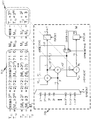
다음 도 31 을 참조하여 보면, 본 개시물에 따라 제공되는 마스터/슬레이브 디바이스의 예시적인 컴포넌트들을 예시하는 블록도가 제공된다. 예시된 바와 같이, 마스터/슬레이브 디바이스 (3114) 는 제어 데이터 버스 (3150) 를 통하여 다른 마스터/슬레이브 디바이스 (3160) 에 커플링된다. 여기에서, 마스터/슬레이브 디바이스들 (3114 또는 3160) 의 어느 것이 여기에 개시된 상술한 양태들에 따라 마스터로서 또는 슬레이브로서 동작할 수도 있고 마스터/슬레이브 디바이스들 (3114 및 3160) 각각은 실질적으로 유사한 컴포넌트들을 가질 수도 있음이 고려된다.31, a block diagram illustrating exemplary components of a master / slave device provided in accordance with the present disclosure is provided. As illustrated, the master /
이 예에서, 마스터/슬레이브 디바이스 (3114) 는 버스 (3102) 로 일반적으로 표현되는 내부 버스 아키텍쳐로 구현될 수도 있다. 버스 (3102) 는 마스터/슬레이브 디바이스 (3114) 의 특정 애플리케이션 및 전체적인 설계 제약들에 의존하여, 임의의 수의 상호접속 버스들 및 브리지들을 포함할 수도 있다. 버스 (3102) 는 (프로세서 (3104) 로 일반적으로 표현되는) 하나 이상의 프로세서들, 메모리 (3105) 및 (컴퓨터 판독가능 매체 (3106) 로 일반적으로 표현되는) 컴퓨터 판독가능 매체들을 포함하는 여러 회로들을 함께 링크시킨다. 버스 (3102) 는 또한 다른 회로들, 예컨대, 타이밍 소스들, 주변기기들, 전압 조절기들, 및 전력 관리 회로들을 링크할 수도 있으며, 이는 공지되어 있으므로, 더 이상 설명되지 않을 것이다.In this example, the master /
특정 구현에서, 제어 데이터 버스 인터페이스 (3108) 는 제어 데이터 버스 (3150) 와 마스터/슬레이브 디바이스 (3114) 사이의 인터페이스를 제공하며, 프로세서 (3104) 는 제어 데이터 버스 (3150) 를 통한 마스터/슬레이브 디바이스 (3114) 와 마스터/슬레이브 디바이스 (3160) 사이의 워드의 인코딩된 통신을 용이하게 하도록 구성된다. 여기에서, 제어 데이터 버스 (3150) 는 2-라인 버스일 수도 있고 인코딩된 통신은 에러 검출 상수를 최대화하는 것을 용이하게 하도록 인코딩된 통신의 복수의 최하위 비트들을 할당하는 프로토콜 (예를 들어,CCIe 프로토콜) 에 따라 인코딩될 수도 있는 것으로 고려된다. 이전에 주지된 바와 같이, 이러한 최대화는 워드의 데이터 부분의 적어도 제 1 최상위 비트 또는 적어도 하나의 추가적인 에러 검출 비트를 포함하기 위해 복수의 최하위 비트들을 할당하는 프로토콜을 통하여 실현될 수도 있다.In a particular implementation, the control
본 개시물의 추가의 양태에서, 컴퓨터 판독가능 매체 (3106) 는 본원에 개시된 바와 같이, 제어 데이터 버스 (3150) 를 통하여 에러 검출 최적화를 용이하게 하는 여러 명령들 (3106a, 3106b, 및/또는 3106c) 을 포함하도록 구성된다. 이와 유사하게, 이러한 양태들은 도시된 바와 같이, 예시된 회로들 (3120, 3130, 및/또는 3140) 의 어느 것에 프로세서 (3104) 를 커플링하는 것에 의해 하드웨어를 통하여 구현되도록 의도될 수 있다. 또한, 제어 데이터 버스 (3150) 를 통한 에러 검출 최적화는 명령들 (3106a, 3106b, 및/또는 3106c) 의 임의의 조합 뿐만 아니라 회로들 (3120, 3130, 및/또는 3140) 의 임의의 조합에 의해 용이하게 될 수도 있음이 고려된다.In a further aspect of the disclosure, the computer readable medium 3106 includes a plurality of
예를 들어, 인코더/디코더 명령들 (3106a) 및 인코더/디코더 회로 (3120) 는 선택된/검출된 프로토콜 (예를 들어, CCIe 프로토콜) 에 따라 인코딩/디코딩 워드들을 향하여 교시된다. 이전에 언급된 바와 같이, 이러한 인코딩/디코딩은 디지트 바이 디지트 기반으로 3진수를 복수의 심볼들로 변환하여 (예를 들어, 12 개의 디지트 3진수는 12 개의 심볼들로 귀결됨), 상술한 "엑스트라 비트"(비트 19) 를 산출하는 것을 포함할 수도 있다.For example, encoder /
본 개시물의 다른 양태에서, 비트 할당 명령들 (3106b) 및 비트 할당 회로 (3130) 가 원하는 워드 포맷 (예를 들어, SID 워드 포맷, 어드레스 워드 포맷, 기록 데이터 워드 포맷, 판독 사용 워드 포맷 또는 판독 데이터 워드 포맷) 에 따라 비트들을 할당하는 것에 대하여 교시된다. 이를 위하여, 본원에 개시된 여러 고려된 워드 포맷들은 20-비트 워드 포맷들을 포함하고, 3 개의 최하위 비트들은 에러검출 상수를 최대화하는 것을 용이하게 하도록 할당된다. 또한, 비트 할당 명령들 (3106b) 및/또는 비트 할당 회로 (3130) 의 어느 것이, 에러 검출 최적화가 요구되는지 또는 데이터 최적화가 요구되는지에 따라 이러한 최대화를 용이하게 하도록 유연성있는 비트 할당 방식을 용이하게 하도록 구성될 수도 있음이 고려된다. 예를 들어, 특정 구현에서, 최하위 비트는 에러 검출을 위해 할당되고, 제 2 최하위 비트 및 제 3 최하위 비트 각각은 워드의 데이터 부분의 추가적인 에러 검출 비트들 또는 2 개의 최상위 비트들에 대해 할당된다.In other aspects of the present disclosure, the
본 개시물의 특정 양태에서, 통신 명령들 (3106c) 및/또는 통신 회로 (3140) 는 제어 데이터 버스 (3150) 와 마스터/슬레이브 디바이스 (3114) 를 인터페이스하도록 구성될 수도 있다. 통신 명령들 (3106c) 및/또는 통신 회로 (3140) 의 어느 것은 본원에 개시된 에러 검출 최적화를 용이하게 하는 프로토콜 (예를 들어, CCIe 프로토콜) 에 따라 마스터/슬레이브 디바이스 (3114) 와 마스터/슬레이브 디바이스 (3160) 사이의 워드의 인코딩된 통신을 용이하게 하도록 구성될 수도 있다.In certain aspects of the disclosure,
도 31 의 나머지 엘리먼트들을 다시 참조하여 보면, 프로세서 (3104) 는 컴퓨터 판독가능 매체 (3106) 상에 저장된 소프트웨어의 실행을 포함한 범용 프로세싱과 버스 (3102) 를 관리하는 것을 담당한다. 프로세서 (3104) 에 의해 실행될 때, 소프트웨어는 마스터/슬레이브 디바이스 (3114) 로 하여금 임의의 특정 장치에 대하여 아래 설명된 여러 기능들을 수행하게 한다. 컴퓨터 판독가능 매체 (3106) 는 또한 소프트웨어를 실행시킬 때 프로세서 (3104) 에 의해 조작되는 데이터를 저장하는데 이용될 수도 있다.Referring again to the remaining elements of FIG. 31,
프로세싱 시스템에서의 하나 이상의 프로세서들 (3104) 은 소프트웨어를 실행할 수도 있다. 소프트웨어는 소프트웨어, 펌웨어, 미들웨어, 마이크로코드, 하드웨어 기술 언어, 또는 그 외의 것으로 지칭되든지 간에, 명령들, 명령 세트들, 데이터, 코드, 코드 세그먼트들, 프로그램 코드, 프로그램들, 서브프로그램들, 소프트웨어 모듈들, 애플리케이션들, 소프트웨어 애플리케이션들, 소프트웨어 패키지들, 루틴들, 서브루틴들, 오브젝트들, 실행가능물들, 실행의 스레드들, 절차들, 기능들 등을 의미하는 것으로 광범위하게 해석되어야 한다. 소프트웨어는 컴퓨터 판독가능 매체 (3106) 상에 상주할 수도 있다. 컴퓨터 판독가능 매체 (3106) 는 비일시적 컴퓨터 판독가능 매체일 수도 있다. 비일시적 컴퓨터 판독가능 매체는 예를 들어, 자기 저장 디바이스 (예를 들어, 하드 디스크, 플로피 디스크, 마그네틱 스트립), 광학 디스크 (예를 들어, 컴팩트 디스크 (CD) 또는 디지털 다기능 디스크 (DVD)), 스마트 카드, 플래시 메모리 디바이스 (예를 들어, 카드, 스틱, 키 드라이브), 랜덤 액세스 메모리 (RAM), 판독 전용 메모리 (ROM), 프로그래밍가능 ROM (PROM), 소거가능 PROM (EPROM), 전기적 소거가능 PROM (EEPROM), 레지스터, 탈착가능 디스크, 및/또는 컴퓨터에 의해 액세스 및 판독될 수도 있는 소프트웨어 및/또는 명령들을 저장하기 위한 임의의 다른 적절한 매체를 포함한다. 컴퓨터 판독가능 매체는 또한 예를 들어, 반송파, 송신 라인, 및 컴퓨터에 의해 액세스 및 판독될 수도 있는 소프트웨어 및/또는 명령들을 송신하기 위한 임의의 다른 적절한 매체를 포함할 수도 있다. 컴퓨터 판독가능 매체 (3106) 는 마스터/슬레이브 디바이스 (3114) 내에, 마스터/슬레이브 디바이스 (3114) 외부에 상주할 수도 있고, 마스터/슬레이브 디바이스 (3114) 를 포함하는 다수의 엔티티들에 걸쳐 분산될 수도 있다. 컴퓨터 판독가능 매체 (3106) 는 컴퓨터 프로그램 제품에서 구현될 수도 있다. 예를 들어, 컴퓨터 프로그램 제품은 패키징 재료들에서 컴퓨터 판독가능 매체를 포함할 수도 있다. 당해 기술 분야의 당업자는 전체 시스템 상에 부여되는 전체 설계 제약들 및 특정 애플리케이션에 따라 본 개시물 전반에 걸쳐 제시된 설명의 기능성을 최상으로 구현하는 방법을 알고 있을 것이다.One or
다음으로 도 32 를 참조하여 보면, 본원에 개시된 양태들에 따라 공유된 버스를 통하여 에러 검출 최적화를 용이하게 하는 예시적인 방법을 예시하는 흐름도가 제공된다. 예시된 바와 같이, 프로세스 (3200) 는 본 사양에 따라 컴퓨팅 디바이스 (예를 들어, 마스터/슬레이브 디바이스 (3114)) 내에서 수행될 수도 있는 일련의 동작들 (acts) 을 포함한다. 예를 들어, 프로세스 (3200) 는 일련의 동작들을 동작들을 구현하는, 컴퓨터 판독가능 저장 매체 상에 저장된 컴퓨터 실행가능 명령들을 실행하는 프로세서를 채용하는 것에 의해 구현될 수도 있다. 다른 실시형태에서, 적어도 하나의 컴퓨터로 하여금 프로세스 (3200) 의 동작들을 구현하게 하기 위한 코드를 포함하는 컴퓨터 판독가능 저장 매체가 고려된다.Referring now to FIG. 32, a flow diagram illustrating an exemplary method for facilitating error detection optimization via a shared bus in accordance with aspects disclosed herein is provided. As illustrated,
예시된 바와 같이, 프로세스 (3200) 는 동작 3210 에서 슬레이브 디바이스에 마스터 디바이스를 커플링하는 것으로 시작한다. 여기에서, 이러한 커플링은 제어 데이터 버스를 통하여 마스터와 슬레이브 디바이스들을 접속하는 것을 포함할 수도 있음을 알아야 한다. 프로세스 (3200) 는 그 후, 동작 3220 으로 진행하며, 여기에서, 제어 데이터 버스를 통한 마스터와 슬레이브 디바이스들 사이의 워드의 인코딩된 통신이 용이하게 된다 (예를 들어, 원하는 프로토콜, 원하는 워드 포맷 등을 선택하는 것). 여기에서, 인코딩된 통신은 워드의 데이터 부분의 적어도 제 1 최상위 비트 또는 적어도 하나의 추가적인 에러 검출 비트를 포함하도록 복수의 최하위 비트들을 할당하는 것에 의해, 인코딩된 통신의 복수의 최하위 비트들을 할당하여 에러 검출 상수를 최대화하는 것을 용이하게 하는 프로토콜에 따라 인코딩되는 것으로 고려된다. 인코딩 및 디코딩 양태들 양자가 고려되기 때문에, 프로세스 (3200) 는 동작 3230 에서, 디코더 동작으로 진행할지 또는 인코더 동작으로 진행할지를 결정하는 것을 더 포함할 수도 있다. 예를 들어, 인코더로서 동작할 때, 프로세스 (3200) 는, 워드들이 본 개시물의 양태들에 따라 에러 검출 상수를 최대화하는 것을 용이하게 하도록 인코딩된 통신의 복수의 최하위 비트들을 할당하는 프로토콜 (예를 들어,CCIe 프로토콜) 에 따라 인코딩되는 동작 3240 으로 진행할 수도 있으며, 후속하여, 인코딩된 통신이 제어 데이터 버스를 통하여 송신되는 동작 3242 에서 종료할 수도 있다. 그렇지 않고 디코더로서 동작하면, 프로세스 (3200) 는, 인코딩된 통신이 제어 데이터 버스를 통하여 수신되는 동작 3250 으로 진행할 수도 있고, 후속하여, 인코딩된 통신이 본원에 개시된 에러 검출 최적화를 용이하게 하는 프로토콜 (예를 들어, CCIe 프로토콜) 에 따라 디코딩되는 동작 3252 에서 종료할 수도 있다.
As illustrated, the
예시적인 인코더 구현들Exemplary encoder implementations
도 31 을 다시 참조하여 보면, 이하 마스터/슬레이브 디바이스 (3114) 를 인코더로서 구성하는 환경에서 예시적인 구현들이 논의된다. 이러한 구현을 위하여, 인코더/디코더 회로 (3120) 가 인코더 회로로서 구성될 수도 있고, 인코더/디코더 명령들 (3106a) 이 인코더 명령들로서 구성될 수도 있는 것으로 고려된다. 이를 위하여, 도 33 에 예시된 바와 같이, 인코더 회로 (3120) 및 인코더 명령들 (3106a) 각각이 복수의 서브컴포넌트들의 어느 것을 통하여 본원에 개시된 양태들에 따라 워드들의 인코딩을 용이하게 하도록 구성될 수도 있는 것으로 또한 고려된다. 즉, 도 33 에 예시된 바와 같이, 인코더 회로 (3120) 는 프로토콜 서브회로 (3310), 최적화 서브회로 (3320), 및 인코딩 서브 회로 (3330) 를 포함할 수도 있는 한편, 인코더 명령들 (3106a) 은 프로토콜 명령들 (3312), 최적화 명령들 (3322) 및 인코딩 명령들 (3332) 을 포함할 수도 있다. 이 특정 구현을 위하여, 비트 할당 회로 (3130) 및 비트 할당 명령들 (3106b) 각각은 비트 할당 방식에 따라 비트들을 할당하는 것에 대하여 지시되며, 여기에서, 비트 할당 방식은 에러 검출 상수를 최대화하는 것을 용이하게 하기 위해 인코딩된 통신의 복수의 최하위 비트들을 할당한다. 그 후, 각각의 프로토콜 서브회로 (3310) 및 프로토콜 명령들 (3312) 은 원하는 프로토콜 (예를 들어, CCIe 프로토콜) 과 연관된 워드의 워드 포맷을 결정하는 것에 대하여 지시되는 한편, 인코딩 서브회로 (3330) 및 인코딩 명령들 (3332) 의 각각은 (예를 들어, 심볼들로 트랜스코딩된 인코딩된 3진수들로서 워드들을 인코딩하는 것에 의해) 인코딩된 통신을 생성하도록 상술한 워드 포맷 및 비트 할당 방식에 따라 워드들을 인코딩하는 것에 대하여 지시된다. 워드들이 인코딩되면, 통신 회로 (3140) 및/또는 통신 명령들 (3106c) 의 어느 것은 제어 데이터 버스를 통하여 인코딩된 통신을 송신하는데 이용될 수도 있다.Referring again to FIG. 31, exemplary implementations are discussed in the context of configuring master /
본 개시물의 추가의 양태에서, 최적화 서브회로 (3320) 및/또는 최적화 명령들 (3322) 의 어느 것이 원하는 워드 포맷 및 대응하는 비트 할당 방식을 통하여 구현할 최적화를 확인하도록 구성될 수도 있는 것으로 고려된다. 특정 구현에서, 최적화 서브회로 (3320) 및/또는 최적화 명령들 (3322) 은 제 1 비트 할당 방식을 갖는 에러 검출 최적화에 따른 워드들의 인코딩과, 제 2 비트 할당 방식을 갖는 데이터 최적화에 따른 워드들의 인코딩 사이의 스위칭을 용이하게 하도록 구성될 수도 있다. 예를 들어, 에러 검출 최적화가 데이터 최적화보다 선호되면, 인코딩 서브회로 (3330) 및/또는 인코딩 명령들 (3332) 은 에러 검출 최적화에 따라 워드들을 인코딩하도록 구성될 수도 있고, 여기에서, 복수의 최하위 비트들은 고정된 수의 3 비트들 (예를 들어, 3 개의 최하위 비트들) 을 포함하며, 비트 할당 회로 (3130) 및/또는 비트 할당 명령들 (3106b) 은 에러 검출을 위하여 최하위 비트, 제 2 최하위 비트 및 제 3 최하위 비트 각각을 할당하는 것에 의해 에러 검출 최적화를 용이하게 하도록 구성된다. 그러나, 데이터 최적화가 에러 검출 최적화보다 더 선호될 때, 인코딩 서브회로 (3330) 및/또는 인코딩 명령들 (3332) 은 그 대신에 데이터 최적화에 따라 워드들을 인코딩하도록 구성될 수도 있고, 여기에서, 복수의 최하위 비트들은 고정된 수의 3 비트들을 포함하며, 비트 할당 회로 (3130) 및/또는 비트 할당 명령들 (3106b) 은 에러 검출에 대해 최하위 비트, 워드의 데이터 부분의 최상위 비트에 대해 제 2 최하위 비트, 그리고 워드의 데이터 부분의 제 2 최상위 비트에 대해 제 3 최하위 비트를 할당하는 것에 의해 데이터 최적화를 용이하게 하도록 구성된다.In a further aspect of the present disclosure, it is contemplated that either the optimizing
다음으로 도 34 를 참조하여 보면, 예시적인 인코딩 방법론을 예시하는 흐름도가 본원에 개시된 양태들에 따라 제공된다. 예시된 바와 같이, 프로세스 (3400) 는 본 사양에 따라 컴퓨팅 디바이스 (예를 들어, 마스터/슬레이브 디바이스 (3114)) 내에서 수행될 수도 있는 일련의 동작들을 포함한다. 예를 들어, 프로세스 (3400) 는 일련의 동작들을 동작들을 구현하는, 컴퓨터 판독가능 저장 매체 상에 저장된 컴퓨터 실행가능 명령들을 실행하는 프로세서를 채용하는 것에 의해 구현될 수도 있다. 다른 실시형태에서, 적어도 하나의 컴퓨터로 하여금 프로세스 (3400) 의 동작들을 구현하게 하기 위한 코드를 포함하는 컴퓨터 판독가능 저장 매체가 고려된다.Referring now to FIG. 34, a flow chart illustrating an exemplary encoding methodology is provided in accordance with aspects disclosed herein. As illustrated,
예시된 바와 같이, 프로세스 (3400) 는 동작 3410 에서 인코딩 프로토콜 (예를 들어, CCIe 프로토콜) 의 선택으로 시작한다. 그 후, 프로세스 (3400) 는 마스터/슬레이브 디바이스가 선택된 프로토콜을 통하여 구현하도록 원하는 최적화를 확인하는 동작 3420 으로 진행하며, 그 후, 동작 3430 에서 원하는 최적화를 위해 적절한 워드 포맷이 결정되고, 후속하여 동작 3440 에서 원하는 최적화에 따라 비트들이 할당된다. 예를 들어, 최대 심볼 에러 검출이 요구되면, 동작 3430 은 20 비트 CCIe 워드 포맷을 이용하는 것을 포함할 수도 있고, 동작 3440 은 에러 검출 상수에 대해 이러한 포맷의 3 개의 최하위 비트들을 할당하는 것을 포함할 수도 있다. 그렇지 않고 데이터 스루풋 최적화가 요구되면, 동작 3430 은 20 비트 CCIe 워드 포맷을 이용하는 것을 다시 포함할 수도 있지만, 이때 동작 3440 은 에러 검출 상수에 대해 최하위 비트만을 할당하는 것을 포함할 수도 있는 한편, 제 2 최하위 비트는 워드의 데이터 부분의 최상위 비트에 대하여 할당되고, 제 3 최하위 비트는 워드의 데이터 부분의 제 2 최상위 비트에 대하여 할당된다.As illustrated,
적절한 비트 할당이 동작 3440 에서 수행되면, 프로세스 (3400) 는 워드들이 원하는 최적화의 워드 포맷과 비트 할당 방식에 따라 인코딩되는 동작 3450 으로 진행한다. 여기에서, 이전에 언급된 바와 같이, 이러한 인코딩은 심볼들로 트랜스코딩된 인코딩된 3진수들로서 워드들을 인코딩하는 것을 포함할 수도 있다. 그 후, 프로세스 (3400) 는 인코딩된 통신이 제어 데이터 버스를 통하여 다른 마스터/슬레이브 디바이스들로 송신되는 동작 3460 에서 종료한다.
If appropriate bit allocation is performed at
예시적인 디코더 구현들Exemplary decoder implementations
도 31 을 다시 참조하여 보면, 이하 마스터/슬레이브 디바이스 (3114) 를 디코더로서 구성하는 환경에서 예시적인 구현들이 논의된다. 이러한 구현을 위하여, 인코더/디코더 회로 (3120) 가 디코더 회로로서 구성될 수도 있고, 인코더/디코더 명령들 (3106a) 이 디코더 명령들로서 구성될 수도 있는 것으로 고려된다. 이를 위하여, 도 35 에 예시된 바와 같이, 디코더 회로 (3120) 및 디코더 명령들 (3106a) 각각이 복수의 서브컴포넌트들의 어느 것을 통하여 본원에 개시된 양태들에 따라 워드들의 디코딩을 용이하게 하도록 구성될 수도 있는 것으로 또한 고려된다. 즉, 도 35 에 예시된 바와 같이, 디코더 회로 (3120) 는 프로토콜 서브회로 (3510), 최적화 서브회로 (3520), 및 디코딩 서브 회로 (3530) 를 포함할 수도 있는 한편, 디코더 명령들 (3106a) 은 프로토콜 명령들 (3512), 최적화 명령들 (3522) 및 인코딩 명령들 (3532) 을 포함할 수도 있다. 이 특정 구현을 위해, 통신 회로 (3140) 및/또는 통신 명령들 (3106c) 의 어느 것은 제어 데이터 버스를 통하여 인코딩된 통신을 수신하도록 구성될 수도 있고/있거나, 디코더 회로 (3120) 및/또는 디코더 명령들 (3106a) 은 인코딩된 통신의 디코딩을 용이하게 하도록 구성될 수도 있다. 그 후, 프로토콜 서브회로 (3510) 및 프로토콜 명령들 (3512) 각각은 프로토콜 (예를 들어, CCIe 프로토콜) 과 연관된 인코딩된 통신에 포함된 워드의 워드 포맷을 검출하는 것에 대하여 지시되며, 최적화 서브회로 (3520) 및/또는 최적화 명령들 (3522) 각각은 인코딩된 통신의 최적화 및 최적화에 대응하는 비트 할당 방식을 확인하도록 구성된다. 디코딩 서브회로 (3530) 및 디코딩 명령들 (3532) 은 그 후, 적절한 워드 포맷 및 대응하는 비트 할당 방식에 따라 (예를 들어, 비트맵을 이용하는 것에 의해) 인코딩된 통신을 디코딩하도록 구성될 수도 있다.Referring again to FIG. 31, exemplary implementations are discussed in an environment where the master /
다음으로 도 36 을 참조하여 보면, 예시적인 디코딩 방법론을 예시하는 흐름도가 본원에 개시된 양태들에 따라 제공된다. 예시된 바와 같이, 프로세스 (3600) 는 본 사양에 따라 컴퓨팅 디바이스 (예를 들어, 마스터/슬레이브 디바이스 (3114)) 내에서 수행될 수도 있는 일련의 동작들을 포함한다. 예를 들어, 프로세스 (3600) 는 일련의 동작들을 동작들을 구현하는, 컴퓨터 판독가능 저장 매체 상에 저장된 컴퓨터 실행가능 명령들을 실행하는 프로세서를 채용하는 것에 의해 구현될 수도 있다. 다른 실시형태에서, 적어도 하나의 컴퓨터로 하여금 프로세스 (3600) 의 동작들을 구현하게 하기 위한 코드를 포함하는 컴퓨터 판독가능 저장 매체가 고려된다.Referring now to FIG. 36, a flow chart illustrating an exemplary decoding methodology is provided in accordance with aspects disclosed herein. As illustrated,
예시된 바와 같이, 프로세스 (3600) 는 동작 3610 에서, 인코딩된 통신이 공유된 버스를 통하여 다른 마스터/슬레이브 디바이스로부터 수신되는 것으로 시작한다. 그 후, 프로세스 (3600) 는 마스터/슬레이브 디바이스가 인코딩된 통신에 대응하는 워드 포맷 및 연관된 프로토콜을 검출하는 동작 3620 으로 진행한다. 수신된 통신은 특정 최적화에 따라 인코딩될 수도 있고, 그 후 프로세스 (3600) 는 동작 3630 에서 이러한 최적화를 확인할 수도 있고, 후속하여 동작 3640 에서 최적화에 대응하는 비트맵을 취출할 수도 있다. 예를 들어, 최대 심볼 에러 검출에 대응하는 워드 포맷이 검출되는 경우, 20 비트들을 포함하는 비트맵이 이용될 수도 있고, 여기에서 3 개의 최하위 비트들이 에러 검출 상수에 대해 할당될 수도 있다. 그렇지 않고 데이터 스루풋 최적화가 검출되면, 비트 할당 방식은 에러 검출 상수에 대하여 촤하위 비트만을 할당하는 것, 및 워드의 데이터 부분의 제 1 및 제 2 최상위 비트들에 대하여 각각, 제 2 및 제 3 최하위 비트들을 할당하는 것을 포함할 수도 있다. 적절한 비트 할당 방식이 식별되면, 그 후, 프로세스 (3600) 는 인코딩된 통신이 동작 3640 에서 취출된 비트맵에 따라 디코딩되는 동작 3650 에서 종료한다.As illustrated, the
도면들에서 예시된 하나 이상의 컴포넌트들, 단계들, 특징들 및/또는 기능들은 단일의 컴포넌트, 단계, 특징, 또는 기능으로 재정렬되고/되거나 결합될 수도 있거나 또는 여러 컴포넌트들, 단계들, 또는 기능들에서 구체화될 수도 있다. 추가적인 요소들, 컴포넌트들, 단계들, 및/또는 기능들이 또한 여기에서 개시된 신규의 특징들로부터 벗어남이 없이 추가될 수도 있다. 도면들에 예시된 장치들, 디바이스들, 및/또는 컴포넌트들은 도면들에 설명된 방법들, 특징부들, 또는 단계들 중 하나 이상을 수행하도록 구성될 수도 있다. 또한, 본원에서 설명된 신규의 알고리즘들은 소프트웨어에서 효율적으로 구현되고/되거나 하드웨어에 임베디딩될 수도 있다.One or more of the components, steps, features and / or functions illustrated in the figures may be rearranged and / or combined into a single component, step, feature, or function, . ≪ / RTI > Additional elements, components, steps, and / or functions may also be added without departing from the novel features disclosed herein. The devices, devices, and / or components illustrated in the figures may be configured to perform one or more of the methods, features, or steps described in the Figures. In addition, the novel algorithms described herein may be efficiently implemented in software and / or embedded in hardware.
또한, 실시형태들이 흐름도, 플로우 도, 구조도 또는 블록도로서 예시된 프로세스로서 기술될 수도 있음이 주지된다. 흐름도가 순차적인 프로세스로서 동작들을 설명할 수도 있지만, 많은 동작들은 병렬로 또는 동시에 수행될 수 있다. 또한, 동작들의 순서는 재배열될 수도 있다. 프로세스는 프로세스의 동작들이 완료되는 경우 종료된다. 프로세스는 방법, 기능, 절차, 서브루틴, 서브프로그램 등에 대응할 수도 있다. 프로세스가 함수에 대응하면, 그 종료는 호출 함수 또는 메인 함수로의 그 함수의 리턴에 대응한다.It is also noted that the embodiments may be described as a process illustrated as a flow diagram, a flow diagram, a structure diagram, or a block diagram. Although the flowcharts may describe operations as a sequential process, many operations may be performed in parallel or concurrently. Also, the order of operations may be rearranged. The process ends when the operations of the process are completed. A process may correspond to a method, a function, a procedure, a subroutine, a subprogram, and the like. If the process corresponds to a function, its termination corresponds to the return of that function to the calling function or main function.
또한, 저장 매체는 판독전용 메모리 (ROM), 랜덤 액세스 메모리 (RAM), 자기 디스크 저장 매체, 광학 저장 매체, 플래시 메모리 디바이스들, 및/또는 정보를 저장하기 위한, 다른 머신 판독가능 매체를 포함한, 데이터를 저장하기 위한 하나 이상의 디바이스들을 표현할 수도 있다. 용어 "머신 판독가능 매체"는 휴대형 또는 고정형 스토리지 디바이스들, 광학 스토리지 디바이스들, 명령(들) 및/또는 데이터를 저장, 포함, 또는 운반할 수 있는 여러 다른 매체들 또는 채널들을 포함할 수도 있지만, 이들에 제한되는 것은 아니다.In addition, the storage medium may be any type of storage medium, including read only memory (ROM), random access memory (RAM), magnetic disk storage media, optical storage media, flash memory devices, And may represent one or more devices for storing data. The term "machine readable medium" may include various other media or channels capable of storing, containing, or carrying portable or fixed storage devices, optical storage devices, But are not limited thereto.
또한, 실시형태들은 하드웨어, 소프트웨어, 펌웨어, 미들웨어, 마이크로코드, 또는 이들의 임의의 조합에 의해 구현될 수도 있다. 소프트웨어, 펌웨어, 미들웨어 또는 마이크로코드에서 구현되면, 필요한 작업들을 수행하는 프로그램 코드 또는 코드 세그먼트들은 저장 매체 또는 다른 스토리지(들)와 같은 머신 판독가능 매체에 저장될 수도 있다. 프로세서는 필요한 작업들을 수행할 수도 있다. 코드 세그먼트는 절차, 함수, 서브프로그램, 프로그램, 루틴, 서브루틴, 모듈, 소프트웨어 패키지, 클래스, 또는 명령들, 데이터 구조들, 또는 프로그램 스테이트먼트들의 임의의 조합을 나타낼 수도 있다. 코드 세그먼트는, 정보, 데이터, 인수들 (arguments), 파라미터들, 또는 메모리 컨텐츠를 전달 및/또는 수신함으로써 다른 코드 세그먼트 또는 하드웨어 회로에 커플링될 수도 있다. 정보, 인수들, 파라미터들, 데이터 등은 메모리 공유, 메시지 전달, 토큰 전달, 네트워크 송신 등을 포함하는 임의의 적절한 수단을 통해 전달되거나, 포워딩되거나, 또는 전송될 수도 있다.Further, embodiments may be implemented by hardware, software, firmware, middleware, microcode, or any combination thereof. When implemented in software, firmware, middleware or microcode, the program code or code segments that perform the necessary tasks may be stored on a machine-readable medium, such as a storage medium or other storage (s). The processor may perform the necessary tasks. A code segment may represent a procedure, a function, a subprogram, a program, a routine, a subroutine, a module, a software package, a class, or any combination of instructions, data structures, or program statements. A code segment may be coupled to other code segments or hardware circuitry by conveying and / or receiving information, data, arguments, parameters, or memory content. Information, arguments, parameters, data, etc. may be conveyed, forwarded, or transmitted via any suitable means including memory sharing, message delivery, token delivery, network transmission,
여기에서 개시된 구체예들과 연계하여 설명된 여러가지 예증적인 논리 블록들, 모듈들, 및 회로들은 본원에서 개시된 기능들을 수행하도록 디자인된 범용 프로세서, 디지털 신호 프로세서 (DSP), 주문형 반도체 (ASIC), 필드 프로그래머블 게이트 어레이 (FPGA) 또는 다른 프로그래머블 로직 디바이스, 이산 게이트 또는 트랜지스터 로직, 이산 하드웨어 컴포넌트들, 또는 이들의 임의의 조합에 의해 구현되거나 수행될 수도 있다. 범용 프로세서는 마이크로프로세서일 수도 있지만, 다르게는, 상기 프로세서는 임의의 종래의 프로세서, 제어기, 마이크로제어기, 또는 상태 머신일 수도 있다. 프로세서는 또한 컴퓨팅 디바이스들의 조합, 예를 들면, DSP와 마이크로프로세서의 조합, 복수의 마이크로프로세서들, DSP 코어와 연계한 하나 이상의 마이크로프로세서들, 또는 임의의 다른 그러한 구성으로 구현될 수도 있다.Various illustrative logical blocks, modules, and circuits described in connection with the embodiments disclosed herein may be implemented or performed with a general purpose processor, a digital signal processor (DSP), an application specific integrated circuit (ASIC) Programmable gate array (FPGA) or other programmable logic device, discrete gate or transistor logic, discrete hardware components, or any combination thereof. A general purpose processor may be a microprocessor, but, in the alternative, the processor may be any conventional processor, controller, microcontroller, or state machine. The processor may also be implemented in a combination of computing devices, e.g., a combination of a DSP and a microprocessor, a plurality of microprocessors, one or more microprocessors in conjunction with a DSP core, or any other such configuration.
본원에서 개시된 실시형태들과 연계하여 설명된 방법들 또는 알고리즘들은, 하드웨어에서 직접적으로, 프로세서에 의해 실행가능한 소프트웨어 모듈에서, 또는 이들 양자의 조합에서, 프로세싱 유닛, 프로그래밍 명령들, 또는 다른 지령들의 형태로 구현될 수도 있으며, 단일의 디바이스 또는 복수의 디바이스들에 걸쳐 분산되어 포함될 수도 있다. 소프트웨어 모듈은 RAM 메모리, 플래시 메모리, ROM 메모리, EPROM 메모리, EEPROM 메모리, 레지스터들, 하드 디스크, 이동식 디스크, CD-ROM, 또는 공지된 임의의 다른 형태의 저장 매체 내에 상주할 수도 있다. 저장 매체는, 프로세서가 저장 매체로부터 정보를 판독하고, 저장 매체로 정보를 저장할 수 있도록 프로세서에 커플링될 수도 있다. 대안에서, 저장 매체는 프로세서에 통합될 수도 있다.The methods or algorithms described in connection with the embodiments disclosed herein may be embodied directly in hardware, in a software module executable by a processor, or in a combination of both, in the form of a processing unit, Or may be distributed over a single device or a plurality of devices. The software module may reside in a RAM memory, a flash memory, a ROM memory, an EPROM memory, an EEPROM memory, registers, a hard disk, a removable disk, a CD-ROM, or any other form of storage medium known in the art. The storage medium may be coupled to the processor such that the processor can read information from, and store information in, the storage medium. In the alternative, the storage medium may be integral to the processor.
당업자라면, 본원에서 개시된 구체예들과 연계하여 설명된 여러 예증적인 논리 블록들, 모듈들, 회로들, 및 알고리즘 단계들이 전자 하드웨어, 컴퓨터 소프트웨어 또는 이들 양자의 조합으로서 구현될 수도 있음을 또한 알 수 있을 것이다. 하드웨어 및 소프트웨어의 이러한 상호 교환성을 명확하게 설명하기 위해, 다양한 예시적인 컴포넌트들, 블록들, 모듈들, 회로들, 및 단계들을 그들의 기능적 관점에서 일반적으로 위에서 설명되었다. 그러한 기능이 하드웨어 또는 소프트웨어로 구현되는지 여부는 특정 애플리케이션 및 전체 시스템에 부과되는 설계 제약들에 따라 달라진다.Those skilled in the art will also appreciate that the various illustrative logical blocks, modules, circuits, and algorithm steps described in connection with the embodiments disclosed herein may be implemented as electronic hardware, computer software, or combinations of both There will be. In order to clearly illustrate this interchangeability of hardware and software, various illustrative components, blocks, modules, circuits, and steps have been described above generally in terms of their functionality. Whether such functionality is implemented as hardware or software depends upon the particular application and design constraints imposed on the overall system.
여기에 설명된 발명의 다양한 특징부들은 본 발명으로부터 벗어남이 없이 상이한 시스템들로 구현될 수 있다. 앞서의 실시예들은 단지 예들일 뿐이고 본 발명을 제한하는 것으로 해석되지 않음에 유의해야 한다. 구체예들의 설명은 예증적인 것으로 의도된 것이며, 특허청구범위의 범위를 제한하는 것으로 의도된 것은 아니다. 이와 같이, 본 교시는 다른 타입들의 장치들에 쉽게 적용될 수 있으며, 많은 대안예들, 수정예들, 변경예들이 당업자에게는 명확할 것이다.The various features of the invention described herein may be implemented in different systems without departing from the invention. It should be noted that the foregoing embodiments are merely examples and are not to be construed as limiting the present invention. The description of the embodiments is intended to be illustrative, and is not intended to limit the scope of the claims. As such, the present teachings can be readily applied to other types of devices, and many alternatives, modifications, and variations will be apparent to those skilled in the art.
Claims (30)
제어 데이터 버스에 커플링된 프로세서를 포함하며,
상기 프로세서는 상기 제어 데이터 버스를 통하여 마스터 디바이스와 슬레이브 디바이스 사이의 워드의 인코딩된 통신을 용이하게 하도록 구성되며,
상기 인코딩된 통신은 에러 검출 상수를 최대화하는 것을 용이하게 하도록 상기 인코딩된 통신의 복수의 최하위 비트들을 할당하는 프로토콜에 따라 인코딩되고, 상기 프로토콜은 상기 워드의 데이터 부분의 적어도 제 1 최상위 비트 또는 적어도 하나의 추가적인 에러 검출 비트를 포함하도록 상기 복수의 최하위 비트들을 할당하는, 디바이스.As a device,
A processor coupled to the control data bus,
Wherein the processor is configured to facilitate encoded communication of a word between a master device and a slave device via the control data bus,
Wherein the encoded communication is encoded according to a protocol that allocates a plurality of least significant bits of the encoded communication to facilitate maximizing an error detection constant, the protocol comprising at least a first most significant bit of the data portion of the word or at least one Of the plurality of least significant bits to include additional error detection bits of the plurality of least significant bits.
상기 제어 데이터 버스는 2-라인 버스인, 디바이스.The method according to claim 1,
Wherein the control data bus is a two-line bus.
상기 프로토콜은 카메라 제어 인터페이스 확장 (Camera Control Interface extension; CCIe) 프로토콜인, 디바이스.The method according to claim 1,
Wherein the protocol is a Camera Control Interface extension (CCIe) protocol.
비트 할당 방식에 따라 비트들을 할당하도록 구성되는 비트 할당 회로로서, 상기 비트 할당 방식은 상기 인코딩된 통신의 상기 복수의 최하위 비트들을 할당하는, 상기 비트 할당 회로;
워드들의 인코딩을 용이하게 하도록 구성되는 인코더 회로로서, 상기 인코더 회로는:
상기 프로토콜과 연관된 상기 워드의 워드 포맷을 결정하도록 구성되는 프로토콜 서브회로, 및
상기 인코딩된 통신을 생성하도록 상기 워드 포맷 및 상기 비트 할당 방식에 따라 워드들을 인코딩하도록 구성되는 인코딩 서브회로를 포함하는, 상기 인코더 회로; 및
상기 제어 데이터 버스를 통하여 상기 인코딩된 통신을 송신하도록 구성되는 통신 회로를 더 포함하는, 디바이스.The method according to claim 1,
A bit allocation circuit configured to allocate bits according to a bit allocation scheme, the bit allocation scheme allocating the plurality of least significant bits of the encoded communication;
An encoder circuit configured to facilitate encoding of words, the encoder circuit comprising:
A protocol subcircuit configured to determine a word format of the word associated with the protocol, and
And an encoding subcircuit configured to encode the words according to the word format and the bit allocation scheme to generate the encoded communication; And
And a communication circuit configured to transmit the encoded communication via the control data bus.
상기 인코딩 서브회로는 심볼들로 트랜스코딩된 인코딩된 3진수들로서 워드들을 인코딩하도록 구성되는, 디바이스.5. The method of claim 4,
Wherein the encoding sub-circuit is configured to encode the words as encoded ternels transcoded into symbols.
상기 인코더 회로는 상기 워드 포맷 및 상기 비트 할당 방식을 통하여 구현하는 최적화를 확인하도록 구성되는 최적화 서브회로를 더 포함하는, 디바이스.5. The method of claim 4,
Wherein the encoder circuit further comprises an optimization subcircuit configured to verify an optimization implemented through the word format and the bit allocation scheme.
상기 최적화 서브회로는 제 1 비트 할당 방식을 갖는 에러 검출 최적화에 따른 워드들의 인코딩과, 제 2 비트 할당 방식을 갖는 데이터 최적화에 따른 워드들의 인코딩 사이의 스위칭을 용이하게 하도록 구성되는, 디바이스.The method according to claim 6,
Wherein the optimizing subcircuit is configured to facilitate switching between encoding of words following error detection optimization with a first bit allocation scheme and encoding of words following data optimization with a second bit allocation scheme.
상기 인코딩 서브회로는 데이터 최적화에 따라 워드들을 인코딩하도록 구성되고, 상기 데이터 최적화에서 상기 복수의 최하위 비트들은 고정된 수의 3 비트들을 포함하고, 상기 비트 할당 회로는 에러 검출에 대해 최하위 비트, 상기 워드의 상기 데이터 부분의 제 1 최상위 비트에 대해 제 2 최하위 비트, 그리고 상기 워드의 상기 데이터 부분의 제 2 최상위 비트에 대해 제 3 최하위 비트를 할당하는 것에 의해 상기 데이터 최적화를 용이하게 하도록 구성되는, 디바이스.The method according to claim 6,
Wherein the encoding sub-circuit is configured to encode words in accordance with data optimization, wherein in the data optimization, the plurality of least significant bits comprise a fixed number of 3 bits, and wherein the bit allocation circuit comprises a least significant bit, And a third least significant bit for the second most significant bit of the data portion of the word, and a third least significant bit for the first most significant bit of the data portion of the word, .
상기 인코딩 서브회로는, 에러 검출 최적화에 따라 워드들을 인코딩하도록 구성되고, 상기 에러 검출 최적화에서 상기 복수의 최하위 비트들은 고정된 수의 3 비트들을 포함하며, 상기 비트 할당 회로는 에러 검출에 대해 최하위 비트, 제 2 최하위 비트 및 제 3 최하위 비트 각각을 할당하는 것에 의해 상기 에러 검출 최적화를 용이하게 하도록 구성되는, 디바이스.The method according to claim 6,
Wherein the encoding subcircuit is configured to encode words in accordance with an error detection optimization wherein the least significant bits in the error detection optimization comprise a fixed number of 3 bits, , The second least significant bit, and the third least significant bit, respectively, to facilitate the error detection optimization.
상기 제어 데이터 버스를 통하여 상기 인코딩된 통신을 수신하도록 구성되는 통신 회로; 및
상기 인코딩된 통신의 디코딩을 용이하게 하도록 구성되는 디코더 회로를 더 포함하는, 디바이스.The method according to claim 1,
A communication circuit configured to receive the encoded communication via the control data bus; And
And a decoder circuit configured to facilitate decoding of the encoded communication.
상기 디코더 회로는:
상기 프로토콜과 연관된 상기 워드의 워드 포맷을 검출하도록 구성되는 프로토콜 서브회로;
상기 인코딩된 통신의 최적화, 및 상기 최적화에 대응하는 비트 할당 방식을 확인하도록 구성되는 최적화 서브회로; 및
상기 워드 포맷 및 상기 비트 할당 방식에 따라 상기 인코딩된 통신을 디코딩하도록 구성되는 디코딩 서브회로를 포함하는, 디바이스.11. The method of claim 10,
The decoder circuit comprising:
A protocol sub-circuit configured to detect a word format of the word associated with the protocol;
An optimization sub-circuit configured to identify the optimized communication and the bit allocation scheme corresponding to the optimization; And
And a decoding sub-circuit configured to decode the encoded communication according to the word format and the bit allocation scheme.
마스터 디바이스를 슬레이브 디바이스에 커플링하는 단계; 및
제어 데이터 버스를 통한 상기 마스터 디바이스와 상기 슬레이브 디바이스 사이의 워드의 인코딩된 통신을 용이하게 하는 단계를 포함하고,
상기 인코딩된 통신은 에러 검출 상수를 최대화하는 것을 용이하게 하도록 상기 인코딩된 통신의 복수의 최하위 비트들을 할당하는 프로토콜에 따라 인코딩되고, 상기 프로토콜은 상기 워드의 데이터 부분의 적어도 제 1 최상위 비트 또는 적어도 하나의 추가적인 에러 검출 비트를 포함하도록 상기 복수의 최하위 비트들을 할당하는, 방법.As a method,
Coupling the master device to the slave device; And
Facilitating encoded communication of a word between the master device and the slave device over a control data bus,
Wherein the encoded communication is encoded according to a protocol that allocates a plurality of least significant bits of the encoded communication to facilitate maximizing an error detection constant, the protocol comprising at least a first most significant bit of the data portion of the word or at least one Of the plurality of least significant bits to include additional error detection bits of the plurality of least significant bits.
상기 제어 데이터 버스는 2-라인 버스인, 방법.13. The method of claim 12,
Wherein the control data bus is a two-line bus.
상기 프로토콜은 카메라 제어 인터페이스 확장 (CCIe) 프로토콜인, 방법.13. The method of claim 12,
Wherein the protocol is a Camera Control Interface Extension (CCIe) protocol.
상기 프로토콜과 연관된 상기 워드의 워드 포맷을 결정하는 단계;
비트 할당 방식에 따라 비트들을 할당하는 단계로서, 상기 비트 할당 방식은 상기 인코딩된 통신의 상기 복수의 최하위 비트들을 할당하는, 상기 비트들을 할당하는 단계;
상기 인코딩된 통신을 생성하도록 상기 워드 포맷 및 상기 비트 할당 방식에 따라 워드들을 인코딩하는 단계; 및
상기 제어 데이터 버스를 통하여 상기 인코딩된 통신을 송신하는 단계를 더 포함하는, 방법.13. The method of claim 12,
Determining a word format of the word associated with the protocol;
Allocating bits according to a bit allocation scheme, the bit allocation scheme allocating the plurality of least significant bits of the encoded communication; allocating the bits;
Encoding words according to the word format and the bit allocation scheme to generate the encoded communication; And
And transmitting the encoded communication over the control data bus.
상기 인코딩하는 단계는 심볼들로 트랜스코딩된 인코딩된 3진수들로서 워드들을 인코딩하는 단계를 포함하는, 방법.16. The method of claim 15,
Wherein the encoding step comprises encoding words as encoded ternels transcoded into symbols.
상기 워드 포맷 및 상기 비트 할당 방식을 통하여 구현하는 최적화를 확인하는 단계를 더 포함하는, 방법.16. The method of claim 15,
Further comprising confirming an optimization to implement via the word format and the bit allocation scheme.
제 1 비트 할당 방식을 갖는 에러 검출 최적화에 따른 워드들의 인코딩과, 제 2 비트 할당 방식을 갖는 데이터 최적화에 따른 워드들의 인코딩 사이의 스위칭하는 단계를 더 포함하는, 방법.18. The method of claim 17,
Further comprising switching between encoding the words according to the error detection optimization with the first bit allocation scheme and encoding the words according to the data optimization with the second bit allocation scheme.
상기 인코딩하는 단계는 데이터 최적화에 따라 워드들을 인코딩하는 단계를 포함하고, 상기 데이터 최적화에서 상기 복수의 최하위 비트들은 고정된 수의 3 비트들을 포함하며, 상기 할당하는 단계는 에러 검출에 대해 최하위 비트, 상기 워드의 상기 데이터 부분의 제 1 최상위 비트에 대해 제 2 최하위 비트, 그리고 상기 워드의 상기 데이터 부분의 제 2 최상위 비트에 대해 제 3 최하위 비트를 할당하는 것에 의해 상기 데이터 최적화를 용이하게 하는 단계를 포함하는, 방법.18. The method of claim 17,
Wherein the encoding comprises encoding words in accordance with data optimization, wherein in the data optimization, the plurality of least significant bits comprise a fixed number of 3 bits, Facilitating the data optimization by assigning a second least significant bit to a first most significant bit of the data portion of the word and a third least significant bit to a second most significant bit of the data portion of the word, / RTI >
상기 인코딩하는 단계는 에러 검출 최적화에 따라 워드들을 인코딩하는 단계를 포함하고, 상기 에러 검출 최적화에서 상기 복수의 최하위 비트들은 고정된 수의 3 비트들을 포함하며, 상기 할당하는 단계는 에러 검출에 대해 최하위 비트, 제 2 최하위 비트 및 제 3 최하위 비트 각각을 할당하는 것에 의해 상기 에러 검출 최적화를 용이하게 하는 단계를 포함하는, 방법.18. The method of claim 17,
Wherein the encoding comprises encoding words in accordance with an error detection optimization wherein the least significant bits in the error detection optimization comprise a fixed number of 3 bits, Facilitating the error detection optimization by assigning a first bit, a second least significant bit and a third least significant bit, respectively.
상기 제어 데이터 버스를 통하여 상기 인코딩된 통신을 수신하는 단계; 및
상기 인코딩된 통신을 디코딩하는 단계를 더 포함하는, 방법.13. The method of claim 12,
Receiving the encoded communication via the control data bus; And
And decoding the encoded communication.
상기 프로토콜과 연관된 상기 워드의 워드 포맷을 검출하는 단계;
상기 인코딩된 통신의 최적화, 및 상기 최적화에 대응하는 비트 할당 방식을 확인하는 단계; 및
상기 워드 포맷 및 상기 비트 할당 방식에 따라 상기 인코딩된 통신을 디코딩하는 단계를 더 포함하는, 방법.22. The method of claim 21,
Detecting a word format of the word associated with the protocol;
Optimizing the encoded communication, and identifying a bit allocation scheme corresponding to the optimization; And
Further comprising decoding the encoded communication according to the word format and the bit allocation scheme.
마스터 디바이스를 슬레이브 디바이스에 커플링하는 수단; 및
제어 데이터 버스를 통한 상기 마스터 디바이스와 상기 슬레이브 디바이스 사이의 워드의 인코딩된 통신을 용이하게 하는 수단을 포함하고,
상기 인코딩된 통신은 에러 검출 상수를 최대화하는 것을 용이하게 하도록 상기 인코딩된 통신의 복수의 최하위 비트들을 할당하는 프로토콜에 따라 인코딩되고, 상기 프로토콜은 상기 워드의 데이터 부분의 적어도 제 1 최상위 비트 또는 적어도 하나의 추가적인 에러 검출 비트를 포함하도록 상기 복수의 최하위 비트들을 할당하는, 디바이스.As a device,
Means for coupling a master device to a slave device; And
Means for facilitating encoded communication of a word between the master device and the slave device over a control data bus,
Wherein the encoded communication is encoded according to a protocol that allocates a plurality of least significant bits of the encoded communication to facilitate maximizing an error detection constant, the protocol comprising at least a first most significant bit of the data portion of the word or at least one Of the plurality of least significant bits to include additional error detection bits of the plurality of least significant bits.
상기 프로토콜과 연관된 상기 워드의 워드 포맷을 결정하는 수단;
비트 할당 방식에 따라 비트들을 할당하는 수단으로서, 상기 비트 할당 방식은 상기 복수의 최하위 비트들을 할당하는, 상기 비트들을 할당하는 수단;
상기 인코딩된 통신을 생성하도록 상기 워드 포맷 및 상기 비트 할당 방식에 따라 워드들을 인코딩하는 수단; 및
상기 제어 데이터 버스를 통하여 상기 인코딩된 통신을 송신하는 수단을 더 포함하는, 디바이스.24. The method of claim 23,
Means for determining a word format of the word associated with the protocol;
Means for allocating bits according to a bit allocation scheme, the bit allocation scheme allocating the plurality of least significant bits; means for allocating the bits;
Means for encoding words according to the word format and the bit allocation scheme to generate the encoded communication; And
And means for transmitting the encoded communication over the control data bus.
상기 워드 포맷 및 상기 비트 할당 방식을 통하여 구현하는 최적화를 확인하는 수단을 더 포함하는, 디바이스.25. The method of claim 24,
Further comprising means for verifying the optimization implemented through the word format and the bit allocation scheme.
제 1 비트 할당 방식을 갖는 에러 검출 최적화에 따른 워드들의 인코딩과, 제 2 비트 할당 방식을 갖는 데이터 최적화에 따른 워드들의 인코딩 사이의 스위칭하는 수단을 더 포함하는, 디바이스.26. The method of claim 25,
Means for switching between encoding of words in error detection optimization with a first bit allocation scheme and encoding of words in accordance with data optimization with a second bit allocation scheme.
상기 하나 이상의 명령들은 적어도 하나의 프로세서에 의해 실행될 때, 상기 적어도 하나의 프로세서로 하여금,
마스터 디바이스를 슬레이브 디바이스에 커플링하게 하고; 그리고
제어 데이터 버스를 통한 상기 마스터 디바이스와 상기 슬레이브 디바이스 사이의 워드의 인코딩된 통신을 용이하게 하고,
상기 인코딩된 통신은 에러 검출 상수를 최대화하는 것을 용이하게 하도록 상기 인코딩된 통신의 복수의 최하위 비트들을 할당하는 프로토콜에 따라 인코딩되고, 상기 프로토콜은 상기 워드의 데이터 부분의 적어도 제 1 최상위 비트 또는 적어도 하나의 추가적인 에러 검출 비트를 포함하도록 상기 복수의 최하위 비트들을 할당하는, 비일시적 머신 판독가능 저장 매체.17. A non-transitory machine-readable storage medium having stored thereon one or more instructions,
Wherein the one or more instructions when executed by the at least one processor cause the at least one processor to:
Coupling the master device to the slave device; And
Facilitates encoded communication of the word between the master device and the slave device over a control data bus,
Wherein the encoded communication is encoded according to a protocol that allocates a plurality of least significant bits of the encoded communication to facilitate maximizing an error detection constant, the protocol comprising at least a first most significant bit of the data portion of the word or at least one Of the plurality of least significant bits to include additional error detection bits of the plurality of least significant bits.
상기 하나 이상의 명령들은 상기 적어도 하나의 프로세서에 의해 실행될 때 상기 적어도 하나의 프로세서로 하여금,
상기 프로토콜과 연관된 상기 워드의 워드 포맷을 결정하게 하고;
비트 할당 방식에 따라 비트들을 할당하게 하는 것으로서, 상기 비트 할당 방식은 상기 복수의 최하위 비트들을 할당하는, 상기 비트들을 할당하게 하고;
상기 인코딩된 통신을 생성하도록 상기 워드 포맷 및 상기 비트 할당 방식에 따라 상기 워드를 인코딩하게 하고; 그리고
상기 제어 데이터 버스를 통하여 상기 인코딩된 통신을 송신하게 하는 명령들을 더 포함하는, 비일시적 머신 판독가능 저장 매체.28. The method of claim 27,
Wherein the one or more instructions cause the at least one processor to, when executed by the at least one processor,
Determine a word format of the word associated with the protocol;
Assigning bits according to a bit allocation scheme, the bit allocation scheme allocating the bits allocating the plurality of least significant bits;
Encode the word according to the word format and the bit allocation scheme to generate the encoded communication; And
And send the encoded communication over the control data bus. ≪ Desc / Clms Page number 19 >
상기 하나 이상의 명령들은 상기 적어도 하나의 프로세서에 의해 실행될 때 상기 적어도 하나의 프로세서로 하여금,
데이터 최적화에 따라 워드들을 인코딩하게 하는 것으로서, 상기 데이터 최적화에서 상기 복수의 최하위 비트들은 고정된 수의 3 비트들을 포함하는, 상기 인코딩하게 하고; 그리고
에러 검출에 대해 최하위 비트, 상기 워드의 데이터 부분의 제 1 최상위 비트에 대해 제 2 최하위 비트, 그리고 상기 워드의 상기 데이터 부분의 제 2 최상위 비트에 대해 제 3 최하위 비트를 할당하는 것에 의해 상기 데이터 최적화를 용이하게 하는 명령들을 더 포함하는, 비일시적 머신 판독가능 저장 매체.29. The method of claim 28,
Wherein the one or more instructions cause the at least one processor to, when executed by the at least one processor,
Cause the least significant bits in the data optimization to comprise a fixed number of 3 bits, and encode the words according to data optimization; And
By allocating a least significant bit for error detection, a second least significant bit for a first most significant bit of the data portion of the word, and a third least significant bit for a second most significant bit of the word, The method further comprising the steps of: < Desc / Clms Page number 17 >
상기 하나 이상의 명령들은 상기 적어도 하나의 프로세서에 의해 실행될 때 상기 적어도 하나의 프로세서로 하여금,
에러 검출 최적화에 따라 워드들을 인코딩하게 하는 것으로서, 상기 에러 검출 최적화에서 상기 복수의 최하위 비트들은 고정된 수의 3 비트들을 포함하는, 상기 워드들을 인코딩하게 하고; 그리고
에러 검출에 대해 최하위 비트, 제 2 최하위 비트 및 제 3 최하위 비트 각각을 할당하는 것에 의해 상기 에러 검출 최적화를 용이하게 하는 명령들을 더 포함하는, 비일시적 머신 판독가능 저장 매체.29. The method of claim 28,
Wherein the one or more instructions cause the at least one processor to, when executed by the at least one processor,
Cause the error detection optimization to encode the words according to error detection optimization, wherein the plurality of least significant bits comprise a fixed number of 3 bits; And
Further comprising instructions for facilitating said error detection optimization by allocating a least significant bit, a second least significant bit and a third least significant bit for error detection, respectively.
Applications Claiming Priority (5)
| Application Number | Priority Date | Filing Date | Title |
|---|---|---|---|
| US201461946647P | 2014-02-28 | 2014-02-28 | |
| US61/946,647 | 2014-02-28 | ||
| US14/634,106 | 2015-02-27 | ||
| US14/634,106 US20150248373A1 (en) | 2014-02-28 | 2015-02-27 | Bit allocation over a shared bus to facilitate an error detection optimization |
| PCT/US2015/018202 WO2015131164A1 (en) | 2014-02-28 | 2015-02-28 | Bit allocation over a shared bus to facilitate an error detection optimization |
Publications (1)
| Publication Number | Publication Date |
|---|---|
| KR20160125411A true KR20160125411A (en) | 2016-10-31 |
Family
ID=54006839
Family Applications (1)
| Application Number | Title | Priority Date | Filing Date |
|---|---|---|---|
| KR1020167024390A KR20160125411A (en) | 2014-02-28 | 2015-02-28 | Bit allocation over a shared bus to facilitate an error detection optimization |
Country Status (6)
| Country | Link |
|---|---|
| US (1) | US20150248373A1 (en) |
| EP (1) | EP3111561A1 (en) |
| JP (1) | JP2017511044A (en) |
| KR (1) | KR20160125411A (en) |
| CN (1) | CN106068505A (en) |
| WO (1) | WO2015131164A1 (en) |
Families Citing this family (14)
| Publication number | Priority date | Publication date | Assignee | Title |
|---|---|---|---|---|
| DE112012004029T5 (en) * | 2011-09-27 | 2014-08-14 | Mitsubishi Electric Corporation | Slave device, master device and communication method |
| US9690725B2 (en) | 2014-01-14 | 2017-06-27 | Qualcomm Incorporated | Camera control interface extension with in-band interrupt |
| US10353837B2 (en) | 2013-09-09 | 2019-07-16 | Qualcomm Incorporated | Method and apparatus to enable multiple masters to operate in a single master bus architecture |
| US9678828B2 (en) | 2013-10-09 | 2017-06-13 | QUAULCOMM Incorporated | Error detection capability over CCIe protocol |
| US9996488B2 (en) | 2013-09-09 | 2018-06-12 | Qualcomm Incorporated | I3C high data rate (HDR) always-on image sensor 8-bit operation indicator and buffer over threshold indicator |
| US9519603B2 (en) | 2013-09-09 | 2016-12-13 | Qualcomm Incorporated | Method and apparatus to enable multiple masters to operate in a single master bus architecture |
| US9684624B2 (en) | 2014-01-14 | 2017-06-20 | Qualcomm Incorporated | Receive clock calibration for a serial bus |
| US20150234773A1 (en) * | 2014-02-18 | 2015-08-20 | Qualcomm Incorporated | Technique to avoid metastability condition and avoid unintentional state changes of legacy i2c devices on a multi-mode bus |
| WO2017189206A1 (en) * | 2016-04-27 | 2017-11-02 | Qualcomm Incorporated | I3c high data rate (hdr) always-on image sensor 8-bit operation indicator and buffer over threshold indicator |
| US10019306B2 (en) * | 2016-04-27 | 2018-07-10 | Western Digital Technologies, Inc. | Collision detection for slave storage devices |
| JP6786871B2 (en) | 2016-05-18 | 2020-11-18 | ソニー株式会社 | Communication devices, communication methods, programs, and communication systems |
| US20180054216A1 (en) * | 2016-08-22 | 2018-02-22 | Qualcomm Incorporated | Flipped bits for error detection and correction for symbol transition clocking transcoding |
| JP7031961B2 (en) * | 2017-08-04 | 2022-03-08 | ソニーセミコンダクタソリューションズ株式会社 | Communication equipment, communication methods, programs, and communication systems |
| JP6953226B2 (en) * | 2017-08-04 | 2021-10-27 | ソニーセミコンダクタソリューションズ株式会社 | Communication devices, communication methods, programs, and communication systems |
Family Cites Families (20)
| Publication number | Priority date | Publication date | Assignee | Title |
|---|---|---|---|---|
| WO1983001360A1 (en) * | 1981-10-08 | 1983-04-14 | Furse, Anthony, Gordon | Data communication system |
| FR2542531B1 (en) * | 1983-03-09 | 1988-05-20 | Telephonie Ind Commerciale | METHOD AND DEVICES FOR TRANSCODING BINARY INFORMATION FOR TIME MULTIPLEXED TRANSMISSION |
| US5872519A (en) * | 1992-05-22 | 1999-02-16 | Directed Electronics, Inc. | Advanced embedded code hopping system |
| DE69226766T2 (en) * | 1992-06-22 | 1999-04-15 | Ibm | Node and interface for isochronous token ring |
| US6370668B1 (en) * | 1999-07-23 | 2002-04-09 | Rambus Inc | High speed memory system capable of selectively operating in non-chip-kill and chip-kill modes |
| US8639849B2 (en) * | 2001-12-17 | 2014-01-28 | Sutech Data Solutions Co., Llc | Integrated circuits for high speed adaptive compression and methods therefor |
| JP3973630B2 (en) * | 2004-01-20 | 2007-09-12 | シャープ株式会社 | Data transmission apparatus and data transmission method |
| JP2007164765A (en) * | 2005-11-15 | 2007-06-28 | Matsushita Electric Ind Co Ltd | Iic bus communication system, slave device, and iic bus communication control method |
| US7502992B2 (en) * | 2006-03-31 | 2009-03-10 | Emc Corporation | Method and apparatus for detecting presence of errors in data transmitted between components in a data storage system using an I2C protocol |
| US7707349B1 (en) * | 2006-06-26 | 2010-04-27 | Marvell International Ltd. | USB isochronous data transfer for a host based laser printer |
| US7738570B2 (en) * | 2006-12-22 | 2010-06-15 | Qimonda Ag | Sender, receiver and method of transferring information from a sender to a receiver |
| US8055988B2 (en) * | 2007-03-30 | 2011-11-08 | International Business Machines Corporation | Multi-bit memory error detection and correction system and method |
| TWI363520B (en) * | 2007-12-31 | 2012-05-01 | Htc Corp | Methods and systems for error detection of data transmission |
| US7990992B2 (en) * | 2008-06-19 | 2011-08-02 | Nokia Corporation | Electronically configurable interface |
| JP2010250048A (en) * | 2009-04-15 | 2010-11-04 | Panasonic Corp | Transmitting apparatus, receiving apparatus, data transmission system, and image display apparatus |
| WO2011106016A1 (en) * | 2010-02-26 | 2011-09-01 | Hewlett-Packard Development Company, L.P. | Restoring stability to an unstable bus |
| JP5510275B2 (en) * | 2010-11-08 | 2014-06-04 | 株式会社デンソー | Communication system, master node, slave node |
| CN202372971U (en) * | 2010-11-29 | 2012-08-08 | 意法半导体股份有限公司 | Electronic equipment and electronic system |
| US8842775B2 (en) * | 2011-08-09 | 2014-09-23 | Alcatel Lucent | System and method for power reduction in redundant components |
| US9678828B2 (en) * | 2013-10-09 | 2017-06-13 | QUAULCOMM Incorporated | Error detection capability over CCIe protocol |
-
2015
- 2015-02-27 US US14/634,106 patent/US20150248373A1/en not_active Abandoned
- 2015-02-28 KR KR1020167024390A patent/KR20160125411A/en unknown
- 2015-02-28 CN CN201580010556.1A patent/CN106068505A/en active Pending
- 2015-02-28 WO PCT/US2015/018202 patent/WO2015131164A1/en active Application Filing
- 2015-02-28 EP EP15711929.8A patent/EP3111561A1/en not_active Withdrawn
- 2015-02-28 JP JP2016554356A patent/JP2017511044A/en active Pending
Also Published As
| Publication number | Publication date |
|---|---|
| CN106068505A (en) | 2016-11-02 |
| US20150248373A1 (en) | 2015-09-03 |
| JP2017511044A (en) | 2017-04-13 |
| EP3111561A1 (en) | 2017-01-04 |
| WO2015131164A1 (en) | 2015-09-03 |
Similar Documents
| Publication | Publication Date | Title |
|---|---|---|
| KR20160125411A (en) | Bit allocation over a shared bus to facilitate an error detection optimization | |
| US9678828B2 (en) | Error detection capability over CCIe protocol | |
| US9811499B2 (en) | Transcoding and transmission over a serial bus | |
| JP6625557B2 (en) | Sensor global bus | |
| US9519603B2 (en) | Method and apparatus to enable multiple masters to operate in a single master bus architecture | |
| US10579581B2 (en) | Multilane heterogeneous serial bus | |
| US9990330B2 (en) | Simultaneous edge toggling immunity circuit for multi-mode bus | |
| US9672176B2 (en) | Slave identifier scanning and hot-plug capability over CCIe bus | |
| US10402365B2 (en) | Data lane validation procedure for multilane protocols | |
| US20190095273A1 (en) | Parity bits location on i3c multilane bus |