JP6625557B2 - Sensor global bus - Google Patents
Sensor global bus Download PDFInfo
- Publication number
- JP6625557B2 JP6625557B2 JP2016564203A JP2016564203A JP6625557B2 JP 6625557 B2 JP6625557 B2 JP 6625557B2 JP 2016564203 A JP2016564203 A JP 2016564203A JP 2016564203 A JP2016564203 A JP 2016564203A JP 6625557 B2 JP6625557 B2 JP 6625557B2
- Authority
- JP
- Japan
- Prior art keywords
- symbols
- serial bus
- protocol
- devices
- bus
- Prior art date
- Legal status (The legal status is an assumption and is not a legal conclusion. Google has not performed a legal analysis and makes no representation as to the accuracy of the status listed.)
- Expired - Fee Related
Links
Images


Classifications
-
- G—PHYSICS
- G06—COMPUTING; CALCULATING OR COUNTING
- G06F—ELECTRIC DIGITAL DATA PROCESSING
- G06F13/00—Interconnection of, or transfer of information or other signals between, memories, input/output devices or central processing units
- G06F13/38—Information transfer, e.g. on bus
- G06F13/42—Bus transfer protocol, e.g. handshake; Synchronisation
- G06F13/4282—Bus transfer protocol, e.g. handshake; Synchronisation on a serial bus, e.g. I2C bus, SPI bus
- G06F13/4291—Bus transfer protocol, e.g. handshake; Synchronisation on a serial bus, e.g. I2C bus, SPI bus using a clocked protocol
-
- G—PHYSICS
- G06—COMPUTING; CALCULATING OR COUNTING
- G06F—ELECTRIC DIGITAL DATA PROCESSING
- G06F13/00—Interconnection of, or transfer of information or other signals between, memories, input/output devices or central processing units
- G06F13/38—Information transfer, e.g. on bus
- G06F13/42—Bus transfer protocol, e.g. handshake; Synchronisation
- G06F13/4282—Bus transfer protocol, e.g. handshake; Synchronisation on a serial bus, e.g. I2C bus, SPI bus
- G06F13/4295—Bus transfer protocol, e.g. handshake; Synchronisation on a serial bus, e.g. I2C bus, SPI bus using an embedded synchronisation
-
- G—PHYSICS
- G06—COMPUTING; CALCULATING OR COUNTING
- G06F—ELECTRIC DIGITAL DATA PROCESSING
- G06F2213/00—Indexing scheme relating to interconnection of, or transfer of information or other signals between, memories, input/output devices or central processing units
- G06F2213/0016—Inter-integrated circuit (I2C)
-
- Y—GENERAL TAGGING OF NEW TECHNOLOGICAL DEVELOPMENTS; GENERAL TAGGING OF CROSS-SECTIONAL TECHNOLOGIES SPANNING OVER SEVERAL SECTIONS OF THE IPC; TECHNICAL SUBJECTS COVERED BY FORMER USPC CROSS-REFERENCE ART COLLECTIONS [XRACs] AND DIGESTS
- Y02—TECHNOLOGIES OR APPLICATIONS FOR MITIGATION OR ADAPTATION AGAINST CLIMATE CHANGE
- Y02D—CLIMATE CHANGE MITIGATION TECHNOLOGIES IN INFORMATION AND COMMUNICATION TECHNOLOGIES [ICT], I.E. INFORMATION AND COMMUNICATION TECHNOLOGIES AIMING AT THE REDUCTION OF THEIR OWN ENERGY USE
- Y02D10/00—Energy efficient computing, e.g. low power processors, power management or thermal management
Landscapes
- Engineering & Computer Science (AREA)
- Theoretical Computer Science (AREA)
- Physics & Mathematics (AREA)
- General Engineering & Computer Science (AREA)
- General Physics & Mathematics (AREA)
- Information Transfer Systems (AREA)
- Small-Scale Networks (AREA)
- Arrangements For Transmission Of Measured Signals (AREA)
- Communication Control (AREA)
Description
関連出願の相互参照
本出願は、その内容全体が参照により本明細書に組み込まれる、2014年4月28日に米国特許庁に出願された仮特許出願第61/985,276号および2015年4月23日に米国特許庁に出願された非仮特許出願第14/694,618号の優先権および利益を主張する。
CROSS-REFERENCE TO RELATED APPLICATIONSThis application is a provisional patent application No. 61 / 985,276 filed April 28, 2014 and filed with the U.S. Claims the priority and benefit of non-provisional patent application Ser. No. 14 / 694,618 filed with the United States Patent Office.
本開示は、一般にホストプロセッサと周辺デバイスとの間のインターフェースに関し、より詳細には、センサーを接続するインターフェースに関する。 The present disclosure relates generally to an interface between a host processor and a peripheral device, and more particularly, to an interface for connecting sensors.
セルラー電話など、モバイルデバイスの製造業者は、モバイルデバイスの構成要素を、異なる製造業者を含む様々なソースから取得し得る。たとえば、モバイルコンピューティングデバイスにおけるアプリケーションプロセッサは、第1の製造業者から取得されることがあり、モバイルコンピューティングデバイスによって採用されるセンサーは、1つまたは複数の他の製造業者から取得されることがある。様々な規格ベースまたはプロプライエタリなインターフェースが、モバイルデバイスおよび他の装置内の集積回路(IC)デバイスを相互接続するために定義されており、これらのインターフェースは、典型的には特定のアプリケーションまたは特定のタイプのアプリケーションを対象とする。たとえば、セルラー電話は、モバイル業界プロセッサインターフェースアライアンス(MIPI)によって規定されたカメラシリアルインターフェース規格と互換性があるか、またはそれに準拠する通信インターフェースを使用し得る。 Manufacturers of mobile devices, such as cellular phones, may obtain components for mobile devices from various sources, including different manufacturers. For example, an application processor in a mobile computing device may be obtained from a first manufacturer, and sensors employed by the mobile computing device may be obtained from one or more other manufacturers. is there. Various standards-based or proprietary interfaces have been defined for interconnecting integrated circuit (IC) devices in mobile devices and other equipment, and these interfaces are typically specific applications or specific applications. Intended for types of applications. For example, a cellular telephone may use a communication interface that is compatible with or conforms to the camera serial interface standard specified by the Mobile Industry Processor Interface Alliance (MIPI).
特定のアプリケーションのために最適化された従来のインターフェースは、他のアプリケーションにおいて使用するのに好適ではないことがある。たとえば、MIPI規格は、マスタおよび1つまたは複数のスレーブを接続するバスとして構成された、2線式、双方向、半二重のシリアルインターフェースを使用する、カメラ制御インターフェース(CCI)を定義する。CCIは、ディスプレイに関連するデータ通信要件を扱うために最適化され、その要件は、典型的には、様々な異なるタイプのデバイスのために広く使用されているインター・インテグレイティド・サーキット(I2C)バスの能力を超えている。CCIシグナリングおよびプロトコルは、CCIプロトコルを使用して通信するためにI2Cバスを採用するデバイスと互換性があり得る。すなわち、CCIプロトコルは、I2Cシリアルクロック(SCL)およびシリアルデータ(SDA)ラインを使用し、CCIデバイスおよびI2Cデバイスは、I2Cバスを伴う任意の通信がI2Cプロトコルを使用している間に、2つ以上のCCIデバイスがCCIプロトコルを使用して通信することができるように、同じバス上で配備され得る。 Conventional interfaces optimized for a particular application may not be suitable for use in other applications. For example, the MIPI standard defines a camera control interface (CCI) that uses a two-wire, bidirectional, half-duplex serial interface configured as a bus connecting a master and one or more slaves. CCI is optimized to address the data communication requirements associated with displays, which requirements are typically based on widely used inter-integrated circuits (I2C) for a variety of different types of devices. ) The capacity of the bus is exceeded. CCI signaling and protocols may be compatible with devices that employ an I2C bus to communicate using the CCI protocol. That is, the CCI protocol uses the I2C serial clock (SCL) and serial data (SDA) lines, and the CCI and I2C devices use two while any communication over the I2C bus uses the I2C protocol. These CCI devices may be deployed on the same bus so that they can communicate using the CCI protocol.
より最近のバージョンのCCIは、より高速な信号速度をサポートするために修正されたプロトコルを使用して、より高いスループットを提供することができる。一例では、CCI拡張(CCIe)バスは、CCIeバスの動作と互換性があるデバイスにより高いデータレートを提供するために使用され得る。そのようなデバイスは、CCIeデバイスと呼ばれることがあり、CCIeデバイスは、従来のCCIバスのSCLラインとSDAラインの両方において送信されるシンボルとしてデータを符号化することによって、互いに通信するときに、より高いデータレートを達成することができる。CCIeデバイスおよびI2Cデバイスは、同じCCIeバス上で共存し得るので、複数のデバイスがCCIe符号化を使用してデータを交換し得るようになるが、レガシーI2Cデバイスを伴うデータ交換は、I2Cシグナリング規約に従って送信され得る。 More recent versions of CCI can provide higher throughput using a modified protocol to support higher signal rates. In one example, a CCI extension (CCIe) bus may be used to provide higher data rates to devices that are compatible with operation of the CCIe bus. Such devices may be referred to as CCIe devices, which communicate with each other by encoding data as symbols transmitted on both the SCL and SDA lines of a conventional CCI bus, Higher data rates can be achieved. Although CCIe and I2C devices can coexist on the same CCIe bus, multiple devices can exchange data using CCIe encoding, but data exchange with legacy I2C devices is based on I2C signaling conventions. Can be sent according to
異なるタイプの周辺装置または協働するデバイスをプロセッサに接続するバスとして構成されたシリアルインターフェース上で最適化された通信を提供することが、現在求められている。 There is a current need to provide optimized communication over a serial interface configured as a bus connecting different types of peripherals or cooperating devices to a processor.
本明細書で開示する実施形態は、異なるプロトコルおよび/またはシグナリング方式を使用して、シリアルバスを介して通信するように構成されたデバイスを結合する、シリアルバスの性能を改善することができるシステム、方法、および装置を提供する。本開示の一態様では、方法、コンピュータ可読ストレージデバイス、および装置が提供される。 Embodiments disclosed herein can improve the performance of a serial bus that combines devices configured to communicate over the serial bus using different protocols and / or signaling schemes. , Methods, and apparatus. In one aspect of the present disclosure, a method, a computer-readable storage device, and an apparatus are provided.
本開示の一態様では、データ通信の方法は、シリアルバスが第1の動作モードで動作している間に、シリアルバスに結合された複数のデバイスに第1のコマンドを送信するステップであって、第1のコマンドが、シリアルバスが第2の動作モードで動作するようにさせるために、第1のプロトコルに従って送信されるステップと、シリアルバスが第2の動作モードで動作している間に、第2のプロトコルに従って、複数のデバイスのうちの第1のデバイスと通信するステップと、第2の動作モードを終了させるために、第1のプロトコルに従って、複数のデバイスに第2のコマンドを送信するステップとを含む。第1のデバイスと通信するステップは、クロック情報がシンボルのシーケンス内の連続するシンボルのペア間の遷移において符号化される、シンボルのシーケンス内でデータを符号化するステップと、エキストラシンボルなしの2つのシンボルの送信が、シリアルバス上で望ましくないシグナリング状況を引き起こすことになり、エキストラシンボルを伴う2つのシンボルの送信が、シリアルバス上の望ましくないシグナリング状況を防止することになるとき、エキストラシンボルをシンボルのシーケンス内の2つのシンボル間に挿入するステップと、シンボルのシーケンスをシリアルバス上で送信するステップとを含み得る。 In one aspect of the present disclosure, a method of data communication includes transmitting a first command to a plurality of devices coupled to a serial bus while the serial bus is operating in a first mode of operation. Sending a first command according to a first protocol to cause the serial bus to operate in the second mode of operation, and while the serial bus is operating in the second mode of operation. Communicating with a first of the plurality of devices according to a second protocol, and transmitting a second command to the plurality of devices according to the first protocol to terminate a second mode of operation Performing the steps. Communicating with the first device includes encoding data within the sequence of symbols, where clock information is encoded at transitions between successive pairs of symbols within the sequence of symbols; and 2 without extra symbols. When transmission of two symbols would cause an undesirable signaling situation on the serial bus and transmission of two symbols with extra symbols would prevent the undesirable signaling situation on the serial bus, Inserting between two symbols in the sequence of symbols and transmitting the sequence of symbols over a serial bus may be included.
本開示の一態様では、データ通信のための装置は、装置をシリアルバスに結合するトランシーバと、処理回路とを含む。処理回路は、シリアルバスが第1の動作モードで動作している間に、シリアルバスに結合された複数のデバイスに第1のコマンドを送信するように構成され得る。第1のコマンドは、シリアルバスが第2の動作モードで動作するようにさせるために、第1のプロトコルに従って送信され得る。処理回路は、第2のプロトコルに従って、シンボルのシーケンス内でデータを符号化することであって、クロック情報がシンボルのシーケンス内の連続するシンボルのペア間の遷移において符号化されることを行うように構成され得る。処理回路は、エキストラシンボルなしの2つのシンボルの送信が、シリアルバス上で望ましくないシグナリング状況を引き起こすことになり、エキストラシンボルを伴う2つのシンボルの送信が、シリアルバス上の望ましくないシグナリング状況を防止することになるとき、エキストラシンボルをシンボルのシーケンス内の2つのシンボル間に挿入するように構成され得る。処理回路は、第2のプロトコルに従って、シンボルのシーケンスをシリアルバス上で送信すること、および、第2の動作モードを終了させるために、第1のプロトコルに従って、複数のデバイスに第2のコマンドを送信することを行うように構成され得る。 In one aspect of the present disclosure, an apparatus for data communication includes a transceiver coupling the device to a serial bus, and processing circuitry. The processing circuit may be configured to send a first command to a plurality of devices coupled to the serial bus while the serial bus is operating in a first mode of operation. The first command may be sent according to a first protocol to cause the serial bus to operate in a second mode of operation. The processing circuit encodes the data within the sequence of symbols according to the second protocol, such that the clock information is encoded at a transition between successive pairs of symbols within the sequence of symbols. Can be configured. Processing circuitry indicates that transmission of two symbols without extra symbols will cause undesirable signaling situations on the serial bus, and transmission of two symbols with extra symbols will prevent undesirable signaling situations on the serial bus When it does, extra symbols can be configured to be inserted between two symbols in the sequence of symbols. The processing circuit transmits a sequence of symbols on the serial bus according to the second protocol, and sends a second command to the plurality of devices according to the first protocol to terminate the second operation mode. It can be configured to perform transmitting.
本開示の一態様では、データ通信インターフェースにおいて実行される方法は、シリアルバスが第1の動作モードで動作している間に、シリアルバスに結合された複数のデバイスに第1のコマンドを送信するステップであって、第1のコマンドが、シリアルバスが第2の動作モードで動作するようにさせるために、第1のプロトコルに従って送信されるステップと、シリアルバスが第2の動作モードで動作している間に、第2のプロトコルに従って、複数のデバイスのうちの第1のデバイスと通信するステップと、第2の動作モードを終了させるために、第1のプロトコルに従って、複数のデバイスに第2のコマンドを送信するステップとを含む。第2の動作モードでシリアルバスの第1のライン上で送信された有限持続期間のパルスは、複数のデバイスのうちの第2のデバイスのフィルタに有限持続期間のパルスを抑制させる持続期間を有し得る。 In one aspect of the present disclosure, a method performed at a data communication interface sends a first command to a plurality of devices coupled to a serial bus while the serial bus is operating in a first mode of operation. A step in which a first command is transmitted according to a first protocol to cause the serial bus to operate in a second mode of operation, and wherein the serial bus operates in a second mode of operation. While communicating with a first of the plurality of devices according to a second protocol, and terminating the second plurality of devices according to the first protocol to terminate a second mode of operation. Transmitting the command. The finite duration pulse transmitted on the first line of the serial bus in the second mode of operation has a duration that causes a filter of the second device of the plurality of devices to suppress the finite duration pulse. I can do it.
本開示の一態様では、装置は、シリアルバスが第1の動作モードで動作している間に、シリアルバスに結合された複数のデバイスに第1のコマンドを送信するための手段であって、第1のコマンドが、シリアルバスが第2の動作モードで動作するようにさせるために、第1のプロトコルに従って送信される手段と、シリアルバスが第2の動作モードで動作している間に、複数のデバイスのうちの第1のデバイスと、第2のプロトコルに従って通信するための手段と、第2の動作モードを終了させるために、第1のプロトコルに従って、複数のデバイスに第2のコマンドを送信するための手段とを含む。第2の動作モードでシリアルバスの第1のライン上で送信された有限持続期間のパルスは、複数のデバイスのうちの第2のデバイスのフィルタに有限持続期間のパルスを抑制させる持続期間を有し得る。 In one aspect of the present disclosure, the apparatus is means for transmitting a first command to a plurality of devices coupled to the serial bus while the serial bus is operating in the first mode of operation, Means for the first command to be transmitted according to the first protocol to cause the serial bus to operate in the second mode of operation, and while the serial bus is operating in the second mode of operation. A first device of the plurality of devices, means for communicating according to a second protocol, and a second command to the plurality of devices according to the first protocol to end the second operation mode. Means for transmitting. The finite duration pulse transmitted on the first line of the serial bus in the second mode of operation has a duration that causes a filter of the second device of the plurality of devices to suppress the finite duration pulse. I can do it.
添付の図面に関して以下に記載する詳細な説明は、様々な構成の説明として意図されており、本明細書で説明される概念が実践され得る唯一の構成を表すことは意図されていない。詳細な説明は、様々な概念の完全な理解を提供するために具体的な詳細を含む。しかしながら、これらの概念がこれらの具体的な詳細を伴わずに実践され得ることは当業者に明らかであろう。場合によっては、そのような概念を曖昧にすることを回避するために、よく知られている構造および構成要素がブロック図の形態で示されている。 The detailed description set forth below with respect to the accompanying drawings is intended as an illustration of various configurations and is not intended to represent the only configuration in which the concepts described herein may be practiced. The detailed description includes specific details to provide a thorough understanding of various concepts. However, it will be apparent to one skilled in the art that these concepts may be practiced without these specific details. In some instances, well-known structures and components are shown in block diagram form in order to avoid obscuring such concepts.
次に、様々な装置および方法を参照して、通信システムのいくつかの態様について提示する。これらの装置および方法は、以下の発明を実施するための形態で説明され、様々なブロック、モジュール、構成要素、回路、ステップ、プロセス、アルゴリズムなど(「要素」と総称される)によって添付の図面に示される。これらの要素は、電子ハードウェア、コンピュータソフトウェア、またはそれらの任意の組合せを使用して実装され得る。そのような要素をハードウェアとして実装するか、またはソフトウェアとして実装するかは、特定の適用例および全体的なシステムに課された設計制約に依存する。 Some aspects of the communication system will now be presented with reference to various apparatuses and methods. These devices and methods are described in the detailed description that follows, and are set forth in the accompanying drawings by various blocks, modules, components, circuits, steps, processes, algorithms, and the like (collectively, "elements"). Is shown in These elements may be implemented using electronic hardware, computer software, or any combination thereof. Whether such elements are implemented as hardware or software depends upon the particular application and design constraints imposed on the overall system.
本出願で使用されるとき、「構成要素」、「モジュール」、「システム」などの用語は、限定はしないが、ハードウェア、ファームウェア、ハードウェアおよびソフトウェアの組合せ、ソフトウェア、または実行中のソフトウェアのような、コンピュータ関連のエンティティを含むことを意図している。たとえば、構成要素は、限定はされないが、プロセッサ上で実行されているプロセス、プロセッサ、オブジェクト、実行可能ファイル、実行スレッド、プログラム、および/またはコンピュータであってもよい。例として、コンピューティングデバイス上で実行されているアプリケーションとコンピューティングデバイスの両方が構成要素であってもよい。1つまたは複数の構成要素は、プロセスおよび/または実行スレッド内に存在することができ、構成要素は、1つのコンピュータ上に局在化され、かつ/または2つ以上のコンピュータ間で分散されてもよい。加えて、これらの構成要素は、その上に記憶された様々なデータ構造を有する様々なコンピュータ可読媒体から実行することができる。構成要素は、ローカルシステム内の、分散システム内の、および/または、インターネットなどのネットワークにわたる別の構成要素と対話する1つの構成要素からのデータなどの、1つまたは複数のデータパケットを有する信号などに従うローカルプロセスおよび/またはリモートプロセスにより、信号を用いて他のシステムと通信する場合がある。 As used in this application, terms such as "component", "module", "system", but not limited to, hardware, firmware, a combination of hardware and software, software, or software running. It is intended to include such computer-related entities. For example, a component may be, but is not limited to being, a process running on a processor, a processor, an object, an executable, a thread of execution, a program, and / or a computer. By way of illustration, both an application running on a computing device and the computing device can be a component. One or more components can reside within a process and / or thread of execution, and the components can be localized on one computer and / or distributed between two or more computers. Is also good. In addition, these components can execute from various computer readable media having various data structures stored thereon. A component is a signal having one or more data packets, such as data from one component interacting with another component in a local system, in a distributed system, and / or across a network such as the Internet. For example, a local process and / or a remote process may communicate with other systems using signals.
その上、「または」という用語は、排他的な「または」よりもむしろ包括的な「または」を意味するものとする。すなわち、別段の指定がない限り、または文脈から明白でない限り、「XはAまたはBを採用する」という句は、自然な包括的並べ替えのいずれかを意味するものとする。すなわち、「XはAまたはBを採用する」という句は、以下の場合のいずれかによって満たされる。XはAを採用する。XはBを採用する。またはXはAとBの両方を採用する。加えて、本出願および添付の特許請求の範囲で使用する冠詞「a」および「an」は、別段に指定されていない限り、または単数形を対象とすることが文脈から明白でない限り、概して「1つまたは複数の」を意味するものと解釈すべきである。 Moreover, the term "or" is intended to mean an inclusive "or" rather than an exclusive "or". That is, unless otherwise specified or clear from context, the phrase “X employs A or B” shall mean any of the natural inclusive permutations. That is, the phrase "X employs A or B" is satisfied by any of the following cases. X adopts A. X adopts B. Or X adopts both A and B. In addition, the articles "a" and "an" used in the present application and the appended claims generally refer to "a" and "an" unless the context clearly dictates otherwise that the singular form is used unless otherwise specified. One or more ".
センサーグローバルバスの概要
広範囲の通信インターフェースに適用可能ないくつかの態様を本明細書で開示し、それについて、センサーグローバルバス(SGbus)のコンテキストにおいて説明する。SGbusは、センサーと処理デバイスとを結合するために使用される2線式バスインターフェースとして配備され得る。SGbusのいくつかの例は、一定のレガシーI2CデバイスがSGbusによって使用される同じ線のペアを介して通信し得る程度まで、よく知られているI2Cバスとの後方互換性を提供する。SGbus仕様およびプロトコルを使用して通信するデバイスは、I2Cインターフェースを含む、他のインターフェースを使用して提供され得るよりも高い性能、スループット、信頼性、およびロバストネスを利用し得る。
Overview of the Sensor Global Bus Several aspects applicable to a wide range of communication interfaces are disclosed herein and described in the context of the Sensor Global Bus (SGbus). SGbus may be deployed as a two-wire bus interface used to couple sensors and processing devices. Some examples of the SGbus provide backward compatibility with the well-known I2C bus to the extent that certain legacy I2C devices can communicate over the same wire pair used by the SGbus. Devices that communicate using the SGbus specification and protocol may take advantage of higher performance, throughput, reliability, and robustness than can be provided using other interfaces, including I2C interfaces.
SGbusは、低電力インターフェースの実装を通して、システム電力要件を低減することができ、ビット転送効率を上げることができる。SGbusは、低オーバーヘッドおよび効率的なバス使用に関連付けられる1つまたは複数のプロトコルを採用し、SGbusは、高速トランザクションと、インターフェースがアクティブである時間の対応する低い割合とを可能にすることができる。非アクティブである間、SGbusは、典型的には比較的低電力を消費し、そのことは部分的に、小さいシリコンフットプリントに起因し得る。SGbusを通して接続されたセンサーのセットは、必要または要望に応じて、たとえば、システムレベルにおいて複雑さを最小限に抑えるようにローカルで構成かつ管理され得る。 SGbus can reduce system power requirements and increase bit transfer efficiency through the implementation of low power interfaces. SGbus employs one or more protocols associated with low overhead and efficient bus usage, and SGbus can allow for high-speed transactions and a correspondingly low percentage of the time the interface is active . While inactive, the SGbus typically consumes relatively low power, which may be due in part to a small silicon footprint. The set of sensors connected through the SGbus may be locally configured and managed as needed or desired, for example, to minimize complexity at the system level.
シリアルバスを採用するデバイスの例
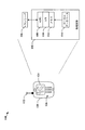
本明細書で開示するいくつかの態様は、電話、モバイルコンピューティングデバイス、ウェアラブルコンピューティングデバイス、アプライアンス、自動車用電子機器、アビオニクスシステムなど、装置の下位構成要素を含み得る電子デバイス間に配備される通信リンクに適用可能であり得る。図1は、ICデバイス間の通信リンクを採用し得る装置を示す。一例では、装置100は、無線周波数(RF)トランシーバを通じて、無線アクセスネットワーク(RAN)、コアアクセスネットワーク、インターネットおよび/または別のネットワークと通信するワイヤレス通信デバイスを含み得る。装置100は、処理回路102に動作可能に結合された通信トランシーバ106を含み得る。処理回路102は、特定用途向けIC(ASIC)108などの1つまたは複数のICデバイスを含み得る。ASIC108は、1つまたは複数の処理デバイス、論理回路などを含み得る。処理回路102は、処理回路102によって実行され得る命令およびデータを維持し得るメモリデバイス112などのプロセッサ可読ストレージを含み得、かつ/またはそれに結合され得る。処理回路102は、オペレーティングシステムによって、および/または、ワイヤレスデバイスのメモリデバイス112などの記憶媒体内に存在するソフトウェアモジュールの実行をサポートし可能にするアプリケーションプログラミングインターフェース(API)110レイヤを通して、制御され得る。メモリデバイス112は、読取り専用メモリ(ROM)もしくはランダムアクセスメモリ(RAM)、電気消去可能プログラマブルROM(EEPROM)、フラッシュカード、または処理システム内およびコンピューティングプラットフォーム内で使用され得る任意のメモリデバイスを含み得る。処理回路102は、装置100を構成かつ操作するために使用される操作パラメータおよび他の情報を維持し得るローカルデータベース114を含み得るか、またはそれにアクセスし得る。ローカルデータベース114は、データベースモジュール、フラッシュメモリ、磁気媒体、EEPROM、光媒体、テープ、ソフトディスクまたはハードディスクなどのうちの1つまたは複数を使用して実装され得る。処理回路はまた、他の構成要素の中でも、アンテナ122、ディスプレイ124などの外部デバイス、ボタン128、キーパッド126などのオペレータ制御に動作可能に結合され得る。
Examples of Devices Employing a Serial Bus Some aspects disclosed herein include device sub-components such as phones, mobile computing devices, wearable computing devices, appliances, automotive electronics, avionics systems, and the like. It may be applicable to communication links deployed between the resulting electronic devices. FIG. 1 shows an apparatus that can employ a communication link between IC devices. In one example,
図2は、通信バスに接続された装置200のいくつかの態様を示すブロック概略図であり、この場合、装置は、ワイヤレスモバイルデバイス、モバイル電話、モバイルコンピューティングシステム、ワイヤレス電話、ノートブックコンピュータ、タブレットコンピューティングデバイス、メディアプレーヤ、ゲーミングデバイス、携帯情報端末(PDA)または他のハンドヘルドデバイス、ネットブック、ノートブックコンピュータ、テレビジョン、エンターテインメントデバイス、ウェアラブルデバイスなどのうちの1つまたは複数において実施され得る。装置200は、シリアルバス230を使用して通信する複数のデバイス202、220、および222a〜222nを含み得る。シリアルバス230は、シリアルバス230によってサポートされる強化された機能のために構成されているデバイスのために、従来のI2Cバスの能力を拡張することができる。たとえば、シリアルバス230は、I2Cバスよりも高いビットレートをサポートすることができる。
FIG. 2 is a block schematic diagram illustrating some aspects of an
図2に示す例では、デバイス202は、シリアルバス230上でスレーブとして動作するように構成され得る。デバイス202は、1つまたは複数の汎用センサー、高速センサー、指紋センサー、画像センサー(たとえば、カメラ)、タッチスクリーンセンサーなどを含む、かつ/または管理する、センサー機能204を提供するように適応され得る。加えて、デバイス202は、構成レジスタまたは他のストレージ206と、制御論理212と、トランシーバ210と、ラインドライバ/受信機214aおよび214bとを含み得る。制御論理212は、状態機械、シーケンサ、信号プロセッサまたは汎用プロセッサなどの処理回路を含み得る。トランシーバ210は、受信機210aと、送信機210cと、タイミング、論理、およびストレージの回路および/またはデバイスを含む共通回路210bとを含み得る。一例では、送信機210cは、クロック生成回路208によって与えられたタイミングに基づいて、データを符号化および送信する。
In the example shown in FIG. 2,
図3は、本明細書で開示するいくつかの態様に従って構成された送信機300および受信機320の一例を示すブロック図である。SGbusの動作の場合、送信機300は、入力データ310を3進(ベース3)数にトランスコードすることができ、3進数は、SCL216およびSDA218信号線上で送信されるべきシンボルにおいて符号化される。図示の例では、入力データ310の各(データワードとも呼ばれる)データ要素は、8、12、16、19、または20ビットなど、事前定義されたビット数を有し得る。トランスコーダ302は、入力データ310を受信し、データ要素ごとに単一の桁の3進数312のシーケンスを生成し得る。場合によっては、単一の桁の3進数312のシーケンスは、複数の桁の3進数として表現され得る。単一の桁の3進数は、2ビットにおいて符号化され得、単一の桁の3進数312の各シーケンス内に12桁あり得る。3進-シンボル変換器304などのエンコーダは、ラインドライバ306のペアに与えられる2ビットシンボル314のストリームを生成する。図示の例では、ラインドライバ306は、SCL216およびSDA218信号線を駆動するオープンドレイン出力トランジスタ308を含む。いくつかの例では、ラインドライバ306は、SCL216およびSDA218信号線を駆動するプッシュプルドライバを含むか、またはそれに結合され得る。3進-シンボル変換器304によって生成された2ビットシンボル314の出力ストリームは、連続するシンボル314の各ペア間のSCL216およびSDA218信号線のうちの少なくとも1つのシグナリング状態における遷移を引き起こす。これらの遷移は、連続するシンボルのペアが2つの同一のシンボルを含まないことを保証することによって与えられる。少なくとも1つのライン216および/または218におけるシグナリング状態における遷移の可用性により、受信機320がデータシンボル314のストリームから受信クロック338を抽出することが可能になる。
FIG. 3 is a block diagram illustrating an example of a
SGbusインターフェースでは、受信機320は、クロックおよびデータ回復(CDR)回路328を含むか、またはそれと協働し得る。受信機320は、CDR回路328に未加工の2ビットシンボル336のストリームを与えるラインインターフェース回路326を含み得る。CDR回路328は、未加工のシンボル336から受信クロック338を抽出し、2ビットシンボル334のストリームおよび受信クロック338を、受信機320の他の回路324および322に与える。いくつかの例では、CDR回路328は、複数のクロックを生成することができる。シンボル-3進変換器324などのデコーダは、受信クロック338を使用して、シンボル334のストリームを12個の3進数332のシーケンスに復号することができる。3進数332は、2ビットを使用して符号化され得る。次いで、トランスコーダ322は、12個の3進数332の各シーケンスを8、12、16、19、または20ビットの出力データ要素330に変換することができる。
In the SGbus interface,
埋込みクロックを用いる遷移符号化方式の例
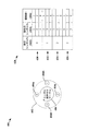
図4は、シリアルバス230上の送信のための埋込みクロックをもつシンボル314のシーケンスを生成するために、3進-シンボル変換器304によって使用され得る符号化方式400を示す図である。符号化方式400はまた、シリアルバス230から受信されたシンボルから3進遷移数を抽出するために、受信機320のシンボル-3進変換器324によっても使用され得る。SGbus符号化方式400では、シリアルバス230の2本のラインにより、4つの基本シンボルS:{0,1,2,3}の定義が可能になる。シンボル314、334のシーケンス内の任意の2つの連続するシンボルは、シリアルバス230上で異なるシグナリング状態を生成し、シンボルシーケンス0,0、1,1、2,2、および3,3は、連続するシンボルの無効な組合せである。したがって、各シンボル境界で3つのみの有効なシンボル遷移が利用可能であり、ここで、シンボル境界は送信クロックによって決定され、第1のシンボル(前のシンボルPs)422が終了し、第2のシンボル(現在のシンボルCs)424が開始するポイントを表す。
Example of Transition Coding Scheme with Embedded Clock FIG. 4 illustrates an encoding that may be used by ternary-to-
本明細書で開示するいくつかの態様によれば、3つの利用可能な遷移には、Psシンボル422ごとに遷移数(T)426が割り当てられる。T426の値は、3進数によって表され得る。一例では、遷移数426の値は、符号化方式用のシンボル順序付けサークル402を割り当てることによって決定される。シンボル順序付けサークル402は、4つの可能なシンボル用のサークル402上のロケーション404a〜404d、およびロケーション404a〜404dの間の回転の方向406を割り振る。図示の例では、回転の方向406は時計回りである。遷移数426は、有効な現在のシンボル424と直前のシンボル422との間の分離を表し得る。分離は、前のシンボル422から現在のシンボルCs424に到達するために必要なシンボル順序付けサークル402上の回転の方向406に沿ったステップの数として定義され得る。ステップの数は、単一の桁のベース3数として表現され得る。シンボル間の3ステップの差分は、0base-3として表され得ることが諒解されよう。図4のテーブル420は、この手法を採用する符号化方式をまとめたものである。
According to some aspects disclosed herein, three available transitions are assigned a transition number (T) 426 for each
送信機300において、前に生成されたシンボル422、および遷移数426として使用される入力3進数を知ると、テーブル420は、送信されるべき現在のシンボル424をルックアップするために使用され得る。受信機320において、テーブル420は、前に受信されたシンボル422と現在受信されたシンボル424との間の遷移を表す遷移数426を決定するためのルックアップとして使用され得る。遷移数426は、3進数として出力され得る。
At the
シリアルバス上の共存
複数のSGbusデバイスは、1つまたは複数のレガシーI2Cデバイスとともに同じバス230上で共存し得る。したがって、SGbusインターフェースは、レガシーI2Cデバイスによって無視されるか、検出されないか、またはさもなければ軽視され得る、シグナリング方式を定義する。たとえば、SGbusデバイスは、I2Cモードシグナリングと一致するシグナリングにおいて制御情報を送信することができ、より高速の送信速度を得るために、CCIeプロトコルに従って符号化されたデータペイロードを送信することができる。SGbusデバイスは、レガシーI2Cモードを含む、データペイロードを送信するための他の符号化モードを使用し得る。代替符号化モードは、シンボルのシーケンス内の連続するシンボル間の遷移において埋め込まれたクロック情報をもつシンボルのシーケンス内でデータを符号化するために、遷移符号化を採用し得る。すなわち、データが3進数にトランスコードされ得、その場合、3進数の各桁は、バスの前のシグナリング状態(すなわち、前のシンボル)に基づいて、次のシンボルを選択する。
Coexistence on Serial Bus Multiple SGbus devices may coexist on the
本明細書で開示するいくつかの態様は、異なる通信プロトコルおよび/またはシグナリングを使用して通信するデバイスのシリアルバス上の共存に関する。いくつかの例では、第1のプロトコルを使用して、シリアルバスを介して通信するように構成されたデバイスは、第2のプロトコルが、第1のプロトコルによって認識されるイベントを生成するシグナリングを採用するとき、第2のプロトコルを使用する他のデバイス間の通信を無視し得る。次に、第1のプロトコルがI2C対応または互換プロトコルであり、第2のプロトコルがCCIe、SGbus、または他のプロトコルである例を使用して、いくつかの態様について説明する。 Some aspects disclosed herein relate to the coexistence of devices communicating using different communication protocols and / or signaling on a serial bus. In some examples, a device configured to communicate over a serial bus using a first protocol may require a second protocol to generate signaling that generates an event recognized by the first protocol. When employed, communication between other devices using the second protocol may be ignored. Some aspects will now be described using an example where the first protocol is an I2C compatible or compatible protocol and the second protocol is CCIe, SGbus, or another protocol.
図5は、I2Cの1バイトデータ書込み動作を示すタイミング図500である。マスタノードが、SCL216が高のままである間にSDA218を低に駆動することによって、START条件506を与えるとき、送信が開始される。I2Cマスタノードは、I2Cバス上のどのスレーブノードにマスタノードがアクセスすることを望むかを示すために、SDA218上で7ビットのスレーブID502と、続いて、動作が読取り動作であるか、書込み動作であるかを示す、読取り/書込みビット512とを送り、それによって、読取り/書込みビット512は、書込み動作を示すために論理0にあり、読取り動作を示すために論理1にある。IDが7ビットのスレーブID502と一致するスレーブノードのみが、書込み(または他の)動作に応答することができる。I2Cスレーブノードがそれ自体のスレーブID502を検出するために、マスタノードは、SCL216上の8個のクロックパルスとともに、SDA218上で少なくとも8ビットを送信する。マスタノードは、SCL216が高のままである間にSDA218を高に駆動することによって、トランザクションを終了させるために、STOP条件516を与える。I2Cインターフェースは、START条件506後に「Bus-Busy」状態であり、STOP条件516後に「Bus-Free」状態であると見なされる。この挙動は、レガシーI2Cスレーブノードが、CCIeプロトコルを含むいくつかのプロトコルによる送信に反応することを防止するために、活用され得る。
FIG. 5 is a timing diagram 500 illustrating an I2C 1-byte data write operation. Transmission begins when the master node provides a
CCIe通信は、データ送信のためにI2CバスのSCL216およびSDA218の組合せを使用し得る。CCIeシンボルは、I2C送信用のSCL216上で送信されたクロック信号パルス514の各トグルに対応する時間において送信され得る。したがって、各フレーム送信期間内に送信されたクロックトグルの数は、CCIe送信ごとに送信され得るシンボルの数を定義し得る。したがって、12シンボル送信は、6-SCLパルスシーケンス中に利用可能な12個のシグナリング状態において与えられ得る。
CCIe communication may use a combination of
I2CバスのSCL216および/またはSDA218は、クロック信号がシンボル遷移内に埋め込まれたとき、CCIeモードにおけるデータ送信のために利用され得る。したがって、SDA218およびSCL216は、レガシーI2Cスレーブノードの機能に影響を与えずに、かつブリッジデバイスを使用してCCIe対応ノードからレガシーI2Cスレーブノードを隔離せずに、任意の12個のシンボルを送信するために使用され得る。I2Cモードでは、START条件506は、I2Cマスタによってのみ与えられ得る。CCIeモードでは、START条件506は、12シンボルワードを送信することになるどのノードによっても与えられる。
The
本明細書で開示するいくつかの態様によれば、SCL216のいくつかのシグナリング特性が活用されるとき、I2Cデバイスは、異なる通信プロトコルを採用するデバイスとともにシリアルバス上で共存し得る。たとえば、スパイク、および/または、50ns以下の持続期間をもつパルスが、I2C高速モード(Fm)またはFm+デバイスと互換性のある、またはそれに対応するデバイスによってフィルタ処理されるというI2C仕様。したがって、I2Cデバイスとともに共有されるシリアルバス上で使用されるプロトコルは、SCL216上のパルスが50ns未満の持続期間に制限される動作モードを含み得る。パルスの持続期間の制限は、SCL216上のハイの状態のクロックパルス生成を制御すること、SCL216のためのゼロ復帰シグナリング方式を実施することによって、および/または、SCL216が50nsの間にハイの状態のままであることを防止するエキストラシンボルを挿入することによって実施され得る。エキストラシンボルは、本明細書ではダミーシンボルと呼ぶことがある。一例では、いくつかのシンボルが50ns期間内に送信され得、エンコーダが、シンボルのシーケンスがSCL216を50nsの間にハイの状態に維持する可能性が高いことを検出するとき、エンコーダは、50ns高期間が完了する前に、SCL216を低になるように強制するダミーシンボルを挿入し得る。
According to certain aspects disclosed herein, when some signaling characteristics of
ダミーシンボルの挿入は、余分なパルス(ダミーパルス)がシリアルバスの1つまたは複数の信号線上で送信されることを引き起こし得る。上記で説明したI2Cの例では、ダミーシンボルは、2つの連続するシンボルがSCL216を論理がハイの状態に維持することになるとき、SCL216上で論理がローの状態に強制的にするために挿入され得る。ダミーシンボルの送信後、SCL216は、2つの連続するシンボルにおける第2のシンボルに対応する論理がハイの状態に戻る。場合によっては、ゼロ復帰(RZ)シグナリングが、SCL216上で長い持続期間の正パルスを防止するために、SCL216上で使用され得る。場合によっては、ハードウェア論理は、SCL216が事前定義された時間期間の間にハイの状態のままであるとき、短い持続期間の論理がローのパルスを挿入することによって、SCL216をポリシングするように構成され得る。
Insertion of a dummy symbol can cause extra pulses (dummy pulses) to be transmitted on one or more signal lines of the serial bus. In the I2C example described above, a dummy symbol is inserted to force the logic on SCL216 to a low state when two consecutive symbols will keep the SCL216 in a high state. Can be done. After transmitting the dummy symbol, the
ダミーパルスは、遷移シンボル符号化が使用されるとき、見掛けのクロックパルスの持続期間を制限する以外の目的で、シリアルバスの1つまたは複数の信号線上に挿入され得る。ダミーパルスは、同期イベントまたは条件を示し得る、求められていない状態の発生を回避するために与えられ得る。たとえば、I2C STARTおよびSTOP条件は、SDA218が変化しないままである間にSCL216が低になるときに示され得、ダミーパルスは、シリアルバスがI2C以外のプロトコルによる通信のために使用されるとき、そのような指示を防止するために、SDA218上に挿入され得る。
Dummy pulses may be inserted on one or more signal lines of the serial bus for purposes other than limiting the duration of the apparent clock pulse when transition symbol encoding is used. Dummy pulses may be provided to avoid the occurrence of an undesired condition that may indicate a synchronization event or condition. For example, I2C START and STOP conditions may be indicated when
通信プロトコル間の遷移
図6は、共有バス602がI2Cデバイス6041〜604k、606、ならびにSGbusデバイス612、6141〜614nおよび6161〜616mを結合する構成を示す。SGbusデバイス612、6141〜614nおよび6161〜616mは、従来のように構成されたI2Cデバイス6041〜604k、606と共存することができ、SGbusデバイス612、6141〜614nおよび6161〜616mのうちのいくつかは、要望または必要に応じて、従来のI2Cプロトコルを使用して通信することができる。
Transition diagram 6 between the communication protocol, showing the configuration of shared
構成および他のバス制御メッセージを含む、共有バス602上のデータ転送は、I2Cプロトコルの変更バージョンまたはI2Cプロトコルの変形態など、第1のプロトコルを使用して開始かつ実行され得る。一例では、すべてのトランザクションは、そのトランザクションを開始するために従来のI2Cプロトコルを使用して開始され得る。
Data transfer on the shared
本明細書で開示するいくつかの態様によれば、共有バス602に結合されたデバイス間のデータ転送が、バス管理および/または制御コマンド間で発生するトランザクション(コンテナ)においてカプセル化されるように、共有バス602上の通信が有効にコンテナ化され得る。典型的には、現在のトランザクションに従事しているデバイスによって採用されたプロトコルを使用して通信するように構成されるデバイスは、そのトランザクションを無視するか、またはそれに気づかないことがある。
According to some aspects disclosed herein, data transfer between devices coupled to a shared
図7は、共有バス602のコンテナまたは動作モード間で遷移するための一般化された方式を示す流れ図700である。各コンテナ、動作モード、および/またはプロトコルは、共有バス602の対応する動作状態702、704、706、708、710に関連付けられ得る。バスの動作モードは、シグナリング方式、データスループット、送信フォーマットなどの間で区別することができる。異なる動作モードが、プロトコルに対して定義され得る。たとえば、12シンボルモードおよび20シンボルモードが、CCIeプロトコルに対して定義され得る。
FIG. 7 is a
動作時、共通プロトコル状態704は、すべてのバスマスタデバイスによって、および/またはバス上のすべてのデバイスによって理解される共通プロトコルを使用して、バス管理コマンドを交換するために使用される。一例では、単一プロトコルスレーブデバイスは、共通プロトコルを使用して通信することができないことがあり、したがって、バス管理コマンドを無視することがある。この後者の例では、バスマスタデバイスは、共有バス602を制御し、単一プロトコルスレーブデバイスによって理解されるプロトコルを使用して、単一プロトコルスレーブデバイスと通信し得る。
In operation, the
いくつかの例では、I2Cプロトコルが共通プロトコル状態704において使用される。他の例では、異なるプロトコルが共通プロトコル状態704において使用され得る。共有バス602は、スタートアップ状態702に初期化され得、それによって、共有バス602に結合されたデバイスが、共通プロトコルのために構成される。共通プロトコルの単一バスマスタの実装形態では、指定されたバスマスタは、共通プロトコルによって定義されたプロシージャに従って、共有バス602に結合された他のデバイスを発見かつ/または構成し得る。マルチマスタ実装形態では、1つまたは複数のマスタデバイスが、発見、構成、および/またはアービトレーションプロセスに参加して、共通プロトコル状態704に入るときに、どのバスマスタが共有バス602を制御するかを決定し得る。バス階層の概念が採用されることがあり、その場合、1つのバスマスタデバイスが、任意の時間に共有バス602のアクティブな制御を有し、他のバスマスタデバイスが、共有バス602のグラント制御を要求し、待機する。
In some examples, the I2C protocol is used in
共通プロトコル状態704では、1つまたは複数のデバイスが、共有バス602の制御を求めて競合し得る。共有バス602は、共有バス602に結合されたデバイス間の通信トランザクションを可能にするために、所望のまたはアービトレートされたプロトコル状態706、708において操作され得る。トランザクションの完了時に、共有バス602は共通プロトコル状態704に戻される。共有バス602へのアクセスを要求中であるデバイスがないとき、共有バス602はアイドル状態710に入り得る。アイドル状態では、1つまたは複数のデバイスが電源切断動作モードに入り得る。バスマスタデバイスは、いずれかのデバイスが共有バス602へのアクセスを要求中であるか否かを決定するために、共有バス602が共通プロトコル状態704に定期的に入ることを引き起こし得る。場合によっては、共有バス602は、割込みまたは他のイベントに応答して、共通プロトコル状態704に戻され得る。
In the
プロトコル状態704、706、708に入ること、およびプロトコル状態704、706、708から出ることは、バス管理コマンドを使用して実施され得る。これらのコマンドは、シグナリング、メッセージング、または、共有バス602のアーキテクチャおよび設計に基づいて選択されたシグナリングおよびメッセージングの何らかの組合せを使用して実施され得る。
Entering and exiting protocol states 704, 706, 708 may be implemented using bus management commands. These commands may be implemented using signaling, messaging, or some combination of signaling and messaging selected based on the architecture and design of shared
データ転送は、共通プロトコル状態704、または、共有バス602に結合されたデバイスのサブセットによって使用されるプロトコル状態706、708のうちの1つにおいて発生し得る。デバイスのサブセットによって使用されるプロトコル状態706、708は、共有バス602と互換性のある任意のプロトコルであり得る。データは、ワード、フレーム、および/またはパケット単位で転送され得、柔軟なデータ転送モードが企図される。
The data transfer may occur in a
場合によっては、アドレスが、共有バス602に結合されたデバイスに動的に割り振られ得る。一例では、共通プロトコルを使用して通信するデバイスの一意の識別情報を提供するために、およびそのようなデバイスのための優先度ランク付けを割り当てるために、動的アドレス割振りが共通プロトコル状態704において実行される。場合によっては、共通プロトコル以外のプロトコルを使用して通信するデバイスの一意の識別情報を提供するために、およびそのようなデバイスのための優先度ランク付けを割り当てるために、動的アドレス割振りが、他のプロトコル状態706、708のうちの1つまたは複数において実行される。
In some cases, addresses may be dynamically allocated to devices coupled to shared
場合によっては、例外処理方式が共通プロトコル状態704のために定義される。たとえば、I2C互換帯域内割込みプロシージャは、共通プロトコルがI2CまたはI2Cの派生物であるときに提供され得る。
In some cases, an exception handling scheme is defined for
場合によっては、「ホットプラグ」プロシージャが実施されることがあり、その場合、そのホットプラグプロシージャは、帯域内割込みプロシージャおよび動的アドレス割振りプロシージャを含み、かつ/または使用する。 In some cases, a "hot-plug" procedure may be implemented, where the hot-plug procedure includes and / or uses an in-band interrupt procedure and a dynamic address allocation procedure.
図8は、本明細書で説明するいくつかの態様による、共有バス602がそれぞれビットおよびシンボル802送信済みI2CおよびSGbusプロトコルを伴う通信トランザクションをサポートする一例のための、共有バス602上で実行されるトランザクション800を示す。最初に、共有バス602は、Bus-Free状態822であり得、制御シグナリング806は、一般に理解されるI2Cプロトコルに従って扱われる。制御シグナリング806が、824、826で肯定応答された後、SGbusデータ交換808が発生し得、その間に、データペイロード810がSGbusマスタデバイス612に送信される。終了シーケンス812は、SGbusデータ交換808(すなわち、SGbusプロトコルによるシグナリング)から、I2Cプロトコルと一致するSTOP条件820、516として認識されるシグナリングへの遷移を与える。次いで、Bus-Free状態822(図7のアイドル状態710も参照)が生じ得る。
FIG. 8 is implemented on shared
図示の例では、共有バス602上のトランザクション800が、アドレス816(たとえば、I2CスレーブID502を参照)と後に続くコマンドコード818の連続とに先行するI2C START条件814(図5のSTART条件506も参照)によって開始され得る。コマンドコード818は、共有バス602のために使用されるSGbus通信プロトコルによって事前定義されたバイト数を含み得る、可変長を有し得る。
In the example shown, the
一例では、コマンドコード818は、選択されたデータ転送プロトコル、および/またはデータ転送プロトコルのいくつかの特性を定義するために送信され得る。この後者のコマンドコードは、後続のデータ転送のために使用されるべき複数の利用可能なデータ転送プロトコルのうちの1つを識別し得る。識別されたデータ転送プロトコルは、異なるデータ転送プロトコルコマンドがバス上に挿入されるまで、トランザクションを制御し得る。
In one example,
START条件814の後、次のSTOP条件820(図5のSTOP条件516も参照)まで、共有バス602はビジーであると見なされる。Bus-Free状態822は、SCL216およびSDA218が所定の時間期間の間に論理がハイの状態であるとき、発生中であると定義され得る。共有バス602のビジー/フリー状態は、START条件814、506、およびSTOP条件820、516の発生に基づいて、定義または識別され得る。Bus-Free状態822は、STOP条件820、516の後の時間期間を含む持続期間を有し、その間に、データがSGbusプロトコルを使用して転送されるか、I2C互換プロトコルを使用して転送されるかにかかわらず、SCL216およびSDA218が論理がハイの状態である。一例では、その間にSCL216およびSDA218が論理がハイの状態である時間期間が、共有バス602上で使用される最も遅いクロックの周期の2倍になるように設定され得る。たとえば、I2C高速モードでは、SCL216上で送信されるクロック信号は、2.5μsのクロック周期とともに、少なくとも400kHzの周波数を有し、5μs周期が、Bus-Free状態822を示すために十分であり得る。
After
図6に示すように、共有バス602は、レガシーI2Cマスタデバイス606と、レガシーI2Cスレーブデバイス6041〜604kと、プライマリSGbusマスタデバイス612と、SGbusスレーブデバイス6141〜614nと、SGbusセカンダリマスタデバイス6161〜616mとをサポートし得る。プライマリSGbusマスタデバイス612は、典型的には、共有バス602上に存在するレガシーI2Cデバイス606、6041〜604kに関係するある動作情報を用いて事前構成される。プライマリSGbusマスタデバイス612は、それにおいて動作情報および他の情報が、アプリケーションホストデバイスから受信された通信に応答して事前構成かつ/または更新され得る、不揮発性メモリを含み得る。
As shown in FIG. 6, the shared
セカンダリSGbusマスタデバイス6161〜616m、およびSGbusスレーブデバイス6141〜614nの各々は、任意の所望の、構成された、または事前定義された長さのランダムアドレスを内部で生成するように構成され得る。一例では、ランダムアドレスは48ビットを有し得る。これらのデバイス6141〜614n、6161〜616mは、ローカルアドレスが割り当てられていないデバイスの存在を識別するために使用され得る予約済みアドレスを使用して、割込みを引き起こすことが可能であり得る。 Each of the secondary SGbus master devices 616 1 to 616 m and the SGbus slave devices 614 1 to 614 n are configured to internally generate a random address of any desired, configured, or predefined length. Can be done. In one example, the random address may have 48 bits. These devices 614 1 ~614 n, 616 1 ~616 m is capable of using the reserved address that can be used to identify the presence of a device not assigned a local address causes an interrupt obtain.
動作時、プライマリSGbusマスタデバイス612は、一般呼出しと、後に続く動的アドレス割振りコマンドコードとを送信し得る。次いで、プライマリSGbusマスタデバイス612は、論理がハイのレベルにプルされ得るSDA218を解放しながら、共有バス602のSCL216上でクロック信号を駆動し得る。アービトレーションプロセスが後に続き、それによって、SGbusデバイス6141〜614n、6161〜616mは、それらの対応するランダムに選択された48ビットアドレスに従って、SDA218を駆動する。SGbusデバイス6141〜614n、6161〜616mのうち最低のアドレスをもつものが、I2Cプロトコルによって規定されるような同様の方式で、アービトレーションを勝ち取る。
In operation, the primary
プライマリSGbusマスタデバイス612は、SCL216上でクロック信号を駆動し続け、SDA218が解放される。次いで、SGbusデバイス6141〜614n、6161〜616mの中から勝ったデバイスは、1つまたは複数の特性バイトを転送し得る。特性バイトは、デバイスがスレーブデバイスのみとして機能するか否か、デバイスのタイプ(たとえば、加速度計)、データ幅(たとえば、16または12ビット幅)、および他の特性を含む、勝ったデバイスのいくつかの特性を識別する情報を含む。
Primary
プライマリSGbusマスタデバイス612は、勝ったデバイスのための7ビット幅ローカルアドレスを転送し得る。このアドレスは、プライマリSGbusマスタデバイス612が識別されたデバイスに割り当てる優先度レベルを組み込む。プライマリSGbusマスタデバイス612は、アドレスアービトレーションを求めるデバイスからの応答を受信しなくなるまで、このプロシージャを繰り返し得る。プライマリSGbusマスタデバイス612は、プロシージャに入ることを可能にした動的アドレス割振りコマンドコードを終了させる特定のコマンドコードを送ることによって、アービトレーションプロシージャを終了させ得る。
Primary
共有バス602に接続されたセカンダリSGbusマスタデバイス6161〜616mは、アービトレーションプロセスを監視し、そのプロセス中に情報交換を取り込むことができ、セカンダリSGbusマスタデバイス6161〜616mは、共有バス602のためのアドレス指定、優先度、および構成情報のコピーを有するようになる。それにもかかわらず、プライマリSGbusマスタデバイス612は、SGbusスレーブデバイス6141〜614nから受信された情報を、セカンダリSGbusマスタデバイス6161〜616mに転送し得る。
The secondary SGbus master devices 616 1 to 616 m connected to the shared
SGbusデバイス6141〜614n、6161〜616mの各々は、動的アドレスを記憶するために使用され得る1つまたは複数の保持レジスタを有することができ、SGbus構成が、コールド電源投入後に使用するために確保され得るようになる。2つのSGbusデバイス6141〜614nおよび/または6161〜616mが、同じランダムな48ビットアドレスを選択し、同じ特性バイトを有する場合、2つのデバイスは同じローカルアドレスを記憶し得る。二重割当ては、実際には、SGbusマスタデバイス612がデータ転送を必要とし、2つの異なるSGbusスレーブデバイス6141〜614nによって同時に送信されたデータが異なるまで、残り得る。2つのSGbusスレーブデバイス6141〜614nのうちの少なくとも1つは、共有バス602に接続された別のSGbusスレーブデバイス6141〜614nと同じアドレスを有することを認識することができ、共有バス602から外れることができる。次のBus-Free状態822において、外されたSGbusスレーブデバイス6141〜614nは、この要件のための専用の制御コードを使用して、新しいローカルアドレスを要求し得る。本明細書で開示するいくつかの態様によって適応され得る既存のプロシージャを含む、同じローカルアドレスの二重割当てを識別するための他のプロシージャが利用可能であり得る。たとえば、プライマリまたはメインマスタデバイスは、ローカルアドレスを必要とするデバイスの数を知らされ得、より少ないローカルアドレスが割り振られるかまたは割り当てられる場合、メインマスタは回復プロシージャを開始かつ/または実行し得る。回復プロシージャの一例では、動的アドレス割当てプロシージャが最初から再開され得る。信頼できるフォールバックプロシージャの他の例は、2つ以上のデバイスが重複アドレスを有する場合からの回復において使用するために利用可能である。
Each of the SGbus devices 614 1 to 614 n , 616 1 to 616 m can have one or more holding registers that can be used to store dynamic addresses, and the SGbus configuration is used after cold power up To be able to be secured. If two SGbus devices 614 1 -614 n and / or 616 1 -616 m select the same random 48-bit address and have the same property byte, the two devices may store the same local address. Double allocation is actually to
SGbusデバイス6141〜614nおよび/または6161〜616mの各々は、プライマリSGbusマスタデバイス612によって優先度ランク付けを割り当てられる。優先度ランクは、SGbusマスタデバイス612によって、動的に割り振られたローカルアドレスのレベルを使用して定義され得、それによって、より低いアドレス値がより高い優先度ランクを有する。
Each of the SGbus devices 614 1 -614 n and / or 616 1 -616 m is assigned a priority ranking by the primary
SGbusデバイス6141〜614n、6161〜616mの各々は、Bus-Free状態中の任意の時間に帯域内割込み要求(IRQ)をアサートすることができる。IRQアサーションプロシージャは、I2Cおよび他のI2C関連インターフェースにおいてバスアービトレーションのために使用される同様のプロシージャに対応する。しかしながら、本明細書で開示するいくつかの態様によれば、いくつかの改良および強化がIRQプロシージャのために採用され得る。 Each SGbus device 614 1 ~614 n, 616 1 ~616 m can assert band interrupt request (IRQ) at any time during the Bus-the Free state. The IRQ assertion procedure corresponds to a similar procedure used for bus arbitration in I2C and other I2C related interfaces. However, according to certain aspects disclosed herein, certain improvements and enhancements may be employed for the IRQ procedure.
一例では、SGbusスレーブデバイス6141〜614nは、SDA218を論理がローのシグナリング状態にプルすることによって、帯域内IRQをアサートすることができる。プライマリSGbusマスタデバイス612は、SDA218を駆動されないままにしながら、SCL216上でクロック信号を駆動することを開始し得る。SDA218は、論理がハイのシグナリング状態の方にプルされ得る。SGbusスレーブデバイス6141〜614nは、それ自体のアドレスを送信するために、SDA218を駆動し得る。プライマリSGbusマスタデバイス612は、IRQを認め、次いで、SGbusスレーブデバイス6141〜614nから受信されたアドレスを使用して、反復STARTを実行する。SCL信号線924がBus-Busy状態中に高である間、およびSTOP条件908が期待されることになるとき、SDA信号線922を低に駆動することによって、反復START条件928(図9参照)が与えられる。デバイス6141〜614n、6161〜616m、および/または6041〜604kは、反復START条件928を検出した後、それらのそれぞれのアドレスについてバスを監視し得る。
In one example, SGbus slave devices 614 1 ~614 n, by the SDA218 logic to pull the signaling state of the row, can assert a band IRQ. Primary
プライマリSGbusマスタデバイス612は、前に定義されたモードが現在所望または必要とされるモードとは異なる場合、データ転送プロトコルバイトを使用して、データ転送モードを随意に構成し得る。次いで、プライマリSGbusマスタデバイス612および割り込むSGbusスレーブデバイス6141〜614nは、通信を開始し得る。バス競合はアドレス評価中に行われ、同時にバスを勝ち取ろうと試みている任意の追加のSGbusデバイス6141〜614n、6161〜616m、および/または任意のレガシーI2Cデバイス6041〜604kは、そのアービトレーションに負けることになり、次のBus-Free状態822において再試行し得る。
The primary
別の例では、セカンダリSGbusマスタデバイス6161〜616mは、SGbusスレーブデバイス6141〜614nのためのものと同様であるプロシージャを使用して、帯域内IRQをアサートすることができる。プライマリSGbusマスタデバイス612が、IRQがセカンダリSGbusマスタデバイス6161〜616mによってアサートされることを認識するとき、プライマリSGbusマスタデバイス612は、SCL216を解放し、セカンダリSGbusマスタデバイス6161〜616mは、通信のためのターゲットデバイスをアドレス指定するために、即時反復START条件928を実行する。
In another example, secondary SGbus master devices 616 1 -616 m may assert an in-band IRQ using a procedure similar to that for SGbus slave devices 614 1 -614 n . When the primary
別の例では、レガシーI2Cマスタデバイス606は、セカンダリSGbusマスタデバイス6161〜616mについて説明したものと同様であるプロシージャにおいて、IRQをアサートし得る。レガシーI2Cマスタデバイス606は、典型的には、いつそれがSGbusマスタデバイス612と競合中であるかに気づいておらず、その理由は、SGbusマスタデバイス612が等価のより高いアドレス(たとえば、111 1111)を有し、アービトレーションに負けることになるからである。いくつかの適用例では、I2Cデバイスなどのより遅いレガシーデバイスをSGbusから除外することが望ましくなり得ることは諒解されよう。たとえば、レガシーデバイスは、バス速度(スループット要件)のために、または、共存を可能にするために必要とされるプロシージャの複雑さのために、排除され得る。
In another example, legacy
通信トランザクションを開始するプライマリSGbusマスタデバイス612は、アドレス呼出し中に、アドレスアービトレーションプロシージャを評価する。任意のSGbusスレーブデバイス6141〜614n、セカンダリSGbusマスタデバイス6161〜616m、または、プライマリSGbusマスタデバイス612に割り込むことを試みるレガシーI2Cマスタデバイス606は、典型的に成功する。しかしながら、より低い優先度ランクを有するいかなるデバイスも、次のBus-Free状態822を待機しなければならないことがある。
The primary
場合によっては、レガシーI2Cマスタデバイス606とSGbusスレーブデバイス6141〜614nとの間で競合があり得る。プライマリSGbusマスタデバイス612は、START条件を見るとき(すなわち、SDA218が低になるとき)、SCL216上でクロック信号を開始する。したがって、より高い優先度ランクを有するSGbusスレーブデバイス6141〜614nは、仮定によるとアービトレーションプロセスを勝ち取る。プライマリSGbusマスタデバイス612は、勝ったアドレスを含む、アービトレーションプロセスの結果を承知している。
In some cases, there may be a competition between the legacy
本明細書で開示するいくつかの態様によれば、SGbusは、1つまたは複数のSGbusマスタデバイス612、6161〜616m、およびレガシーI2Cマスタデバイス606が、対応するスレーブデバイスのためのバス制御および管理機能を提供する、マルチマスタバスであり得る。SGbusにおいて採用されるいくつかのマルチマスタアービトレーションおよびバス制御プロシージャは、IRQプロシージャについて説明されるものなど、グローバルなルールに従い得る。したがって、I2Cルールは、レガシーI2Cマスタデバイス606が1つまたは複数のSGbusセカンダリマスタデバイス6161〜616mと競合するとき、適用され得る。
According to some aspects disclosed herein, SGbus is one or more SGbus master device 612,616 1 ~616 m and legacy
SGbusセカンダリマスタデバイス6161〜616mが、トランザクションを実行するために共有バス602の制御を獲得するとき、SGbusセカンダリマスタデバイス6161〜616mは、トランザクションを実行することが必要とされる限りの間のみ、共有バス602の制御を維持する。それぞれのトランザクション後、STOP条件820は、バス制御をプライマリSGbusマスタデバイス612に復帰させる。
When the SGbus secondary master devices 616 1 to 616 m gain control of the shared
レガシーI2Cマスタ606は、一般にデータをレガシーI2Cスレーブデバイス6041〜604kへ転送し、CCIeデータ転送プロトコルなどの他のデータ転送プロトコルが利用可能であるときでも、I2C対応プロトコルを採用する。レガシーI2Cマスタ606とSGbusデバイス6141〜614n、6161〜616mとの間の通信は、システムレベルで管理され得る。一例では、プライマリSGbusマスタデバイス612は、レガシーI2Cマスタ606にSGbusスレーブデバイス6141〜614nの存在を知らせ得る。プライマリSGbusマスタデバイス612は、SGbusスレーブデバイス6141〜614nのローカルアドレスおよび特性に関する情報を提供し得る。レガシーI2Cマスタ606とSGbusスレーブデバイス6141〜614nとの間で得られたいかなる通信も、I2Cプロトコルと一致し得る。
本明細書で開示するいくつかの態様によれば、SGbusは、SGbusデバイス612、6141〜614n、または6161〜616mが、すでに動的に構成されておりオプションであるバス602に挿入され得る、ホットプラグ能力をサポートし得る。ホットプラグされたSGbusデバイス612、6141〜614n、または6161〜616mは、バス上で電源投入し、コールド電源投入と同様の条件を仮定し、ホットプラグされたSGbusデバイス612、6141〜614n、または6161〜616mは、割り当てられたローカルアドレスを最初は有していない。割り当てられたローカルアドレスを有していないデバイス612、6141〜614n、または6161〜616mは、ローカルアドレスを必要とするというインジケータとして事前定義されたバイトを使用して、IRQを実行し得る。IRQ、および、ホットプラグされたSGbusデバイス612、6141〜614n、または6161〜616mの共有バス602上の存在を検出すると、プライマリSGbusマスタデバイス612は、本明細書で説明するような、動的アドレス割振りプロシージャを実行し得る。
According to some aspects disclosed herein, the SGbus inserts an
本明細書で開示するいくつかの態様によれば、SGbusは、I2Cプロトコル、CCIプロトコル、およびそれらの変形態、ならびに他のプロトコルを含む、複数のデータ転送プロトコルをサポートし得る。一例では、CCI拡張(CCIe)バスが、SGbus上でデータトランスポートを提供するために使用され得る。CCIe通信およびI2C通信は、共有バス602上で実行され得るので、第1の時間間隔において、データがCCIe符号化を使用して送信され得、他のデータがI2Cのシグナリング規約に従って異なる時間間隔において送信され得るようになる。SGbusは、CCIe送信がI2Cプロトコルに違反しないことを保証する物理レイヤプロトコルを採用する。
According to some aspects disclosed herein, SGbus may support multiple data transfer protocols, including I2C protocol, CCI protocol, and variants thereof, as well as other protocols. In one example, a CCI extension (CCIe) bus may be used to provide data transport over SGbus. Since CCIe and I2C communications may be performed on shared
図9は、I2Cバス上の複数のデータ送信に関連付けられたタイミングを示すタイミング図900および920を含む。第1の基本的な例では、STOP条件908と連続するSTART条件910との間に経過する時間期間(アイドル期間914)が長い場合があり、それによって、従来のI2Cバスはこのアイドル期間914の間にアイドルになる。動作時には、I2Cバスマスタが第1のSTART条件906と後に続くデータとを送信するとき、ビジー期間912が開始する。ビジー期間912は、I2CバスマスタがSTOP条件908を送信するときに終了し、アイドル期間914が後に続く。アイドル期間914は、第2のSTART条件910の送信とともに終了する。
FIG. 9 includes timing diagrams 900 and 920 showing timing associated with multiple data transmissions on the I2C bus. In a first basic example, the time period (idle period 914) that elapses between a
また、タイミング図920を参照すると、場合によっては、I2Cバス上の連続するデータ送信間のアイドル期間914は、STOP条件908ではなく反復START条件(Sr)928を送信することによって、数が減らされるかまたは除去され得る。反復START条件928は、先行するデータ送信を終了させ、同時に次のデータ送信の開始を示す。SDA信号線922上の状態遷移は、アイドル期間930後に生じるSTART条件926と反復START条件928とで同一である。詳細には、SDA信号線922は、SCL信号線924が高である間に、高から低に遷移する。データ送信間に反復START条件928が使用されるとき、第1のビジー期間932の直後に第2のビジー期間934が生じる。
Also referring to the timing diagram 920, in some cases, the idle period 914 between successive data transmissions on the I2C bus is reduced by transmitting a repeated START condition (Sr) 928 instead of a
SGbusでは、データ転送セグメントは、任意のI2C、CCIe、もしくは別の遷移符号化プロトコル、またはそれらの変形態を使用することができる。使用されるべきデータ転送プロトコルのタイプは、SGbusスレーブデバイス6141〜614nとの通信の開始時に、SGbusマスタデバイス612、または6161〜616mによって示され得る。各SGbusスレーブデバイス6141〜614nのためのデータ転送プロトコルの選択は、実際には、SGbusマスタデバイス612、または6161〜616mによって変更されるまで、そのままである。場合によっては、プライマリSGbusマスタデバイス612は、I2Cモードをデフォルトモードとして使用するために、I2CモードとCCIeモードの両方で通信することができる任意のデバイスを構成し得る。
In the SGbus, the data transfer segment may use any I2C, CCIe, or another transition coding protocol, or a variant thereof. Type of data transfer protocol to be used, at the start of communication with the SGbus slave devices 614 1 ~614 n, it may be indicated by
データ転送から出ることは、STOP条件820、908を共有バス602上で挿入することによって実施され得、その場合、共有バス602はBus-Free状態822に入り得る。共有バス602上のトランザクションにおいて送信されたいくつかのシンボルのシーケンスは、トランザクションにおける参加者ではない1つまたは複数のデバイス6041〜604k、6141〜614n、6161〜616mの検出論理によって、STOP条件820、908、または反復START条件928として識別され得るシグナリング状態を生成し得る。
Exiting the data transfer may be implemented by inserting
図10は、通常のデータ交換中に、および/または、同期論理における図示された準安定性の問題のために生じ得る、意図しないSTART条件1008および意図しないSTOP条件1012の発生を示す。意図しないSTOP条件1012および意図しないSTART条件1008は、意図しないSTOP条件1012および意図しないSTART条件1008を引き起こし得るシンボルのシーケンスを識別するようにエンコーダを構成することによって、回避され得る。エンコーダは、意図しないおよび求められていないSTOP条件1012、ならびに/または意図しないSTART条件1008を生成することを回避するために、送信シンボルのストリームを修正し得る。一例では、コーディングプロトコルは、データ転送モードである間に意図しないSTOP条件1012を回避するために、任意の2進「01」シンボルの後、2進「00」ダミーシンボル挿入を与え得る。別の例では、コーディングプロトコルは、誤ったまたは意図しないSTART条件1008の後、レガシーI2Cデバイスにそのアドレスについて検査させ得る、意図しないSTART条件1008を回避するために、2進「11」シンボルのいずれかの発生後に2進「10」ダミーシンボル挿入を与え得る。レガシーI2Cデバイスは、アドレス一致を発見する場合、誤ったまたは意図しないSTART条件1008に応答し、それによって、CCIeアクティブドライバに悪影響を及ぼすことがあることは諒解されよう。
FIG. 10 illustrates the occurrence of an
CCIeモードのデータ転送では、データ転送モードへのエントリポイント後に送られた最初のシンボルで開始する、共有バス602上で送信されたシンボルのカウントに基づいて、フレーム同期が実行され得る。SGbus動作では、反復START条件928がフレーム内の12シンボルの各シーケンスまたは20シンボルの各シーケンスの前に送られる必要はない。反復START条件928の不在によって、データスループットを高めることができる。
For data transfer in CCIe mode, frame synchronization may be performed based on a count of symbols transmitted on shared
場合によっては、フレーム同期は、誤り検出のために使用される最後の3つの最下位ビット(LSB)「000」を検査することによって、さらに検証され得る。単一の誤りは、2進の復号された数の最後の3つのLSBを検査することによって、検出され得る。単一の誤りは、任意の12シンボルワード上のシンボル誤りに関係することがあり、その場合、どの2つの連続するシンボルも等しくない。シンボルは、2進数[SDA:SCL]として符号化され得、その場合、SDA218のシグナリング状態に対応するビットは、最上位ビット(MSB)位置にある。1つのシンボル誤りは、SDA218またはSCL216の一方または両方のサンプリングされたシグナリング状態における誤りの結果であり得る。
In some cases, frame synchronization may be further verified by examining the last three least significant bits (LSB) “000” used for error detection. A single error may be detected by examining the last three LSBs of the binary decoded number. A single error may relate to a symbol error on any 12 symbol words, in which case no two consecutive symbols are equal. The symbol may be encoded as a binary number [SDA: SCL], in which case the bit corresponding to the signaling state of
図11を参照すると、ならびに図3および図4に関して説明したように、送信機300のトランスコーダ302によって生成された3進数は、サークル402上およびその全体にわたる変位値として表され得る。一例では、時計回りの変位は3進値T=1として表され得、反時計回りの変位は3進値T=0として表され得、サークル402の全体にわたる変位(すなわち、2ステップ時計回りまたは反時計回り)は、3進値T=2として表され得る。
Referring to FIG. 11, and as described with respect to FIGS. 3 and 4, the ternary numbers generated by
直接の結果として、サークル402上の隣接するシンボルのいずれかに等しいシンボルを生じるライン誤りは、新しいシンボルとは見なされず、誤りはワードレベルで識別され得る。しかしながら、単一のシンボル誤りは、2つの隣接する3進数が修正される結果となる。
Line errors that directly result in a symbol equal to any of the adjacent symbols on
本明細書で開示するいくつかの態様によれば、誤り訂正がSGbus通信のために提供され得る。データを転送するために、情報の2進列が、ベース3(3進)数としてコーディングされた、等しい数値に変換され得る。したがって、より少ない文字が、同じ情報のためにノード間で送信される必要がある。変換された3進数は多項式の和であり、ただし、因数は3の累乗であり、係数は[0,1,2]である。 According to some aspects disclosed herein, error correction may be provided for SGbus communication. To transfer data, a binary sequence of information may be converted to an equal number coded as a base 3 (ternary) number. Thus, fewer characters need to be transmitted between nodes for the same information. The converted ternary number is a sum of polynomials, where the factor is a power of 3 and the coefficient is [0,1,2].

ただし、Tk=3進係数、∈[0,1,2]である。 Here, T k = a ternary coefficient, ∈ [0,1,2].
1つのシンボル誤りは、2つの隣接するTk値の改変を生じることがあり、最後の和は、次の公式によって改変され得る。
±a×3n±b×3(n-1) (1)
ただし、
「n」=誤ったシンボルのランク、ならびに
「a」および「b」は、差分の係数である。
「a」および「b」係数は、以下を尊重する。
a∈[0,±1,±2]
b∈[0,±1,±2]
One symbol error can cause modification of two adjacent T k values, and the final sum can be modified by the following formula:
± a × 3 n ± b × 3 (n-1) (1)
However,
"N" = rank of the incorrect symbol, and "a" and "b" are the coefficients of the difference.
The “a” and “b” coefficients respect the following:
a∈ [0, ± 1, ± 2]
b∈ [0, ± 1, ± 2]
公式(1)を、次のように書くことができる。
(±3a±b)×3(n-1) (2)
Formula (1) can be written as:
(± 3a ± b) × 3 (n-1) (2)
LSBの最後のビットが誤りによって不変のままで残されるために、公式(2)は、2の累乗の倍数でなければならない。整数倍ではない2の累乗の第1のランクは、1つのシンボル誤りが識別されるものとするように、いくつのLSBエンドビットが事前に知られていなければならないかを示す。因数3(n-1)は、3の倍数であり、改変されない場合、LSBビットを変化させることになる。
Formula (2) must be a power-of-two multiple so that the last bit of the LSB remains unchanged by error. The first rank of a power of two that is not an integer multiple indicates how many LSB end bits must be known in advance so that one symbol error shall be identified.
関連する因数(±3a±b)の解析は、シンボル-3進コーディング図が円対称性を有するという観測に基づき得る。したがって、1点の考察がすべての4点をカバーする。たとえば、「2」が正しいシンボルである場合、いずれかの他の正しいシンボル状況では、それは、それぞれの位置をそれらの回転された値で置き換えるために十分である。以下のTable 1(表1)は、生じる可能性のある「a」係数を示し、Table 2(表2)は、生じる可能性のある「b」係数を示す。 Analysis of the relevant factors (± 3a ± b) may be based on the observation that symbol-ternary coding diagrams have circular symmetry. Therefore, one point of consideration covers all four points. For example, if "2" is the correct symbol, then in any other correct symbol situation, it is enough to replace each position with their rotated value. Table 1 below shows the possible "a" coefficients, and Table 2 shows the possible "b" coefficients.
以下のTable 3(表3)は、生じる可能性のある「a」および「b」係数の組合せを示す。 Table 3 below shows the possible combinations of “a” and “b” coefficients.
可能性のある(a;b)ペアが、同じ可能性のある「誤ったシンボル」に関するものとして、同じ背景行に示されている。直接的な検査によって、それぞれ次のようになる組合せがあることが明らかである。
(±3a±b)=2、たとえば、(1;-1)および(-1;1)、
(±3a±b)=4、たとえば、(-2;2)および(2;-2)である。
(±3a±b)=8をもたらすことになるペアはなく、それは、(2;2)または(-2;-2)のみについて可能であったであろう。
Possible (a; b) pairs are shown in the same background row as relating to the same possible "wrong symbol". It is clear from the direct inspection that there are the following combinations.
(± 3a ± b) = 2, for example, (1; -1) and (-1; 1),
(± 3a ± b) = 4, for example, (-2; 2) and (2; -2).
No pair would result in (± 3a ± b) = 8, which would have been possible only for (2; 2) or (-2; -2).
したがって、LSBエンドにおける任意の既知の3ビットは、任意の1つの単一のシンボル誤りを検出することができる。たとえば、「000」が使用され得るが、任意の他の3つの既知のビットが同じ役割を果たし得る。SDA218またはSCL216におけるいかなる誤りも、最後の3ビットによって検出され得る。
Thus, any known three bits at the LSB end can detect any one single symbol error. For example, "000" may be used, but any other three known bits may play the same role. Any errors in
本明細書で開示するいくつかの態様によれば、補足の誤り検査は、データ転送が進行中である間にSTOP条件908または反復START条件928の誤った識別を回避するために、必要に応じて、シンボル2進「01」から2進「00」への強制的な変換、または、シンボル2進「11」から2進「10」への強制的な変換に基づき得る。複数の12シンボルまたは20シンボルフレームのデータ転送全体の完了時に、STOP条件820、908を生成するために、4つのシンボルが挿入され得、そのうちの最後の2つが、2進「01」と後に続く2進「11」であり得る。
According to some aspects disclosed herein, supplemental error checking may be performed as needed to avoid false identification of a
図12および図13を参照すると、CCIeの前の実装形態と現在説明しているSGbusとの間のいくつかの違いが強調され得る。たとえば、2つのコーディングスタイルは、異なるシンボルを生成し得るが、復号された3進係数は、どちらの場合も同じである。別の例では、SGbusは、共有バス602上の意図しない(および求められていない)STOP条件908および反復START条件928(すなわち、2進「01」から2進「11」への遷移、または2進「11」から2進「10」への変換)を回避する。次いで、いくつかのデータストリームでは、SGbusは、シンボルを送信に追加し、それによってデータスループットを低減する。CCIeインターフェースは、12シンボルフレームごとに送信される境界シーケンスを有するが、SGbusは、フレームごとではなく、データ転送全体の終了において、ただ1つの終了シーケンスを有する。
Referring to FIGS. 12 and 13, some differences between the previous implementation of CCIe and the currently described SGbus may be highlighted. For example, two coding styles may produce different symbols, but the decoded ternary coefficients are the same in both cases. In another example, the SGbus provides an unintentional (and unsolicited)
第1の例では、図12のタイミング図1200は、送信機300のトランスコーダ302によって3進-シンボル変換器304(図3参照)に与えられた、3進送信機(Tx)遷移数1202のシーケンスを示す。変換器は、シリアルバス230を介した受信機320への送信のために、シンボル1204のストリームを生成する。受信機320のシンボル-3進変換器324は、3進受信機(Rx)遷移数1206を生成する。Tx遷移数1202と、シンボル1204と、Rx遷移数1206との数の間に直接的な関係がある。
In a first example, the timing diagram 1200 of FIG. 12 shows the ternary transmitter (Tx)
第2の例では、図12のタイミング図1220は、第1のSGbusデータフレームの送信を示し、それによって、送信機(Tx)3進数1222のシーケンスがトランスコーダ302によって3進-シンボル変換器304(図3参照)に与えられる。ここで、3進-シンボル変換器304は、挿入された追加のシンボル1230を含むシンボル1224のストリームを生成する。受信機320のシンボル-3進変換器324は、3進受信機(Rx)遷移数1226を生成する。シンボル-3進変換器324は、トランスコーダ322によって抽出される追加の数1232を含むRx遷移数1226を生成する。
In a second example, the timing diagram 1220 of FIG. 12 shows the transmission of a first SGbus data frame, whereby a sequence of transmitter (Tx)
図13は、タイミング図1300および1320における第3の例および第4の例を含み、それによって、第3のタイミング図1300は中間および/または最悪状況SGbusフレームに関係し、第4のタイミング図1320は最後のSGbusデータフレームに関係する。これらのタイミング図1300、1320では、3進-シンボル変換器304は、挿入された追加のシンボル1310および1330を含むシンボル1304、1324のストリームを生成する。受信機320のシンボル-3進変換器324は、3進Rx遷移数1306、1326を生成する。シンボル-3進変換器324は、トランスコーダ322によって抽出される追加の3進数1312および1332を含む、Rx遷移数1306、1326を生成する。
FIG. 13 includes third and fourth examples in timing diagrams 1300 and 1320 whereby the third timing diagram 1300 relates to an intermediate and / or worst case SGbus frame and a fourth timing diagram 1320 Refers to the last SGbus data frame. In these timing diagrams 1300, 1320, the ternary-to-
異なるデータ転送モードが、バスクライアントの性質に基づいて使用するために選択されたモードとともに、共有シリアルバス上で使用するために利用可能であり得る。一例では、12シンボルフレームを使用する修正されたCCIeデータ転送モードが、I2Cデバイスがバス上に存在しないか、または参加中ではないときに利用可能であり、このモードではダミー変換の必要はない。別の例では、I2Cデバイスは共有バス602上に存在し、修正されたCCIeデータ転送モードが、12シンボルフレームおよびダミー変換とともに採用される。このデータ転送モードの特性は、I2Cクライアントの能力に依存し得る。
Different data transfer modes may be available for use on the shared serial bus, with the mode selected for use based on the nature of the bus client. In one example, a modified CCIe data transfer mode using 12 symbol frames is available when the I2C device is not present on the bus or is not participating, and in this mode there is no need for a dummy translation. In another example, the I2C device is on a shared
別の例では、すべてのタイプのI2Cデバイスが、共有バス602に結合されると仮定され得、20シンボルの修正されたCCIeデータ転送モードが使用され得、反復START条件928が各20シンボルフレームの前に挿入される。このモードでは、ダミー変換が挿入されず、レガシーI2Cマスタが共有バス602に接続され得ない。また別の例では、レガシーI2Cデバイスのみが共有バス602上にあり、プライマリマスタデバイスはI2Cモードでバスを制御し、すべてのデータ転送は、バスの能力により、I2Cモードを使用する。
In another example, all types of I2C devices may be assumed to be coupled to shared
本明細書で開示するように、SGbusは、2本のラインを使用して、マルチドロップおよびマルチマスタ能力を提供し得る、高速シリアルインターフェースバスであり得る。従来のクロック信号は必要とされず、両方のラインを使用して送信されるシンボルは、データとともに符号化される。クロック情報は、連続するシンボルの各ペア間の2本の信号線のうちの少なくとも1つのシグナリング状態における遷移を保証することによって、シンボルのストリームにおいて埋め込まれる。SGbusプロトコルは、コマンドコードを使用し得る。帯域内割込み能力が提供され、低レイテンシの非同期ホットプラグがサポートされる。SGbusデバイスは、I2Cデバイスと同じバス上に共存し、同じ物理バスに接続され得るレガシーI2Cデバイスに適用される同じ制限に従うことができる。 As disclosed herein, the SGbus can be a high speed serial interface bus that can provide multidrop and multimaster capabilities using two lines. No conventional clock signal is required, and the symbols transmitted using both lines are encoded with the data. Clock information is embedded in the stream of symbols by ensuring transitions in the signaling state of at least one of the two signal lines between each pair of consecutive symbols. The SGbus protocol may use command codes. It provides in-band interrupt capability and supports low-latency asynchronous hot plug. SGbus devices can coexist on the same bus as I2C devices and can follow the same restrictions that apply to legacy I2C devices that can be connected to the same physical bus.
一態様では、SGbusは、コンテナアーキテクチャを使用して通信し、それによって、データ転送がバス管理要素間でカプセル化される。データは、バスに接続されたクライアントデバイスによって必要とされるかまたは選好されるように、複数のプロトコルのうちの1つを使用して転送され得る。一例では、データは、CCIeプロトコルを使用して転送され得、別の例では、データは、I2C対応プロトコルに従って転送され得る。データペイロードは、典型的には、CCIeプロトコルを使用して搬送されるが、対応するI2Cモードプロトコルにおいて、レガシーI2Cスレーブがアドレス指定され得、ペイロードがトランスポートされ得る。 In one aspect, SGbus communicates using a container architecture, whereby data transfer is encapsulated between bus management elements. Data may be transferred using one of several protocols as required or preferred by client devices connected to the bus. In one example, the data may be transferred using the CCIe protocol, and in another example, the data may be transferred according to an I2C compatible protocol. The data payload is typically carried using the CCIe protocol, but in a corresponding I2C mode protocol, legacy I2C slaves may be addressed and the payload may be transported.
SGbusプロトコルに関連付けられたバス管理機能は、バスアービトレーション、帯域内割込み、ホットプラグ、マルチマスタ、およびデータ転送モードに対する出入りを含む。 Bus management functions associated with the SGbus protocol include entering and exiting bus arbitration, in-band interrupts, hot plug, multi-master, and data transfer modes.
SGbusマスタデバイスは、動的アドレス割当て能力を有し得る。SGbusマスタは、帯域内割込みのために使用されるクロック生成器、バスに接続されたデバイスのアドレスおよび特性を保持するためのレジスタベースのメモリを含み得る。SGbusマスタデバイスは、I2Cデータ転送プロトコルまたはCCIeデータ転送プロトコルのいずれかを使用して通信し得る。 SGbus master devices may have dynamic address assignment capabilities. The SGbus master may include a clock generator used for in-band interrupts, a register-based memory to hold the addresses and characteristics of the devices connected to the bus. SGbus master devices may communicate using either the I2C data transfer protocol or the CCIe data transfer protocol.
SGbusスレーブは、動的にアドレス指定可能であり得、それが接続されるバスのためのそのアドレスを要求かつ受信することが可能であり得る。SGbusスレーブデバイスは、少なくともCCIeプロトコルをサポートし、いくつかの例では、SGbusスレーブデバイスは、レガシーI2Cプロトコルを使用して通信することが可能であり得る。 An SGbus slave may be dynamically addressable and may be able to request and receive its address for the bus to which it is connected. SGbus slave devices support at least the CCIe protocol, and in some examples, SGbus slave devices may be able to communicate using the legacy I2C protocol.
SGbusは、送信中に最適化された(バイトごとの最小量のエネルギー)を提供することができる、CCIeスタイルのコーディングを採用するデータ転送プロトコルを含む、高速データ転送プロトコルをサポートする。帯域内IRQプロシージャがサポートされ得、最小レイテンシ制限(典型的には、10μs)が課され得る。ハートビートタイプの信号の必要がないので、効率の向上が得られ得る。非同期のホットプラグ能力が提供され得る。 SGbus supports high-speed data transfer protocols, including data transfer protocols employing CCIe-style coding, that can provide optimized (minimum amount of energy per byte) during transmission. An in-band IRQ procedure may be supported and a minimum latency limit (typically 10 μs) may be imposed. Since there is no need for a heartbeat type signal, an improvement in efficiency can be obtained. Asynchronous hot plug capability may be provided.
場合によっては、システム設計の柔軟性の向上が、ローカルシステム設計レベルにおける構成によって達成される。動的アドレス指定によって、グローバルアドレス指定エンティティへの依存性が低減または除去される。動的アドレス指定は、ランダムアドレス生成器を採用し、それによって製造のオーバーヘッドを軽減する。 In some cases, increased flexibility in system design is achieved by configuration at the local system design level. Dynamic addressing reduces or eliminates reliance on global addressing entities. Dynamic addressing employs a random address generator, thereby reducing manufacturing overhead.
SGbusのいくつかの実装形態は、すべてのレガシーI2Cデバイスと十分に共存することができる。しかしながら、いくつかの低速および超低コストのレガシーI2Cデバイスの存在は、レガシーI2Cマスタの使用を妨げることがある。レガシーI2Cデバイスは、あらゆるCCIeコード化フレームについて、ライン上でそれらのアドレス一致を評価する必要がない。 Some implementations of SGbus can coexist well with all legacy I2C devices. However, the presence of some low-speed and ultra-low-cost legacy I2C devices may prevent the use of legacy I2C masters. Legacy I2C devices do not need to evaluate their address match on line for every CCIe coded frame.
場合によっては、拡張された能力および速度の向上を、1つまたは複数の補助ラインの追加によって得ることができ、より多数へのコーディングベースにおける変更が可能になる。たとえば、単一の追加のリンクライン、0〜7シンボルが転送され得、相対的ジャンプが0から6までであり、したがって、ベース7におけるコーディングが可能になる。
In some cases, enhanced performance and speed improvements can be obtained by the addition of one or more auxiliary lines, allowing for a change in the coding base to a greater number. For example, a single additional link line, 0-7 symbols may be transferred, with relative jumps from 0 to 6, thus allowing coding at
処理回路およびそれらの構成のいくつかの態様の例
図14は、本明細書で開示する1つまたは複数の機能を実行するように構成され得る処理回路1402を採用する装置のためのハードウェア実装形態の簡略化された例を示す概念図1400である。本開示の様々な態様によれば、本明細書で開示するような要素、または要素の任意の部分、または要素の任意の組合せは、処理回路1402を使用して実装され得る。処理回路1402は、ハードウェアモジュールとソフトウェアモジュールの何らかの組合せによって制御される1つまたは複数のプロセッサ1404を含み得る。プロセッサ1404の例は、マイクロプロセッサ、マイクロコントローラ、デジタル信号プロセッサ(DSP)、フィールドプログラマブルゲートアレイ(FPGA)、プログラマブル論理デバイス(PLD)、状態機械、シーケンサ、ゲート論理、個別ハードウェア回路、および本開示全体にわたって説明する様々な機能を実行するように構成された他の適切なハードウェアを含む。1つまたは複数のプロセッサ1404は、特定の機能を実行し、ソフトウェアモジュール1416のうちの1つによって構成され、増強され、または制御され得る専用プロセッサを含み得る。1つまたは複数のプロセッサ1404は、初期化中にロードされたソフトウェアモジュール1416の組合せを介して構成され、動作中に1つまたは複数のソフトウェアモジュール1416のローディングまたはアンローディングによってさらに構成される場合がある。
Example of Some Embodiments of Processing Circuits and Their Configurations FIG. 14 illustrates a hardware implementation for an apparatus that employs
図示の例では、処理回路1402は、バス1410によって概略的に表されるバスアーキテクチャを用いて実装され得る。バス1410は、処理回路1402の特定の適用例および全体的な設計制約に応じて、任意の数の相互接続バスおよびブリッジを含み得る。バス1410は、1つまたは複数のプロセッサ1404およびストレージ1406を含む様々な回路を互いにリンクさせる。ストレージ1406は、メモリデバイスおよび大容量ストレージデバイスを含んでもよく、本明細書ではコンピュータ可読媒体および/またはプロセッサ可読媒体と呼ばれる場合がある。バス1410は、タイミングソース、タイマー、周辺機器、電圧調整器、および電力管理回路などの様々な他の回路をリンクさせることもできる。バスインターフェース1408は、バス1410と1つまたは複数のトランシーバ1412との間のインターフェースを提供してもよい。トランシーバ1412は、処理回路によってサポートされるネットワーキング技術ごとに提供され得る。場合によっては、複数のネットワーキング技術が、トランシーバ1412の中に見出される回路または処理モジュールの一部または全部を共有してもよい。各トランシーバ1412は、伝送媒体を介して様々な他の装置と通信するための手段を提供する。装置の性質に応じて、ユーザインターフェース1418(たとえば、キーパッド、ディスプレイ、スピーカ、マイクロフォン、ジョイスティック)が設けられてもよく、直接またはバスインターフェース1408を通じてバス1410に通信可能に結合されてもよい。
In the depicted example,
プロセッサ1404は、バス1410を管理すること、およびストレージ1406を含む場合があるコンピュータ可読媒体に記憶されたソフトウェアの実行を含む場合がある一般的な処理を担当してもよい。この点で、プロセッサ1404を含む処理回路1402は、本明細書で開示する方法、機能および技法のうちのいずれかを実装するために使用され得る。ストレージ1406は、ソフトウェアを実行するとき、プロセッサ1404によって操作されるデータを記憶するために使用されてよく、ソフトウェアは、本明細書で開示する方法のうちの任意の1つを実施するように構成されてよい。
処理回路1402における1つまたは複数のプロセッサ1404は、ソフトウェアを実行することができる。ソフトウェアは、ソフトウェア、ファームウェア、ミドルウェア、マイクロコード、ハードウェア記述言語と呼ばれるか、または他の名称で呼ばれるかどうかにかかわらず、命令、命令セット、コード、コードセグメント、プログラムコード、プログラム、サブプログラム、ソフトウェアモジュール、アプリケーション、ソフトウェアアプリケーション、ソフトウェアパッケージ、ルーチン、サブルーチン、オブジェクト、実行可能ファイル、実行スレッド、プロシージャ、関数、アルゴリズムなどを意味するように広く解釈されるべきである。ソフトウェアは、コンピュータ可読の形でストレージ1406中または外部コンピュータ可読媒体中に存在することができる。外部コンピュータ可読媒体および/またはストレージ1406は、非一時的コンピュータ可読媒体を含んでもよい。非一時的コンピュータ可読媒体は、例として、磁気ストレージデバイス(たとえば、ハードディスク、フロッピーディスク、磁気ストリップ)、光ディスク(たとえば、コンパクトディスク(CD)またはデジタル多用途ディスク(DVD))、スマートカード、フラッシュメモリデバイス(たとえば、「フラッシュドライブ」、カード、スティック、またはキードライブ)、ランダムアクセスメモリ(RAM)、読取り専用メモリ(ROM)、プログラマブルROM(PROM)、消去可能PROM(EPROM)、電気的消去可能PROM(EEPROM)、レジスタ、リムーバブルディスク、ならびに、コンピュータがアクセスし読み取ることができるソフトウェアおよび/または命令を記憶するための任意の他の適切な媒体を含む。コンピュータ可読媒体および/またはストレージ1406は、例として、搬送波、伝送路、ならびに、コンピュータがアクセスし読み取ることができるソフトウェアおよび/または命令を送信するための任意の他の適切な媒体も含み得る。コンピュータ可読可読媒体および/またはストレージ1406は、処理回路1402中に存在するか、プロセッサ1404中に存在するか、処理回路1402の外部に存在するか、または処理回路1402を含む複数のエンティティにわたって分散され得る。コンピュータ可読媒体および/またはストレージ1406は、コンピュータプログラム製品において具現化され得る。例として、コンピュータプログラム製品は、パッケージング材料中のコンピュータ可読媒体を含み得る。当業者は、特定の適用例および全体的なシステムに課された設計制約全体に応じて、本開示全体にわたって提示された記載の機能を最もよく実装する方法を認識されよう。
One or
ストレージ1406は、本明細書でソフトウェアモジュール1416と呼ばれる場合がある、ロード可能なコードセグメント、モジュール、アプリケーション、プログラムなどにおいて維持かつ/または編成されるソフトウェアを維持することができる。ソフトウェアモジュール1416の各々は、処理回路1402にインストールまたはロードされ、1つまたは複数のプロセッサ1404によって実行されると、1つまたは複数のプロセッサ1404の動作を制御するランタイムイメージ1414に寄与する命令およびデータを含み得る。実行されるとき、いくつかの命令は、処理回路1402に、本明細書で説明するいくつかの方法、アルゴリズムおよびプロセスに従って機能を実行させてよい。
Storage 1406 may maintain software maintained and / or organized in loadable code segments, modules, applications, programs, etc., which may be referred to herein as
ソフトウェアモジュール1416のうちのいくつかは、処理回路1402の初期化中にロードされてもよく、これらのソフトウェアモジュール1416は、本明細書で開示する様々な機能の実行を可能にするように処理回路1402を構成することができる。たとえば、いくつかのソフトウェアモジュール1416は、プロセッサ1404の内部デバイスおよび/または論理回路1422を構成することができ、トランシーバ1412、バスインターフェース1408、ユーザインターフェース1418、タイマー、数学的コプロセッサなどの外部デバイスへのアクセスを管理することができる。ソフトウェアモジュール1416は、割込みハンドラおよびデバイスドライバと対話し、処理回路1402によって提供される様々なリソースへのアクセスを制御する、制御プログラムおよび/またはオペレーティングシステムを含み得る。リソースには、メモリ、処理時間、トランシーバ1412へのアクセス、ユーザインターフェース1418などが含まれ得る。
Some of the
処理回路1402の1つまたは複数のプロセッサ1404は、多機能とすることができ、それにより、ソフトウェアモジュール1416のうちのいくつかがロードされ、異なる機能または同じ機能の異なるインスタンスを実行するように構成される。1つまたは複数のプロセッサ1404は、さらに、たとえば、ユーザインターフェース1418、トランシーバ1412、およびデバイスドライバからの入力に応答して開始されるバックグラウンドタスクを管理するように適応され得る。複数の機能の実行をサポートするために、1つまたは複数のプロセッサ1404は、マルチタスク環境を実現するように構成される場合があり、それにより、複数の機能の各々が、必要または要望に応じて、1つまたは複数のプロセッサ1404によってサービスされるタスクのセットとして実装される。一例では、マルチタスク環境は、異なるタスク間でプロセッサ1404の制御を渡す時分割プログラム1420を使用して実装される場合があり、それにより、各タスクは、任意の未処理動作の完了後、および/または割込みなどの入力に応答して、時分割プログラム1420に1つまたは複数のプロセッサ1404の制御を戻す。タスクが1つまたは複数のプロセッサ1404の制御を有するとき、処理回路は、事実上、制御するタスクに関連付けられた機能によって対処される目的に特化される。時分割プログラム1420は、オペレーティングシステム、ラウンドロビンベースで制御を移すメインループ、機能の優先度付けに従って1つもしくは複数のプロセッサ1404の制御を割り振る機能、および/または、1つもしくは複数のプロセッサ1404の制御を処理機能に提供することによって外部イベントに応答する割込み駆動のメインループを含み得る。
One or
図15は、SGbusシリアルインターフェース上のデータ通信のための方法のいくつかの態様を示す、フローチャート1500、1520を含む。この方法の様々なステップは、バスマスタデバイス220、図2に示すバススレーブデバイス202、図3に示すデバイス300もしくは320、および/または本明細書で説明する他のデバイスの何らかの組合せを含むデバイスによって実行され得る。
FIG. 15 includes
ブロック1502で、マスタデバイスは、シリアルバスが第1の動作モードで動作している間に、シリアルバスに結合された複数のデバイスに第1のコマンドを送信し得る。第1のコマンドは、シリアルバスが第2の動作モードで動作するようにさせるために、第1のプロトコルに従って送信され得る。
At
ブロック1504で、マスタデバイスは、シリアルバスが第2の動作モードで動作している間に、第2のプロトコルに従って、複数のデバイスのうちの第1のデバイスと通信し得る(フローチャート1520参照)。
At
ブロック1506で、マスタデバイスは、第2の動作モードを終了させるために、第1のプロトコルに従って、複数のデバイスに第2のコマンドを送信し得る。
At
場合によっては、第1のデバイスと通信することは、2つのシンボルを送信することが、2つのシンボルがシリアルバスを介して送信される場合、50ナノ秒よりも大きい持続期間を有するパルスをシリアルバスの第1のライン上で発生させることになると決定すること、および、エキストラシンボルをシンボルのシーケンスに挿入することであって、エキストラシンボルが第1のライン上のパルスを終了させるために選択されることを含む。 In some cases, communicating with the first device involves transmitting two symbols and serializing a pulse having a duration greater than 50 nanoseconds when the two symbols are transmitted over a serial bus. Deciding to occur on the first line of the bus, and inserting extra symbols into the sequence of symbols, wherein the extra symbols are selected to terminate the pulse on the first line. Including
第2のデバイスは、エキストラシンボルが2つのシンボル間に挿入されているときにシリアルバスが第2の動作モードで動作している間は、シリアルバス上の通信を無視し得る。 The second device may ignore communication on the serial bus while the serial bus is operating in the second mode of operation when an extra symbol is inserted between the two symbols.
一例では、シンボルのシーケンスの各シンボルは複数のビットを有し、各ビットは、1つのシンボル間隔に対するシリアルバスの1本のラインのシグナリング状態を定義する。シンボルのシーケンス内の連続するシンボルの各ペアは、2つの異なるシンボルを含む。シリアルバスの少なくとも1本のラインのシグナリング状態は、連続するシンボルの各ペアにおける第2のシンボルが送信されるとき、変化し得る。 In one example, each symbol of the sequence of symbols has a plurality of bits, each bit defining a signaling state of one line of the serial bus for one symbol interval. Each pair of consecutive symbols in the sequence of symbols includes two different symbols. The signaling state of at least one line of the serial bus may change when a second symbol in each pair of consecutive symbols is transmitted.
別の例では、シリアルバスが第1の動作モードで動作している間に、第3のコマンドが複数のデバイスに送信され得る。第3のコマンドは、シリアルバスが第3の動作モードで動作するようにさせるために、第1のプロトコルに従って送信され得る。マスタデバイスは、シリアルバスが第3の動作モードで動作している間に、第3のプロトコルに従って、複数のデバイスのうちの第3のデバイスと通信し得る。マスタデバイスは、第2の動作モードを終了させるために、第1のプロトコルに従って、複数のデバイスに第4のコマンドを送信し得る。 In another example, a third command may be sent to multiple devices while the serial bus is operating in the first mode of operation. The third command may be sent according to a first protocol to cause the serial bus to operate in a third mode of operation. The master device may communicate with a third of the plurality of devices according to a third protocol while the serial bus is operating in a third mode of operation. The master device may send a fourth command to the plurality of devices according to the first protocol to end the second mode of operation.
第2のフローチャート1520は、第1のデバイスと通信することに関する。ブロック1522で、マスタデバイスは、クロック情報がシンボルのシーケンス内の連続するシンボルのペア間の遷移において符号化される、シンボルのシーケンス内でデータを符号化し得る。
The
ブロック1524で、エキストラシンボルなしの2つのシンボルの送信が、シリアルバス上で望ましくないシグナリング状況を引き起こすことになり、エキストラシンボルを伴う2つのシンボルの送信が、シリアルバス上の望ましくないシグナリング状況を防止することになるとき、マスタデバイスは、エキストラシンボルをシンボルのシーケンス内の2つのシンボル間に挿入し得る。
At
ブロック1526で、マスタデバイスは、シンボルのシーケンスをシリアルバス上で送信し得る。
At
一例では、望ましくないシグナリング状況は、シリアルバスの2本のライン上の遷移の相対的タイミングに関係する。 In one example, the undesirable signaling situation relates to the relative timing of transitions on two lines of the serial bus.
別の例では、望ましくないシグナリング状況は、シリアルバスの1本のライン上で送信されるパルスの持続期間に関係する。 In another example, an undesirable signaling situation relates to the duration of a pulse transmitted on one line of the serial bus.
別の例では、望ましくないシグナリング状況は、第2のプロトコル以外のプロトコルによって定義された同期またはSTART条件に関係する。 In another example, the undesirable signaling situation relates to a synchronization or START condition defined by a protocol other than the second protocol.
第1のプロトコルは、I2Cプロトコルに適合するか、またはそれと互換性があり得、その場合、望ましくないシグナリング状況は、I2Cプロトコルによって定義されたSTART条件に関係する。 The first protocol may be compatible with or compatible with the I2C protocol, in which case the undesired signaling situation relates to a START condition defined by the I2C protocol.
図16は、処理回路1602を採用する装置1600のためのハードウェア実装形態の簡略化された例を示す図である。処理回路は通常、マイクロプロセッサ、マイクロコントローラ、デジタル信号プロセッサ、シーケンサおよび状態機械のうちの1つまたは複数を含み得るプロセッサ1616を有する。処理回路1602は、バス1620によって概略的に表されるバスアーキテクチャを用いて実装され得る。バス1620は、処理回路1602の特定の適用例および全体的な設計制約に応じて、任意の数の相互接続バスおよびブリッジを含み得る。バス1620は、プロセッサ1616、様々なモジュールまたは回路1604、1606、1608、1610、コネクタまたは線1614を介して通信するように構成可能なラインインターフェース回路1612、およびコンピュータ可読記憶媒体1618によって表される、1つまたは複数のプロセッサおよび/またはハードウェアモジュールを含む様々な回路を互いにリンクさせる。バス1620は、タイミングソース、周辺装置、電圧調整器、および電力管理回路などの様々な他の回路をリンクさせることもできるが、これらの回路は当技術分野でよく知られており、したがってこれ以上は説明しない。
FIG. 16 is a diagram illustrating a simplified example of a hardware implementation for an
プロセッサ1616は、コンピュータ可読記憶媒体1618上に記憶されたソフトウェアの実行を含む全体的な処理を担当する。ソフトウェアは、プロセッサ1616によって実行されると、処理回路1602に、任意の特定の装置について上記で説明した様々な機能を実行させる。コンピュータ可読記憶媒体1618はまた、コネクタまたは線1614を介して送信されたシンボルから復号されるデータを含む、ソフトウェアを実行するときにプロセッサ1616によって操作されるデータを記憶するためにも使用され得る。処理回路1602は、モジュール1604、1606、1608、1610のうちの少なくとも1つをさらに含む。モジュール1604、1606、1608、1610は、プロセッサ1616内で実行されている、コンピュータ可読記憶媒体1618内に存在する/記憶されるソフトウェアモジュール、プロセッサ1616に結合された1つもしくは複数のハードウェアモジュール、またはそれらの何らかの組合せであり得る。モジュール1604、1606、1608、および/または1610は、マイクロコントローラ命令、状態機械構成パラメータ、またはそれらの何らかの組合せを含み得る。
Processor 1616 is responsible for overall processing, including execution of software stored on computer
1つの構成では、ワイヤレス通信のための装置1600は、シリアルバスが第1の動作モードで動作している間に、シリアルバスに結合された複数のデバイス(たとえば、コネクタまたは線1614)に第1のコマンドを送信することであって、その場合、第1のコマンドが、シリアルバスが第2の動作モードで動作するようにさせるために、第1のプロトコルに従って送信されることを行うように構成される、モジュールおよび/または回路1608、1610を含む。装置1600はまた、第2のプロトコルに従って、シンボルのシーケンス内でデータを符号化することであって、クロック情報がシンボルのシーケンス内の連続するシンボルのペア間の遷移において符号化されることを行うように構成される、モジュールおよび/または回路1604を含み得る。装置1600はまた、エキストラシンボルなしの2つのシンボルの送信が、シリアルバス上で望ましくないシグナリング状況を引き起こすことになり、エキストラシンボルを伴う2つのシンボルの送信が、シリアルバス上の望ましくないシグナリング状況を防止することになるとき、エキストラシンボルをシンボルのシーケンス内の2つのシンボル間に挿入するように構成されるモジュールおよび/または回路1606を含み得る。装置1600はまた、第2のプロトコルに従って、シンボルのシーケンスをシリアルバス上で送信するように構成されるモジュールおよび/または回路1608、1610、1612を含み得る。装置1600はまた、第2の動作モードを終了させるために、第1のプロトコルに従って、複数のデバイスに第2のコマンドを送信するために構成されるモジュールおよび/または回路1608、1610を含み得る。
In one configuration, an
図17は、SGbusシリアルインターフェース上のデータ通信のための方法を示すフローチャート1700である。この方法の様々なステップは、バスマスタデバイス220、図2に示すバススレーブデバイス202、図3に示すデバイス300もしくは320、および/または本明細書で説明する他のデバイスの何らかの組合せを含むデバイスによって実行され得る。
FIG. 17 is a
ブロック1702で、マスタデバイスは、シリアルバスが第1の動作モードで動作している間に、シリアルバスに結合された複数のデバイスに第1のコマンドを送信し得る。第1のコマンドは、第1のプロトコルに従って送信され得る。第1のコマンドは、シリアルバスが第2の動作モードで動作するようにされ得る。
At
ブロック1704で、マスタデバイスは、シリアルバスが第2の動作モードで動作している間に、第2のプロトコルに従って、複数のデバイスのうちの第1のデバイスと通信し得る。
At
ブロック1706で、マスタデバイスは、第2の動作モードを終了させるために、第1のプロトコルに従って、複数のデバイスに第2のコマンドを送信し得る。
At
第2の動作モードでシリアルバスの第1のライン上で送信された有限持続期間のパルスは、複数のデバイスのうちの第2のデバイスのフィルタに有限持続期間のパルスを抑制させる持続期間を有し得る。第2のデバイスは、有限持続期間のパルスが抑制されているときにシリアルバスが第2の動作モードで動作している間は、シリアルバス上の通信を無視し得る。 The finite duration pulse transmitted on the first line of the serial bus in the second mode of operation has a duration that causes a filter of the second device of the plurality of devices to suppress the finite duration pulse. I can do it. The second device may ignore communications on the serial bus while the serial bus is operating in the second mode of operation when the finite duration pulse is suppressed.
一例では、第1の動作モードは、I2C通信モードである。有限持続期間のパルスは、50ナノ秒よりも大きくない持続期間を有し得る。有限持続期間のパルスは、シリアルバスのSCL線上で送信され得る。 In one example, the first operation mode is an I2C communication mode. A finite duration pulse may have a duration not greater than 50 nanoseconds. A finite duration pulse may be transmitted on the SCL line of the serial bus.
別の例では、第2のプロトコルに従って通信することは、マルチビットシンボルのシーケンス内でデータを符号化することであって、各マルチビットシンボルの各ビットが、1つのシンボル間隔に対するシリアルバスの1本のラインのシグナリング状態を定義することを含む。マスタデバイスは、シンボルのシーケンス内の2つ以上の連続するシンボルを送信することが、2つ以上の連続するシンボルがシリアルバスを介して送信される場合、50ナノ秒よりも大きい持続期間を有するパルスを第1のライン上で発生させることになると決定し得る。したがって、マスタデバイスは、エキストラシンボルをシンボルのシーケンスに挿入することができ、エキストラシンボルは、50ナノ秒よりも大きい持続期間を有するパルスの発生を防止するために選択される。各マルチビットシンボルの1ビットは、有限持続期間のパルスが対応するシンボル間隔において第1のライン上で送信されるか否かを定義し得る。 In another example, communicating according to the second protocol is encoding data within a sequence of multi-bit symbols, wherein each bit of each multi-bit symbol is one bit of the serial bus for one symbol interval. Including defining the signaling state of the book line. The master device transmits two or more consecutive symbols in a sequence of symbols, wherein the two or more consecutive symbols have a duration greater than 50 nanoseconds if transmitted over a serial bus It may be determined that the pulse will be generated on the first line. Thus, the master device can insert extra symbols into the sequence of symbols, and the extra symbols are selected to prevent the occurrence of pulses having a duration greater than 50 nanoseconds. One bit of each multi-bit symbol may define whether a finite duration pulse is transmitted on the first line in the corresponding symbol interval.
別の例では、第2の動作モードは、CCIe通信モードである。 In another example, the second operation mode is a CCIe communication mode.
別の例では、第1のデバイスはセンサーを含み、第2の動作モードは、複数の異なるセンサーを結合するのに適したプロトコルをサポートする。 In another example, the first device includes a sensor and the second mode of operation supports a protocol suitable for combining a plurality of different sensors.
別の例では、マスタデバイスは、シリアルバスが第1の動作モードで動作している間に、複数のデバイスに第3のコマンドを送信し得る。第3のコマンドは、シリアルバスが第3の動作モードで動作するようにさせるために、第1のプロトコルに従って送信され得る。次いで、マスタデバイスは、シリアルバスが第3の動作モードで動作している間に、複数のデバイスのうちの第3のデバイスと、第3のプロトコルに従って通信し得る。マスタデバイスは、その後、第2の動作モードを終了させるために、第1のプロトコルに従って、複数のデバイスに第4のコマンドを送信し得る。第2の動作モードで第1のライン上で送信された有限持続期間のパルスは、複数のデバイスのうちの第2のデバイスのフィルタに有限持続期間のパルスを抑制させる持続期間を有する。 In another example, the master device may send a third command to multiple devices while the serial bus is operating in the first mode of operation. The third command may be sent according to a first protocol to cause the serial bus to operate in a third mode of operation. The master device may then communicate with a third of the plurality of devices according to a third protocol while the serial bus is operating in a third mode of operation. The master device may then send a fourth command to the plurality of devices according to the first protocol to end the second mode of operation. The finite duration pulse transmitted on the first line in the second mode of operation has a duration that causes a filter of a second device of the plurality of devices to suppress the finite duration pulse.
別の例では、第1のマスタデバイスは、クロック情報がシンボルのシーケンス内の連続するシンボルのペア間の遷移において符号化される、シンボルのシーケンス内でデータを符号化すること、エキストラシンボルなしの2つのシンボルの送信が、シリアルバス上で望ましくないシグナリング状況を引き起こすことになり、エキストラシンボルを伴う2つのシンボルの送信が、シリアルバス上の望ましくないシグナリング状況を防止することになるとき、エキストラシンボルをシンボルのシーケンス内の2つのシンボル間に挿入すること、および、シンボルのシーケンスをシリアルバス上で送信することによって、第1のデバイスと通信し得る。 In another example, a first master device encodes data within a sequence of symbols, where clock information is encoded at transitions between successive pairs of symbols within the sequence of symbols, without extra symbols. When transmission of two symbols would cause an undesirable signaling situation on the serial bus and transmission of two symbols with extra symbols would prevent the undesirable signaling situation on the serial bus, the extra symbol Can be communicated with the first device by inserting between the two symbols in the sequence of symbols and transmitting the sequence of symbols over a serial bus.
図18は、処理回路1802を採用する装置1800のためのハードウェア実装形態の簡略化された例を示す図である。処理回路は通常、マイクロプロセッサ、マイクロコントローラ、デジタル信号プロセッサ、シーケンサおよび状態機械のうちの1つまたは複数を含み得るプロセッサ1816を有する。処理回路1802は、バス1820によって概略的に表されるバスアーキテクチャを用いて実装され得る。バス1820は、処理回路1802の特定の適用例および全体的な設計制約に応じて、任意の数の相互接続バスおよびブリッジを含み得る。バス1820は、プロセッサ1816、様々なモジュールまたは回路1804、1806、1808、1810、コネクタまたは線1814を介して通信するように構成可能なラインインターフェース回路1812、およびコンピュータ可読記憶媒体1818によって表される、1つまたは複数のプロセッサおよび/またはハードウェアモジュールを含む様々な回路を互いにリンクさせる。バス1820は、タイミングソース、周辺装置、電圧調整器、および電力管理回路などの様々な他の回路をリンクさせることもできるが、これらの回路は当技術分野でよく知られており、したがってこれ以上は説明しない。
FIG. 18 is a diagram illustrating a simplified example of a hardware implementation for an
プロセッサ1816は、コンピュータ可読記憶媒体1818上に記憶されたソフトウェアの実行を含む全体的な処理を担当する。ソフトウェアは、プロセッサ1816によって実行されると、処理回路1802に、任意の特定の装置について上記で説明した様々な機能を実行させる。コンピュータ可読記憶媒体1818はまた、コネクタ1814を介して送信されたシンボルから復号されるデータを含む、ソフトウェアを実行するときにプロセッサ1816によって操作されるデータを記憶するためにも使用され得る。処理回路1802は、モジュール1804、1806、1808、1810のうちの少なくとも1つをさらに含む。モジュール1804、1806、1808、1810は、プロセッサ1816内で実行されている、コンピュータ可読記憶媒体1818内に存在する/記憶されるソフトウェアモジュール、プロセッサ1816に結合された1つもしくは複数のハードウェアモジュール、またはそれらの何らかの組合せであり得る。モジュール1804、1806、1808、および/または1810は、マイクロコントローラ命令、状態機械構成パラメータ、またはそれらの何らかの組合せを含み得る。
1つの構成では、ワイヤレス通信のための装置1800は、シリアルバスが第1の動作モードで動作している間に、シリアルバスに結合された複数のデバイス(たとえば、コネクタまたは線1814)に第1のコマンドを送信することであって、その場合、第1のコマンドが、シリアルバスが第2の動作モードで動作するようにさせるために、第1のプロトコルに従って送信されることを行うように構成される、モジュールおよび/または回路1808、1810を含む。装置1800はまた、シリアルバスが第2の動作モードで動作している間に、複数のデバイスのうちの第1のデバイスと、第2のプロトコルに従って通信するために構成されるモジュールおよび/または回路1806、1810と、第2の動作モードを終了させるために、第1のプロトコルに従って、複数のデバイスに第2のコマンドを送信するために構成されるモジュールおよび/または回路1808、1810と、複数のデバイスのうちの第2のデバイスのフィルタに有限持続期間のパルスを抑制させる持続期間を有する、第2の動作モードでシリアルバスの第1のライン上で送信するための有限持続期間のパルスを提供するように構成されるモジュールおよび/または回路1804、1810とを含み得る。
In one configuration, the
開示したプロセスにおけるステップの特定の順序または階層は、例示的な手法の実例であることを理解されたい。設計上の選好に基づいて、プロセスにおけるステップの特定の順序または階層は再構成されてもよいことを理解されたい。さらに、いくつかのステップは、組み合わせられるか、または省略される場合がある。添付の方法クレームは、見本の順序における様々なステップの要素を提示しており、提示された特定の順序または階層に限定されることを意味するものではない。 It is to be understood that the particular order or hierarchy of steps in the processes disclosed is an illustration of example approaches. It should be appreciated that based on design preferences, the particular order or hierarchy of steps in the process may be re-arranged. Further, some steps may be combined or omitted. The accompanying method claims present elements of the various steps in a sample order, and are not meant to be limited to the specific order or hierarchy presented.
上記の説明は、本明細書で説明する様々な態様を当業者が実践できるようにするために提供される。これらの態様に対する様々な変更形態は、当業者に容易に明らかになり、本明細書において規定される一般原理は、他の態様に適用される場合がある。したがって、特許請求の範囲は本明細書に示された態様に限定されるものではなく、文言通りの特許請求の範囲に整合するすべての範囲を与えられるべきであり、単数形の要素への言及は、そのように明記されていない限り、「唯一無二の」を意味するものではなく、「1つまたは複数の」を意味するものである。別段に明記されていない限り、「いくつかの」という用語は1つまたは複数の、を指す。当業者に知られているまたは後で当業者に知られることになる、本開示全体にわたって説明する様々な態様の要素の構造的および機能的なすべての均等物は、参照により本明細書に明確に組み込まれ、特許請求の範囲によって包含されることが意図される。その上、本明細書で開示するものは、そのような開示が特許請求の範囲において明示的に記載されているかどうかにかかわらず、公に供することは意図されていない。いかなるクレーム要素も、要素が「ための手段」という語句を使用して明確に列挙されていない限り、ミーンズプラスファンクションとして解釈されるべきではない。 The above description is provided to enable one skilled in the art to practice the various aspects described herein. Various modifications to these aspects will be readily apparent to those skilled in the art, and the general principles defined herein may apply to other aspects. Accordingly, the claims are not to be limited to the embodiments shown herein, but are to be accorded the full scope consistent with the literal claims appended hereto and reference to singular elements Does not mean "one and only", but means "one or more", unless expressly so specified. Unless otherwise specified, the term "some" refers to one or more. All structural and functional equivalents of the elements of the various aspects described throughout the disclosure that are known to, or will become known to, those of ordinary skill in the art are expressly incorporated herein by reference. And are intended to be encompassed by the following claims. Moreover, what is disclosed herein is not intended to be made public, regardless of whether such disclosure is expressly set forth in the claims. No claim element should be construed as a means-plus-function unless the element is expressly recited using the phrase "means for".
100、200、1600、1800 装置
102、1402、1602、1802 処理回路
106 通信トランシーバ
108 特定用途向けIC(ASIC)
110 アプリケーションプログラミングインターフェース(API)
112 メモリデバイス
114 ローカルデータベース
122 アンテナ
124 ディスプレイ
126 キーパッド
128 ボタン
202 デバイス、バススレーブデバイス
204 センサー機能
206 構成レジスタまたは他のストレージ
208 クロック生成回路
210、1412 トランシーバ
210a 受信機
210b 共通回路
210c 送信機
212 制御論理
214a、214b ラインドライバ/受信機
216 SCL、線
218 SDA、線
220 デバイス、バスマスタデバイス
222a〜222n デバイス
230 シリアルバス、バス
300 送信機、デバイス
302 トランスコーダ
304 3進-シンボル変換器
306 ラインドライバ
308 オープンドレイン出力トランジスタ
310 入力データ
312、332 3進数
314 2ビットシンボル、連続するシンボル、データシンボル、シンボル
320 受信機、デバイス
322 回路、トランスコーダ
324 回路、シンボル-3進変換器
326、1812 ラインインターフェース回路
328 クロックおよびデータ回復(CDR)回路
330 出力データ要素
334 2ビットシンボル、シンボル
336 未加工の2ビットシンボル、未加工のシンボル
338 受信クロック
400 符号化方式、SGbus符号化方式
402 シンボル順序付けサークル、サークル
404a〜404d ロケーション
406 回転の方向
420 テーブル
422 第1のシンボル(前のシンボルPs)、Psシンボル、直前のシンボル、前のシンボル、前に生成されたシンボル、前に受信されたシンボル
424 第2のシンボル(現在のシンボルCs)、有効な現在のシンボル、現在のシンボル、現在受信されたシンボル
426 遷移数(T)
502 7ビットのスレーブID、スレーブID、I2CスレーブID
506、926 START条件
512 読取り/書込みビット
514 クロック信号パルス
516、820 STOP条件
602 共有バス、バス
6041〜604k I2Cデバイス、レガシーI2Cスレーブデバイス、レガシーI2Cデバイス、デバイス
606 I2Cデバイス、レガシーI2Cマスタデバイス、レガシーI2Cデバイス、レガシーI2Cマスタ
612 SGbusデバイス、SGbusマスタデバイス、プライマリSGbusマスタデバイス
6141〜614n SGbusデバイス、SGbusスレーブデバイス、デバイス
6161〜616m SGbusデバイス、SGbusセカンダリマスタデバイス、セカンダリSGbusマスタデバイス、デバイス、SGbusマスタデバイス
702 動作状態、スタートアップ状態
704 動作状態、共通プロトコル状態、プロトコル状態
706、708 動作状態、プロトコル状態
710 動作状態、アイドル状態
800 トランザクション
802 ビットおよびシンボル
806 制御シグナリング
808 SGbusデータ交換
810 データペイロード
812 終了シーケンス
814 I2C START条件、START条件
816 アドレス
818 コマンドコード
822 Bus-Free状態
824、826 肯定応答
906 第1のSTART条件
908 STOP条件、意図しない(および求められていない)STOP条件
910 START条件、第2のSTART条件
912 ビジー期間
914、930 アイドル期間
922 SDA信号線
924 SCL信号線
928 反復START条件、即時反復START条件、Sr
932 第1のビジー期間
934 第2のビジー期間
1008 意図しないSTART条件、誤ったまたは意図しないSTART条件
1012 意図しないSTOP条件、意図しないおよび求められていないSTOP条件
1202 3進送信機(Tx)遷移数、Tx遷移数
1204、1224、1304、1324 シンボル
1206、1226、1306、1326 3進受信機(Rx)遷移数、Rx遷移数
1222 送信機(Tx)3進数
1230、1310、1330 追加のシンボル
1232 追加の数
1312、1332 追加の3進数
1404、1616、1816 プロセッサ
1406 ストレージ
1408 バスインターフェース
1410、1620、1820 バス
1414 ランタイムイメージ
1416 ソフトウェアモジュール
1418 ユーザインターフェース
1420 時分割プログラム
1422 論理回路
1604、1606、1608、1610、1804、1806、1808、1810 モジュールおよび/または回路
1612 ラインインターフェース回路、モジュールおよび/または回路
1614、1814 コネクタまたは線
1618、1818 コンピュータ可読記憶媒体
100, 200, 1600, 1800 devices
102, 1402, 1602, 1802 processing circuit
106 communication transceiver
108 Application Specific IC (ASIC)
110 Application Programming Interface (API)
112 Memory device
114 local database
122 antenna
124 display
126 keypad
128 buttons
202 devices, bus slave devices
204 Sensor Function
206 Configuration register or other storage
208 Clock generation circuit
210, 1412 transceiver
210a receiver
210b Common circuit
210c transmitter
212 control logic
214a, 214b line driver / receiver
216 SCL, wire
218 SDA, wire
220 devices, bus master device
222a-222n devices
230 serial bus, bus
300 transmitter, device
302 transcoder
304 ternary-symbol converter
306 line driver
308 Open drain output transistor
310 input data
312, 332 ternary
314 2-bit symbols, consecutive symbols, data symbols, symbols
320 Receiver, Device
322 circuits, transcoder
324 circuits, symbol-ternary converter
326, 1812 line interface circuit
328 Clock and data recovery (CDR) circuit
330 output data elements
334 2-bit symbol, symbol
336 raw 2-bit symbol, raw symbol
338 Receive clock
400 coding method, SGbus coding method
402 Symbol Ordering Circle, Circle
404a-404d location
406 Direction of rotation
420 table
422 first symbol (previous symbol Ps), Ps symbol, previous symbol, previous symbol, previously generated symbol, previously received symbol
424 second symbol (current symbol Cs), valid current symbol, current symbol, currently received symbol
426 Number of transitions (T)
502 7-bit slave ID, slave ID, I2C slave ID
506, 926 START condition
512 read / write bits
514 clock signal pulse
516, 820 STOP condition
602 Shared bus, bus
604 1 ~604 k I2C device, legacy I2C slave device, a legacy I2C device, the device
606 I2C device, legacy I2C master device, legacy I2C device, legacy I2C master
612 SGbus device, SGbus master device, Primary SGbus master device
614 1 to 614 n SGbus device, SGbus slave device, device
616 1 to 616 m SGbus device, SGbus secondary master device, secondary SGbus master device, device, SGbus master device
702 Operating status, startup status
704 Operation status, common protocol status, protocol status
706, 708 Operating status, protocol status
710 Operating state, idle state
800 transactions
802 bits and symbols
806 control signaling
808 SGbus data exchange
810 data payload
812 end sequence
814 I2C START condition, START condition
816 address
818 Command code
822 Bus-Free state
824,826 acknowledgment
906 First START condition
908 STOP condition, unintended (and unsolicited) STOP condition
910 START condition, second START condition
912 busy period
914, 930 idle period
922 SDA signal line
924 SCL signal line
928 Repeated START condition, Immediate repeated START condition, Sr
932 First busy period
934 Second busy period
1008 Unintentional START condition, wrong or unintended START condition
1012 Unintentional STOP condition, unintentional and unsolicited STOP condition
1202 Ternary transmitter (Tx) transitions, Tx transitions
1204, 1224, 1304, 1324 symbols
1206, 1226, 1306, 1326 ternary receiver (Rx) transitions, Rx transitions
1222 Transmitter (Tx) ternary
1230, 1310, 1330 Additional symbols
1232 additional numbers
1312, 1332 Additional ternary numbers
1404, 1616, 1816 processors
1406 storage
1408 bus interface
1410, 1620, 1820 bus
1414 runtime image
1416 software module
1418 User Interface
1420 time division program
1422 logic circuit
1604, 1606, 1608, 1610, 1804, 1806, 1808, 1810 Modules and / or circuits
1612 Line interface circuits, modules and / or circuits
1614, 1814 Connector or wire
1618, 1818 Computer readable storage medium
Claims (15)
シリアルバスが第1の動作モードで動作している間に、前記シリアルバスに結合された複数のデバイスに第1のコマンドを送信するステップであって、前記第1のコマンドが、前記シリアルバスが第2の動作モードで動作するようにさせるために、第1のプロトコルに従って送信されるステップと、
前記シリアルバスが前記第2の動作モードで動作している間に、第2のプロトコルに従って、前記複数のデバイスのうちの第1のデバイスと通信するステップと、
前記第2の動作モードを終了させるために、前記第1のプロトコルに従って、前記複数のデバイスに第2のコマンドを送信するステップと
を含み、
前記第1のデバイスと通信するステップが、
クロック情報がシンボルのシーケンス内の連続するシンボルのペア間の遷移において符号化される、前記シンボルのシーケンス内でデータを符号化するステップと、
エキストラシンボルなしの2つのシンボルの送信が、前記シリアルバス上で望ましくないシグナリング状況を引き起こすことになり、前記エキストラシンボルを伴う前記2つのシンボルの送信が、前記シリアルバス上の前記望ましくないシグナリング状況を防止することになるとき、前記エキストラシンボルを前記シンボルのシーケンス内の前記2つのシンボル間に挿入するステップと、
前記シンボルのシーケンスを前記シリアルバス上で送信するステップと
を含み、
第2のデバイスが、前記エキストラシンボルが前記2つのシンボル間に挿入されているときに前記シリアルバスが前記第2の動作モードで動作している間は、前記シリアルバス上の通信を無視する、方法。 A method performed in a data communication interface, the method comprising:
Transmitting a first command to a plurality of devices coupled to the serial bus while the serial bus is operating in a first mode of operation, wherein the first command comprises: Transmitted according to a first protocol to cause it to operate in a second mode of operation;
Communicating with a first device of the plurality of devices according to a second protocol while the serial bus is operating in the second mode of operation;
Transmitting a second command to the plurality of devices according to the first protocol to end the second operation mode,
Communicating with the first device,
Encoding data within the sequence of symbols, wherein clock information is encoded at transitions between successive pairs of symbols within the sequence of symbols;
Transmission of two symbols without extra symbols will cause an undesirable signaling situation on the serial bus, and transmission of the two symbols with the extra symbols will cause the undesirable signaling situation on the serial bus. When preventing, inserting the extra symbol between the two symbols in the sequence of symbols;
Transmitting the sequence of symbols on the serial bus.
A second device ignores communications on the serial bus while the serial bus is operating in the second mode of operation when the extra symbols are inserted between the two symbols. Method.
前記2つのシンボルを送信することが、前記2つのシンボルが前記シリアルバスを介して送信される場合、50ナノ秒よりも大きい持続期間を有するパルスを前記シリアルバスの第1のライン上で発生させることになると決定するステップと、
前記エキストラシンボルを前記シンボルのシーケンスに挿入するステップであって、前記エキストラシンボルが前記第1のライン上の前記パルスを終了させるために選択されるステップと
を含む、請求項1に記載の方法。 Communicating with the first device,
Transmitting the two symbols generates a pulse on the first line of the serial bus having a duration greater than 50 nanoseconds when the two symbols are transmitted over the serial bus. Steps to determine
2. The method of claim 1, comprising inserting the extra symbols into the sequence of symbols, the extra symbols being selected to terminate the pulse on the first line.
前記シリアルバスが前記第3の動作モードで動作している間に、第3のプロトコルに従って、前記複数のデバイスのうちの第3のデバイスと通信するステップと、
前記第3の動作モードを終了させるために、前記第1のプロトコルに従って、前記複数のデバイスに第4のコマンドを送信するステップと
をさらに含む、請求項1に記載の方法。 Transmitting a third command to the plurality of devices while the serial bus is operating in the first operation mode, wherein the third command is a signal indicating that the serial bus is in a third operation mode. Transmitted according to the first protocol to operate in mode.
Communicating with a third device of the plurality of devices according to a third protocol while the serial bus is operating in the third mode of operation;
Transmitting a fourth command to the plurality of devices according to the first protocol to terminate the third mode of operation.
前記装置をシリアルバスに結合するトランシーバと、
処理回路と
を備え、前記処理回路が、
前記シリアルバスが第1の動作モードで動作している間に、前記シリアルバスに結合された複数のデバイスに第1のコマンドを送信することであって、前記第1のコマンドが、前記シリアルバスが第2の動作モードで動作するようにさせるために、第1のプロトコルに従って送信されること、
第2のプロトコルに従って、シンボルのシーケンス内でデータを符号化することであって、クロック情報が前記シンボルのシーケンス内の連続するシンボルのペア間の遷移において符号化されること、
エキストラシンボルなしの2つのシンボルの送信が、前記シリアルバス上で望ましくないシグナリング状況を引き起こすことになり、前記エキストラシンボルを伴う前記2つのシンボルの送信が、前記シリアルバス上の前記望ましくないシグナリング状況を防止することになるとき、前記エキストラシンボルを前記シンボルのシーケンス内の前記2つのシンボル間に挿入すること、および
前記第2のプロトコルに従って、前記シンボルのシーケンスを前記シリアルバス上で送信すること、および
前記第2の動作モードを終了させるために、前記第1のプロトコルに従って、前記複数のデバイスに第2のコマンドを送信すること
を行うように構成され、
第2のデバイスが、前記エキストラシンボルが前記2つのシンボル間に挿入されているときに前記シリアルバスが前記第2の動作モードで動作している間は、前記シリアルバス上の通信を無視する、装置。 An apparatus for data communication,
A transceiver coupling the device to a serial bus;
And a processing circuit, wherein the processing circuit comprises:
Sending a first command to a plurality of devices coupled to the serial bus while the serial bus is operating in a first mode of operation, wherein the first command is Is transmitted according to a first protocol to cause it to operate in a second mode of operation;
Encoding data within a sequence of symbols according to a second protocol, wherein clock information is encoded at transitions between successive pairs of symbols within the sequence of symbols.
Transmission of two symbols without extra symbols will cause an undesirable signaling situation on the serial bus, and transmission of the two symbols with the extra symbols will cause the undesirable signaling situation on the serial bus. When preventing, inserting the extra symbol between the two symbols in the sequence of symbols, and transmitting the sequence of symbols on the serial bus according to the second protocol; and Configured to send a second command to the plurality of devices in accordance with the first protocol to end the second operation mode;
A second device ignores communications on the serial bus while the serial bus is operating in the second mode of operation when the extra symbols are inserted between the two symbols. apparatus.
Applications Claiming Priority (5)
| Application Number | Priority Date | Filing Date | Title |
|---|---|---|---|
| US201461985276P | 2014-04-28 | 2014-04-28 | |
| US61/985,276 | 2014-04-28 | ||
| US14/694,618 | 2015-04-23 | ||
| US14/694,618 US9734121B2 (en) | 2014-04-28 | 2015-04-23 | Sensors global bus |
| PCT/US2015/027479 WO2015167954A1 (en) | 2014-04-28 | 2015-04-24 | Sensors global bus |
Publications (3)
| Publication Number | Publication Date |
|---|---|
| JP2017514238A JP2017514238A (en) | 2017-06-01 |
| JP2017514238A5 JP2017514238A5 (en) | 2018-05-24 |
| JP6625557B2 true JP6625557B2 (en) | 2019-12-25 |
Family
ID=54334929
Family Applications (1)
| Application Number | Title | Priority Date | Filing Date |
|---|---|---|---|
| JP2016564203A Expired - Fee Related JP6625557B2 (en) | 2014-04-28 | 2015-04-24 | Sensor global bus |
Country Status (10)
| Country | Link |
|---|---|
| US (4) | US9734121B2 (en) |
| EP (2) | EP3392779A1 (en) |
| JP (1) | JP6625557B2 (en) |
| KR (1) | KR20160147842A (en) |
| CN (1) | CN106255964B (en) |
| BR (1) | BR112016024951A2 (en) |
| ES (1) | ES2694554T3 (en) |
| HU (1) | HUE039802T2 (en) |
| TW (1) | TWI651619B (en) |
| WO (1) | WO2015167954A1 (en) |
Families Citing this family (36)
| Publication number | Priority date | Publication date | Assignee | Title |
|---|---|---|---|---|
| US9519603B2 (en) * | 2013-09-09 | 2016-12-13 | Qualcomm Incorporated | Method and apparatus to enable multiple masters to operate in a single master bus architecture |
| WO2015126983A1 (en) * | 2014-02-18 | 2015-08-27 | Qualcomm Incorporated | Technique to avoid metastability condition and avoid unintentional state changes of legacy i2c devices on a multi-mode bus |
| US9734121B2 (en) | 2014-04-28 | 2017-08-15 | Qualcomm Incorporated | Sensors global bus |
| US10417172B2 (en) | 2014-04-28 | 2019-09-17 | Qualcomm Incorporated | Sensors global bus |
| US9727506B2 (en) | 2015-10-01 | 2017-08-08 | Sony Corporation | Communication system, communication system control method, and program |
| US10079650B2 (en) | 2015-12-04 | 2018-09-18 | Infineon Technologies Ag | Robust high speed sensor interface for remote sensors |
| US10229086B2 (en) * | 2015-12-26 | 2019-03-12 | Intel Corporation | Technologies for automatic timing calibration in an inter-integrated circuit data bus |
| US10031882B2 (en) | 2016-03-31 | 2018-07-24 | Intel Corporation | Sensor bus communication system |
| JP6786871B2 (en) | 2016-05-18 | 2020-11-18 | ソニー株式会社 | Communication devices, communication methods, programs, and communication systems |
| KR101877332B1 (en) * | 2016-11-25 | 2018-07-11 | (주)로보티즈 | Method for preventing collision packet in communication system supporting multi-protocol |
| KR102554978B1 (en) * | 2017-02-14 | 2023-07-14 | 소니 세미컨덕터 솔루션즈 가부시키가이샤 | Communication device, communication method, program, and communication system |
| US10592441B2 (en) * | 2017-05-10 | 2020-03-17 | Qualcomm Incorporated | Bus communication enhancement based on identification capture during bus arbitration |
| JP6976728B2 (en) | 2017-06-08 | 2021-12-08 | ソニーセミコンダクタソリューションズ株式会社 | Communication equipment, communication methods, programs, and communication systems |
| WO2019040360A1 (en) * | 2017-08-24 | 2019-02-28 | Qualcomm Incorporated | Sensors global bus |
| DE102017216096A1 (en) * | 2017-09-12 | 2019-03-14 | Volkswagen Aktiengesellschaft | Method and apparatus for detecting an attack on a serial communication system |
| US20190171609A1 (en) * | 2017-12-05 | 2019-06-06 | Qualcomm Incorporated | Non-destructive outside device alerts for multi-lane i3c |
| US10348417B1 (en) * | 2017-12-21 | 2019-07-09 | Infineon Technologies Ag | Short pulse width modulation (PWM) code (SPC) / single edge nibble transmission (SENT) sensors with increased data rates and automatic protocol detection |
| US20190213165A1 (en) * | 2018-01-09 | 2019-07-11 | Qualcomm Incorporated | Priority scheme for fast arbitration procedures |
| US10693674B2 (en) * | 2018-01-29 | 2020-06-23 | Qualcomm Incorporated | In-datagram critical-signaling using pulse-count-modulation for I3C bus |
| US11030133B2 (en) * | 2018-08-30 | 2021-06-08 | Qualcomm Incorporated | Aggregated in-band interrupt based on responses from slave devices on a serial data bus line |
| US10678723B2 (en) * | 2018-09-18 | 2020-06-09 | Qualcomm Incorporated | Urgent in-band interrupts on an I3C bus |
| KR20210087980A (en) | 2018-12-03 | 2021-07-13 | 휴렛-팩커드 디벨롭먼트 컴퍼니, 엘.피. | logic circuit |
| CN113168454A (en) | 2018-12-03 | 2021-07-23 | 惠普发展公司,有限责任合伙企业 | Logic circuitry packaging |
| US10894423B2 (en) | 2018-12-03 | 2021-01-19 | Hewlett-Packard Development Company, L.P. | Logic circuitry |
| US11338586B2 (en) | 2018-12-03 | 2022-05-24 | Hewlett-Packard Development Company, L.P. | Logic circuitry |
| WO2020117197A1 (en) * | 2018-12-03 | 2020-06-11 | Hewlett-Packard Development Company, L.P. | Logic circuitry |
| KR20210087982A (en) | 2018-12-03 | 2021-07-13 | 휴렛-팩커드 디벨롭먼트 컴퍼니, 엘.피. | logic circuit |
| EP3681723B1 (en) | 2018-12-03 | 2021-07-28 | Hewlett-Packard Development Company, L.P. | Logic circuitry |
| CN113168457A (en) | 2018-12-03 | 2021-07-23 | 惠普发展公司,有限责任合伙企业 | Logic circuitry packaging |
| WO2021080607A1 (en) | 2019-10-25 | 2021-04-29 | Hewlett-Packard Development Company, L.P. | Logic circuitry package |
| ES2955564T3 (en) * | 2018-12-03 | 2023-12-04 | Hewlett Packard Development Co | Logic circuit system |
| EP3687815B1 (en) | 2018-12-03 | 2021-11-10 | Hewlett-Packard Development Company, L.P. | Logic circuitry |
| CN109739796A (en) * | 2018-12-29 | 2019-05-10 | 上海思立微电子科技有限公司 | Fingerprint recognition component, terminal device, image data transfer method and device |
| CN111447127B (en) * | 2020-03-11 | 2022-05-06 | 北京金茂绿建科技有限公司 | Bus multiplexing method and system |
| CN114461550A (en) * | 2021-12-16 | 2022-05-10 | 加弘科技咨询(上海)有限公司 | I2C communication-based multi-master control equipment access arbitration system and method |
| CN114416622A (en) * | 2021-12-30 | 2022-04-29 | 深圳华芯集成电路设计有限公司 | Single bus communication system and method |
Family Cites Families (38)
| Publication number | Priority date | Publication date | Assignee | Title |
|---|---|---|---|---|
| US4785396A (en) * | 1986-01-28 | 1988-11-15 | Intel Corporation | Push-pull serial bus coupled to a plurality of devices each having collision detection circuit and arbitration circuit |
| TW234228B (en) | 1992-05-28 | 1994-11-11 | Motorola Inc | |
| JPH11513150A (en) * | 1995-06-15 | 1999-11-09 | インテル・コーポレーション | Architecture for I / O processor integrating PCI to PCI bridge |
| US5931933A (en) * | 1997-06-16 | 1999-08-03 | International Business Machines Corporation | Apparatus and method for communication and translation for selected one of a variety of data bus formats |
| AU4843299A (en) | 1998-07-01 | 2000-01-24 | Qualcomm Incorporated | Improved inter-device serial bus protocol |
| US6629172B1 (en) | 1998-12-14 | 2003-09-30 | Micron Technology, Inc. | Multi-chip addressing for the I2C bus |
| US6253268B1 (en) * | 1999-01-15 | 2001-06-26 | Telefonaktiebolaget L M Ericsson (Publ) | Method and system for multiplexing a second interface on an I2C interface |
| DE19960785A1 (en) * | 1999-12-16 | 2001-06-21 | Thomson Brandt Gmbh | Input filter stage for a data stream and method for filtering a data stream |
| JP2002077306A (en) * | 2000-09-05 | 2002-03-15 | Mitsubishi Electric Corp | Bit stream detection circuit |
| US7793005B1 (en) | 2003-04-11 | 2010-09-07 | Zilker Labs, Inc. | Power management system using a multi-master multi-slave bus and multi-function point-of-load regulators |
| US7653757B1 (en) | 2004-08-06 | 2010-01-26 | Zilker Labs, Inc. | Method for using a multi-master multi-slave bus for power management |
| US7418528B2 (en) | 2004-07-22 | 2008-08-26 | Texas Instruments Incorporated | Multimode, multiline data transfer system and method of operating the same |
| US7348803B2 (en) * | 2005-06-24 | 2008-03-25 | Integrated Electronic Solutions Pty. Ltd. | Bi-directional bus buffer |
| US7882282B2 (en) * | 2008-05-21 | 2011-02-01 | Silicon Laboratories Inc. | Controlling passthrough of communications between multiple buses |
| US7999596B2 (en) * | 2009-03-26 | 2011-08-16 | Texas Instruments Incorporated | Digital suppression of spikes on an 12C bus |
| US20110154023A1 (en) | 2009-12-21 | 2011-06-23 | Smith Ned M | Protected device management |
| TWI497307B (en) * | 2010-04-21 | 2015-08-21 | Via Tech Inc | Usb transaction translator and usb transaction translation method |
| EP2391095A1 (en) | 2010-05-31 | 2011-11-30 | Fluke Corporation | Automatic addressing scheme for 2 wire serial bus interface |
| US8478917B2 (en) | 2010-09-22 | 2013-07-02 | Microsoft Corporation | Automatic addressing protocol for a shared bus |
| US8504672B2 (en) | 2010-11-19 | 2013-08-06 | Silicon Image, Inc. | Discovery of electronic devices in a combined network |
| US9864711B2 (en) * | 2011-12-16 | 2018-01-09 | Intel Corporation | Automatic downstream to upstream mode switching at a universal serial bus physical layer |
| JP5926583B2 (en) * | 2012-03-09 | 2016-05-25 | キヤノン株式会社 | Information processing apparatus, serial communication system, communication initialization method thereof, and serial communication apparatus |
| US8898358B2 (en) | 2012-07-04 | 2014-11-25 | International Business Machines Corporation | Multi-protocol communication on an I2C bus |
| EP2725499A1 (en) | 2012-10-25 | 2014-04-30 | Telefónica, S.A. | Method for assigning dynamically an identifier to a slave device in I2C data bus |
| WO2014070779A1 (en) | 2012-10-30 | 2014-05-08 | Anayas360.Com, Llc. | Address based serial communication interface for control and monitoring of system-on-chip implementations |
| US9240837B2 (en) * | 2013-03-12 | 2016-01-19 | Google Inc. | Systems and methods using optical communication for commissioning of network nodes |
| US9258244B1 (en) | 2013-05-01 | 2016-02-09 | Sandia Corporation | Protocol for communications in potentially noisy environments |
| US9959223B2 (en) | 2013-05-08 | 2018-05-01 | Nxp B.V. | Method and system for interrupt signaling in an inter-integrated circuit (I2C) bus system |
| US9552325B2 (en) | 2013-06-12 | 2017-01-24 | Qualcomm Incorporated | Camera control interface extension bus |
| US20140368667A1 (en) * | 2013-06-14 | 2014-12-18 | Intel Corporation | Apparatus, system, and method for n-phase data mapping |
| JP2016538624A (en) | 2013-10-08 | 2016-12-08 | クアルコム,インコーポレイテッド | Coexistence of I2C slave device and camera control interface expansion device on shared control data bus |
| US9836123B2 (en) | 2014-02-13 | 2017-12-05 | Mide Technology Corporation | Bussed haptic actuator system and method |
| US9710424B2 (en) | 2014-04-22 | 2017-07-18 | Qualcomm Incorporated | Synchronization method for multi-symbol words |
| US9734121B2 (en) | 2014-04-28 | 2017-08-15 | Qualcomm Incorporated | Sensors global bus |
| US10417172B2 (en) | 2014-04-28 | 2019-09-17 | Qualcomm Incorporated | Sensors global bus |
| US9904637B2 (en) | 2014-11-26 | 2018-02-27 | Qualcomm Incorporated | In-band interrupt time stamp |
| JP2018509710A (en) | 2015-03-11 | 2018-04-05 | クアルコム,インコーポレイテッド | A farewell reset and resume method for coexistence of legacy and next-generation devices via a shared multimode bus |
| US20180181531A1 (en) | 2016-12-22 | 2018-06-28 | Intel Corporation | Serial peripheral mode in mipi improved inter-integrated circuit (i3c) |
-
2015
- 2015-04-23 US US14/694,618 patent/US9734121B2/en active Active
- 2015-04-24 HU HUE15724811A patent/HUE039802T2/en unknown
- 2015-04-24 JP JP2016564203A patent/JP6625557B2/en not_active Expired - Fee Related
- 2015-04-24 EP EP18177866.3A patent/EP3392779A1/en not_active Withdrawn
- 2015-04-24 WO PCT/US2015/027479 patent/WO2015167954A1/en active Application Filing
- 2015-04-24 KR KR1020167032019A patent/KR20160147842A/en not_active Application Discontinuation
- 2015-04-24 CN CN201580022839.8A patent/CN106255964B/en not_active Expired - Fee Related
- 2015-04-24 ES ES15724811.3T patent/ES2694554T3/en active Active
- 2015-04-24 EP EP15724811.3A patent/EP3138015B1/en not_active Not-in-force
- 2015-04-24 BR BR112016024951A patent/BR112016024951A2/en active Search and Examination
- 2015-04-28 TW TW104113582A patent/TWI651619B/en not_active IP Right Cessation
-
2017
- 2017-08-14 US US15/676,741 patent/US9921998B2/en active Active
-
2018
- 2018-02-13 US US15/895,856 patent/US10452603B2/en active Active
- 2018-03-30 US US15/942,385 patent/US10482057B2/en active Active
Also Published As
| Publication number | Publication date |
|---|---|
| TWI651619B (en) | 2019-02-21 |
| CN106255964B (en) | 2019-04-12 |
| EP3392779A1 (en) | 2018-10-24 |
| US20150309960A1 (en) | 2015-10-29 |
| US20180173672A1 (en) | 2018-06-21 |
| JP2017514238A (en) | 2017-06-01 |
| US9921998B2 (en) | 2018-03-20 |
| HUE039802T2 (en) | 2019-02-28 |
| EP3138015B1 (en) | 2018-08-22 |
| TW201546620A (en) | 2015-12-16 |
| WO2015167954A1 (en) | 2015-11-05 |
| BR112016024951A2 (en) | 2017-08-15 |
| CN106255964A (en) | 2016-12-21 |
| US9734121B2 (en) | 2017-08-15 |
| US10452603B2 (en) | 2019-10-22 |
| EP3138015A1 (en) | 2017-03-08 |
| US10482057B2 (en) | 2019-11-19 |
| KR20160147842A (en) | 2016-12-23 |
| ES2694554T3 (en) | 2018-12-21 |
| US20170364472A1 (en) | 2017-12-21 |
| US20180225253A1 (en) | 2018-08-09 |
Similar Documents
| Publication | Publication Date | Title |
|---|---|---|
| JP6625557B2 (en) | Sensor global bus | |
| US10007628B2 (en) | Dynamically adjustable multi-line bus shared by multi-protocol devices | |
| US10241955B2 (en) | Dynamically adjustable multi-line bus shared by multi-protocol devices | |
| KR102445344B1 (en) | Receive clock calibration for a serial bus | |
| KR101790900B1 (en) | Camera control interface extension bus | |
| US9690725B2 (en) | Camera control interface extension with in-band interrupt | |
| US10417172B2 (en) | Sensors global bus | |
| JP2017500631A (en) | Camera control slave device having multiple slave device identifiers | |
| KR20160125411A (en) | Bit allocation over a shared bus to facilitate an error detection optimization | |
| JP2017514394A (en) | Synchronization method for multi-symbol words | |
| WO2019070361A1 (en) | Dynamically adjustable multi-line bus shared by multi-protocol devices | |
| WO2019040360A1 (en) | Sensors global bus |
Legal Events
| Date | Code | Title | Description |
|---|---|---|---|
| A521 | Request for written amendment filed |
Free format text: JAPANESE INTERMEDIATE CODE: A523 Effective date: 20161031 |
|
| A521 | Request for written amendment filed |
Free format text: JAPANESE INTERMEDIATE CODE: A523 Effective date: 20180405 |
|
| A621 | Written request for application examination |
Free format text: JAPANESE INTERMEDIATE CODE: A621 Effective date: 20180405 |
|
| A977 | Report on retrieval |
Free format text: JAPANESE INTERMEDIATE CODE: A971007 Effective date: 20190228 |
|
| A131 | Notification of reasons for refusal |
Free format text: JAPANESE INTERMEDIATE CODE: A131 Effective date: 20190401 |
|
| A521 | Request for written amendment filed |
Free format text: JAPANESE INTERMEDIATE CODE: A523 Effective date: 20190610 |
|
| TRDD | Decision of grant or rejection written | ||
| A01 | Written decision to grant a patent or to grant a registration (utility model) |
Free format text: JAPANESE INTERMEDIATE CODE: A01 Effective date: 20191105 |
|
| A61 | First payment of annual fees (during grant procedure) |
Free format text: JAPANESE INTERMEDIATE CODE: A61 Effective date: 20191127 |
|
| R150 | Certificate of patent or registration of utility model |
Ref document number: 6625557 Country of ref document: JP Free format text: JAPANESE INTERMEDIATE CODE: R150 |
|
| LAPS | Cancellation because of no payment of annual fees |