KR20160108799A - Organic Light Emitting Display Panel, Organic Light Emitting Display Apparatus and Voltage Drop Compensating Method - Google Patents
Organic Light Emitting Display Panel, Organic Light Emitting Display Apparatus and Voltage Drop Compensating Method Download PDFInfo
- Publication number
- KR20160108799A KR20160108799A KR1020150031969A KR20150031969A KR20160108799A KR 20160108799 A KR20160108799 A KR 20160108799A KR 1020150031969 A KR1020150031969 A KR 1020150031969A KR 20150031969 A KR20150031969 A KR 20150031969A KR 20160108799 A KR20160108799 A KR 20160108799A
- Authority
- KR
- South Korea
- Prior art keywords
- power supply
- voltage
- line
- power
- input line
- Prior art date
Links
Images


Classifications
-
- G—PHYSICS
- G09—EDUCATION; CRYPTOGRAPHY; DISPLAY; ADVERTISING; SEALS
- G09G—ARRANGEMENTS OR CIRCUITS FOR CONTROL OF INDICATING DEVICES USING STATIC MEANS TO PRESENT VARIABLE INFORMATION
- G09G3/00—Control arrangements or circuits, of interest only in connection with visual indicators other than cathode-ray tubes
- G09G3/20—Control arrangements or circuits, of interest only in connection with visual indicators other than cathode-ray tubes for presentation of an assembly of a number of characters, e.g. a page, by composing the assembly by combination of individual elements arranged in a matrix no fixed position being assigned to or needed to be assigned to the individual characters or partial characters
- G09G3/22—Control arrangements or circuits, of interest only in connection with visual indicators other than cathode-ray tubes for presentation of an assembly of a number of characters, e.g. a page, by composing the assembly by combination of individual elements arranged in a matrix no fixed position being assigned to or needed to be assigned to the individual characters or partial characters using controlled light sources
- G09G3/30—Control arrangements or circuits, of interest only in connection with visual indicators other than cathode-ray tubes for presentation of an assembly of a number of characters, e.g. a page, by composing the assembly by combination of individual elements arranged in a matrix no fixed position being assigned to or needed to be assigned to the individual characters or partial characters using controlled light sources using electroluminescent panels
- G09G3/32—Control arrangements or circuits, of interest only in connection with visual indicators other than cathode-ray tubes for presentation of an assembly of a number of characters, e.g. a page, by composing the assembly by combination of individual elements arranged in a matrix no fixed position being assigned to or needed to be assigned to the individual characters or partial characters using controlled light sources using electroluminescent panels semiconductive, e.g. using light-emitting diodes [LED]
- G09G3/3208—Control arrangements or circuits, of interest only in connection with visual indicators other than cathode-ray tubes for presentation of an assembly of a number of characters, e.g. a page, by composing the assembly by combination of individual elements arranged in a matrix no fixed position being assigned to or needed to be assigned to the individual characters or partial characters using controlled light sources using electroluminescent panels semiconductive, e.g. using light-emitting diodes [LED] organic, e.g. using organic light-emitting diodes [OLED]
- G09G3/3225—Control arrangements or circuits, of interest only in connection with visual indicators other than cathode-ray tubes for presentation of an assembly of a number of characters, e.g. a page, by composing the assembly by combination of individual elements arranged in a matrix no fixed position being assigned to or needed to be assigned to the individual characters or partial characters using controlled light sources using electroluminescent panels semiconductive, e.g. using light-emitting diodes [LED] organic, e.g. using organic light-emitting diodes [OLED] using an active matrix
- G09G3/3258—Control arrangements or circuits, of interest only in connection with visual indicators other than cathode-ray tubes for presentation of an assembly of a number of characters, e.g. a page, by composing the assembly by combination of individual elements arranged in a matrix no fixed position being assigned to or needed to be assigned to the individual characters or partial characters using controlled light sources using electroluminescent panels semiconductive, e.g. using light-emitting diodes [LED] organic, e.g. using organic light-emitting diodes [OLED] using an active matrix with pixel circuitry controlling the voltage across the light-emitting element
-
- G—PHYSICS
- G09—EDUCATION; CRYPTOGRAPHY; DISPLAY; ADVERTISING; SEALS
- G09G—ARRANGEMENTS OR CIRCUITS FOR CONTROL OF INDICATING DEVICES USING STATIC MEANS TO PRESENT VARIABLE INFORMATION
- G09G3/00—Control arrangements or circuits, of interest only in connection with visual indicators other than cathode-ray tubes
- G09G3/20—Control arrangements or circuits, of interest only in connection with visual indicators other than cathode-ray tubes for presentation of an assembly of a number of characters, e.g. a page, by composing the assembly by combination of individual elements arranged in a matrix no fixed position being assigned to or needed to be assigned to the individual characters or partial characters
- G09G3/22—Control arrangements or circuits, of interest only in connection with visual indicators other than cathode-ray tubes for presentation of an assembly of a number of characters, e.g. a page, by composing the assembly by combination of individual elements arranged in a matrix no fixed position being assigned to or needed to be assigned to the individual characters or partial characters using controlled light sources
- G09G3/30—Control arrangements or circuits, of interest only in connection with visual indicators other than cathode-ray tubes for presentation of an assembly of a number of characters, e.g. a page, by composing the assembly by combination of individual elements arranged in a matrix no fixed position being assigned to or needed to be assigned to the individual characters or partial characters using controlled light sources using electroluminescent panels
- G09G3/32—Control arrangements or circuits, of interest only in connection with visual indicators other than cathode-ray tubes for presentation of an assembly of a number of characters, e.g. a page, by composing the assembly by combination of individual elements arranged in a matrix no fixed position being assigned to or needed to be assigned to the individual characters or partial characters using controlled light sources using electroluminescent panels semiconductive, e.g. using light-emitting diodes [LED]
- G09G3/3208—Control arrangements or circuits, of interest only in connection with visual indicators other than cathode-ray tubes for presentation of an assembly of a number of characters, e.g. a page, by composing the assembly by combination of individual elements arranged in a matrix no fixed position being assigned to or needed to be assigned to the individual characters or partial characters using controlled light sources using electroluminescent panels semiconductive, e.g. using light-emitting diodes [LED] organic, e.g. using organic light-emitting diodes [OLED]
- G09G3/3225—Control arrangements or circuits, of interest only in connection with visual indicators other than cathode-ray tubes for presentation of an assembly of a number of characters, e.g. a page, by composing the assembly by combination of individual elements arranged in a matrix no fixed position being assigned to or needed to be assigned to the individual characters or partial characters using controlled light sources using electroluminescent panels semiconductive, e.g. using light-emitting diodes [LED] organic, e.g. using organic light-emitting diodes [OLED] using an active matrix
- G09G3/3233—Control arrangements or circuits, of interest only in connection with visual indicators other than cathode-ray tubes for presentation of an assembly of a number of characters, e.g. a page, by composing the assembly by combination of individual elements arranged in a matrix no fixed position being assigned to or needed to be assigned to the individual characters or partial characters using controlled light sources using electroluminescent panels semiconductive, e.g. using light-emitting diodes [LED] organic, e.g. using organic light-emitting diodes [OLED] using an active matrix with pixel circuitry controlling the current through the light-emitting element
-
- G—PHYSICS
- G09—EDUCATION; CRYPTOGRAPHY; DISPLAY; ADVERTISING; SEALS
- G09G—ARRANGEMENTS OR CIRCUITS FOR CONTROL OF INDICATING DEVICES USING STATIC MEANS TO PRESENT VARIABLE INFORMATION
- G09G2300/00—Aspects of the constitution of display devices
- G09G2300/04—Structural and physical details of display devices
- G09G2300/0421—Structural details of the set of electrodes
- G09G2300/0426—Layout of electrodes and connections
-
- G—PHYSICS
- G09—EDUCATION; CRYPTOGRAPHY; DISPLAY; ADVERTISING; SEALS
- G09G—ARRANGEMENTS OR CIRCUITS FOR CONTROL OF INDICATING DEVICES USING STATIC MEANS TO PRESENT VARIABLE INFORMATION
- G09G2300/00—Aspects of the constitution of display devices
- G09G2300/08—Active matrix structure, i.e. with use of active elements, inclusive of non-linear two terminal elements, in the pixels together with light emitting or modulating elements
- G09G2300/0809—Several active elements per pixel in active matrix panels
- G09G2300/0814—Several active elements per pixel in active matrix panels used for selection purposes, e.g. logical AND for partial update
-
- G—PHYSICS
- G09—EDUCATION; CRYPTOGRAPHY; DISPLAY; ADVERTISING; SEALS
- G09G—ARRANGEMENTS OR CIRCUITS FOR CONTROL OF INDICATING DEVICES USING STATIC MEANS TO PRESENT VARIABLE INFORMATION
- G09G2320/00—Control of display operating conditions
- G09G2320/02—Improving the quality of display appearance
- G09G2320/0204—Compensation of DC component across the pixels in flat panels
-
- G—PHYSICS
- G09—EDUCATION; CRYPTOGRAPHY; DISPLAY; ADVERTISING; SEALS
- G09G—ARRANGEMENTS OR CIRCUITS FOR CONTROL OF INDICATING DEVICES USING STATIC MEANS TO PRESENT VARIABLE INFORMATION
- G09G2320/00—Control of display operating conditions
- G09G2320/02—Improving the quality of display appearance
- G09G2320/0223—Compensation for problems related to R-C delay and attenuation in electrodes of matrix panels, e.g. in gate electrodes or on-substrate video signal electrodes
Landscapes
- Engineering & Computer Science (AREA)
- Physics & Mathematics (AREA)
- Computer Hardware Design (AREA)
- General Physics & Mathematics (AREA)
- Theoretical Computer Science (AREA)
- Electroluminescent Light Sources (AREA)
- Control Of El Displays (AREA)
- Control Of Indicators Other Than Cathode Ray Tubes (AREA)
Abstract
Description
본 발명은 유기 발광 표시 패널, 유기 발광 표시 장치 및 전압 강하 보상 방법에 관한 것으로서, 보다 구체적으로는 표시 패널에서의 전압 강하를 줄임으로써 소비 전력을 감소시키고 화질을 개선시킬 수 있는 유기 발광 표시 패널, 유기 발광 표시 장치 및 전압 강하 보상 방법에 관한 것이다.BACKGROUND OF THE INVENTION 1. Field of the Invention The present invention relates to an organic light emitting display panel, an organic light emitting display device, and a voltage drop compensation method, and more particularly, to an organic light emitting display panel capable of reducing power consumption and improving picture quality, To an organic light emitting display device and a voltage drop compensation method.
유기 발광 표시 장치는 전자와 정공의 재결합에 의하여 빛을 발생하는 유기 발광 다이오드를 이용하여 영상을 표시하며, 빠른 응답속도를 가짐과 동시에 낮은 소비전력으로 구동되는 장점이 있다.The organic light emitting diode displays an image using an organic light emitting diode that emits light by recombination of electrons and holes, and has advantages of fast response speed and low power consumption.
유기 발광 표시 장치는 복수의 게이트 라인, 복수의 소스 라인 및 복수의 전원 라인과 상기 라인들에 연결되고 매트릭스 형태로 배열되는 복수의 픽셀들을 포함한다. 아날로그 구동 방식으로 동작하는 유기 발광 표시 장치의 픽셀들은 입력되는 전압 또는 전류 데이터의 크기에 따라 밝기가 조절됨에 따라 계조를 표현하며, 디지털 구동 방식으로 동작하는 유기 발광 표시 장치의 픽셀들은 동일한 밝기로 발광하지만 상이한 발광 시간을 가짐으로써 계조를 표현한다. 상기 전원 라인들에 흐르는 상대적으로 큰 크기의 전류와 상기 전원 라인들의 저항 성분으로 인하여, 전원 라인들에 전압 강하(또는 IR Drop)가 발생하여, 픽셀들의 위치에 따라 상이한 전압 레벨의 전원 전압이 픽셀들에 인가되며, 픽셀들은 상이한 전압 레벨로 인하여 원하는 밝기로 발광할 수 없다.An organic light emitting display includes a plurality of gate lines, a plurality of source lines, a plurality of power supply lines, and a plurality of pixels connected to the lines and arranged in a matrix form. The pixels of the organic light emitting display device operating in the analog driving mode express grayscale according to the magnitude of the input voltage or current data and the pixels of the organic light emitting display device operating in the digital driving mode emit light of the same brightness However, the gradation is expressed by having a different light emission time. A voltage drop (or IR drop) occurs in the power supply lines due to a relatively large current flowing in the power supply lines and a resistance component of the power supply lines, and a power supply voltage of a different voltage level And the pixels can not emit at the desired brightness due to the different voltage levels.
본 발명에 따른 유기 발광 표시 패널, 유기 발광 표시 장치 및 전압 강하 보상 방법은, 전원 전압 라인의 전압 강하로 인한 휘도 편차가 감소된 유기 발광 표시 패널, 유기 발광 표시 장치 및 전압 강하 보상 방법을 제공하는 것을 목적으로 한다.The organic light emitting display panel, the organic light emitting display, and the voltage drop compensation method according to the present invention provide an organic light emitting display panel, an organic light emitting display, and a voltage drop compensation method in which a luminance deviation due to a voltage drop of a power supply voltage line is reduced .
본 발명의 일 실시예에 따른 유기 발광 표시 패널은, 표시 영역 상에서 제1 방향으로 연장되고, 제1 전원 전압(ELVDD)이 인가되는 전원 입력 라인, 상기 제1 방향으로 연장되고, 상기 전원 입력 라인의 가운에 지점에 연결되어 상기 제1 전원 전압을 상기 전원 입력 라인에 전달하는 전원 전달 라인, 상기 표시 영역 바깥에서 제2 방향으로 연장되고, 상기 전원 입력 라인 및 상기 전원 전달 라인에 상기 제1 전원 전압을 공급하는 제1 및 제2 전원 배선 및 상기 표시 영역 상에 매트릭스로 배열되고, 상기 전원 입력 라인에 연결되어 상기 전원 입력 라인을 통해 상기 제1 전원 전압을 공급받는 복수의 픽셀들을 포함한다.An organic light emitting display panel according to an embodiment of the present invention includes a power supply input line extending in a first direction on a display region and to which a first power supply voltage ELVDD is applied, A power supply line connected to a point of the first power supply line and transmitting the first power supply voltage to the power supply line, a second power supply line extending in a second direction outside the display area, And a plurality of pixels arranged in a matrix on the display region and connected to the power source input line and supplied with the first power source voltage through the power source input line.
또한, 상기 복수의 픽셀들은 상기 전원 전달 라인에 직접 연결되지 않는다.Further, the plurality of pixels are not directly connected to the power supply transmission line.
또한, 상기 복수의 픽셀들 중에서 상기 제1 배선 또는 상기 제2 배선으로부터 가장 가까이 배열되는 픽셀들에 공급되는 상기 제1 전원 전압의 레벨은, 상기 복수의 픽셀들 중에서 상기 전원 입력 라인의 가운데 지점에 연결되는 픽셀들에 공급되는 상기 제1 전원 전압의 레벨보다 높을 수 있다.The level of the first power supply voltage supplied to the pixels arranged closest to the first wiring or the second wiring among the plurality of pixels may be the same as the level of the first power supply voltage And may be higher than the level of the first power supply voltage supplied to the connected pixels.
또한, 상기 복수의 픽셀들은 상기 제1 전원 전압의 레벨보다 낮은 전압 레벨을 갖는 제2 전원 전압(ELVSS)을 더 공급받을 수 있다.In addition, the plurality of pixels may be further supplied with a second power supply voltage (ELVSS) having a voltage level lower than the level of the first power supply voltage.
또한, 상기 전원 입력 라인과 상기 전원 전달 라인은 연결부를 통해 전기적으로 연결될 수 있다.In addition, the power input line and the power transmission line may be electrically connected through a connection portion.
또한, 상기 복수의 픽셀들 각각은 픽셀 회로, 및 상기 픽셀 회로에 연결되는 제1 전극 및 상기 제2 전원 전입이 인가되는 제2 전극을 갖는 발광 소자를 포함할 수 있으며, 상기 제1 전극은 애노드 전극이고, 상기 제2 전극은 캐소드 전극일 수 있다.Each of the plurality of pixels may further include a light emitting element having a pixel circuit and a first electrode coupled to the pixel circuit and a second electrode to which the second power supply is applied, Electrode, and the second electrode may be a cathode electrode.
또한, 상기 픽셀 회로는, 게이트 라인을 통해 인가되는 스캔 신호에 의해 턴 온되어, 소스 라인을 통해 인가되는 데이터 신호를 전달하는 제1 박막 트랜지스터, 상기 데이터 신호의 논리 레벨에 따라 턴 온되어, 상기 제1 전원 전압을 상기 발광 소자로 전달하는 제2 박막 트랜지스터 및 상기 데이터 신호의 논리 레벨에 따른 상기 제2 박막 트랜지스터의 턴 온 상태 또는 턴 오프 상태를 서브필드 시구간 동안 유지하는 커패시터를 포함할 수 있다.The pixel circuit may include a first thin film transistor that is turned on by a scan signal applied through a gate line and transmits a data signal applied through a source line, the second thin film transistor being turned on according to a logic level of the data signal, A second thin film transistor for transmitting a first power source voltage to the light emitting element and a capacitor for maintaining a turn-on or a turn-off state of the second thin film transistor according to a logic level of the data signal during a subfield time period have.
본 발명의 일 실시예에 따른 유기 발광 표시 장치는, 제1 전원 전압(ELVDD), 및 상기 제1 전원 전압의 전압 레벨보다 낮은 전압 레벨을 갖는 제2 전원 전압(ELVSS)을 생성하는 전원 전압 생성부 및 유기 발광 표시 패널을 포함하며, 상기 유기 발광 표시 패널은, 표시 영역 상에서 제1 방향으로 연장되고, 제1 전원 전압(ELVDD)이 인가되는 전원 입력 라인, 상기 제1 방향으로 연장되고, 상기 전원 입력 라인의 가운에 지점에 연결되어 상기 제1 전원 전압을 상기 전원 입력 라인에 전달하는 전원 전달 라인, 상기 표시 영역 바깥에서 제2 방향으로 연장되고, 상기 전원 입력 라인 및 상기 전원 전달 라인에 상기 제1 전원 전압을 공급하는 제1 및 제2 전원 배선 및 상기 표시 영역 상에 매트릭스로 배열되고, 상기 전원 입력 라인에 연결되어 상기 전원 입력 라인을 통해 상기 제1 전원 전압을 공급받는 복수의 픽셀들을 포함한다.The OLED display according to an embodiment of the present invention includes a first power source voltage ELVDD and a second power source voltage ELVSS having a voltage level lower than a voltage level of the first power source voltage Wherein the organic light emitting display panel includes a power source input line extending in a first direction on a display region and adapted to receive a first power source voltage (ELVDD), a second power source line extending in the first direction, A power supply line connected to the point of the power input line to transmit the first power supply voltage to the power supply input line and a second power supply line extending in the second direction outside the display area, First and second power supply lines supplying a first power supply voltage and a second power supply line arranged in a matrix on the display area and connected to the power supply input line, The comprises a plurality of pixels receiving the first supply line voltage.
또한, 상기 복수의 픽셀들은 상기 전원 전달 라인에 직접 연결되지 않는다.Further, the plurality of pixels are not directly connected to the power supply transmission line.
본 발명의 일 실시예에 따른 유기 발광 표시 장치의 전압 강하 보상 방법은, 제1 방향으로 연장되고, 전원 전압(ELVDD)이 인가되는 전원 입력 라인, 상기 제1 방향으로 연장되고 상기 전원 입력 라인의 가운데 지점에 연결되어 상기 전원 전압을 상기 전원 입력 라인에 전달하는 전원 전달 라인, 및 상기 전원 입력 라인과 상기 전원 전달 라인에 상기 전원 전압을 공급하는 제1 및 제2 전원 배선을 포함하는 유기 발광 표시 장치의 전압 강하 보상 방법으로서, 상기 제1 및 제2 전원 배선과 상기 전원 전달 라인의 연결을 차단하는 제 1단계, 상기 전원 전달 라인에 인가되는 전압의 크기를 측정하는 제2 단계, 상기 제1 및 제2 전원 배선과 상기 전원 전달 라인을 연결하고, 상기 제1 및 제2 전원 배선과 상기 전원 입력 라인의 연결을 차단하는 제3 단계, 상기 전원 입력 라인 일단에서의 전압의 크기를 측정하는 제4 단계 및 상기 전원 입력 라인의 저항값에 대한 상기 전원 전달 라인의 저항값의 비율을 산출하는 제5 단계를 포함한다.A method of compensating a voltage drop of an organic light emitting display according to an exemplary embodiment of the present invention includes a power supply input line extending in a first direction to which a power supply voltage (ELVDD) is applied, A power supply line connected to a center point of the power supply line for transmitting the power supply voltage to the power supply input line and first and second power supply lines for supplying the power supply voltage to the power supply line and the power supply line, A method for compensating a voltage drop of a device, comprising: a first step of disconnecting a connection between the first power supply line and a second power supply line, a second step of measuring a magnitude of a voltage applied to the power supply line, And a third step of connecting the second power supply line and the power supply transmission line and interrupting the connection of the first and second power supply lines and the power supply input line, A fourth step of measuring the magnitude of the voltage at one end of the power line, and a fifth step of calculating a ratio of the resistance value of the power line to the resistance value of the power input line.
또한, 상기 제5 단계에서는, 상기 전원 전압과 상기 제2 단계에서 측정된 전압의 차이 및 상기 전원 전압과 상기 제4 단계에서 측정된 전압의 차이를 이용하여 상기 비율을 산출할 수 있다.In the fifth step, the ratio may be calculated using the difference between the power source voltage and the voltage measured in the second step, and the difference between the power source voltage and the voltage measured in the fourth step.
본 발명의 다른 실시예에 따른 유기 발광 표시 장치의 전압 강하 보상 방법은, 제1 방향으로 연장되고, 전원 전압(ELVDD)이 인가되는 전원 입력 라인, 상기 제1 방향으로 연장되고 상기 전원 입력 라인의 가운데 지점에 연결되어 상기 전원 전압을 상기 전원 입력 라인에 전달하는 전원 전달 라인, 상기 전원 입력 라인의 가운데 지점에서의 전압을 측정하는 전압 측정 라인 및 상기 전원 입력 라인과 상기 전원 전달 라인에 상기 전원 전압을 공급하는 제1 및 제2 전원 배선을 포함하는 유기 발광 표시 장치의 전압 강하 보상 방법으로서, 상기 전원 전달 라인의 저항을 측정하는 단계, 상기 전압 측정 라인을 이용하여 상기 전원 입력 라인의 가운데 지점에서의 전압을 측정하는 단계, 상기 전원 입력 라인을 통해 흐르는 전류의 크기를 측정하는 단계 및 상기 전원 입력 라인의 저항값에 대한 상기 전원 전달 라인의 저항값의 비율을 산출하는 단계를 포함한다.According to another aspect of the present invention, there is provided a method of compensating a voltage drop of an organic light emitting display, including: a power supply input line extending in a first direction to which a power supply voltage (ELVDD) is applied; A power supply line connected to a center point of the power supply line for transmitting the power supply voltage to the power supply input line, a voltage measurement line for measuring a voltage at a center point of the power supply input line, The method comprising: measuring a resistance of the power supply line; measuring a resistance of the power supply line at a center point of the power supply line using the voltage measurement line; Measuring the magnitude of the current flowing through the power input line and measuring the magnitude of the current flowing through the power input line, And calculating the ratio of the resistance value of the power supply transmission line to the resistance value of the original input line.
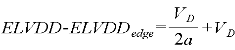
또한, 상기 비율 산출 단계에서는, 하기의 식을 이용하여 상기 비율을 산출할 수 있다.Further, in the ratio calculating step, the ratio can be calculated using the following equation.

ELVDD는 전원 전압, ELVDDcenter는 상기 전압 측정 단계에서 측정된 전압, VD는 상기 전원 전달 라인의 저항과 상기 전류 측정 단계에서 측정된 전류로 산출한 전압, a는 상기 비율을 의미한다.ELVDD denotes a power source voltage, ELVDDcenter denotes a voltage measured in the voltage measuring step, VD denotes a voltage calculated from the resistance of the power transmission line and the current measured in the current measuring step, and a denotes the ratio.
본 발명에 따른 유기 발광 표시 패널, 유기 발광 표시 장치 및 전압 강하 보상 방법은, 전원 전압 라인의 전압 강하로 인한 휘도 편차가 감소된 유기 발광 표시 패널, 유기 발광 표시 장치 및 전압 강하 보상 방법을 제공할 수 있다.The organic light emitting display panel, the organic light emitting display, and the voltage drop compensation method according to the present invention provide an organic light emitting display panel, an organic light emitting display, and a voltage drop compensation method in which a luminance deviation due to a voltage drop of a power supply voltage line is reduced .
도 1은 본 발명의 일 실시예에 따른 유기 발광 표시 장치의 구성을 개략적으로 나타내는 도면이다.
도 2는 본 발명의 일 실시예에 따른 표시 패널의 구성을 개략적으로 나타내는 도면이다.
도 3은 본 발명의 일 실시예에 픽셀의 구성을 예시적으로 나타내는 도면이다.
도 4는 전원 입력 라인 또는 전원 전달 라인 중 어느 하나를 통해서만 전원 전압을 인가하는 경우의 전압 강하를 나타내는 도면이다.
도 5는 본 발명의 일 실시예에 따른 유기 발광 표시 패널에서의 전압 강하를 개략적으로 나타내는 도면이다.
도 6은 본 발명의 일 실시예에 따른 유기 발광 표시 패널에서의 전압 강하를 보상하는 방법을 개략적으로 나타내는 도면이다.
도 7은 본 발명의 다른 실시예에 따른 유기 발광 표시 패널에서의 전압 강하를 보상하는 방법을 개략적으로 나타내는 도면이다.
도 8은 본 발명의 일 실시예에 따른 유기 발광 표시 패널의 전압 강하 보상 방법의 흐름을 개략적으로 나타내는 순서도이다.
도 9는 본 발명의 다른 실시예에 따른 유기 발광 표시 패널의 전압 강하 보상 방법의 흐름을 개략적으로 나타내는 순서도이다.1 is a view schematically showing a configuration of an organic light emitting display according to an embodiment of the present invention.
2 is a view schematically showing a configuration of a display panel according to an embodiment of the present invention.
3 is a diagram illustrating an exemplary configuration of a pixel according to an embodiment of the present invention.
4 is a graph showing a voltage drop when a power supply voltage is applied only through one of a power input line and a power supply line.
5 is a diagram schematically illustrating a voltage drop in an organic light emitting display panel according to an embodiment of the present invention.
6 is a diagram schematically illustrating a method of compensating a voltage drop in an organic light emitting display panel according to an embodiment of the present invention.
7 is a view schematically illustrating a method of compensating a voltage drop in an organic light emitting display panel according to another embodiment of the present invention.
8 is a flowchart schematically showing a flow of a voltage drop compensation method of an organic light emitting display panel according to an embodiment of the present invention.
9 is a flowchart schematically showing a flow of a voltage drop compensation method of an organic light emitting display panel according to another embodiment of the present invention.
본 발명은 다양한 변환을 가할 수 있고, 여러 가지 실시예들을 가질 수 있는 바, 특성 실시예들은 도면을 예시하고 상세한 설명에 상세하게 설명하고자 한다. 본 발명의 효과 및 특징, 그리고 그것들을 달성하는 방법은 도면과 함께 상세하게 후술되어 있는 실시예들을 참조하면 명확해질 것이다. 그러나 본 발명은 이하에서 개시되는 실시예들에 한정되는 것이 아니라 다양한 형태로 구현될 수 있다.The present invention is capable of various modifications and may have various embodiments, with specific embodiments being illustrative of the drawings and detailing in the detailed description. The effects and features of the present invention and methods of achieving them will be apparent with reference to the embodiments described in detail below with reference to the drawings. However, the present invention is not limited to the embodiments described below, but may be implemented in various forms.
이하 첨부된 도면들을 참조로 하여, 본 발명의 다양한 실시예에 따른 유기 발광 표시 패널, 유기 발광 표시 장치 및 전압 강하 보상 방법에 대해서 설명하도록 한다. 도면을 참조하여 설명할 때 동일하거나 대응하는 구성 요소는 동일한 도면 부호를 부여하고, 이에 대한 중복되는 설명은 생략하기로 한다.Hereinafter, an organic light emitting display panel, an organic light emitting display, and a voltage drop compensation method according to various embodiments of the present invention will be described with reference to the accompanying drawings. In the description with reference to the drawings, the same or corresponding components are denoted by the same reference numerals, and redundant description thereof will be omitted.
이하의 실시예에서, 제1, 제2 등의 용어는 한정적인 의미가 아니라 하나의 구성 요소를 다른 구성 요소와 구별하는 목적으로 사용된다. 단수의 표현은 문맥상 명확하게 다르게 뜻하지 않는 한, 복수의 표현을 의미한다. "포함하다" 또는 "가지다" 등의 용어는 명세서상에 기재된 특징 또는 구성 요소가 존재함을 의미하는 것이고, 하나 이상의 다른 특징들 또는 구성 요소가 부가될 가능성을 미리 배제하는 것은 아니다.
In the following embodiments, the terms first, second, etc. are used for the purpose of distinguishing one element from another element, rather than limiting. The singular expressions refer to plural expressions unless the context clearly dictates otherwise. The terms "comprises" or "having" mean that there is a feature or element recited in the specification and does not preclude the possibility that one or more other features or components may be added.
도 1은 본 발명의 일 실시예에 따른 유기 발광 표시 장치의 구성을 개략적으로 나타내는 도면이다.1 is a view schematically showing a configuration of an organic light emitting display according to an embodiment of the present invention.
도 1을 참조하면, 유기 발광 표시 장치(100)는, 표시 패널(110), 게이트 드라이버(120), 소스 드라이버(130), 제어부(140) 및 전원 전압 생성부(150)를 포함한다.Referring to FIG. 1, the
표시 패널(110)은, 복수의 픽셀(PX)들이 매트릭스로 배열되는 표시 영역(DA)을 포함한다. 픽셀(PX)들에는 제1 전원 전압(ELVDD)과 제2 전원 전압(ELVSS)이 인가된다. 제1 전원 전압(ELVDD)의 전압 레벨은 제2 전원 전압(ELVSS)의 전압 레벨보다 높다. 예컨대, 유기 발광 소자의 애노드에 제1 전원 전압(ELVDD)이 인가되고 캐소드에 제2 전원 전압(ELVSS)이 인가되면, 상기 유기 발광 소자는 발광한다. 제1 전원 전압(ELVDD) 및 제2 전원 전압(ELVSS)은 전원 전압 생성부(150)에서 생성된다.The
표시 패널(110)은, 픽셀(PX)들에 게이트 신호를 인가하는 게이트 라인들(GL1-GLn) 및 픽셀(PX)들에 소스 신호를 인가하는 소스 라인들(SL1-SLm)을 포함한다. 표시 패널(110)은 픽셀(PX)들에 제1 전원 전압(ELVDD)을 인가하기 위한 전원 배선 망을 포함한다. 게이트 라인들(GL1-GLn) 각각은 동일 행에 배열된 픽셀(PX)들에 연결되고, 소스 라인들(SL1-SLm) 각각은 동일 열에 배열된 픽셀(PX)들에 연결된다. 픽셀(PX)들은 게이트 라인들(GL1-GLn)을 통해 수신되는 게이트 신호에 응답하여 소스 라인들(SL1-SLm)을 통해 수신되는 데이터 신호의 논리 레벨에 따라 발광 또는 비발광한다. 이 경우, 표시 패널(110)은 디지털 구동 방식으로 동작한다. 다른 예에 따르면, 표시 패널(110)은 아날로그 구동 방식으로 동작할 수 있다. 이 경우, 픽셀(PX)들은 게이트 라인들(GL1-GLn)을 통해 수신되는 게이트 신호에 응답하여 소스 라인들(SL1-SLm)을 통해 수신되는 데이터 전압 레벨 또는 전류 레벨에 상응하는 밝기로 발광한다. 아래에서는 디지털 구동 방식으로 동작하는 유기 발광 표시 장치(100)를 중심으로 본 발명의 다양한 실시예들을 설명한다. 그러나, 본 발명은 디지털 구동 방식으로 동작하는 유기 발광 표시 장치뿐만 아니라, 아날로그 구동 방식으로 동작하는 유기 발광 표시 장치에도 적용될 수 있다는 것에 주의한다.The
본 발명의 일 실시예에 따르면, 도 1에 도시된 바와 같이, 상기 전원 배선 망은 제1 방향으로 연장되고, 제1 전원 전압(ELVDD)을 전달하는 전원 전달 라인(PTL), 상기 제1 방향으로 연장되고, 제1 전원 전압(ELVDD)이 인가되는 전원 입력 라인(PIL), 전원 전달 라인(PTL)로부터 전원 입력 라인(PIL)으로 제1 전원 전압(ELVDD)을 전달하는 연결부(CN), 표시 영역(DA) 바깥에서 제2 방향으로 연장되고, 전원 입력 라인(PIL)에 제1 전원 전압(ELVDD)을 공급하는 제1 및 제2 전원 배선(power wire)(PW1, PW2)을 포함할 수 있다.1, the power supply wiring network includes a power supply line PTL extending in a first direction and transmitting a first power supply voltage ELVDD, And includes a power supply input line PIL to which the first power supply voltage ELVDD is applied, a connection portion CN to transmit the first power supply voltage ELVDD from the power supply line PTL to the power supply input line PIL, And first and second power wires PW1 and PW2 that extend in a second direction outside the display area DA and supply a first power source voltage ELVDD to the power source input line PIL .
전원 배선(PW1, PW2)은 전원 입력 라인(PIL)이 연장되는 제1 방향과 수직으로 만나는 제2 방향으로 표시 영역(DA) 바깥에 배치될 수 있으며, 전원 전압 생성부(150)에서 생성된 제1 전원 전압(ELVDD)이 직접 인가될 수 있다. 전원 배선(PW1, PW2)은 전원 입력 라인(PIL)에 비해 낮은 선 저항을 갖기 때문에, 전류의 흐름에 따른 전압 강하는 무시할 수 있을 정도로 작을 수 있다. 도 1에서 제1 전원 배선(PW1)은 표시 영역(DA)의 상단에 배치되고, 제2 전원 배선(PW2)은 표시 영역(DA)의 하단에 배치되는 것으로 도시되지만, 설계에 따라서 표시 영역(DA)의 좌측 및/또는 우측에 전원 배선이 배치되거나, 표시 영역(DA)을 둘러싸도록 전원 배선이 배치될 수도 있다.The power supply lines PW1 and PW2 may be disposed outside the display area DA in a second direction perpendicular to the first direction in which the power supply input line PIL extends, The first power supply voltage ELVDD may be directly applied. Since the power supply lines PW1 and PW2 have a lower line resistance than the power supply input line PIL, the voltage drop along the current flow can be negligibly small. 1, the first power supply line PW1 is arranged at the upper end of the display area DA and the second power supply line PW2 is arranged at the lower end of the display area DA, DA may be disposed on the left and / or right side of the display area DA, or the power supply wiring may be disposed so as to surround the display area DA.
도 1에는 하나의 전원 입력 라인(PIL)만이 도시되었지만, 표시 패널(110) 상에는 복수의 전원 입력 라인(PIL)들이 배열되고, 전원 입력 라인(PIL)들은 제1 및 제2 전원 배선들(PW1, PW2) 중 적어도 하나에 연결될 수 있다. 도 1에 도시된 바와 같이, 전원 입력 라인(PIL)들은 제1 및 제2 전원 배선(PW1, PW2) 사이에 연결될 수 있다. 전원 입력 라인(PIL)들 각각은 제1 전원 배선(PW1)에 연결되는 제1 단부와 제2 전원 배선(PW2)에 연결되는 제2 단부를 갖는다. 제1 및 제2 전원 배선(PW1, PW2) 중 하나가 생략된 경우, 전원 입력 라인(PIL)은 나머지 전원 배선에 연결된다. 전원 배선이 표시 영역(DA)의 좌측 및/또는 우측에 배치되는 경우, 전원 입력 라인(PIL)은 행 방향(도 1에서 가로 방향)으로 연장될 수 있으며, 전원 배선이 표시 영역(DA)을 둘러싸도록 배치되는 경우, 전원 입력 라인(PIL)들은 메쉬(mesh) 형태로 배열될 수 있다. 전원 입력 라인(PIL)은 표시 영역(DA) 상의 첫 번째 행의 픽셀에서부터 마지막 행의 픽셀까지의 픽셀(PX)들에 모두 연결되기 위하여, 표시 영역(DA) 전체를 가로질러 배치되며, 전원 배선들(PW1, PW2)에 직접 연결된다.Although only one power input line PIL is shown in FIG. 1, a plurality of power input lines PIL are arranged on the
도 1에는 하나의 전원 전달 라인(PTL)만이 도시되었지만, 표시 패널(110) 상에는 복수의 전원 전달 라인(PLT)들이 배열되며, 복수의 전원 전달 라인(PTL)들은 전원 입력 라인(PIL)과 달리 픽셀(PX)들에 직접 연결되지 않는다. 도 1에 도시된 바와 같이, 전원 전달 라인(PTL)들은 열 방향(도 1에서 세로 방향)으로 연장될 수 있다. 전원 전달 라인(PTL)들은 행 방향으로 연장되거나, 메쉬 형태로 배열될 수도 있다. 전원 전달 라인(PTL)은 표시 영역(DA) 전체를 가로질러 배치되며, 전원 배선들(PW1, PW2)에 직접 연결된다.Although only one power supply line PTL is shown in FIG. 1, a plurality of power supply lines PLT are arranged on the
연결부(CN)는 전원 입력 라인(PIL)과 전원 전달 라인(PTL)을 서로 전기적으로 연결한다. 연결부(CN)는 전원 전달 라인(PTL)과 전원 입력 라인(PIL)의 중간 부분에 연결될 수 있다. 본 명세서에서 전원 입력 라인(PIL) 의 중간 부분은 각각 전원 입력 라인(PIL) 의 길이 방향을 따라 전원 전달 라인(PTL)의 중앙점에 인접한 부분들을 지칭한다.The connection part CN electrically connects the power input line PIL and the power supply line PTL with each other. The connection portion CN may be connected to an intermediate portion between the power supply line PTL and the power supply line PIL. In this specification, the middle portion of the power input line PIL refers to portions adjacent to the center point of the power supply line PTL along the longitudinal direction of the power supply input line PIL.
도 1에 도시된 실시예에 따르면, 전원 전압 생성부(150)에 의해 생성된 제1 전원 전압(ELVDD)은 제1 및 제2 전원 배선(PW1, PW2)에 인가되고, 전원 입력 라인(PIL)을 통해 픽셀(PX)들에 인가된다. 또는, 제1 전원 전압(ELVDD)은 제1 및 제2 전원 배선(PW1, PW2)에 인가되고, 전원 전달 라인(PTL), 연결부(CN) 및 전원 입력 라인(PIL)을 통해 픽셀(PX)들에 인가된다. 따라서, 전원 입력 라인(PIL)에 흐르는 전류(I)는 제1 배선(PW1) 및 제2 배선(PW2)으로부터 전원 입력 라인(PIL)의 중앙점을 향해 흐르게 된다. 그리고, 전원 전달 라인(PTL)에 흐르는 전류(I)는 제1 전원 배선(PW1) 및 제2 전원 배선(PW2)으로부터 연결부(CN)를 거쳐 전원 입력 라인(PIL)의 중앙점에서 제1 전원 배선(PW1) 또는 제2 전원 배선(PW2)을 향해 흐르게 된다. 전원 전달 라인(PTL) 및 전원 입력 라인(PIL)은 저항 성분을 가지므로, 전원 전달 라인(PTL) 및 전원 입력 라인(PIL)을 따라 흐르는 전류에 의하여 전압 강하가 발생한다. 전압 강하로 인하여, 전원 입력 라인(PIL)에 연결되는 복수의 픽셀(PX)들 중에서 제1 전원 배선(PW1)에 가장 가까이 배치되는 픽셀(PX1) 또는 제2 전원 배선(PW2)에 가장 가까이 배치되는 픽셀(PX3)에 인가되는 전압 레벨은 연결부(CN)와 가장 가까이 배치되는 픽셀(PX2, PX4)에 인가되는 전압 레벨보다 높다.1, the first power source voltage ELVDD generated by the power
전원 전압 생성부(150)에 의해 생성된 제2 전원 전압(ELVSS)은 공통 전극을 통해 픽셀(PX)들에 인가된다. 상기 공통 전극은 픽셀(PX)들의 발광 소자의 일 전극(예컨대, 캐소드 전극)에 대응할 수 있으며, 픽셀(PX)들은 모두 상기 공통 전극에 연결된다. 상기 공통 전극은 표시 영역(DA) 상의 픽셀(PX)들을 덮도록 전면적으로 형성될 수 있으며, 제2 전원 전압(ELVSS)은 표시 영역(DA)의 외곽으로부터 상기 공통 전극에 인가될 수 있다. 제2 전원 전압(ELVSS)은 제1 전원 전압(ELVDD)보다 전압 레벨이 낮기 때문에, 픽셀(PX)들에 공급된 전류는 상기 공통 전극을 통해 전압 전원 생성부(150)로 빠져나간다. 따라서, 제2 전원 전압(ELVSS)이 인가되는 상기 공통 전극의 외곽부의 전압 레벨은 상기 공통 전극의 중앙부의 전압 레벨보다 낮다. 즉, 상기 공통 전극의 중앙부에서 상기 공통 전극의 외곽부로 전류가 흐른다.The second power supply voltage ELVSS generated by the power supply
도 1의 실시예에 제시된 제1 전원 전압(ELVDD)과 같이, 제2 전원 전압(ELVSS)은 표시 영역(DA)의 상단 및 하단으로부터 상기 공통 전극에 인가될 수 있다. 그러나, 본 발명은 이에 한정되지 않으며, 설계에 따라서 제2 전원 전압(ELVSS)은 표시 영역(DA)의 상단, 하단, 좌측 및 우측 중 적어도 하나로부터 상기 공통 전극에 인가될 수 있다.
The second power source voltage ELVSS may be applied to the common electrode from the upper and lower ends of the display area DA as in the first power source voltage ELVDD shown in the embodiment of FIG. However, the present invention is not limited to this, and the second power supply voltage ELVSS may be applied to the common electrode from at least one of the top, bottom, left, and right sides of the display area DA according to the design.
도 2는 본 발명의 일 실시예에 따른 표시 패널의 구성을 개략적으로 나타내는 도면이다.2 is a view schematically showing a configuration of a display panel according to an embodiment of the present invention.
도 2에 도시되는 표시 패널(110)은 도 1을 참조로 하여 설명한 유기 발광 표시 장치(100)에 포함되는 표시 패널(110)을 보다 구체적으로 도시한 것이다. 도 2를 참조하면, 표시 패널(110)은 전원 입력 라인(PIL), 전원 전달 라인(PTL), 제1 및 제2 전원 배선(PW1, PW2)을 포함한다. 또한, 표시 패널(110)은 전원 전압을 공급받아 발광하는 유기 발광 소자(OLED) 및 유기 발광 소자(OLED)에 전원 전압을 공급하는 적어도 하나 이상의 박막 트랜지스터(TFT)를 포함한다.The
전원 전달 라인(PTL)은 제1 방향으로 연장되고, 제1 전원 배선(PW1) 및 제2 전원 배선(PW2)으로부터 제1 전원 전압(ELVDD)을 공급받는다. 그리고, 전원 전달 라인(PTL)은 연결부(CN)를 통해 전원 입력 라인(PIL)의 가운데 지점에 연결되어 제1 전원 전압(ELVDD)을 전원 전달 라인(ELVDD)으로 전달한다. 도 2에 도시되는 바와 같이, 전원 전달 라인(PTL)은 복수 개가 있을 수 있으며, 전원 전달 라인(PTL)의 개수는 전체 픽셀의 개수, 표시 패널(110)의 크기에 따라 달라질 수 있음은 자명하다.The power supply line PTL extends in the first direction and receives the first power supply voltage ELVDD from the first power supply line PW1 and the second power supply line PW2. The power supply line PTL is connected to the center point of the power supply input line PIL through the connection part CN and transfers the first power supply voltage ELVDD to the power supply line ELVDD. 2, it is obvious that there may be a plurality of power transmission lines PTL and that the number of power transmission lines PTL may vary depending on the total number of pixels and the size of the
전원 입력 라인(PIL)은 전원 전달 라인(PTL)과 같이 제1 방향으로 연장되고, 제1 전원 배선(PW1) 및 제2 전원 배선(PW2)로부터 제1 전원 전압(ELVDD)을 공급 받는다. 그리고, 전원 입력 라인(PIL)은 가운데 지점에서 전원 전달 라인(PTL)과 연결되어 전원 전달 라인(PTL)으로부터 제1 전원 전압(ELVDD)을 전달 받는다.The power input line PIL extends in the first direction like the power supply line PTL and receives the first power supply voltage ELVDD from the first power supply line PW1 and the second power supply line PW2. The power supply line PIL is connected to the power supply line PTL at the center and receives the first power supply voltage ELVDD from the power supply line PTL.
제1 전원 배선(PW1) 및 제2 전원 배선(PW2)은 제2 방향으로 연장되고, 전원 전압 생성부(150)와 연결되어 제1 전원 전압(ELVDD)을 공급 받는다. 제1 전원 배선(PW1) 및 제2 전원 배선(PW2)은 전원 전달 라인(PTL) 및 전원 입력 라인(PIL)과 직접 연결되어 전원 전달 라인(PTL) 및 전원 입력 라인(PIL)에 제1 전원 전압(ELVDD)을 공급한다.The first power supply line PW1 and the second power supply line PW2 extend in the second direction and are connected to the power supply
전원 입력 라인(PIL)에 인가되는 제1 전원 전압(ELVDD)에 의해 전원 입력 라인(PIL)을 통해 흐르는 전류는 복수의 픽셀(PX)들로 흐르고, 픽셀(PX)에 공급된 전류는 박막 트랜지스터(TFT)를 포함하는 픽셀 회로와 유기 발광 소자(OLED)의 애노드(Anode) 및 캐소드(Cathode)를 통해 흐르게 된다.The current flowing through the power supply input line PIL flows to the plurality of pixels PX by the first power supply voltage ELVDD applied to the power supply input line PIL, (TFT), and an anode and a cathode of the organic light emitting diode OLED.
복수의 픽셀(PX)들은 전원 입력 라인(PIL)에 직접 연결되어 제1 전원 전압(ELVDD)을 공급 받으며, 도 2에 도시되는 바와 같이 전원 전달 라인(PTL)에는 직접 연결되지 않는다. 복수의 픽셀(PX)들은 전원 입력 라인(PIL)에 연결되는 위치에 따라 제1 전원 배선(PW1) 또는 제2 전원 배선(PW2)으로부터 전원 입력 라인(PIL)에 직접 공급되는 제1 전원 전압(ELVDD)을 공급 받을 수 있다. 또는, 복수의 픽셀(PX)들은 전원 입력 라인(PIL)에 연결되는 위치에 따라 제1 전원 배선(PW1) 또는 제2 전원 배선(PW2)으로부터 전원 전달 라인(PTL), 연결부(CN) 및 전원 입력 라인(PIL)을 통해 전달되는 제1 전원 전압(ELVDD)을 공급 받을 수 있다. 따라서, 복수의 픽셀(PX)들에 공급되는 제1 전원 전압(ELVDD)의 크기는 각각의 픽셀(PX)마다 다를 수 있다. 예컨대, 제1 전원 배선(PW1) 또는 제2 전원 배선(PW2)에 가까이 배치되는 픽셀(PX)에 공급되는 제1 전원 전압(ELVDD)의 크기는 연결부(CN)에 가까이 배치되는 픽셀(PX)에 공급되는 제1 전원 전압(ELVDD)의 크기보다 클 수 있다. 제1 전원 배선(PW1) 또는 제2 전원 배선(PW2)에 가까이 배치되는 픽셀(PX)에는 제1 전원 배선(PW1) 또는 제2 전원 배선(PW2)으로부터 전원 입력 라인(PIL)을 통해 제1 전원 전압(ELVDD)이 공급되는 반면, 연결부(CN)에 가까이 배치되는 픽셀(PX)에 공급되는 제1 전원 전압(ELVDD)은 제1 전원 배선(PW1) 또는 제2 전원 배선(PW2)으로부터 전원 전달 라인(PTL), 연결부(CN) 및 전원 입력 라인(PIL)을 거쳐 공급되기 때문이다. 즉, 전원 전달 라인(PTL), 전원 입력 라인(PIL) 및 연결부(CN)의 저항 성분으로 인한 전압 강하가 발생하여 픽셀(PX)이 배치되는 위치에 따라 제1 전원 전압(ELVDD)의 레벨이 달라지게 된다.The plurality of pixels PX are directly connected to the power supply input line PIL and are supplied with the first power supply voltage ELVDD and are not directly connected to the power supply line PTL as shown in FIG. The plurality of pixels PX are connected to the first power supply line PW1 or the first power supply voltage PIL directly supplied from the second power supply line PW2 to the power supply line PIL depending on the position connected to the power supply input line PIL ELVDD). Alternatively, the plurality of pixels PX may be connected to the power supply line PTL, the connection portion CN, and the power supply line POL from the first power supply line PW1 or the second power supply line PW2, depending on the position connected to the power supply input line PIL. And can receive the first power supply voltage ELVDD transmitted through the input line PIL. Therefore, the magnitude of the first power supply voltage ELVDD supplied to the plurality of pixels PX may be different for each pixel PX. For example, the magnitude of the first power supply voltage ELVDD supplied to the pixel PX disposed close to the first power supply wiring PW1 or the second power supply wiring PW2 is the same as that of the pixel PX disposed close to the connection portion CN. The first power supply voltage ELVDD may be greater than the first power supply voltage ELVDD. The pixel PX disposed close to the first power supply line PW1 or the second power supply line PW2 is connected to the first power supply line PW1 or the second power supply line PW2 through the power supply input line PIL, The first power supply voltage ELVDD supplied to the pixel PX disposed close to the connection part CN is supplied from the first power supply line PW1 or the second power supply line PW2 to the power supply line ELVDD, The supply line PTL, the connection CN and the power input line PIL. That is, a voltage drop due to a resistance component of the power supply line PTL, the power supply input line PIL, and the connection portion CN occurs and the level of the first power supply voltage ELVDD varies depending on the position of the pixel PX Will be different.
도 2에서 전원 입력 라인(PIL)에 연결되는 제1 전원 배선(PW1)과 전원 전달 라인(PTL)에 연결되는 제1 전원 배선(PW1)은 별도로 도시되어 있으나, 제1 전원 배선(PW1)은 전원 입력 라인(PIL)과 전원 전달 라인(PTL)에 동시에 연결되며 실질적으로 동일한 배선으로 이해할 수 있다. 전원 입력 라인(PIL)에 연결되는 제2 전원 배선(PW2)과 전원 전달 라인(PTL)에 연결되는 제2 전원 배선(PW2) 역시 별도로 도시되어 있으나, 제2 전원 배선(PW2)은 전원 입력 라인(PIL)과 전원 전달 라인(PTL)에 동시에 연결되는 실질적으로 동일한 배선으로 이해할 수 있다.The first power supply line PW1 connected to the power input line PIL and the first power supply line PW1 connected to the power supply line PTL are separately shown in FIG. It can be understood that they are connected to the power input line (PIL) and the power transmission line (PTL) at the same time and substantially the same wiring. The second power supply line PW2 connected to the power supply input line PIL and the second power supply line PW2 connected to the power supply line PTL are also separately shown, Can be understood as substantially the same wiring which is simultaneously connected to the power supply line (PIL) and the power supply transmission line (PTL).
도 2에서 캐소드(Cathode)는 픽셀(PX)을 흐르는 전류가 출력되는 전극일 수 있으며, 복수의 픽셀(PX)들을 모두 덮도록 공통 전극으로 형성될 수 있다. 그리고, 캐소드(Cathode) 전극에는 전원 전압 생성부(150)에서 생성된 제2 전원 전압(ELVSS)이 인가될 수 있다.In FIG. 2, a cathode may be an electrode through which a current flowing through the pixel PX is output, and may be formed as a common electrode to cover all of the plurality of pixels PX. The second power supply voltage ELVSS generated by the power
제1 전원 배선(PW1)과 제2 전원 배선(PW2)은 표시 패널(110)의 표시 영역 외부에 형성되고, 전원 입력 라인(PIL)과 전원 전달 라인(PTL)은 일부가 표시 영역 내부에 형성되고 나머지 일부는 표시 영역 외부에 형성된다. 또한, 표시 영역은 복수의 픽셀(PX)들을 포함할 수 있다.The first power supply line PW1 and the second power supply line PW2 are formed outside the display region of the
도 2에 도시되는 바와 같이, 복수의 전원 입력 라인(PIL)들 및 복수의 전원 전달 라인(PTL)들에는 제1 전원 배선(PW1) 및 제2 전원 배선(PW2)로부터 제1 전원 전압(ELVDD)이 인가되며, 제1 전원 배선(PW1) 및 제2 전원 배선(PW2)의 길이 방향에 따라 발생하는 전압 강하는 무시할 수 있을 정도로 작을 수 있다. 따라서, 제1 전원 배선(PW1) 및 제2 전원 배선(PW2)에 인가되는 전압은 길이 방향을 따라 모두 동일하며, 전원 입력 라인(PIL)들 및 전원 전달 라인(PTL)에 인가되는 제1 전원 전압(ELVDD)의 레벨은 위치에 관계없이 모두 동일하다.
2, the first power supply line PW1 and the second power supply line PW2 are supplied with a first power supply voltage ELVDD (second power supply voltage) from the power supply lines PIL and the plurality of power supply lines PTL, And the voltage drop occurring along the length direction of the first power supply line PW1 and the second power supply line PW2 can be negligibly small. Therefore, the voltages applied to the first power supply line PW1 and the second power supply line PW2 are all the same along the longitudinal direction, and the voltages applied to the power supply lines PIL and the power supply line PTL, The level of the voltage ELVDD is the same regardless of the position.
도 3은 본 발명의 일 실시예에 픽셀의 구성을 예시적으로 나타내는 도면이다.3 is a diagram illustrating an exemplary configuration of a pixel according to an embodiment of the present invention.
도 3을 참조하면, 픽셀(PX)은 동일 행의 게이트 라인(GL) 및 동일 열의 소스 라인(SL)에 연결된다. 픽셀(PX)은 제1 트랜지스터(M1), 제2 트랜지스터(M2), 및 저장 커패시터(Cst)를 포함하는 픽셀 회로, 및 유기 발광 소자(OLED)를 포함하는 발광 소자를 포함한다. 제1 및 제2 트랜지스터(M1, M2)는 박막 트랜지스터일 수 있다. 제1 트랜지스터(M1)는 소스 라인(SL)에 연결된 제1 연결 단자, 노드(Nd)에 연결된 제2 단자, 및 게이트 라인(GL)에 연결된 제어 단자를 포함한다. 제2 트랜지스터(M2)는 제1 전원 전압(ELVDD)이 인가되는 전원 입력 라인(PIL)에 연결된 제1 연결 단자, 노드(Nd)에 연결된 제어 단자, 및 유기 발광 소자(OLED)의 제1 전극에 연결된 제2 연결 단자를 포함한다. 저장 커패시터(Cst)는 제2 트랜지스터(M2)의 제1 연결 단자에 연결된 제1 단자, 및 노드(Nd)에 연결된 제2 단자를 포함한다. 유기 발광 소자(OLED)는 제2 트랜지스터(M2)의 제2 연결 단자에 연결된 제1 전극 및 제2 전원 전압(ELVSS)이 인가되는 공통 전극(CE)에 연결되는 제2 전극을 포함한다. 유기 발광 소자(OLED)의 제1 전극 및 제2 전극은 각각 애노드 전극 및 캐소드 전극일 수 있다.Referring to Fig. 3, the pixel PX is connected to the gate line GL in the same row and the source line SL in the same column. The pixel PX includes a pixel circuit including a first transistor M1, a second transistor M2, and a storage capacitor Cst, and a light emitting element including an organic light emitting diode OLED. The first and second transistors M1 and M2 may be thin film transistors. The first transistor M1 includes a first connection terminal connected to the source line SL, a second terminal connected to the node Nd and a control terminal connected to the gate line GL. The second transistor M2 includes a first connection terminal connected to the power supply input line PIL to which the first power supply voltage ELVDD is applied, a control terminal connected to the node Nd, And a second connection terminal connected to the second connection terminal. The storage capacitor Cst includes a first terminal connected to the first connection terminal of the second transistor M2 and a second terminal connected to the node Nd. The organic light emitting diode OLED includes a first electrode connected to the second connection terminal of the second transistor M2 and a second electrode connected to the common electrode CE to which the second power supply voltage ELVSS is applied. The first electrode and the second electrode of the organic light emitting diode OLED may be an anode electrode and a cathode electrode, respectively.
픽셀(PX)은 게이트 라인(GL)을 통해 스캔 신호(S)를 수신하고, 소스 라인(SL)을 통해 데이터 신호(D)를 수신한다. 제1 트랜지스터(M1)는 스캔 신호(S)에 응답하여 데이터 신호(D)를 제2 트랜지스터(M2)의 제어 단자에 전달한다. 제2 트랜지스터(M2)는 전달된 데이터 신호(D)의 논리 레벨에 따라 턴 온 또는 턴 오프되며, 제2 트랜지스터(M2)가 턴 온되면, 제1 전원 전압(ELVDD)을 유기 발광 소자(OLED)의 제1 전극에 전달한다. 저장 커패시터(Cst)는 데이터 신호(D)의 논리 레벨에 따른 제2 트랜지스터(M2)의 턴 온 상태 또는 턴 오프 상태를 서브필드 시구간 동안 유지한다. 예컨대, 디지털 데이터 신호(D)가 제1 논리 레벨을 갖는 경우, 유기 발광 소자(OLED)의 제1 전극에는 제1 전원 전압(ELVDD)이 인가되며, 유기 발광 소자(OLED)는 발광한다. 디지털 데이터 신호(D)가 제2 논리 레벨을 갖는 경우, 제2 트랜지스터(M2)가 턴 오프되어 유기 발광 소자(OLED)의 제1 전극에는 제1 전원 전압(ELVDD)이 인가되지 않으며, 유기 발광 소자(OLED)는 발광하지 않는다.The pixel PX receives the scan signal S through the gate line GL and the data signal D through the source line SL. The first transistor M1 responds to the scan signal S and transmits the data signal D to the control terminal of the second transistor M2. The second transistor M2 is turned on or off according to the logic level of the transferred data signal D and the first power source voltage ELVDD is applied to the organic light emitting diode OLED To the first electrode of the plasma display panel. The storage capacitor Cst maintains the turn-on or turn-off state of the second transistor M2 for the subfield time period according to the logic level of the data signal D. For example, when the digital data signal D has the first logic level, the first power source voltage ELVDD is applied to the first electrode of the organic light emitting device OLED, and the organic light emitting device OLED emits light. When the digital data signal D has the second logic level, the second transistor M2 is turned off so that the first power source voltage ELVDD is not applied to the first electrode of the organic light emitting device OLED, The element OLED does not emit light.
도 3에 도시된 픽셀(PX)의 회로 구성은 오로지 예시적이며, 픽셀(PX)은 다른 회로 구성을 가질 수 있다.
The circuit configuration of the pixel PX shown in Fig. 3 is only exemplary, and the pixel PX may have a different circuit configuration.
도 4는 전원 입력 라인 또는 전원 전달 라인 중 어느 하나를 통해서만 전원 전압을 인가하는 경우의 전압 강하를 나타내는 도면이다.4 is a graph showing a voltage drop when a power supply voltage is applied only through one of a power input line and a power supply line.
도 4에서 패널 엣지(Panel Edge)는 제1 전원 배선(PW1) 또는 제2 전원 배선(PW2)이 배치되는 위치를 나타내고, 패널 센터(Panel Center)는 제1 전원 배선(PW1)과 제2 전원 배선(PW2)의 중앙 지점을 나타낸다. 패널 엣지(Panel Edge)는 전원 전압 생성부(150)에서 생성된 전원 전압이 제1 전원 배선(PW1) 또는 제2 전원 배선(PW2)을 통하여 직접 공급되는 위치이므로 표시 패널(110)에 공급되는 전원 전압 중 가장 높은 전압 레벨을 갖게 된다. 여기서 전원 전압은 제1 전원 전압(ELVDD)을 의미한다.4, the panel edge represents a position where the first power supply line PW1 or the second power supply line PW2 is disposed, and the panel center is connected to the first power supply line PW1 and the second power supply line PW2. And the center point of the wiring PW2. The panel edge is a position where the power supply voltage generated by the power supply
도 4(a)는 도 1 및 도 2를 참조로 하여 설명한 바와 같은 표시 패널(110)의 전원 전달 라인(PTL)을 통해서만 전원 전압을 인가하는 경우의 전압 강하를 나타낸다. 전원 전달 라인(PTL)을 통해서만 전원 전압을 인가하는 경우에는 전원 전달 라인(PTL), 연결부(CN) 및 전원 입력 라인(PIL)을 통해 제1 전원 전압(ELVDD)이 인가되므로 전원 입력 라인(PIL)에 연결된 픽셀(PX)들 중에서 제1 전원 배선(PW1) 또는 제2 전원 배선(PW2) 가까이에 연결되는 픽셀(PX)에는 전압 강하로 인해 상대적으로 낮은 레벨의 제1 전원 전압(ELVDD)이 인가될 수 있다.4 (a) shows a voltage drop when the power supply voltage is applied only through the power supply transmission line PTL of the
한편, 도 4에서 ELVDDedge는 복수의 픽셀(PX)들 중에서 제1 전원 배선(PW1) 또는 제2 전원 배선(PW2)에 가장 가까이에 배치되는 픽셀(PX)에 공급되는 제1 전원 전압을 나타낸다.On the other hand, in FIG. 4, the ELVDD edge represents the first power supply voltage supplied to the pixel PX disposed closest to the first power supply line PW1 or the second power supply line PW2 among the plurality of pixels PX .
제1 전원 배선(PW1) 또는 제2 전원 배선(PW2)을 통해 공급된 제1 전원 전압(ELVDD)은 전원 전달 라인(PTL)을 통해 전원 입력 라인(PIL)의 가운데 지점에 연결된 연결부(CN)로 전달되는 동안 전원 전달 라인(PTL)의 저항 성분으로 인해 레벨이 점점 감소한다. 그리고, 연결부(CN)를 통해 전원 입력 라인(PIL)으로 공급된 제1 전원 전압은 전원 입력 라인(PIL)의 가운데 지점에서 길이 방향을 따라 복수의 픽셀(PX)들로 공급되면서 계속 감소한다. 이때, 전원 입력 라인(PIL)을 통해 공급되는 제1 전원 전압의 크기는 전원 입력 라인(PIL)에 연결되는 픽셀 회로 및 유기 발광 소자의 저항 성분으로 인해 비선형적으로 감소할 수 있다.The first power supply voltage ELVDD supplied through the first power supply line PW1 or the second power supply line PW2 is connected to the connection point CN connected to the center point of the power supply input line PIL through the power supply line PTL, The level is gradually reduced due to the resistance component of the power supply line PTL. The first power supply voltage supplied to the power supply input line PIL through the connection part CN is continuously supplied while being supplied to the plurality of pixels PX along the longitudinal direction at the center point of the power supply input line PIL. At this time, the magnitude of the first power supply voltage supplied through the power supply input line (PIL) may decrease non-linearly due to the resistance component of the pixel circuit and the organic light emitting diode connected to the power supply input line (PIL).
도 4(a)에서 표시 패널(110)에서 발생하는 전압 강하의 크기는 ELVDD-ELVDDedge로 정의할 수 있다.The magnitude of the voltage drop occurring in the
도 4(b)는 도 1 및 도 2를 참조로 하여 설명한 바와 같은 표시 패널(110)의 전원 입력 라인(PIL)을 통해서만 전원 전압을 인가하는 경우의 전압 강하를 나타낸다. 전원 입력 라인(PIL)을 통해서만 전원 전압을 인가하는 경우에는 전원 전달 라인(PTL) 및 연결부(CN)를 통해 제1 전원 전압(ELVDD)이 인가되지 않으므로 전원 입력 라인(PIL)에 연결된 픽셀(PX)들 중에서 연결부(CN) 가까이에 연결되는 픽셀(PX)에는 전압 강하로 인해 상대적으로 낮은 레벨의 제1 전원 전압(ELVDD)이 인가될 수 있다.4 (b) shows a voltage drop when the power supply voltage is applied only through the power supply input line PIL of the
제1 전원 배선(PW1) 또는 제2 전원 배선(PW2)을 통해 공급된 제1 전원 전압(ELVDD)은 전원 입력 라인(PIL)을 통해 전달되는 동안 전원 입력 라인(PIL)의 저항 성분으로 인해 레벨이 점점 감소한다. 그리고, 전원 입력 라인(PIL)을 통해 공급되는 제1 전원 전압의 크기는 전원 입력 라인(PIL)에 연결되는 픽셀 회로 및 유기 발광 소자의 저항 성분으로 인해 비선형적으로 감소할 수 있다.The first power supply voltage ELVDD supplied through the first power supply line PW1 or the second power supply line PW2 is leveled due to the resistance component of the power supply input line PIL while being transmitted through the power supply input line PIL. Is gradually decreasing. The size of the first power supply voltage supplied through the power supply line PIL may be reduced non-linearly due to the resistance component of the pixel circuit and the organic light emitting diode connected to the power supply input line PIL.
도 4(b)에서 표시 패널(110)에서 발생하는 전압 강하의 크기는 ELVDD-ELVDDcenter로 정의할 수 있으며, 여기서 ELVDDcenter는 연결부(CN)에 인가되는 전압의 크기를 나타낸다.In FIG. 4 (b), the magnitude of the voltage drop generated in the
한편, 전원 입력 라인(PIL)을 통해서만 제1 전원 전압(ELVDD)이 공급되는 경우에는 전원 전달 라인(PTL)으로 흐르는 전류는 발생하지 않으므로 전원 전달 라인(PTL)에 의한 전압 강하 효과는 고려하지 않아도 무방하다.
On the other hand, when the first power supply voltage ELVDD is supplied only through the power supply input line PIL, no current flows to the power supply line PTL, so that the voltage drop effect by the power supply line PTL is not considered It is acceptable.
도 5는 본 발명의 일 실시예에 따른 유기 발광 표시 패널에서의 전압 강하를 개략적으로 나타내는 도면이다.5 is a diagram schematically illustrating a voltage drop in an organic light emitting display panel according to an embodiment of the present invention.
도 1 및 도 2를 참조로 하여 설명한 바와 같이, 본 발명의 일 실시예에 따른 표시 패널(110)에서는 전원 입력 라인(PIL)과 전원 전달 라인(PTL)이 모두 제1 전원 배선(PW1) 또는 제2 전원 배선(PW2)에 연결되어 제1 전원 전압(ELVDD)을 공급받을 수 있다. 도 5를 참조하면, 전원 전달 라인(PTL)을 통해 공급되는 제1 전원 전압(ELVDD)의 크기는 패널 엣지(Panel Edge)로부터 패널 센터(Panel Center)를 향하는 동안 전원 전달 라인(PTL)의 저항 성분에 의해 선형적으로 감소하게 된다. 그리고, 전원 전달 라인(PTL), 연결부(CN) 및 전원 입력 라인(PIL)을 통해 픽셀(PX)로 공급되는 제1 전원 전압(ELVDD)의 크기는 전원 입력 라인(PIL)의 가운데 지점, 즉 연결부(CN)로부터 전원 입력 라인(PIL)의 길이 방향을 따라 감소하게 된다. 다만, 전원 입력 라인(PIL)은 전원 전달 라인(PTL)뿐만 아니라 제1 전원 배선(PW1) 또는 제2 전원 배선(PW2)으로부터 제1 전원 전압(ELVDD)을 공급 받기 때문에 전원 입력 라인(PIL)을 통해 공급되는 제1 전원 전압(ELVDD)의 크기는 패널 엣지(Panel Edge)를 향하면서 다시 증가하게 된다.1 and 2, in the
도 5에서 표시 패널(110)에서 발생하는 전압 강하의 크기는 ELVDD-ELVDDmin으로 정의할 수 있으며, 여기서 ELVDDmin이 되는 위치는 하기 수학식에 의해 계산될 수 있다.The magnitude of the voltage drop occurring in the

여기서, L은 패널 센터로부터 패널 엣지까지의 거리, a는 전원 입력 라인의 저항 값에 대한 전원 전달 라인의 저항 값의 비율을 의미한다.Here, L is the distance from the panel center to the panel edge, and a is the ratio of the resistance value of the power transmission line to the resistance value of the power input line.
도 5는 전원 입력 라인의 저항 값과 전원 전달 라인의 저항 값이 같은 경우, 즉 a 값이 1인 경우를 도시하며, 공급되는 제1 전원 전압(ELVDD)의 크기가 가장 작게(ELVDDmin) 되는 위치는 L/4가 된다.
FIG. 5 shows a case where the resistance value of the power supply input line is equal to the resistance value of the power supply line, that is, the value of a is 1. When the supplied first power supply voltage ELVDD is the smallest (ELVDD min ) The position becomes L / 4.
한편, 도 4(a)와 같이 전원 전달 라인(PTL)만을 통해 제1 전원 전압(ELVDD)을 공급하는 경우에 ELVDD-ELVDDcenter 값을 VD로 정의하면, ELVDDcenter-ELVDDedge 값은 VD/2로 계산된다. 따라서, 도 4(a)에서 전압 강하는 3VD/2가 된다.4A, when the ELVDD-ELVDD center value is defined as V D when the first power voltage ELVDD is supplied only through the power supply line PTL, the ELVDD center -ELVDD edge value is V D / 2. Therefore, the voltage drop in FIG. 4A becomes 3V D / 2.
그리고, 도 5와 같이 본 발명의 일 실시예에 따른 표시 패널(110)에서의 전압 강하는 9VD/32로 계산되며, 도 4(a)와 같은 경우에 비하여 대략 19% 정도의 전압 강하를 갖게 되는 것으로 이해할 수 있다.5, the voltage drop in the
전압 강하 값이 클수록 영상 데이터에 큰 보상 마진을 필요로 하게 되는데, 보상 마진을 크게 하면 보상 시간이 증가하여 상대적으로 발광 듀티(duty)를 줄여야 하므로 짧은 시간 동안 충분한 휘도로 발광하도록 하기 위해서는 전원 전압의 크기를 크게 해야 한다. 더 높은 전원 전압을 공급하기 위해서는 소비 전력이 증가하게 되는 문제가 발생한다.The larger the voltage drop value, the larger the compensation margin is required for the image data. If the compensation margin is increased, the compensation time is increased to reduce the duty of the light emission relatively. Therefore, The size should be large. There arises a problem that power consumption is increased in order to supply a higher power supply voltage.
또한, 전압 강하를 보상하기 위한 보상 데이터를 생성하는데 있어서, 전압 강하 값이 클수록, 즉 복수의 픽셀에 인가되는 전원 전압의 편차가 클수록 보상 데이터 생성에 오차가 발생할 확률이 높아지는 문제가 발생한다.In addition, in generating the compensation data for compensating the voltage drop, there arises a problem that the larger the voltage drop value, that is, the greater the deviation of the power supply voltage applied to the plurality of pixels, the higher the probability of occurrence of an error in generation of compensation data.
이를 해결하기 위해서는 전압 강하 값을 줄이는 것이 중요하며, 본 발명의 실시예에 따른 표시 패널은 전원 입력 라인과 전원 전달 라인을 통해 전원 전압을 공급함으로써 전압 강하에 따른 복수의 픽셀들 간의 전원 전압 편차를 줄일 수 있다.
In order to solve this problem, it is important to reduce the voltage drop value. The display panel according to the embodiment of the present invention supplies the power supply voltage through the power supply input line and the power supply transmission line so that the power supply voltage deviation between the plurality of pixels due to the voltage drop Can be reduced.
도 6은 본 발명의 일 실시예에 따른 유기 발광 표시 패널에서의 전압 강하를 보상하는 방법을 개략적으로 나타내는 도면이다.6 is a diagram schematically illustrating a method of compensating a voltage drop in an organic light emitting display panel according to an embodiment of the present invention.
도 6에서 패널 엣지(Panel Edge)는 제1 전원 배선(PW1) 또는 제2 전원 배선(PW2)이 배치되는 위치를 나타내고, 패널 센터(Panel Center)는 제1 전원 배선(PW1)과 제2 전원 배선(PW2)의 중앙 지점을 나타낸다.In FIG. 6, a panel edge represents a position where the first power supply line PW1 or the second power supply line PW2 is disposed, and a panel center represents a position where the first power supply line PW1 and the second power supply line PW2 are disposed. And the center point of the wiring PW2.
도 6(a)는 전원 전달 라인(PTL)의 제1 전원 배선(PW1) 및 제2 전원 배선(PW2)과의 연결을 차단하고, 전원 입력 라인(PIL)을 통하여 제1 전원 전압(ELVDD)을 공급하는 경우에 패널 센터(Panel Center)에서의 전압을 측정하는 것을 나타낸다. 쇄선으로 표시된 전압은 전원 입력 라인(PIL) 및 전원 전달 라인(PTL)의 저항 성분을 고려하여 계산된 전압 강하를 반영한 전압(IRD calculated V)을 나타낸다. 그리고 실선으로 표시된 전압은 패널 센터(Panel Center) 전압을 측정하고, 측정된 전압 값을 반영하여 보정한 전압(IRD corrected V)을 나타낸다. 즉, 쇄선으로 표시된 전압(IRD calculated V)은 예측된 전압을 의미한다. 여기서 패널 센터 전압(ELVDDcenter)은 전원 전달 라인(PTL)에 인가되는 전압을 측정함으로써 패널 센터 전압 측정을 대신할 수 있다. 전원 전달 라인(PTL)으로 흐르는 전류가 생기지 않으며, 전원 전달 라인(PTL)과 전원 입력 라인(PIL)을 연결하는 연결부(CN)의 저항은 무시할 정도이므로 패널 센터 전압(ELVDDcenter)과 전원 전달 라인(PTL)에 인가되는 전압의 크기는 거의 동일한 것으로 볼 수 있기 때문이다.6A shows a state in which the connection between the first power supply line PW1 and the second power supply line PW2 of the power supply line PTL is cut off and the first power supply voltage ELVDD is applied through the power supply input line PIL. The voltage at the panel center is measured. The voltage indicated by the chain line represents the voltage (IRD calculated V) reflecting the voltage drop calculated in consideration of the resistance component of the power supply input line (PIL) and the power supply line (PTL). The voltage indicated by the solid line represents the voltage (IRD corrected V) measured by measuring the panel center voltage and reflecting the measured voltage value. That is, the voltage indicated by the chain line (IRD calculated V) means the predicted voltage. Here, the panel center voltage (ELVDD center ) can replace the panel center voltage measurement by measuring the voltage applied to the power supply transmission line (PTL). The current flowing to the power supply line PTL does not occur and the resistance of the connection portion CN connecting the power supply line PTL and the power supply input line PIL is negligible so that the panel center voltage ELVDD center , Since the magnitude of the voltage applied to the PTL can be seen to be almost the same.
한편, 패널 엣지(Panel Edge)에서 측정한 전압(이하, ELVDD로 한다.)과 패널 센터 전압(ELVDDcenter)의 차이는 하기의 식으로 정의된다.On the other hand, the difference between the voltage measured at the panel edge (hereinafter referred to as ELVDD) and the panel center voltage (ELVDD center ) is defined by the following equation.

여기서 a는 전원 입력 라인의 저항 값에 대한 전원 전달 라인의 저항 값의 비율을 의미한다.Where a is the ratio of the resistance value of the power supply line to the resistance value of the power supply input line.
도 6(b)는 전원 입력 라인(PIL)의 제1 전원 배선(PW1) 및 제2 전원 배선(PW2)과의 연결을 차단하고, 전원 전달 라인(PTL)을 통하여 제1 전원 전압(ELVDD)을 공급하는 경우에 패널 엣지(Panel Edge)에서의 전압을 측정하는 것을 나타낸다. 별도의 측정 라인 없이 패널 센터 전압(ELVDDcenter)을 측정하는 것은 어려우므로 패널 엣지(Panel Edge)에서의 전압을 측정하고 예측된 전압(IRD calculated V)과의 차이를 반영하여 전원 전달 라인(PTL)에 인가되는 전원 전압의 크기를 보정한다.6B shows a state in which the power supply line PIL is disconnected from the first power supply line PW1 and the second power supply line PW2 and the first power supply voltage ELVDD is supplied through the power supply line PTL, The voltage at the panel edge is measured. Because it is difficult to measure the panel center voltage (ELVDD center ) without a separate measurement line, it is difficult to measure the voltage at the panel edge and to calculate the power supply line (PTL), reflecting the difference from the predicted voltage (IRD calculated V) Is corrected.
한편, 제1 전원 전압(ELVDD)과 패널 센터 전압(ELVDDcenter)의 차이 및 패널 센터 전압(ELVDDcenter)과 패널 엣지 전압(ELVDDedge)의 차이는 하기의 식으로 정의된다.The difference between the first power supply voltage ELVDD and the panel center voltage ELVDD center and the difference between the panel center voltage ELVDD center and the panel edge voltage ELVDD edge are defined by the following equations.

여기서 a는 전원 입력 라인의 저항 값에 대한 전원 전달 라인의 저항 값의 비율을 의미한다.Where a is the ratio of the resistance value of the power supply line to the resistance value of the power supply input line.
상기 수학식 2와 상기 수학식 3을 연립하여 풀면, 아래 식과 같이 정리된다.When the above Equation (2) and Equation (3) are combined and solved, they are summarized as the following equations.
상기 수학식 4에서 좌변은 직접 측정에 의해 알 수 있는 값이며, 우변의 첫 번째 항 역시 상기 수학식 2와 같이 직접 측정하여 알 수 있는 값이므로, VD 값을 계산할 수 있다. 계산된 상기 VD 값을 상기 수학식 2 또는 상기 수학식 4에 대입하면 a 값 또한 계산할 수 있다.In
앞서 설명한 바와 같이, 상기 a 값은 전원 입력 라인의 저항 값에 대한 전원 전달 라인의 저항 값의 비율을 의미하며, 전원 입력 라인과 전원 전달 라인의 저항 성분은 전압 강하를 일으키는 가장 큰 요인이므로, 상기 비율(즉, a 값)은 표시 패널에서의 전압 강하 보상 값 산정에 사용되는 변수가 된다. 따라서, 도 6에 도시되는 방법을 통하여 실제 a 값을 계산하여 이를 반영함으로써 전압 강하 보상의 정확도를 향상시킬 수 있다.
As described above, the value a means the ratio of the resistance value of the power supply line to the resistance value of the power supply input line. Since the resistance component of the power supply input line and the power supply transmission line is the largest factor causing the voltage drop, The ratio (i. E., A value) is a variable used to calculate the voltage drop compensation value in the display panel. Accordingly, the accuracy of the voltage drop compensation can be improved by calculating and reflecting the actual a value through the method shown in FIG.
도 7은 본 발명의 다른 실시예에 따른 유기 발광 표시 패널에서의 전압 강하를 보상하는 방법을 개략적으로 나타내는 도면이다.7 is a view schematically illustrating a method of compensating a voltage drop in an organic light emitting display panel according to another embodiment of the present invention.
도 7에 도시되는 전압 변동 곡선은 도 5에 도시되는 전압 변동 곡선과 동일하므로 중복되는 내용에 대한 설명은 생략하도록 한다.Since the voltage variation curve shown in FIG. 7 is the same as the voltage variation curve shown in FIG. 5, a description of overlapping contents will be omitted.
도 7에 도시되는 전압 강하 보상 방법은, 패널 센터 전압(ELVDDcenter)을 측정하는 전압 측정 라인을 통해 패널 센터 전압(ELVDDcenter)을 직접 측정한다. 제1 전원 전압(ELVDD)과 패널 센터 전압(ELVDDcenter)의 차이는 하기의 식으로 정의된다.Voltage drop compensation method shown in Figure 7, the center panel voltage (ELVDD center) panel center voltage (ELVDD center) via the voltage measurement lines for measuring the measured directly. The difference between the first power supply voltage ELVDD and the panel center voltage ELVDD center is defined by the following equation.

여기서 VD는 상기 전원 전달 라인의 저항과 상기 전원 입력 라인을 통해 흐르는 전류로 산출한 전압, a는 전원 입력 라인의 저항 값에 대한 전원 전달 라인의 저항 값의 비율을 의미한다.Here, V D is a ratio of the resistance of the power supply line to the resistance of the power supply line, and V is a voltage calculated from the resistance of the power supply line and the current flowing through the power supply line.
상기 전원 전달 라인의 저항은 제1 전원 배선(PW1) 또는 제2 전원 배선(PW2)으로부터 연결부(CN)를 향해 흐르는 전류의 크기와, 제1 전원 전압(ELVDD)과 패널 센터 전압(ELVDDcenter)과의 전위 차를 이용하여 계산할 수 있다. 그리고, 전원 입력 라인(PIL)을 통해 흐르는 전류의 크기는 표시 패널에 포함되는 복수의 픽셀(PX)들에 흐르는 전류의 총합과 동일한 값을 가질 수 있다.The resistance of the power supply line is determined by the magnitude of the current flowing from the first power supply line PW1 or the second power supply line PW2 toward the connection portion CN and the magnitude of the first power supply voltage ELVDD and the panel center voltage ELVDD center , As shown in FIG. The magnitude of the current flowing through the power input line PIL may have the same value as the sum of the currents flowing through the plurality of pixels PX included in the display panel.
전류의 크기를 측정하는 방법은 본 발명이 속하는 기술 분야에의 통상의 기술자가 용이하게 채용할 수 있는 어떠한 방법도 될 수 있으며, 예를 들어, 복수의 픽셀(PX)들 각각에 입력되는 전류의 크기를 측정하여 모두 더하거나, 전원 입력 라인(PIL)에 흐르는 전류의 크기를 측정하여 모두 더하는 등의 방법을 사용할 수 있을 것이다.The method of measuring the magnitude of the current may be any method that can be readily adopted by a person skilled in the art to which the present invention pertains. For example, the method of measuring the magnitude of the current input to each of the plurality of pixels PX The size may be measured and added, or the magnitude of the current flowing through the power input line (PIL) may be measured and added.
상기 수학식 5에서 좌변과 우변의 VD는 직접 측정에 의하여 계산되는 값이므로, 수학식 5에서 a 값을 계산할 수 있으며, 도 6에서와 같이 실제 a 값을 계산하여 이를 반영함으로써 전압 강하 보상의 정확도를 향상시킬 수 있다.In the equation (5), since the values of V D on the left and right sides are values calculated by direct measurement, a value can be calculated in Equation (5), and the actual a value is calculated as shown in FIG. Accuracy can be improved.
또한, 계산된 상기 실제 a 값을 상기 수학식 1에 대입하여 제1 전원 전압이 최소가 되는 위치를 계산할 수도 있다.
The calculated actual a value may be substituted into Equation (1) to calculate a position where the first power supply voltage becomes minimum.
도 8은 본 발명의 일 실시예에 따른 유기 발광 표시 패널의 전압 강하 보상 방법의 흐름을 개략적으로 나타내는 순서도이다.8 is a flowchart schematically showing a flow of a voltage drop compensation method of an organic light emitting display panel according to an embodiment of the present invention.
상기 방법은, 제1 방향으로 연장되고, 전원 전압(ELVDD)이 인가되는 전원 입력 라인, 상기 제1 방향으로 연장되고 상기 전원 입력 라인의 가운데 지점에 연결되어 상기 전원 전압을 상기 전원 입력 라인에 전달하는 전원 전달 라인, 및 상기 전원 입력 라인과 상기 전원 전달 라인에 상기 전원 전압을 공급하는 제1 및 제2 전원 배선을 포함하는 유기 발광 표시 패널의 전압 강하 보상 방법이다. 상기 유기 발광 표시 패널은 앞선 도면들을 참조로 하여 설명한 바와 같은 표시 패널(110)과 실질적으로 동일한 구성을 가지고 있으므로 중복되는 내용에 대한 설명은 생략한다.The method includes the steps of: providing a power supply input line extending in a first direction to which a power supply voltage (ELVDD) is applied, extending in the first direction and connected to a center point of the power supply input line And first and second power supply lines for supplying the power supply line with the power supply line and the power supply line. Since the organic light emitting display panel has substantially the same configuration as the
도 8을 참조하면 상기 방법은, 상기 제1 및 제2 전원 배선과 상기 전원 전달 라인의 연결을 차단하는 제1 단계(S110), 상기 전원 전달 라인에 인가되는 전압의 크기를 측정하는 제2 단계(S120), 상기 제1 및 제2 전원 배선과 상기 전원 전달 라인을 연결하고, 상기 제1 및 제2 전원 배선과 상기 전원 입력 라인의 연결을 차단하는 제3 단계(S130), 상기 전원 입력 라인 일단에서의 전압의 크기를 측정하는 제4 단계(S140) 및 상기 전원 입력 라인의 저항값에 대한 상기 전원 전달 라인의 저항값의 비율을 산출하는 제5 단계(S150)를 포함한다.Referring to FIG. 8, the method includes a first step S110 of interrupting the connection between the first power supply line and the second power supply line, and a second step of measuring a magnitude of a voltage applied to the power supply line, (S120), connecting the first and second power supply lines to the power supply line, and disconnecting the first and second power supply lines from the power supply line (S130) A fourth step (S140) of measuring the magnitude of the voltage at one end, and a fifth step (S150) of calculating a ratio of a resistance value of the power supply transmission line to a resistance value of the power supply input line.
도 8의 순서도는 도 6의 방법에 대응하며 상기 제1 단계(S110)는 상기 전원 입력 라인만을 이용하여 상기 전원 전압을 공급함을 의미한다. 상기 제2 단계(S120)에서 상기 전원 전달 라인에 인가되는 전압의 크기를 측정하는 것은 패널 센터 전압을 측정하는 것과 실질적으로 동일한 측정을 수행하는 것으로 이해할 수 있다. 따라서, 상기 제1 및 제2 단계를 통해 상기 수학식 2의 값을 계산할 수 있다.The flowchart of FIG. 8 corresponds to the method of FIG. 6, and the first step (S110) means that the power supply voltage is supplied using only the power supply input line. It can be understood that measuring the magnitude of the voltage applied to the power transmission line in the second step S120 performs substantially the same measurement as measuring the panel center voltage. Therefore, the values of Equation (2) can be calculated through the first and second steps.
상기 제3 단계(S130)는 상기 전원 전달 라인만을 이용하여 상기 전원 전압을 공급함을 의미하며, 상기 제4 단계(S140)에서 전원 입력 라인 일단에서의 전압의 크기를 측정하는 것은 패널 엣지 전압을 측정하는 것으로 이해할 수 있다. 따라서, 상기 제3 및 제4 단계를 통해 상기 수학식 3의 값을 계산할 수 있다.The third step S130 means supplying the power supply voltage using only the power supply transmission line. In the fourth step S140, measuring the magnitude of the voltage at one end of the power supply input line measures the panel edge voltage . Therefore, the values of Equation (3) can be calculated through the third and fourth steps.
그리고, 상기 제5 단계(S150)에서는 상기 전원 전압과 상기 제2 단계(S120)에서 측정된 전압의 차이 및 상기 전원 전압과 상기 제4 단계에서 측정된 전압의 차이를 이용하여 상기 비율을 산출한다. 즉, 상기 제5 단계(S150)에서는 상기 수학식 2 및 3에서 계산된 값을 상기 수학식 4에 대입함으로써, 결과적으로 상기 비율, 즉 상기 전원 입력 라인의 저항값에 대한 상기 전원 전달 라인의 저항값의 비율(상기 수학식 2 내지 4에서의 a 값)을 산출하게 된다.In the fifth step S150, the ratio is calculated using the difference between the power supply voltage and the voltage measured in the second step S120 and the difference between the power supply voltage and the voltage measured in the fourth step . That is, in the fifth step S150, by substituting the values calculated in Equations 2 and 3 into
실제 측정에 의해 계산된 상기 비율은 유기 발광 표시 패널에 존재하는 저항 성분을 반영하여 생성되는 전압 강하 보상식에 적용되어, 전압 강하 보상 정확도를 향상시킬 수 있다.
The ratio calculated by the actual measurement may be applied to the voltage drop compensation formula generated by reflecting the resistance component existing in the organic light emitting display panel, thereby improving the voltage drop compensation accuracy.
도 9는 본 발명의 다른 실시예에 따른 유기 발광 표시 패널의 전압 강하 보상 방법의 흐름을 개략적으로 나타내는 순서도이다.9 is a flowchart schematically showing a flow of a voltage drop compensation method of an organic light emitting display panel according to another embodiment of the present invention.
상기 방법은, 제1 방향으로 연장되고, 전원 전압(ELVDD)이 인가되는 전원 입력 라인, 상기 제1 방향으로 연장되고 상기 전원 입력 라인의 가운데 지점에 연결되어 상기 전원 전압을 상기 전원 입력 라인에 전달하는 전원 전달 라인, 및 상기 전원 입력 라인과 상기 전원 전달 라인에 상기 전원 전압을 공급하는 제1 및 제2 전원 배선을 포함하는 유기 발광 표시 패널의 전압 강하 보상 방법이다. 상기 유기 발광 표시 패널은 앞선 도면들을 참조로 하여 설명한 바와 같은 표시 패널(110)과 실질적으로 동일한 구성을 가지고 있으므로 중복되는 내용에 대한 설명은 생략한다.The method includes the steps of: providing a power supply input line extending in a first direction to which a power supply voltage (ELVDD) is applied, extending in the first direction and connected to a center point of the power supply input line And first and second power supply lines for supplying the power supply line with the power supply line and the power supply line. Since the organic light emitting display panel has substantially the same configuration as the
도 9를 참조하면 상기 방법은, 상기 전원 전달 라인의 저항을 측정하는 단계(S210), 상기 전압 측정 라인을 이용하여 상기 전원 입력 라인의 가운데 지점에서의 전압을 측정하는 단계(S220), 상기 전원 입력 라인을 통해 흐르는 전류의 크기를 측정하는 단계(S230) 및 상기 전원 입력 라인의 저항값에 대한 상기 전원 전달 라인의 저항값의 비율을 산출하는 단계(S240)를 포함한다.Referring to FIG. 9, the method includes measuring a resistance of the power supply line (S210), measuring a voltage at a center of the power supply line using the voltage measurement line (S220) A step S230 of measuring the magnitude of the current flowing through the input line, and a step S240 of calculating a ratio of the resistance value of the power supply line to the resistance value of the power supply input line.
상기 저항 측정 단계(S210)에서는 제1 전원 배선 또는 제2 전원 배선으로부터 상기 전원 전달 라인의 가운데 지점을 향해 흐르는 전류의 크기와, 제1 전원 전압(ELVDD)과 패널 센터 전압(ELVDDcenter)과의 전위 차를 이용하여 상기 전원 전달 라인의 저항을 계산할 수 있다. 다만, 이는 예시적인 방법에 불과하며 통상의 기술자가 사용할 수 있는 다른 저항 측정 방법을 이용할 수 있을 것이다.In the resistance measurement step S210, the magnitude of the current flowing from the first power supply line or the second power supply line toward the center point of the power supply transmission line and the magnitude of the current flowing between the first power supply voltage ELVDD and the panel center voltage ELVDD center The resistance of the power transmission line can be calculated using the potential difference. However, this is only an exemplary method and other resistance measurement methods available to the ordinary artisan may be used.
상기 전압 측정 단계(S220)에서는, 상기 전압 측정 라인을 이용하여 상기 전원 입력 라인의 가운데 지점, 즉 상기 전원 입력 라인과 상기 전원 전달 라인이 연결되는 지점에서의 전압을 직접 측정한다. 상기 전압 측정 단계(S220)에서 측정되는 전압은 도 6 및 도 7을 참조로 하여 설명한 바와 같은 패널 센터 전압일 수 있다.In the voltage measurement step S220, the voltage measurement line is used to directly measure a voltage at a middle point of the power input line, that is, at a point where the power input line and the power transmission line are connected. The voltage measured in the voltage measurement step S220 may be the panel center voltage as described with reference to FIGS.
상기 전류 측정 단계(S230)에서는, 상기 유기 발광 표시 패널에 포함되는 복수의 픽셀(PX)들 전체에 흐르는 전류를 모두 합하여 상기 전원 입력 라인에 흐르는 전류의 크기를 측정할 수 있다. 또는, 상기 전원 입력 라인에 흐르는 전류의 크기를 측정하여 모두 더하는 등, 통상의 기술자가 용이하게 적용할 수 있는 어떠한 방법이라도 사용할 수 있을 것이다.In the current measurement step S230, currents flowing through all of the plurality of pixels PX included in the organic light emitting display panel may be summed to measure the magnitude of the current flowing through the power supply input line. Alternatively, it is possible to use any method that can be readily applied by a typical technician, such as measuring the magnitude of the current flowing through the power input line, and adding it.
상기 비율 산출 단계(S240)에서는, 하기의 식을 이용하여 상기 비율을 산출할 수 있다.In the ratio calculating step S240, the ratio can be calculated using the following equation.

여기서, ELVDD는 전원 전압, Vcenter는 상기 전압 측정 단계에서 측정된 전압, VD는 상기 전원 전달 라인의 저항과 상기 전류 측정 단계에서 측정된 전류로 산출한 전압, a는 상기 비율을 의미한다.Here, ELVDD is a power voltage, V center is a voltage calculated by the current measured in the voltage, V D is a resistor and the current measurement step of the power transmission line measured at the voltage measurement step, a means for the ratio.
수학식 6의 VD는 상기 저항 측정 단계(S210)에서 측정된 저항 값과 상기 전류 측정 단계(S230)에서 측정된 전류 값을 곱하여 계산된다. 결과적으로, 수학식 6에서 상기 비율 a 값을 계산할 수 있으며, 실제 측정에 의해 계산된 상기 비율(즉, a 값)은 유기 발광 표시 패널에 존재하는 저항 성분을 반영하여 생성되는 전압 강하 보상식에 적용되어, 전압 강하 보상 정확도를 향상시킬 수 있다.
V D in Equation (6) is calculated by multiplying the resistance value measured in the resistance measuring step (S210) and the current value measured in the current measuring step (S230). As a result, the ratio a value can be calculated in Equation (6), and the ratio (i.e., a value) calculated by the actual measurement can be calculated by subtracting the resistance value So that the voltage drop compensation accuracy can be improved.
본 명세서에서는 본 발명을 한정된 실시예를 중심으로 설명하였으나, 본 발명의 범위 내에서 다양한 실시예가 가능하다. 또한, 설명되지는 않았으나, 균등한 수단도 또한 본 발명에 그대로 결합되는 것이라 할 것이다. 따라서, 본 발명의 진정한 보호범위는 아래의 특허청구범위에 의하여 정해져야 할 것이다.Although the present invention has been described with reference to the limited embodiments, various embodiments are possible within the scope of the present invention. Also, although not illustrated, equivalent means are also incorporated into the present invention as such. Accordingly, the true scope of protection of the present invention should be determined by the following claims.
100: 유기 발광 표시 장치
110: 표시 패널
120: 게이트 드라이버
130: 소스 드라이버
140: 제어부
150: 전원 전압 생성부100: organic light emitting display device 110: display panel
120: gate driver 130: source driver
140: control unit 150: power supply voltage generating unit
Claims (14)
상기 제1 방향으로 연장되고, 상기 전원 입력 라인의 가운에 지점에 연결되어 상기 제1 전원 전압을 상기 전원 입력 라인에 전달하는 전원 전달 라인;
상기 표시 영역 바깥에서 제2 방향으로 연장되고, 상기 전원 입력 라인 및 상기 전원 전달 라인에 상기 제1 전원 전압을 공급하는 제1 및 제2 전원 배선; 및
상기 표시 영역 상에 매트릭스로 배열되고, 상기 전원 입력 라인에 연결되어 상기 전원 입력 라인을 통해 상기 제1 전원 전압을 공급받는 복수의 픽셀들을 포함하는 유기 발광 표시 패널.A power supply input line extending in a first direction on the display region and to which a first power supply voltage (ELVDD) is applied;
A power supply line extending in the first direction, the power supply line being connected to a point on the power supply input line and transmitting the first power supply voltage to the power supply input line;
First and second power supply lines extending in a second direction outside the display area and supplying the first power supply voltage to the power supply input line and the power supply transmission line; And
And a plurality of pixels arranged in a matrix on the display region and connected to the power supply input line to receive the first power supply voltage through the power supply input line.
상기 복수의 픽셀들은 상기 전원 전달 라인에 직접 연결되지 않는 유기 발광 표시 패널.The method according to claim 1,
Wherein the plurality of pixels are not directly connected to the power supply transmission line.
상기 복수의 픽셀들 중에서 상기 제1 전원 배선 또는 상기 제2 전원 배선으로부터 가장 가까이 배열되는 픽셀들에 공급되는 상기 제1 전원 전압의 레벨은, 상기 복수의 픽셀들 중에서 상기 전원 입력 라인의 가운데 지점에 연결되는 픽셀들에 공급되는 상기 제1 전원 전압의 레벨보다 높은 유기 발광 표시 패널.The method according to claim 1,
Wherein a level of the first power supply voltage supplied to the pixels arranged closest to the first power supply line or the second power supply line among the plurality of pixels is set at a middle point of the power supply input line among the plurality of pixels Wherein the first power supply voltage is higher than the level of the first power supply voltage supplied to the connected pixels.
상기 복수의 픽셀들은 상기 제1 전원 전압의 레벨보다 낮은 전압 레벨을 갖는 제2 전원 전압(ELVSS)을 더 공급받는 유기 발광 표시 패널.The method according to claim 1,
Wherein the plurality of pixels are further supplied with a second power supply voltage (ELVSS) having a voltage level lower than the level of the first power supply voltage.
상기 전원 입력 라인과 상기 전원 전달 라인은 연결부를 통해 전기적으로 연결되는 유기 발광 표시 패널.The method according to claim 1,
Wherein the power input line and the power transmission line are electrically connected through a connection portion.
상기 복수의 픽셀들 각각은 픽셀 회로, 및 상기 픽셀 회로에 연결되는 제1 전극 및 상기 제2 전원 전압이 인가되는 제2 전극을 갖는 발광 소자를 포함하는 유기 발광 표시 패널.5. The method of claim 4,
Wherein each of the plurality of pixels includes a pixel circuit, and a light emitting element having a first electrode connected to the pixel circuit and a second electrode to which the second power supply voltage is applied.
상기 제1 전극은 애노드 전극이고, 상기 제2 전극은 캐소드 전극인 유기 발광 표시 패널.The method according to claim 6,
Wherein the first electrode is an anode electrode, and the second electrode is a cathode electrode.
상기 픽셀 회로는,
게이트 라인을 통해 인가되는 스캔 신호에 의해 턴 온되어, 소스 라인을 통해 인가되는 데이터 신호를 전달하는 제1 박막 트랜지스터;
상기 데이터 신호의 논리 레벨에 따라 턴 온되어, 상기 제1 전원 전압을 상기 발광 소자로 전달하는 제2 박막 트랜지스터; 및
상기 데이터 신호의 논리 레벨에 따른 상기 제2 박막 트랜지스터의 턴 온 상태 또는 턴 오프 상태를 서브필드 시구간 동안 유지하는 커패시터를 포함하는 유기 발광 표시 패널.The method according to claim 6,
Wherein the pixel circuit comprises:
A first thin film transistor that is turned on by a scan signal applied through a gate line and transmits a data signal applied through a source line;
A second thin film transistor that is turned on according to a logic level of the data signal and transfers the first power source voltage to the light emitting element; And
And a capacitor for maintaining a turn-on state or a turn-off state of the second thin film transistor according to a logic level of the data signal during a subfield time period.
유기 발광 표시 패널을 포함하며,
상기 유기 발광 표시 패널은,
표시 영역 상에서 제1 방향으로 연장되고, 제1 전원 전압(ELVDD)이 인가되는 전원 입력 라인;
상기 제1 방향으로 연장되고, 상기 전원 입력 라인의 가운에 지점에 연결되어 상기 제1 전원 전압을 상기 전원 입력 라인에 전달하는 전원 전달 라인;
상기 표시 영역 바깥에서 제2 방향으로 연장되고, 상기 전원 입력 라인 및 상기 전원 전달 라인에 상기 제1 전원 전압을 공급하는 제1 및 제2 전원 배선; 및
상기 표시 영역 상에 매트릭스로 배열되고, 상기 전원 입력 라인에 연결되어 상기 전원 입력 라인을 통해 상기 제1 전원 전압을 공급받는 복수의 픽셀들을 포함하는 유기 발광 표시 장치.A power supply voltage generator for generating a first power supply voltage (ELVDD) and a second power supply voltage (ELVSS) having a voltage level lower than a voltage level of the first power supply voltage; And
An organic light emitting display panel,
The organic light emitting display panel includes:
A power supply input line extending in a first direction on the display region and to which a first power supply voltage (ELVDD) is applied;
A power supply line extending in the first direction, the power supply line being connected to a point on the power supply input line and transmitting the first power supply voltage to the power supply input line;
First and second power supply lines extending in a second direction outside the display area and supplying the first power supply voltage to the power supply input line and the power supply transmission line; And
And a plurality of pixels arranged in a matrix on the display region and connected to the power source input line to receive the first power source voltage through the power source input line.
상기 복수의 픽셀들은 상기 전원 전달 라인에 직접 연결되지 않는 유기 발광 표시 장치.10. The method of claim 9,
Wherein the plurality of pixels are not directly connected to the power supply transmission line.
상기 제1 및 제2 전원 배선과 상기 전원 전달 라인의 연결을 차단하는 제 1단계;
상기 전원 전달 라인에 인가되는 전압의 크기를 측정하는 제2 단계;
상기 제1 및 제2 전원 배선과 상기 전원 전달 라인을 연결하고, 상기 제1 및 제2 전원 배선과 상기 전원 입력 라인의 연결을 차단하는 제3 단계;
상기 전원 입력 라인 일단에서의 전압의 크기를 측정하는 제4 단계; 및
상기 전원 입력 라인의 저항값에 대한 상기 전원 전달 라인의 저항값의 비율을 산출하는 제5 단계를 포함하는 유기 발광 표시 패널의 전압 강하 보상 방법.A power supply line extending in a first direction and adapted to receive a power supply voltage (ELVDD), a power supply line connected to a center point of the power supply line, extending in the first direction, And first and second power supply lines for supplying the power supply voltage to the power supply line and the power supply line, the method comprising:
A first step of disconnecting the first power supply line and the second power supply line from the power supply line;
A second step of measuring a magnitude of a voltage applied to the power supply line;
A third step of connecting the first and second power supply lines and the power supply line, and disconnecting the first and second power supply lines and the power supply input line;
A fourth step of measuring a magnitude of a voltage at one end of the power input line; And
And calculating a ratio of a resistance value of the power supply line to a resistance value of the power supply input line.
상기 제5 단계에서는, 상기 전원 전압과 상기 제2 단계에서 측정된 전압의 차이 및 상기 전원 전압과 상기 제4 단계에서 측정된 전압의 차이를 이용하여 상기 비율을 산출하는 유기 발광 표시 패널의 전압 강하 보상 방법.12. The method of claim 11,
In the fifth step, the voltage drop of the organic light emitting display panel that calculates the ratio using the difference between the power supply voltage and the voltage measured in the second step and the difference between the power supply voltage and the voltage measured in the fourth step Compensation method.
상기 전원 전달 라인의 저항을 측정하는 단계;
상기 전압 측정 라인을 이용하여 상기 전원 입력 라인의 가운데 지점에서의 전압을 측정하는 단계;
상기 전원 입력 라인을 통해 흐르는 전류의 크기를 측정하는 단계; 및
상기 전원 입력 라인의 저항값에 대한 상기 전원 전달 라인의 저항값의 비율을 산출하는 단계를 포함하는 유기 발광 표시 패널의 전압 강하 보상 방법.A power supply line extending in a first direction and adapted to receive a power supply voltage (ELVDD), a power supply line connected to a center point of the power supply line, extending in the first direction, A voltage measuring line for measuring a voltage at a center point of the power input line and a first and a second power supply line for supplying the power supply voltage to the power input line and the power supply line, As a descent compensation method,
Measuring a resistance of the power supply line;
Measuring a voltage at a midpoint of the power input line using the voltage measurement line;
Measuring a magnitude of a current flowing through the power input line; And
And calculating a ratio of a resistance value of the power supply transmission line to a resistance value of the power supply input line.
상기 비율 산출 단계에서는, 하기의 식을 이용하여 상기 비율을 산출하는 유기 발광 표시 패널의 전압 강하 보상 방법.

ELVDD는 전원 전압, Vcenter는 상기 전압 측정 단계에서 측정된 전압, VD는 상기 전원 전달 라인의 저항과 상기 전류 측정 단계에서 측정된 전류로 산출한 전압, a는 상기 비율을 의미함.14. The method of claim 13,
Wherein the ratio is calculated using the following equation in the ratio calculating step.
ELVDD denotes a power source voltage, Vcenter denotes a voltage measured in the voltage measuring step, VD denotes a voltage calculated from the resistance of the power transmission line and the current measured in the current measuring step, and a denotes the ratio.
Priority Applications (4)
| Application Number | Priority Date | Filing Date | Title |
|---|---|---|---|
| KR1020150031969A KR102280268B1 (en) | 2015-03-06 | 2015-03-06 | Organic Light Emitting Display Panel, Organic Light Emitting Display Apparatus and Voltage Drop Compensating Method |
| US14/845,303 US9842541B2 (en) | 2015-03-06 | 2015-09-04 | Organic light-emitting display panel, organic light-emitting display apparatus, and voltage drop compensating method |
| EP16158742.3A EP3065122B1 (en) | 2015-03-06 | 2016-03-04 | Organic light-emitting display panel, organic light-emitting display apparatus, and voltage drop compensating method |
| CN201610122601.9A CN105938706B (en) | 2015-03-06 | 2016-03-04 | Organic light emitting display panel, organic light emitting display device and voltage drop compensation method |
Applications Claiming Priority (1)
| Application Number | Priority Date | Filing Date | Title |
|---|---|---|---|
| KR1020150031969A KR102280268B1 (en) | 2015-03-06 | 2015-03-06 | Organic Light Emitting Display Panel, Organic Light Emitting Display Apparatus and Voltage Drop Compensating Method |
Publications (2)
| Publication Number | Publication Date |
|---|---|
| KR20160108799A true KR20160108799A (en) | 2016-09-20 |
| KR102280268B1 KR102280268B1 (en) | 2021-07-22 |
Family
ID=55456714
Family Applications (1)
| Application Number | Title | Priority Date | Filing Date |
|---|---|---|---|
| KR1020150031969A KR102280268B1 (en) | 2015-03-06 | 2015-03-06 | Organic Light Emitting Display Panel, Organic Light Emitting Display Apparatus and Voltage Drop Compensating Method |
Country Status (4)
| Country | Link |
|---|---|
| US (1) | US9842541B2 (en) |
| EP (1) | EP3065122B1 (en) |
| KR (1) | KR102280268B1 (en) |
| CN (1) | CN105938706B (en) |
Cited By (2)
| Publication number | Priority date | Publication date | Assignee | Title |
|---|---|---|---|---|
| KR20200012055A (en) * | 2018-07-25 | 2020-02-05 | 삼성디스플레이 주식회사 | Display device |
| US10910586B2 (en) | 2018-07-23 | 2021-02-02 | Lg Display Co., Ltd. | Lighting apparatus using organic light emitting diode |
Families Citing this family (11)
| Publication number | Priority date | Publication date | Assignee | Title |
|---|---|---|---|---|
| KR102231774B1 (en) * | 2014-09-24 | 2021-03-25 | 삼성디스플레이 주식회사 | Display device compensating variation of power supply voltage |
| KR102592955B1 (en) * | 2016-06-17 | 2023-10-24 | 삼성디스플레이 주식회사 | Display panel, and electronic apparatus including the same |
| CN106448562A (en) * | 2016-10-21 | 2017-02-22 | 京东方科技集团股份有限公司 | Display panel and display equipment |
| US11221355B2 (en) * | 2017-09-08 | 2022-01-11 | Apple Inc. | Effective series resistance display sensing |
| US10895927B2 (en) * | 2019-01-23 | 2021-01-19 | Novatek Microelectronics Corp. | Touch display device |
| CN109872688B (en) * | 2019-03-14 | 2021-01-26 | 京东方科技集团股份有限公司 | Electroluminescent display panel and electroluminescent display device |
| CN111862891B (en) * | 2019-04-25 | 2021-10-01 | 上海和辉光电股份有限公司 | Organic light emitting display |
| KR20210053612A (en) * | 2019-11-04 | 2021-05-12 | 엘지디스플레이 주식회사 | Transparent display panel and transparent display device including the same |
| DE102020133360A1 (en) * | 2019-12-27 | 2021-07-01 | Lg Display Co., Ltd. | Display device |
| CN113808538B (en) * | 2021-09-22 | 2023-06-06 | 昆山国显光电有限公司 | Display panel, driving method and driving device thereof and display device |
| CN114203116B (en) * | 2021-12-06 | 2022-12-06 | 豪威触控与显示科技(深圳)有限公司 | Gray scale adjusting method, source electrode driving circuit and display device |
Citations (1)
| Publication number | Priority date | Publication date | Assignee | Title |
|---|---|---|---|---|
| US20140368416A1 (en) * | 2013-06-18 | 2014-12-18 | Tianma Micro-Electronics Co., Ltd. | Oled display device |
Family Cites Families (12)
| Publication number | Priority date | Publication date | Assignee | Title |
|---|---|---|---|---|
| US7079161B2 (en) * | 2001-06-14 | 2006-07-18 | Canon Kabushiki Kaisha | Image display apparatus |
| US7557779B2 (en) * | 2003-06-13 | 2009-07-07 | Semiconductor Energy Laboratory Co., Ltd. | Display device |
| KR100552963B1 (en) | 2003-08-28 | 2006-02-15 | 삼성에스디아이 주식회사 | FPD with improved non-nuiform brightness |
| JP2005099715A (en) * | 2003-08-29 | 2005-04-14 | Seiko Epson Corp | Driving method of electronic circuit, electronic circuit, electronic device, electrooptical device, electronic equipment and driving method of electronic device |
| KR100583140B1 (en) | 2004-10-08 | 2006-05-23 | 삼성에스디아이 주식회사 | Light emitting display |
| KR101479992B1 (en) | 2008-12-12 | 2015-01-08 | 삼성디스플레이 주식회사 | Method for compensating voltage drop and system therefor and display deivce including the same |
| KR101022085B1 (en) * | 2009-07-10 | 2011-03-17 | 삼성모바일디스플레이주식회사 | Power supply and organic light emitting display device using the same |
| JP5485155B2 (en) * | 2010-01-13 | 2014-05-07 | パナソニック株式会社 | Display device and driving method thereof |
| WO2012001991A1 (en) * | 2010-07-02 | 2012-01-05 | パナソニック株式会社 | Display device and method for driving same |
| KR20120111675A (en) * | 2011-04-01 | 2012-10-10 | 삼성디스플레이 주식회사 | Organic light emitting display device, data driving apparatus for organic light emitting display device and driving method thereof |
| KR20130083722A (en) | 2012-01-13 | 2013-07-23 | 삼성전자주식회사 | Display drive chip and display device |
| KR20140042183A (en) | 2012-09-28 | 2014-04-07 | 삼성디스플레이 주식회사 | Display apparatus |
-
2015
- 2015-03-06 KR KR1020150031969A patent/KR102280268B1/en active IP Right Grant
- 2015-09-04 US US14/845,303 patent/US9842541B2/en active Active
-
2016
- 2016-03-04 EP EP16158742.3A patent/EP3065122B1/en active Active
- 2016-03-04 CN CN201610122601.9A patent/CN105938706B/en active Active
Patent Citations (1)
| Publication number | Priority date | Publication date | Assignee | Title |
|---|---|---|---|---|
| US20140368416A1 (en) * | 2013-06-18 | 2014-12-18 | Tianma Micro-Electronics Co., Ltd. | Oled display device |
Cited By (2)
| Publication number | Priority date | Publication date | Assignee | Title |
|---|---|---|---|---|
| US10910586B2 (en) | 2018-07-23 | 2021-02-02 | Lg Display Co., Ltd. | Lighting apparatus using organic light emitting diode |
| KR20200012055A (en) * | 2018-07-25 | 2020-02-05 | 삼성디스플레이 주식회사 | Display device |
Also Published As
| Publication number | Publication date |
|---|---|
| CN105938706B (en) | 2020-05-08 |
| KR102280268B1 (en) | 2021-07-22 |
| CN105938706A (en) | 2016-09-14 |
| EP3065122A1 (en) | 2016-09-07 |
| US9842541B2 (en) | 2017-12-12 |
| US20160260383A1 (en) | 2016-09-08 |
| EP3065122B1 (en) | 2021-08-25 |
Similar Documents
| Publication | Publication Date | Title |
|---|---|---|
| KR20160108799A (en) | Organic Light Emitting Display Panel, Organic Light Emitting Display Apparatus and Voltage Drop Compensating Method | |
| US9472137B2 (en) | Organic light emitting display device | |
| KR102289664B1 (en) | Controller, organic light emitting display panel, organic light emitting display device, and the method for driving the organic light emitting display device | |
| JP6291692B2 (en) | Active matrix display device and driving method thereof | |
| KR101946503B1 (en) | Active matrix organic light emitting display and controlling method thereof | |
| US9336716B2 (en) | Organic light emitting display | |
| KR100707637B1 (en) | Light emitting display and control method of the same | |
| US9881553B2 (en) | OLED drive system raising frame contrast and drive method | |
| KR101960762B1 (en) | Organic light emitting display device and method for driving thereof | |
| US11087687B2 (en) | Display device and driving method for the same | |
| KR20120111675A (en) | Organic light emitting display device, data driving apparatus for organic light emitting display device and driving method thereof | |
| KR102205798B1 (en) | Display device and driving method thereof | |
| WO2016027435A1 (en) | Display device and display device driving method | |
| KR20150057192A (en) | Display deviceand driving method thereof | |
| KR102242034B1 (en) | Current sensing circuit and organic light emittng display device including the same | |
| KR20130002118A (en) | Signal controller for display device, display device and driving method thereof | |
| KR101992434B1 (en) | Organic light emitting display device and driving method of the same | |
| KR102467464B1 (en) | Data driver and data voltage setting method thereof | |
| KR20170005938A (en) | Current sensor and organic light emitting display device including the same | |
| KR102335763B1 (en) | Organic light emitting display device and driving method thereof | |
| KR20150071549A (en) | Display device and display device driving method using the same | |
| US11508316B2 (en) | Display device and method for applying an offset data voltage based on the sensed current flow in a target wire | |
| CN111341270A (en) | Method for compensating brightness unevenness of display panel and display device | |
| KR20130107607A (en) | Organic light emitting diode display device and method of measuring capacity of pixel current measuring line of the same | |
| KR102625945B1 (en) | Display device and the method for driving the same |
Legal Events
| Date | Code | Title | Description |
|---|---|---|---|
| E902 | Notification of reason for refusal | ||
| E701 | Decision to grant or registration of patent right | ||
| GRNT | Written decision to grant |