KR20160105870A - Quasi-yagi-type antenna - Google Patents
Quasi-yagi-type antenna Download PDFInfo
- Publication number
- KR20160105870A KR20160105870A KR1020167021192A KR20167021192A KR20160105870A KR 20160105870 A KR20160105870 A KR 20160105870A KR 1020167021192 A KR1020167021192 A KR 1020167021192A KR 20167021192 A KR20167021192 A KR 20167021192A KR 20160105870 A KR20160105870 A KR 20160105870A
- Authority
- KR
- South Korea
- Prior art keywords
- antenna
- ground plane
- coupled
- balun
- signal
- Prior art date
Links
Images


Classifications
-
- H—ELECTRICITY
- H01—ELECTRIC ELEMENTS
- H01Q—ANTENNAS, i.e. RADIO AERIALS
- H01Q19/00—Combinations of primary active antenna elements and units with secondary devices, e.g. with quasi-optical devices, for giving the antenna a desired directional characteristic
- H01Q19/28—Combinations of primary active antenna elements and units with secondary devices, e.g. with quasi-optical devices, for giving the antenna a desired directional characteristic using a secondary device in the form of two or more substantially straight conductive elements
- H01Q19/30—Combinations of primary active antenna elements and units with secondary devices, e.g. with quasi-optical devices, for giving the antenna a desired directional characteristic using a secondary device in the form of two or more substantially straight conductive elements the primary active element being centre-fed and substantially straight, e.g. Yagi antenna
-
- H—ELECTRICITY
- H01—ELECTRIC ELEMENTS
- H01Q—ANTENNAS, i.e. RADIO AERIALS
- H01Q1/00—Details of, or arrangements associated with, antennas
- H01Q1/48—Earthing means; Earth screens; Counterpoises
-
- H—ELECTRICITY
- H01—ELECTRIC ELEMENTS
- H01Q—ANTENNAS, i.e. RADIO AERIALS
- H01Q1/00—Details of, or arrangements associated with, antennas
- H01Q1/50—Structural association of antennas with earthing switches, lead-in devices or lightning protectors
-
- H—ELECTRICITY
- H01—ELECTRIC ELEMENTS
- H01Q—ANTENNAS, i.e. RADIO AERIALS
- H01Q21/00—Antenna arrays or systems
- H01Q21/0006—Particular feeding systems
-
- H—ELECTRICITY
- H01—ELECTRIC ELEMENTS
- H01Q—ANTENNAS, i.e. RADIO AERIALS
- H01Q21/00—Antenna arrays or systems
- H01Q21/06—Arrays of individually energised antenna units similarly polarised and spaced apart
- H01Q21/061—Two dimensional planar arrays
- H01Q21/062—Two dimensional planar arrays using dipole aerials
-
- H—ELECTRICITY
- H01—ELECTRIC ELEMENTS
- H01Q—ANTENNAS, i.e. RADIO AERIALS
- H01Q9/00—Electrically-short antennas having dimensions not more than twice the operating wavelength and consisting of conductive active radiating elements
- H01Q9/04—Resonant antennas
- H01Q9/16—Resonant antennas with feed intermediate between the extremities of the antenna, e.g. centre-fed dipole
- H01Q9/20—Two collinear substantially straight active elements; Substantially straight single active elements
Abstract
장치는 제 1 접지 플레인, 제 2 접지 플레인, 안테나 및 안테나에 커플링되는 발룬을 포함한다. 발룬은 제 1 접지 플레인와 제 2 접지 플레인 간에 배치된다.The apparatus includes a first ground plane, a second ground plane, an antenna, and a balun coupled to the antenna. The balun is disposed between the first ground plane and the second ground plane.
Description
관련 출원에 대한 교차-참조Cross-reference to related application
[0001] 본 출원은, 2014년 1월 8일 출원된 공동 소유된 미국 가특허 출원 번호 제61/925,011호 및 2014년 12월 5일 출원된 미국 정식 특허 출원 번호 제14/561,680호를 우선권으로 주장하며, 이 특허들의 내용은 명시적으로 그 전체가 인용에 의해 본원에 포함된다.[0001] This application claims priority to co-owned U.S. Provisional Patent Application No. 61 / 925,011, filed January 8, 2014, and U.S. Serial No. 14 / 561,680, filed December 5, 2014, The contents of which are expressly incorporated herein by reference in their entirety.
분야Field
[0002] 본 개시는 일반적으로 안테나들에 관한 것이다.[0002] This disclosure relates generally to antennas.
[0003] 기술의 진보들은 컴퓨팅 디바이스들이 더 작고 더 강력하게 되게 하였다. 예를 들어, 이들은 현재, 작고, 경량이며, 사용자들에 의해 쉽게 휴대되는 휴대용 무선 전화들, 디지털 보조기기들(PDA들) 및 페이징 디바이스들과 같은 무선 컴퓨팅 디바이스들을 포함하는 다양한 휴대용 개인 컴퓨팅 디바이스들에 존재한다. 보다 구체적으로, 셀룰러 전화들 및 인터넷 프로토콜(IP) 전화들과 같은 휴대용 무선 전화들은 무선 네트워크를 통해 음성 및 데이터 패킷들을 통신할 수 있다. 또한, 다수의 이러한 무선 전화들은 그 안에 포함되는 다른 타입들의 디바이스들을 포함한다. 예를 들어, 무선 전화는 또한 디지털 스틸 카메라, 디지털 비디오 카메라, 디지털 레코더, 및 오디오 파일 재생기를 포함할 수 있다. 또한, 이러한 무선 전화들은 웹 브라우저 애플리케이션과 같이 인터넷에 액세스하는데 이용될 수 있는 소프트웨어 애플리케이션들을 포함해서, 실행 가능한 명령들을 프로세싱할 수 있다. 따라서, 이들 무선 전화들은 상당한 컴퓨팅 성능들을 포함할 수 있다.[0003] Technological advances have made computing devices smaller and more powerful. For example, they are now available in a variety of portable personal computing devices including wireless computing devices such as portable wireless phones, digital assistive devices (PDAs) and paging devices that are small, lightweight, and easily carried by users Lt; / RTI > More specifically, portable radiotelephones, such as cellular phones and Internet Protocol (IP) phones, are capable of communicating voice and data packets over a wireless network. Also, many such wireless phones include other types of devices included therein. For example, a wireless telephone may also include a digital still camera, a digital video camera, a digital recorder, and an audio file player. These wireless phones may also be capable of processing executable instructions, including software applications that may be used to access the Internet, such as web browser applications. Thus, these wireless telephones may include significant computing capabilities.
[0004] 60 GHz(gigahertz) 무선 시스템들과 같은 무선 시스템들의 경우, 디바이스의 송신 및 수신 능력들을 증가시키기 위해 단일 디바이스에 다수의 안테나들을 포함하는 것이 바람직하다. 모바일 통신 디바이스 내에 라디오 주파수 집적 회로를 포함하는 SiP(system in package)의 크기의 감소에 의해, SiP에서 매우 다수의 안테나들을 배치하는 것이 더 어렵게 되었다. 안테나들의 수를 증가시키기 위한 하나의 종래의 접근법은, 인쇄 회로(PC) 보드의 표면 상의 접지 플레인 상에 포지셔닝되는 안테나들을 이용하는 것이지만, 포함될 수 있는 이러한 안테나들의 수는 PC 보드의 이용 가능한 표면 영역에 의해 제한된다.[0004] For wireless systems such as 60 GHz (gigahertz) wireless systems, it is desirable to include multiple antennas in a single device to increase the transmission and reception capabilities of the device. Due to the reduction in the size of the system in package (SiP), which includes radio frequency integrated circuits within the mobile communication device, it has become more difficult to place a very large number of antennas in the SiP. One conventional approach to increase the number of antennas is to use antennas that are positioned on a ground plane on the surface of a printed circuit (PC) board, but the number of such antennas that may be included is limited by the number of antennas Lt; / RTI >
[0005] 도 1은 쿼시-야기-타입 안테나를 포함하는 무선 디바이스를 도시한다.
[0006] 도 2는 도 1의 무선 디바이스의 컴포넌트들의 블록도를 도시한다.
[0007] 도 3은 도 1 내지 도 2의 무선 디바이스에 의해 이용될 수 있는 쿼시-야기-타입 안테나의 예시적인 실시예의 도면을 도시한다.
[0008] 도 4는 라디오 주파수 집적 회로(RFIC) 및 쿼시-야기-타입 안테나들을 포함하는 다수의 안테나들을 포함하는 라디오 주파수 시스템의 도면을 도시한다.
[0009] 도 5는 쿼시-야기-타입 안테나의 다수의 층들을 포함하는 모듈의 예시적인 실시예의 도면을 도시한다.
[0010] 도 6은 쿼시-야기-타입 안테나를 형성하는 방법을 도시하는 흐름도를 예시한다.
[0011] 도 7은 쿼시-야기-타입 안테나를 이용한 통신 방법을 도시하는 흐름도를 예시한다. [0005] Figure 1 illustrates a wireless device including a quasi-Yagi-type antenna.
[0006] FIG. 2 illustrates a block diagram of components of the wireless device of FIG. 1.
[0007] FIG. 3 illustrates a diagram of an exemplary embodiment of a quasi-Yagi-type antenna that may be utilized by the wireless device of FIGS. 1-2.
[0008] FIG. 4 illustrates a diagram of a radio frequency system including a plurality of antennas including radio frequency integrated circuits (RFICs) and quasi-Yagi-type antennas.
[0009] FIG. 5 illustrates a diagram of an exemplary embodiment of a module including multiple layers of quasi-Yagi-type antennas.
[0010] FIG. 6 illustrates a flow diagram illustrating a method of forming a quasi-Yagi-type antenna.
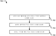
[0011] FIG. 7 illustrates a flow chart illustrating a communication method using a quasi-Yagi-type antenna.
[0012] 아래에 명시된 상세한 설명은 본 개시의 예시적인 설계들의 설명으로서 의도되고 본 개시가 실시될 수 있는 유일한 설계를 나타내도록 의도되진 않는다. "예시적인" 이란 용어는 "예, 인스턴스 또는 예시로서 작용하는 것"을 의미하도록 본 명세서에서 이용된다. "예시적인" 것으로서 본 명세서에서 설명되는 임의의 설계는 반드시 다른 설계들보다 선호되거나 유리한 것으로서 해석될 필요는 없다. 상세한 설명은 본 개시의 예시적인 설계들의 완전한 이해를 제공하기 위해 특정한 세부사항들을 포함한다. 여기서 설명되는 예시적인 설계들은 이들 특정한 세부사항들 없이 실시될 수 있다는 것이 당업자들에게 명백하게 될 것이다. 일부 인스턴스들에서, 잘-알려진 구조들 및 디바이스들은 여기에 제시된 예시적인 설계들의 신규성을 모호하게 하는 것을 방지하기 위해 블록도 형태로 도시된다.[0012] The following detailed description is intended as a description of exemplary designs of the present disclosure and is not intended to represent the only designations in which the present disclosure may be practiced. The word "exemplary" is used herein to mean "serving as an example, instance, or illustration. &Quot; Any design described herein as "exemplary " is not necessarily to be construed as preferred or advantageous over other designs. The detailed description includes specific details in order to provide a thorough understanding of the exemplary designs of the present disclosure. It will be apparent to those skilled in the art that the exemplary designs described herein may be practiced without these specific details. In some instances, well-known structures and devices are shown in block diagram form in order to avoid obscuring the novelty of the exemplary designs presented herein.
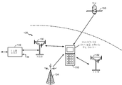
[0013] 도 1은 무선 통신 시스템(120)과 통신하는 무선 디바이스(110)를 도시한다. 무선 통신 시스템(120)은 각각 LTE(Long Term Evolution) 시스템, CDMA(Code Division Multiple Access) 시스템, GSM(Global System for Mobile Communications) 시스템, WLAN(wireless local area network) 시스템, 하나 또는 그 초과의 IEEE(Institute of Electrical and Electronics Engineers) 프로토콜들 또는 표준들(예를 들어, IEEE 802.11ad)에 따라 동작하는 무선 시스템, 60GHz 무선 시스템, 밀리미터파(mm-wave) 무선 시스템, 또는 몇몇 다른 무선 시스템일 수 있다. CDMA 시스템은 WCDMA(Wideband CDMA), CDMA 1X, EVDO(Evolution-Data Optimized), TD-SCDMA(Time Division Synchronous CDMA), 또는 몇몇 다른 버전의 CDMA를 구현할 수 있다. 단순함을 위해, 도 1은 2개의 기지국들(130 및 132) 및 하나의 시스템 제어기(140)를 포함하는 무선 통신 시스템(120)을 도시한다. 일반적으로, 각각의 무선 시스템은 임의의 수의 기지국들 및 임의의 세트의 네트워크 엔티티들을 포함할 수 있다.[0013] FIG. 1 illustrates a
[0014] 무선 디바이스(110)는 사용자 장비(UE), 모바일 스테이션, 단말, 액세스 단말, 가입자 유닛, 스테이션 등으로서 또한 지칭될 수 있다. 무선 디바이스(110)는 셀룰러 전화, 스마트폰, 태블릿, 무선 모뎀, 개인용 디지털 보조기기(PDA), 핸드헬드 디바이스, 랩톱 컴퓨터, 스마트북, 넷북, 코드리스 전화, 무선 로컬 루프(WLL) 스테이션, 블루투스 디바이스 등일 수 있다. 무선 디바이스(110)는 무선 통신 시스템(120)과 통신할 수 있다. 무선 디바이스(110)는 브로드캐스트 스테이션들(예를 들어, 브로드캐스트 스테이션(134))로부터의 신호들, 하나 또는 그 초과의 GNSS(global navigation satellite systems)에서 위성들(예를 들어, 위성(150))로부터의 신호들 등을 또한 수신할 수 있을 수 있다. 무선 디바이스(110)는 LTE, WCDMA, CDMA 1X, EVDO, TD-SCDMA, GSM, IEEE 802.11ad, 무선 기가비트, 60GHz 주파수 대역 통신, mm-wave 통신 등과 같은 무선 통신을 위한 하나 또는 그 초과의 라디오 기술들을 지원할 수 있다.[0014] The
[0015] 또한, 예시적인 실시예에서, 본원에서 추가로 설명되는 바와 같이, 무선 디바이스(110)는 (예를 들어, 하나 또는 그 초과의 안테나 어레이들의 부분으로서) 하나 또는 그 초과의 쿼시-야기-타입 안테나들을 포함할 수 있다. 특정한 예에서, 쿼시-야기-타입 안테나는 2개의 접지 플레인들 간에 발룬(balun)을 갖고 인쇄 회로 보드(PC)의 에지로부터 연장하는 다이폴을 갖는 안테나일 수 있다. 비아들은 반사기로서 기능하는 에지의 또는 그 근처의 비아 "벽"을 생성하도록 접지 플레인들 간에 커플링될 수 있다. 예시적인 쿼시-야기-타입 안테나(들)가 도 3 내지 도 5를 참조하여 추가로 설명된다.[0015] Also, in an exemplary embodiment, as further described herein,
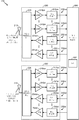
[0016] 도 2는 무선 디바이스(110)의 컴포넌트들의 예시적인 설계의 블록도를 도시한다. 예시적인 설계에서, 무선 디바이스(110)는 주 안테나 어레이(210)에 커플링되는 트랜시버(220), 보조 안테나 어레이(212)에 커플링되는 트랜시버(222) 및 데이터 프로세서/제어기(280)를 포함한다. 트랜시버(220)는 다수의 주파수 대역들, 다수의 라디오 기술들, 캐리어 어그리게이션 등을 지원하기 위해 다수(K)의 수신기들(230pa 내지 230pk) 및 다수(K)의 송신기들(250pa 내지 250pk)을 포함한다. 트랜시버(222)는 다수의 주파수 대역들, 다수의 라디오 기술들, 캐리어 어그리게이션, 수신 다이버시티, 다수의 송신 안테나들로부터 다수의 수신 안테나들로의 다중-입력 다중-출력(MIMO) 송신 등을 지원하기 위해 다수(L)의 수신기들(230sa 내지 230sl) 및 다수(L)의 송신기들(250sa to 250sl)을 포함한다.[0016] FIG. 2 shows a block diagram of an exemplary design of components of a
[0017] 주 안테나 어레이(210) 및/또는 보조 안테나 어레이(212)는 도 3 내지 도 5를 참조하여 추가로 설명되는 바와 같은 하나 또는 그 초과의 쿼시-야기-타입 안테나들을 포함할 수 있다. 또한, 주 안테나 어레이(210) 및/또는 보조 안테나 어레이(212)는 도 4를 참조하여 추가로 설명되는 바와 같이, 패치 안테나들과 같은 하나 또는 그 초과의 다른 안테나 타입들을 포함할 수 있다.The
[0018] 도 2에서 도시된 예시적인 설계에서, 각각의 수신기(230)는 LNA(240) 및 수신 회로들(242)을 포함한다. 데이터 수신을 위해, 주 안테나 어레이(210)는 기지국들 및/또는 다른 송신기 스테이션들로부터 신호들을 수신하고, 수신된 RF 신호를 제공하며, 이는 안테나 인터페이스 회로(224)를 통해 라우팅되고, 입력 RF 신호로서 선택된 수신기에 제공된다. 안테나 인터페이스 회로(224)는 스위치들, 듀플렉서들, 송신 필터들, 수신 필터들, 매칭 회로들 등을 포함할 수 있다. 아래의 설명은, 수신기(230pa)가 선택된 수신기라고 가정한다. 수신기(230pa) 내에서, LNA(240pa)는 입력 RF 신호를 증폭하고 출력 RF 신호를 제공한다. 수신 회로들(242pa)은 RF로부터 기저대역으로 출력 RF 신호를 하향변환하고, 하향변환된 신호를 증폭 및 필터링하고, 아날로그 입력 신호를 데이터 프로세서/제어기(280)에 제공한다. 수신 회로들(242pa)은 믹서들, 필터들, 증폭기들, 매칭 회로들, 오실레이터, 로컬 오실레이터(LO) 생성기, 위상 동기 루프(PLL) 등을 포함할 수 있다. 트랜시버들(220 및 222)의 각각의 잔여 수신기(230)는 수신기(230pa)와 유사한 방식으로 동작할 수 있다.[0018] In the exemplary design shown in FIG. 2, each receiver 230 includes an LNA 240 and receive circuits 242. For data reception, the
[0019] 도 2에서 도시된 예시적인 설계에서, 각각의 송신기(250)는 송신 회로들(252) 및 전력 증폭기(PA)(254)를 포함한다. 데이터 송신을 위해, 데이터 프로세서/제어기(280)는 송신될 데이터를 프로세싱(예를 들어, 인코딩 및 변조)하고 아날로그 출력 신호를 선택된 송신기에 제공한다. 아래의 설명은 송신기(250pa)가 선택된 송신기라고 가정한다. 송신기(250pa) 내에서, 송신 회로들(252pa)은 아날로그 출력 신호를 증폭 및 필터링하고 기저대역으로부터 RF로 상향변환하고, 변조된 RF 신호를 제공한다. 송신 회로들(252pa)은 증폭기들, 필터들, 믹서들, 매칭 회로들, 오실레이터, LO 생성기, PLL 등을 포함할 수 있다. PA(254pa)는 변조된 RF 신호를 수신 및 증폭하고 적절한 출력 전력 레벨을 갖는 송신 RF 신호를 제공한다. 송신 RF 신호는 안테나 인터페이스 회로(224)를 통해 라우팅되고 주 안테나 어레이(210)를 통해 송신된다. 트랜시버들(220 및 222) 내의 각각의 잔여 송신기(250)는 송신기(250pa)와 유사한 방식으로 동작할 수 있다.[0019] In the exemplary design shown in FIG. 2, each transmitter 250 includes transmit circuits 252 and a power amplifier (PA) 254. For data transmission, the data processor /
[0020] 도 2는 수신기(230) 및 송신기(250)의 예시적인 설계를 도시한다. 수신기 및 송신기는 또한 필터들, 매칭 회로들 등과 같이 도 2에서 도시되지 않은 다른 회로들을 포함할 수 있다. 트랜시버들(220 및 222) 중 일부 또는 모두 다는 하나 또는 그 초과의 아날로그 집적 회로들(IC들), RF IC들(RFIC들), 믹싱된-신호 IC들 등 상에서 구현될 수 있다. 예를 들어, LNA들(240) 및 수신 회로들(242)은 RFIC 등일 수 있는 하나의 모듈들 상에서 구현될 수 있다. 트랜시버들(220 및 222)의 회로들은 다른 방식들로 또한 구현될 수 있다. RFIC는 도 4에서 예시된 바와 같은 패치 안테나들과 같은 안테나들을 또한 포함하는 SiP(system in package)에 포함될 수 있다.[0020] FIG. 2 illustrates an exemplary design of a receiver 230 and a transmitter 250. The receiver and transmitter may also include other circuits not shown in Fig. 2, such as filters, matching circuits, and the like. Some or all of the
[0021] 데이터 프로세서/제어기(280)는 무선 디바이스(110)에 대한 다양한 기능들을 수행할 수 있다. 예를 들어, 데이터 프로세서/제어기(280)는 수신기(230)를 통해 수신된 데이터 및 송신기(250)를 통해 송신될 데이터에 대한 프로세싱을 수행할 수 있다. 데이터 프로세서/제어기(280)는 트랜시버들(220 및 222) 내의 다양한 회로들의 동작을 제어할 수 있다. 메모리(282)는 데이터 프로세서/제어기(280)에 대한 프로그램 코드들 및 데이터를 저장할 수 있다. 데이터 프로세서/제어기(280)는 하나 또는 그 초과의 주문형 집적 회로들(ASIC들) 및/또는 다른 IC들 상에 구현될 수 있다.[0021] Data processor /
[0022] 무선 디바이스(110)는 다수의 주파수 대역 그룹들, 다수의 라디오 기술들 및/또는 다수의 안테나들을 지원할 수 있다. 무선 디바이스(110)는 다수의 주파수 대역 그룹들, 다수의 라디오 기술들 및/또는 다수의 안테나들을 통한 수신을 지원하기 위해 다수의 LNA들을 포함할 수 있다.[0022] The
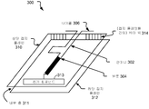
[0023] 도 3은 2개의 접지 플레인들 간의 발룬(304)을 포함하고 쿼시-야기-타입 안테나로서 구성된 안테나(302)를 포함하는 안테나 구조(300)를 예시한다. 안테나(302)는 무선 디바이스(110)의 안테나 어레이들(210-212)과 같은 안테나 어레이의 하나 또는 다수의 안테나들일 수 있다. 본원에서 이용되는 바와 같이, "안테나 구조"는 발룬 및 안테나를 포함하는 구조로서 정의되고, "안테나"는 전자기파들이 전송 또는 수신될 수 있는 임의의 전도성 엘리먼트로서 정의되고, "발룬"은 밸런싱된 신호(예를 들어, 차동 신호) 및 언밸런싱 신호(예를 들어, 싱글-엔드 신호) 사이에서 변환하는 임의의 디바이스로서 정의된다. [0023] FIG. 3 illustrates an
[0024] 안테나(302)는 다이폴 부분(306) 및 다이폴 부분(306)을 발룬(304)에 커플링하는 와이어 부분을 포함한다. 발룬(304)은 예컨대, 인입하는 신호를 수신하고 다이폴 부분(306)에 제공되는 위상 조정 신호를 생성함으로써 수신된 언밸런싱 신호를 밸런싱된 신호로 변환하도록 구성된다. 예를 들어, 발룬(304)은 인입하는 신호를 수신하기 위한 입력을 갖는 것으로서 예시되며, 2개의 신호 경로들의 출력 신호들 간에 위상 지연을 도입하기 위해 상이한 길이들의 2개의 신호 경로들을 포함한다. 출력 신호들은 다이폴 부분(306)에 제공된다. 다이폴 부분(306)은 2개의 다이폴 "암(arm)"들을 포함한다. 각각의 다이폴 암은 발룬(304)의 각각의 신호 경로에 커플링된다. [0024] The antenna 302 includes a dipole portion 306 and a wire portion that couples the dipole portion 306 to the balun 304. The balun 304 is configured to convert the received unbalanced signal into a balanced signal, for example, by receiving an incoming signal and generating a phase adjustment signal provided to the dipole portion 306. [ For example, the balun 304 is illustrated as having an input for receiving an incoming signal and includes two signal paths of different lengths for introducing a phase delay between the output signals of the two signal paths. Output signals are provided to the dipole portion 306. The dipole portion 306 includes two dipole "arms ". Each dipole arm is coupled to a respective signal path of the balun 304.
[0025] 안테나(302)의 적어도 일부(예를 들어, 다이폴 부분(306) 및 발룬(304) 간의 와이어 부분의 일부)는 제 1 접지 플레인(310)(예를 들어, 상단 접지 플레인) 및 제 2 접지 플레인(312)(예를 들어, 하단 접지 플레인) 간에 있는 모듈의 내부 층(311)에 배치된다. 접지 플레인들 간의 층은 대안적으로 인터층으로서 지칭될 수 있다. 접지 플레인들(310, 312)은 PC 보드와 같은 기판의 표면들 또는 내부 층들에 로케이팅될 수 있다. 복수의 비아들은 2개의 접지 플레인들(310, 312)을 서로 커플링하고 다이폴 부분(306)의 반사기로서 기능하는 전도성 "비아 벽"(314)을 형성할 수 있다.At least a portion of the antenna 302 (e.g., a portion of the wire portion between the dipole portion 306 and the balun 304) is coupled to the first ground plane 310 (e.g., top ground plane) 2 < / RTI > ground plane 312 (e. G., The bottom ground plane). The layer between the ground planes may alternatively be referred to as an interlayer. The ground planes 310 and 312 may be located on surfaces or inner layers of a substrate such as a PC board. The plurality of vias may form a conductive "via wall" 314 that couples the two
[0026] 안테나(302)에는 2개의 접지 플레인들(310, 312) 간의 내부 층(311)에 배치되는 스트립라인 및 발룬 피드가 제공될 수 있다. 예를 들어, 발룬(304)은 포토리소그래피 및 금속 증착 프로세스를 이용함으로써 내부 층(311)의 유전체 물질에 형성될 수 있다. 예시를 위해, 유전체 물질이 하단 접지 플레인(312) 상에 증착될 수 있고, 포토리소그래피 및 금속 증착 프로세스는 하단 접지 플레인(312) 위에 발룬(304)의 도전성 와이어 패턴을 형성하는데 이용될 수 있고, 상단 접지 플레인(310)은 발룬(304) 위에 형성될 수 있다. 안테나 피드, 도파관, 송신 라인, 커넥터 등과 같은 하나 또는 그 초과의 전기 컴포넌트들(313)이 또한 발룬(304)에 커플링될 수 있다. 예를 들어, 안테나 피드는 튜너 유닛 및/또는 임피던스 매칭 컴포넌트를 포함할 수 있고, 안테나로의 신호들의 송신 또는 안테나로부터의 그의 수신 동안 수신된 신호를 조정하도록 동작할 수 있다. 공면 도파관(coplanar waveguide)과 같은 도파관이 저-손실 라디오 파 전파 매체를 제공함으로써 동작할 수 있다. 마이크로스트립 또는 스트립라인과 같은 송신 라인은 안테나로 또는 이로부터의 전파 경로를 제공함으로써 동작할 수 있다. 커넥터는 증폭기(예를 들어, 도 2의 LNA(240pa) 또는 PA(254pa))와 같은 다른 컴포넌트와 발룬 간의 신호 전파를 인에이블하도록 연결을 제공함으로써 동작할 수 있다.The antenna 302 may be provided with a strip line and a balun feed disposed in the inner layer 311 between the two
[0027] 도 3에서 예시된 바와 같은 쿼시-야기-타입 안테나는 2개의 접지 플레인들에도 불구하고 효율적으로 방사한다. 예를 들어, 쿼시-야기-타입 안테나는 RF 모듈에 포함될 수 있고 비아 벽(314)의 비아들은 특정한 방사선을 반사하도록 하는 위치에 배치될 수 있지만, RF 모듈 외부로의 신호 방사를 허용하는 개구를 또한 갖는다. 접지 플레인들(310, 312) 각각은 접지 플레인(310 또는 312)의 반대 측들 상의 안테나들 간에 간섭을 감쇄 또는 제거하기 위해 전자기 차폐를 제공할 수 있다. (도시된 바와 같은) 모듈의 내부 층들에 포함되는 안테나를 설계하는 것은 영역 당 안테나 밀도를 더 높게 할 수 있다. 예를 들어, 도 4 내지 도 5에 관하여 추가로 설명되는 바와 같이, 안테나 밀도는, 스택들의 안테나들 간에 간섭을 감소시키기 위해 접지 플레인들에 의해 분리되는 층들로 안태나들을 "스택"시킴으로써 증가될 수 있다.[0027] A quasi-Yagi-type antenna as illustrated in FIG. 3 emits efficiently despite two ground planes. For example, a quasi-yagi-type antenna may be included in the RF module and the vias in the via wall 314 may be placed in a position to reflect a particular radiation, but an opening that allows signal radiation out of the RF module . Each of the ground planes 310 and 312 may provide electromagnetic shielding to attenuate or eliminate interference between the antennas on opposite sides of the
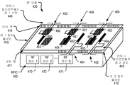
[0028] 도 4는 다수의 쿼시-야기-타입 안테나들(402, 404, 406, 452, 및 454)을 포함하는 예시적인 RF 모듈(430)을 예시한다. 쿼시-야기-타입 안테나들 각각은 제 1 접지 플레인(410)과 제 2 접지 플레인(412) 간의 RF 모듈(430)의 내부 층(411) 내에 있다. 제 1 접지 플레인(410) 및 제 2 접지 플레인(412)은 RF 모듈(430)의 상단 및 하단 표면들 상에서 쿼시-야기-타입 안테나들 및 컴포넌트들 간의 간섭을 감소시키도록 방사를 차단할 수 있다. 예를 들어, 다른 안테나들(460-465), 예컨대 패치 안테나들은 접지 플레인의 외부 층 상에(예를 들어, 제 1 접지 플레인(410)이 쿼시-야기-타입 안테나들의 발룬들(480-484)과 패치 안테나들 간에 있도록 제 1 접지 플레인(410) 상에) 로케이팅될 수 있다.[0028] FIG. 4 illustrates an
[0029] 다수의 쿼시-야기-타입 안테나 엘리먼트들은 (예를 들어, RF 모듈(430)의 에지 표면으로부터 돌출하는) 제 1 및 제 2 접지 플레인들(410, 412) 외부에 배치되는 다이폴 부분들을 가지며, 다이폴 부분들은 접지 플레인들(410, 412) 간에 배치되는 발룬들에 커플링된다. 비아 벽(414)은 다이폴들 중 하나 또는 그 초과에 대한 반사기로서 기능하도록 접지 플레인들(410, 412) 간에 포지셔닝될 수 있다.A plurality of quasi-yagi-type antenna elements may include dipole portions disposed outside first and second ground planes 410, 412 (e.g., projecting from the edge surface of RF module 430) And the dipole portions are coupled to the baluns disposed between the ground planes 410 and 412. The via
[0030] 쿼시-야기-타입 안테나들의 다수의 세트들은 RF 모듈(430)의 상이한 에지들 부근에 형성될 수 있다. 예를 들어, 도시된 바와 같이, 안테나 엘리먼트들의 제 1 세트(440)는 안테나들(402, 404 및 406)을 포함할 수 있고, 안테나 엘리먼트들의 제 2 세트(442)는 안테나들(452 및 454)을 포함할 수 있으며, 이들 각각은 각각의 발룬(480-484)에 커플링될 수 있다. RF 모듈(430)의 2개의 에지들을 따라 쿼시-야기-타입 안테나들의 2개의 세트들을 갖는 RF 모듈(430)이 예시되지만, 다른 구현들에서, 쿼시-야기-타입 안테나들들의 2개 초과의 세트들이 포함될 수 있다. 예를 들어, 쿼시-야기-타입 안테나들의 4개의 세트들이 포함될 수 있고, RF 모듈(430)의 4개의 에지들이 쿼시-야기-타입 안테나들을 포함하도록 각각의 세트는 RF 모듈(430)의 각각의 에지 부근에 있을 수 있다.[0030] Multiple sets of quasi-Yagi-type antennas may be formed near different edges of the
[0031] RF 모듈(430)이 쿼시-야기-타입 안테나들의 단일 층을 갖는 것으로서 예시되지만, 접지 플레인에 의해 분리되는 쿼시-야기-타입 안테나들의 부가적인 층들이 도 5에 관하여 추가로 상세히 설명되는 바와 같이 RF 모듈에 포함될 수 있다. 일부 실시예들에서, 안테나들의 2개 초과의 층들이 RF 모듈에 포함될 수 있다.[0031] Although the
[0032] RF 모듈(430)은 다수의 RF 체인들(470-474)(예를 들어, 믹서, 증폭기들 등)을 포함하는 라디오 주파수 집적 회로(RFIC)(450)에 커플링될 수 있다. 예를 들어, "N"개의 RF 체인들(470-474)이 RFIC(450)에 포함될 수 있으며, 여기서 N은 1보다 큰 임의의 양의 정수이다. RFIC(450) 내의 적어도 하나의 RF 체인(470-474)은 복수의 안테나 엘리먼트들(예를 들어, 쿼시-야기-타입 안테나들(402, 404, 406, 452, 및 454)) 중 제 1 안테나 엘리먼트에 커플링될 수 있다. 제 2 접지 플레인(412)은 RF 모듈(430)의 하단 접지 플레인일 수 있다. 제 2 접지 플레인(412)은 RFIC(450)와 발룬들(480-484) 사이에 배치될 수 있고, RFIC(450)의 컴포넌트들과 RF 모듈(430)의 안테나들 간의 간섭을 감소시킬 수 있다. RFIC(450)가 RF 모듈(430)(예를 들어, PC 보드) 아래에 예시되고 RF 모듈(430)보다 더 뚜꺼운 것으로서 예시되지만, 다른 실시예들에서, RFIC(450)는 RF 모듈(430)에 대하여 다른 포지션(예를 들어, 인접, 위 등)을 가질 수 있고 RF 모듈(430)에 대하여 상이한 두께(예를 들어, RF 모듈(430)과 실질적으로 동일한 두께 또는 RF 모듈(430)보다 더 얇은 두께)를 가질 수 있다. RF 체인들(470-474)은 RF 모듈(430)의 개별 안테나 엘리먼트들에 커플링될 수 있다.The
[0033] (쿼시-야기-타입 안테나들(402-406 및 452-454) 또는 안테나들(460-465)과 같은 다른 타입들의 안테나들을 포함하는) RF 모듈(430)의 안테나들은 개별적으로 또는 하나 또는 그 초과의 어레이들의 부분으로서 동작될 수 있다. 안테나의 그룹이 안테나 어레이로서 동작될 때, 어레이의 각각의 안테나는 빔-포밍을 위해 RF 모듈(430) 내의 각각의 위상 시프터에 커플링될 수 있다. 예를 들어, RF 모듈(430)은 다수의 위상 시프터들을 포함할 수 있다. 안테나 어레이의 각각의 안테나는 각각의 위상 시프터에 커플링될 수 있다. 예를 들어, 패치 안테나들(460-465) 각각은 위상 시프터에 커플링될 수 있고, 쿼시-야기-타입 안테나들(402, 404, 406, 452, 및 454) 각각은 위상 시프터에 커플링될 수 있다. 위상 시프터들 각각은 안테나 어레이의 안테나에 의해 송신되는 신호를 수신하도록 그리고 위상 오프셋을 신호에 도입하도록 구성될 수 있다. 위상 시프터에 의해 생성된 각각의 위상-시프트된 신호는 안테나에 의한 송신을 위해 위상 시프터에 커플링되는 안테나에 제공된다. 어레이의 다수의 안테나들로부터의 결과적인 위상-시프트된 송신들은 송신된 신호에서 건설적이고 파괴적인 간섭을 유발하여 지향성 신호 송신(예를 들어, 빔-포밍)을 발생시킬 수 있다.The antennas of the RF module 430 (including the quasi-Yagi-type antennas 402-406 and 452-454 or other types of antennas such as the antennas 460-465) Or as part of arrays beyond that. When a group of antennas is operated as an antenna array, each antenna of the array may be coupled to a respective phase shifter in the
[0034] 쿼시-야기-타입 안테나들 및 다른 안테나들(460-465)(예를 들어, 패치 안테나들)과 같은 다수의 타입들의 안테나들이 RF 모듈(430)에 포함될 수 있기 때문에, 단일 타입의 안테나를 이용하는 것에 비해 더 넓은 신호 커버리지가 제공될 수 있다. 예를 들어, 안테나들의 하나 또는 그 초과의 어레이들은 상이한 지향성 특성을 제공하고 상이한 방사 패턴들을 가질 수 있는 다수의 타입들의 안테나들을 포함할 수 있다. 안테나 어레이 내의 안테나 포지션들의 다이버시티, 안테나 배향들 및 안테나 타입들은 안테나 어레이에 대해 개선된 전체 커버리지를 제공할 수 있다.[0034] Because multiple types of antennas, such as quasi-Yagi-type antennas and other antennas 460-465 (e.g., patch antennas) may be included in the
[0035] RF 모듈(430)이 제 1 접지 플레인(410) 상에 안테나들(460-465)을 갖는 것으로서 예시되지만, 다른 실시예들에서, 하나 또는 그 초과의 표면 장착 기술(SMT) 컴포넌트들과 같은 다른 디바이스들이 제 1 접지 플레인(410) 상에 장착될 수 있다. 예를 들어, SMT 컴포넌트는 하나 또는 그 초과의 인덕터들, 하나 또는 그 초과의 커패시터들, 및/또는 RF 모듈(430)의 표면에 장착된 집적 회로(IC)를 포함할 수 있다. RF 모듈(430)의 표면 상에 SMT 컴포넌트를 장착하는 것은 감소된 비용으로 보다 간결한 PCB를 가능케 할 수 있다.Although
[0036] 3개의 쿼시-야기-타입 안테나들(402-406)이 RF 모듈(430)의 하나의 에지를 따라 도시되고, 2개의 쿼시-야기-타입 안테나들(402-406)은 RF 모듈(430)의 다른 에지를 따라 도시되고, 6개의 다른 안테나들(460-465)이 도 4에서 제 1 접지 플레인(410) 상에서 도시되지만, 공간 가용성 및 설계 제약들에 의존하여, 임의의 수의 안테나들이 RF 모듈(430)의 임의의 표면 및/또는 에지들 중 임의의 것 상에 배치될 수 있다. 일부 구현들에서, RF 체인들(470-474)의 수가 RF 모듈(430)의 안테나들의 수와 동일하고, 각각의 RF 체인이 각각의 안테나에 이용하도록 전용되지만, 다른 구현들에서, RF 체인들의 수는 안테나들의 수와 상이하며, 스위칭 회로(예를 들어, 고속 크로스바)가 RF 체인들을 안테나들에 선택적으로 커플링하거나 디커플링하는데 이용될 수 있다. Three quasi-Yagi-type antennas 402-406 are shown along one edge of the
[0037] 접지 플레인들(410, 412) 간에 다수의 쿼시-야기-타입 안테나들을 포함함으로써, 부가적인 안테나들(460-465)은 또한 강화된 안테나 밀도를 위해 RF 모듈(430)의 부분으로서 포함될 수 있다. 안테나 커버리지 및 안테나 어레이 애플리케이션들, 예컨대, 빔-포밍은 단일 RF 모듈(430)에서 안테나 배향들의 다이버시티, 안테나 포지션들, 및 안테나 타입들을 이용함으로써 강화될 수 있다. 따라서, 도 4는, 강화된 안테나 밀도를 제공하고 강화된 안테나 커버리지 및 강화된 안테나 어레이 애플리케이션들을 제공할 수 있는 RF 모듈을 예시한다.By including a plurality of quasi-Yagi-type antennas between the ground planes 410 and 412, additional antennas 460-465 may also be included as part of the
[0038] 도 5는 다수의 접지 플레인들 및 접지 플레인들 간의 안테나들을 포함하는 모듈(500)의 예시적인 실시예를 예시한다. 제 1 접지 플레인(510) 및 제 2 접지 플레인(512)은 각각 모듈(500)의 상단 및 하단 접지 플레인들일 수 있다. 제 3 접지 플레인(514)은 상단(510) 및 하단(512) 접지 플레인들 간에 포지셔닝된다.[0038] FIG. 5 illustrates an exemplary embodiment of a
[0039] 제 1 복수의 안테나 엘리먼트들(540)은 제 1 복수의 발룬들(542)에 커플링된다. 제 1 복수의 발룬들(542)의 각각의 발룬은 제 1 접지 플레인(510)과 제 3 접지 플레인(514) 간의 제 1 내부 층(511)에 배치된다. 제 1 복수의 안테나 엘리먼트들(540) 중 안테나 엘리먼트들의 제 1 세트는 제 1 내부 층(511)의 제 1 에지(591) 부근에 로케이팅될 수 있다. 예를 들어, 안테나 엘리먼트들의 제 1 세트의 다이폴들은 제 1 내부 층(511)의 제 1 에지(591)로부터 바깥쪽으로 연장하고 제 1 에지(591) 근처에 또한 포지셔닝되는 각각의 발룬들에 커플링된다. 제 1 복수의 안테나 엘리먼트들(540) 중 안테나 엘리먼트(도시되지 않음)의 제 2 세트는 제 1 내부 층(511)의 제 2 에지(592) 부근에 로케이팅될 수 있다. 예를 들어, 안테나 엘리먼트들의 제 1 세트 및 제 2 세트는 도 4에서 예시된 안테나 엘리먼트들의 제 1 세트(440) 및 제 2 세트(442)에 대응할 수 있다. 제 2 복수의 안테나 엘리먼트들(544)은 제 2 복수의 발룬들(546)에 커플링된다. 제 2 복수의 발룬들(546)은 제 3 접지 플레인(514)과 제 2 접지 플레인(512) 간의 제 2 내부 층(513) 내에 배치된다.[0039] A first plurality of antenna elements 540 are coupled to the first plurality of baluns 542. Each balun of the first plurality of baluns 542 is disposed in the first inner layer 511 between the
[0040] 도 5가 단일 접지 플레인에 의해 분리되는 쿼시-야기-타입 안테나들의 2개의 층들을 예시하지만, 다른 실시예들에서, 안테나들의 2개 초과의 층들이 모듈 내에서 다수의 접지 플레인들에 의해 분리될 수 있다. 대안적으로 또는 부가적으로, 패치 안테나들과 같은 하나 또는 그 초과의 다른 타입들의 안테나들이 도 4에서 도시된 것과 유사한 방식으로, 제 1 접지 플레인(510)의 상위 표면 상에 포함될 수 있다. 모듈(500)은 도 4의 RFIC(450)와 같은 RFIC에 연결될 수 있다. 예를 들어, 모듈(500)은 접지 플레인들(510, 512, 514)을 통해 RF 모듈(500)의 상이한 층들의 안테나들로 신호 라우팅을 가능하게 하도록 비아들 또는 다른 전도성 구조들을 포함할 수 있다. 접지 플레인들 간의 내부 층들에 안테나들을 포지셔닝함으로써, 몇 개의 안테나들은, 안테나의 단일 층을 이용하는 것에 비해 증가된 안테나 밀도를 제공하도록 모듈(500) 내에서 스택될 수 있다.[0040] Although FIG. 5 illustrates two layers of quasi-Yagi-type antennas separated by a single ground plane, in other embodiments, two or more layers of antennas are disposed in a plurality of ground planes Lt; / RTI > Alternatively or additionally, one or more other types of antennas, such as patch antennas, may be included on the top surface of the
[0041] 도 6은 도 3의 안테나 구조(300)와 같은 쿼시-야기-타입 안테나를 설계하기 위한 예시적이고 비-제한적인 방법을 예시한다. 전체 다이폴 길이(예를 들어, 도 3의 다이폴 부분(306)의 팁(tip) 간 거리)는 602에서, λ/2로 나누어지는 파장(λ)과 동일할 수 있는 값으로 세팅된다. 예를 들어, 파장은 쿼시-야기-타입 안테나에 의해 송신될 신호의 파장(예를 들어, 60GHz 신호에 대해 대략 5 밀리미터(mm)의 파장)에 대응할 수 있다. 전체 다이폴 길이에 기초하여, 다이폴 암들 간의 최소 간격이 정의되고, 다이폴 암 길이들이 계산된다. 다이폴로부터 접지된 비아 벽까지의 거리(예를 들어, 도 3의 비아 벽(314)과 다이폴 부분(306)의 암들 간의 거리)는 604에서 λ/4로 세팅된다. 다이폴로부터 유전체 에지까지의 거리는 606에서 λ/4로 세팅된다. 비아 벽의 비아들 간의 분리 거리가 608에서 세팅된다. 예를 들어, 분리 거리는 제조 기술에 의해 정의되는 분리를 통해 허용되는 최소치로 세팅될 수 있다.[0041] FIG. 6 illustrates an exemplary, non-limiting method for designing a quasi-Yagi-type antenna such as the
[0042] 접지 에지로부터 발룬 거리(예를 들어, 발룬(304)과 하단 접지 플레인(312)의 상위 표면 간의 분리)는, 610에서 다이폴에 대해 2개의 신호 경로들을 따른 신호 전파의 결과적인 차동 모드의 품질이 차동 신호 품질 임계치를 충족하도록 정의된다. 예를 들어, 발룬(304)은 다이폴 부분(306)의 두 개의 암들에서 신호들("V1" 및 "V2") 간에 실질적으로 180도의 위상 시프트를 생성하도록 설계될 수 있으며, 여기서 V1 및 V2는 실질적으로 동일한 진폭을 갖는다. 차동 신호의 품질은 공통 모드(V1+V2) 대 차동 모드(V1-V2)/2의 비에 의해 정의될 수 있다. 이상적인 차동 신호는 0 공통 모드(즉, V1=-V2)를 갖는다. 발룬과 접지 플레인 간의 분리는 차동 신호의 품질이 차동 신호 품질 임계치와 매칭하거나 초과하도록 세팅될 수 있다. 결정된 다이폴 암 길이들, 다이폴 암들 간의 간격, 비아 벽과 다이폴 암들 간의 거리 및 접지 플레인과 발룬 간의 분리를 갖는 결과적인 안테나는 612에서 시뮬레이트되고 매칭의 검사가 수행된다. 충분한 대역폭이 결과적인 안테나의 시뮬레이션에 기초하여 달성되지 않는 경우, 위에서 설명된 하나 또는 그 초과의 파라미터들이 조정되는데, 예컨대 더 넓은 매칭을 위해 발룬과 접지 플레인 간의 분리를 증가시키고, 더 낮은 또는 더 높은 중앙 주파수에 도달하도록 다이폴 길이를 증가 또는 감소시키고, 및/또는 다른 파라미터들을 조정하고, 그 후 이어지는 프로세싱을 위해 602로 리턴한다.The separation of the balun distance from the ground edge (e.g., separation between the balun 304 and the upper surface of the lower ground plane 312) causes the resulting differential mode of signal propagation along the two signal paths to the dipole at 610 Is defined to meet the differential signal quality threshold. For example, the balun 304 may be designed to produce a phase shift of substantially 180 degrees between the signals ("V1" and "V2") at the two arms of the dipole portion 306, where V1 and V2 And have substantially the same amplitude. The quality of the differential signal can be defined by the ratio of the common mode (V1 + V2) to the differential mode (V1-V2) / 2. The ideal differential signal has a zero common mode (i.e., V1 = -V2). The separation between the balun and the ground plane may be set such that the quality of the differential signal matches or exceeds the differential signal quality threshold. The resulting antenna with the determined dipole arm lengths, the spacing between the dipole arms, the distance between the via wall and the dipole arms, and the separation between the ground plane and the balun is simulated at 612 and a match check is performed. If sufficient bandwidth is not achieved based on the simulation of the resulting antenna, one or more of the parameters described above may be adjusted, for example to increase the separation between the balun and the ground plane for a wider match, Increase or decrease the dipole length to reach the center frequency, and / or adjust other parameters, and then return to 602 for subsequent processing.
[0043] 충분한 대역폭이 시뮬레이션 기초하여 달성되면, 안테나 패턴(즉, 안테나로부터 지향성 변위의 함수로서 안테나로부터 방사의 신호 세기)이 614에서 시뮬레이트된다. 접지 크기, 접지까지의 거리, 유전체 에지까지의 거리 및/또는 비아 거리의 파라미터들은 616에서 안테나 패턴을 조정 또는 "튜닝"하도록 변경될 수 있다. 다른 실시예들에서, 하나 또는 그 초과의 디렉터들(예를 들어, 야기-타입 공진기 엘리먼트들)은 증가된 안테나 크기의 댓가로 더 높은 이득을 위해 안테나 방사 패턴을 변형하도록 안테나에 부가될 수 있다. 안테나 패턴 시뮬레이션은 618에서 매칭이 영향을 받지 않는다는 것을 검증하도록 (616의 조정들 이후) 반복된다. 매칭이 영향을 받은 경우, 패턴 및 매칭은 공동-튜닝될 수 있다. 예를 들어, 다이폴 암 길이 및 접지 플레인으로부터의 거리와 같은 일부 안테나 파라미터들은 안테나 패턴 및 매칭 둘 다에 영향을 준다. 다른 안테나 파라미터들은 다이폴을 제공하는 송신 라인의 폭과 같은 매칭에 주로 영향을 주거나 또는 상이한 다이폴 안테나들 간의 거리와 같은 패턴에 주로 영향을 준다. 패턴 튜닝을 위해 파라미터를 조정하는 것이 매칭에 영향을 줄 수 있기 때문에, 주로(또는 단지) 매칭에 영향을 주는 하나 또는 그 초과의 다른 파라미터들은 매칭을 재-튜닝하도록 또한 조정될 수 있다. 유사하게, 매칭에 대한 파라미터를 조정하는 것은 안테나 패턴에 영향을 줄 수 있고, 주로(또는 단지) 안테나 패턴에 영향을 주는 하나 또는 그 초과의 다른 파라미터들은 또한 패턴을 재-튜닝하도록 또한 조정될 수 있다. 안테나 패턴 및 매칭을 공통-튜닝하는 것은 이에 따라 다수의 파라미터들을 조정하는 것을 포함할 수 있다.[0043] Once sufficient bandwidth has been achieved on a simulation basis, the antenna pattern (ie, signal strength of radiation from the antenna as a function of directional displacement from the antenna) is simulated at 614. The parameters of the ground size, distance to ground, distance to the dielectric edge and / or via distance may be changed to adjust or "tune " the antenna pattern at 616. In other embodiments, one or more directors (e.g., YAG-type resonator elements) may be added to the antenna to modify the antenna radiation pattern for higher gain at the cost of increased antenna size . Antenna pattern simulation is repeated 618 (after adjustments in 616) to verify that the matching is not affected. If the matching is affected, the pattern and matching can be co-tuned. For example, some antenna parameters, such as dipole arm length and distance from the ground plane, affect both antenna pattern and matching. Other antenna parameters mainly affect the matching, such as the width of the transmission line providing the dipole, or mainly affect the pattern, such as the distance between the different dipole antennas. Since adjusting the parameters for pattern tuning may affect the matching, one or more other parameters that primarily (or only) affect the matching may also be adjusted to re-tune the matching. Similarly, adjusting the parameters for the match may affect the antenna pattern, and one or more other parameters that primarily (or simply) affect the antenna pattern may also be adjusted to re-tune the pattern . Co-tuning the antenna pattern and matching may include adjusting a number of parameters accordingly.
[0044] 도 7은 무선 디바이스(110)에서의 송신과 같은 무선 디바이스의 동작의 방법(700)의 흐름도를 도시한다. 방법(700)은 702에서 2개의 접지 플레인들 간에 있는 안테나 구조의 발룬에서 신호를 수신하는 것을 포함할 수 있다. 예를 들어, 신호는 도 4의 RFIC(450)와 같은 라디오 주파수 회로로부터 수신될 수 있다. 예시를 위해, 신호는 60GHz 무선 신호일 수 있다. 신호는 도 3의 발룬(304)(상단 접지 플레인(310)과 하단 접지 플레인(312) 간의 발룬(304))에서 수신될 수 있다.[0044] FIG. 7 shows a flow diagram of a
[0045] 방법(700)은 또한, 704에서, 발룬의 출력에서 위상-조정된 신호를 생성하는 것, 및 706에서, 쿼시-야기-타입 안테나를 이용하여 위상-조정된 신호를 방사하는 것을 포함할 수 있다. 예를 들어, 위상-조정된 신호는 도 3의 발룬(304)에서 생성될 수 있다. 예시를 위해, 발룬(304)은 발룬(304)으로부터 출력된 2개의 신호들에 위상 차이를 도입하기 위해 제 1 경로 및 제 2 경로(제 2 경로가 제 1 경로 길이보다 더 긴 경로 길이를 가짐)를 통해 수신된 신호(예를 들어, 60GHz 신호)를 분할할 수 있다. 발룬으로부터 출력된 2개의 신호들은 신호의 무선 송신을 위해 안테나 다이폴의 각각의 다이폴 암들에 제공될 수 있다. 안테나는 쿼시-야기-타입 안테나일 수 있고, 도 3의 비아 벽(314)과 같이 접지 플레인을 연결하는 비아 벽에 의해 형성된 반사기를 포함할 수 있다.The
[0046] 방법은 또한 패치 안테나에서 제 2 신호를 방사하는 것을 포함할 수 있다. 예를 들어, 접지 플레인들 중 하나는 안테나 구조와 패치 안테나 간에 있을 수 있다. 예를 들어, 제 1 접지 플레인(410)은 쿼시-야기-타입 안테나(402)와 같은 안테나 구조와 쿼시-야기-타입 안테나(402) 및 도 4의 다른 안테나(460)에 커플링되는 발룬 간에 있을 수 있다. 제 2 신호는 예컨대, 빔-포밍이 안테나 구조(예를 들어, 발룬에 커플링되는 쿼시-야기-타입 안테나) 및 패치 안테나를 포함하는 안테나 어레이에서 수행될 때 제 1 신호의 위상-시프트된 버전에 대응할 수 있다. 대안적으로, 제 2 신호는, 예컨대, 안테나 구조 및 패치 안테나가 상이한 무선 네트워크(예를 들어, 60GHz 광대역 데이터 네트워크 및 CDMA-타입 음성 네트워크)로 상이한 데이터를 송신할 때 제 1 신호와 독립적일 수 있다. [0046] The method may also include emitting a second signal at the patch antenna. For example, one of the ground planes may be between the antenna structure and the patch antenna. For example, the
[0047] 수신 동작 동안, 오실레이팅 전자기장(예를 들어, 무선 신호)는 안테나의 각각의 다이폴 암에서 신호(예를 들어, 유도된 교류 전류)를 유도할 수 있다. 신호들은 발룬의 출력 신호를 생성하기 위해 발룬에 의해 서로에 대해 위상-시프트되고 결합(예를 들어, 합산)될 수 있다. 발룬에 의해 출력된 신호는 데이터 프로세서에 의한 프로세싱 이전에 필터링 및 기저대역 변환을 위해 수신 체인에 제공될 수 있다. [0047] During a receive operation, the oscillating electromagnetic field (e.g., a radio signal) may induce a signal (e.g., an induced alternating current) in each dipole arm of the antenna. The signals may be phase-shifted and combined (e. G., Summed) relative to each other by baluns to produce an output signal of the balun. The signal output by the balun may be provided to the receive chain for filtering and baseband translation prior to processing by the data processor.
[0048] 접지 플레인들의 쌍 간에 발룬을 포지셔닝하는 것은 높은 안테나 밀도가 달성되는 것을 가능케 한다. 예를 들어, 접지 플레인들은, 보통은 다른 층들의 안테나들에서의 신호 송신으로부터, 예컨대, RF 모듈의 표면 층의 패치 안테나들로부터 또는 RF 모듈의 다른 내부 층들의 다른 에지 안테나들로부터 발생할 수 있는 발룬에서의 간섭을 감소시킨다.[0048] Positioning the balun between pairs of ground planes enables high antenna densities to be achieved. For example, the ground planes may be formed from signal transmission at the antennas of other layers, for example, from the patch antennas of the surface layer of the RF module, or from other edge antennas of other inner layers of the RF module. Lt; / RTI >
[0049] 설명된 실시예들과 함께, 장치는 신호를 방사하기 위한 수단을 포함한다. 예를 들어, 신호를 방사하기 위한 수단은 도 3의 다이폴(306), 도 5의 제 1 복수의 안테나 엘리먼트들(540) 또는 제 2 복수의 안테나 엘리먼트들(544) 중 하나 또는 그 초과, 하나 또는 그 초과의 다른 디바이스들, 회로들 또는 이들의 임의의 결합을 포함할 수 있다.[0049] Together with the described embodiments, the apparatus comprises means for emitting a signal. For example, the means for emitting a signal may include one or more of dipole 306 of FIG. 3, first plurality of antenna elements 540 of FIG. 5 or second plurality of antenna elements 544, Or other devices, circuits, or any combination thereof.
[0050] 장치는 방사하기 위한 수단의 입력에 커플링되는 위상 조정된 신호를 생성하기 위한 수단을 포함한다. 예를 들어, 생성하기 위한 수단은 도 3의 발룬(304), 도 5의 제 1 복수의 발룬들(542) 또는 제 2 복수의 발룬들(544) 중 하나 또는 그 초과, 하나 또는 그 초과의 다른 디바이스들, 회로들 또는 이들의 임의의 결합을 포함할 수 있다.[0050] The apparatus includes means for generating a phase adjusted signal coupled to an input of a means for emitting. For example, the means for generating may include one or more of one or more of the baluns 304 of FIG. 3, the first plurality of baluns 542 or the second plurality of baluns 544 of FIG. 5, one or more Other devices, circuits, or any combination thereof.
[0051] 장치는 생성하기 위한 수단을 접지시키기 위한 제 1 수단 및 생성하기 위한 수단을 접지시키기 위한 제 2 수단을 포함한다. 생성하기 위한 수단은 접지시키기 위한 제 1 수단과 접지시키기 위한 제 2 수단 간에 배치된다. 예를 들어, 접지시키기 위한 제 1 수단은 도 3의 상단 접지 플레인(310) 또는 하단 접지 플레인(312), 도 4의 상단 접지 플레인(410) 또는 하단 접지 플레인(412), 또는 도 5의 제 1 접지 플레인(510), 제 2 접지 플레인(512) 또는 제 3 접지 플레인(514)을 포함할 수 있다. 접지시키기 위한 제 2 수단은 도 3의 상단 접지 플레인(310) 또는 하단 접지 플레인(312), 도 4의 상단 접지 플레인(410) 또는 하단 접지 플레인(412), 또는 도 5의 제 1 접지 플레인(510), 제 2 접지 플레인(512) 또는 제 3 접지 플레인(514)을 포함할 수 있다.[0051] The apparatus includes first means for grounding the means for producing and second means for grounding the means for producing. The means for generating is arranged between a first means for grounding and a second means for grounding. For example, the first means for grounding may be the
[0052] 장치는 쿼시-야기-타입 안테나 구조를 형성할 수 있다. 접지시키기 위한 수단들 각각은 접지시키기 위한 수단(예를 들어, 도 3의 접지 플레인(310 또는 312))의 대향하는 측들 상의 안테나 구조들 간에 간섭을 감쇄 또는 제거할 수 있다. 모듈의 내부 층에 적어도 부분적으로 포함되는 안테나 구조를 설계하는 것은 안테나 밀도를 더 높게 할 수 있다. 예를 들어, 도 4 내지 도 5에 관하여 설명되는 바와 같이, 안테나 밀도는 접지 플레인들에 의해 분리되는 층들로 안태나들을 "스택"시킴으로써 증가될 수 있다.[0052] The device may form a quasi-Yagi-type antenna structure. Each of the means for grounding may attenuate or eliminate interference between antenna structures on opposing sides of a means for grounding (e.g.,
[0053] 본원에 개시된 예시적인 실시예와 관련하여 설명된 다양한 예시적인 로직 블록, 구성들, 모듈, 회로, 및 알고리즘 단계는, 전자 하드웨어, 프로세서에 의해 실행되는 컴퓨터 소프트웨어, 또는 이 둘의 결합으로서 구현될 수 있다는 것을 당업자는 추가로 인지할 것이다. 다양한 예시적인 컴포넌트, 블록, 구성, 모듈, 회로 및 단계는 그의 기능성의 견지에서 대체로 위에서 설명되었다. 이러한 기능성이 하드웨어 또는 프로세서 실행 가능 명령들로 구현되는지 여부는 전체 시스템 상에 부과되는 설계 제약들 및 특정 애플리케이션에 의존한다. 당업자는 각각의 특정 애플리케이션 마다 다양한 방식들로 설명된 기능을 구현할 수 있지만, 이러한 구현 결정은 본 개시의 범위를 벗어나게 하는 것으로 해석되어서는 안 된다.[0053] The various illustrative logical blocks, configurations, modules, circuits, and algorithm steps described in connection with the exemplary embodiments disclosed herein may be implemented as electronic hardware, computer software executed by a processor, Those skilled in the art will further appreciate that the present invention can be implemented. The various illustrative components, blocks, configurations, modules, circuits, and steps have been described above generally in terms of their functionality. Whether such functionality is implemented as hardware or processor executable instructions depends upon the particular application and design constraints imposed on the overall system. Skilled artisans may implement the described functionality in varying ways for each particular application, but such implementation decisions should not be interpreted as causing a departure from the scope of the present disclosure.
[0054] 본원에 개시된 예시적인 실시예들과 관련하여 설명된 알고리즘 또는 방법의 단계들은 직접 하드웨어, 프로세서에 의해 실행되는 소프트웨어 모듈, 또는이 둘의 결합으로 구현될 수 있다. 소프트웨어 모듈은 랜덤 액세스 메모리(RAM) 플래시 메모리, 판독-전용 메모리(ROM), 프로그래밍 가능 판독 전용 메모리(PROM), 소거 가능한 프로그래밍 가능 판독 전용 메모리(EPROM), 전기적으로 소거 가능한 프로그래밍 가능 판독-전용 메모리(EEPROM), 레지스터 하드 디스크, 분리 가능 디스크, 콤팩트 디스크 판독-전용 메모리(CD-ROM), 또는 당 분야에 알려진 임의의 다른 형태의 비-일시적 저장 매체에 상주할 수 있다. 예시적인 저장 매체는 프로세서에 커플링되어, 프로세서는 저장 매체로부터 정보를 판독하고, 저장 매체에 정보를 기록할 수 있다. 대안적으로, 저장 매체는 프로세서에 통합될 수 있다. 프로세서 및 저장 매체는 주문형 집적 회로(ASIC)에 상주할 수 있다. ASIC는 컴퓨팅 디바이스 또는 사용자 단말에 상주할 수 있다. 대안적으로, 프로세서 및 저장 매체는 컴퓨팅 디바이스 또는 사용자 단말에 개별 컴포넌트로서 상주할 수 있다.[0054] The steps of an algorithm or method described in connection with the exemplary embodiments disclosed herein may be embodied directly in hardware, in a software module executed by a processor, or in a combination of the two. The software module may be a random access memory (RAM) flash memory, a read-only memory (ROM), a programmable read only memory (PROM), an erasable programmable read only memory (EPROM), an electrically erasable programmable read- (EEPROM), a register hard disk, a removable disk, a compact disk read-only memory (CD-ROM), or any other form of non-transitory storage medium known in the art. An exemplary storage medium is coupled to the processor such that the processor can read information from, and write information to, the storage medium. Alternatively, the storage medium may be integrated into the processor. The processor and the storage medium may reside in an application specific integrated circuit (ASIC). The ASIC may reside in a computing device or a user terminal. In the alternative, the processor and the storage medium may reside as discrete components in a computing device or user terminal.
[0055] 개시된 실시예의 이전 설명은 당업자가 개시된 실시예들을 실시하거나 이용할 수 있도록 제공된다. 이들 실시예들에 대한 다양한 변형은 당업자에게 쉽게 명백할 것이며, 여기에 정의된 원리들은 본 개시의 범위를 벗어나지 않고 다른 실시예에 적용될 수도 있다. 따라서, 본 개시는 여기에 제시된 실시예들로 한정되도록 의도되는 것이 아니라, 다음의 청구항들에 의해 정의된 바와 같은 원리들 및 신규한 특징들과 일치하는 최광의의 가능 범위와 일치하여야 한다.[0055] The previous description of the disclosed embodiments is provided to enable any person skilled in the art to make or use the embodiments disclosed. Various modifications to these embodiments will be readily apparent to those skilled in the art, and the principles defined herein may be applied to other embodiments without departing from the scope of the present disclosure. Accordingly, the present disclosure is not intended to be limited to the embodiments shown herein but is to be accorded the widest scope consistent with the principles and novel features as defined by the following claims.
Claims (20)
제 1 접지 플레인;
제 2 접지 플레인;
안테나; 및
상기 안테나에 커플링되는 발룬(balun)을 포함하고, 상기 발룬은 상기 제 1 접지 플레인과 상기 제 2 접지 플레인 간에 배치되는,
장치.As an apparatus,
A first ground plane;
A second ground plane;
antenna; And
And a balun coupled to the antenna, the balun being disposed between the first ground plane and the second ground plane,
Device.
상기 안테나의 적어도 일부는 상기 발룬에 커플링되고, 상기 제 1 접지 플레인과 상기 제 2 접지 플레인 간에 배치되는,
장치.The method according to claim 1,
Wherein at least a portion of the antenna is coupled to the balun and is disposed between the first ground plane and the second ground plane.
Device.
상기 제 1 접지 플레인과 상기 제 2 접지 플레인 간에 내부 층
을 더 포함하고,
상기 발룬은 상기 내부 층에 배치되는,
장치.The method according to claim 1,
Between the first ground plane and the second ground plane,
Further comprising:
The balun being disposed in the inner layer,
Device.
복수의 비아들
을 더 포함하고,
상기 제 1 접지 플레인은 상기 복수의 비아들에 의해 상기 제 2 접지 플레인에 커플링되는,
장치.The method according to claim 1,
A plurality of vias
Further comprising:
Wherein the first ground plane is coupled to the second ground plane by the plurality of vias,
Device.
상기 복수의 비아들은 상기 안테나 및 상기 발룬을 포함하는 안테나 구조의 반사기를 형성하는,
장치.5. The method of claim 4,
Wherein the plurality of vias form a reflector of the antenna structure comprising the antenna and the balun.
Device.
상기 제 1 접지 플레인에 커플링되는 표면 장착 기술(SMT) 컴포넌트
를 더 포함하는,
장치.The method according to claim 1,
A surface mount technology (SMT) component coupled to the first ground plane
≪ / RTI >
Device.
상기 발룬에 커플링되는 전기 컴포넌트
를 더 포함하고,
상기 전기 컴포넌트는 송신 라인, 커넥터, 안테나 피드, 도파관 또는 이들의 결합을 포함하는,
장치.The method according to claim 1,
An electrical component coupled to the balun
Further comprising:
The electrical component may include a transmission line, a connector, an antenna feed, a waveguide,
Device.
상기 제 1 접지 플레인에 커플링되는 패치(patch) 안테나
를 더 포함하는,
장치.The method according to claim 1,
A patch antenna coupled to the first ground plane;
≪ / RTI >
Device.
패치 안테나
를 더 포함하고,
상기 제 1 접지 플레인은 상기 패치 안테나와 상기 발룬 간에 있는,
장치.The method according to claim 1,
Patch antenna
Further comprising:
Wherein the first ground plane is between the patch antenna and the balun,
Device.
상기 발룬에 커플링되는 다이폴(dipole)
을 더 포함하는,
장치.The method according to claim 1,
A dipole coupled to the balun,
≪ / RTI >
Device.
상기 제 1 접지 플레인과 상기 제 2 접지 플레인 간에 배치되는 복수의 발룬들에 커플링되는 복수의 안테나 엘리먼트들
을 더 포함하는,
장치.The method according to claim 1,
A plurality of antenna elements coupled to a plurality of baluns disposed between the first ground plane and the second ground plane,
≪ / RTI >
Device.
상기 복수의 안테나 엘리먼트들은 상기 제 1 접지 플레인과 상기 제 2 접지 플레인 간의 내부 층의 제 1 에지 부근에 로케이팅되는 안테나 엘리먼트들의 제 1 세트 및 상기 내부 층의 제 2 에지 부근에 로케이팅되는 안테나 엘리먼트들의 제 2 세트를 포함하는,
장치.12. The method of claim 11,
Wherein the plurality of antenna elements comprises a first set of antenna elements located near a first edge of an inner layer between the first ground plane and the second ground plane and an antenna element located near a second edge of the inner layer, Lt; RTI ID = 0.0 >
Device.
제 3 접지 플레인, 및 상기 제 2 접지 플레인과 상기 제 3 접지 플레인 간의 제 2 내부 층
을 더 포함하고,
상기 장치는,
상기 제 2 내부 층 내에 배치되는 제 2 복수의 발룬들에 커플링되는 제 2 복수의 안테나 엘리먼트들
을 더 포함하는,
장치.12. The method of claim 11,
And a second ground plane between the second ground plane and the third ground plane,
Further comprising:
The apparatus comprises:
A second plurality of antenna elements coupled to a second plurality of baluns disposed in the second inner layer,
≪ / RTI >
Device.
상기 제 1 접지 플레인에 커플링되는 라디오 주파수 집적 회로(RFIC)
를 더 포함하고,
상기 제 1 접지 플레인은 상기 RFIC와 상기 복수의 발룬들 간에 있고, 상기 RFIC 내의 적어도 하나의 RF 체인은 상기 복수의 안테나 엘리먼트들의 제 1 안테나 엘리먼트에 커플링되는,
장치.12. The method of claim 11,
A radio frequency integrated circuit (RFIC) coupled to the first ground plane,
Further comprising:
Wherein the first ground plane is between the RFIC and the plurality of baluns and at least one RF chain in the RFIC is coupled to a first antenna element of the plurality of antenna elements.
Device.
상기 RFIC 내의 다수의 RF 체인들은 다수의 안테나 엘리먼트들에 커플링되는,
장치.15. The method of claim 14,
Wherein the plurality of RF chains in the RFIC are coupled to a plurality of antenna elements,
Device.
안테나 구조의 발룬에서 신호를 수신하는 단계 - 상기 발룬은 2개의 접지 플레인들 간에 있음 - ;
상기 발룬의 출력에서 위상 조정된 신호를 생성하는 단계; 및
상기 안테나 구조를 통해 상기 위상 조정된 신호를 방사하는 단계
를 포함하는,
통신의 방법.As a method of communication,
Receiving a signal at a balun of an antenna structure, the balun being between two ground planes;
Generating a phase adjusted signal at an output of the balun; And
Radiating the phase adjusted signal through the antenna structure
/ RTI >
Method of communication.
패치 안테나에서 제 2 신호를 방사하는 단계
를 더 포함하고,
상기 2개의 접지 플레인들 중 하나는 상기 안테나 구조와 상기 패치 안테나 간에 있는,
통신의 방법.17. The method of claim 16,
Radiating a second signal from the patch antenna
Further comprising:
One of the two ground planes being between the antenna structure and the patch antenna,
Method of communication.
신호를 방사하기 위한 수단;
상기 방사하기 위한 수단에 커플링되는 위상 조정된 신호를 생성하기 위한 수단;
상기 생성하기 위한 수단을 접지시키기 위한 제 1 수단; 및
상기 생성하기 위한 수단을 접지시키기 위한 제 2 수단
을 포함하고,
상기 생성하기 위한 수단은 상기 접지시키기 위한 제 1 수단과 상기 접지시키기 위한 제 2 수단 간에 배치되는,
장치.As an apparatus,
Means for emitting a signal;
Means for generating a phase adjusted signal coupled to the means for emitting;
First means for grounding said means for generating; And
A second means for grounding the means for generating
/ RTI >
Wherein the means for generating comprises a first means for grounding and a second means for grounding,
Device.
방사된 신호의 적어도 일부를 반사하기 위한 수단
을 더 포함하는,
장치.19. The method of claim 18,
Means for reflecting at least a portion of the emitted signal
≪ / RTI >
Device.
상기 반사하기 위한 수단은 상기 접지시키기 위한 제 1 수단 및 상기 접지시키기 위한 제 2 수단에 커플링되는 비아 벽(via wall)을 포함하는,
장치.20. The method of claim 19,
Wherein the means for reflecting comprises a via wall coupled to a first means for grounding and a second means for grounding.
Device.
Applications Claiming Priority (5)
| Application Number | Priority Date | Filing Date | Title |
|---|---|---|---|
| US201461925011P | 2014-01-08 | 2014-01-08 | |
| US61/925,011 | 2014-01-08 | ||
| US14/561,680 US9912071B2 (en) | 2014-01-08 | 2014-12-05 | Quasi-yagi-type antenna |
| US14/561,680 | 2014-12-05 | ||
| PCT/US2014/069105 WO2015105605A1 (en) | 2014-01-08 | 2014-12-08 | Quasi-yagi-type antenna |
Publications (1)
| Publication Number | Publication Date |
|---|---|
| KR20160105870A true KR20160105870A (en) | 2016-09-07 |
Family
ID=53495894
Family Applications (1)
| Application Number | Title | Priority Date | Filing Date |
|---|---|---|---|
| KR1020167021192A KR20160105870A (en) | 2014-01-08 | 2014-12-08 | Quasi-yagi-type antenna |
Country Status (7)
| Country | Link |
|---|---|
| US (1) | US9912071B2 (en) |
| EP (1) | EP3092682A1 (en) |
| JP (1) | JP2017502606A (en) |
| KR (1) | KR20160105870A (en) |
| CN (1) | CN105934851A (en) |
| BR (1) | BR112016015929A2 (en) |
| WO (1) | WO2015105605A1 (en) |
Cited By (5)
| Publication number | Priority date | Publication date | Assignee | Title |
|---|---|---|---|---|
| KR20200064861A (en) * | 2018-11-29 | 2020-06-08 | 삼성전기주식회사 | Antenna apparatus |
| KR102133393B1 (en) * | 2019-01-04 | 2020-07-14 | 삼성전기주식회사 | Antenna apparatus |
| KR20200085254A (en) * | 2019-01-04 | 2020-07-14 | 삼성전기주식회사 | Antenna apparatus |
| CN112201938A (en) * | 2018-11-29 | 2021-01-08 | 三星电机株式会社 | Antenna device and electronic apparatus |
| US11005184B2 (en) | 2018-11-29 | 2021-05-11 | Samsung Electro-Mechanics Co., Ltd. | Antenna apparatus |
Families Citing this family (28)
| Publication number | Priority date | Publication date | Assignee | Title |
|---|---|---|---|---|
| US20140087781A1 (en) * | 2012-09-18 | 2014-03-27 | Laurent Desclos | Wireless communication system & related methods for use in a social network |
| US9570809B2 (en) | 2013-06-06 | 2017-02-14 | Qualcomm Incorporated | Techniques for designing millimeter wave printed dipole antennas |
| CN107454989B (en) | 2015-01-27 | 2020-10-27 | 奥特斯奥地利科技与系统技术有限公司 | Electronic component and method for producing an electronic component |
| CN107925442B (en) * | 2015-11-27 | 2021-04-23 | 佐藤控股株式会社 | Multilayer electromagnetic coupler device |
| US10063211B2 (en) | 2016-02-03 | 2018-08-28 | Qualcomm Incorporated | Compact bypass and decoupling structure for millimeter-wave circuits |
| US9711849B1 (en) * | 2016-02-19 | 2017-07-18 | National Chung Shan Institute Of Science And Technology | Antenna reconfigurable circuit |
| CN109075457B (en) * | 2016-04-28 | 2021-08-31 | 奥特斯奥地利科技与系统技术有限公司 | Component carrier with integrated antenna arrangement, electronic device, radio communication method |
| JP7056889B2 (en) * | 2017-01-20 | 2022-04-19 | ソニーセミコンダクタソリューションズ株式会社 | Antenna device and receiver |
| WO2018135060A1 (en) | 2017-01-20 | 2018-07-26 | ソニーセミコンダクタソリューションズ株式会社 | Antenna device and reception device |
| US10256549B2 (en) | 2017-04-03 | 2019-04-09 | King Fahd University Of Petroleum And Minerals | Compact size, low profile, dual wideband, quasi-yagi, multiple-input multiple-output antenna system |
| CN110495050B (en) | 2017-04-26 | 2021-06-01 | 索尼公司 | Planar antenna and electronic device having at least one millimeter wave resonant frequency |
| US10418722B2 (en) * | 2017-04-27 | 2019-09-17 | Texas Instruments Incorporated | Dipole antenna arrays |
| US10763566B2 (en) | 2017-07-20 | 2020-09-01 | Apple Inc. | Millimeter wave transmission line structures |
| US11005161B2 (en) * | 2017-10-20 | 2021-05-11 | Qualcomm Incorporated | Multilayer bowtie antenna structure |
| KR101939047B1 (en) * | 2017-12-26 | 2019-01-16 | 삼성전기 주식회사 | Antenna module and dual-band antenna apparatus |
| WO2019136271A1 (en) * | 2018-01-05 | 2019-07-11 | Wispry, Inc. | Hybrid high gain antenna systems, devices, and methods |
| KR102046471B1 (en) * | 2018-04-30 | 2019-11-19 | 삼성전기주식회사 | Antenna apparatus and antenna module |
| US10826172B2 (en) | 2018-04-30 | 2020-11-03 | Samsung Electro-Mechanics Co., Ltd. | Antenna apparatus and antenna module |
| CN110854548B (en) | 2018-08-21 | 2021-07-23 | 深圳富泰宏精密工业有限公司 | Antenna structure and wireless communication device with same |
| CN114639945A (en) | 2018-10-26 | 2022-06-17 | 华为技术有限公司 | High-bandwidth packaged antenna device |
| CN111244610A (en) * | 2018-11-29 | 2020-06-05 | 三星电机株式会社 | Antenna device |
| CN111864407B (en) * | 2019-04-25 | 2021-08-27 | 大唐移动通信设备有限公司 | Quasi-yagi antenna array and millimeter wave base station equipment |
| CN112054313A (en) | 2019-06-06 | 2020-12-08 | 北京小米移动软件有限公司 | Antenna structure, electronic equipment, antenna structure array method and device |
| CN112054312B (en) * | 2019-06-06 | 2022-10-18 | 北京小米移动软件有限公司 | Antenna structure and electronic device |
| CN110224214A (en) * | 2019-06-06 | 2019-09-10 | 天通凯美微电子有限公司 | A kind of electronic equipment of aerial array and radio frequency front-end devices and integrated chip |
| CN112151940A (en) * | 2019-06-28 | 2020-12-29 | 深圳市超捷通讯有限公司 | Antenna structure and wireless communication device with same |
| US11404788B1 (en) * | 2020-02-28 | 2022-08-02 | Micro Mobio Corporation | Surface mount antenna elements for use in an antenna array |
| CN114006157B (en) * | 2021-10-27 | 2024-02-06 | 东南大学 | Planar quasi-yagi antenna based on substrate integrated waveguide and tapered gradient structure feed |
Family Cites Families (26)
| Publication number | Priority date | Publication date | Assignee | Title |
|---|---|---|---|---|
| GB765465A (en) | 1952-05-08 | 1957-01-09 | Standard Telephones Cables Ltd | Improvements in or relating to radio wave guide systems |
| DE2020192B2 (en) | 1970-04-24 | 1978-06-01 | Siemens Ag, 1000 Berlin Und 8000 Muenchen | Strip-line dipole radiator - has symmetrical conductor network formed by etching on dielectric carrier at right angles to reflector |
| GB2135829B (en) * | 1983-02-24 | 1986-04-09 | Cossor Electronics Ltd | An antenna with a reflector of open construction |
| US5274391A (en) | 1990-10-25 | 1993-12-28 | Radio Frequency Systems, Inc. | Broadband directional antenna having binary feed network with microstrip transmission line |
| US5532708A (en) * | 1995-03-03 | 1996-07-02 | Motorola, Inc. | Single compact dual mode antenna |
| US6114997A (en) * | 1998-05-27 | 2000-09-05 | Raytheon Company | Low-profile, integrated radiator tiles for wideband, dual-linear and circular-polarized phased array applications |
| JP3462102B2 (en) * | 1998-12-02 | 2003-11-05 | 三菱電機株式会社 | Array antenna |
| US6476773B2 (en) | 2000-08-18 | 2002-11-05 | Tantivy Communications, Inc. | Printed or etched, folding, directional antenna |
| US6924776B2 (en) * | 2003-07-03 | 2005-08-02 | Andrew Corporation | Wideband dual polarized base station antenna offering optimized horizontal beam radiation patterns and variable vertical beam tilt |
| CA2561756A1 (en) * | 2004-04-01 | 2006-01-12 | Stella Doradus Waterford Limited | Antenna construction |
| CN2706886Y (en) * | 2004-04-06 | 2005-06-29 | 福登精密工业股份有限公司 | Layout structure of multi-frequency doublet antenna structure |
| US7973730B2 (en) * | 2006-12-29 | 2011-07-05 | Broadcom Corporation | Adjustable integrated circuit antenna structure |
| KR100771529B1 (en) | 2007-05-30 | 2007-10-30 | 이엠와이즈 통신(주) | Ultra-wideband balun and application module thereof |
| CA2725313C (en) | 2008-05-23 | 2015-10-20 | Audiovox Corporation | Omni-directional, multi-polarity, low profile planar antenna |
| TWI358854B (en) | 2008-05-30 | 2012-02-21 | Univ Nat Taiwan Science Tech | Ultra high frequency planar antenna |
| US8232920B2 (en) * | 2008-08-07 | 2012-07-31 | International Business Machines Corporation | Integrated millimeter wave antenna and transceiver on a substrate |
| US8120545B2 (en) * | 2009-08-17 | 2012-02-21 | Auden Techno Corp. | Multifunctional antenna chip |
| US8963656B2 (en) * | 2010-05-24 | 2015-02-24 | Silicon Image, Inc. | Apparatus, system, and method for a compact symmetrical transition structure for radio frequency applications |
| US20120218156A1 (en) | 2010-09-01 | 2012-08-30 | Qualcomm Incorporated | On-frequency repeater |
| US20130082893A1 (en) | 2011-09-30 | 2013-04-04 | Raytheon Company | Co-phased, dual polarized antenna array with broadband and wide scan capability |
| JP6169395B2 (en) * | 2012-08-27 | 2017-07-26 | 株式会社トーキン | Resonator |
| US9515366B2 (en) * | 2013-03-19 | 2016-12-06 | Texas Instruments Incorporated | Printed circuit board dielectric waveguide core and metallic waveguide end |
| US9147939B2 (en) * | 2013-03-29 | 2015-09-29 | Alcatel Lucent | Broadside antenna systems |
| US9570809B2 (en) | 2013-06-06 | 2017-02-14 | Qualcomm Incorporated | Techniques for designing millimeter wave printed dipole antennas |
| US9819098B2 (en) * | 2013-09-11 | 2017-11-14 | International Business Machines Corporation | Antenna-in-package structures with broadside and end-fire radiations |
| CN103474786B (en) * | 2013-10-15 | 2016-06-01 | 努比亚技术有限公司 | Mobile terminal antenna and mobile terminal |
-
2014
- 2014-12-05 US US14/561,680 patent/US9912071B2/en active Active
- 2014-12-08 CN CN201480072416.2A patent/CN105934851A/en active Pending
- 2014-12-08 EP EP14815194.7A patent/EP3092682A1/en not_active Withdrawn
- 2014-12-08 KR KR1020167021192A patent/KR20160105870A/en active IP Right Grant
- 2014-12-08 JP JP2016544657A patent/JP2017502606A/en active Pending
- 2014-12-08 BR BR112016015929A patent/BR112016015929A2/en not_active IP Right Cessation
- 2014-12-08 WO PCT/US2014/069105 patent/WO2015105605A1/en active Application Filing
Cited By (9)
| Publication number | Priority date | Publication date | Assignee | Title |
|---|---|---|---|---|
| KR20200064861A (en) * | 2018-11-29 | 2020-06-08 | 삼성전기주식회사 | Antenna apparatus |
| KR20200070194A (en) * | 2018-11-29 | 2020-06-17 | 삼성전기주식회사 | Antenna apparatus |
| KR20200126955A (en) * | 2018-11-29 | 2020-11-09 | 삼성전기주식회사 | Antenna apparatus |
| CN112201938A (en) * | 2018-11-29 | 2021-01-08 | 三星电机株式会社 | Antenna device and electronic apparatus |
| US11005184B2 (en) | 2018-11-29 | 2021-05-11 | Samsung Electro-Mechanics Co., Ltd. | Antenna apparatus |
| US11658420B2 (en) | 2018-11-29 | 2023-05-23 | Samsung Electro-Mechanics Co., Ltd. | Antenna apparatus |
| KR102133393B1 (en) * | 2019-01-04 | 2020-07-14 | 삼성전기주식회사 | Antenna apparatus |
| KR20200085254A (en) * | 2019-01-04 | 2020-07-14 | 삼성전기주식회사 | Antenna apparatus |
| US11342663B2 (en) | 2019-01-04 | 2022-05-24 | Samsung Electro-Mechanics Co., Ltd. | Antenna apparatus |
Also Published As
| Publication number | Publication date |
|---|---|
| WO2015105605A1 (en) | 2015-07-16 |
| CN105934851A (en) | 2016-09-07 |
| BR112016015929A2 (en) | 2017-08-08 |
| US9912071B2 (en) | 2018-03-06 |
| EP3092682A1 (en) | 2016-11-16 |
| US20150194736A1 (en) | 2015-07-09 |
| JP2017502606A (en) | 2017-01-19 |
Similar Documents
| Publication | Publication Date | Title |
|---|---|---|
| US9912071B2 (en) | Quasi-yagi-type antenna | |
| US11011843B2 (en) | Antenna element, antenna module, and communication apparatus | |
| US20230024260A1 (en) | Antenna module and radio frequency apparatus including the same | |
| US9871299B2 (en) | Cavity backed aperture antenna | |
| TWI713570B (en) | Multiple antennas configured with respect to an aperture | |
| US20220045710A1 (en) | Radio frequency device with integrated antenna tuner and multiplexer | |
| US9531084B2 (en) | Multiple input multiple output (MIMO) antennas having polarization and angle diversity and related wireless communications devices | |
| WO2015108626A1 (en) | Integrated 60 ghz antenna | |
| US9837726B2 (en) | Multi-band active integrated MIMO antennas | |
| TWI487188B (en) | Three-dimensional antenna structure | |
| GB2537191A (en) | Reconfigurable 4-port multi-band multi-function antenna with a grounded dipole antenna component | |
| US9819086B2 (en) | Dual-band inverted-F antenna with multiple wave traps for wireless electronic devices | |
| US10707582B2 (en) | Wide-band dipole antenna | |
| CN114830434B (en) | Packaged antenna device and wireless communication device | |
| EP4216241A1 (en) | Transformer for low loss, and device comprising same | |
| US20240006770A1 (en) | Antenna systems with tunable frequency response circuits | |
| Meng et al. | A lowpass decoupling network for two coupled antennas | |
| CN117728162A (en) | Compact broadband beam switching antenna array architecture |
Legal Events
| Date | Code | Title | Description |
|---|---|---|---|
| A201 | Request for examination | ||
| A302 | Request for accelerated examination | ||
| E902 | Notification of reason for refusal | ||
| E701 | Decision to grant or registration of patent right |