KR20160055802A - Organometallic iridium complex, light-emitting element, light-emitting device, electronic device, and lighting device - Google Patents
Organometallic iridium complex, light-emitting element, light-emitting device, electronic device, and lighting device Download PDFInfo
- Publication number
- KR20160055802A KR20160055802A KR1020167006254A KR20167006254A KR20160055802A KR 20160055802 A KR20160055802 A KR 20160055802A KR 1020167006254 A KR1020167006254 A KR 1020167006254A KR 20167006254 A KR20167006254 A KR 20167006254A KR 20160055802 A KR20160055802 A KR 20160055802A
- Authority
- KR
- South Korea
- Prior art keywords
- carbon atoms
- light emitting
- alkyl group
- light
- layer
- Prior art date
Links
Images


Classifications
-
- C—CHEMISTRY; METALLURGY
- C09—DYES; PAINTS; POLISHES; NATURAL RESINS; ADHESIVES; COMPOSITIONS NOT OTHERWISE PROVIDED FOR; APPLICATIONS OF MATERIALS NOT OTHERWISE PROVIDED FOR
- C09K—MATERIALS FOR MISCELLANEOUS APPLICATIONS, NOT PROVIDED FOR ELSEWHERE
- C09K11/00—Luminescent, e.g. electroluminescent, chemiluminescent materials
- C09K11/06—Luminescent, e.g. electroluminescent, chemiluminescent materials containing organic luminescent materials
-
- C—CHEMISTRY; METALLURGY
- C07—ORGANIC CHEMISTRY
- C07F—ACYCLIC, CARBOCYCLIC OR HETEROCYCLIC COMPOUNDS CONTAINING ELEMENTS OTHER THAN CARBON, HYDROGEN, HALOGEN, OXYGEN, NITROGEN, SULFUR, SELENIUM OR TELLURIUM
- C07F15/00—Compounds containing elements of Groups 8, 9, 10 or 18 of the Periodic System
- C07F15/0006—Compounds containing elements of Groups 8, 9, 10 or 18 of the Periodic System compounds of the platinum group
- C07F15/0033—Iridium compounds
-
- H01L51/0059—
-
- H01L51/0072—
-
- H01L51/0074—
-
- H01L51/0085—
-
- H01L51/5016—
-
- H—ELECTRICITY
- H05—ELECTRIC TECHNIQUES NOT OTHERWISE PROVIDED FOR
- H05B—ELECTRIC HEATING; ELECTRIC LIGHT SOURCES NOT OTHERWISE PROVIDED FOR; CIRCUIT ARRANGEMENTS FOR ELECTRIC LIGHT SOURCES, IN GENERAL
- H05B33/00—Electroluminescent light sources
- H05B33/12—Light sources with substantially two-dimensional radiating surfaces
- H05B33/14—Light sources with substantially two-dimensional radiating surfaces characterised by the chemical or physical composition or the arrangement of the electroluminescent material, or by the simultaneous addition of the electroluminescent material in or onto the light source
-
- H—ELECTRICITY
- H10—SEMICONDUCTOR DEVICES; ELECTRIC SOLID-STATE DEVICES NOT OTHERWISE PROVIDED FOR
- H10K—ORGANIC ELECTRIC SOLID-STATE DEVICES
- H10K50/00—Organic light-emitting devices
- H10K50/10—OLEDs or polymer light-emitting diodes [PLED]
- H10K50/11—OLEDs or polymer light-emitting diodes [PLED] characterised by the electroluminescent [EL] layers
-
- H—ELECTRICITY
- H10—SEMICONDUCTOR DEVICES; ELECTRIC SOLID-STATE DEVICES NOT OTHERWISE PROVIDED FOR
- H10K—ORGANIC ELECTRIC SOLID-STATE DEVICES
- H10K85/00—Organic materials used in the body or electrodes of devices covered by this subclass
- H10K85/30—Coordination compounds
- H10K85/341—Transition metal complexes, e.g. Ru(II)polypyridine complexes
- H10K85/342—Transition metal complexes, e.g. Ru(II)polypyridine complexes comprising iridium
-
- H—ELECTRICITY
- H10—SEMICONDUCTOR DEVICES; ELECTRIC SOLID-STATE DEVICES NOT OTHERWISE PROVIDED FOR
- H10K—ORGANIC ELECTRIC SOLID-STATE DEVICES
- H10K85/00—Organic materials used in the body or electrodes of devices covered by this subclass
- H10K85/60—Organic compounds having low molecular weight
- H10K85/631—Amine compounds having at least two aryl rest on at least one amine-nitrogen atom, e.g. triphenylamine
-
- H—ELECTRICITY
- H10—SEMICONDUCTOR DEVICES; ELECTRIC SOLID-STATE DEVICES NOT OTHERWISE PROVIDED FOR
- H10K—ORGANIC ELECTRIC SOLID-STATE DEVICES
- H10K85/00—Organic materials used in the body or electrodes of devices covered by this subclass
- H10K85/60—Organic compounds having low molecular weight
- H10K85/649—Aromatic compounds comprising a hetero atom
- H10K85/657—Polycyclic condensed heteroaromatic hydrocarbons
- H10K85/6572—Polycyclic condensed heteroaromatic hydrocarbons comprising only nitrogen in the heteroaromatic polycondensed ring system, e.g. phenanthroline or carbazole
-
- H—ELECTRICITY
- H10—SEMICONDUCTOR DEVICES; ELECTRIC SOLID-STATE DEVICES NOT OTHERWISE PROVIDED FOR
- H10K—ORGANIC ELECTRIC SOLID-STATE DEVICES
- H10K85/00—Organic materials used in the body or electrodes of devices covered by this subclass
- H10K85/60—Organic compounds having low molecular weight
- H10K85/649—Aromatic compounds comprising a hetero atom
- H10K85/657—Polycyclic condensed heteroaromatic hydrocarbons
- H10K85/6576—Polycyclic condensed heteroaromatic hydrocarbons comprising only sulfur in the heteroaromatic polycondensed ring system, e.g. benzothiophene
-
- C—CHEMISTRY; METALLURGY
- C09—DYES; PAINTS; POLISHES; NATURAL RESINS; ADHESIVES; COMPOSITIONS NOT OTHERWISE PROVIDED FOR; APPLICATIONS OF MATERIALS NOT OTHERWISE PROVIDED FOR
- C09K—MATERIALS FOR MISCELLANEOUS APPLICATIONS, NOT PROVIDED FOR ELSEWHERE
- C09K2211/00—Chemical nature of organic luminescent or tenebrescent compounds
- C09K2211/10—Non-macromolecular compounds
- C09K2211/1003—Carbocyclic compounds
- C09K2211/1007—Non-condensed systems
-
- C—CHEMISTRY; METALLURGY
- C09—DYES; PAINTS; POLISHES; NATURAL RESINS; ADHESIVES; COMPOSITIONS NOT OTHERWISE PROVIDED FOR; APPLICATIONS OF MATERIALS NOT OTHERWISE PROVIDED FOR
- C09K—MATERIALS FOR MISCELLANEOUS APPLICATIONS, NOT PROVIDED FOR ELSEWHERE
- C09K2211/00—Chemical nature of organic luminescent or tenebrescent compounds
- C09K2211/10—Non-macromolecular compounds
- C09K2211/1018—Heterocyclic compounds
- C09K2211/1025—Heterocyclic compounds characterised by ligands
- C09K2211/1029—Heterocyclic compounds characterised by ligands containing one nitrogen atom as the heteroatom
-
- C—CHEMISTRY; METALLURGY
- C09—DYES; PAINTS; POLISHES; NATURAL RESINS; ADHESIVES; COMPOSITIONS NOT OTHERWISE PROVIDED FOR; APPLICATIONS OF MATERIALS NOT OTHERWISE PROVIDED FOR
- C09K—MATERIALS FOR MISCELLANEOUS APPLICATIONS, NOT PROVIDED FOR ELSEWHERE
- C09K2211/00—Chemical nature of organic luminescent or tenebrescent compounds
- C09K2211/10—Non-macromolecular compounds
- C09K2211/1018—Heterocyclic compounds
- C09K2211/1025—Heterocyclic compounds characterised by ligands
- C09K2211/1044—Heterocyclic compounds characterised by ligands containing two nitrogen atoms as heteroatoms
-
- C—CHEMISTRY; METALLURGY
- C09—DYES; PAINTS; POLISHES; NATURAL RESINS; ADHESIVES; COMPOSITIONS NOT OTHERWISE PROVIDED FOR; APPLICATIONS OF MATERIALS NOT OTHERWISE PROVIDED FOR
- C09K—MATERIALS FOR MISCELLANEOUS APPLICATIONS, NOT PROVIDED FOR ELSEWHERE
- C09K2211/00—Chemical nature of organic luminescent or tenebrescent compounds
- C09K2211/18—Metal complexes
- C09K2211/185—Metal complexes of the platinum group, i.e. Os, Ir, Pt, Ru, Rh or Pd
-
- H—ELECTRICITY
- H10—SEMICONDUCTOR DEVICES; ELECTRIC SOLID-STATE DEVICES NOT OTHERWISE PROVIDED FOR
- H10K—ORGANIC ELECTRIC SOLID-STATE DEVICES
- H10K2101/00—Properties of the organic materials covered by group H10K85/00
- H10K2101/10—Triplet emission
-
- H—ELECTRICITY
- H10—SEMICONDUCTOR DEVICES; ELECTRIC SOLID-STATE DEVICES NOT OTHERWISE PROVIDED FOR
- H10K—ORGANIC ELECTRIC SOLID-STATE DEVICES
- H10K2101/00—Properties of the organic materials covered by group H10K85/00
- H10K2101/90—Multiple hosts in the emissive layer
-
- H—ELECTRICITY
- H10—SEMICONDUCTOR DEVICES; ELECTRIC SOLID-STATE DEVICES NOT OTHERWISE PROVIDED FOR
- H10K—ORGANIC ELECTRIC SOLID-STATE DEVICES
- H10K50/00—Organic light-emitting devices
- H10K50/10—OLEDs or polymer light-emitting diodes [PLED]
- H10K50/14—Carrier transporting layers
- H10K50/15—Hole transporting layers
-
- H—ELECTRICITY
- H10—SEMICONDUCTOR DEVICES; ELECTRIC SOLID-STATE DEVICES NOT OTHERWISE PROVIDED FOR
- H10K—ORGANIC ELECTRIC SOLID-STATE DEVICES
- H10K50/00—Organic light-emitting devices
- H10K50/10—OLEDs or polymer light-emitting diodes [PLED]
- H10K50/14—Carrier transporting layers
- H10K50/16—Electron transporting layers
-
- H—ELECTRICITY
- H10—SEMICONDUCTOR DEVICES; ELECTRIC SOLID-STATE DEVICES NOT OTHERWISE PROVIDED FOR
- H10K—ORGANIC ELECTRIC SOLID-STATE DEVICES
- H10K50/00—Organic light-emitting devices
- H10K50/10—OLEDs or polymer light-emitting diodes [PLED]
- H10K50/17—Carrier injection layers
-
- H—ELECTRICITY
- H10—SEMICONDUCTOR DEVICES; ELECTRIC SOLID-STATE DEVICES NOT OTHERWISE PROVIDED FOR
- H10K—ORGANIC ELECTRIC SOLID-STATE DEVICES
- H10K50/00—Organic light-emitting devices
- H10K50/10—OLEDs or polymer light-emitting diodes [PLED]
- H10K50/17—Carrier injection layers
- H10K50/171—Electron injection layers
-
- H—ELECTRICITY
- H10—SEMICONDUCTOR DEVICES; ELECTRIC SOLID-STATE DEVICES NOT OTHERWISE PROVIDED FOR
- H10K—ORGANIC ELECTRIC SOLID-STATE DEVICES
- H10K50/00—Organic light-emitting devices
- H10K50/80—Constructional details
- H10K50/805—Electrodes
- H10K50/82—Cathodes
- H10K50/828—Transparent cathodes, e.g. comprising thin metal layers
-
- H—ELECTRICITY
- H10—SEMICONDUCTOR DEVICES; ELECTRIC SOLID-STATE DEVICES NOT OTHERWISE PROVIDED FOR
- H10K—ORGANIC ELECTRIC SOLID-STATE DEVICES
- H10K71/00—Manufacture or treatment specially adapted for the organic devices covered by this subclass
Abstract
본 발명의 유기 금속 이리듐 복합체는 높은 발광 효율 및 긴 수명을 갖는다. 상기 이리듐 복합체는 식(G1)으로 나타내어지는 구조를 포함한다. 상기 식에서, Ar은 6~13개의 탄소 원자를 갖는 치환 또는 비치환된 아릴렌기를 나타낸다. R1~R6은 독립적으로 수소 및 1~6개의 탄소 원자를 갖는 치환 또는 비치환된 알킬기 중 어느 하나를 나타내고, R2 및 R6 중 하나는 알킬기를 나타낸다. X는 탄소 원자 또는 질소 원자를 나타내고, X가 탄소 원자를 나타낼 때, 수소 또는 1~6개의 탄소 원자를 갖는 알킬기는 탄소 원자와 결합된다. R1에 결합된 고리와 R2~R6에 결합된 페닐기 사이의 이면각은 30° 이상 90° 이하다. R1과 대향하는 피리딘/피리미딘 고리의 내각은 118°~122°의 범위 내에 있다.

Description
본 발명은 물건, 방법, 및 제조 방법에 관한 것이다. 또한, 본 발명은 공정(process), 기계(machine), 제품(manufacture), 및 조성물(composition of matter)에 관한 것이다. 본 발명의 일 형태는 반도체 장치, 표시 장치, 발광 장치, 조명 장치, 이들의 구동 방법, 및 이들의 제조 방법에 관한 것이다. 본 발명의 일 형태는, 유기 금속 이리듐 복합체에 관한 것이다. 특히, 본 발명의 일 형태는, 삼중항 들뜬 상태를 광으로 변환할 수 있는 유기 금속 이리듐 복합체에 관한 것이다. 또한, 본 발명의 일 형태는, 상기 유기 금속 이리듐 복합체를 각각 포함하는 발광 소자, 발광 장치, 전자 기기, 및 조명 장치에 관한 것이다.The present invention relates to objects, methods, and methods of manufacture. The present invention also relates to processes, machines, manufactures, and compositions of matter. One aspect of the present invention relates to a semiconductor device, a display device, a light emitting device, a lighting device, a driving method thereof, and a manufacturing method thereof. One aspect of the present invention relates to an organometallic iridium complex. In particular, one aspect of the present invention relates to an organometallic iridium complex capable of converting a triplet excited state into light. Further, one aspect of the present invention relates to a light emitting device, a light emitting device, an electronic device, and a lighting device each including the above-mentioned organometallic iridium complex.
근년, 발광 유기 화합물 또는 발광 무기 화합물을 발광 재료로서 사용하는 발광 소자가 활발히 개발되고 있다. 특히, 일렉트로루미네선스(EL) 소자라고 불리는 발광 소자는, 발광 재료를 포함하는 발광층이 전극들 사이에 제공되는 단순한 구조, 및 더 얇아지고 더 경량으로 할 수 있고, 입력 신호에 대한 응답이 빠르고, 저전압으로 직류 전류에 의한 구동이 가능한 등의 특성을 갖기 때문에 차세대 평판 디스플레이 소자로서 주목을 받고 있다. 또한, 이런 발광 소자를 사용하는 디스플레이는, 콘트라스트와 화질이 우수하고 넓은 시야각을 갖는다는 특징도 갖는다. 또한, 이런 발광 소자는 면광원이기 때문에 발광 소자는 액정 디스플레이의 백 라이트 및 조명 장치 등의 광원에 응용할 수 있다고 생각된다.BACKGROUND ART In recent years, light emitting devices using luminescent organic compounds or luminescent inorganic compounds as luminescent materials have been actively developed. In particular, a light-emitting element called an electroluminescent (EL) element has a simple structure in which a light-emitting layer including a light-emitting material is provided between electrodes, and can be made thinner and lighter, And is capable of being driven by a direct current at a low voltage, and has been attracting attention as a next generation flat panel display device. A display using such a light emitting element also has a characteristic that it has excellent contrast and image quality and has a wide viewing angle. Further, since such a light emitting element is a planar light source, the light emitting element is considered to be applicable to a light source such as a backlight and a lighting device of a liquid crystal display.
발광 물질이 발광성을 갖는 유기 화합물인 경우, 발광 소자의 발광 기구는, 캐리어 주입형이다. 구체적으로는, 전극들 사이에 발광층을 제공하여 전압을 인가함으로써 전극으로부터 주입된 전자 및 홀이 재결합되어 발광 물질을 들뜬 상태로 들뜨게 하고, 이 들뜬 상태에 있는 물질이 기저 상태로 되돌아갈 때 광이 발해진다. 들뜬 상태가 될 수 있는 형태에는 2종류 있다: 단일항 들뜬 상태(S*) 및 삼중항 들뜬 상태(T*)다. 또한, 발광 소자에서의 이들의 통계적인 생성 비율은 S*:T*=1:3이라고 생각된다.When the luminescent material is an organic compound having luminescent properties, the luminescent mechanism of the luminescent element is a carrier injection type. Specifically, a light emitting layer is provided between the electrodes, and electrons and holes injected from the electrodes are recombined by applying a voltage to excite the light emitting material to the excited state. When the excited material returns to the ground state, It is generated. There are two types of excited states: singlet excited state (S * ) and triplet excited state (T * ). Further, the statistical generation ratio of these in the light emitting element is considered to be S * : T * = 1: 3.
일반적으로, 발광 유기 화합물의 기저 상태는 단일항 상태다. 단일항 들뜬 상태(S*)로부터의 발광은, 전자 천이가 같은 다중도들 사이에 일어나는 형광이라고 한다. 한편, 삼중항 들뜬 상태(T*)로부터의 발광은, 전자 천이가 상이한 다중도들 사이에 일어나는 인광이라고 한다. 여기서, 형광을 발하는 화합물(이하 형광성 화합물이라고 함)에서, 일반적으로 인광은 실온에서 관찰될 수 없고, 형광만이 관찰될 수 있다. 따라서, 형광성 화합물을 사용하는 발광 소자에서의 내부 양자 효율(주입된 캐리어에 대한 생성된 광자(photon)의 비율)은 S*:T*=1:3에 기초하여 25%의 이론 한계를 갖는다고 추정된다.Generally, the ground state of a luminescent organic compound is a singlet state. Light emission from a singlet excited state (S * ) is referred to as fluorescence where electron transitions occur between the same multiplets. On the other hand, the emission from the triplet excited state (T * ) is referred to as a phosphorescence in which electron transitions occur between different multiples. Here, in a compound emitting fluorescence (hereinafter referred to as a fluorescent compound), generally, phosphorescence can not be observed at room temperature, and only fluorescence can be observed. Therefore, the internal quantum efficiency (the ratio of photons generated to the injected carriers) in a light emitting device using a fluorescent compound has a theoretical limit of 25% based on S * : T * = 1: 3 .
한편, 인광성 화합물을 사용함으로써 내부 양자 효율을 이론상 100%까지 증가시킬 수 있다. 바꿔 말하면, 발광 효율은 형광성 화합물의 4배일 수 있다. 이 때문에, 고효율의 발광 소자를 얻기 위하여 인광성 화합물을 사용하는 발광 소자가 요즘 활발히 개발되고 있다. 인광성 화합물로서, 이리듐 등을 중심 금속으로서 갖는 유기 금속 복합체는 인광 양자 수율이 높기 때문에 특히 주목을 받고 있다(예컨대 특허문헌 1~4 참조).On the other hand, by using a phosphorescent compound, the internal quantum efficiency can be increased to theoretically 100%. In other words, the luminous efficiency can be four times that of the fluorescent compound. For this reason, a light emitting element using a phosphorescent compound has been actively developed to obtain a highly efficient light emitting element. As the phosphorescent compound, an organic metal complex having iridium or the like as a central metal has attracted particular attention because of its high phosphorescent quantum yield (see, for example,
구체적으로, 특허문헌 4에는 배위자로서 4-아릴피리미딘 유도체를, 중심 금속으로서 이리듐을 갖는 유기 금속 복합체가 개시(開示)되어 있다.Specifically,
다양한 발광색을 나타내는 인광성 재료는 특허문헌 1~4에 개시된 바와 같이 활발히 개발되고 있지만, 더 고효율 또는 더 긴 수명을 갖는 신규 재료의 개발이 요구되어 있다.Phosphorescent materials exhibiting various luminescent colors have been actively developed as disclosed in
특허문헌 4에 개시된 유기 금속 복합체는 특히 우수한 특성을 갖는다. 예를 들어, 4-아릴피리미딘 유도체가 6위치에 페닐기를 가질 때, 전이 쌍극자 모멘트가 더 강하게 되고 진동자 세기가 더 크게 된다. 이런 큰 진동자 세기에 의하여 예컨대 호스트 재료로부터 유기 금속 복합체로의 에너지 전달의 효율이 높게 되어 고효율의 발광을 얻을 수 있다. 하지만 치환기 및 이 위치에 따라, 유기 금속 복합체에서의 π-공액이 연장되고, 이는 고효율의 발광을 달성하더라도 발광 파장이 길게 되는 경우가 있는 것을 의미한다. 발광 파장이 길게 되면 유기 금속 복합체는 시감도가 낮은 광을 발한다.The organometallic complexes disclosed in
상술한 관점에서, 본 발명의 일 형태의 목적은 높은 발광 효율 및 긴 수명을 갖는 유기 금속 이리듐 복합체를 제공하는 것이다. 본 발명의 일 형태의 목적은 π-공액이 연장되기 어렵고 높은 발광 효율을 갖는 유기 금속 이리듐 복합체를 제공하는 것이다. 본 발명의 일 형태의 목적은 고효율로 시감도가 높은 광을 발하는 유기 금속 이리듐 복합체를 제공하는 것이다. 본 발명의 일 형태의 목적은 신규 유기 금속 이리듐 복합체를 제공하는 것이다. 본 발명의 일 형태의 목적은 높은 발광 효율을 갖는, 발광 소자, 발광 장치, 전자 기기, 또는 조명 장치를 제공하는 것이다. 본 발명의 일 형태의 목적은 신규 발광 소자 및 신규 발광 장치를 제공하는 것이다.In view of the above, an object of one aspect of the present invention is to provide an organometallic iridium complex having a high luminous efficiency and a long lifetime. It is an object of one embodiment of the present invention to provide an organometallic iridium complex which is difficult to elongate? -Conjugate and has a high luminous efficiency. An object of one embodiment of the present invention is to provide an organometallic iridium complex which emits light with high efficiency and high visibility. It is an object of one aspect of the present invention to provide a novel organometallic iridium complex. An object of an embodiment of the present invention is to provide a light emitting device, a light emitting device, an electronic device, or a lighting device having a high luminous efficiency. An object of one embodiment of the present invention is to provide a novel light emitting device and a novel light emitting device.
또한, 이들 목적의 기재는 다른 목적의 존재를 방지하지 않는다. 본 발명의 일 형태에서, 모든 목적을 달성할 필요는 없다. 다른 목적은 명세서, 도면, 청구항, 등의 기재로부터 명백해지고, 명세서, 도면, 청구항, 등의 기재로부터 추출될 수 있다.Further, the description of these objects does not prevent the presence of other objects. In an aspect of the present invention, it is not necessary to achieve all the objects. Other objects will be apparent from the description of the specification, drawings, claims, and the like, and may be extracted from the description of the specification, drawings, claims, and the like.
본 발명의 일 형태는 일반식(G1)으로 나타내어지는 구조를 포함하는 유기 금속 이리듐 복합체다.An embodiment of the present invention is an organometallic iridium complex containing a structure represented by the general formula (G1).

일반식(G1)에서, Ar은 6~13개의 탄소 원자를 갖는 치환 또는 비치환된 아릴렌기를 나타낸다. R1~R6은 독립적으로 수소 및 1~6개의 탄소 원자를 갖는 치환 또는 비치환된 알킬기 중 어느 하나를 나타낸다. 또한, R2 및 R6 중 적어도 하나는 1~6개의 탄소 원자를 갖는 알킬기를 나타낸다. X는 탄소 원자 및 질소 원자 중 어느 하나를 나타내고, 상기 탄소 원자는 수소 및 1~6개의 탄소 원자를 갖는 알킬기 중 어느 하나를 갖는다. 피리딘 고리와 R2~R6을 갖는 페닐기 사이의 이면각 또는 피리미딘 고리와 R2~R6을 갖는 페닐기 사이의 이면각은 30° 이상 90° 이하다. R1과 대향하는 피리딘 고리의 내각 또는 R1과 대향하는 피리미딘 고리의 내각은 120°의 ±2°의 범위 내에 있다.In the general formula (G1), Ar represents a substituted or unsubstituted arylene group having 6 to 13 carbon atoms. R 1 to R 6 independently represent hydrogen or a substituted or unsubstituted alkyl group having 1 to 6 carbon atoms. Also, at least one of R 2 and R 6 represents an alkyl group having 1 to 6 carbon atoms. X represents any one of a carbon atom and a nitrogen atom, and the carbon atom has any one of hydrogen and an alkyl group having 1 to 6 carbon atoms. The back angle between the pyridine ring and the phenyl group having R 2 to R 6 or the back angle between the pyrimidine ring and the phenyl group having R 2 to R 6 is 30 ° or more and 90 ° or less. R 1 and the cabinet of the cabinet, or R 1 and the counter pyrimidine ring to the pyridine ring facing is in the range of ± 2 ° of the 120 °.
본 발명의 또 다른 일 형태는 일반식(G2)으로 나타내어지는 유기 금속 이리듐 복합체다.Another embodiment of the present invention is an organometallic iridium complex represented by the general formula (G2).

일반식(G2)에서, R1~R9는 독립적으로 수소 및 1~6개의 탄소 원자를 갖는 치환 또는 비치환된 알킬기 중 어느 하나를 나타낸다. 또한, R2 및 R6 중 적어도 하나는 1~6개의 탄소 원자를 갖는 알킬기를 나타낸다. X는 탄소 원자 및 질소 원자 중 어느 하나를 나타내고, 상기 탄소 원자는 수소 및 1~6개의 탄소 원자를 갖는 알킬기 중 어느 하나를 갖는다. 또한, L은 단일 음이온 배위자를 나타낸다. 피리딘 고리와 R7~R9를 갖는 페닐기 사이의 이면각 또는 피리미딘 고리와 R7~R9를 갖는 페닐기 사이의 이면각은 0° 이상 2° 미만이다. 피리딘 고리와 R2~R6을 갖는 페닐기 사이의 이면각 또는 피리미딘 고리와 R2~R6을 갖는 페닐기 사이의 이면각은 30° 이상 90° 이하다.In formula (G2), R 1 to R 9 independently represent hydrogen or a substituted or unsubstituted alkyl group having 1 to 6 carbon atoms. Also, at least one of R 2 and R 6 represents an alkyl group having 1 to 6 carbon atoms. X represents any one of a carbon atom and a nitrogen atom, and the carbon atom has any one of hydrogen and an alkyl group having 1 to 6 carbon atoms. Further, L represents a single anion ligand. The back angle between the pyridine ring and the phenyl group having R 7 to R 9 or the back angle between the pyrimidine ring and the phenyl group having R 7 to R 9 is 0 ° or more and less than 2 °. The back angle between the pyridine ring and the phenyl group having R 2 to R 6 or the back angle between the pyrimidine ring and the phenyl group having R 2 to R 6 is 30 ° or more and 90 ° or less.
본 발명의 또 다른 일 형태는 일반식(G3)으로 나타내어지는 유기 금속 이리듐 복합체다.Another embodiment of the present invention is an organometallic iridium complex represented by the general formula (G3).

일반식(G3)에서, R1, R2, 및 R6~R9는 독립적으로 수소 및 1~6개의 탄소 원자를 갖는 치환 또는 비치환된 알킬기 중 어느 하나를 나타낸다. 또한, R2 및 R6 중 적어도 하나는 1~6개의 탄소 원자를 갖는 알킬기를 나타낸다. X는 탄소 원자 및 질소 원자 중 어느 하나를 나타내고, 상기 탄소 원자는 수소 및 1~6개의 탄소 원자를 갖는 알킬기 중 어느 하나를 갖는다. 또한, L은 단일 음이온 배위자를 나타낸다. 피리딘 고리와 R7~R9를 갖는 페닐기 사이의 이면각 또는 피리미딘 고리와 R7~R9를 갖는 페닐기 사이의 이면각은 0° 이상 2° 미만이다. 피리딘 고리와 R2 및 R6을 갖는 페닐기 사이의 이면각 또는 피리미딘 고리와 R2 및 R6을 갖는 페닐기 사이의 이면각은 30° 이상 90° 이하다.In formula (G3), R 1 , R 2 , and R 6 to R 9 independently represent hydrogen or a substituted or unsubstituted alkyl group having 1 to 6 carbon atoms. Also, at least one of R 2 and R 6 represents an alkyl group having 1 to 6 carbon atoms. X represents any one of a carbon atom and a nitrogen atom, and the carbon atom has any one of hydrogen and an alkyl group having 1 to 6 carbon atoms. Further, L represents a single anion ligand. The back angle between the pyridine ring and the phenyl group having R 7 to R 9 or the back angle between the pyrimidine ring and the phenyl group having R 7 to R 9 is 0 ° or more and less than 2 °. The back angle between the pyridine ring and the phenyl group having R 2 and R 6 or the back angle between the pyrimidine ring and the phenyl group having R 2 and R 6 is 30 ° or more and 90 ° or less.
본 발명의 또 다른 일 형태는 일반식(G4)으로 나타내어지는 유기 금속 이리듐 복합체다.Another embodiment of the present invention is an organometallic iridium complex represented by the general formula (G4).

일반식(G4)에서, R1, R2, 및 R6~R9는 독립적으로 수소 및 1~6개의 탄소 원자를 갖는 치환 또는 비치환된 알킬기 중 어느 하나를 나타낸다. 또한, R2 및 R6 중 적어도 하나는 1~6개의 탄소 원자를 갖는 알킬기를 나타낸다. X는 탄소 원자 및 질소 원자 중 어느 하나를 나타내고, 상기 탄소 원자는 수소 및 1~6개의 탄소 원자를 갖는 알킬기 중 어느 하나를 갖는다. 피리딘 고리와 R7~R9를 갖는 페닐기 사이의 이면각 또는 피리미딘 고리와 R7~R9를 갖는 페닐기 사이의 이면각은 0° 이상 2° 미만이다. 피리딘 고리와 R2 및 R6을 갖는 페닐기 사이의 이면각 또는 피리미딘 고리와 R2 및 R6을 갖는 페닐기 사이의 이면각은 30° 이상 90° 이하다.In the general formula (G4), R 1 , R 2 , and R 6 to R 9 independently represent any one of hydrogen and a substituted or unsubstituted alkyl group having 1 to 6 carbon atoms. Also, at least one of R 2 and R 6 represents an alkyl group having 1 to 6 carbon atoms. X represents any one of a carbon atom and a nitrogen atom, and the carbon atom has any one of hydrogen and an alkyl group having 1 to 6 carbon atoms. The back angle between the pyridine ring and the phenyl group having R 7 to R 9 or the back angle between the pyrimidine ring and the phenyl group having R 7 to R 9 is 0 ° or more and less than 2 °. The back angle between the pyridine ring and the phenyl group having R 2 and R 6 or the back angle between the pyrimidine ring and the phenyl group having R 2 and R 6 is 30 ° or more and 90 ° or less.
본 발명의 또 다른 일 형태는 일반식(G5)으로 나타내어지는 유기 금속 이리듐 복합체다.Another embodiment of the present invention is an organometallic iridium complex represented by the general formula (G5).

일반식(G5)에서, R1~R9는 독립적으로 수소 및 1~6개의 탄소 원자를 갖는 치환 또는 비치환된 알킬기 중 어느 하나를 나타낸다. 또한, R2 및 R6 중 적어도 하나는 1~6개의 탄소 원자를 갖는 알킬기를 나타낸다. X는 탄소 원자 및 질소 원자 중 어느 하나를 나타내고, 상기 탄소 원자는 수소 및 1~6개의 탄소 원자를 갖는 알킬기 중 어느 하나를 갖는다. 또한, L은 단일 음이온 배위자를 나타낸다. 식에서 α로 나타낸 결합각은 120° 이상 129° 미만이다. 피리딘 고리와 R2~R6을 갖는 페닐기 사이의 이면각 또는 피리미딘 고리와 R2~R6을 갖는 페닐기 사이의 이면각은 30° 이상 90° 이하다.In the general formula (G5), R 1 to R 9 independently represent any one of hydrogen and a substituted or unsubstituted alkyl group having 1 to 6 carbon atoms. Also, at least one of R 2 and R 6 represents an alkyl group having 1 to 6 carbon atoms. X represents any one of a carbon atom and a nitrogen atom, and the carbon atom has any one of hydrogen and an alkyl group having 1 to 6 carbon atoms. Further, L represents a single anion ligand. In the equation, the angle of attachment represented by a is 120 ° or more and less than 129 °. The back angle between the pyridine ring and the phenyl group having R 2 to R 6 or the back angle between the pyrimidine ring and the phenyl group having R 2 to R 6 is 30 ° or more and 90 ° or less.
본 발명의 또 다른 일 형태는 일반식(G6)으로 나타내어지는 유기 금속 이리듐 복합체다.Another embodiment of the present invention is an organometallic iridium complex represented by the general formula (G6).

일반식(G6)에서, R1, R2, 및 R6~R9는 독립적으로 수소 및 1~6개의 탄소 원자를 갖는 치환 또는 비치환된 알킬기 중 어느 하나를 나타낸다. 또한, R2 및 R6 중 적어도 하나는 1~6개의 탄소 원자를 갖는 알킬기를 나타낸다. X는 탄소 원자 및 질소 원자 중 어느 하나를 나타내고, 상기 탄소 원자는 수소 및 1~6개의 탄소 원자를 갖는 알킬기 중 어느 하나를 갖는다. 또한, L은 단일 음이온 배위자를 나타낸다. 식에서 α로 나타낸 결합각은 120° 이상 129° 미만이다. 피리딘 고리와 R2 및 R6을 갖는 페닐기 사이의 이면각 또는 피리미딘 고리와 R2 및 R6을 갖는 페닐기 사이의 이면각은 30° 이상 90° 이하다.In formula (G6), R 1 , R 2 , and R 6 to R 9 independently represent hydrogen or a substituted or unsubstituted alkyl group having 1 to 6 carbon atoms. Also, at least one of R 2 and R 6 represents an alkyl group having 1 to 6 carbon atoms. X represents any one of a carbon atom and a nitrogen atom, and the carbon atom has any one of hydrogen and an alkyl group having 1 to 6 carbon atoms. Further, L represents a single anion ligand. In the equation, the angle of attachment represented by a is 120 ° or more and less than 129 °. The back angle between the pyridine ring and the phenyl group having R 2 and R 6 or the back angle between the pyrimidine ring and the phenyl group having R 2 and R 6 is 30 ° or more and 90 ° or less.
본 발명의 또 다른 일 형태는 일반식(G7)으로 나타내어지는 유기 금속 이리듐 복합체다.Another embodiment of the present invention is an organometallic iridium complex represented by the general formula (G7).

일반식(G7)에서, R1, R2, 및 R6~R9는 독립적으로 수소 및 1~6개의 탄소 원자를 갖는 치환 또는 비치환된 알킬기 중 어느 하나를 나타낸다. 또한, R2 및 R6 중 적어도 하나는 1~6개의 탄소 원자를 갖는 알킬기를 나타낸다. X는 탄소 원자 및 질소 원자 중 어느 하나를 나타내고, 상기 탄소 원자는 수소 및 1~6개의 탄소 원자를 갖는 알킬기 중 어느 하나를 갖는다. 식에서 α로 나타낸 결합각은 120° 이상 129° 미만이다. 피리딘 고리와 R2 및 R6을 갖는 페닐기 사이의 이면각 또는 피리미딘 고리와 R2 및 R6을 갖는 페닐기 사이의 이면각은 30° 이상 90° 이하다.In formula (G7), R 1 , R 2 , and R 6 to R 9 independently represent hydrogen or a substituted or unsubstituted alkyl group having 1 to 6 carbon atoms. Also, at least one of R 2 and R 6 represents an alkyl group having 1 to 6 carbon atoms. X represents any one of a carbon atom and a nitrogen atom, and the carbon atom has any one of hydrogen and an alkyl group having 1 to 6 carbon atoms. In the equation, the angle of attachment represented by a is 120 ° or more and less than 129 °. The back angle between the pyridine ring and the phenyl group having R 2 and R 6 or the back angle between the pyrimidine ring and the phenyl group having R 2 and R 6 is 30 ° or more and 90 ° or less.
또한, 상술한 구조에서 단일 음이온 배위자는 일반식(L1)~일반식(L7) 중 어느 하나로 나타내어지는 배위자인 것이 바람직하다.In the above structure, the single anion ligand is preferably a ligand represented by any one of formulas (L1) to (L7).


일반식(L1)~일반식(L7)에서, R71∼R109는 독립적으로 수소, 1~6개의 탄소 원자를 갖는 치환 또는 비치환된 알킬기, 할로젠, 바이닐기, 1~6개의 탄소 원자를 갖는 치환 또는 비치환된 할로알킬기, 1~6개의 탄소 원자를 갖는 치환 또는 비치환된 알콕시기, 및 1~6개의 탄소 원자를 갖는 치환 또는 비치환된 알킬싸이오기 중 어느 것을 나타낸다. 또한, A1∼A3은 독립적으로 질소, 및 수소 또는 치환기 R과 결합된 탄소 중 어느 하나를 나타낸다. 치환기 R은 1~6개의 탄소 원자를 갖는 알킬기, 할로젠, 1~6개의 탄소 원자를 갖는 할로알킬기, 및 페닐기 중 어느 하나다.In the general formulas (L1) to (L7), R 71 to R 109 independently represent hydrogen, a substituted or unsubstituted alkyl group having 1 to 6 carbon atoms, a halogen, a vinyl group, , A substituted or unsubstituted alkyl group having 1 to 6 carbon atoms, a substituted or unsubstituted alkyl group having 1 to 6 carbon atoms, a substituted or unsubstituted alkoxy group having 1 to 6 carbon atoms, In addition, A 1 to A 3 independently represent any of nitrogen, and hydrogen or carbon bonded to
본 발명의 일 형태는 한 쌍의 전극 사이에 상술한 유기 금속 이리듐 복합체 중 어느 것을 포함하는 발광 소자다. 특히, 상술한 유기 금속 이리듐 복합체 중 어느 것은 발광층에 포함되는 것이 바람직하다.One embodiment of the present invention is a light-emitting element including any of the above-described iridium metal complexes between a pair of electrodes. Particularly, it is preferable that any of the above-mentioned organometallic iridium complexes is included in the light emitting layer.
본 발명의 다른 형태는 상술한 발광 소자를 각각 포함하는, 발광 장치, 전자 기기, 및 조명 장치다.Another aspect of the present invention is a light emitting device, an electronic device, and a lighting device each including the above-described light emitting element.
본 발명의 일 형태에서, 발광 효율이 높고 수명이 긴 유기 금속 이리듐 복합체를 제공할 수 있다. π-공액이 연장되기 어렵고 높은 발광 효율을 갖는 유기 금속 이리듐 복합체를 제공할 수 있다. 고효율로 시감도가 높은 광을 발하는 유기 금속 이리듐 복합체를 제공할 수 있다. 발광 효율이 높은 발광 소자, 발광 장치, 전자 기기, 또는 조명 장치를 제공할 수 있다.In one embodiment of the present invention, an organometallic iridium complex having a high luminous efficiency and a long life can be provided. it is possible to provide an organometallic iridium complex which is difficult to extend the? -conjugate and has a high luminous efficiency. It is possible to provide an organometallic iridium complex emitting light with high visibility with high efficiency. A light emitting device, a light emitting device, an electronic device, or a lighting device having high light emitting efficiency can be provided.
또한, 본 발명의 일 형태는 상술한 효과에 한정되지 않는다. 예를 들어, 상황 또는 조건에 따라, 본 발명의 일 형태는 또 다른 효과를 제공할 수 있다. 또한, 상황 또는 조건에 따라 본 발명의 일 형태는 상술한 효과 중 어느 것을 제공하지 않을 수 있다.In addition, one form of the present invention is not limited to the above-mentioned effects. For example, depending on the circumstances or conditions, one form of the invention may provide another effect. Further, depending on the situation or condition, one aspect of the present invention may not provide any of the effects described above.
도 1은 계산에 사용된 원자 배열의 모델을 도시한 것.
도 2는 피리미딘 고리와 페닐기 사이의 이면각의 계산 결과를 나타낸 것.
도 3은 발광 소자의 구조를 도시한 것.
도 4는 발광 소자의 구조를 도시한 것.
도 5의 (A) 및 (B)는 각각 발광 소자의 구조를 도시한 것.
도 6의 (A) 및 (B)는 발광 장치를 도시한 것.
도 7의 (A)~(D)는 각각 전자 기기를 도시한 것.
도 8의 (A)~(C)는 조명 장치 및 전자 기기를 도시한 것.
도 9는 구조식(100)으로 나타내어지는 유기 금속 이리듐 복합체의 1H-NMR 차트.
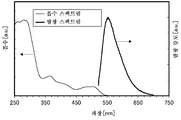
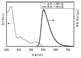
도 10은 구조식(100)으로 나타내어지는 유기 금속 이리듐 복합체의 자외-가시 흡수 스펙트럼 및 발광 스펙트럼을 나타낸 것.
도 11은 발광 소자를 도시한 것.
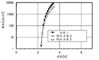
도 12는 발광 소자 1, 비교 발광 소자 2, 및 비교 발광 소자 3의 전압-휘도 특성을 나타낸 것.
도 13은 발광 소자 1, 비교 발광 소자 2, 및 비교 발광 소자 3의 휘도-전류 효율 특성을 나타낸 것.
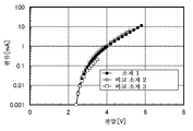
도 14는 발광 소자 1, 비교 발광 소자 2, 및 비교 발광 소자 3의 전압-전류 특성을 나타낸 것.
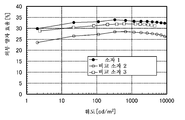
도 15는 발광 소자 1, 비교 발광 소자 2, 및 비교 발광 소자 3의 휘도-외부 양자 효율 특성을 나타낸 것.
도 16은 발광 소자 1, 비교 발광 소자 2, 및 비교 발광 소자 3의 발광 스펙트럼을 나타낸 것.
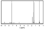
도 17은 구조식(134)으로 나타내어지는 유기 금속 이리듐 복합체의 1H-NMR 차트를 나타낸 것.
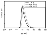
도 18은 구조식(134)으로 나타내어지는 유기 금속 이리듐 복합체의 자외-가시 흡수 스펙트럼 및 발광 스펙트럼을 나타낸 것.Figure 1 shows a model of the atomic arrangement used in the calculation.
Fig. 2 shows calculation results of the back angle between the pyrimidine ring and the phenyl group. Fig.
3 shows a structure of a light emitting element.
4 shows a structure of a light emitting device.
5 (A) and 5 (B) show the structure of the light emitting device, respectively.
6 (A) and 6 (B) show a light emitting device.
7 (A) to 7 (D) show electronic devices, respectively.
8 (A) to 8 (C) show a lighting apparatus and an electronic apparatus.
9 is a 1 H-NMR chart of an organometallic iridium complex represented by the structural formula (100).
10 shows an ultraviolet-visible absorption spectrum and an emission spectrum of an organometallic iridium complex represented by the structural formula (100).
11 shows a light emitting element.
12 shows the voltage-luminance characteristics of the light-emitting
13 shows the luminance-current efficiency characteristics of the light-emitting
14 shows voltage-current characteristics of the light-emitting
15 shows the luminance-external quantum efficiency characteristics of the light-emitting
16 shows the emission spectra of the light-emitting
17 is a 1 H-NMR chart of the organometallic iridium complex represented by the structural formula (134).
18 shows the ultraviolet-visible absorption spectrum and the emission spectrum of the organometallic iridium complex represented by the structural formula (134).
실시형태를 도면을 참조하여 자세히 설명한다. 다만, 본 발명은 이하의 기재에 한정되지 않고, 본 발명의 취지 및 범위로부터 벗어나지 않고, 다양하게 변경 및 변형할 수 있다는 것은, 당업자에 의하여 쉽게 이해된다. 따라서, 본 발명은 이하의 실시형태의 내용에 한정되도록 해석되지 말아야 한다. 또한, 이하에 설명되는 발명의 구조에서, 같은 부분 또는 비슷한 기능을 갖는 부분은 상이한 도면에서 같은 부호로 나타내어지고, 이런 부분의 설명은 반복하지 않는다.Embodiments will be described in detail with reference to the drawings. However, it is to be understood that the present invention is not limited to the following description, and various changes and modifications can be made by those skilled in the art without departing from the spirit and scope of the present invention. Therefore, the present invention should not be construed as being limited to the contents of the following embodiments. In the structure of the invention described below, parts having the same or similar functions are denoted by the same reference numerals in different drawings, and description of these parts is not repeated.
톱 이미션 구조, 보텀 이미션 구조, 및 듀얼 이미션 구조를 본 명세서에 설명되는 발광 소자에 적용할 수 있다.A top emission structure, a bottom emission structure, and a dual emission structure can be applied to the light emitting device described in this specification.
본 명세서 등에서, 유기 금속 이리듐 복합체의 분자 구조에서의 이면각 및 결합각은 Gaussian, Inc.에 의하여 생산된 양자 화학 계산 프로그램을 사용하여 계산된 값이다. 또 다른 양자 화학 계산 프로그램이 본 발명의 일 형태의 유기 금속 이리듐 복합체의 분자 구조를 계산하기 위하여 사용될 때, 계산된 값은 Gaussian, Inc.에 의하여 생산된 상술한 양자 화학 계산 프로그램을 사용하여 얻어진 값과 상이한 경우가 있다. 계산된 값은 양자 화학 계산 프로그램의 계산 조건에 영향될 수도 있다.In the present specification and the like, the back angle and the bonding angle in the molecular structure of the organometallic iridium complex are values calculated using a quantum chemistry calculation program produced by Gaussian, Inc. When another quantum chemistry calculation program is used to calculate the molecular structure of an organometallic iridium complex of an embodiment of the present invention, the calculated value is the value obtained using the quantum chemistry calculation program produced by Gaussian, Inc. . ≪ / RTI > The calculated values may be influenced by the calculation conditions of the quantum chemistry calculation program.
본 명세서 등의 발광 장치는, 이 범주에, 화상 표시 디바이스 및 광원을 포함한다. 발광 장치는, 이하의 모듈을 범주에 포함한다: FPC(flexible printed circuit) 또는 TCP(tape carrier package) 등의 커넥터가 패널에 부착된 모듈, TCP의 끝에 인쇄 배선판이 제공된 모듈; 및 IC(integrated circuit)가 COG(chip on glass) 방식으로 발광 소자에 직접 실장된 모듈이다.Light emitting devices such as the present specification include, in this category, an image display device and a light source. The light emitting device includes the following modules: a module in which a connector such as a flexible printed circuit (FPC) or a tape carrier package (TCP) is attached to a panel, a module in which a printed wiring board is provided at the end of TCP; And an IC (integrated circuit) are directly mounted on a light emitting device by a COG (chip on glass) method.
(실시형태 1)(Embodiment 1)
본 실시형태에서, 본 발명의 형태인 유기 금속 이리듐 복합체를 설명한다.In this embodiment, an organometallic iridium complex in the form of the present invention will be described.
본 발명의 일 형태는 일반식(G1)으로 나타내어지는 구조를 포함하는 유기 금속 이리듐 복합체다.An embodiment of the present invention is an organometallic iridium complex containing a structure represented by the general formula (G1).

일반식(G1)에서, Ar은 6~13개의 탄소 원자를 갖는 치환 또는 비치환된 아릴렌기를 나타낸다. R1~R6은 독립적으로 수소 및 1~6개의 탄소 원자를 갖는 치환 또는 비치환된 알킬기 중 어느 하나를 나타낸다. 또한, R2 및 R6 중 적어도 하나는 1~6개의 탄소 원자를 갖는 알킬기를 나타낸다. X는 탄소 원자 및 질소 원자 중 어느 하나를 나타내고, 상기 탄소 원자는 수소 및 1~6개의 탄소 원자를 갖는 알킬기 중 어느 하나를 갖는다. 피리딘 고리와 R2~R6을 갖는 페닐기 사이의 이면각 또는 피리미딘 고리와 R2~R6을 갖는 페닐기 사이의 이면각은 30° 이상 90° 이하다. R1과 대향하는 피리딘 고리의 내각 또는 R1과 대향하는 피리미딘 고리의 내각은 120°의 ±2°의 범위 내에 있다.In the general formula (G1), Ar represents a substituted or unsubstituted arylene group having 6 to 13 carbon atoms. R 1 to R 6 independently represent hydrogen or a substituted or unsubstituted alkyl group having 1 to 6 carbon atoms. Also, at least one of R 2 and R 6 represents an alkyl group having 1 to 6 carbon atoms. X represents any one of a carbon atom and a nitrogen atom, and the carbon atom has any one of hydrogen and an alkyl group having 1 to 6 carbon atoms. The back angle between the pyridine ring and the phenyl group having R 2 to R 6 or the back angle between the pyrimidine ring and the phenyl group having R 2 to R 6 is 30 ° or more and 90 ° or less. R 1 and the cabinet of the cabinet, or R 1 and the counter pyrimidine ring to the pyridine ring facing is in the range of ± 2 ° of the 120 °.
본 발명의 일 형태는 일반식(G2)으로 나타내어지는 유기 금속 이리듐 복합체다.An embodiment of the present invention is an organometallic iridium complex represented by the general formula (G2).

일반식(G2)에서, R1~R9는 독립적으로 수소 및 1~6개의 탄소 원자를 갖는 치환 또는 비치환된 알킬기 중 어느 하나를 나타낸다. 또한, R2 및 R6 중 적어도 하나는 1~6개의 탄소 원자를 갖는 알킬기를 나타낸다. X는 탄소 원자 및 질소 원자 중 어느 하나를 나타내고, 상기 탄소 원자는 수소 및 1~6개의 탄소 원자를 갖는 알킬기 중 어느 하나를 갖는다. 또한, L은 단일 음이온 배위자를 나타낸다. 피리딘 고리와 R7~R9를 갖는 페닐기 사이의 이면각 또는 피리미딘 고리와 R7~R9를 갖는 페닐기 사이의 이면각은 0° 이상 2° 미만이다. 피리딘 고리와 R2~R6을 갖는 페닐기 사이의 이면각 또는 피리미딘 고리와 R2~R6을 갖는 페닐기 사이의 이면각은 30° 이상 90° 이하다.In formula (G2), R 1 to R 9 independently represent hydrogen or a substituted or unsubstituted alkyl group having 1 to 6 carbon atoms. Also, at least one of R 2 and R 6 represents an alkyl group having 1 to 6 carbon atoms. X represents any one of a carbon atom and a nitrogen atom, and the carbon atom has any one of hydrogen and an alkyl group having 1 to 6 carbon atoms. Further, L represents a single anion ligand. The back angle between the pyridine ring and the phenyl group having R 7 to R 9 or the back angle between the pyrimidine ring and the phenyl group having R 7 to R 9 is 0 ° or more and less than 2 °. The back angle between the pyridine ring and the phenyl group having R 2 to R 6 or the back angle between the pyrimidine ring and the phenyl group having R 2 to R 6 is 30 ° or more and 90 ° or less.
일반식(G1) 또는 일반식(G2)을 참조하여 설명한 바와 같이, 본 발명의 일 형태는 유기 금속 이리듐 복합체의 분자 구조에서의 피리딘 고리 또는 피리미딘 고리와 상기 피리딘 고리 또는 상기 피리미딘 고리에 결합되는 페닐기 사이의 이면각에 의하여 기술적으로 특징짓는다. 피리딘 고리 또는 피리미딘 고리와 상기 피리딘 고리 또는 상기 피리미딘 고리에 결합되는 페닐기 사이의 이면각이 소정의 범위 내에 있기 때문에, 높은 발광 효율 및 긴 수명을 갖는 유기 금속 이리듐 복합체, π-공액이 연장되기 어렵고 높은 발광 효율을 갖는 유기 금속 이리듐 복합체, 또는 고효율로 시감도가 높은 광을 발하는 유기 금속 이리듐 복합체를 제공할 수 있다.As described with reference to the general formula (G1) or the general formula (G2), one form of the present invention relates to a pyridine ring or a pyrimidine ring in the molecular structure of an organometallic iridium complex and a pyridine ring or a pyrimidine ring By the back angle between the phenyl groups. Since the back angle between the pyridine ring or the pyrimidine ring and the phenyl group bonded to the pyridine ring or the pyrimidine ring is within a predetermined range, the organometallic iridium complex having a high luminous efficiency and long life, It is possible to provide an organometallic iridium complex which is difficult and has a high luminous efficiency or an organometallic iridium complex which emits light with high efficiency and high visibility.
여기서, 유기 금속 이리듐 복합체의 분자 구조에서의 피리딘 고리 또는 피리미딘 고리와 상기 피리딘 또는 피리미딘 고리에 결합되는 페닐기 사이의 이면각으로부터, 상기 유기 금속 이리듐 복합체의 삼중항 들뜬 준위가 계산되었다. 구체적으로, 구조식(500)으로 나타내어지는 (아세틸아세토나토)비스(4,6-다이페닐피리미디나토)이리듐(Ⅲ)(약칭: Ir(dppm)2(acac))의 삼중항 준위는 피리미딘 고리와 피리미딘 고리의 6위치에서의 페닐기 사이의 이면각으로부터 계산되었다.Here, the triplet excited states of the organometallic iridium complexes were calculated from the back angle between the pyridine ring or the pyrimidine ring in the molecular structure of the organometallic iridium complex and the phenyl group bonded to the pyridine or pyrimidine ring. Specifically, the triplet level of (acetylacetonato) bis (4,6-diphenylpyrimidinato) iridium (III) (abbreviation: Ir (dppm) 2 (acac)) represented by the structural formula (500) Was calculated from the back angle between the ring and the phenyl group at the 6 position of the pyrimidine ring.

도 1은 계산에 사용된 원자 배열의 모델도를 나타낸 것이다. 도 1에서의 모델도는 Ir(dppm)2(acac)의 일부의 원자 배열을 개략적으로 도시한 것이고, 피리미딘 고리(Pm)와 피리미딘 고리의 6위치에서의 페닐기(Ph) 사이의 이면각을 설명하기 위한 것이다.Fig. 1 shows a model diagram of the atomic arrangement used in the calculation. The schematic diagram of FIG. 1 schematically shows the atomic arrangement of a part of Ir (dppm) 2 (acac), and the angle between the pyrimidine ring (Pm) and the phenyl group (Ph) at the 6-position of the pyrimidine ring .
도 1의 상부에서의 모델도에서, 피리미딘 고리(Pm)와 피리미딘 고리의 6위치에서의 페닐기(Ph) 사이의 이면각(β)은 0°다. 이면각(β)은 도 1의 하부에 나타낸 바와 같이 증가되었고, 유기 금속 이리듐 복합체의 삼중항 준위를 계산하였다. 또한, Ir(dppm)2(acac)에서의, 피리미딘 고리(Pm)와 피리미딘 고리의 6위치에서의 페닐기 사이의 이면각은 10°의 스텝 간격으로 0°로부터 90°까지 변화하였다. 도 1에서, 원자(이리듐 원자(Ir), 탄소 원자(C), 수소 원자(H), 질소 원자(N), 및 산소 원자(O))의 종류를 파선으로 구획짓는 사각에 나타낸다.In the model diagram at the upper part of Fig. 1, the back angle ([beta]) between the pyrimidine ring (Pm) and the phenyl group (Ph) at the 6-position of the pyrimidine ring is 0 [deg.]. The angle of the back surface () increased as shown in the lower part of Fig. 1, and the triplet level of the organometallic iridium complex was calculated. The back angle between the pyrimidine ring (Pm) and the phenyl group at the 6-position of the pyrimidine ring in Ir (dppm) 2 (acac) varied from 0 ° to 90 ° at step intervals of 10 °. In Fig. 1, the kinds of atoms (iridium atom (Ir), carbon atom (C), hydrogen atom (H), nitrogen atom (N), and oxygen atom (O)) are shown by squares dividing by dashed lines.
계산 방법은 이하와 같다. 또한, Gaussian09를 양자 화학 계산 프로그램으로서 사용하였다. 고성능 컴퓨터(SGI Japan, Ltd.제, Altix 4700)를 계산에 사용하였다.The calculation method is as follows. Also, Gaussian09 was used as a quantum chemical calculation program. A high performance computer (Altix 4700, SGI Japan, Ltd.) was used for the calculation.
기본 함수로서, 6-311G(d,p)가 H, C, N, 및 O에 사용되고, Lanl2dz가 Ir에 사용되었다. 범함수로서 B3PW91이 사용되었다. 삼중항 준위는 단일항 및 삼중항 들뜬 상태의 TD-DFT계산에 의하여 계산되었다. 계산의 결과는 도 2에 나타냈다.As a basic function, 6-311G (d, p) is used for H, C, N, and O, and Lanl2dz is used for Ir. B3PW91 was used as a general function. Triplet levels were calculated by TD-DFT calculations of singlet and triplet excited states. The results of the calculation are shown in Fig.
도 2에서의 결과로 나타내어진 바와 같이, Ir(dppm)2(acac)에서의 피리미딘 고리와 피리미딘 고리의 6위치에서의 페닐기 사이의 이면각이 0°일 때, 삼중항 들뜸 에너지는 547nm의 파장에 상당하고, 상기 이면각이 30°일 때, 삼중항 들뜸 에너지는 542nm의 파장에 상당한다. 피리미딘 고리와 피리미딘 고리의 6위치에서의 페닐기 사이의 이면각이 90°일 때, 삼중항 들뜸 에너지는 517nm의 파장에 상당한다. 도 2는 10°의 스텝 간격으로 0°~90°의 이면각을 사용한 계산의 결과를 나타낸 것이다. 구조식(500)으로 나타내어지는 Ir(dppm)2(acac)에서, 피리미딘 고리와 피리미딘 고리의 6위치에서의 페닐기 사이의 이면각은 계산에 의하여 18°가 되는 것을 찾았다. 도 2에서, 삼중항 들뜸 에너지는 파장(nm)으로 변환된다.As shown in Fig. 2, when the back angle between the pyrimidine ring at Ir (dppm) 2 (acac) and the phenyl group at the 6-position of the pyrimidine ring was 0 °, the triplet excitation energy was 547 nm And when the back angle is 30 DEG, the triplet excitation energy corresponds to a wavelength of 542 nm. When the back angle between the phenyl group at the 6-position of the pyrimidine ring and the pyrimidine ring is 90 °, the triplet excitation energy corresponds to a wavelength of 517 nm. Fig. 2 shows the results of calculations using a back angle of 0 [deg.] To 90 [deg.] At step intervals of 10 [deg.]. In the Ir (dppm) 2 (acac) represented by the structural formula (500), the back angle between the phenyl group at the 6-position of the pyrimidine ring and the pyrimidine ring was found to be 18 ° by calculation. In Fig. 2, the triplet excitation energy is converted to the wavelength (nm).
도 2에서의 계산 결과는, 유기 금속 이리듐 복합체에서의 피리미딘 고리와 피리미딘 고리의 6위치에서의 페닐기 사이의 이면각이 30° 이상 90° 이하인 경우, 발광 파장은 유기 금속 이리듐 복합체에서의 피리미딘 고리와 피리미딘 고리의 6위치에서의 페닐기 사이의 이면각이 0°인 경우보다 5nm 이상 30nm 이하만큼 짧아지는 것을 시사한다.The calculation results in Fig. 2 show that when the back angle between the pyrimidine ring and the phenyl group at the 6-position of the pyrimidine ring in the organometallic iridium complex is 30 ° or more and 90 ° or less, It is suggested that the back angle between the phenyl group at the 6-position of the pyridine ring and the pyrimidine ring is shorter than 5 nm to 30 nm or less as compared with the case where the back angle is 0 °.
상술한 바와 같이 유기 금속 이리듐 복합체에서의 피리미딘 고리와 피리미딘 고리의 6위치에서의 페닐기 사이의 이면각이 증가될 때, 즉 유기 금속 이리듐 복합체에서의 피리미딘 고리의 6위치에서의 페닐기가 비틀릴 때, π-공액은 연장되기 어렵고, 발광 파장은 최대로 30nm 정도 저감된다. 이 방법으로, 유기 금속 이리듐 복합체의 발광 파장은 유기 금속 이리듐 복합체에서의 피리딘 고리 또는 피리미딘 고리에 결합되는 치환기에 의하여 형성된 이면각(여기서는 피리미딘 고리의 6위치에서의 페닐기에 의하여 형성되는 이면각)에 의존한다.As described above, when the back angle between the pyrimidine ring in the organometallic iridium complex and the phenyl group at the 6-position of the pyrimidine ring is increased, that is, when the phenyl group at the 6-position of the pyrimidine ring in the organometallic iridium complex is non- When it is wrong, the? -Conjugate is difficult to elongate, and the emission wavelength is reduced by about 30 nm at the maximum. In this way, the emission wavelength of the organometallic iridium complex is determined by the angle of the back surface formed by the substituent bonded to the pyridine ring or the pyrimidine ring in the organometallic iridium complex (here, the angle of the back surface formed by the phenyl group at the 6 position of the pyrimidine ring ).
또한, 도 1에서의 모델도에서, 유기 금속 이리듐 복합체에서의 피리미딘 고리의 6위치에서의 페닐기에 의하여 형성되는 이면각을 변화시킬 수 있기 위하여, 피리미딘 고리 또는 상기 피리미딘 고리의 6위치에 결합된 페닐기에 치환기는 결합되지 않는다. 실제의 유기 금속 이리듐 복합체에서 피리딘 또는 피리미딘 고리, 또는 상기 피리딘 또는 피리미딘 고리에 결합된 페닐기에 대한 치환기의 결합은, 유기 금속 이리듐 복합체의 분자 구조에서의 피리딘 또는 피리미딘 고리와 상기 피리딘 또는 피리미딘 고리에 결합된 페닐기 사이의 이면각을 변화시킬 수 있다. 하지만, 치환기에 따라서는, 피리딘 고리 또는 피리미딘 고리가 일그러질 수 있다.Further, in the model diagram in Fig. 1, in order to change the back angle formed by the phenyl group at the 6-position of the pyrimidine ring in the organometallic iridium complex, the pyrimidine ring or the pyrimidine ring at the 6-position The substituent is not bonded to the bonded phenyl group. In the actual organometallic iridium complex, the substitution of a substituent for a pyridine or pyrimidine ring or for a phenyl group bonded to the pyridine or pyrimidine ring is carried out by reacting a pyridine or pyrimidine ring in the molecular structure of the organometallic iridium complex with the pyridine or pyrimidine ring It is possible to change the angle of the back surface between the phenyl group bonded to the imine ring. However, depending on the substituent, a pyridine ring or a pyrimidine ring may be substituted.
여기서, 구조식(501), 구조식(500), 구조식(100), 구조식(502), 구조식(503), 및 구조식(504)으로 나타내어지는 각 유기 금속 이리듐 복합체의 결합각 및 이면각을 계산하였다.Herein, the bonding angle and the back angle of each organometallic iridium complex represented by the structural formula (501), the structural formula (500), the structural formula (100), the structural formula (502), the structural formula (503), and the structural formula (504) were calculated.


또한, 구조식(501)으로 나타내어지는 유기 금속 이리듐 복합체는 비스(2-페닐피리디나토-N,C 2')이리듐(III)아세틸아세토네이트(약칭: Ir(ppy)2(acac))다. 구조식(500)으로 나타내어지는 유기 금속 이리듐 복합체는 Ir(dppm)2(acac)다. 구조식(100)으로 나타내어지는 유기 금속 이리듐 복합체는 비스{2-[6-(2,6-다이메틸페닐)-4-피리미딘일-κN3]페닐-κC}(2,4-펜탄다이오나토-κO,O')이리듐(III)(약칭: Ir(ppm-dmp)2(acac))이다. 구조식(502)으로 나타내어지는 유기 금속 이리듐 복합체는 (아세틸아세토나토)비스[5-메틸-6-(2-메틸페닐)-4-페닐피리미디나토]이리듐(III)(별명: 비스{2-[5-메틸-6-(2-메틸페닐)-4-피리미딘일-κN3]페닐-κC}(2,4-펜탄다이오나토-κ2 O,O')이리듐(III))(약칭: Ir(mpmppm)2(acac))이다. 구조식(503)으로 나타내어지는 유기 금속 이리듐 복합체는 (아세틸아세토나토)비스(4,5,6-트라이페닐피리미디나토)이리듐(III)(별명: 비스[2-(5,6-다이페닐-4-피리미딘일-κN3)페닐-κC](2,4-펜탄다이오나토-κ2 O,O')이리듐(III))(약칭: Ir(tppm)2(acac))이다. 구조식(504)으로 나타내어지는 유기 금속 이리듐 복합체는 비스[2-(5-페닐-4-피리미딘일-κN3)페닐-κC](2,4-펜탄다이오나토-κ2 O,O')이리듐(III)(약칭: Ir(5dppm)2(acac))이다.The organometallic iridium complex represented by the structural formula (501) is bis (2-phenylpyridinato- N , C 2 ' ) iridium (III) acetylacetonate (abbreviation: Ir (ppy) 2 (acac)). The organometallic iridium complex represented by the structural formula (500) is Ir (dppm) 2 (acac). Organometallic iridium complexes represented by the following structural formula (100) bis {2- [6- (2,6-dimethylphenyl) -4-pyrimidinyl -κ N 3] phenyl} -κ C (2,4- pentane diode Nato-κ O , O ') iridium (III) (abbreviation: Ir (ppm-dmp) 2 (acac)). The organometallic iridium complex represented by the structural formula (502) can be produced by reacting (acetylacetonato) bis [5-methyl-6- (2-methylphenyl) -4- phenylpyrimidinato] iridium (III) 5-methyl-6- (2-methylphenyl) -4-pyrimidinyl -κ N 3] phenyl} -κ C (2,4- pentane diode NATO -κ 2 O, O ') iridium (III)) (abbreviated : Ir (mpmppm) 2 (acac)). The organometallic iridium complex represented by the structural formula (503) is obtained by reacting (acetylacetonato) bis (4,5,6-triphenylpyrimidinato) iridium (III) (also called bis [2- (5,6- is Ir (tppm) 2 (acac) ): 4- pyrimidinyl -κ N 3) phenyl -κ C] (2,4- pentane diode NATO -κ 2 O, O ') iridium (III)) (abbreviated. Organometallic iridium complexes represented by the following structural formula (504) is bis [2- (5-phenyl-4-pyrimidinyl -κ N 3) phenyl -κ C] (2,4- pentane diode NATO -κ 2 O, O ') Iridium (III) (abbreviation: Ir (5 dppm) 2 (acac)).
계산 방법은 이하와 같다. 또한, Gaussian09를 양자 화학 계산 프로그램으로서 사용하였다. 고성능 컴퓨터(SGI Japan, Ltd.제, Altix 4700)를 계산에 사용하였다.The calculation method is as follows. Also, Gaussian09 was used as a quantum chemical calculation program. A high performance computer (Altix 4700, SGI Japan, Ltd.) was used for the calculation.
기본 함수로서, 6-311G(d,p)가 H, C, N, 및 O에 사용되고, Lanl2dz가 Ir에 사용되었다. 범함수로서 B3PW91이 사용되었다.As a basic function, 6-311G (d, p) is used for H, C, N, and O, and Lanl2dz is used for Ir. B3PW91 was used as a general function.
구조식(501), 구조식(500), 구조식(100), 구조식(502), 구조식(503), 및 구조식(504)으로 나타내어지는 유기 금속 이리듐 복합체의 결합각 및 이면각으로서, 구조식(600)으로 나타내어지는 분자 구조의 결합각(α1 및 α2), 내각(α3), 및 이면각(β2)을 계산하였다. 구조식(501), 구조식(500), 구조식(100), 구조식(502), 구조식(503), 및 구조식(504)으로 나타내어지는 유기 금속 이리듐 복합체는 구조식(600)으로 나타내어지는 분자 구조를 공통으로 갖는다.As the bonding angle and the back angle of the organometallic iridium complex represented by Structural Formula (501), Structural Formula (500), Structural Formula (100), Structural Formula (502), Structural Formula (503), and Structural Formula (504) The coupling angles (α 1 and α 2 ), the internal angle (α 3 ), and the back angle (β 2 ) of the molecular structures represented were calculated. The organometallic iridium complex represented by the structural formula (501), the structural formula (500), the structural formula (100), the structural formula (502), the structural formula (503), and the structural formula (504) .

구조식(600)에서, α1로 나타내어지는 결합각은 피리딘 고리의 2위치에서의 페닐기의 외각이고; α2로 나타내어지는 결합각은 피리딘 고리의 2위치에서의 외각이고, α3은 피리딘 고리의 3위치에서의 내각을 나타내고; β2는 피리딘 고리와 이 피리딘 고리의 2위치에서의 페닐기 사이의 이면각을 나타낸다. 또한, 이해하기 쉽게 하기 위하여 구조식(600)에서 결합각(α1 및 α2), 내각(α3), 및 이면각(β2)의 설명에 피리딘 고리를 사용하였지만, 피리미딘 고리에 결합각(α1 및 α2), 내각(α3), 및 이면각(β2)을 적용할 수도 있다. 또한, 피리미딘 고리의 경우, 페닐기의 치환기의 위치는 피리미딘 고리의 4위치다.In structural formula (600), the bonding angle represented by? 1 is the outer angle of the phenyl group at the 2-position of the pyridine ring; the bonding angle represented by? 2 is the outer angle at the 2-position of the pyridine ring,? 3 represents the inner angle at the 3-position of the pyridine ring; ? 2 represents the back angle between the pyridine ring and the phenyl group at the 2-position of the pyridine ring. Also, for ease of understanding, the pyridine rings are used in the description of the bonding angles (α 1 and α 2 ), the inner angle (α 3 ), and the back angle (β 2 ) in the structural formula (600) (? 1 and? 2 ), the inner angle? 3 , and the back angle? 2 may be applied. Further, in the case of the pyrimidine ring, the substituent position of the phenyl group is at the 4-position of the pyrimidine ring.
계산 결과를 표 1에 나타낸다.Table 1 shows the calculation results.
표 1에 나타낸 바와 같이, 구조식(501), 구조식(500), 및 구조식(100)에서, 각도(α1)는 120° 이상 124° 미만이다. 구조식(502), 구조식(503), 및 구조식(504)에서, 각도(α1)는 124° 이상이다. 구조식(501), 구조식(500), 및 구조식(100)에서, 각도(α2)는 120° 이상 129° 미만이다. 구조식(502), 구조식(503), 및 구조식(504)에서, 각도(α2)는 129° 이상이다. 구조식(501), 구조식(500), 및 구조식(100)에서, 각도(α3)는 120°의 ±2°의 범위 내에 있는 한편, 구조식(502), 구조식(503), 및 구조식(504)에서, 각도(α3)는 120°의 ±2°의 범위 외에 있다. 구조식(501), 구조식(500), 및 구조식(100)에서, 이면각(β2)은 0° 이상 2° 이하인 한편 구조식(502), 구조식(503), 및 구조식(504)에서, 이면각(β2)은 2° 이상이다.As shown in Table 1, in Structural Formula (501), Structural Formula (500), and Structural Formula (100), angle? 1 is 120 degrees or more and less than 124 degrees. In formulas (502), (503), and (504), angle (? 1 ) is greater than or equal to 124 degrees. In Structural Formula (501), Structural Formula (500), and Structural Formula (100), angle? 2 is not less than 120 degrees and less than 129 degrees. In formulas (502), (503), and (504), angle (? 2 ) is greater than 129 degrees. In the structural formula (501), formula (500), and Structural Formula (100), the angle (α 3) is in the range of ± 2 ° of the 120 ° On the other hand, the structural formula (502), formula (503), and Structural Formula (504) The angle [alpha] 3 is out of the range of +/- 2 [deg.] Of 120 [deg.]. In Structural Formula (502), Structural Formula (503), and Structural Formula (504), the back angle (? 2 ) (beta 2 ) is at least 2 degrees.
상술한 바와 같이, 피리딘 고리 또는 피리미딘 고리에 결합된 치환기의 위치 또는 종류에 따라 피리딘 고리 또는 피리미딘 고리의 형상은 변화된다. 바꿔 말하면, 피리딘 고리 또는 피리미딘 고리의 분자 구조가 일그러진다. 표 1에 나타낸 바와 같이, 구조식(501), 구조식(500), 및 구조식(100)으로 나타내어지는 유기 금속 이리듐 복합체에서, 피리딘 고리 또는 피리미딘 고리의 분자 구조 일그러짐은 굉장히 작다. 한편, 구조식(502), 구조식(503), 및 구조식(504)으로 나타내어지는 유기 금속 이리듐 복합체 각각에서, 피리딘 고리 또는 피리미딘 고리의 분자 구조 일그러짐은 크다. 표 1에 나타낸 바와 같이 피리딘 고리 또는 피리미딘 고리의 분자 구조 일그러짐은 각도(α1~α3) 및 이면각(β2) 중 어느 하나를 계산함으로써 찾아낼 수 있다. 또한, 피리딘 고리 또는 피리미딘 고리의 분자 구조 일그러짐이 클 때, 양자 효율을 높일 수 없는 경우가 있다.As described above, depending on the position or kind of the substituent bonded to the pyridine ring or the pyrimidine ring, the shape of the pyridine ring or the pyrimidine ring is changed. In other words, the molecular structure of the pyridine ring or the pyrimidine ring is distorted. As shown in Table 1, in the organometallic iridium complex represented by Structural Formula (501), Structural Formula (500), and Structural Formula (100), the molecular structure distortion of the pyridine ring or pyrimidine ring is extremely small. On the other hand, in each of the organometallic iridium complexes represented by the structural formulas (502), (503), and (504), the molecular structure distortion of the pyridine ring or the pyrimidine ring is large. As shown in Table 1, the molecular structure distortion of the pyridine ring or the pyrimidine ring can be found by calculating any one of the angles (α 1 to α 3 ) and the back angle (β 2 ). Further, when the molecular structure distortion of the pyridine ring or the pyrimidine ring is large, the quantum efficiency may not be enhanced in some cases.
상술한 관점에서, 본 발명의 일 형태에서, 페닐기는 일반식(G1) 또는 일반식(G2)에 도시된 바와 같이, 유기 금속 이리듐 복합체에서의 피리딘 고리 또는 피리미딘 고리의 소정의 위치에서 결합된다. 또한, 유기 금속 이리듐 복합체에서 피리딘 고리 또는 피리미딘 고리에 결합된 페닐기에 의하여 형성된 이면각은 소정의 범위 내에 있다. 따라서 π-공액의 연장이 억제되어 유기 금속 이리듐 복합체로부터 발해진 광의 파장은 짧게 된다. 또한, 피리딘 고리 또는 피리미딘 고리의 분자 구조 일그러짐이 억제됨으로써 높은 양자 효율을 달성할 수 있다.In view of the above, in one aspect of the present invention, the phenyl group is bonded at a predetermined position of the pyridine ring or the pyrimidine ring in the organometallic iridium complex, as shown in the general formula (G1) or the general formula (G2) . Further, the back angle formed by the phenyl group bonded to the pyridine ring or the pyrimidine ring in the organometallic iridium complex is within a predetermined range. Therefore, the extension of the? -Conjugate is suppressed and the wavelength of the light emitted from the organometallic iridium complex is shortened. Further, the molecular structure distortion of the pyridine ring or the pyrimidine ring is suppressed, so that high quantum efficiency can be achieved.
본 발명의 일 형태의 유기 금속 이리듐 복합체의 구조는 일반식(G1) 및 일반식(G2)뿐만 아니라 이하에 나타낸 식에 의해서도 나타내어질 수 있다.The structure of the organometallic iridium complex of one embodiment of the present invention can be represented not only by the general formulas (G1) and (G2) but also by the following formulas.
본 발명의 일 형태는 일반식(G3)으로 나타내어지는 유기 금속 이리듐 복합체다.An embodiment of the present invention is an organometallic iridium complex represented by the general formula (G3).

일반식(G3)에서, R1, R2, 및 R6~R9는 독립적으로 수소 및 1~6개의 탄소 원자를 갖는 치환 또는 비치환된 알킬기 중 어느 하나를 나타낸다. 또한, R2 및 R6 중 적어도 하나는 1~6개의 탄소 원자를 갖는 알킬기를 나타낸다. X는 탄소 원자 및 질소 원자 중 어느 하나를 나타내고, 상기 탄소 원자는 수소 및 1~6개의 탄소 원자를 갖는 알킬기 중 어느 하나를 갖는다. 또한, L은 단일 음이온 배위자를 나타낸다. 피리딘 고리와 R7~R9를 갖는 페닐기 사이의 이면각 또는 피리미딘 고리와 R7~R9를 갖는 페닐기 사이의 이면각은 0° 이상 2° 미만이다. 피리딘 고리와 R2 및 R6을 갖는 페닐기 사이의 이면각 또는 피리미딘 고리와 R2 및 R6을 갖는 페닐기 사이의 이면각은 30° 이상 90° 이하다.In formula (G3), R 1 , R 2 , and R 6 to R 9 independently represent hydrogen or a substituted or unsubstituted alkyl group having 1 to 6 carbon atoms. Also, at least one of R 2 and R 6 represents an alkyl group having 1 to 6 carbon atoms. X represents any one of a carbon atom and a nitrogen atom, and the carbon atom has any one of hydrogen and an alkyl group having 1 to 6 carbon atoms. Further, L represents a single anion ligand. The back angle between the pyridine ring and the phenyl group having R 7 to R 9 or the back angle between the pyrimidine ring and the phenyl group having R 7 to R 9 is 0 ° or more and less than 2 °. The back angle between the pyridine ring and the phenyl group having R 2 and R 6 or the back angle between the pyrimidine ring and the phenyl group having R 2 and R 6 is 30 ° or more and 90 ° or less.
본 발명의 일 형태는 일반식(G4)으로 나타내어지는 유기 금속 이리듐 복합체다.An embodiment of the present invention is an organometallic iridium complex represented by the general formula (G4).

일반식(G4)에서, R1, R2, 및 R6~R9는 독립적으로 수소 및 1~6개의 탄소 원자를 갖는 치환 또는 비치환된 알킬기 중 어느 하나를 나타낸다. 또한, R2 및 R6 중 적어도 하나는 1~6개의 탄소 원자를 갖는 알킬기를 나타낸다. X는 탄소 원자 및 질소 원자 중 어느 하나를 나타내고, 상기 탄소 원자는 수소 및 1~6개의 탄소 원자를 갖는 알킬기 중 어느 하나를 갖는다. 피리딘 고리와 R7~R9를 갖는 페닐기 사이의 이면각 또는 피리미딘 고리와 R7~R9를 갖는 페닐기 사이의 이면각은 0° 이상 2° 미만이다. 피리딘 고리와 R2 및 R6을 갖는 페닐기 사이의 이면각 또는 피리미딘 고리와 R2 및 R6을 갖는 페닐기 사이의 이면각은 30° 이상 90° 이하다.In the general formula (G4), R 1 , R 2 , and R 6 to R 9 independently represent any one of hydrogen and a substituted or unsubstituted alkyl group having 1 to 6 carbon atoms. Also, at least one of R 2 and R 6 represents an alkyl group having 1 to 6 carbon atoms. X represents any one of a carbon atom and a nitrogen atom, and the carbon atom has any one of hydrogen and an alkyl group having 1 to 6 carbon atoms. The back angle between the pyridine ring and the phenyl group having R 7 to R 9 or the back angle between the pyrimidine ring and the phenyl group having R 7 to R 9 is 0 ° or more and less than 2 °. The back angle between the pyridine ring and the phenyl group having R 2 and R 6 or the back angle between the pyrimidine ring and the phenyl group having R 2 and R 6 is 30 ° or more and 90 ° or less.
본 발명의 일 형태는 일반식(G5)으로 나타내어지는 유기 금속 이리듐 복합체다.An embodiment of the present invention is an organometallic iridium complex represented by the general formula (G5).

일반식(G5)에서, R1~R9는 독립적으로 수소 및 1~6개의 탄소 원자를 갖는 치환 또는 비치환된 알킬기 중 어느 하나를 나타낸다. 또한, R2 및 R6 중 적어도 하나는 1~6개의 탄소 원자를 갖는 알킬기를 나타낸다. X는 탄소 원자 및 질소 원자 중 어느 하나를 나타내고, 상기 탄소 원자는 수소 및 1~6개의 탄소 원자를 갖는 알킬기 중 어느 하나를 갖는다. 또한, L은 단일 음이온 배위자를 나타낸다. α로 나타낸 결합각은 120° 이상 129° 미만이다. 피리딘 고리와 R2~R6을 갖는 페닐기 사이의 이면각 또는 피리미딘 고리와 R2~R6을 갖는 페닐기 사이의 이면각은 30° 이상 90° 이하다.In the general formula (G5), R 1 to R 9 independently represent any one of hydrogen and a substituted or unsubstituted alkyl group having 1 to 6 carbon atoms. Also, at least one of R 2 and R 6 represents an alkyl group having 1 to 6 carbon atoms. X represents any one of a carbon atom and a nitrogen atom, and the carbon atom has any one of hydrogen and an alkyl group having 1 to 6 carbon atoms. Further, L represents a single anion ligand. The coupling angle represented by? is not less than 120 degrees and less than 129 degrees. The back angle between the pyridine ring and the phenyl group having R 2 to R 6 or the back angle between the pyrimidine ring and the phenyl group having R 2 to R 6 is 30 ° or more and 90 ° or less.
본 발명의 일 형태는 일반식(G6)으로 나타내어지는 유기 금속 이리듐 복합체다.An embodiment of the present invention is an organometallic iridium complex represented by the general formula (G6).

일반식(G6)에서, R1, R2, 및 R6~R9는 독립적으로 수소 및 1~6개의 탄소 원자를 갖는 치환 또는 비치환된 알킬기 중 어느 하나를 나타낸다. 또한, R2 및 R6 중 적어도 하나는 1~6개의 탄소 원자를 갖는 알킬기를 나타낸다. X는 탄소 원자 및 질소 원자 중 어느 하나를 나타내고, 상기 탄소 원자는 수소 및 1~6개의 탄소 원자를 갖는 알킬기 중 어느 하나를 갖는다. 또한, L은 단일 음이온 배위자를 나타낸다. 식에서 α로 나타낸 결합각은 120° 이상 129° 미만이다. 피리딘 고리와 R2 및 R6을 갖는 페닐기 사이의 이면각 또는 피리미딘 고리와 R2 및 R6을 갖는 페닐기 사이의 이면각은 30° 이상 90° 이하다.In formula (G6), R 1 , R 2 , and R 6 to R 9 independently represent hydrogen or a substituted or unsubstituted alkyl group having 1 to 6 carbon atoms. Also, at least one of R 2 and R 6 represents an alkyl group having 1 to 6 carbon atoms. X represents any one of a carbon atom and a nitrogen atom, and the carbon atom has any one of hydrogen and an alkyl group having 1 to 6 carbon atoms. Further, L represents a single anion ligand. In the equation, the angle of attachment represented by a is 120 ° or more and less than 129 °. The back angle between the pyridine ring and the phenyl group having R 2 and R 6 or the back angle between the pyrimidine ring and the phenyl group having R 2 and R 6 is 30 ° or more and 90 ° or less.
본 발명의 일 형태는 일반식(G7)으로 나타내어지는 유기 금속 이리듐 복합체다.An embodiment of the present invention is an organometallic iridium complex represented by the general formula (G7).

일반식(G7)에서, R1, R2, 및 R6~R9는 독립적으로 수소 및 1~6개의 탄소 원자를 갖는 치환 또는 비치환된 알킬기 중 어느 하나를 나타낸다. 또한, R2 및 R6 중 적어도 하나는 1~6개의 탄소 원자를 갖는 알킬기를 나타낸다. X는 탄소 원자 및 질소 원자 중 어느 하나를 나타내고, 상기 탄소 원자는 수소 및 1~6개의 탄소 원자를 갖는 알킬기 중 어느 하나를 갖는다. 식에서 α로 나타낸 결합각은 120° 이상 129° 미만이다. 피리딘 고리와 R2 및 R6을 갖는 페닐기 사이의 이면각 또는 피리미딘 고리와 R2 및 R6을 갖는 페닐기 사이의 이면각은 30° 이상 90° 이하다.In formula (G7), R 1 , R 2 , and R 6 to R 9 independently represent hydrogen or a substituted or unsubstituted alkyl group having 1 to 6 carbon atoms. Also, at least one of R 2 and R 6 represents an alkyl group having 1 to 6 carbon atoms. X represents any one of a carbon atom and a nitrogen atom, and the carbon atom has any one of hydrogen and an alkyl group having 1 to 6 carbon atoms. In the equation, the angle of attachment represented by a is 120 ° or more and less than 129 °. The back angle between the pyridine ring and the phenyl group having R 2 and R 6 or the back angle between the pyrimidine ring and the phenyl group having R 2 and R 6 is 30 ° or more and 90 ° or less.
일반식(G1)~일반식(G7) 각각에서, R2 및 R6 중 적어도 하나가 알킬기를 나타내는 것이 바람직하고, 양쪽이 알킬기를 나타내는 것이 더 바람직하다. 이 구조에 의하여, 피리딘 또는 피리미딘 고리와 페닐기 사이의 공액 결합에 의하여 일어나는 넓은 전자 확산을 방지할 수 있다. R2 및 R6 양쪽이 알킬기를 나타내는 구조에서, 피리딘 또는 피리미딘 고리와 R2 및 R6을 갖는 페닐기 사이의 이면각을 크게 할 수 있다.In each of formulas (G1) to (G7), it is preferable that at least one of R 2 and R 6 represents an alkyl group, and it is more preferable that both represent an alkyl group. By this structure, it is possible to prevent broad electron diffusion caused by the conjugated bond between the pyridine or pyrimidine ring and the phenyl group. In the structure in which both R 2 and R 6 represent an alkyl group, the back angle between the pyridine or pyrimidine ring and the phenyl group having R 2 and R 6 can be increased.
일반식(G1)을 참조하여 설명된 바와 같이, R1과 대향하는 피리딘 고리의 내각, 또는 R1과 대향하는 피리미딘 고리의 내각이 120°의 ±2°의 범위 내에 있을 때, 피리딘 고리 또는 피리미딘 고리의 분자 구조 일그러짐을 방지할 수 있다. 일반식(G5)~일반식(G7)을 참조하여 설명된 바와 같이, α로 나타낸 결합각이 120° 이상 129° 미만일 때, 피리딘 고리 또는 피리미딘 고리의 분자 구조 일그러짐을 방지할 수 있다.As explained with reference to the general formula (G1), when the cabinet of the R 1 and the counter pyridine cabinet, or R 1 and the counter pyrimidine ring to the ring to be in the range of ± 2 ° on 120 °, a pyridine ring, or The molecular structure of the pyrimidine ring can be prevented from being distorted. As described with reference to the general formulas (G5) to (G7), molecular structure distortion of the pyridine ring or the pyrimidine ring can be prevented when the bonding angle represented by? Is 120 deg. Or more and less than 129 deg.
이와 같이, 일반식(G1)~일반식(G7)으로 나타내어지는 본 발명의 실시형태의 유기 금속 이리듐 복합체에서, 피리딘 또는 피리미딘 고리와 상기 피리딘 또는 피리미딘 고리에 결합된 페닐기 사이의 이면각 또는 결합각은 소정의 범위 내에 있어, 피리딘 고리 또는 피리미딘 고리의 분자 구조 일그러짐을 방지할 수 있거나, 또는 피리딘 또는 피리미딘 고리와 페닐기 사이의 π-공액의 연장은 입체 장애에 의하여 형성된 비틀림으로 방지될 수 있다. 따라서 유기 금속 이리듐 복합체 각각의 발광 스펙트럼은 짧은 파장 측으로 이동할 수 있다. 또한, 더 높은 효율을 달성할 수 있다.Thus, in the organometallic iridium complex of the embodiment of the present invention represented by the general formula (G1) to the general formula (G7), the surface angle between the pyridine or pyrimidine ring and the phenyl group bonded to the pyridine or pyrimidine ring or The bonding angle is within a predetermined range to prevent the molecular structure distortion of the pyridine ring or the pyrimidine ring or the extension of the pi-conjugation between the pyridine or pyrimidine ring and the phenyl group is prevented by twisting formed by the steric hindrance . Therefore, the emission spectrum of each of the organometallic iridium complexes can be shifted to the shorter wavelength side. In addition, higher efficiency can be achieved.
일반식(G1)~일반식(G7)으로 나타내어지는 본 발명의 실시형태의 유기 금속 이리듐 복합체 각각에서, 금속 이리듐과 배위자가 금속-탄소 결합을 형성하여 전하가 금속으로부터 배위자의 피리딘 또는 피리미딘 고리로 쉽게 천이한다(MLCT(metal to ligand charge transfer) 천이가 쉽게 일어난다). 결과적으로 금지 천이인 인광이 쉽게 일어나고, 삼중항 들뜸 수명이 짧아지고, 상기 유기 금속 이리듐 복합체의 발광 효율이 증가될 수 있다.In each of the organometallic iridium complexes of the embodiments of the present invention represented by the general formulas (G1) to (G7), the metal iridium and the ligand form a metal-carbon bond so that the charge is transferred from the metal to the pyridine or pyrimidine ring (MLCT (metal to ligand charge transfer) transition easily occurs). As a result, phosphorescence which is a prohibited transition easily occurs, triplet excitation lifetime is shortened, and the luminous efficiency of the organometallic iridium complex can be increased.
또한, 일반식(G2), 일반식(G3), 일반식(G5), 또는 일반식(G6)에서, 단일 음이온 배위자는 일반식(L1)~일반식(L7) 중 어느 것에 의하여 나타내어질 수 있다. 단일 음이온 배위자가 일반식(L1)으로 나타내어지는 구조, 즉 베타-다이케톤을 포함하는 구조를 갖는 것이 특히 바람직하다. 단일 음이온 배위자가 일반식(G4) 및 일반식(G7)에 도시된 바와 같은 아세틸아세톤을 포함하는 구조를 갖는 것이 더 바람직하다. 단일 음이온 배위자가 베타-다이케톤 또는 아세틸아세톤을 포함하는 구조를 가질 때, 발광 파장을 저감할 수 있다.In the general formula (G2), the general formula (G3), the general formula (G5) or the general formula (G6), the single anion ligand may be represented by any one of the general formulas (L1) to have. It is particularly preferable that the single anion ligand has a structure represented by the general formula (L1), that is, a structure containing a beta-diketone. It is more preferable that the single anion ligand has a structure including acetylacetone as shown in the general formula (G4) and the general formula (G7). When the single anion ligand has a structure containing beta-diketone or acetylacetone, the emission wavelength can be reduced.


일반식(L1)~일반식(L7)에서, R71∼R109는 독립적으로 수소, 1~6개의 탄소 원자를 갖는 치환 또는 비치환된 알킬기, 할로젠, 바이닐기, 1~6개의 탄소 원자를 갖는 치환 또는 비치환된 할로알킬기, 1~6개의 탄소 원자를 갖는 치환 또는 비치환된 알콕시기, 및 1~6개의 탄소 원자를 갖는 치환 또는 비치환된 알킬싸이오기 중 어느 하나를 나타낸다. 또한, A1∼A3은 독립적으로 질소, 및 수소 또는 치환기 R에 결합된 탄소 중 어느 하나를 나타낸다. 치환기 R은 1~6개의 탄소 원자를 갖는 알킬기, 할로젠, 1~6개의 탄소 원자를 갖는 할로알킬기, 및 페닐기 중 어느 하나다.In the general formulas (L1) to (L7), R 71 to R 109 independently represent hydrogen, a substituted or unsubstituted alkyl group having 1 to 6 carbon atoms, a halogen, a vinyl group, , A substituted or unsubstituted alkylthio group having 1 to 6 carbon atoms, a substituted or unsubstituted alkylthio group having 1 to 6 carbon atoms, a substituted or unsubstituted alkylthio group having 1 to 6 carbon atoms, In addition, A 1 to A 3 independently represent any of nitrogen, and hydrogen or carbon bonded to substituent R. The substituent R is any one of an alkyl group having 1 to 6 carbon atoms, a halogen, a haloalkyl group having 1 to 6 carbon atoms, and a phenyl group.
다음에, 상술한 본 발명의 실시형태의 유기 금속 이리듐 복합체의 구체적인 구조식을 나타낸다(구조식(100)~구조식(134)). 하지만 본 발명의 일 형태는 이에 한정되지 않는다.Next, specific structural formulas of the organometallic iridium complex of the embodiment of the present invention described above (structural formulas (100) to (134)) are shown. However, an embodiment of the present invention is not limited to this.


또한, 구조식(100)~구조식(134)으로 나타내어지는 유기 금속 이리듐 복합체는 인광을 발할 수 있는 신규 물질이다. 배위자의 형태에 따라 이들 물질의 기하 이성질체 및 입체 이성질체가 있을 수 있다. 본 발명의 일 형태의 유기 금속 이리듐 복합체에는 이들 이성질체 모두가 포함된다.Further, the organometallic iridium complex represented by the structural formulas (100) to (134) is a novel substance capable of emitting phosphorescence. Depending on the form of the ligand, there can be geometric isomers and stereoisomers of these materials. An organometallic iridium complex of one form of the present invention includes all of these isomers.
다음에 일반식(G2)으로 나타내어지는 유기 금속 이리듐 복합체를 합성하기 위한 방법의 예를 설명한다.Next, an example of a method for synthesizing an organometallic iridium complex represented by the general formula (G2) will be described.
≪일반식(G0)으로 나타내어지는 피리딘 유도체 또는 피리미딘 유도체를 합성하기 위한 방법≫≪ Process for synthesizing a pyridine derivative or a pyrimidine derivative represented by the general formula (G0) >
먼저, 일반식(G0)으로 나타내어지는 피리딘 유도체 또는 피리미딘 유도체를 합성하기 위한 방법의 예를 설명한다.First, an example of a method for synthesizing a pyridine derivative or a pyrimidine derivative represented by the general formula (G0) will be described.

일반식(G0)에서, R1~R9는 독립적으로 수소 및 1~6개의 탄소 원자를 갖는 치환 또는 비치환된 알킬기 중 어느 하나를 나타낸다. 또한, R2 및 R6 중 적어도 하나는 1~6개의 탄소 원자를 갖는 알킬기를 나타낸다. X는 탄소 원자 및 질소 원자 중 어느 하나를 나타내고, 상기 탄소 원자는 수소 및 1~6개의 탄소 원자를 갖는 알킬기 중 어느 하나를 갖는다. 피리딘 고리와 R7~R9를 갖는 페닐기 사이의 이면각 또는 피리미딘 고리와 R7~R9를 갖는 페닐기 사이의 이면각은 0° 이상 2° 미만이다. 피리딘 고리와 R2~R6을 갖는 페닐기 사이의 이면각 또는 피리미딘 고리와 R2~R6을 갖는 페닐기 사이의 이면각은 30° 이상 90° 이하다.In formula (G0), R 1 to R 9 independently represent hydrogen or a substituted or unsubstituted alkyl group having 1 to 6 carbon atoms. Also, at least one of R 2 and R 6 represents an alkyl group having 1 to 6 carbon atoms. X represents any one of a carbon atom and a nitrogen atom, and the carbon atom has any one of hydrogen and an alkyl group having 1 to 6 carbon atoms. The back angle between the pyridine ring and the phenyl group having R 7 to R 9 or the back angle between the pyrimidine ring and the phenyl group having R 7 to R 9 is 0 ° or more and less than 2 °. The back angle between the pyridine ring and the phenyl group having R 2 to R 6 or the back angle between the pyrimidine ring and the phenyl group having R 2 to R 6 is 30 ° or more and 90 ° or less.
일반식(G0)으로 나타내어지는 피리딘 유도체 또는 피리미딘 유도체의 합성 스킴(A)을 이하에 나타낸다.The synthesis scheme (A) of a pyridine derivative or a pyrimidine derivative represented by the general formula (G0) is shown below.

합성 스킴(A)에서, R1~R9는 독립적으로 수소 및 1~6개의 탄소 원자를 갖는 치환 또는 비치환된 알킬기 중 어느 하나를 나타낸다. 또한, R2 및 R6 중 적어도 하나는 1~6개의 탄소 원자를 갖는 알킬기를 나타낸다. X는 탄소 원자 및 질소 원자 중 어느 하나를 나타내고, 상기 탄소 원자는 수소 및 1~6개의 탄소 원자를 갖는 알킬기 중 어느 하나를 갖는다. 피리딘 고리와 R7~R9를 갖는 페닐기 사이의 이면각 또는 피리미딘 고리와 R7~R9를 갖는 페닐기 사이의 이면각은 0° 이상 2° 미만이다. 피리딘 고리와 R2~R6을 갖는 페닐기 사이의 이면각 또는 피리미딘 고리와 R2~R6을 갖는 페닐기 사이의 이면각은 30° 이상 90° 이하다. 또한, Y는 할로젠을 나타낸다. 합성 스킴(A)에 도시된 바와 같이, 일반식(G0)으로 나타내어지는 피리딘 유도체 또는 피리미딘 유도체는 4-할로제노-2-페닐피리딘 또는 6-할로제노-4-페닐피리미딘과 아릴보론산 사이의 커플링 반응을 일으킴으로써 합성될 수 있다.In the synthetic scheme (A), R 1 to R 9 independently represent any one of hydrogen and a substituted or unsubstituted alkyl group having 1 to 6 carbon atoms. Also, at least one of R 2 and R 6 represents an alkyl group having 1 to 6 carbon atoms. X represents any one of a carbon atom and a nitrogen atom, and the carbon atom has any one of hydrogen and an alkyl group having 1 to 6 carbon atoms. The back angle between the pyridine ring and the phenyl group having R 7 to R 9 or the back angle between the pyrimidine ring and the phenyl group having R 7 to R 9 is 0 ° or more and less than 2 °. The back angle between the pyridine ring and the phenyl group having R 2 to R 6 or the back angle between the pyrimidine ring and the phenyl group having R 2 to R 6 is 30 ° or more and 90 ° or less. Also, Y represents halogen. As shown in Synthetic Scheme (A), the pyridine or pyrimidine derivatives represented by the general formula (G0) can be prepared by reacting 4-halogeno-2-phenylpyridine or 6-halogeno-4-phenylpyrimidine with arylboronic acid Lt; RTI ID = 0.0 > (I) < / RTI >
상술한 4-할로제노-2-페닐피리딘, 6-할로제노-4-페닐피리미딘, 및 아릴보론산은 시판 또는 합성할 수 있기 때문에, 많은 종류의, 일반식(G0)으로 나타내어지는 피리딘 유도체 및 피리미딘 유도체를 합성할 수 있다. 따라서, 본 발명의 일 형태의 유기 금속 이리듐 복합체의 특징은 배위자 베리에이션이 풍부한 것이다.Since the above-mentioned 4-halogeno-2-phenylpyridine, 6-halogeno-4-phenylpyrimidine and arylboronic acid can be commercially available or synthesized, many kinds of pyridine derivatives represented by formula (G0) Pyrimidine derivatives can be synthesized. Therefore, the feature of the organometallic iridium complex of one embodiment of the present invention is rich in ligand varieties.
≪일반식(G2)으로 나타내어지는 본 발명의 일 형태의 유기 금속 이리듐 복합체를 합성하기 위한 방법≫≪ Method for synthesizing an organometallic iridium complex of one form of the present invention represented by the general formula (G2) >
다음에, 일반식(G0)으로 나타내어지는 피리딘 유도체 또는 피리미딘 유도체를 사용하여 형성되는, 일반식(G2)으로 나타내어지는 본 발명의 일 형태의 유기 금속 이리듐 복합체를 합성하기 위한 방법을 설명한다.Next, a method for synthesizing an organometallic iridium complex of one form of the present invention represented by the general formula (G2), which is formed by using a pyridine derivative or a pyrimidine derivative represented by the general formula (G0) will be described.

일반식(G2)에서, R1~R9는 독립적으로 수소 및 1~6개의 탄소 원자를 갖는 치환 또는 비치환된 알킬기 중 어느 하나를 나타낸다. 또한, R2 및 R6 중 적어도 하나는 1~6개의 탄소 원자를 갖는 알킬기를 나타낸다. X는 탄소 원자 및 질소 원자 중 어느 하나를 나타내고, 상기 탄소 원자는 수소 및 1~6개의 탄소 원자를 갖는 알킬기 중 어느 하나를 갖는다. 또한, L은 단일 음이온 배위자를 나타낸다. 피리딘 고리와 R7~R9를 갖는 페닐기 사이의 이면각 또는 피리미딘 고리와 R7~R9를 갖는 페닐기 사이의 이면각은 0° 이상 2° 미만이다. 피리딘 고리와 R2~R6을 갖는 페닐기 사이의 이면각 또는 피리미딘 고리와 R2~R6을 갖는 페닐기 사이의 이면각은 30° 이상 90° 이하다.In formula (G2), R 1 to R 9 independently represent hydrogen or a substituted or unsubstituted alkyl group having 1 to 6 carbon atoms. Also, at least one of R 2 and R 6 represents an alkyl group having 1 to 6 carbon atoms. X represents any one of a carbon atom and a nitrogen atom, and the carbon atom has any one of hydrogen and an alkyl group having 1 to 6 carbon atoms. Further, L represents a single anion ligand. The back angle between the pyridine ring and the phenyl group having R 7 to R 9 or the back angle between the pyrimidine ring and the phenyl group having R 7 to R 9 is 0 ° or more and less than 2 °. The back angle between the pyridine ring and the phenyl group having R 2 to R 6 or the back angle between the pyrimidine ring and the phenyl group having R 2 to R 6 is 30 ° or more and 90 ° or less.
일반식(G2)으로 나타내어지는 유기 금속 이리듐 복합체의 합성 스킴(B)을 이하에 나타낸다.The synthesis scheme (B) of the organometallic iridium complex represented by the general formula (G2) is shown below.

합성 스킴(B)에서, R1~R9는 독립적으로 수소 및 1~6개의 탄소 원자를 갖는 치환 또는 비치환된 알킬기 중 어느 하나를 나타낸다. 또한, R2 및 R6 중 적어도 하나는 1~6개의 탄소 원자를 갖는 알킬기를 나타낸다. X는 탄소 원자 및 질소 원자 중 어느 하나를 나타내고, 상기 탄소 원자는 수소 및 1~6개의 탄소 원자를 갖는 알킬기 중 어느 하나를 갖는다. 피리딘 고리와 R7~R9를 갖는 페닐기 사이의 이면각 또는 피리미딘 고리와 R7~R9를 갖는 페닐기 사이의 이면각은 0° 이상 2° 미만이다. 피리딘 고리와 R2~R6을 갖는 페닐기 사이의 이면각 또는 피리미딘 고리와 R2~R6을 갖는 페닐기 사이의 이면각은 30° 이상 90° 이하다. 또한, Y는 할로젠을 나타낸다.In the synthetic scheme (B), R 1 to R 9 independently represent any one of hydrogen and a substituted or unsubstituted alkyl group having 1 to 6 carbon atoms. Also, at least one of R 2 and R 6 represents an alkyl group having 1 to 6 carbon atoms. X represents any one of a carbon atom and a nitrogen atom, and the carbon atom has any one of hydrogen and an alkyl group having 1 to 6 carbon atoms. The back angle between the pyridine ring and the phenyl group having R 7 to R 9 or the back angle between the pyrimidine ring and the phenyl group having R 7 to R 9 is 0 ° or more and less than 2 °. The back angle between the pyridine ring and the phenyl group having R 2 to R 6 or the back angle between the pyrimidine ring and the phenyl group having R 2 to R 6 is 30 ° or more and 90 ° or less. Also, Y represents halogen.
합성 스킴(B)에 나타낸 바와 같이, 일반식(G0)으로 나타내어지는 피리딘 유도체 또는 피리미딘 유도체와, 할로젠을 포함하는 이리듐 화합물(예컨대 염화 이리듐, 브로민화 이리듐, 또는 요오드화 이리듐)을 무용매, 알코올계 용매(예컨대 글리세롤, 에틸렌 글라이콜, 2-메톡시에탄올, 또는 2-에톡시에탄올) 단독, 또는 물과 1종류 이상의 알코올계 용매의 혼합 용매를 사용하여, 불활성 가스 분위기에서 가열함으로써, 할로젠-다리 구조를 포함하는 유기 금속 이리듐 복합체의 1형태인 복핵 착물(dinuclear complex)(P)을 얻을 수 있다.As shown in the synthesis scheme (B), a pyridine derivative or a pyrimidine derivative represented by the general formula (G0) and an iridium compound containing a halogen (for example, iridium chloride, iridium bromide, or iridium iodide) By heating in an inert gas atmosphere using an alcoholic solvent (for example, glycerol, ethylene glycol, 2-methoxyethanol, or 2-ethoxyethanol) alone or a mixed solvent of water and one or more alcoholic solvents, It is possible to obtain a dinuclear complex (P) which is one type of an organometallic iridium complex including a halogen-bridge structure.
가열 수단에 특별한 한정은 없고, 오일 배스(oil bath), 샌드 배스(sand bath), 또는 알루미늄 블록(aluminum block)을 사용하여도 좋다. 또는, 마이크로파를 가열 수단으로서 사용할 수 있다.There is no particular limitation on the heating means, and an oil bath, a sand bath, or an aluminum block may be used. Alternatively, a microwave can be used as the heating means.
합성 스킴(C)에 나타낸 바와 같이, 합성 스킴(B)에서 얻어진 복핵 착물(P)과 배위자(H-L)를 불활성 가스 분위기에서 반응시킴으로써, 배위자(H-L)의 프로톤(proton)이 방출되어 단일 음이온 배위자(L)가, 중심 금속 이리듐에 배위된다. 따라서, 일반식(G2)으로 나타내어지는 본 발명의 일 형태의 유기 금속 이리듐 복합체를 얻을 수 있다.As shown in the synthesis scheme (C), the proton of the ligand (HL) is released by reacting the complex (P) obtained in Synthesis Scheme (B) with the ligand (HL) in an inert gas atmosphere to form a single anion ligand (L) is coordinated to the central metal iridium. Accordingly, an organometallic iridium complex of one form of the present invention represented by the general formula (G2) can be obtained.

합성 스킴(C)에서, R1~R9는 독립적으로 수소 및 1~6개의 탄소 원자를 갖는 치환 또는 비치환된 알킬기 중 어느 하나를 나타낸다. 또한, R2 및 R6 중 적어도 하나는 1~6개의 탄소 원자를 갖는 알킬기를 나타낸다. X는 탄소 원자 및 질소 원자 중 어느 하나를 나타내고, 상기 탄소 원자는 수소 및 1~6개의 탄소 원자를 갖는 알킬기 중 어느 하나를 갖는다. 피리딘 고리와 R7~R9를 갖는 페닐기 사이의 이면각 또는 피리미딘 고리와 R7~R9를 갖는 페닐기 사이의 이면각은 0° 이상 2° 미만이다. 피리딘 고리와 R2~R6을 갖는 페닐기 사이의 이면각 또는 피리미딘 고리와 R2~R6을 갖는 페닐기 사이의 이면각은 30° 이상 90° 이하다. 또한, Y는 할로젠을 나타낸다.In the synthesis scheme (C), R 1 to R 9 independently represent any one of hydrogen and a substituted or unsubstituted alkyl group having 1 to 6 carbon atoms. Also, at least one of R 2 and R 6 represents an alkyl group having 1 to 6 carbon atoms. X represents any one of a carbon atom and a nitrogen atom, and the carbon atom has any one of hydrogen and an alkyl group having 1 to 6 carbon atoms. The back angle between the pyridine ring and the phenyl group having R 7 to R 9 or the back angle between the pyrimidine ring and the phenyl group having R 7 to R 9 is 0 ° or more and less than 2 °. The back angle between the pyridine ring and the phenyl group having R 2 to R 6 or the back angle between the pyrimidine ring and the phenyl group having R 2 to R 6 is 30 ° or more and 90 ° or less. Also, Y represents halogen.
가열 수단에 특별한 한정은 없고, 오일 배스, 샌드 배스, 또는 알루미늄 블록을 사용하여도 좋다. 또는, 마이크로파를 가열 수단으로서 사용할 수 있다.The heating means is not particularly limited, and an oil bath, sand bath, or aluminum block may be used. Alternatively, a microwave can be used as the heating means.
상기는 본 발명의 일 형태의 유기 금속 이리듐 복합체를 합성하기 위한 방법의 예를 설명한 것이지만, 본 발명의 일 형태는 이에 한정되지 않고 또 다른 합성 방법을 채용하여도 좋다.Although the above is an example of a method for synthesizing an organometallic iridium complex of one embodiment of the present invention, one embodiment of the present invention is not limited to this and another synthesis method may be employed.
상술한 본 발명의 일 형태의 유기 금속 이리듐 복합체는 인광을 발할 수 있어 발광 재료 또는 발광 소자의 발광 물질로서 사용될 수 있다.The above-mentioned organometallic iridium complex of one embodiment of the present invention can emit phosphorescence and can be used as a light emitting material or a light emitting material of a light emitting element.
본 발명의 일 형태의 유기 금속 이리듐 복합체를 사용함으로써, 발광 효율이 높은 발광 소자, 발광 장치, 전자 기기, 또는 조명 장치를 제공할 수 있다. 또는, 소비 전력이 낮은 발광 소자, 발광 장치, 전자 기기, 또는 조명 장치를 제공할 수 있다.By using the organometallic iridium complex of one embodiment of the present invention, it is possible to provide a light emitting device, a light emitting device, an electronic device, or a lighting device having high light emitting efficiency. Alternatively, a light emitting device, a light emitting device, an electronic device, or a lighting device having low power consumption can be provided.
또한, 본 실시형태에 설명된 구조는 다른 실시형태에 설명되는 구조 중 어느 것과 적절히 조합될 수 있다.Further, the structure described in the present embodiment can be appropriately combined with any of the structures described in the other embodiments.
(실시형태 2)(Embodiment 2)
본 실시형태에서, 본 발명의 일 형태로서 실시형태 1에서 설명한 유기 금속 이리듐 복합체가 발광층에 사용되는 발광 소자를 도 3을 참조하여 설명한다.In the present embodiment, a light emitting element in which the organometallic iridium complex described in
본 실시형태에 설명되는 발광 소자에서, 도 3에 도시된 바와 같이, 발광층(113)을 포함하는 EL층(102)이 한 쌍의 전극(제 1 전극(101) 및 제 2 전극(103)) 사이에 제공되고, EL층(102)은 발광층(113)에 더하여 홀 주입층(111), 홀 수송층(112), 전자 수송층(114), 전자 주입층(115), 전하 발생층(116) 등을 포함한다. 또한, 본 실시형태에서, 제 1 전극(101)은 애노드로서 사용되고 제 2 전극(103)은 캐소드로서 사용된다.3, the
이런 발광 소자에 전압을 인가함으로써 제 1 전극(101) 측으로부터 주입된 홀과 제 2 전극(103) 측으로부터 주입된 전자가 발광층(113)에서 재결합하여, 유기 금속 이리듐 복합체를 들뜬 상태로 들뜨게 한다. 이 후, 들뜬 상태에 있는 유기 금속 이리듐 복합체가 기저 상태로 되돌아갈 때, 광이 발해진다. 따라서, 본 발명의 일 형태의 유기 금속 이리듐 복합체는 발광 소자에서 발광 물질로서 기능한다.By applying a voltage to the light emitting element, holes injected from the
EL층(102)에 포함되는 홀 주입층(111)은 홀 수송성이 높은 물질 및 억셉터 물질을 포함하는 층이다. 전자가 억셉터 물질에 의하여 홀 수송성이 높은 물질로부터 추출될 때, 홀이 생성된다. 따라서, 홀은 홀 주입층(111)으로부터 홀 수송층(112)을 통하여 발광층(113)에 주입된다.The
전하 발생층(116)은 홀 수송성이 높은 물질 및 억셉터 물질을 포함하는 층이다. 억셉터 물질에 의하여 전자는 홀 수송성이 높은 물질로부터 추출되어, 추출된 전자는 전자 주입성을 갖는 전자 주입층(115)으로부터 전자 수송층(114)을 통하여 발광층(113)에 주입된다. 또한, 전하 발생층(116)은 반드시 제공될 필요는 없고 전하 발생층(116)이 없는 구조가 채용되어도 좋다.The
본 실시형태에서 설명한 발광 소자가 제조되는 구체적인 예를 설명한다.A specific example in which the light-emitting element described in this embodiment is manufactured will be described.
제 1 전극(101) 및 제 2 전극(103)에, 금속, 합금, 전기 전도성 화합물, 이들의 혼합물 등을 사용할 수 있다. 구체적으로는, 산화 인듐-산화 주석(ITO: indium tin oxide), 실리콘 또는 산화 실리콘을 포함하는 산화 인듐-산화 주석, 산화 인듐-산화 아연(indium zinc oxide), 산화 텅스텐 및 산화 아연을 포함하는 산화 인듐, 금(Au), 백금(Pt), 니켈(Ni), 텅스텐(W), 크로뮴(Cr), 몰리브데넘(Mo), 철(Fe), 코발트(Co), 구리(Cu), 팔라듐(Pd), 및 타이타늄(Ti)을 사용할 수 있다. 또한, 주기율표의 제 1족 또는 제 2족에 속하는 원소, 예컨대 리튬(Li) 또는 세슘(Cs) 등의 알칼리 금속, 칼슘(Ca) 또는 스트론튬(Sr) 등의 알칼리 토금속, 마그네슘(Mg), 이런 원소를 포함하는 합금(MgAg, AlLi), 유로퓸(Eu) 또는 이터븀(Yb) 등의 희토류 금속, 이런 원소를 포함하는 합금, 그래핀 등을 사용할 수 있다. 제 1 전극(101) 및 제 2 전극(103)은, 예컨대 스퍼터링법, 증발법(진공 증발법을 포함함) 등에 의하여 형성될 수 있다.For the
홀 주입층(111), 홀 수송층(112), 및 전하 발생층(116)에 사용되는 홀 수송성이 높은 물질로서 예컨대 이하를 들 수 있다: 4,4'-비스[N-(1-나프틸)-N-페닐아미노]바이페닐(약칭: NPB 또는 α-NPD), N,N'-비스(3-메틸페닐)-N,N'-다이페닐-[1,1'-바이페닐]-4,4'-다이아민(약칭: TPD), 4,4',4''-트리스(카바졸-9-일)트라이페닐아민(약칭: TCTA), 4,4',4''-트리스(N,N-다이페닐아미노)트라이페닐아민(약칭: TDATA), 4,4',4''-트리스[N-(3-메틸페닐)-N-페닐아미노]트라이페닐아민(약칭: MTDATA), 및 4,4'-비스[N-(스파이로-9,9'-바이플루오렌-2-일)-N-페닐아미노]바이페닐(약칭: BSPB) 등의 방향족 아민 화합물; 3-[N-(9-페닐카바졸-3-일)-N-페닐아미노]-9-페닐카바졸(약칭: PCzPCA1); 3,6-비스[N-(9-페닐카바졸-3-일)-N-페닐아미노]-9-페닐카바졸(약칭: PCzPCA2); 및 3-[N-(1-나프틸)-N-(9-페닐카바졸-3-일)아미노]-9-페닐카바졸(약칭: PCzPCN1)이다. 또한, 4,4'-다이(N-카바졸일)바이페닐(약칭: CBP), 1,3,5-트리스[4-(N-카바졸일)페닐]벤젠(약칭: TCPB), 및 9-[4-(10-페닐-9-안트라센일)페닐]-9H-카바졸(약칭: CzPA) 등의 카바졸 유도체가 사용될 수 있다. 여기서 언급한 물질은, 주로 10-6cm2/Vs 이상의 홀 이동도를 갖는 물질이다. 다만, 홀 수송성이 전자 수송성보다 높기만 하면 상술한 물질 외의 어떤 물질이 사용되어도 좋다.Examples of the hole-transporting material used for the
또한, 폴리(N-바이닐카바졸)(약칭: PVK), 폴리(4-바이닐트라이페닐아민)(약칭: PVTPA), 폴리[N-(4-{N'-[4-(4-다이페닐아미노)페닐]페닐-N'-페닐아미노}페닐)메타크릴아마이드](약칭: PTPDMA), 및 폴리[N,N'-비스(4-뷰틸페닐)-N,N'-비스(페닐)벤지딘](약칭: Poly-TPD) 등의 고분자 화합물이 사용될 수 있다.In addition, poly (N - vinyl carbazole) (abbreviation: PVK), poly (4-vinyl-triphenyl amine) (abbreviation: PVTPA), poly [N - (4- {N '- [4- (4-diphenyl amino) phenyl] phenyl - N '- phenylamino} phenyl) methacrylamide amide] (abbreviation: PTPDMA), and poly [N, N' - bis (4-butylphenyl) - N, N '- bis (phenyl) benzidine ] (Abbreviation: Poly-TPD) may be used.
홀 주입층(111) 및 전하 발생층(116)에 사용되는 억셉터 물질의 예로서, 전이 금속 산화물 또는 주기율표의 제 4족~제 8족 중 어느 것에 속하는 금속의 산화물을 들 수 있다. 구체적으로는 산화 몰리브데넘이 특히 바람직하다.Examples of the acceptor material used for the
발광층(113)은 발광 물질로서 기능하는 본 발명의 일 형태의 유기 금속 이리듐 복합체를 게스트 재료로서 포함한다. 발광층(113)은 상기 유기 금속 이리듐 복합체보다 높은 삼중항 들뜸 에너지를 갖는 물질도 호스트 재료로서 포함한다.The
상술한 유기 금속 이리듐 복합체 중 어느 것을 분산시키기 위하여 사용되는 물질(즉 호스트 재료)의 바람직한 예에는 2,3-비스(4-다이페닐아미노페닐)퀴녹살린(약칭: TPAQn) 및 NPB 등의 아릴아민 골격을 갖는 화합물, CBP 및 4,4',4''-트리스(카바졸-9-일)트라이페닐아민(약칭: TCTA) 등의 카바졸 유도체, 및 비스[2-(2-하이드록시페닐)피리디나토]아연(약칭: Znpp2), 비스[2-(2-하이드록시페닐)벤즈옥사졸라토]아연(약칭: Zn(BOX)2), 비스(2-메틸-8-퀴놀리놀라토)(4-페닐페놀라토)알루미늄(약칭: BAlq), 및 트리스(8-퀴놀리놀라토)알루미늄(약칭: Alq3) 등의 금속 복합체 중 어느 것이 포함된다. 또는, PVK 등의 고분자 화합물을 사용할 수 있다.Preferable examples of the material (host material) used for dispersing any of the above-mentioned organometallic iridium complexes include 2,3-bis (4-diphenylaminophenyl) quinoxaline (abbreviated as TPAQn) and arylamine (CBP) and carbazole derivatives such as 4,4 ', 4 "-tris (carbazol-9-yl) triphenylamine (abbreviated as TCTA) and bis [2- (2-hydroxyphenyl ) Pyridinium] zinc (abbreviated as Znpp 2 ), bis [2- (2-hydroxyphenyl) benzoxazolato] zinc (abbreviated as Zn (BOX) 2 ), bis (Abbreviation: BAlq), and tris (8-quinolinolato) aluminum (abbreviation: Alq 3 ). Alternatively, a polymer compound such as PVK can be used.
또한, 발광층(113)이 상술한 유기 금속 이리듐 복합체(게스트 재료) 및 호스트 재료를 포함하는 경우, 발광 효율이 높은 인광을 발광층(113)으로부터 얻을 수 있다.Further, when the
전자 수송층(114)은 전자 수송성이 높은 물질을 포함하는 층이다. 전자 수송층(114)에는, Alq3, 트리스(4-메틸-8-퀴놀리놀라토)알루미늄(약칭: Almq3), 비스(10-하이드록시벤조[h]퀴놀리나토)베릴륨(약칭: BeBq2), BAlq, Zn(BOX)2, 및 비스[2-(2-하이드록시페닐)벤조싸이아졸라토]아연(약칭: Zn(BTZ)2) 등의 금속 복합체를 사용할 수 있다. 또는 2-(4-바이페닐일)-5-(4-tert-뷰틸페닐)-1,3,4-옥사다이아졸(약칭: PBD), 1,3-비스[5-(p-tert-뷰틸페닐)-1,3,4-옥사다이아졸-2-일]벤젠(약칭: OXD-7), 3-(4-바이페닐일)-4-페닐-5-(4-tert-뷰틸페닐)-1,2,4-트라이아졸(약칭: TAZ), 3-(4-tert-뷰틸페닐)-4-(4-에틸페닐)-5-(4-바이페닐일)-1,2,4-트라이아졸(약칭: p-EtTAZ), 바소페난트롤린(약칭: Bphen), 바소큐프로인(약칭: BCP), 또는 4,4'-비스(5-메틸벤즈옥사졸-2-일)스틸벤(약칭: BzOs) 등의 복소(複素) 고리 방향족 화합물을 사용할 수 있다. 또는 폴리(2,5-피리딘다이일)(약칭: PPy), 폴리[(9,9-다이헥실플루오렌-2,7-다이일)-co-(피리딘-3,5-다이일)](약칭: PF-Py), 및 폴리[(9,9-다이옥틸플루오렌-2,7-다이일)-co-(2,2'-바이피리딘-6,6'-다이일)](약칭: PF-BPy) 등의 고분자 화합물을 사용할 수도 있다. 여기서 언급한 물질은, 주로 10-6cm2/Vs 이상의 전자 이동도를 갖는 물질이다. 또한, 전자 수송성이 홀 수송성보다 높기만 하면 상술한 물질 외의 어떤 물질이 전자 수송층(114)에 사용되어도 좋다.The
또한, 전자 수송층(114)은 단층에 한정되지 않고, 상술한 물질 중 어느 것을 포함하는 2층 이상의 적층이 사용되어도 좋다.Further, the
전자 주입층(115)은 높은 전자 주입성을 갖는 물질을 포함하는 층이다. 전자 주입층(115)에는 불화 리튬(LiF), 불화 세슘(CsF), 불화 칼슘(CaF2), 및 리튬 산화물(LiOx) 등의, 알칼리 금속 화합물 또는 알칼리 토금속 화합물을 사용할 수 있다. 또는, 불화 어븀(ErF3) 등의 희토류 금속 화합물을 사용할 수 있다. 전자화물(electride)은 전자 주입층(115)에 사용되어도 좋다. 상기 전자화물의 예에는 높은 농도로 전자를 포함하는 칼슘 및 알루미늄의 혼합 산화물이 포함된다. 상술한 전자 수송층(114)을 형성하기 위한 물질이 사용되어도 좋다.The
유기 화합물 및 전자 공여체(도너)가 혼합된 복합 재료가 전자 주입층(115)에 사용되어도 좋다. 이런 복합 재료는, 전자가 전자 공여체에 의하여 유기 화합물에 발생하기 때문에 전자 주입성 및 전자 수송성에서 우수하다. 이 경우, 유기 화합물은 발생한 전자를 수송함에서 우수한 재료인 것이 바람직하다. 구체적으로, 상술한, 전자 수송층(114)을 형성하기 위한 물질(예컨대 금속 복합체 및 복소 고리 방향족 화합물) 등이 사용될 수 있다. 전자 공여체로서, 유기 화합물에 대하여 전자 공여성을 나타내는 물질이 사용되어도 좋다. 예를 들어, 알칼리 금속, 알칼리 토금속, 및 희토류 금속이 바람직하다. 구체적으로는 리튬, 세슘, 마그네슘, 칼슘, 어븀, 이터븀 등을 사용할 수 있다. 또한, 리튬 산화물, 칼슘 산화물, 및 바륨 산화물 등의 알칼리 금속 산화물 및 알칼리 토금속 산화물을 들 수 있다. 산화 마그네슘 등의 루이스 염기를 사용할 수도 있다. 테트라싸이아풀발렌(약칭: TTF) 등의 유기 화합물을 사용할 수도 있다.A composite material in which an organic compound and an electron donor (donor) are mixed may be used for the
또한, 상술한 홀 주입층(111), 홀 수송층(112), 발광층(113), 전자 수송층(114), 전자 주입층(115), 및 전하 발생층(116) 각각은 증발법(예컨대 진공 증발법), 잉크젯법, 또는 코팅법 등에 의하여 형성될 수 있다.Each of the
상술한 발광 소자에서, 제 1 전극(101)과 제 2 전극(103) 사이에 생긴 전위차에 의하여 전류가 흘러, 홀과 전자가 EL층(102)에서 재결합함으로써 발광한다. 그리고, 이 발광은 제 1 전극(101) 및 제 2 전극(103) 중 한쪽 또는 양쪽을 통하여 외부에 추출된다. 따라서, 제 1 전극(101) 및 제 2 전극(103) 중 한쪽 또는 양쪽은 투광성을 갖는 전극이다.In the above-described light emitting device, a current flows due to a potential difference generated between the
상술한 발광 소자는 유기 금속 이리듐 복합체에서 유래되는 인광을 발할 수 있어 형광성 화합물을 사용하는 발광 소자보다 고효율을 가질 수 있다.The above-described light emitting device can emit phosphorescence originating from an organometallic iridium complex and can have higher efficiency than a light emitting device using a fluorescent compound.
또한, 본 실시형태에 설명된 구조는 다른 실시형태에 설명되는 구조 중 어느 것과 적절히 조합될 수 있다.Further, the structure described in the present embodiment can be appropriately combined with any of the structures described in the other embodiments.
(실시형태 3)(Embodiment 3)
본 실시형태에서, 본 발명의 일 형태의 유기 금속 이리듐 복합체에 더하여 2종류 이상의 유기 화합물이 발광층에 사용되는 발광 소자를 설명한다.In the present embodiment, a light emitting device in which two or more kinds of organic compounds are used in the light emitting layer in addition to the organometallic iridium complex of one embodiment of the present invention will be described.
본 실시형태에서 설명하는 발광 소자는 도 4에 도시된 바와 같이, 한 쌍의 전극(제 1 전극(201) 및 제 2 전극(202)) 사이에 EL층(203)을 포함한다. 또한, EL층(203)은 적어도 발광층(204)을 포함하고, 홀 주입층, 홀 수송층, 전자 수송층, 전자 주입층, 전하 발생층 등을 포함하여도 좋다. 또한, 홀 주입층, 홀 수송층, 전자 수송층, 전자 주입층, 및 전하 발생층에는 실시형태 2에서 설명한 물질을 사용할 수 있다. 도 4는 제 1 층(210)이 제 1 전극(201)과 발광층(204) 사이에 제공되고 제 2 층(212)이 제 2 전극(202)과 발광층(204) 사이에 제공되는 예를 도시한 것이다. 제 1 층(210) 및 제 2 층(212)으로서 상술한 홀 주입층, 홀 수송층, 전자 수송층, 전자 주입층, 전하 발생층 등으로부터 실천자에 의하여 최적의 층이 선택될 수 있다. 또한, 본 실시형태에서, 제 1 전극(201)이 애노드로서 사용되고 제 2 전극(202)이 캐소드로서 사용된다.The light emitting element described in this embodiment mode includes an
본 실시형태에서 설명하는 발광층(204)은, 본 발명의 일 형태의 유기 금속 이리듐 복합체를 사용한 인광성 화합물(205), 제 1 유기 화합물(206), 및 제 2 유기 화합물(207)을 포함한다. 또한, 인광성 화합물(205)은 발광층(204)에서의 게스트 재료다. 또한, 제 1 유기 화합물(206) 및 제 2 유기 화합물(207) 중 발광층(204)에서의 함유량이 많은 쪽이, 발광층(204)에서의 호스트 재료다.The
게스트 재료가 호스트 재료에 분산되는 구조를 발광층(204)이 가지면, 발광층의 결정화를 억제할 수 있다. 또한, 게스트 재료의 농도가 높음으로 인한 농도 소광을 억제할 수 있기 때문에, 발광 소자는 더 높은 발광 효율을 가질 수 있다.If the
또한, 제 1 유기 화합물(206) 및 제 2 유기 화합물(207) 각각의 삼중항 들뜸 에너지 준위(T1 준위)가 인광성 화합물(205)보다 높은 것이 바람직하다. 이것은 제 1 유기 화합물(206) 또는 제 2 유기 화합물(207)의 T1 준위가 인광성 화합물(205)보다 낮으면, 발광으로 기여하는, 인광성 화합물(205)의 삼중항 들뜸 에너지가 제 1 유기 화합물(206) 또는 제 2 유기 화합물(207)에 의하여 소광되어, 이에 따라 발광 효율이 저하되기 때문이다.It is preferable that the triplet excited energy level (T 1 level) of each of the first
여기서, 호스트 재료로부터 게스트 재료로의 에너지 전달 효율을 향상시키기 위하여, 분자들 사이에서의 에너지 전달의 기구로 알려진 푀르스터 기구(쌍극자-쌍극자 상호 작용) 및 덱스터 기구(전자 교환 상호 작용)가 고려된다. 이 기구들에 따라, 호스트 재료의 발광 스펙트럼(단일항 들뜬 상태로부터 전달되는 에너지에서의 형광 스펙트럼, 및 삼중항 들뜬 상태로부터 전달되는 에너지에서의 인광 스펙트럼)이 게스트 재료의 흡수 스펙트럼(구체적으로는, 가장 긴 파장(최저 에너지) 측의 흡수 밴드에서의 스펙트럼)과 크게 중첩되는 것이 바람직하다. 하지만, 일반적으로, 호스트 재료의 형광 스펙트럼과 게스트 재료의 가장 긴 파장(최저 에너지) 범위의 흡수 밴드에서의 흡수 스펙트럼과의 중첩을 얻는 것은 어렵다. 이 이유는 이하와 같다: 만약 호스트 재료의 형광 스펙트럼이 게스트 재료의 가장 긴 파장(최저 에너지) 측의 흡수 밴드에서의 흡수 스펙트럼과 중첩되면, 호스트 재료의 인광 스펙트럼은 형광 스펙트럼보다 더 긴 파장(저 에너지) 측에 위치하기 때문에, 호스트 재료의 T1 준위는 인광성 화합물의 T1 준위보다 낮아지고 상술한 소광 문제가 발생한다; 하지만 소광 문제를 피하기 위하여 호스트 재료의 T1 준위가 인광성 화합물의 T1 준위보다 높게 되도록 호스트 재료가 설계되면, 호스트 재료의 형광 스펙트럼은 더 짧은 파장(고 에너지) 측으로 이동되므로, 형광 스펙트럼은 게스트 재료의 가장 긴 파장(최저 에너지) 측의 흡수 밴드에서의 흡수 스펙트럼과 어떠한 중첩도 갖지 않는다. 이 이유로, 일반적으로, 호스트 재료의 단일항 들뜬 상태로부터의 에너지 전달을 극대화하기 위하여, 호스트 재료의 형광 스펙트럼과 게스트 재료의 가장 긴 파장(최저 에너지) 범위의 흡수 밴드에서의 흡수 스펙트럼 사이에서의 중첩을 얻는 것은 어렵다.Here, in order to improve the energy transfer efficiency from the host material to the guest material, a Scherrer mechanism (dipole-dipole interaction) and a Dexter mechanism (electron exchange interaction) known as the mechanism of energy transfer between molecules are considered . According to these devices, the luminescence spectrum of the host material (the fluorescence spectrum in the energy transmitted from the uniaxial excited state and the phosphorescence in the energy transmitted from the triplet excited state) is the absorption spectrum of the guest material (specifically, And the spectrum in the absorption band on the side of the longest wavelength (lowest energy)). However, in general, it is difficult to obtain an overlap between the fluorescence spectrum of the host material and the absorption spectrum at the absorption band of the longest wavelength (lowest energy) range of the guest material. If the fluorescence spectrum of the host material overlaps with the absorption spectrum in the absorption band on the side of the longest wavelength (lowest energy) of the guest material, the phosphorescence spectrum of the host material has a wavelength longer than the fluorescence spectrum since the position in energy) side, T 1 level of the host material is lower and the problem that the above-described quenching than T 1 level of the phosphorescent compound occurs; However, if the host material is designed such that the T 1 level of the host material is higher than the T 1 level of the phosphorescent compound to avoid quenching problems, the fluorescence spectrum of the host material is shifted to the shorter wavelength (higher energy) side, And does not have any overlap with the absorption spectrum in the absorption band at the longest wavelength (lowest energy) side of the material. For this reason, in general, superimposition between the fluorescence spectrum of the host material and the absorption spectrum at the absorption band of the longest wavelength (lowest energy) range of the guest material, in order to maximize the energy transfer from the unilamellar state of the host material It is difficult to obtain.
따라서, 본 실시형태에서, 제 1 유기 화합물(206)은 제 2 유기 화합물(207)과의 조합에서 들뜬 복합체(엑시플렉스라고도 함)를 형성하는 것이 바람직하다. 이 경우, 제 1 유기 화합물(206)과 제 2 유기 화합물(207)은 발광층(204)에서의 캐리어(전자 및 홀)의 재결합과 동시에 엑시플렉스를 형성한다. 따라서, 발광층(204)에서, 제 1 유기 화합물(206) 및 제 2 유기 화합물(207)의 형광 스펙트럼은 더 긴 파장 측에 위치하는 엑시플렉스의 발광 스펙트럼으로 변환된다. 또한, 엑시플렉스의 발광 스펙트럼이 게스트 재료의 흡수 스펙트럼과 크게 중첩되도록 제 1 유기 화합물(206)과 제 2 유기 화합물(207)을 선택하면, 단일항 들뜬 상태로부터의 에너지 전달을 최대화할 수 있다. 또한, 삼중항 들뜬 상태의 경우도 호스트 재료가 아니고 엑시플렉스로부터의 에너지 전달이 일어난다고 추정된다.Therefore, in the present embodiment, it is preferable that the first
인광성 화합물(205)에는, 본 발명의 일 형태의 유기 금속 이리듐 복합체가 사용된다. 제 1 유기 화합물(206)과 제 2 유기 화합물(207)의 조합은 엑시플렉스가 형성되도록 결정될 수 있지만, 전자를 받아들이기 쉬운 화합물(전자 트래핑성을 갖는 화합물)과 홀을 받아들이기 쉬운 화합물(홀 트래핑성을 갖는 화합물)의 조합이 채용되는 것이 바람직하다.As the phosphorescent compound (205), an organometallic iridium complex of one form of the present invention is used. The combination of the first
전자를 받아들이기 쉬운 화합물의 예에는 2-[3-(다이벤조싸이오펜-4-일)페닐]다이벤조[f,h]퀴녹살린(약칭: 2mDBTPDBq-II), 2-[4-(3,6-다이페닐-9H-카바졸-9-일)페닐]다이벤조[f,h]퀴녹살린(약칭: 2CzPDBq-III), 7-[3-(다이벤조싸이오펜-4-일)페닐]다이벤조[f,h]퀴녹살린(약칭: 7mDBTPDBq-II), 및 6-[3-(다이벤조싸이오펜-4-일)페닐]다이벤조[f,h]퀴녹살린(약칭: 6mDBTPDBq-II)이 포함된다.Examples of compounds which are easy to accept electrons include 2- [3- (dibenzothiophen-4-yl) phenyl] dibenzo [ f, h ] quinoxaline (abbreviation: 2mDBTPDBq- , 6-diphenyl--9 H - carbazol-9-yl) phenyl] dibenzo [f, h] quinoxaline (abbreviation: 2CzPDBq-III), 7- [ 3- ( dibenzo thiophene-4-yl) phenyl] dibenzo [f, h] quinoxaline (abbreviation: 7mDBTPDBq-II), and 6- [3- (di-benzothiophene-4-yl) phenyl] dibenzo [f, h] quinoxaline (abbreviation: 6mDBTPDBq -II).
홀을 받아들이기 쉬운 화합물의 예에는 4-페닐-4'-(9-페닐-9H-카바졸-3-일)트라이페닐아민(약칭: PCBA1BP), 3-[N-(1-나프틸)-N-(9-페닐카바졸-3-일)아미노]-9-페닐카바졸(약칭: PCzPCN1), 4,4',4''-트리스[N-(1-나프틸)-N-페닐아미노]트라이페닐아민(약칭: 1'-TNATA), 2,7-비스[N-(4-다이페닐아미노페닐)-N-페닐아미노]스파이로-9,9'-바이플루오렌(약칭: DPA2SF), N,N'-비스(9-페닐카바졸-3-일)-N,N'-다이페닐벤젠-1,3-다이아민(약칭: PCA2B), N-(9,9-다이메틸-2-N',N'-다이페닐아미노-9H-플루오렌-7-일)다이페닐아민(약칭: DPNF), N,N',N"-트라이페닐-N,N',N"-트리스(9-페닐카바졸-3-일)벤젠-1,3,5-트라이아민(약칭: PCA3B), 2-[N-(9-페닐카바졸-3-일)-N-페닐아미노]스파이로-9,9'-바이플루오렌(약칭: PCASF), 2-[N-(4-다이페닐아미노페닐)-N-페닐아미노]스파이로-9,9'-바이플루오렌(약칭: DPASF), N,N'-비스[4-(카바졸-9-일)페닐]-N,N'-다이페닐-9,9-다이메틸플루오렌-2,7-다이아민(약칭: YGA2F), 4,4'-비스[N-(3-메틸페닐)-N-페닐아미노]바이페닐(약칭: TPD), 4,4'-비스[N-(4-다이페닐아미노페닐)-N-페닐아미노]바이페닐(약칭: DPAB), N-(9,9-다이메틸-9H-플루오렌-2-일)-N-{9,9-다이메틸-2-[N'-페닐-N'-(9,9-다이메틸-9H-플루오렌-2-일)아미노]-9H-플루오렌-7-일}페닐아민(약칭: DFLADFL), 3-[N-(9-페닐카바졸-3-일)-N-페닐아미노]-9-페닐카바졸(약칭: PCzPCA1), 3-[N-(4-다이페닐아미노페닐)-N-페닐아미노]-9-페닐카바졸(약칭: PCzDPA1), 3,6-비스[N-(4-다이페닐아미노페닐)-N-페닐아미노]-9-페닐카바졸(약칭: PCzDPA2), 4,4'-비스(N-{4-[N'-(3-메틸페닐)-N'-페닐아미노]페닐}-N-페닐아미노)바이페닐(약칭: DNTPD), 3,6-비스[N-(4-다이페닐아미노페닐)-N-(1-나프틸)아미노]-9-페닐카바졸(약칭: PCzTPN2), 및 3,6-비스[N-(9-페닐카바졸-3-일)-N-페닐아미노]-9-페닐카바졸(약칭: PCzPCA2)이 포함된다.Examples of the compound easy to accept holes, the 4-phenyl-4 '- (9-phenyl -9 H-carbazole-3-yl) triphenyl amine (abbreviation: PCBA1BP), 3- [N - (1- naphthyl ) - N - (9- phenyl-carbazol-3-yl) amino] -9-phenyl-carbazole (abbreviation: PCzPCN1), 4,4 ', 4 ''- tris [N - (1- naphthyl) - N -Phenylamino] triphenylamine (abbreviated as 1'-TNATA), 2,7-bis [ N - (4-diphenylaminophenyl) -N -phenylamino] spiro-9,9'- abbreviations: DPA2SF), N, N ' - bis (9-phenyl-carbazol-3-yl) - N, N' - diphenyl-benzene-1,3-diamine (abbreviation: PCA2B), N - (9,9 -dimethyl -2- N ', N' - diphenyl-amino -9 H-fluoren-7-yl), diphenyl-amine (abbreviation: DPNF), N, N ' , N "- triphenyl-N, N' , N "- tris (carbazol-9-phenyl-3-yl) benzene 1,3,5-tri-amine (abbreviation: PCA3B), 2- [N - (9-phenylcarbazole-3-yl) - N -phenylamino] -9,9'- bi-fluorene as a spy fluorene (abbreviation: PCASF), 2- [N - (4- diphenyl amino phenyl) - N-phenylamino] -9,9'- bi-fluorene as a spy Ore (abbreviated as DP ASF), N , N '-bis [4- (carbazol-9-yl) phenyl] -N , N'- diphenyl-9,9-dimethylfluorene- ), 4,4'-bis [N- (3- methylphenyl) - N - phenylamino] biphenyl (abbreviation: TPD), 4,4'-bis [N - (4- diphenyl amino phenyl) - N - phenylamino] biphenyl (abbreviation: DPAB), N - (9,9- dimethyl--9 H-fluoren-2-yl) - N - {9,9- dimethyl-2- [N '- phenyl - N '- (9,9- dimethyl--9 H - fluoren-2-yl) amino] -9 H - fluoren-7-yl} -phenyl-amine (abbreviation: DFLADFL), 3- [N - (9- phenylcarbamoyl-3-yl) - N - phenylamino] -9-phenyl-carbazole (abbreviation: PCzPCA1), 3- [N - (4- diphenyl amino phenyl) - N - phenylamino] -9-phenylcarbazole sol (abbreviation: PCzDPA1), 3,6- bis [N - (4- diphenyl amino phenyl) - N - phenylamino] -9-phenyl-carbazole (abbreviation: PCzDPA2), 4,4'- bis (N- {4- [N '- (3- methylphenyl) - N' - phenyl] phenyl} - N - phenylamino) biphenyl (abbreviation: DNTPD), 3,6- bis [N - (4- diphenyl amino phenyl ) - N - (1- naphthyl) amino] -9-phenyl-car Sol include:: (PCzPCA2 abbreviation) (abbreviation PCzTPN2), and 3,6-bis [N - phenylamino (9-phenylcarbazole-3-yl) - - N] -9- phenyl carbazole.
상술한 제 1 유기 화합물(206) 및 제 2 유기 화합물(207)에 대하여 말하자면, 본 발명은 상술한 예에 한정되지 않는다. 엑시플렉스가 형성될 수 있도록 조합이 결정되고, 엑시플렉스의 발광 스펙트럼은 인광성 화합물(205)의 흡수 스펙트럼과 중첩되고, 엑시플렉스의 발광 스펙트럼의 피크는 인광성 화합물(205)의 흡수 스펙트럼의 피크보다 긴 파장을 갖는다.As far as the first
또한, 전자를 받아들이기 쉬운 화합물 및 홀을 받아들이기 쉬운 화합물이 제 1 유기 화합물(206) 및 제 2 유기 화합물(207)에 사용되는 경우, 캐리어 밸런스가 화합물의 혼합 비율에 의하여 제어될 수 있다. 구체적으로, 제 2 유기 화합물에 대한 제 1 유기 화합물의 중량 비율은 1:9~9:1인 것이 바람직하다.Further, when a compound that is easy to accept electrons and a compound that tends to accept a hole are used for the first
본 실시형태에 설명된 발광 소자에서, 에너지 전달 효율은 엑시플렉스의 발광 스펙트럼과 인광성 화합물의 흡수 스펙트럼 사이의 중첩을 이용하는 에너지 전달에 의하여 향상시킬 수 있기 때문에, 발광 소자의 외부 양자 효율을 높게 할 수 있다.In the light emitting device described in this embodiment mode, since the energy transfer efficiency can be improved by energy transfer using the overlap between the emission spectrum of the exciplex and the absorption spectrum of the phosphorescent compound, the external quantum efficiency of the light emitting device can be increased .
또한, 본 발명의 일 형태의 또 다른 구조에서, 2종류의 호스트 분자 내에 존재하는 게스트 분자에 홀과 전자를 이끌어 게스트 분자를 들뜬 상태로 하는 현상(guest coupled with complementary hosts: GCCH)을 일으키도록, 인광성 화합물(205)(게스트 재료) 외의 2종류의 유기 화합물(제 1 유기 화합물(206) 및 제 2 유기 화합물(207))로서 홀 트래핑성을 갖는 호스트 분자, 및 전자 트래핑성을 갖는 호스트 분자를 사용하여 발광층(204)을 형성할 수 있다.Further, in another structure of one embodiment of the present invention, in order to induce holes and electrons in guest molecules existing in two kinds of host molecules to induce guest coupling with complementary hosts (GCCH) Host molecules having hole trapping properties as the two kinds of organic compounds (the first
이 때, 홀 트래핑성을 갖는 호스트 분자 및 전자 트래핑성을 갖는 호스트 분자는 각각 상술한 홀을 받아들이기 쉬운 화합물 및 상술한 전자를 받아들이기 쉬운 화합물로부터 선택될 수 있다.At this time, the host molecule having hole trapping property and the host molecule having electron trapping property can be selected from the above-mentioned compound which tends to accept the hole and the above-mentioned compound which tends to accept electrons.
또한, 본 실시형태에 설명된 구조는 다른 실시형태에 설명되는 구조 중 어느 것과 적절히 조합될 수 있다.Further, the structure described in the present embodiment can be appropriately combined with any of the structures described in the other embodiments.
(실시형태 4)(Fourth Embodiment)
본 실시형태에서, 본 발명의 일 형태로서, 전하 발생층이 복수의 EL층들 사이에 제공된 발광 소자(이하, 탠덤 발광 소자라고 함)를 설명한다.In this embodiment, as one aspect of the present invention, a light emitting element (hereinafter referred to as a tandem light emitting element) in which a charge generating layer is provided between a plurality of EL layers is described.
본 실시형태에서 설명하는 발광 소자는 도 5의 (A)에 도시된 바와 같이 한 쌍의 전극(제 1 전극(301) 및 제 2 전극(304)) 사이에 복수의 EL층(제 1 EL층(302(1)) 및 제 2 EL층(302(2)))을 포함하는 탠덤 발광 소자다.5A, a plurality of EL layers (a first EL layer, a second EL layer, and a second EL layer) are formed between a pair of electrodes (a
본 실시형태에서, 제 1 전극(301)은 애노드로서 기능하고, 제 2 전극(304)은 캐소드로서 기능한다. 또한 제 1 전극(301) 및 제 2 전극(304)이 실시형태 2에서 설명한 것과 비슷한 구조를 가질 수 있다. 또한, 복수의 EL층(제 1 EL층(302(1)) 및 제 2 EL층(302(2)))이 실시형태 2 또는 3에 설명된 EL층과 비슷한 구조를 가져도 좋지만, EL층들 중 어느 것이 실시형태 2 또는 3에 설명된 EL층과 비슷한 구조를 가져도 좋다. 바꿔 말하면 제 1 EL층(302(1)) 및 제 2 EL층(302(2))의 구조는 서로 같거나 상이하여도 좋고, 실시형태 2 또는 3에 설명된 EL층과 비슷할 수 있다.In the present embodiment, the
또한, 전하 발생층(305)은 복수의 EL층(제 1 EL층(302(1)) 및 제 2 EL층(302(2))) 사이에 제공된다. 전하 발생층(305)은, 전압이 제 1 전극(301)과 제 2 전극(304) 사이에 인가될 때 EL층들 중 하나에 전자를 주입하고 EL층들 중 다른 하나에 홀을 주입하는 기능을 갖는다. 본 실시형태에서, 제 1 전극(301)의 전위가 제 2 전극(304)의 전위보다 높도록 전압이 인가될 때, 전하 발생층(305)은 제 1 EL층(302(1))에 전자를 주입하고 제 2 EL층(302(2))에 홀을 주입한다.Further, the
또한, 광 추출 효율의 점에서 보면, 전하 발생층(305)이 가시광에 대한 투광성(구체적으로는, 전하 발생층(305)이 40% 이상의 가시광 투과율)을 갖는 것이 바람직하다. 또한, 전하 발생층(305)은 제 1 전극(301) 또는 제 2 전극(304)보다 낮은 도전율을 갖더라도 기능한다.From the viewpoint of light extraction efficiency, it is preferable that the
전하 발생층(305)은 전자 수용체(억셉터)가 홀 수송성이 높은 유기 화합물에 첨가되는 구조 및 전자 공여체(도너)가 전자 수송성이 높은 유기 화합물에 첨가되는 구조 중 하나를 가질 수 있다. 또는, 이들 구조 양쪽이 적층되어도 좋다.The
전자 수용체가, 홀 수송성이 높은 유기 화합물에 첨가되는 구조의 경우, 홀 수송성이 높은 유기 화합물은 예컨대, NPB, TPD, TDATA, MTDATA, 또는 4,4'-비스[N-(스파이로-9,9'-바이플루오렌-2-일)-N-페닐아미노]바이페닐(약칭: BSPB) 등의 방향족 아민 화합물 등을 사용할 수 있다. 여기서 언급한 물질은 주로 10-6cm2/Vs 이상의 홀 이동도를 갖는 물질이다. 또한, 홀 수송성이 전자 수송성보다 높은 유기 화합물이기만 하면, 상술한 물질 외의 어떤 물질이 사용되어도 좋다.In the case of a structure in which an electron acceptor is added to an organic compound having high hole-transporting property, the organic compound having high hole-transporting property is, for example, NPB, TPD, TDATA, MTDATA, or 4,4'-bis [ N - (spiro- ( N -phenylamino) biphenyl (abbreviation: BSPB), and the like can be used. The materials mentioned here are mainly those having a hole mobility of 10 -6 cm 2 / Vs or more. Any material other than the above-mentioned materials may be used as long as the hole transporting property is higher than the electron transporting property.
또한, 전자 수용체로서 7,7,8,8-테트라사이아노-2,3,5,6-테트라플루오로퀴노다이메테인(약칭: F4-TCNQ), 클로라닐 등을 사용할 수 있다. 또는 전이 금속 산화물을 사용할 수 있다. 또는 주기율표의 제 4족~제 8족에 속하는 금속의 산화물도 사용할 수 있다. 구체적으로는, 전자 수용성이 높기 때문에 산화 바나듐, 산화 나이오븀, 산화 탄탈럼, 산화 크로뮴, 산화 몰리브데넘, 산화 텅스텐, 산화 망가니즈, 또는 산화 레늄을 사용하는 것이 바람직하다. 이들 중에서, 산화 몰리브데넘은, 대기 중에서 안정적이고, 흡습성이 낮고, 취급되기 쉽기 때문에 특히 바람직하다.Further, as the electron acceptor, 7,7,8,8-tetracano-2,3,5,6-tetrafluoroquinodiacetane (abbreviation: F 4 -TCNQ), chloranil and the like can be used. Or a transition metal oxide may be used. Or an oxide of a metal belonging to
전자 공여체가, 전자 수송성이 높은 유기 화합물에 첨가되는 구조의 경우, 전자 수송성이 높은 유기 화합물로서, 예컨대 Alq, Almq3, BeBq2, 또는 BAlq 등의 퀴놀린 골격 또는 벤조퀴놀린 골격을 갖는 금속 복합체 등이 사용될 수 있다. 또는 Zn(BOX)2 또는 Zn(BTZ)2 등의 옥사졸계 배위자 또는 싸이아졸계 배위자를 갖는 금속 복합체가 사용될 수도 있다. 또는 금속 복합체 대신에, PBD, OXD-7, TAZ, Bphen, BCP 등이 사용될 수도 있다. 여기서 언급한 물질은 주로 10-6cm2/Vs 이상의 전자 이동도를 갖는 물질이다. 또한, 전자 수송성이 홀 수송성보다 높은 유기 화합물이기만 하면, 상술한 물질 외의 어떤 물질이 사용되어도 좋다.In the case of a structure in which an electron donor is added to an organic compound having a high electron transporting property, a metal complex having a quinoline skeleton such as Alq, Almq 3 , BeBq 2 , or BAlq, or a benzoquinoline skeleton may be used as the organic compound having a high electron- Can be used. Or a metal complex having an oxazole-based ligand such as Zn (BOX) 2 or Zn (BTZ) 2 or a thiazole-based ligand may be used. PBD, OXD-7, TAZ, Bphen, BCP, or the like may be used instead of the metal complex. The materials mentioned here are mainly substances with electron mobility of 10 -6 cm 2 / Vs or more. In addition, any material other than the above-described materials may be used as long as the electron transporting property is higher than the hole transporting property.
전자 공여체로서, 알칼리 금속, 알칼리 토금속, 희토류 금속, 주기율표의 제 2족 또는 제 13족에 속하는 금속, 또는 이들의 산화물 또는 이들의 탄산염이 사용될 수 있다. 구체적으로는, 리튬(Li), 세슘(Cs), 마그네슘(Mg), 칼슘(Ca), 이터븀(Yb), 인듐(In), 산화 리튬, 탄산 세슘 등이 사용되는 것이 바람직하다. 또는 테트라싸이아나프타센 등의 유기 화합물이 전자 공여체로서 사용되어도 좋다.As the electron donor, an alkali metal, an alkaline earth metal, a rare earth metal, a metal belonging to
또한, 상술한 재료 중 어느 것을 사용하여 전하 발생층(305)을 형성함으로써 EL층들의 적층에 의하여 생긴 구동 전압의 증가를 억제할 수 있다.Further, by using any of the above-described materials to form the
도 5의 (A)는 2개의 EL층을 갖는 발광 소자를 나타낸 것이지만, 본 발명은 도 5의 (B)에 도시된 바와 같이 n개의 EL층(302(1)~302(n))(n은 3 이상)이 적층된 발광 소자에 마찬가지로 적용될 수 있다. 복수의 EL층이 본 실시형태에 따른 발광 소자와 같이 한 쌍의 전극 사이에 포함되는 경우, 전하 발생층(305(1)~305(n-1))을 EL층들 사이에 제공함으로써, 전류 밀도를 낮게 유지하면서 고휘도 영역에서의 발광을 얻을 수 있다. 전류 밀도가 낮게 유지될 수 있으므로, 소자는 긴 수명을 가질 수 있다. 조명에 발광 소자가 응용되면, 전극 재료의 저항으로 인한 전압 강하가 감소되어 대면적에서 균질의 발광을 달성한다. 또한, 저전압으로 구동할 수 있고 소비 전력이 낮은 발광 장치를 얻을 수 있다.5 (A) shows a light emitting device having two EL layers, but the present invention is applicable to a case where n EL layers 302 (1) to 302 (n) (
EL층을 서로 상이한 색의 광을 발하도록 함으로써, 발광 소자는 전체로서 원하는 색의 발광을 제공할 수 있다. 예를 들어, 제 1 EL층의 발광색과 제 2 EL층의 발광색이 보색이 되도록 2개의 EL층을 갖는 발광 소자를 형성함으로써, 발광 소자는 전체로서 백색 발광을 제공할 수 있다. 또한, "보색"이란 용어는 색이 혼합되면 무채색을 얻을 수 있는 색 관계를 의미한다. 바꿔 말하면, 발광 물질로부터 얻어진 광과 보색의 광이 혼합되면 백색 발광을 얻을 수 있다.By emitting light of different colors to the EL layers, the light emitting element can emit light of a desired color as a whole. For example, by forming the light emitting element having two EL layers so that the luminescent color of the first EL layer and the luminescent color of the second EL layer become complementary colors, the luminescent element can provide white luminescence as a whole. Further, the term "complementary color" means a color relationship in which an achromatic color can be obtained when colors are mixed. In other words, white light can be obtained when the light obtained from the light emitting material and the light of the complementary color are mixed.
또한, 3개의 EL층을 갖는 발광 소자에도 마찬가지로 적용할 수 있다. 예를 들어, 제 1 EL층의 발광색이 적색이고, 제 2 EL층의 발광색이 녹색이고, 제 3 EL층의 발광색이 청색일 때, 발광 소자는 전체로서 백색 발광을 제공할 수 있다.Further, the present invention can be similarly applied to a light emitting element having three EL layers. For example, when the luminescent color of the first EL layer is red, the luminescent color of the second EL layer is green, and the luminescent color of the third EL layer is blue, the luminescent device can provide white luminescence as a whole.
또한, 본 실시형태에 설명된 구조는 다른 실시형태에 설명되는 구조 중 어느 것과 적절히 조합될 수 있다.Further, the structure described in the present embodiment can be appropriately combined with any of the structures described in the other embodiments.
(실시형태 5)(Embodiment 5)
본 실시형태에서, 본 발명의 일 형태의 유기 금속 이리듐 복합체를 사용하는 발광 소자를 포함하는 발광 장치를 설명한다.In the present embodiment, a light emitting device including a light emitting element using an organometallic iridium complex of one form of the present invention will be described.
상기 발광 장치는 패시브 매트릭스 발광 장치 및 액티브 매트릭스 발광 장치 중 어느 것일 수 있다. 또한, 다른 실시형태에 설명된 발광 소자 중 어느 것을 본 실시형태에서 설명하는 발광 장치에 적용할 수 있다.The light emitting device may be any one of a passive matrix light emitting device and an active matrix light emitting device. In addition, any of the light-emitting elements described in the other embodiments can be applied to the light-emitting device described in this embodiment mode.
본 실시형태에서, 액티브 매트릭스 발광 장치는 도 6의 (A) 및 (B)를 참조하여 설명한다.In the present embodiment, the active matrix light emitting device will be described with reference to Figs. 6A and 6B.
또한, 도 6의 (A)는 발광 장치를 도시한 상면도이고, 도 6의 (B)는 도 6의 (A)에서의 일점쇄선 A-B를 따른 단면도다. 본 실시형태에 따른 액티브 매트릭스 발광 장치는 소자 기판(401) 위에 제공된 화소부(402), 소스선 구동 회로의 기능을 갖는 구동 회로부(403), 및 각각 게이트선 구동 회로의 기능을 갖는 구동 회로부(404a) 및 구동 회로부(404b)를 포함한다. 화소부(402), 구동 회로부(403), 및 구동 회로부(404a) 및 구동 회로부(404b)는 실란트(sealant)(405)로 소자 기판(401)과 밀봉 기판(406) 사이에 밀봉된다.6A is a top view showing a light emitting device, and FIG. 6B is a cross-sectional view taken along one-dot chain line A-B in FIG. 6A. The active matrix light emitting device according to the present embodiment includes the
또한, 소자 기판(401) 위에, 리드 배선(lead wiring)(407)(도 6의 (A)에 도시되지 않았음)이 제공된다. 리드 배선(407)은, 외부로부터의 신호(예컨대 비디오 신호, 클록 신호, 스타트 신호, 및 리셋 신호) 또는 전위가 구동 회로부(403) 및 구동 회로부(404a) 및 구동 회로부(404b)에 전송되는 외부 입력 단자를 접속하기 위하여 제공된다. 여기서는, 외부 입력 단자로서 FPC(408)가 제공되는 예를 나타낸다. 또한 FPC(408)는 소위 플렉시블 인쇄 회로의 기능을 갖는다. FPC(408)만을 도시하였지만, FPC(408)에 PWB(printed wiring board)가 제공되어도 좋다.Further, on the
다음에 도 6의 (A)에 도시된 발광 장치를 도 6의 (B)를 참조하여 설명한다. 또한, 도 6의 (B)에는 구동 회로부(404a) 및 구동 회로부(404b)의 단면 구조를 도시하지 않았다. 구동 회로부(404a) 및 구동 회로부(404b)의 구조는 구동 회로부(403)와 같거나 상이하여도 좋다.Next, the light emitting device shown in Fig. 6 (A) will be described with reference to Fig. 6 (B). 6B does not show the sectional structure of the driving
도 6의 (B)는 FET(409) 및 FET(410)가 조합되는 구동 회로부(403)의 예를 도시한 것이다. 구동 회로부(403)에 포함되는 FET(409) 및 FET(410)는 같은 도전형(n채널 트랜지스터 또는 p채널 트랜지스터)을 갖는 트랜지스터를 포함하는 회로 또는 n채널 트랜지스터 및 p채널 트랜지스터를 포함하는 CMOS 회로로 형성되어도 좋다. 또한, 구동 회로부(403)에서 하나의 트랜지스터가 사용되어도 좋고, 또는 3개 이상의 트랜지스터가 조합되어도 좋다. 본 실시형태는 구동 회로가 기판 위에 형성되는 드라이버 통합형을 나타내지만, 구동 회로는 반드시 기판 위에 형성될 필요는 없고 기판 외부에 형성되어도 좋다.6B shows an example of the
화소부(402)는, 스위칭 FET(411), 전류 제어 FET(412), 및 전류 제어 FET(412)의 배선(소스 전극 또는 드레인 전극)에 전기적으로 접속된 제 1 전극(413)을 각각 포함하는 복수의 화소로 형성된다. 본 실시형태에서, 화소부(402)는 2개의 FET(스위칭 FET(411) 및 전류 제어 FET(412))를 포함하지만 본 발명의 일 형태는 이에 한정되지 않는다. 화소부(402)는, 예컨대 3개 이상의 FET 및 용량을 조합하여 포함하여도 좋다.The
FET(409), FET(410), FET(411), 및 FET(412)로서 예컨대 스태거 트랜지스터, 역스태거 트랜지스터, 또는 핀형 트랜지스터를 사용할 수 있다. FET(409), FET(410), FET(411), 및 FET(412)에 사용될 수 있는 반도체 재료의 예에는 Ⅳ족 반도체(예컨대 실리콘 및 갈륨), 화합물 반도체, 산화물 반도체, 및 유기 반도체가 포함된다. 또한, 반도체 재료의 결정성에 특별한 한정은 없고, 비정질 반도체 또는 결정성 반도체를 사용할 수 있다. FET(409), FET(410), FET(411), 및 FET(412)에 산화물 반도체가 사용되는 것이 특히 바람직하다. 상기 산화물 반도체의 예에는 In-Ga 산화물 및 In-M-Zn 산화물(M은 Al, Ga, Y, Zr, La, Ce, 또는 Nd)이 포함된다. 예를 들어, 2eV 이상, 바람직하게는 2.5eV 이상, 더 바람직하게는 3eV 이상의 에너지 갭을 갖는 산화물 반도체가 FET(409), FET(410), FET(411), 및 FET(412)에 사용됨으로써, 트랜지스터의 오프 상태 전류를 저감할 수 있다.A staggered transistor, a reverse staggered transistor, or a pinned transistor can be used as the
절연물(414)은 제 1 전극(413)의 단부를 덮도록 형성된다. 본 실시형태에서, 절연물(414)은 포지티브 감광성 아크릴 수지를 사용하여 형성된다. 제 1 전극(413)은 본 실시형태에서 애노드로서 사용된다.The
절연물(414)이 이의 상단부 또는 하단부에서 곡률을 갖는 곡면 표면을 갖는 것이 바람직하다. 이에 의하여 절연물(414) 위에 형성되는 막의 피복률을 바람직하게 할 수 있다. 절연물(414)은 예컨대 네거티브 감광성 수지 또는 포지티브 감광성 수지를 사용하여 형성될 수 있다. 절연물(414)의 재료는 유기 화합물에 한정되지 않고 산화 실리콘, 산화질화 실리콘, 또는 질화 실리콘 등의 무기 화합물을 사용할 수도 있다.It is preferred that the
EL층(415) 및 제 2 전극(416)은 제 1 전극(413) 위에 형성된다. EL층(415)에서 적어도 발광층이 제공된다. 또한, EL층(415)에서 홀 주입층, 홀 수송층, 전자 수송층, 전자 주입층, 전하 발생층 등이 발광층에 더하여 적절히 제공될 수 있다. 또한, 본 실시형태에서, 제 2 전극(416)은 캐소드로서 사용된다.The
발광 소자(417)는 제 1 전극(413), EL층(415), 및 제 2 전극(416)을 포함한다. 제 1 전극(413), EL층(415), 및 제 2 전극(416)에, 실시형태 2에서 설명한 재료를 사용할 수 있다. 도시되지 않았지만, 제 2 전극(416)은 외부 입력 단자인 FPC(408)에 전기적으로 접속된다.The
또한, 도 6의 (B)의 단면도에 하나의 발광 소자(417)만을 도시하였지만, 화소부(402)에는 복수의 발광 소자가 매트릭스로 배열된다. 화소부(402)에 3종류의 발광(R, G, 및 B)을 제공하는 발광 소자를 선택적으로 형성함으로써, 풀 컬러 표시가 가능한 발광 장치를 제작할 수 있다. 3종류의 발광(R, G, 및 B)을 제공하는 발광 소자 외에, 예컨대 백색(W), 황색(Y), 마젠타(M), 및 시안(C)의 광을 발하는 발광 소자가 형성되어도 좋다. 3종류의 발광(R, G, 및 B)을 제공하는 발광 소자에 더하여 여러 가지 발광을 제공하는 상술한 발광 소자가 제공되면, 예컨대 색 순도를 더 높게 하고, 소비 전력을 더 낮게 하는 등을 달성할 수 있다. 또는 풀 컬러 표시가 가능한 발광 장치를 백색 광을 발할 수 있는 발광 소자와 컬러 필터를 조합함으로써 제공하여도 좋다.Although only one
또한, 밀봉 기판(406)은 실란트(405)로 소자 기판(401)에 접합됨으로써, 소자 기판(401), 밀봉 기판(406), 및 실란트(405)로 둘러싸인 공간(418)에 발광 소자(417)가 제공된다. 공간(418)은 불활성 가스(예컨대 질소 또는 아르곤) 또는 실란트(405)로 채워져도 좋다.The sealing
실란트(405)에 에폭시계 수지가 사용되는 것이 바람직하다. 이런 재료는 가능한 한 수분 또는 산소를 투과시키지 않는 것이 바람직하다. 밀봉 기판(406)으로서 유리 기판, 석영 기판, 또는 FRP(fiber-reinforced plastic), PVF(poly(vinyl fluoride)), 폴리에스터계 수지, 아크릴계 수지 등으로 형성된 플라스틱 기판을 사용할 수 있다.It is preferable that an epoxy resin is used for the
상술한 바와 같이, 액티브 매트릭스 발광 장치를 얻을 수 있다.As described above, an active matrix light emitting device can be obtained.
또한, 본 실시형태에 설명된 구조는 다른 실시형태에 설명되는 구조 중 어느 것과 적절히 조합될 수 있다.Further, the structure described in the present embodiment can be appropriately combined with any of the structures described in the other embodiments.
(실시형태 6)(Embodiment 6)
본 실시형태는 본 발명의 일 형태의 유기 금속 이리듐 복합체를 포함하는 발광 소자 또는 이 발광 소자를 사용하는 발광 장치가 다양한 전자 기기에 적용되는 예를 도 7의 (A)~(D)를 참조하여 설명한다.7 (A) to 7 (D), an embodiment in which a light emitting device including an organometallic iridium complex according to an embodiment of the present invention or a light emitting device using the light emitting device is applied to various electronic devices Explain.
전자 기기의 예는, 텔레비전 장치(텔레비전, 또는 텔레비전 수신기라고도 함), 컴퓨터 등의 모니터, 디지털 카메라 또는 디지털 비디오카메라 등의 카메라, 디지털 포토 프레임, 휴대폰(휴대 전화 또는 휴대 전화 장치라고도 함), 휴대형 게임기, 개인용 정보 단말, 음향 재생 장치, 및 파칭코기 등의 대형 게임기다.Examples of the electronic device include a television device (also referred to as a television or a television receiver), a monitor such as a computer, a camera such as a digital camera or a digital video camera, a digital photo frame, a mobile phone (also referred to as a mobile phone or a mobile phone device) Game machines, personal information terminals, sound reproducing devices, and pachinko machines.
곡면을 갖는 발광부를 갖는 전자 기기 또는 조명 장치는, 가요성을 갖는 기판 위에 제조되는 본 발명의 일 형태의 발광 소자를 사용하여 얻어질 수 있다.An electronic device or an illumination device having a light emitting portion having a curved surface can be obtained by using a light emitting device of one form of the present invention manufactured on a flexible substrate.
또한, 시스루(see-through) 발광부를 갖는 전자 기기 또는 조명 장치는, 한 쌍의 전극이 가시광을 투과하는 성질을 갖는 재료를 사용하여 형성되는 본 발명의 일 형태의 발광 소자를 사용하여 얻어질 수 있다.Further, an electronic device or an illumination device having a see-through light emitting portion can be obtained by using one type of light emitting device of the present invention in which a pair of electrodes are formed using a material having a property of transmitting visible light have.
또한, 본 발명의 일 형태가 적용되는 발광 장치는 자동차를 위한 조명, 예컨대 대시보드, 앞유리, 천장 등을 위한 조명에 적용될 수도 있다.In addition, the light emitting device to which one form of the present invention is applied may be applied to illumination for automobiles, such as dashboard, windshield, ceiling, and the like.
도 7의 (A)는 텔레비전 세트의 예를 도시한 것이다. 텔레비전 세트(7100)에서, 표시부(7103)는 하우징(7101)에 내장되고, 영상은 표시부(7103)에 표시될 수 있고, 발광 장치는 표시부(7103)에 사용될 수 있다. 또한, 여기서, 하우징(7101)은 스탠드(7105)에 의하여 지지된다.7 (A) shows an example of a television set. In the
텔레비전 세트(7100)의 조작은 하우징(7101)의 조작 스위치 또는 분리된 리모트 컨트롤러(7110)에 의하여 수행될 수 있다. 리모트 컨트롤러(7110)의 조작키(7109)에 의하여 채널 및 음량을 조절할 수 있고 표시부(7103)에 표시된 영상을 조작할 수 있다. 또한, 리모트 컨트롤러(7110)는 리모트 컨트롤러(7110)로부터 출력되는 데이터를 표시하기 위한 표시부(7107)가 제공되어도 좋다.The operation of the
또한, 텔레비전 세트(7100)에는 수신기, 모뎀 등이 제공된다. 수신기에 의하여, 일반적인 텔레비전 방송을 수신할 수 있다. 또한, 텔레비전 세트(7100)가 모뎀을 통하여 유선 또는 무선 접속에 의하여 통신 네트워크에 접속될 때, 일방향(송신기로부터 수신기) 또는 이방향(송신기와 수신기 사이, 수신기들 사이 등)의 데이터 통신을 수행할 수 있다.The
도 7의 (B)는 본체(7201), 하우징(7202), 표시부(7203), 키보드(7204), 외부 접속 포트(7205), 포인팅 디바이스(7206) 등을 갖는 컴퓨터를 도시한 것이다. 또한, 이 컴퓨터는 표시부(7203)에 발광 장치를 사용하여 제조된다.7B shows a computer having a
도 7의 (C)는 스마트워치를 도시한 것이다. 스마트워치는 하우징(7302), 표시 패널(7304), 조작 버튼(7311) 및 조작 버튼(7312), 접속 단자(7313), 밴드(7321), 클래스프(7322) 등을 포함한다.7 (C) shows a smart watch. The smart watch includes a
베젤로서 기능하는 하우징(7302)에 실장된 표시 패널(7304)은 비직사각형 표시 영역을 포함한다. 표시 패널(7304)은 직사각형 표시 영역을 가져도 좋다. 표시 패널(7304)은 시간을 가리키는 아이콘(7305), 또 다른 아이콘(7306) 등을 표시할 수 있다.The
도 7의 (C)에서의 스마트워치는 다양한 기능, 예컨대 다양한 정보(예컨대 정지화상, 동영상, 및 텍스트 화상)를 표시부에 표시하는 기능, 터치 패널 기능, 달력, 날짜, 시간 등을 표시하는 기능, 각종 소프트웨어(프로그램)에 의하여 처리를 제어하는 기능, 무선 통신 기능, 무선 통신 기능에 의하여 다양한 컴퓨터 네트워크에 접속되는 기능, 무선 통신 기능에 의하여 다양한 데이터를 송신 및 수신하는 기능, 및 기록 매체에 저장된 프로그램 또는 데이터를 판독하고 표시부에 프로그램 또는 데이터를 표시하는 기능을 가질 수 있다.The smart watch in Fig. 7C has a function of displaying various functions such as various information (e.g., still image, moving image, and text image) on the display unit, a touch panel function, a function of displaying a calendar, a date, A wireless communication function, a function to be connected to various computer networks by a wireless communication function, a function to transmit and receive various data by a wireless communication function, a program to be stored in a recording medium, Or a function of reading data and displaying a program or data on the display unit.
하우징(7302)은 스피커, 센서(힘, 변위, 위치, 속도, 가속도, 각속도, 회전수, 거리, 광, 액체, 자기(磁氣), 온도, 화학 물질, 음성, 시간, 경도(硬度), 전기장, 전류, 전압, 전력, 방사선, 유량, 습도, 경사도, 진동, 냄새, 또는 적외선을 측정하는 기능을 갖는 센서), 마이크로폰 등을 포함할 수 있다. 또한, 스마트워치는 발광 장치를 표시 패널(7304)에 사용하여 제조될 수 있다.The
도 7의 (D)는 휴대 전화의 예를 도시한 것이다. 휴대 전화(7400)는 표시부(7402), 마이크로폰(7406), 스피커(7405), 카메라(7407), 외부 접속부(7404), 조작 버튼(7403) 등이 제공된 하우징(7401)을 포함한다. 본 발명의 일 형태의 발광 소자가 플렉시블 기판 위에 형성되는 경우, 발광 소자는 도 7의 (D)에 도시된 바와 같이, 곡면을 갖는 표시부(7402)에 사용될 수 있다.FIG. 7D shows an example of a cellular phone. The
도 7의 (D)에 도시된 휴대 전화(7400)의 표시부(7402)가 손가락 등으로 터치될 때, 데이터를 휴대 전화(7400)에 입력할 수 있다. 또한, 전화를 걸거나 또는 e-메일을 작성하는 등의 조작을 손가락 등으로 표시부(7402)를 터치함으로써 수행할 수 있다.When the
표시부(7402)에는 주로 3가지 화면 모드가 있다. 제 1 모드는 주로 영상을 표시하기 위한 표시 모드다. 제 2 모드는 주로 문자 등의 데이터를 입력하기 위한 입력 모드다. 제 3 모드는 표시 모드와 입력 모드의 2가지 모드가 조합된 표시 및 입력 모드다.The
예를 들어, 전화를 걸거나 또는 e-메일을 작성하는 경우, 표시부(7402)에 주로 문자를 입력하기 위한 문자 입력 모드가 선택되어, 화면에 표시된 문자를 입력할 수 있다. 이 경우, 표시부(7402)의 거의 전체 화면에 키보드 또는 숫자 버튼을 표시하는 것이 바람직하다.For example, when making a call or composing an e-mail, a character input mode for mainly inputting characters in the
상기 휴대 전화(7400) 내부에, 자이로스코프 또는 가속도 센서 등의 기울기를 검출하기 위한 센서를 포함하는 검출 장치가 제공되면, 휴대 전화(7400)의 방향(휴대 전화가 풍경 모드 또는 인물 사진 모드를 위하여 수평 또는 수직으로 배치되는지 여부)을 결정함으로써 표시부(7402)의 화면상의 표시를 자동으로 전환할 수 있다.If a detection device including a sensor for detecting a tilt of a gyroscope or an acceleration sensor or the like is provided in the
화면 모드는 표시부(7402)를 터치하거나 또는 하우징(7401)의 조작 버튼(7403)을 조작함으로써 전환된다. 화면 모드는 표시부(7402)에 표시된 영상의 종류에 따라 전환될 수도 있다. 예를 들어, 표시부에 표시된 영상 신호가 동영상 데이터 신호일 때, 화면 모드는 표시 모드로 전환된다. 상기 신호가 문자 데이터 신호일 때, 화면 모드는 입력 모드로 전환된다.The screen mode is switched by touching the
또한, 입력 모드에서, 표시부(7402)에서의 광 센서에 의하여 검출되는 신호가 검출되면서, 표시부(7402)의 터치에 의한 입력이 일정 기간 수행되지 않을 때, 화면 모드가 입력 모드로부터 표시 모드로 전환되도록 제어되어도 좋다.Also, in the input mode, when a signal detected by the optical sensor on the
표시부(7402)는 영상 센서로서 기능하여도 좋다. 예를 들어, 표시부(7402)를 손바닥 또는 손가락으로 터치하면 장문, 지문 등의 영상이 촬영되어, 개인 인증을 수행할 수 있다. 또한, 표시부에 근적외광을 발하는 백라이트 또는 센싱 광원을 제공함으로써, 손가락 정맥, 손바닥 정맥 등의 영상을 촬영할 수 있다.The
상술한 바와 같이, 전자 기기는 본 발명의 일 형태의 발광 소자를 포함하는 발광 장치를 사용하여 얻어질 수 있다. 또한, 발광 장치는 본 실시형태에 설명되는 전자 기기에 한정되지 않고 다양한 분야의 전자 기기에 사용될 수 있다.As described above, the electronic device can be obtained by using the light emitting device including one type of light emitting device of the present invention. Further, the light emitting device is not limited to the electronic device described in this embodiment, but can be used in various electronic devices.
또한, 본 실시형태에 설명된 구조는 다른 실시형태에 설명되는 구조 중 어느 것과 적절히 조합될 수 있다.Further, the structure described in the present embodiment can be appropriately combined with any of the structures described in the other embodiments.
(실시형태 7)(Seventh Embodiment)
본 실시형태에서, 본 발명의 일 형태의 유기 금속 이리듐 복합체를 포함하는 발광 소자 또는 상기 발광 소자를 포함하는 발광 장치가 각각 적용된 조명 장치 및 전자 기기의 예를 도 8의 (A)~(C)를 참조하여 설명한다.8 (A) to 8 (C) show examples of a lighting apparatus and an electronic apparatus to which a light emitting device including an organometallic iridium complex according to an embodiment of the present invention or a light emitting device including the light emitting device, respectively, .
도 8의 (A)는 실내 조명 장치(8001)로서 발광 장치가 사용되는 예를 도시한 것이다. 발광 장치는 큰 면적을 가질 수 있기 때문에 큰 면적을 갖는 조명 장치에 사용할 수 있다. 또한, 발광 영역이 곡면을 갖는 조명 장치(8002)도 곡면을 갖는 하우징을 사용함으로써 얻을 수 있다. 본 실시형태에 설명된 발광 장치에 포함되는 발광 소자는 박막형이기 때문에, 하우징을 더 자유롭게 디자인할 수 있다. 따라서 다양한 방면에서 조명 장치를 정교하게 디자인할 수 있다. 큰 사이즈의 조명 장치(8003)가 실내의 벽에 제공되어도 좋다.Fig. 8A shows an example in which a light emitting device is used as the
또한, 발광 장치가 테이블의 표면으로서 테이블에 사용될 때, 테이블로서의 기능을 갖는 조명 장치(8004)를 얻을 수 있다. 발광 장치가 다른 가구의 일부로서 사용될 때, 가구로서 기능하는 조명 장치를 얻을 수 있다.Further, when the light emitting device is used as a table surface, a
도 8의 (B)는 휴대 전화의 일 표면을 도시한 투시도이고, 도 8의 (C)는 휴대 전화의 다른 면을 도시한 투시도다. 휴대 전화(8100)는 표시부(8104), 카메라(8106), 조명 장치(8108) 등이 내장되는 하우징(8102)을 갖는다. 본 발명의 일 형태의 발광 장치는 표시부(8104) 및 조명 장치(8108)에 사용될 수 있다.FIG. 8B is a perspective view showing one surface of the mobile phone, and FIG. 8C is a perspective view showing another surface of the mobile phone. The
본 발명의 일 형태의 유기 금속 이리듐 복합체를 포함하는 발광 소자를 포함하는 조명 장치(8108)는 평면 광원으로서 기능한다. 따라서, LED로 대표되는 점광원과 달리, 조명 장치(8108)는 지향성이 낮은 발광을 제공할 수 있다. 조명 장치(8108) 및 카메라(8106)가 조합되어 사용될 때, 예컨대 조명 장치(8108)를 점등 또는 점멸시켜 카메라(8106)에 의하여 촬상할 수 있다. 조명 장치(8108)는 평면 광원으로서 기능하기 때문에 자연광에서 촬영한 바와 같은 사진을 찍을 수 있다.An
상술한 바와 같이, 본 발명의 일 형태의 유기 금속 이리듐 복합체를 포함하는 발광 소자 또는 상기 발광 소자를 포함하는 발광 장치가 적용된 다양한 조명 장치 및 전자 기기를 제공할 수 있다. 또한, 이런 조명 장치 및 전자 기기도 본 발명의 형태다.As described above, it is possible to provide a light emitting device including an organometallic iridium complex of one form of the present invention, or various lighting devices and electronic appliances to which the light emitting device including the light emitting device is applied. Such a lighting apparatus and an electronic apparatus are also in the form of the present invention.
또한, 본 실시형태에 설명된 구조는 다른 실시형태에 설명되는 구조 중 어느 것과 적절히 조합될 수 있다.Further, the structure described in the present embodiment can be appropriately combined with any of the structures described in the other embodiments.
(실시예 1)(Example 1)
≪합성예 1≫Synthesis Example 1
본 실시예에서, 실시형태 1에서의 구조식(100)으로 나타내어지는 본 발명의 일 형태의 유기 금속 이리듐 복합체인 비스{2-[6-(2,6-다이메틸페닐)-4-피리미딘일-κN3]페닐-κC}(2,4-펜탄다이오나토-κO,O')이리듐(III)(약칭: Ir(ppm-dmp)2(acac))의 합성 방법을 설명한다. Ir(ppm-dmp)2(acac)의 구조를 이하에 나타낸다.In this embodiment, the bis {2- [6- (2,6-dimethylphenyl) -4-pyrimidinyl-imidazolidinecarboxylic acid dianhydride complex of the present invention represented by the structural formula (100) κ N 3] phenyl-κ C } (2,4-pentane dianato-κ O , O ') iridium (III) (abbreviation: Ir (ppm-dmp) 2 (acac)). The structure of Ir (ppm-dmp) 2 (acac) is shown below.

<스텝 1: 4-클로로-6-페닐피리미딘의 합성><Step 1: Synthesis of 4-chloro-6-phenylpyrimidine>
먼저, 5.0g의 4,6-다이클로로피리미딘, 4.9g의 페닐보론산, 7.1g의 탄산 소듐, 0.34g의 비스(트라이페닐포스핀)팔라듐(II)다이클로라이드, 즉 PdCl2(PPh3)2, 20mL의 아세토나이트릴, 및 20mL의 물을 환류관을 갖춘 100mL의 둥근바닥 플라스크에 넣고, 플라스크 내의 공기를 아르곤으로 치환하였다. 이 후, 마이크로파(2.45GHz, 100W)로 1시간 조사함으로써 가열을 수행하였다. 다이클로로메테인을 사용하여 얻어진 혼합물로부터 유기층을 추출하고, 물과 포화 소금물로 세정하였다. 황산 마그네슘을 첨가하고 중력 여과를 수행하였다. 얻어진 여과액에서의 용매를 증류하여 제거하고, 다이클로로메테인을 전개 용매로서 사용한 플래시 칼럼 크로마토그래피에 의하여 산출된 잔류물을 순화시킴으로써 1.6g의 목적의 물질을 얻었다(수율: 23%, 연한 황색 고체). 또한, 마이크로파에 의한 조사는 마이크로파 합성 시스템(Discover, CEM Corporation제)을 사용하여 수행하였다. 스텝 1의 합성 스킴을 이하의 (a-1)에 나타낸다.First, 5.0 g of 4,6-dichloropyrimidine, 4.9 g of phenylboronic acid, 7.1 g of sodium carbonate, 0.34 g of bis (triphenylphosphine) palladium (II) dichloride, i.e. PdCl 2 (PPh 3 ) 2 , 20 mL of acetonitrile, and 20 mL of water were placed in a 100 mL round bottom flask equipped with a reflux tube, and the air in the flask was replaced with argon. Thereafter, heating was performed by irradiating with microwave (2.45 GHz, 100 W) for 1 hour. The organic layer was extracted from the mixture obtained using dichloromethane and washed with water and saturated brine. Magnesium sulfate was added and gravity filtration was performed. The solvent in the resulting filtrate was distilled off, and the residue was purified by flash column chromatography using dichloromethane as a developing solvent to give 1.6 g of the desired product (yield: 23%, pale yellow solid). In addition, irradiation with microwave was performed using a microwave synthesis system (Discover, manufactured by CEM Corporation). The synthesis scheme of

<스텝 2: 4-페닐-6-(2,6-다이메틸페닐)피리미딘(약칭: Hppm-dmp)의 합성><Step 2: Synthesis of 4-phenyl-6- (2,6-dimethylphenyl) pyrimidine (abbreviation: Hppm-dmp)
다음에 1.6g의 스텝 1에서 합성한 4-클로로-6-페닐피리미딘, 1.5g의 2,6-다이메틸페닐보론산, 1.8g의 탄산 소듐, 59mg의 PdCl2(PPh3)2, 20mL의 N,N-다이메틸폼아마이드(약칭: DMF), 및 20mL의 물을 100mL의 둥근바닥 플라스크에 넣고, 플라스크 내의 공기를 아르곤으로 치환하였다. 이 후, 마이크로파(2.45GHz, 100W)로 2시간 조사함으로써 가열을 수행하였다. 다이클로로메테인을 사용하여 얻어진 혼합물로부터 유기층을 추출하고, 물과 포화 소금물로 세정하였다. 황산 마그네슘을 첨가하고 중력 여과를 수행하였다. 얻어진 여과액에서의 용매를 증류하여 제거하고, 초산 에틸과 헥세인의 혼합 용매(초산 에틸:헥세인=1:5)를 전개 용매로서 사용한 플래시 칼럼 크로마토그래피에 의하여 산출된 잔류물을 순화시킴으로써 0.50g의 목적의 물질인 Hppm-dmp(약칭)를 얻었다(수율: 23% 연한 황색 유성(oily) 물질). 스텝 2의 합성 스킴을 이하의 (a-2)에 나타낸다.Next, 1.6 g of 4-chloro-6-phenylpyrimidine synthesized in

<스텝 3: 다이-μ-클로로-테트라키스{2-[6-(2,6-다이메틸페닐)-4-피리미딘일-κN3]페닐-κC}다이이리듐(III)(약칭: [Ir(ppm-dmp)2Cl]2)의 합성><Step 3: Die -μ- dichloro-tetrakis- {2- [6- (2,6-dimethylphenyl) -4-pyrimidinyl -κ 3 N] phenyl} -κ C die iridium (III) (abbreviation: [Synthesis of Ir (ppm-dmp) 2 Cl] 2 ]
100mL의 둥근바닥 플라스크에 스텝 2에서 합성한 1.0g의 Hppm-dmp(약칭), 0.57g의 염화 이리듐(III) 수화물, 20mL의 2-에톡시에탄올, 및 20mL의 물을 넣고, 플라스크 내의 공기를 아르곤으로 치환하였다. 이 후, 마이크로파(2.45GHz, 100W)로 3시간 조사함으로써 가열을 수행하였다. 얻어진 혼합물을 메탄올을 사용하여 흡인 여과하여, 1.1g의 목적의 물질인 [Ir(ppm-dmp)2Cl]2(약칭)를 얻었다(수율: 74%, 주황색 고체). 스텝 3의 합성 스킴을 이하의 (a-3)에 나타낸다.To a 100 mL round bottom flask was added 1.0 g of Hppm-dmp (abbr.) Synthesized in

<스텝 4: 비스{2-[6-(2,6-다이메틸페닐)-4-피리미딘일-κN3]페닐-κC}(2,4-펜탄다이오나토-κO,O')이리듐(III)(약칭: Ir(ppm-dmp)2(acac))의 합성><Step 4: Bis {2- [6- (2,6-dimethylphenyl) -4-pyrimidinyl -κ N 3] phenyl} -κ C (
1.1g의 스텝 3에서 합성한 [Ir(ppm-dmp)2Cl]2(약칭), 0.77g의 탄산 소듐, 0.23g의 아세틸아세톤(약칭: Hacac), 및 30mL의 2-에톡시에탄올을 환류관을 갖춘 100mL의 둥근바닥 플라스크에 넣고, 플라스크 내의 공기를 아르곤으로 치환하였다. 이 후, 마이크로파(2.45GHz, 120W)로 2시간 조사함으로써 가열을 수행하였다. 메탄올을 사용하여 얻어진 혼합물을 흡인 여과하여, 여과액의 용매를 증류하여 제거하였다. 초산 에틸과 헥세인의 혼합 용매(초산 에틸:헥세인=1:5)를 전개 용매로서 사용한 플래시 칼럼 크로마토그래피에 의하여 얻어진 잔류물을 순화시키고, 헥세인을 사용하여 재결정함으로써 본 발명의 일 형태의 유기 금속 이리듐 복합체인 Ir(ppm-dmp)2(acac)를 얻었다(수율: 59%, 주황색 분말 고체). 트레인 승화법(train sublimation method)에 의하여 0.21g의 얻어진 주황색 분말 고체를 순화시켰다. 승화에 의한 순화에서, 고체를 240℃로, 2.7Pa의 압력하에서, 5.0mL/min의 아르곤 유량으로 가열하였다. 따라서, 목적의 물질인 주황색 고체를 48%의 수율로 얻었다. 스텝 4의 합성 스킴을 이하의 (a-4)에 나타낸다.1.1 g of [Ir (ppm-dmp) 2 Cl] 2 (abbreviated) synthesized in

스텝 4에서 얻어진 주황색 고체의 핵자기 공명 분광법(1H-NMR)에 의한 분석 결과를 이하에서 설명한다. 1H-NMR 차트는 도 9에 나타냈다. 이 결과는, 구조식(100)으로 나타내어지는 본 발명의 일 형태의 유기 금속 이리듐 복합체인 Ir(ppm-dmp)2(acac)가 합성예 1에서 얻어진 것을 나타낸다.The analysis result of the orange solid obtained in
1H-NMR. δ(CDCl3):1.85(s, 6H), 2.26(s, 12H), 5.35(s, 1H), 6.46-6.48(dd, 2H), 6.83-6.90(dm, 4H), 7.20-7.22(d, 4H), 7.29-7.32(t, 2H), 7.63-7.65(dd, 2H), 7.72(ds, 2H), 9.24(ds, 2H). 1 H-NMR. δ (CDCl 3): 1.85 ( s, 6H), 2.26 (s, 12H), 5.35 (s, 1H), 6.46-6.48 (dd, 2H), 6.83-6.90 (dm, 4H), 7.20-7.22 (d 2H), 7.72 (ds, 2H), 9.24 (ds, 2H).
다음에 Ir(ppm-dmp)2(acac)의 다이클로로메테인 용액의 자외-가시 흡수 스펙트럼(이하 단순히 "흡수 스펙트럼"이라고 함) 및 발광 스펙트럼을 측정하였다. 자외 가시광 분광 광도계(Japan Spectroscopy Corporation제, V550형)를 사용하고, 다이클로로메테인 용액(0.090mmol/L)을 석영 셀에 넣고 실온으로 흡수 스펙트럼의 측정을 수행하였다. 또한, 형광 분광 광도계(Hamamatsu Photonics K. K.제, FS920)를 사용하고, 탈기된 다이클로로메테인 용액(0.090mmol/L)을 석영 셀에 넣고 실온으로 발광 스펙트럼의 측정을 수행하였다. 얻어진 흡수 및 발광 스펙트럼의 측정 결과를 도 10에 나타내고, 도 10에서 가로축은 파장을 나타내고, 세로축은 흡수 강도 및 발광 강도를 나타낸다. 2개의 실선이 있는 도 10에서, 얇은 선은 흡수 스펙트럼을 나타내고, 굵은 선은 발광 스펙트럼을 나타낸다. 또한, 도 10에서의 흡수 스펙트럼은, 다이클로로메테인 용액(0.090mmol/L)을 석영 셀에 넣음으로써 측정된 흡수 스펙트럼으로부터 다이클로로메테인만을 석영 셀에 넣음으로써 측정된 흡수 스펙트럼을 뺌으로써 얻어진 결과다.Next, an ultraviolet-visible absorption spectrum (hereinafter simply referred to as "absorption spectrum") and a luminescence spectrum of a dichloromethane solution of Ir (ppm-dmp) 2 (acac) were measured. A measurement of the absorption spectrum was carried out at room temperature using a ultraviolet visible light spectrophotometer (manufactured by Japan Spectroscopy Corporation, model V550) and a dichloromethane solution (0.090 mmol / L) in a quartz cell. Further, a deuterated dichloromethane solution (0.090 mmol / L) was put into a quartz cell using a fluorescence spectrophotometer (manufactured by Hamamatsu Photonics KK, FS920), and the emission spectrum was measured at room temperature. Fig. 10 shows measurement results of the absorption and luminescence spectra obtained. In Fig. 10, the horizontal axis represents the wavelength and the vertical axis represents the absorption intensity and emission intensity. In Fig. 10 having two solid lines, a thin line indicates an absorption spectrum, and a thick line indicates an emission spectrum. The absorption spectrum in Fig. 10 was obtained by subtracting the absorption spectrum measured by inserting only dichloromethane from the absorption spectrum measured by inserting a dichloromethane solution (0.090 mmol / L) into a quartz cell, into the quartz cell Results.
도 10에 나타낸 바와 같이, 본 발명의 일 형태의 유기 금속 이리듐 복합체인 Ir(ppm-dmp)2(acac)는 553nm에서의 발광 피크를 갖고, 다이클로로메테인 용액으로부터 황색 발광이 관찰되었다.As shown in Fig. 10, Ir (ppm-dmp) 2 (acac) which is an organometallic iridium complex of one embodiment of the present invention had an emission peak at 553 nm and yellow luminescence was observed from the dichloromethane solution.
또한, 본 실시예에 설명된 구조는 다른 실시형태 및 실시예에 설명되는 구조 중 어느 것과 적절히 조합될 수 있다.Further, the structure described in this embodiment can be properly combined with any of the structures described in the other embodiments and the embodiments.
(실시예 2)(Example 2)
≪합성예 2≫Synthesis Example 2
본 합성예에서, 실시형태 1에서의 구조식(134)으로 나타내어지는 본 발명의 일 형태의 유기 금속 이리듐 복합체인, 비스{2-[6-(2-tert-뷰틸페닐)-4-피리미딘일-κN3]페닐-κC}(2,4-펜탄다이오나토-κ2 O,O')이리듐(III)(약칭: Ir(ppm-tBup)2(acac))을 합성하는 예를 구체적으로 설명한다. Ir(ppm-tBup)2(acac)의 구조를 이하에 나타낸다.Present in

<스텝 1: 4-(2-tert-뷰틸페닐)-6-페닐피리미딘(약칭: Hppm-tBup)의 합성><Step 1: Synthesis of 4- (2- tert -butylphenyl) -6-phenylpyrimidine (abbreviation: Hppm-tBup)
먼저, 1.0g의 4-클로로-6-페닐피리미딘, 1.1g의 2-tert-뷰틸페닐보론산, 4.0g의 인산 포타슘, 39mL의 톨루엔, 및 3.9mL의 물을 환류관을 갖춘 3구 플라스크에 넣고, 이 플라스크 내의 공기를 질소로 치환하였다. 이 용기에는 48mg의 비스(다이벤지리덴아세톤)팔라듐(0), 즉 Pd2(dba)3, 및 190mg의 트리스(2,6-다이메톡시페닐)포스핀이 첨가되고, 100℃로 7시간 가열을 수행하였다. 이 후, 24mg의 Pd2(dba)3, 및 46mg의 트리스(2,6-다이메톡시페닐)포스핀을 첨가하여, 100℃로 17시간 가열을 수행하였다. 이 후, 12mg의 초산 팔라듐 및 44mg의 2-다이사이클로헥실포스피노-2',6'-다이메톡시바이페닐(약칭: S-Phos)을 첨가하고, 100℃로 15시간 가열을 수행하였다. 또한, 5.9mg의 초산 팔라듐 및 27mg의 S-Phos(약칭)를 첨가하고, 100℃로 8시간 가열을 수행하였다. 이 후, 0.10g의 2-tert-뷰틸페닐보론산, 2.0g의 인산 포타슘, 13mg의 초산 팔라듐, 12mg의 S-Phos(약칭)를 첨가하고, 100℃로 21시간 가열을 수행하였다. 유기층을 얻어진 혼합물로부터 초산 에틸을 사용하여 추출하고, 포화 소금물로 세정하였다. 황산 마그네슘을 첨가하고 혼합물의 여과를 수행하였다. 여과액에서의 용매를 증류하여 제거하여 잔류물을 산출하였다. 초산 에틸과 헥세인의 혼합 용매를 1:4의 비율로 전개 용매로서 사용한 중성 실리카젤 칼럼 크로마토그래피에 의하여 상기 잔류물을 순화시켜, 0.27g의 목적 물질인 Hppm-tBup(약칭)를 수율 18%로 황백색 고체로서 얻었다. 스텝 1의 합성 스킴을 이하의 (b-1)에 나타낸다.First, 1.0 g of 4-chloro-6-phenylpyrimidine, 1.1 g of 2- tert -butylphenylboronic acid, 4.0 g of potassium phosphate, 39 mL of toluene and 3.9 mL of water were added to a three- , And air in the flask was replaced with nitrogen. To this vessel was added 48 mg of bis (dibenzylideneacetone) palladium (0), i.e. Pd 2 (dba) 3 and 190 mg of tris (2,6-dimethoxyphenyl) phosphine, Time heating was performed. 24 mg of Pd 2 (dba) 3 and 46 mg of tris (2,6-dimethoxyphenyl) phosphine were then added and heating was carried out at 100 ° C for 17 hours. Thereafter, 12 mg of palladium acetate and 44 mg of 2-dicyclohexylphosphino-2 ', 6'-dimethoxybiphenyl (abbreviation: S-Phos) were added and heating was carried out at 100 ° C for 15 hours. Further, 5.9 mg of palladium acetate and 27 mg of S-Phos (abbreviation) were added and heating was carried out at 100 DEG C for 8 hours. Then, 0.10 g of 2- tert -butylphenylboronic acid, 2.0 g of potassium phosphate, 13 mg of palladium acetate and 12 mg of S-Phos (abbreviation) were added and heating was carried out at 100 ° C for 21 hours. The organic layer was extracted from the resulting mixture using ethyl acetate and washed with saturated brine. Magnesium sulfate was added and the mixture was filtered. The solvent in the filtrate was distilled off to yield a residue. The residue was purified by neutral silica gel column chromatography using a mixed solvent of ethyl acetate and hexane at a ratio of 1: 4 as a developing solvent to obtain 0.27 g of a target substance Hppm-tBup (abbreviation) in a yield of 18% As a yellowish white solid. The synthesis scheme of

<스텝 2: 다이-μ-클로로-테트라키스{2-[6-(2-tert-뷰틸페닐)-4-피리미딘일-κN3]페닐-κC}다이이리듐(Ⅲ)(약칭: [Ir(ppm-tBup)2Cl]2)의 합성><Step 2: die -μ- dichloro-tetrakis- {2- [6- (2- tert - butyl) -4-pyrimidinyl -κ N 3] phenyl} -κ C die iridium (Ⅲ) (abbrev. [Synthesis of Ir (ppm-tBup) 2 Cl] 2 ]
다음에 0.27g의 스텝 1에서의 합성 방법으로 얻어진 Hppm-tBup(약칭), 0.14g의 염화 이리듐(Ⅲ) 수화물, 4.7mL의 2-에톡시에탄올, 및 1.6mL의 물을 환류관을 갖춘 둥근바닥 플라스크에 넣고, 아르곤으로 버블링하면서 마이크로파(2.45GHz, 100W)로 20분간 조사함으로써 혼합물을 가열하였다. 생긴 혼합물을 여과하고 헥세인을 사용하여 세정을 수행하여, 300mg의 목적의 물질인 [Ir(ppm-tBup)2Cl]2(약칭)를 수율 80%로 칙칙한 주황색 고체로서 얻었다. 또한, 마이크로파에 의한 조사는 마이크로파 합성 시스템(CEM Corporation제, Discover)을 사용하여 수행하였다. 스텝 2의 합성 스킴을 이하의 (b-2)에 나타낸다.Next, 0.27 g of Hppm-tBup (abbreviated name) obtained by the synthetic method in

<스텝 3: 비스{2-[6-(2-tert-뷰틸페닐)-4-피리미딘일-κN3]페닐-κC}(2,4-펜탄다이오나토-κ2 O,O')이리듐(III)(약칭: Ir(ppm-tBup)2(acac))의 합성><Step 3: Bis {2- [6- (2- tert - butyl) -4-pyrimidinyl -κ 3 N] phenyl} -κ C (2,4- pentane diode NATO -κ 2 O, O ' ) Ir (III) (abbreviation: Ir (ppm-tBup) 2 (acac)
다음에 300mg의 스텝 2에서 얻어진 [Ir(ppm-tBup)2Cl]2(약칭), 57mg의 아세틸아세톤(약칭: Hacac), 200mg의 탄산 소듐, 및 2mL의 2-에톡시에탄올을 플라스크에 넣고, 혼합물을 아르곤으로 버블링하면서 마이크로파(2.45GHz, 80W)로 7분간 조사하였다. 얻어진 혼합물의 용매를 증류하여 제거하고, 초산 에틸과 헥세인의 혼합 용매를 1:5의 비율로 전개 용매로서 사용한 플래시 칼럼 크로마토그래피에 의하여 얻어진 잔류물을 순화시켰다. 이 용매를 증류하여 제거하고, 초산 에틸과 헥세인의 혼합 용매를 1:5의 비율로 전개 용매로서 사용한 플래시 칼럼 크로마토그래피(아민 수식 실리카젤(amine-modified silica gel))에 의하여 얻어진 잔류물을 순화시켰다. 따리서, 본 발명의 일 형태의 유기 금속 이리듐 복합체인 Ir(ppm-tBup)2(acac)를 수율 5%로 주황색 분말 고체로서 얻었다. 스텝 3의 합성 스킴을 이하의 (b-3)에 나타낸다.Then, 300 mg of [Ir (ppm-tBup) 2 Cl] 2 (abbreviated) obtained in

스텝 3에서 얻어진 주황색 분말 고체의 핵자기 공명 분광법(1H-NMR)에 의한 분석 결과를 이하에서 설명한다. 1H-NMR 차트는 도 17에 나타냈다. 이 결과는, 구조식(134)으로 나타내어지는 본 발명의 일 형태의 유기 금속 복합체인, Ir(ppm-tBup)2(acac)가 본 합성예에서 얻어진 것을 나타낸다. 또한, 1H-NMR 차트에서 0.88-0.89 및 1.25-1.29에서 관찰된 피크는 헥세인 용매에서 유래되었다.The analysis result of the orange powder solid obtained in
1H-NMR. δ(CDCl3): 1.38(s, 18H), 1.84(s, 6H), 5.32(s, 1H), 6.52(d, 2H), 6.82-6.85(dt, 2H), 6.87-6.90(t, 2H), 7.29(dd, 2H), 7.34-7.37(dt, 2H), 7.45-7.49(dt, 2H), 7.64-7.68(dt, 4H), 7.82(ds, 2H), 9.16(ds, 2H). 1 H-NMR. δ (CDCl 3): 1.38 ( s, 18H), 1.84 (s, 6H), 5.32 (s, 1H), 6.52 (d, 2H), 6.82-6.85 (dt, 2H), 6.87-6.90 (t, 2H 2H), 7.24 (dd, 2H), 7.34-7.37 (dt, 2H), 7.45-7.49 (dt, 2H), 7.64-7.68 (dt, 4H), 7.82 (ds, 2H), 9.16
다음에 Ir(ppm-tBup)2(acac)의 산소가 제거된 다이클로로메테인 용액의 흡수 스펙트럼 및 발광 스펙트럼을 측정하였다. 자외 가시광 분광 광도계(Japan Spectroscopy Corporation제, V550형)를 사용하고, 다이클로로메테인 용액(0.011mmol/L)을 석영 셀에 넣고 실온으로 흡수 스펙트럼의 측정을 수행하였다. 또한, 절대 PL 양자 수율 측정 시스템(Hamamatsu Photonics K. K.제, C11347-01)을 사용하고, 실온으로 발광 스펙트럼의 측정을 수행하였다. 산소가 제거된 다이클로로메테인 용액(0.011mmol/L)을 Bright Co., Ltd.제 글로브 박스(LABstarM13(1250/780))에서 질소 분위기하에서 석영 셀에서 밀봉하였다. 얻어진 흡수 및 발광 스펙트럼의 측정 결과를 도 18에 나타내고, 도 18에서 가로축은 파장을 나타내고, 세로축은 흡수 강도 및 발광 강도를 나타낸다. 2개의 실선이 있는 도 18에서, 얇은 선은 흡수 스펙트럼을 나타내고, 굵은 선은 발광 스펙트럼을 나타낸다. 또한, 도 18에서의 흡수 스펙트럼은, 다이클로로메테인 용액(0.011mmol/L)을 석영 셀에 넣음으로써 측정된 흡수 스펙트럼으로부터, 다이클로로메테인만을 석영 셀에 넣음으로써 측정된 흡수 스펙트럼을 뺌으로써 얻어진 결과다.Next, an absorption spectrum and an emission spectrum of an oxygen-depleted dichloromethane solution of Ir (ppm-tBup) 2 (acac) were measured. The absorbance spectrum was measured at room temperature using a ultraviolet visible light spectrophotometer (V550, manufactured by Japan Spectroscopy Corporation) and a dichloromethane solution (0.011 mmol / L) in a quartz cell. Further, measurement of the emission spectrum was carried out at room temperature using an absolute PL quantum yield measuring system (Hamamatsu Photonics KK, C11347-01). The oxygen-free dichloromethane solution (0.011 mmol / L) was sealed in a quartz cell under a nitrogen atmosphere in a glove box made by Bright Co., Ltd. (LABstar M13 (1250/780)). The measurement results of the absorption and luminescence spectra obtained are shown in Fig. 18. In Fig. 18, the horizontal axis indicates the wavelength and the vertical axis indicates the absorption intensity and emission intensity. In Fig. 18 having two solid lines, the thin line indicates the absorption spectrum and the bold line indicates the luminescence spectrum. The absorption spectrum in FIG. 18 was obtained by subtracting the absorption spectrum measured by inserting only dichloromethane into the quartz cell from the absorption spectrum measured by inserting the dichloromethane solution (0.011 mmol / L) into the quartz cell The results obtained.
도 18에 나타낸 바와 같이, 본 발명의 일 형태의 유기 금속 복합체인 Ir(ppm-tBup)2(acac)는 553nm에서의 발광 피크를 갖고, 다이클로로메테인 용액으로부터 황색 발광이 관찰되었다.As shown in Fig. 18, Ir (ppm-tBup) 2 (acac) which is an organometallic complex of one embodiment of the present invention had an emission peak at 553 nm and yellow luminescence was observed from the dichloromethane solution.
또한, 본 실시예에 설명된 구조는 다른 실시형태 및 실시예에 설명되는 구조 중 어느 것과 적절히 조합될 수 있다.Further, the structure described in this embodiment can be properly combined with any of the structures described in the other embodiments and the embodiments.
(실시예 3)(Example 3)
본 실시예에서, 발광 소자 1, 비교 발광 소자 2, 및 비교 발광 소자 3을 제작하고, 이들 소자의 특성을 측정하였다. 발광 소자 1, 비교 발광 소자 2, 및 비교 발광 소자 3의 발광층은 각각, 실시예 1에서 합성한 본 발명의 일 형태의 유기 금속 이리듐 복합체인 Ir(ppm-dmp)2(acac)(구조식(100)), 비교 유기 금속 이리듐 복합체인 (아세틸아세토나토)비스[5-메틸-6-(2-메틸페닐)-4-페닐피리미디나토]이리듐(III)(별명: 비스{2-[5-메틸-6-(2-메틸페닐)-4-피리미딘일-κN3]페닐-κC}(2,4-펜탄다이오나토-κ2 O,O')이리듐(III))(약칭: Ir(mpmppm)2(acac))(구조식(502)), 및 비교 유기 금속 이리듐 복합체인 (아세틸아세토나토)비스(4,6-다이페닐피리미디나토)이리듐(Ⅲ)(약칭: Ir(dppm)2(acac))(구조식(500))을 사용하여 형성되었다. 본 실시예에서 사용한 재료의 화학식을 이하에 나타낸다.In this embodiment, the light-emitting


발광 소자 1을 제작하는 방법을 도 11을 참조하여 설명한다.A method of manufacturing the
(발광 소자 1)(Light emitting element 1)
먼저, 실리콘 또는 산화 실리콘을 포함하는 산화 인듐-산화 주석 화합물(ITO-SiO2, 이하 ITSO라고 약함)을 기판(1100) 위에 스퍼터링법으로 퇴적시켜, 제 1 전극(1101)을 형성하였다. 또한, 사용된 타깃에서의 SnO2 및 SiO2에 대한 In2O3의 조성 비율은 85:10:5[wt%]이었다. 제 1 전극(1101)의 두께는 110nm로 하고, 전극 면적은 2mm×2mm이었다. 여기서, 제 1 전극(1101)은 발광 소자의 애노드로서 기능한다.First, an indium oxide-tin oxide compound (ITO-SiO 2 , hereinafter abbreviated as ITSO) containing silicon or silicon oxide was deposited on the
다음에 기판(1100) 위에 발광 소자를 형성하는 전처리로서, 기판의 표면을 물로 세정하고, 200℃로 1시간 소성하고, 370초간 UV오존 처리를 수행하였다.Next, as a pretreatment for forming a light emitting element on the
이 후, 기판(1100)을 압력을 10-4Pa 정도로 저감한 진공 증발 장치로 이동하고, 진공 증발 장치의 가열 체임버에서 170℃로 30분간 진공 소성을 수행하고 나서, 기판(1100)을 약 30분간 냉각시켰다.Thereafter, the
다음에, 제 1 전극(1101)이 제공된 면이 하향하도록 기판(1100)을 진공 증발 장치에서의 기판 홀더에 고정하였다. 진공 증발 장치의 압력은 10-4Pa 정도로 저감되었다. 이 후, 1,3,5-트라이(다이벤조싸이오펜-4-일)벤젠(약칭: DBT3P-II)과 산화 몰리브데넘을 산화 몰리브데넘에 대한 DBT3P-II의 질량 비율을 2:1로 하여 동시 증발에 의하여 퇴적시켜, 홀 주입층(1111)을 제 1 전극(1101)상에 형성하였다. 홀 주입층(1111)의 두께는 20nm로 설정하였다. 또한, 동시 증발 방법은 복수의 상이한 물질을 각각 상이한 증발원으로부터 동시에 증발시키는 증발법이다.Next, the
다음에 홀 주입층(1111)상에, 4-페닐-4'-(9-페닐플루오렌-9-일)트라이페닐아민(약칭: BPAFLP)을 20nm의 두께로 증발에 의하여 퇴적시켜, 홀 수송층(1112)을 형성하였다.Next, 4-phenyl-4 '- (9-phenylfluorene-9-yl) triphenylamine (abbreviation: BPAFLP) was deposited on the
다음에, 발광층(1113)을 홀 수송층(1112)에 형성하였다. 발광층(1113)에, 2-[3'-(다이벤조싸이오펜-4-일)바이페닐-3-일]다이벤조[f,h]퀴녹살린(약칭: 2mDBTBPDBq-II), N-(1,1'-바이페닐-4-일)-N-[4-(9-페닐-9H-카바졸-3-일)페닐]-9,9-다이메틸-9H-플루오렌-2-아민(약칭: PCBBiF), 및 Ir(ppm-dmp)2(acac)를 PCBBiF 및 Ir(ppm-dmp)2(acac)에 대한 2mDBTBPDBq-II의 질량 비율을 0.8:0.2:0.05로 하여 동시 증발에 의하여 퇴적시켰다. 발광층(1113)의 두께는 40nm이었다.Next, a
또한, 발광 소자 1의 발광층(1113)에서, 2mDBTBPDBq-II는 호스트 재료로서 기능하고, PCBBiF는 이차 호스트 재료로서 기능하고, Ir(ppm-dmp)2(acac)는 게스트 재료(도펀트)로서 기능하였다.In the
이 후, 발광층(1113)상에, 2mDBTBPDBq-II를 증발에 의하여 두께 15nm로 퇴적시키고 나서, 바소페난트롤린(약칭: Bphen)을 두께 10nm로 증발에 의하여 퇴적시킴으로써 전자 수송층(1114)을 형성하였다. 또한, 불화 리튬을 전자 수송층(1114)상에 1nm의 두께로 증발에 의하여 퇴적시킴으로써 전자 주입층(1115)을 형성하였다.Subsequently, 2mDBTBPDBq-II was deposited on the light-emitting
마지막으로 알루미늄을 전자 주입층(1115)상에 두께 200nm로 증발에 의하여 퇴적시킴으로써 캐소드로서 기능하는 제 2 전극(1103)을 형성하였다. 상술한 공정을 거쳐 발광 소자 1을 제작하였다.Finally, aluminum was deposited on the
다음에 비교 발광 소자 2 및 3을 제작하는 방법을 설명한다.Next, a method of manufacturing the comparative light-emitting
(비교 발광 소자 2)(Comparative Light-Emitting Element 2)
비교 발광 소자 2는 발광층(1113)의 구조가 발광 소자 1과 상이하다. 발광 소자 1과 상이한 구조만을 이하에서 설명한다.In the comparative light-emitting
발광층(1113)에, 2mDBTBPDBq-II, PCBBiF, 및 비스{2-[5-메틸-6-(2-메틸페닐-4-피리미딘일-κN3]페닐-κC}(2,4-펜탄다이오나토-κ2 O,O')이리듐(III)(약칭: Ir(mpmppm)2(acac))을 PCBBiF 및 Ir(mpmppm)2(acac)에 대한 2mDBTBPDBq-II의 질량 비율을 0.8:0.2:0.05로 하여 동시 증발에 의하여 퇴적시켰다. 발광층(1113)의 두께는 40nm이었다.The light-emitting layer (1113), 2mDBTBPDBq-II, PCBBiF, and bis {2- [5-methyl-6- (2-phenyl-4-pyrimidinyl -κ N 3] phenyl} -κ C (2,4- pentane NATO diode -κ 2 O, O ') iridium (III) (abbreviation: Ir (mpmppm) the mass ratio of the 2mDBTBPDBq-II for the 2 (acac)) and the PCBBiF Ir (mpmppm) 2 (acac) 0.8: 0.2: 0.05, and deposited by simultaneous evaporation. The thickness of the
또한, 비교 발광 소자 2의 발광층(1113)에서, 2mDBTBPDBq-II는 호스트 재료로서 기능하고, PCBBiF는 어시스트 재료로서 기능하고, Ir(mpmppm)2(acac)는 게스트 재료(도펀트)로서 기능하였다.In the
(비교 발광 소자 3)(Comparative Light-emitting Element 3)
비교 발광 소자 3은 발광층(1113) 및 전자 수송층(1114)의 구조에서 발광 소자 1과 상이하다. 발광 소자 1과 상이한 구조만을 이하에서 설명한다.The comparative light-emitting
발광층(1113)에, 2mDBTBPDBq-II, PCBBiF, 및 (아세틸아세토나토)비스(4,6-다이페닐피리미디나토)이리듐(III)(약칭: Ir(dppm)2(acac))을 PCBBiF 및 Ir(dppm)2(acac)에 대한 2mDBTBPDBq-II의 질량 비율을 0.7:0.3:0.05로 하여 두께 20nm로 동시 증발에 의하여 퇴적시키고 나서, 2mDBTBPDBq-II, PCBBiF, 및 Ir(dppm)2(acac)를 PCBBiF 및 Ir(dppm)2(acac)에 대한 2mDBTBPDBq-II의 질량 비율을 0.7:0.3:0.05로 하여 두께 20nm로 동시 증발에 의하여 퇴적시켰다.(Abbreviation: Ir (dppm) 2 (acac)) was mixed with PCBBiF and Ir (dicapylpyrimidinato) iridium (III) the after and 0.05 is deposited by co-evaporation to a thickness 20nm, 2mDBTBPDBq-II, PCBBiF, and Ir (dppm) 2 (acac) : (dppm) 2 (acac) the mass ratio of the 2mDBTBPDBq-II 0.7 to 0.3 The mass ratio of 2mDBTBPDBq-II to PCBBiF and Ir (dppm) 2 (acac) was 0.7: 0.3: 0.05 and deposited by simultaneous evaporation to a thickness of 20 nm.
또한, 비교 발광 소자 3의 발광층(1113)에서, 2mDBTBPDBq-II는 호스트 재료로서 기능하고, PCBBiF는 어시스트 재료로서 기능하고, Ir(dppm)2(acac)는 게스트 재료(도펀트)로서 기능하였다.In the
또한, 상술한 증발 공정 모두에서, 증발은 저항 가열법에 의하여 수행되었다.Further, in both of the evaporation processes described above, the evaporation was performed by the resistance heating method.
발광 소자 1, 비교 발광 소자 2, 및 비교 발광 소자 3은 각각의 게스트 재료(도펀트)를 사용하기 때문에, 발광층(1113) 및 전자 수송층(1114)의 구조는 적합하게 되었다. 표 2는 상기에서 설명한 바와 같이 형성된 발광 소자 1, 비교 발광 소자 2, 및 비교 발광 소자 3의 소자 구조를 나타낸 것이다.Since the
그리고, 질소 분위기를 포함하는 글로브 박스에서, 발광 소자 1, 비교 발광 소자 2, 및 비교 발광 소자 3은 공기에 노출되지 않도록 밀봉되었다(구체적으로 실란트는 소자의 외단부에 도포되고 가열 처리를 밀봉시에 80℃로 1시간 수행하였다). 이 후, 발광 소자 1, 비교 발광 소자 2, 및 비교 발광 소자 3의 동작 특성을 측정하였다. 또한, 측정은 실온(25℃로 유지됨)으로 수행하였다.In the glove box containing the nitrogen atmosphere, the
도 12는 발광 소자 1, 비교 발광 소자 2, 및 비교 발광 소자 3의 전압-휘도 특성을 나타낸 것이다. 도 12에서, 가로축은 전압(V)을 나타내고, 세로축은 휘도(cd/m2)를 나타낸다. 또한, 도 13은 발광 소자 1, 비교 발광 소자 2, 및 비교 발광 소자 3의 휘도-전류 효율 특성을 나타낸 것이다. 도 13에서 가로축은 휘도(cd/m2)를 나타내고 세로축은 전류 효율(cd/A)을 나타낸다. 도 14는 발광 소자 1, 비교 발광 소자 2, 및 비교 발광 소자 3의 전압-전류 특성을 나타낸 것이다. 도 14에서 가로축은 전압(V)을 나타내고, 세로축은 전류(mA)를 나타낸다. 도 15는 발광 소자 1, 비교 발광 소자 2, 및 비교 발광 소자 3의 휘도-외부 양자 효율 특성을 나타낸 것이다. 도 15에서 가로축은 휘도(cd/m2)를 나타내고, 세로축은 외부 양자 효율(%)을 나타낸다.12 shows voltage-luminance characteristics of the light-emitting
도 13 및 도 15에서의 결과는 본 발명의 일 형태의 발광 소자 1이 비교 발광 소자 2 및 비교 발광 소자 3보다 전류 효율 및 외부 양자 효율이 높은 것을 나타낸다.The results in Figs. 13 and 15 show that the
표 3은 발광 소자 1, 비교 발광 소자 2, 및 비교 발광 소자 3의 특성을 나타낸 것이다.Table 3 shows the characteristics of the light-emitting

도 16은 2.5mA/cm2의 전류 밀도로 전류가 공급되었을 때의 발광 소자 1, 비교 발광 소자 2, 및 비교 발광 소자 3의 발광 스펙트럼을 나타낸 것이다. 도 16에 나타낸 바와 같이, 발광 소자 1, 비교 발광 소자 2, 및 비교 발광 소자 3의 발광 스펙트럼은 각각 553nm, 563nm, 및 579nm에서 피크를 갖는다.16 shows the emission spectra of the light-emitting
표 3에서의 CIE 색도 좌표(x, y) 및 도 16에서의 발광 스펙트럼으로부터, 발광 소자 1, 비교 발광 소자 2, 및 비교 발광 소자 3은 도펀트에서 유래되는 광을 발하는 것을 찾았다.From the CIE chromaticity coordinates ( x , y ) in Table 3 and the emission spectrum in FIG. 16, it was found that the
상술한 결과는 본 발명의 일 형태의 발광 소자 1의 발광 스펙트럼이 비교 발광 소자 2 및 비교 발광 소자 3의 발광 스펙트럼보다 짧은 파장 측에 위치되는 것을 나타낸다. 발광 소자 1의 발광 스펙트럼이 553nm에서 피크에 달하기 때문에, 발광 소자 1로부터 발해진 광은 비교 발광 소자 2로부터 발해진 광 및 비교 발광 소자 3으로부터 발해진 광보다 높은 시감도를 갖는다. 본 발명의 일 형태의 발광 소자 1은 높은 휘도를 갖고 바람직한 전류 효율 특성을 나타내는 것도 나타낸다. 또한, 발광 소자 1이 우수한 색순도로 황색광을 발하는 것도 찾을 수 있다.The above results show that the luminescence spectrum of the light-emitting
피리미딘 고리와 피리미딘 고리의 6위치에서의 페닐기 사이의 이면각의 계산은 발광 소자 1, 비교 발광 소자 2, 및 비교 발광 소자 3에서의 발광 물질로서 각각 사용되는 Ir(ppm-dmp)2(acac), Ir(mpmppm)2(acac), 및 Ir(dppm)2(acac)에 관하여 수행되었다.The calculation of the back angle between the phenyl group at the 6-position of the pyrimidine ring and the pyrimidine ring is carried out using Ir (ppm-dmp) 2 (ppm) used as the light emitting material in the
실시형태 1에서 설명한 계산 장치 및 방법을 사용하였다.The calculation apparatus and method described in
계산 결과를 표 4에 나타낸다.Table 4 shows the calculation results.
표 4에 나타낸 바와 같이, 피리미딘 고리와 피리미딘 고리의 6위치에서의 페닐기 사이의 이면각은, 비교 발광 소자 2 및 비교 발광 소자 3에 각각 사용된 Ir(mpmppm)2(acac) 및 Ir(dppm)2(acac)보다 본 발명의 일 형태의 발광 소자 1에 사용된 Ir(ppm-dmp)2(acac)에서 더 크다. 결과적으로 본 발명의 일 형태의 유기 금속 이리듐 복합체에서, 입체 장애 때문에 비틀림이 형성되어 π-공액의 연장을 방지할 수 있다.As shown in Table 4, the back angle between the phenyl group at the 6-position of the pyrimidine ring and the pyrimidine ring was set to be Ir (mpmppm) 2 (acac) and Ir (ppm-dmp) 2 (acac) used in the light-emitting
또한, 본 실시예에 설명된 구조는 다른 실시형태 및 실시예에 설명되는 구조 중 어느 것과 적절히 조합될 수 있다.Further, the structure described in this embodiment can be properly combined with any of the structures described in the other embodiments and the embodiments.
101: 제 1 전극, 102: EL층, 103: 제 2 전극, 111: 홀 주입층, 112: 홀 수송층, 113: 발광층, 114: 전자 수송층, 115: 전자 주입층, 116: 전하 발생층, 201: 제 1 전극, 202: 제 2 전극, 203: EL층, 204: 발광층, 205: 인광성 화합물, 206: 제 1 유기 화합물, 207: 제 2 유기 화합물, 210: 제 1 층, 212: 제 2 층, 301: 제 1 전극, 302: EL층, 304: 제 2 전극, 305: 전하 발생층, 401: 소자 기판, 402: 화소부, 403: 구동 회로부, 404a: 구동 회로부, 404b: 구동 회로부, 405: 실란트, 406: 밀봉 기판, 407: 리드 배선, 408: FPC, 409: FET, 410: FET, 411: FET, 412: FET, 413: 제 1 전극, 414: 절연물, 415: EL층, 416: 제 2 전극, 417: 발광 소자, 418: 공간, 1100: 기판, 1101: 제 1 전극, 1103: 제 2 전극, 1111: 홀 주입층, 1112: 홀 수송층, 1113: 발광층, 1114: 전자 수송층, 1115: 전자 주입층, 7100: 텔레비전 세트, 7101: 하우징, 7103: 표시부, 7105: 스탠드, 7107: 표시부, 7109: 조작키, 7110: 리모트 컨트롤러, 7201: 본체, 7202: 하우징, 7203: 표시부, 7204: 키보드, 7205: 외부 접속 포트, 7206: 포인팅 디바이스, 7302: 하우징, 7304: 표시 패널, 7305: 아이콘, 7306: 아이콘, 7311: 조작 버튼, 7312: 조작 버튼, 7313: 접속 단자, 7321: 밴드, 7322: 클래스프, 7400: 휴대 전화, 7401: 하우징, 7402: 표시부, 7403: 버튼, 7404: 외부 접속부, 7405: 스피커, 7406: 마이크로폰, 7407: 카메라, 8001: 조명 장치, 8002: 조명 장치, 8003: 조명 장치, 8004: 조명 장치, 8100: 휴대 전화, 8102: 하우징, 8104: 표시부, 8106: 카메라, 및 8108: 조명 장치.
본 출원은 2013년 9월 12일에 일본 특허청에 출원된 일련 번호 2013-189385의 일본 특허 출원에 기초하고, 본 명세서에 그 전문이 참조로 통합된다.A hole injection layer, a hole transport layer, a light emitting layer, an electron transport layer, an electron injection layer, an electron injection layer, and a charge generation layer. A first electrode 202 a
This application is based on Japanese patent application serial no. 2013-189385 filed with the Japanese Patent Office on Sep. 12, 2013, the entire contents of which are incorporated herein by reference.
Claims (22)

상기 식에서,
Ar은 6~13개의 탄소 원자를 갖는 치환 또는 비치환된 아릴렌기를 나타내고,
R1~R6은 독립적으로 수소 및 1~6개의 탄소 원자를 갖는 치환 또는 비치환된 알킬기 중 어느 하나를 나타내고,
R2 및 R6 중 적어도 하나는 1~6개의 탄소 원자를 갖는 알킬기를 나타내고,
X는 탄소 원자 및 질소 원자 중 어느 하나를 나타내고, 상기 탄소 원자는 수소 및 1~6개의 탄소 원자를 갖는 알킬기 중 어느 하나를 갖고,
X가 질소 원자를 나타낼 때, R2 및 R6 중 다른 것은 수소를 나타내고, 또는 R1 및 R3~R5 중 하나는 1~6개의 탄소 원자를 갖는 치환 또는 비치환된 알킬기를 나타낸다.A compound having the structure represented by formula (G1):
In this formula,
Ar represents a substituted or unsubstituted arylene group having 6 to 13 carbon atoms,
R 1 to R 6 independently represent hydrogen or a substituted or unsubstituted alkyl group having 1 to 6 carbon atoms,
At least one of R 2 and R 6 represents an alkyl group having 1 to 6 carbon atoms,
X represents any one of a carbon atom and a nitrogen atom, and the carbon atom has any one of hydrogen and an alkyl group having 1 to 6 carbon atoms,
When X represents a nitrogen atom, the other of R 2 and R 6 represents hydrogen, or one of R 1 and R 3 to R 5 represents a substituted or unsubstituted alkyl group having 1 to 6 carbon atoms.
R1에 결합된 고리와 R2~R6에 결합된 페닐기 사이의 이면각은 30° 이상 90° 이하인, 화합물.The method according to claim 1,
The back angle between the ring bonded to R < 1 > and the phenyl group bonded to R < 2 > to R < 6 >
R1은 수소를 나타내는, 화합물.The method according to claim 1,
Wherein R < 1 > represents hydrogen.
R2 및 R6 중 하나는 수소를 나타내는, 화합물.The method according to claim 1,
Lt; 2 > and R < 6 > represents hydrogen.
제 1 항에 따른 화합물을 포함하는, 발광 장치.In the light emitting device,
A light emitting device comprising a compound according to claim 1.
제 1 항에 따른 화합물을 포함하는, 조명 장치.In a lighting device,
A lighting device comprising a compound according to claim 1.
제 5 항에 따른 발광 장치를 포함하는, 전자 기기.In the electronic device,
An electronic device comprising the light emitting device according to claim 5.

상기 식에서,
R1~R9는 독립적으로 수소 및 1~6개의 탄소 원자를 갖는 치환 또는 비치환된 알킬기 중 어느 하나를 나타내고,
R2 및 R6 중 적어도 하나는 1~6개의 탄소 원자를 갖는 알킬기를 나타내고,
X는 탄소 원자 및 질소 원자 중 어느 하나를 나타내고, 상기 탄소 원자는 수소 및 1~6개의 탄소 원자를 갖는 알킬기 중 어느 하나를 갖고,
L은 단일 음이온 배위자를 나타내고,
X가 질소 원자를 나타낼 때, R2 및 R6 중 다른 것은 수소를 나타내고, 또는 R1, R3~R5, 및 R7~R9 중 하나는 1~6개의 탄소 원자를 갖는 치환 또는 비치환된 알킬기를 나타낸다.A compound represented by the formula (G5):
In this formula,
R 1 to R 9 independently represent hydrogen or a substituted or unsubstituted alkyl group having 1 to 6 carbon atoms,
At least one of R 2 and R 6 represents an alkyl group having 1 to 6 carbon atoms,
X represents any one of a carbon atom and a nitrogen atom, and the carbon atom has any one of hydrogen and an alkyl group having 1 to 6 carbon atoms,
L represents a single anion ligand,
When X represents a nitrogen atom, the other of R 2 and R 6 represents hydrogen, or one of R 1 , R 3 to R 5 , and R 7 to R 9 represents a substituent or a substituent having 1 to 6 carbon atoms Represents a substituted alkyl group.
R1에 결합된 고리와 R2~R6에 결합된 페닐기 사이의 이면각은 30° 이상 90° 이하이고,
R1에 결합된 상기 고리와 R7~R9에 결합된 페닐기 사이의 이면각은 0° 이상 2° 미만인, 화합물.9. The method of claim 8,
The back angle between the ring bonded to R 1 and the phenyl group bonded to R 2 to R 6 is 30 ° or more and 90 ° or less,
The back angle between said ring bonded to R < 1 > and the phenyl group bonded to R < 7 > to R < 9 >
α로 나타낸 결합각은 120° 이상 129° 미만인, 화합물.9. The method of claim 8,
wherein the bonding angle represented by? is not less than 120 but less than 129.
상기 단일 음이온 배위자는 식(L1)~식(L7) 중 어느 하나에 의하여 나타내어지고:


R71∼R109는 독립적으로 수소, 1~6개의 탄소 원자를 갖는 치환 또는 비치환된 알킬기, 할로젠, 바이닐기, 1~6개의 탄소 원자를 갖는 치환 또는 비치환된 할로알킬기, 1~6개의 탄소 원자를 갖는 치환 또는 비치환된 알콕시기, 및 1~6개의 탄소 원자를 갖는 치환 또는 비치환된 알킬싸이오기 중 어느 하나를 나타내고,
A1∼A3은 독립적으로 질소, 및 수소 또는 치환기 R과 결합된 탄소 중 어느 하나를 나타내고,
상기 치환기 R은 1~6개의 탄소 원자를 갖는 알킬기, 할로젠, 1~6개의 탄소 원자를 갖는 할로알킬기, 및 페닐기 중 어느 하나인, 화합물.9. The method of claim 8,
Wherein said single anion ligand is represented by any one of formulas (L1) to (L7)
R 71 to R 109 independently represent hydrogen, a substituted or unsubstituted alkyl group having 1 to 6 carbon atoms, a halogen, a vinyl group, a substituted or unsubstituted haloalkyl group having 1 to 6 carbon atoms, A substituted or unsubstituted alkoxy group having 1 to 6 carbon atoms, and a substituted or unsubstituted alkylthio group having 1 to 6 carbon atoms,
A 1 to A 3 independently represent any one of nitrogen, and hydrogen or carbon bonded to substituent R,
Wherein said substituent R is any one of an alkyl group having 1 to 6 carbon atoms, a halogen, a haloalkyl group having 1 to 6 carbon atoms, and a phenyl group.
R3~R5는 수소를 나타내는, 화합물.9. The method of claim 8,
And R 3 to R 5 represent hydrogen.
R1은 수소를 나타내는, 화합물.9. The method of claim 8,
Wherein R < 1 > represents hydrogen.
R2 및 R6 중 하나는 수소를 나타내는, 화합물.9. The method of claim 8,
Lt; 2 > and R < 6 > represents hydrogen.

상기 식에서,
R1, R2, 및 R6~R9는 독립적으로 수소 및 1~6개의 탄소 원자를 갖는 치환 또는 비치환된 알킬기 중 어느 하나를 나타내고,
R2 및 R6 중 하나는 1~6개의 탄소 원자를 갖는 알킬기를 나타내고,
R2 및 R6 중 다른 하나는 수소를 나타내고,
X는 탄소 원자 및 질소 원자 중 어느 하나를 나타내고, 상기 탄소 원자는 수소 및 1~6개의 탄소 원자를 갖는 알킬기 중 어느 하나를 갖고,
L은 단일 음이온 배위자를 나타낸다.A compound represented by the formula (G6):
In this formula,
R 1 , R 2 , and R 6 to R 9 independently represent hydrogen or a substituted or unsubstituted alkyl group having 1 to 6 carbon atoms,
One of R < 2 > and R < 6 > represents an alkyl group having 1 to 6 carbon atoms,
R < 2 > and R < 6 > represent hydrogen,
X represents any one of a carbon atom and a nitrogen atom, and the carbon atom has any one of hydrogen and an alkyl group having 1 to 6 carbon atoms,
L represents a single anion ligand.
R1에 결합된 고리와 R2~R6에 결합된 페닐기 사이의 이면각은 30° 이상 90° 이하이고,
R1에 결합된 상기 고리와 R7~R9에 결합된 페닐기 사이의 이면각은 0° 이상 2° 미만인, 화합물.16. The method of claim 15,
The back angle between the ring bonded to R 1 and the phenyl group bonded to R 2 to R 6 is 30 ° or more and 90 ° or less,
The back angle between said ring bonded to R < 1 > and the phenyl group bonded to R < 7 > to R < 9 >
α로 나타낸 결합각은 120° 이상 129° 미만인, 화합물.16. The method of claim 15,
wherein the bonding angle represented by? is not less than 120 but less than 129.
상기 단일 음이온 배위자는 식(L1)~식(L7) 중 어느 하나에 의하여 나타내어지고:


R71∼R109는 독립적으로 수소, 1~6개의 탄소 원자를 갖는 치환 또는 비치환된 알킬기, 할로젠, 바이닐기, 1~6개의 탄소 원자를 갖는 치환 또는 비치환된 할로알킬기, 1~6개의 탄소 원자를 갖는 치환 또는 비치환된 알콕시기, 및 1~6개의 탄소 원자를 갖는 치환 또는 비치환된 알킬싸이오기 중 어느 하나를 나타내고,
A1∼A3은 독립적으로 질소, 및 수소 또는 치환기 R과 결합된 탄소 중 어느 하나를 나타내고,
상기 치환기 R은 1~6개의 탄소 원자를 갖는 알킬기, 할로젠, 1~6개의 탄소 원자를 갖는 할로 알킬기, 및 페닐기 중 어느 하나인, 화합물.16. The method of claim 15,
Wherein said single anion ligand is represented by any one of formulas (L1) to (L7)
R 71 to R 109 independently represent hydrogen, a substituted or unsubstituted alkyl group having 1 to 6 carbon atoms, a halogen, a vinyl group, a substituted or unsubstituted haloalkyl group having 1 to 6 carbon atoms, A substituted or unsubstituted alkoxy group having 1 to 6 carbon atoms, and a substituted or unsubstituted alkylthio group having 1 to 6 carbon atoms,
A 1 to A 3 independently represent any one of nitrogen, and hydrogen or carbon bonded to substituent R,
Wherein said substituent R is any one of an alkyl group having 1 to 6 carbon atoms, a halogen, a haloalkyl group having 1 to 6 carbon atoms, and a phenyl group.
상기 화합물은 식(134)으로 나타내어지는, 화합물.

Wherein said compound is represented by formula (134).
제 15 항에 따른 화합물을 포함하는, 발광 장치.In the light emitting device,
A light emitting device comprising a compound according to claim 15.
제 15 항에 따른 화합물을 포함하는, 조명 장치.In a lighting device,
16. A lighting device comprising a compound according to claim 15.
제 20 항에 따른 발광 장치를 포함하는, 전자 기기.
In the electronic device,
An electronic device comprising the light emitting device according to claim 20.
Applications Claiming Priority (3)
| Application Number | Priority Date | Filing Date | Title |
|---|---|---|---|
| JPJP-P-2013-189385 | 2013-09-12 | ||
| JP2013189385 | 2013-09-12 | ||
| PCT/JP2014/073594 WO2015037548A1 (en) | 2013-09-12 | 2014-09-01 | Organometallic iridium complex, light-emitting element, light-emitting device, electronic device, and lighting device |
Publications (1)
| Publication Number | Publication Date |
|---|---|
| KR20160055802A true KR20160055802A (en) | 2016-05-18 |
Family
ID=52626193
Family Applications (1)
| Application Number | Title | Priority Date | Filing Date |
|---|---|---|---|
| KR1020167006254A KR20160055802A (en) | 2013-09-12 | 2014-09-01 | Organometallic iridium complex, light-emitting element, light-emitting device, electronic device, and lighting device |
Country Status (5)
| Country | Link |
|---|---|
| US (2) | US9412956B2 (en) |
| JP (1) | JP6441622B2 (en) |
| KR (1) | KR20160055802A (en) |
| TW (1) | TWI635091B (en) |
| WO (1) | WO2015037548A1 (en) |
Cited By (1)
| Publication number | Priority date | Publication date | Assignee | Title |
|---|---|---|---|---|
| US10497884B2 (en) | 2016-04-01 | 2019-12-03 | Semiconductor Energy Laboratory Co., Ltd. | Organometallic complex, light-emitting element, light-emitting device, electronic device, and lighting device |
Families Citing this family (19)
| Publication number | Priority date | Publication date | Assignee | Title |
|---|---|---|---|---|
| KR20160055802A (en) * | 2013-09-12 | 2016-05-18 | 가부시키가이샤 한도오따이 에네루기 켄큐쇼 | Organometallic iridium complex, light-emitting element, light-emitting device, electronic device, and lighting device |
| KR102088883B1 (en) * | 2013-12-02 | 2020-03-16 | 엘지디스플레이 주식회사 | Organic Light Emitting Display Device |
| JP6598513B2 (en) | 2014-05-30 | 2019-10-30 | 株式会社半導体エネルギー研究所 | Organometallic iridium complex, light-emitting element, light-emitting device, electronic device, and lighting device |
| JP6491315B2 (en) | 2014-08-08 | 2019-03-27 | ユー・ディー・シー アイルランド リミテッド | Electroluminescent imidazoquinoxaline carbene metal complexes |
| KR102323210B1 (en) * | 2014-11-14 | 2021-11-08 | 삼성전자주식회사 | Organometallic compound and organic light emitting device including the same |
| US10003035B2 (en) * | 2014-11-28 | 2018-06-19 | Samsung Electronics Co., Ltd. | Organometallic compound and organic light-emitting device including the same |
| KR102456659B1 (en) | 2014-12-26 | 2022-10-18 | 가부시키가이샤 한도오따이 에네루기 켄큐쇼 | Organic compound, light-emitting element, display module, lighting module, light-emitting device, display device, electronic device, and lighting device |
| JP6846876B2 (en) | 2015-05-12 | 2021-03-24 | 株式会社半導体エネルギー研究所 | Compounds, light emitting elements, display modules, lighting modules, light emitting devices, display devices, lighting devices, and electronic devices |
| WO2017013526A1 (en) * | 2015-07-21 | 2017-01-26 | Semiconductor Energy Laboratory Co., Ltd. | Light-emitting element, display device, electronic device, and lighting device |
| US20170092880A1 (en) | 2015-09-25 | 2017-03-30 | Universal Display Corporation | Organic electroluminescent materials and devices |
| KR20170074170A (en) | 2015-12-21 | 2017-06-29 | 유디씨 아일랜드 리미티드 | Transition metal complexes with tripodal ligands and the use thereof in oleds |
| US9938309B2 (en) | 2015-12-28 | 2018-04-10 | Semiconductor Energy Laboratory Co., Ltd. | Organometallic complex, light-emitting element, light-emitting device, electronic device, and lighting device |
| KR102353663B1 (en) | 2016-05-20 | 2022-01-19 | 가부시키가이샤 한도오따이 에네루기 켄큐쇼 | Light-emitting element, light-emitting device, electronic device, and lighting device |
| US10672997B2 (en) | 2016-06-20 | 2020-06-02 | Universal Display Corporation | Organic electroluminescent materials and devices |
| KR20180002505A (en) | 2016-06-29 | 2018-01-08 | 가부시키가이샤 한도오따이 에네루기 켄큐쇼 | Manufacturing method of light-emitting element |
| WO2018100476A1 (en) * | 2016-11-30 | 2018-06-07 | Semiconductor Energy Laboratory Co., Ltd. | Light-emitting element, light-emitting device, electronic device, and lighting device |
| CN110391342B (en) * | 2018-04-17 | 2021-11-02 | 上海和辉光电股份有限公司 | Organic electroluminescent device |
| CN110872325B (en) * | 2018-09-03 | 2021-05-21 | 广东阿格蕾雅光电材料有限公司 | Organic luminescent material based on platinum tetradentate ONCN complex, preparation method and application thereof in organic light-emitting diode |
| US20210032278A1 (en) * | 2019-07-30 | 2021-02-04 | Universal Display Corporation | Organic electroluminescent materials and devices |
Family Cites Families (43)
| Publication number | Priority date | Publication date | Assignee | Title |
|---|---|---|---|---|
| US6097147A (en) | 1998-09-14 | 2000-08-01 | The Trustees Of Princeton University | Structure for high efficiency electroluminescent device |
| US6830828B2 (en) | 1998-09-14 | 2004-12-14 | The Trustees Of Princeton University | Organometallic complexes as phosphorescent emitters in organic LEDs |
| US7001536B2 (en) | 1999-03-23 | 2006-02-21 | The Trustees Of Princeton University | Organometallic complexes as phosphorescent emitters in organic LEDs |
| JP4154139B2 (en) | 2000-09-26 | 2008-09-24 | キヤノン株式会社 | Light emitting element |
| JP4438042B2 (en) | 2001-03-08 | 2010-03-24 | キヤノン株式会社 | Metal coordination compound, electroluminescent element and display device |
| JP5135660B2 (en) | 2001-09-27 | 2013-02-06 | コニカミノルタホールディングス株式会社 | Organic electroluminescence device |
| WO2005097943A1 (en) | 2004-03-31 | 2005-10-20 | Konica Minolta Holdings, Inc. | Organic electroluminescent device material, organic electroluminescent device, display and illuminating device |
| US8084145B2 (en) | 2004-04-02 | 2011-12-27 | Semiconductor Energy Laboratory Co., Ltd. | Organometallic complex, light emitting element using the complex, light emitting device using the element, and electric apparatus using the device |
| TWI231157B (en) | 2004-06-18 | 2005-04-11 | Univ Tsinghua | Organic light emitting diode containing a novel Ir complex as a red color phosphorescent emitter |
| JP4961664B2 (en) | 2004-10-22 | 2012-06-27 | コニカミノルタホールディングス株式会社 | Organic electroluminescence element, display device and lighting device |
| KR101318125B1 (en) | 2005-03-17 | 2013-10-16 | 가부시키가이샤 한도오따이 에네루기 켄큐쇼 | Organometallic complex, and light-emitting element, light-emitting device and electronic device using the organometallic complex |
| US7807839B2 (en) | 2005-10-18 | 2010-10-05 | Semiconductor Energy Laboratory Co., Ltd. | Organometallic complex, and light-emitting element and light-emitting device using the same |
| JP5072312B2 (en) | 2005-10-18 | 2012-11-14 | 株式会社半導体エネルギー研究所 | Organometallic complex and light emitting element and light emitting device using the same |
| KR101383126B1 (en) | 2005-12-05 | 2014-04-09 | 가부시키가이샤 한도오따이 에네루기 켄큐쇼 | Organometallic complex and light-emitting element, light-emitting device and electronic device using the same |
| TWI423982B (en) | 2006-03-21 | 2014-01-21 | Semiconductor Energy Lab | Organometallic complex and light emitting element, light emitting device, and electronic device using the organometallic complex |
| JP5181448B2 (en) | 2006-09-13 | 2013-04-10 | コニカミノルタホールディングス株式会社 | Organic electroluminescence element material |
| WO2008035664A1 (en) | 2006-09-20 | 2008-03-27 | Konica Minolta Holdings, Inc. | Organic electroluminescent device material, organic electroluminescent device, display and illuminating device |
| JP2009040728A (en) | 2007-08-09 | 2009-02-26 | Canon Inc | Organometallic complex and organic light-emitting element using the same |
| KR100933225B1 (en) | 2007-11-27 | 2009-12-22 | 다우어드밴스드디스플레이머티리얼 유한회사 | Novel Phosphorescent Compound and Organic Light Emitting Device Employing It as Light Emitting Material |
| KR100946409B1 (en) | 2008-03-19 | 2010-03-09 | 다우어드밴스드디스플레이머티리얼 유한회사 | Novel organic electroluminescent compounds and organic electroluminescent device using the same |
| WO2010027583A1 (en) | 2008-09-03 | 2010-03-11 | Universal Display Corporation | Phosphorescent materials |
| US8101755B2 (en) | 2008-10-23 | 2012-01-24 | Semiconductor Energy Laboratory Co., Ltd. | Organometallic complex including pyrazine derivative |
| JP5382887B2 (en) | 2009-08-27 | 2014-01-08 | 独立行政法人産業技術総合研究所 | Iridium complex and light-emitting material comprising the compound |
| JP2010185068A (en) * | 2009-08-31 | 2010-08-26 | Fujifilm Corp | Organic electroluminescent device |
| US8399665B2 (en) | 2009-10-07 | 2013-03-19 | Semiconductor Energy Laboratory Co., Ltd. | Organometallic complex, and light-emitting element, light-emitting device, electronic device and electronic device using the organometallic complex |
| TWI540939B (en) | 2010-09-14 | 2016-07-01 | 半導體能源研究所股份有限公司 | Solid-state light-emitting element, light-emitting device, and lighting device |
| CN106083936A (en) * | 2010-10-22 | 2016-11-09 | 株式会社半导体能源研究所 | Organometallic complex, light-emitting component, light-emitting device, electronic equipment and illuminator |
| TWI532822B (en) * | 2011-04-29 | 2016-05-11 | 半導體能源研究所股份有限公司 | Light-emitting device, electronic device, and lighting device utilizing phosphorescence |
| KR20130011405A (en) | 2011-07-21 | 2013-01-30 | 롬엔드하스전자재료코리아유한회사 | Novel organic electroluminescence compounds and organic electroluminescence device using the same |
| US9260463B2 (en) * | 2011-11-30 | 2016-02-16 | Semiconductor Energy Laboratory Co., Ltd. | Substituted pyrimidinato iridium complexes and substituted pyrazinato iridium complexes having an alicyclic diketone ligand |
| TWI455942B (en) | 2011-12-23 | 2014-10-11 | Semiconductor Energy Lab | Organometallic complex, light-emitting element, light-emitting device, electronic device, and lighting device |
| JP5857754B2 (en) * | 2012-01-23 | 2016-02-10 | コニカミノルタ株式会社 | ORGANIC ELECTROLUMINESCENT ELEMENT, METHOD FOR PRODUCING ORGANIC ELECTROLUMINESCENT ELEMENT, DISPLAY DEVICE AND LIGHTING DEVICE |
| WO2013137089A1 (en) * | 2012-03-14 | 2013-09-19 | Semiconductor Energy Laboratory Co., Ltd. | Light-emitting element, light-emitting device, display device, electronic device, and lighting device |
| KR102102580B1 (en) * | 2012-07-20 | 2020-04-22 | 롬엔드하스전자재료코리아유한회사 | Organic Electroluminescence Device |
| KR102146232B1 (en) * | 2012-12-21 | 2020-08-20 | 메르크 파텐트 게엠베하 | Metal complexes |
| US20150333280A1 (en) | 2012-12-21 | 2015-11-19 | Merck Patent Gmbh | Metal Complexes |
| WO2014094960A1 (en) | 2012-12-21 | 2014-06-26 | Merck Patent Gmbh | Metal complexes |
| EP2769982B1 (en) | 2013-02-21 | 2017-11-22 | Universal Display Corporation | Deuterated heteroleptic iridium complexes as phosphorescent material in OLEDS |
| US10367154B2 (en) * | 2013-02-21 | 2019-07-30 | Universal Display Corporation | Organic electroluminescent materials and devices |
| JP6377718B2 (en) | 2013-03-20 | 2018-08-22 | ユー・ディー・シー アイルランド リミテッド | Azabenzimidazolecarbene complex as a high efficiency booster in OLED |
| EP2976795B1 (en) * | 2013-03-20 | 2018-10-31 | UDC Ireland Limited | White organic light-emitting device |
| JP6341772B2 (en) | 2013-06-28 | 2018-06-13 | 株式会社半導体エネルギー研究所 | Organometallic complex, light-emitting element, light-emitting device, electronic device, and lighting device |
| KR20160055802A (en) * | 2013-09-12 | 2016-05-18 | 가부시키가이샤 한도오따이 에네루기 켄큐쇼 | Organometallic iridium complex, light-emitting element, light-emitting device, electronic device, and lighting device |
-
2014
- 2014-09-01 KR KR1020167006254A patent/KR20160055802A/en not_active Application Discontinuation
- 2014-09-01 WO PCT/JP2014/073594 patent/WO2015037548A1/en active Application Filing
- 2014-09-03 TW TW103130403A patent/TWI635091B/en not_active IP Right Cessation
- 2014-09-10 US US14/482,536 patent/US9412956B2/en not_active Expired - Fee Related
- 2014-09-10 JP JP2014183753A patent/JP6441622B2/en active Active
-
2016
- 2016-08-03 US US15/227,441 patent/US20160343959A1/en not_active Abandoned
Cited By (1)
| Publication number | Priority date | Publication date | Assignee | Title |
|---|---|---|---|---|
| US10497884B2 (en) | 2016-04-01 | 2019-12-03 | Semiconductor Energy Laboratory Co., Ltd. | Organometallic complex, light-emitting element, light-emitting device, electronic device, and lighting device |
Also Published As
| Publication number | Publication date |
|---|---|
| JP2015078176A (en) | 2015-04-23 |
| TWI635091B (en) | 2018-09-11 |
| US9412956B2 (en) | 2016-08-09 |
| US20160343959A1 (en) | 2016-11-24 |
| JP6441622B2 (en) | 2018-12-19 |
| US20150073142A1 (en) | 2015-03-12 |
| WO2015037548A1 (en) | 2015-03-19 |
| TW201518308A (en) | 2015-05-16 |
Similar Documents
| Publication | Publication Date | Title |
|---|---|---|
| KR20160055802A (en) | Organometallic iridium complex, light-emitting element, light-emitting device, electronic device, and lighting device | |
| KR102229961B1 (en) | Organometallic complex, light-emitting element, light-emitting device, electronic device, and lighting device | |
| JP6483893B2 (en) | Compound | |
| KR101644615B1 (en) | Light-emitting element and light-emitting device | |
| JP2019048805A (en) | Organometallic complex, light-emitting device, electronic apparatus, and light-emitting device | |
| KR101821961B1 (en) | Light-emitting device | |
| JP6407925B2 (en) | Organometallic complex, light-emitting element, light-emitting device, electronic device, and lighting device | |
| KR102265675B1 (en) | Organometallic complex, light-emitting element, light-emitting device, electronic appliance, and lighting device | |
| KR20130143700A (en) | Organometallic complex, light-emitting element, light-emitting device, electronic device, and lighting device |
Legal Events
| Date | Code | Title | Description |
|---|---|---|---|
| A201 | Request for examination | ||
| E902 | Notification of reason for refusal | ||
| E601 | Decision to refuse application |