KR20160044062A - Copper metal film, method for producing same, copper metal pattern, conductive wiring line using the copper metal pattern, copper metal bump, heat conduction path, bondig material, and liquid composition - Google Patents
Copper metal film, method for producing same, copper metal pattern, conductive wiring line using the copper metal pattern, copper metal bump, heat conduction path, bondig material, and liquid composition Download PDFInfo
- Publication number
- KR20160044062A KR20160044062A KR1020167009435A KR20167009435A KR20160044062A KR 20160044062 A KR20160044062 A KR 20160044062A KR 1020167009435 A KR1020167009435 A KR 1020167009435A KR 20167009435 A KR20167009435 A KR 20167009435A KR 20160044062 A KR20160044062 A KR 20160044062A
- Authority
- KR
- South Korea
- Prior art keywords
- copper
- metal
- transition metal
- particles
- formic acid
- Prior art date
Links
Images


Classifications
-
- B—PERFORMING OPERATIONS; TRANSPORTING
- B22—CASTING; POWDER METALLURGY
- B22F—WORKING METALLIC POWDER; MANUFACTURE OF ARTICLES FROM METALLIC POWDER; MAKING METALLIC POWDER; APPARATUS OR DEVICES SPECIALLY ADAPTED FOR METALLIC POWDER
- B22F9/00—Making metallic powder or suspensions thereof
- B22F9/16—Making metallic powder or suspensions thereof using chemical processes
- B22F9/18—Making metallic powder or suspensions thereof using chemical processes with reduction of metal compounds
- B22F9/24—Making metallic powder or suspensions thereof using chemical processes with reduction of metal compounds starting from liquid metal compounds, e.g. solutions
- B22F9/26—Making metallic powder or suspensions thereof using chemical processes with reduction of metal compounds starting from liquid metal compounds, e.g. solutions using gaseous reductors
-
- C—CHEMISTRY; METALLURGY
- C23—COATING METALLIC MATERIAL; COATING MATERIAL WITH METALLIC MATERIAL; CHEMICAL SURFACE TREATMENT; DIFFUSION TREATMENT OF METALLIC MATERIAL; COATING BY VACUUM EVAPORATION, BY SPUTTERING, BY ION IMPLANTATION OR BY CHEMICAL VAPOUR DEPOSITION, IN GENERAL; INHIBITING CORROSION OF METALLIC MATERIAL OR INCRUSTATION IN GENERAL
- C23C—COATING METALLIC MATERIAL; COATING MATERIAL WITH METALLIC MATERIAL; SURFACE TREATMENT OF METALLIC MATERIAL BY DIFFUSION INTO THE SURFACE, BY CHEMICAL CONVERSION OR SUBSTITUTION; COATING BY VACUUM EVAPORATION, BY SPUTTERING, BY ION IMPLANTATION OR BY CHEMICAL VAPOUR DEPOSITION, IN GENERAL
- C23C22/00—Chemical surface treatment of metallic material by reaction of the surface with a reactive liquid, leaving reaction products of surface material in the coating, e.g. conversion coatings, passivation of metals
- C23C22/02—Chemical surface treatment of metallic material by reaction of the surface with a reactive liquid, leaving reaction products of surface material in the coating, e.g. conversion coatings, passivation of metals using non-aqueous solutions
-
- B22F1/02—
-
- B—PERFORMING OPERATIONS; TRANSPORTING
- B22—CASTING; POWDER METALLURGY
- B22F—WORKING METALLIC POWDER; MANUFACTURE OF ARTICLES FROM METALLIC POWDER; MAKING METALLIC POWDER; APPARATUS OR DEVICES SPECIALLY ADAPTED FOR METALLIC POWDER
- B22F1/00—Metallic powder; Treatment of metallic powder, e.g. to facilitate working or to improve properties
- B22F1/16—Metallic particles coated with a non-metal
-
- B—PERFORMING OPERATIONS; TRANSPORTING
- B32—LAYERED PRODUCTS
- B32B—LAYERED PRODUCTS, i.e. PRODUCTS BUILT-UP OF STRATA OF FLAT OR NON-FLAT, e.g. CELLULAR OR HONEYCOMB, FORM
- B32B15/00—Layered products comprising a layer of metal
- B32B15/01—Layered products comprising a layer of metal all layers being exclusively metallic
-
- C—CHEMISTRY; METALLURGY
- C22—METALLURGY; FERROUS OR NON-FERROUS ALLOYS; TREATMENT OF ALLOYS OR NON-FERROUS METALS
- C22C—ALLOYS
- C22C5/00—Alloys based on noble metals
- C22C5/04—Alloys based on a platinum group metal
-
- C—CHEMISTRY; METALLURGY
- C22—METALLURGY; FERROUS OR NON-FERROUS ALLOYS; TREATMENT OF ALLOYS OR NON-FERROUS METALS
- C22C—ALLOYS
- C22C9/00—Alloys based on copper
-
- C—CHEMISTRY; METALLURGY
- C23—COATING METALLIC MATERIAL; COATING MATERIAL WITH METALLIC MATERIAL; CHEMICAL SURFACE TREATMENT; DIFFUSION TREATMENT OF METALLIC MATERIAL; COATING BY VACUUM EVAPORATION, BY SPUTTERING, BY ION IMPLANTATION OR BY CHEMICAL VAPOUR DEPOSITION, IN GENERAL; INHIBITING CORROSION OF METALLIC MATERIAL OR INCRUSTATION IN GENERAL
- C23C—COATING METALLIC MATERIAL; COATING MATERIAL WITH METALLIC MATERIAL; SURFACE TREATMENT OF METALLIC MATERIAL BY DIFFUSION INTO THE SURFACE, BY CHEMICAL CONVERSION OR SUBSTITUTION; COATING BY VACUUM EVAPORATION, BY SPUTTERING, BY ION IMPLANTATION OR BY CHEMICAL VAPOUR DEPOSITION, IN GENERAL
- C23C20/00—Chemical coating by decomposition of either solid compounds or suspensions of the coating forming compounds, without leaving reaction products of surface material in the coating
- C23C20/02—Coating with metallic material
- C23C20/04—Coating with metallic material with metals
-
- H—ELECTRICITY
- H01—ELECTRIC ELEMENTS
- H01B—CABLES; CONDUCTORS; INSULATORS; SELECTION OF MATERIALS FOR THEIR CONDUCTIVE, INSULATING OR DIELECTRIC PROPERTIES
- H01B1/00—Conductors or conductive bodies characterised by the conductive materials; Selection of materials as conductors
- H01B1/02—Conductors or conductive bodies characterised by the conductive materials; Selection of materials as conductors mainly consisting of metals or alloys
- H01B1/026—Alloys based on copper
-
- H—ELECTRICITY
- H01—ELECTRIC ELEMENTS
- H01B—CABLES; CONDUCTORS; INSULATORS; SELECTION OF MATERIALS FOR THEIR CONDUCTIVE, INSULATING OR DIELECTRIC PROPERTIES
- H01B1/00—Conductors or conductive bodies characterised by the conductive materials; Selection of materials as conductors
- H01B1/20—Conductive material dispersed in non-conductive organic material
-
- H—ELECTRICITY
- H05—ELECTRIC TECHNIQUES NOT OTHERWISE PROVIDED FOR
- H05K—PRINTED CIRCUITS; CASINGS OR CONSTRUCTIONAL DETAILS OF ELECTRIC APPARATUS; MANUFACTURE OF ASSEMBLAGES OF ELECTRICAL COMPONENTS
- H05K1/00—Printed circuits
- H05K1/02—Details
- H05K1/09—Use of materials for the conductive, e.g. metallic pattern
-
- H—ELECTRICITY
- H05—ELECTRIC TECHNIQUES NOT OTHERWISE PROVIDED FOR
- H05K—PRINTED CIRCUITS; CASINGS OR CONSTRUCTIONAL DETAILS OF ELECTRIC APPARATUS; MANUFACTURE OF ASSEMBLAGES OF ELECTRICAL COMPONENTS
- H05K3/00—Apparatus or processes for manufacturing printed circuits
- H05K3/10—Apparatus or processes for manufacturing printed circuits in which conductive material is applied to the insulating support in such a manner as to form the desired conductive pattern
- H05K3/12—Apparatus or processes for manufacturing printed circuits in which conductive material is applied to the insulating support in such a manner as to form the desired conductive pattern using thick film techniques, e.g. printing techniques to apply the conductive material or similar techniques for applying conductive paste or ink patterns
- H05K3/1283—After-treatment of the printed patterns, e.g. sintering or curing methods
-
- B—PERFORMING OPERATIONS; TRANSPORTING
- B22—CASTING; POWDER METALLURGY
- B22F—WORKING METALLIC POWDER; MANUFACTURE OF ARTICLES FROM METALLIC POWDER; MAKING METALLIC POWDER; APPARATUS OR DEVICES SPECIALLY ADAPTED FOR METALLIC POWDER
- B22F2201/00—Treatment under specific atmosphere
- B22F2201/01—Reducing atmosphere
-
- B—PERFORMING OPERATIONS; TRANSPORTING
- B22—CASTING; POWDER METALLURGY
- B22F—WORKING METALLIC POWDER; MANUFACTURE OF ARTICLES FROM METALLIC POWDER; MAKING METALLIC POWDER; APPARATUS OR DEVICES SPECIALLY ADAPTED FOR METALLIC POWDER
- B22F2301/00—Metallic composition of the powder or its coating
- B22F2301/10—Copper
-
- B—PERFORMING OPERATIONS; TRANSPORTING
- B22—CASTING; POWDER METALLURGY
- B22F—WORKING METALLIC POWDER; MANUFACTURE OF ARTICLES FROM METALLIC POWDER; MAKING METALLIC POWDER; APPARATUS OR DEVICES SPECIALLY ADAPTED FOR METALLIC POWDER
- B22F2302/00—Metal Compound, non-Metallic compound or non-metal composition of the powder or its coating
- B22F2302/25—Oxide
-
- B—PERFORMING OPERATIONS; TRANSPORTING
- B22—CASTING; POWDER METALLURGY
- B22F—WORKING METALLIC POWDER; MANUFACTURE OF ARTICLES FROM METALLIC POWDER; MAKING METALLIC POWDER; APPARATUS OR DEVICES SPECIALLY ADAPTED FOR METALLIC POWDER
- B22F2999/00—Aspects linked to processes or compositions used in powder metallurgy
-
- B—PERFORMING OPERATIONS; TRANSPORTING
- B22—CASTING; POWDER METALLURGY
- B22F—WORKING METALLIC POWDER; MANUFACTURE OF ARTICLES FROM METALLIC POWDER; MAKING METALLIC POWDER; APPARATUS OR DEVICES SPECIALLY ADAPTED FOR METALLIC POWDER
- B22F9/00—Making metallic powder or suspensions thereof
- B22F9/16—Making metallic powder or suspensions thereof using chemical processes
- B22F9/18—Making metallic powder or suspensions thereof using chemical processes with reduction of metal compounds
- B22F9/20—Making metallic powder or suspensions thereof using chemical processes with reduction of metal compounds starting from solid metal compounds
- B22F9/22—Making metallic powder or suspensions thereof using chemical processes with reduction of metal compounds starting from solid metal compounds using gaseous reductors
-
- B—PERFORMING OPERATIONS; TRANSPORTING
- B22—CASTING; POWDER METALLURGY
- B22F—WORKING METALLIC POWDER; MANUFACTURE OF ARTICLES FROM METALLIC POWDER; MAKING METALLIC POWDER; APPARATUS OR DEVICES SPECIALLY ADAPTED FOR METALLIC POWDER
- B22F9/00—Making metallic powder or suspensions thereof
- B22F9/16—Making metallic powder or suspensions thereof using chemical processes
- B22F9/18—Making metallic powder or suspensions thereof using chemical processes with reduction of metal compounds
- B22F9/24—Making metallic powder or suspensions thereof using chemical processes with reduction of metal compounds starting from liquid metal compounds, e.g. solutions
-
- H—ELECTRICITY
- H05—ELECTRIC TECHNIQUES NOT OTHERWISE PROVIDED FOR
- H05K—PRINTED CIRCUITS; CASINGS OR CONSTRUCTIONAL DETAILS OF ELECTRIC APPARATUS; MANUFACTURE OF ASSEMBLAGES OF ELECTRICAL COMPONENTS
- H05K1/00—Printed circuits
- H05K1/02—Details
- H05K1/09—Use of materials for the conductive, e.g. metallic pattern
- H05K1/092—Dispersed materials, e.g. conductive pastes or inks
- H05K1/097—Inks comprising nanoparticles and specially adapted for being sintered at low temperature
-
- H—ELECTRICITY
- H05—ELECTRIC TECHNIQUES NOT OTHERWISE PROVIDED FOR
- H05K—PRINTED CIRCUITS; CASINGS OR CONSTRUCTIONAL DETAILS OF ELECTRIC APPARATUS; MANUFACTURE OF ASSEMBLAGES OF ELECTRICAL COMPONENTS
- H05K2201/00—Indexing scheme relating to printed circuits covered by H05K1/00
- H05K2201/02—Fillers; Particles; Fibers; Reinforcement materials
- H05K2201/0203—Fillers and particles
- H05K2201/0206—Materials
- H05K2201/0224—Conductive particles having an insulating coating
-
- H—ELECTRICITY
- H05—ELECTRIC TECHNIQUES NOT OTHERWISE PROVIDED FOR
- H05K—PRINTED CIRCUITS; CASINGS OR CONSTRUCTIONAL DETAILS OF ELECTRIC APPARATUS; MANUFACTURE OF ASSEMBLAGES OF ELECTRICAL COMPONENTS
- H05K2201/00—Indexing scheme relating to printed circuits covered by H05K1/00
- H05K2201/02—Fillers; Particles; Fibers; Reinforcement materials
- H05K2201/0203—Fillers and particles
- H05K2201/0263—Details about a collection of particles
- H05K2201/0272—Mixed conductive particles, i.e. using different conductive particles, e.g. differing in shape
-
- H—ELECTRICITY
- H05—ELECTRIC TECHNIQUES NOT OTHERWISE PROVIDED FOR
- H05K—PRINTED CIRCUITS; CASINGS OR CONSTRUCTIONAL DETAILS OF ELECTRIC APPARATUS; MANUFACTURE OF ASSEMBLAGES OF ELECTRICAL COMPONENTS
- H05K2203/00—Indexing scheme relating to apparatus or processes for manufacturing printed circuits covered by H05K3/00
- H05K2203/03—Metal processing
- H05K2203/0315—Oxidising metal
-
- H—ELECTRICITY
- H05—ELECTRIC TECHNIQUES NOT OTHERWISE PROVIDED FOR
- H05K—PRINTED CIRCUITS; CASINGS OR CONSTRUCTIONAL DETAILS OF ELECTRIC APPARATUS; MANUFACTURE OF ASSEMBLAGES OF ELECTRICAL COMPONENTS
- H05K2203/00—Indexing scheme relating to apparatus or processes for manufacturing printed circuits covered by H05K3/00
- H05K2203/11—Treatments characterised by their effect, e.g. heating, cooling, roughening
- H05K2203/1131—Sintering, i.e. fusing of metal particles to achieve or improve electrical conductivity
-
- H—ELECTRICITY
- H05—ELECTRIC TECHNIQUES NOT OTHERWISE PROVIDED FOR
- H05K—PRINTED CIRCUITS; CASINGS OR CONSTRUCTIONAL DETAILS OF ELECTRIC APPARATUS; MANUFACTURE OF ASSEMBLAGES OF ELECTRICAL COMPONENTS
- H05K2203/00—Indexing scheme relating to apparatus or processes for manufacturing printed circuits covered by H05K3/00
- H05K2203/11—Treatments characterised by their effect, e.g. heating, cooling, roughening
- H05K2203/1157—Using means for chemical reduction
-
- H—ELECTRICITY
- H05—ELECTRIC TECHNIQUES NOT OTHERWISE PROVIDED FOR
- H05K—PRINTED CIRCUITS; CASINGS OR CONSTRUCTIONAL DETAILS OF ELECTRIC APPARATUS; MANUFACTURE OF ASSEMBLAGES OF ELECTRICAL COMPONENTS
- H05K3/00—Apparatus or processes for manufacturing printed circuits
- H05K3/10—Apparatus or processes for manufacturing printed circuits in which conductive material is applied to the insulating support in such a manner as to form the desired conductive pattern
- H05K3/105—Apparatus or processes for manufacturing printed circuits in which conductive material is applied to the insulating support in such a manner as to form the desired conductive pattern by conversion of non-conductive material on or in the support into conductive material, e.g. by using an energy beam
-
- Y—GENERAL TAGGING OF NEW TECHNOLOGICAL DEVELOPMENTS; GENERAL TAGGING OF CROSS-SECTIONAL TECHNOLOGIES SPANNING OVER SEVERAL SECTIONS OF THE IPC; TECHNICAL SUBJECTS COVERED BY FORMER USPC CROSS-REFERENCE ART COLLECTIONS [XRACs] AND DIGESTS
- Y10—TECHNICAL SUBJECTS COVERED BY FORMER USPC
- Y10T—TECHNICAL SUBJECTS COVERED BY FORMER US CLASSIFICATION
- Y10T156/00—Adhesive bonding and miscellaneous chemical manufacture
- Y10T156/10—Methods of surface bonding and/or assembly therefor
-
- Y—GENERAL TAGGING OF NEW TECHNOLOGICAL DEVELOPMENTS; GENERAL TAGGING OF CROSS-SECTIONAL TECHNOLOGIES SPANNING OVER SEVERAL SECTIONS OF THE IPC; TECHNICAL SUBJECTS COVERED BY FORMER USPC CROSS-REFERENCE ART COLLECTIONS [XRACs] AND DIGESTS
- Y10—TECHNICAL SUBJECTS COVERED BY FORMER USPC
- Y10T—TECHNICAL SUBJECTS COVERED BY FORMER US CLASSIFICATION
- Y10T428/00—Stock material or miscellaneous articles
- Y10T428/12—All metal or with adjacent metals
- Y10T428/12493—Composite; i.e., plural, adjacent, spatially distinct metal components [e.g., layers, joint, etc.]
- Y10T428/12771—Transition metal-base component
- Y10T428/12861—Group VIII or IB metal-base component
- Y10T428/12903—Cu-base component
Abstract
기판 밀착성, 저체적 저항률, 심부 금속성이 양호한 금속 구리막, 및 그 금속 구리막을 기판의 데미지 없이 심부까지 환원하여 제조할 수 있는 금속 구리막의 제조 방법을 제공한다. 구리 산화물과, 금속상의 천이 금속 혹은 합금, 또는 금속 원소를 포함하는 천이 금속 착체를 함께 함유하여 이루어지는 구리계 입자 퇴적층을, 120℃ 이상으로 가열한 가스상의 포름산 및/또는 포름알데히드에 의해 처리해서 이루어지는 것을 특징으로 하는 금속 구리막이다. 상기 구리 산화물로서는, 산화 제1구리 및/또는 산화 제2구리인 것이 바람직하고, 상기 천이 금속, 합금, 또는 천이 금속 착체가, 각각, Cu, Pd, Pt, Ni, Ag, Au, 및 Rh로 이루어지는 군으로부터 선택되는 금속, 또는 그 금속을 포함하는 합금, 또는 그 금속 원소를 포함하는 착체인 것이 바람직하다.Provided is a metal copper film having good substrate adhesion, low volume resistivity and deep metallicity, and a method for producing a metal copper film by reducing the metal copper film to the deep portion without damaging the substrate. The copper-based particle deposited layer containing copper oxide and a transition metal or an alloy of metal or a transition metal complex including a metal element is treated with gaseous formic acid and / or formaldehyde heated to 120 ° C or higher Wherein the copper film is a copper film. The transition metal, alloy or transition metal complex is preferably at least one element selected from the group consisting of Cu, Pd, Pt, Ni, Ag, Au, and Rh, , An alloy containing the metal, or a complex containing the metal element.
Description
본 발명은, 포름산 또는 포름알데히드의 가스 처리에 의해 얻어지는 금속 구리막 및 그 제조 방법, 금속 구리 패턴 및 그것을 이용한 도체 배선, 금속 구리 범프, 열전도로, 접합재, 및 금속 구리막을 형성하기 위한 액상 조성물에 관한 것이다.The present invention relates to a metallic copper film obtained by gas treatment of formic acid or formaldehyde and a method for producing the metallic copper pattern, a metallic copper pattern and a conductor wiring using the same, a metallic copper bump, a heat conduction furnace, a bonding material and a liquid composition for forming a metallic copper film .
금속 구리는 높은 전기 전도성과 열전도성을 가지며, 도체 배선 재료, 열전달 재료, 열교환 재료, 방열 재료로서 널리 이용되고 있다.Metal copper has high electrical conductivity and thermal conductivity, and is widely used as a conductor wiring material, a heat transfer material, a heat exchange material, and a heat dissipation material.
한편, 잉크젯, 제트 디스펜서, 니들 디스펜서, 디스펜서, 유판(有版)인쇄는 포토레지스트 공정을 이용하는 일 없이 임의의 형상으로 재료를 액상의 재료를 도포할 수 있기 때문에, 온디맨드 생산, 생력화(省力化), 생재료화(省材料化), 저비용화의 점에서 주목받고 있다. 특히, 비접촉으로 성형 가능한 잉크젯, 제트 디스펜서에서는, 단차나 곡면, 소면적에의 인쇄가 가능하고, 유판인쇄에서는 불가능한 패턴 형성이 가능하다.On the other hand, inkjet, jet dispenser, needle dispenser, dispenser, and plate printing can apply a liquid material to an arbitrary shape without using a photoresist process, so that on-demand production, labor saving ), Raw material (saving material), and low cost. In particular, in an ink jet or jet dispenser that can be formed into a noncontact form, it is possible to form a pattern that can be printed on steps, curved surfaces,
이러한 인쇄에 의해 금속 구리 패턴을 형성하는 인쇄 잉크로서는, 금속 구리 나노 입자(예를 들면, 특허문헌 1 참조)의 분산액이나 금속 착체(예를 들면, 특허문헌 2 참조)의 용액 혹은 분산액이 제안되고 있다. 그러나, 구리는 실온에서 산화 상태가 안정되고 반드시 산화 상태의 구리원자를 포함하기 때문에, 금속 구리로서 도체, 도열성을 발현하려면 산화 상태의 구리원자를 환원하고, 또한 금속 구리의 연속체로 할 필요가 있다.As a printing ink for forming a metallic copper pattern by such printing, a solution or dispersion of a dispersion of metallic copper nanoparticles (see, for example, Patent Document 1) or a metal complex (see, for example, Patent Document 2) have. However, since copper has a stable oxidation state at room temperature and contains copper atoms in an oxidized state, it is necessary to reduce the copper atoms in an oxidized state and to form a continuous metal copper have.
또한, 금속 구리 나노 입자를 이용한 인쇄 잉크에서는, 사용전에 분산제를 포함하는 경우에는 분산제의 제거를 실시한 다음, 구리 산화물을 환원하고 금속 구리입자끼리를 소결·융합하여 연속체로 할 필요가 있다. 이러한 분산제의 제거 및/또는 환원 소결 수법으로서는, (a) RF 플라즈마(예를 들면, 특허문헌 3 참조)나 핫 와이어법(예를 들면, 특허문헌 4 참조)에 의해 수소를 활성화하여 이용하는 것, (b) 수소 분위기에서의 크세논 플래시 조사, (c) 3가 이상의 다가 알코올과 가열하는 것(예를 들면, 특허문헌 5 참조), (d) 수소 가스 중에서의 가열, 등을 들 수 있다.In the case of a printing ink using metallic copper nanoparticles, if a dispersing agent is contained before use, it is necessary to remove the dispersing agent, then reduce the copper oxide and sinter and fuse the metallic copper particles to form a continuous body. Examples of the method for removing and / or reducing and sintering the dispersant include (a) activating hydrogen by using an RF plasma (see, for example, Patent Document 3) or a hot wire method (see, for example, Patent Document 4) (b) xenon flash irradiation in a hydrogen atmosphere, (c) heating with a polyhydric alcohol having a valence of three or more (see, for example, Patent Document 5), (d) heating in hydrogen gas, and the like.
그러나, 이러한 인쇄 잉크와 환원 소결 수법의 조합으로는, 저접착성 및 처리 인쇄층의 박리, 고체적(高體積) 저항률, 심부(深部) 환원성에 문제가 있어, 해당 인쇄 잉크를 도체 배선 재료, 열전달 재료, 열교환 재료, 방열 재료에 적용할 수 없었다.However, such a combination of the printing ink and the reduction sintering method is problematic in terms of low adhesion and delamination of the printed layer, high volume resistivity, and deep reduction, Heat transfer materials, heat exchange materials, and heat radiation materials.
저접착성 및 처리 인쇄층의 박리, 고체적 저항률의 원인은, 인쇄 잉크 중의 금속 원소 함유 입자를 환원 가열하여 소결하고, 입자간을 이어 맞춘 다공질인 소결체이기 때문이다. 금속의 융점보다 훨씬 낮은 온도에서의 금속 나노 입자의 소결에서는, 분체 입자가 가지는 큰 표면 에너지와 외부로부터 가해지는 에너지를 구동력으로 해서 표면적을 축소하도록 입자 내에서 금속 원자가 이동하여, 입자간의 접합·융착이 진행한다(예를 들면, 비특허문헌 1 참조). 그러나, 어느 정도 입자간의 접합·융착이 진행하여 비표면적이 축소하면, 융착의 진행은 감속·정지한다. 그 결과, 스펀지상(狀)의 소결체가 된다. 금속 원자는 어디까지나 분체 입자 내에서 움직이며, 적극적으로 기판 표면에 석출하는 일은 없으므로 도체층과 기판의 사이에 공극이 남아 접착성이 얻어지지 않기 때문이다. 이러한 과제에 대해, 종래는 하지(下地)에 폴리이미드의 전구체 위에 도체 잉크를 인쇄하거나(예를 들면, 특허문헌 6 참조), 혹은 반경화의 에폭시 수지 상에 도체 잉크를 인쇄하여(일본국 특허출원번호 2008-267400호), 하지로 되는 수지에 유동성을 갖도록 하여 도체층으로 추종시켜 접착성을 얻는 방법이 제안되고 있지만, 하지 수지 재료나 제조 방법에 제약이 생긴다.The reason for the peeling and the solid resistivity of the low adhesion and the processing printed layer is that the metal element-containing particles in the printing ink are sintered by reducing heat and sintering and the porous sintered body in which the particles are stuck together. In the sintering of the metal nanoparticles at a temperature much lower than the melting point of the metal, metal atoms move within the particle so as to reduce the surface area by using the large surface energy of the powder particle and the energy externally applied as a driving force, (See, for example, Non-Patent Document 1). However, when the specific surface area is reduced due to progress of bonding and fusion between particles to some extent, the progress of fusing decelerates and stops. As a result, it becomes a sponge-like sintered body. This is because the metal atoms move in the powder particles only and do not actively deposit on the surface of the substrate, so that voids remain between the conductor layer and the substrate, so that adhesion is not obtained. To solve such a problem, conventionally, a conductive ink is printed on a polyimide precursor on a ground (see, for example, Patent Document 6), or a conductor ink is printed on a semi-cured epoxy resin 2008-267400), a method has been proposed in which the base resin is made to have fluidity so as to follow the conductor layer to obtain the adhesive property, but there are restrictions on the base resin material and the manufacturing method.
같은 이유에 의해, 금속의 융점보다 훨씬 낮은 온도에서의 금속 나노 입자의 소결에서는, 소결의 진행에 수반하여 비표면적이 어느 정도 저하한 시점에서 입자간의 융착은 정지하고, 다공질인 스펀지상의 도체층이 된다. 이에 의해, 200℃ 이하의 도체화 처리에서는 체적 저항률은 벌크 구리의 10배 이하는 되지 않는 것이 문제이다.For the same reason, in the sintering of the metal nanoparticles at a temperature much lower than the melting point of the metal, the fusion between the particles is stopped when the specific surface area decreases to some extent as the sintering progresses, and the porous sponge- do. As a result, it is a problem that the volume resistivity is not less than 10 times the bulk copper in the conductivization treatment at 200 占 폚 or less.
또한, (a)의 수소를 활성화하여 이용하는 수법에서는, 같은 수법이 유막의 제거나 포토레지스트 수지의 제거에 효과가 있는 것이 보고되고 있다(RF 플라즈마 및 표면파 플라즈마: 특허문헌 7 참조, 핫 와이어법 원자상(狀) 수소 처리: 비특허문헌 2 참조). 이와 같이, 수소를 활성화하여 이용하는 수법에서는, 활성화한 수소에 의해 수지 기판이 데미지를 받는 것도 문제이다.It has also been reported that the same method is effective for removal of an oil film or removal of a photoresist resin in the method (a) in which hydrogen is activated and used (refer to Patent Document 7, RF Wire and Surface Wave Plasma, Cyclic hydrogen treatment: see Non-Patent Document 2). As described above, in the method of using hydrogen by activation, it is also a problem that the resin substrate is damaged by activated hydrogen.
또한, 발명자들의 검토에 있어서, RF 플라즈마 혹은 표면파 플라즈마에 의한 활성화 수소 처리에서는 2㎛ 이상의 심부 처리성이 얻어지지 않아, 심부의 처리성도 과제이다.In addition, in the investigation by the inventors, in the activated hydrogen treatment by RF plasma or surface wave plasma, the deep part treatment ability of 2 탆 or more can not be obtained, and the treatment of the deep part is also a problem.
한편, 그 외의 환원 수법으로서, 포름산 가스를 이용한 환원 수법이 알려져 있다. 포름산 가스를 이용한 환원 수법으로서 포름산 리플로우 노(爐)가, 구리 및 땜납 표면의 산화 피막의 제거에 효과가 있다는 것이 보고되고 있다(예를 들면, 특허문헌 8 참조). 이 포름산 리플로우 노는, 소정의 온도의 가열하에서, 구리 산화물에 포름산 가스를 부여하여 포름산 구리를 생성하고, 생성한 포름산 구리를 환원하여 금속 구리를 생성하는 것이며, 인쇄 잉크의 환원·금속화에도 효과가 있다고 기대된다.On the other hand, as another reducing method, a reducing method using formic acid gas is known. It has been reported that a formate reflow furnace as a reduction method using formic acid gas is effective for removing an oxide film on the surfaces of copper and solder (see, for example, Patent Document 8). This formic acid reflow furnace is to form copper copper formate by adding formic acid gas to copper oxide under heating at a predetermined temperature and to produce copper copper by reducing the produced copper formate and is also effective for reduction and metallization of printing ink Is expected.
그러나, 본 발명자들의 검토에 의하면, 구리 산화물의 인쇄 잉크의 포름산 가스 처리에서는, 인쇄부에 금속 구리가 석출함과 동시에, 도포부의 주위의 기판 위에도 구리가 다량으로 석출하는 것을 알 수 있었다. 한편, 포름산 구리(II)를 도포하여 질소하에서 160℃로 가열한 경우에도 포름산 구리 도포부가 금속 구리가 됨과 동시에, 포름산 구리(II)의 도포부 주위에도 금속 구리의 석출이 보이는 것을 알 수 있었다. 이상의 점에서, 인쇄 잉크의 포름산 가스 처리에서는, 구리 산화물과 포름산 가스가 반응하여 포름산 구리가 생성된 후, 포름산 구리의 열분해·환원에 의해 금속 구리가 석출하지만, 그 이외에 승화하여 인쇄 잉크 도포부 이외에 이르는 포름산 구리도 있어, 그러한 포름산 구리가 그 자리에서 분해하여 금속 구리가 되어 석출하는 것이라고 추찰된다. 이상과 같은 금속 구리가 석출한다고 하는 문제점을 해소할 수 있다면, 포름산 가스를 이용한 환원 수법은, 금속 구리의 형성에 있어서의 앞서 설명한 여러 문제를 해결할 수 있어 유용하다.However, according to the examination by the inventors of the present invention, it has been found that in the formic acid gas treatment of the printing ink of copper oxide, copper precipitates in the printed portion and also copper is precipitated in a large amount on the substrate around the coated portion. On the other hand, even when copper (II) formate was applied and heated to 160 ° C under nitrogen, it was found that the copper formate coated portion became metallic copper, and that the copper metal precipitated also around the coated portion of copper (II) formate. In view of the above, in the formic acid gas treatment of the printing ink, copper copper reacts with formic acid gas to form copper formate, and copper copper is precipitated by pyrolysis and reduction of copper formate. In addition, There is also copper formate, and it is presumed that such copper formate decomposes on its place and becomes copper metal and precipitates. If the above-mentioned problem of precipitation of metallic copper can be solved, the reduction method using formic acid gas is useful because it can solve various problems described above in the formation of metallic copper.
본 발명은, 상기 종래의 문제점을 감안하여 이루어진 것으로, 이하의 목적을 달성하는 것을 과제로 한다.SUMMARY OF THE INVENTION The present invention has been made in view of the above-described conventional problems, and an object thereof is to achieve the following objects.
즉, 본 발명의 목적은, 기판 밀착성, 저체적 저항률, 심부 금속성이 양호한 금속 구리막, 및 그 금속 구리막을 기판의 데미지 없이 심부까지 환원하여 제조할 수 있는 금속 구리막의 제조 방법을 제공하는 것에 있다.That is, an object of the present invention is to provide a metal copper film having good substrate adhesion, low volume resistivity, and deep metallicity, and a method of manufacturing a metal copper film which can be produced by reducing the metal copper film to the deep portion without damaging the substrate .
또한, 본 발명의 다른 목적은, 기판 밀착성이 뛰어나고, 저체적 저항률이며, 기판 데미지 없이 인쇄 형성한 금속 구리 패턴, 및 그것을 이용한 도체 배선, 금속 범프, 열전도로, 접합재를 제공하는 것에 있다.Another object of the present invention is to provide a metallic copper pattern which is excellent in substrate adhesion, has a low volume resistivity and is formed by printing without substrate damage, and a conductor wiring, a metal bump, a heat conduction path and a bonding material using the metallic copper pattern.
또한, 본 발명의 다른 목적은, 인쇄 형성 가능하고, 기판 밀착성, 저체적 저항률, 심부 금속성이 양호한 금속 구리막이나 금속 구리 패턴을 형성할 수 있는 액상 조성물을 제공하는 것에 있다.Another object of the present invention is to provide a liquid composition capable of forming a print and capable of forming a metal copper film or a metal copper pattern having good substrate adhesion, low volume resistivity and deep part metal.
본 발명자들은, 포름산 구리가 승화에 의해 도포부 주변으로 확산하는 것보다도 전에, 포름산 구리가 분해하여 금속 구리가 석출하면 도포부 이외로의 구리의 석출은 억제된다고 생각하여 촉매의 검토를 하여, 금속상(金屬狀)의 천이 금속 혹은 합금, 또는 그 전구체가 되는 금속 착체를 촉매로 하여 구리계 입자 퇴적층에 공존시킴으로써, 120℃ 이상의 온도에서 금속 구리가 석출하고, 그 때, 구리계 입자 퇴적층 이외로의 금속 구리의 석출이 큰폭으로 억제되는 것을 발견하여 본 발명에 도달했다. 즉 본 발명에 의하면, 금속 구리막의 형성 시에, 금속 구리막을 형성하고 싶은 부위에, 상기 천이 금속 등을 포함하는 구리계 입자 퇴적층을 형성하고, 포름산 가스가 존재하는 분위기에서 가열함으로써 구리계 입자 퇴적부에만 선택적으로 금속 구리막을 형성할 수 있다.The inventors of the present invention have conducted studies on a catalyst by considering that the precipitation of copper into the portion other than the coated portion is inhibited when copper copper is precipitated and decomposed to form copper before the copper formate diffuses to the periphery of the coated portion by sublimation, Metal-based transition metal or alloy or a metal complex serving as a precursor thereof is used as a catalyst to coexist in a copper-based particle deposition layer, whereby copper metal is precipitated at a temperature of 120 ° C or higher. At this time, The deposition of the copper of the metal is largely suppressed, and thus the present invention has been reached. That is, according to the present invention, at the time of formation of the metallic copper film, a copper-based particle deposition layer containing the transition metal or the like is formed at a portion where a metallic copper film is to be formed and heated in an atmosphere containing formic acid gas, It is possible to selectively form a metal copper film only on the side of the substrate.
또한 검토의 결과, 해당 수법에서는 기판 면 부근에 치밀한 금속 구리막의 석출이 보여, 금속 원소를 포함하는 나노 입자를 이용한 잉크에서 염려되는 기판과의 접착성이 뛰어나다는 특징이 있다. 본 발명과 관련되는 도체화 처리에서는, 승화성을 가지는 포름산 구리를 경유하기 때문에, 승화에 의해 구리원자는 입자외로도 확산할 수 있어, 촉매 금속 위나 기판 위로부터 금속 구리가 석출했다고 생각한다. 이로부터, 기판측에 추종성을 갖게한 수지 기판을 이용하는 일 없이 기판과 금속 구리막과의 뛰어난 밀착성을 얻을 수 있다.Further, as a result of the examination, the method of the present invention is characterized in that the metal copper film is precipitated in the vicinity of the substrate surface, and the adhesion to the substrate, which is concerned with the ink using nanoparticles containing metal elements, is excellent. In the conductivization treatment according to the present invention, copper atoms can be diffused out of the particles by sublimation because copper is passed through sublimable copper formate, and it is considered that metal copper has precipitated on the catalyst metal or over the substrate. This makes it possible to obtain excellent adhesion between the substrate and the metal copper film without using a resin substrate having followability on the substrate side.
즉, 상기 과제를 해결하는 본 발명은 이하와 같다.That is, the present invention for solving the above problems is as follows.
(1) 구리 산화물과 금속상(狀)의 천이 금속 혹은 합금, 또는 금속 원소를 포함하는 천이 금속 착체를 함께 함유하여 이루어지는 구리계 입자 퇴적층을, 120℃ 이상으로 가열한 가스상(狀)의 포름산 및/또는 포름알데히드에 의해 처리해서 이루어지는 것을 특징으로 하는 금속 구리막.(1) A method for producing a copper-based particle deposited layer comprising copper oxide and a metal-transition metal or alloy or a transition metal complex including a metal element, in a gaseous formic acid heated at 120 ° C or higher, / ≪ / RTI > or formaldehyde.
(2) 상기 구리 산화물이 산화 제1구리 및/또는 산화 제2구리인 것을 특징으로 하는 상기 (1)에 기재된 금속 구리막.(2) The metallic copper film according to (1), wherein the copper oxide is cuprous oxide and / or cupric oxide.
(3) 상기 천이 금속, 합금, 또는 천이 금속 착체가, 각각, Cu, Pd, Pt, Ni, Ag, Au, 및 Rh로 이루어지는 군으로부터 선택되는 금속, 또는 그 금속을 포함하는 합금, 또는 그 금속 원소를 포함하는 착체인 것을 특징으로 하는 상기 (1) 또는 (2)에 기재된 금속 구리막.(3) the transition metal, alloy, or transition metal complex is a metal selected from the group consisting of Cu, Pd, Pt, Ni, Ag, Au, and Rh, (1) or (2), wherein the metal complex is a complex containing an element.
(4) 상기 구리 산화물, 및 상기 금속상의 천이 금속 혹은 합금, 또는 금속원소를 포함하는 천이 금속 착체로서, 코어부가 그 천이 금속 또는 합금이며, 쉘부가 그 구리 산화물인 코어-쉘 구조를 가지는 입자를 포함하는 것을 특징으로 하는 상기 (1)~(3) 중 어느 하나에 기재된 금속 구리막.(4) A transition metal complex comprising the copper oxide and the metal-based transition metal or alloy or a metal element, wherein the core part is a transition metal or an alloy thereof, and the shell part is a copper oxide thereof. The metallic copper film according to any one of (1) to (3), wherein the metallic copper film comprises a metal.
(5) 상기 금속상의 천이 금속이, 구리계 입자 퇴적층의 일부를 환원한 금속 구리인 것을 특징으로 하는 상기 (1)~(4) 중 어느 하나에 기재된 금속 구리막.(5) The metal copper film according to any one of (1) to (4) above, wherein the transition metal on the metal is a metal copper in which a part of the copper-based particle deposit layer is reduced.
(6) 상기 구리계 입자 퇴적층의 일부를 환원하는 수법이, (1) 핫 와이어법 원자상 수소 처리, (2) 표면파 플라즈마 처리, (3) RF 플라즈마 처리, (4) 수소하에서의 가열, (5) 하나의 용액 중에 구리 산화물을 이온화 또는 착체화하는 약제와, 구리이온 또는 구리착체를 환원하여 금속 구리로 하는 환원제를 함께 포함하며, 또한 구리이온을 포함하지 않는 처리액을 이용한 처리, 및 (6) 자외선 조사에 의해 발생한 원자상 수소 처리 중 어느 하나인 것을 특징으로 하는 상기 (5)에 기재된 금속 구리막.(6) a method of reducing a part of the copper-based particle deposit layer is performed by (1) hot-wire method atomic hydrogen treatment, (2) surface wave plasma treatment, (3) RF plasma treatment, (4) ) A treatment for ionizing or complexing copper oxide in one solution and a reducing agent containing copper ions by reducing copper ions or copper complexes and also containing a copper ion; ) And the atomic hydrogen treatment caused by ultraviolet irradiation. (5) The metal copper film according to (5) above,
(7) 상기 구리계 입자 퇴적층이, 금속상의 천이 금속 혹은 합금, 또는 금속 원소를 포함하는 천이 금속 착체로 이루어지는 입자와 구리 산화물 입자를 임의의 비율로 혼합한 혼합 입자를 퇴적한 층인 것을 특징으로 하는 상기 (1)~(3) 중 어느 하나에 기재된 금속 구리막.(7) The copper-based particle deposited layer is a layer in which mixed particles obtained by mixing a metal-made transition metal or an alloy, or particles composed of a transition metal complex containing a metal element, and copper oxide particles in an arbitrary ratio are deposited The metallic copper film according to any one of (1) to (3).
(8) 상기 구리계 입자 퇴적층이, 금속상의 천이 금속 혹은 합금, 또는 금속 원소를 포함하는 천이 금속 착체로 이루어지는 입자와, 코어부가 그 금속이며, 쉘부가 그 구리 산화물인 코어-쉘 구조를 가지는 입자와, 구리 산화물 입자를 임의의 비율로 혼합한 혼합 입자를 퇴적한 층인 것을 특징으로 하는 상기 (1)~(3) 중 어느 하나에 기재된 금속 구리막.(8) The method according to any one of the above items (1) to (5), wherein the copper-based particle deposit layer is a particle made of a transition metal or an alloy or a transition metal complex including a metal element and a particle having a core- (1) to (3), wherein the metal copper film is a layer in which mixed particles obtained by mixing copper oxide particles in an arbitrary ratio are deposited.
(9) 상기 구리계 입자 퇴적층이, 금속상의 천이 금속 혹은 합금, 또는 금속 원소를 포함하는 천이 금속 착체로 이루어지는 입자가 퇴적하여 이루어지는 층 위에, 그 층에 접하여 구리 산화물 입자를 포함하는 층을 1층 이상 퇴적하여 이루어지는 층인 것을 특징으로 하는 상기 (1)~(3) 중 어느 하나에 기재된 금속 구리막.(9) The copper-based particle deposited layer is formed by depositing a layer containing copper oxide particles in contact with a layer on which a transition metal or an alloy of metal or a transition metal complex containing a metal element is deposited, (1) to (3) above, characterized in that the metal copper film is a layer formed by depositing the above-mentioned metal film.
(10) 상기 구리계 입자 퇴적층이, 구리 산화물 입자를 포함하는 층을 1층 이상 적층하여 이루어지는 층 위에 금속상의 천이 금속 혹은 합금, 또는 금속 원소를 포함하는 천이 금속 착체를 포함하는 층을 적층하여 이루어지는 층인 것을 특징으로 하는 상기 (1)~(3) 중 어느 하나에 기재된 금속 구리막.(10) The copper-based particle deposited layer is formed by laminating a layer including a transition metal or alloy or a transition metal complex including a metal element on a layer formed by laminating one or more layers including copper oxide particles (1) to (3).
(11) 상기 구리계 입자 퇴적층이, 금속상의 천이 금속 혹은 합금, 또는 금속 원소를 포함하는 천이 금속 착체를 포함하는 막 위에 구리 산화물 입자를 포함하는 층을 1층 이상 적층하여 이루어지는 층인 것을 특징으로 하는 상기 (1)~(3) 중 어느 하나에 기재된 금속 구리막.(11) The copper-based particle deposited layer is a layer formed by laminating at least one layer containing copper oxide particles on a film including a transition metal or an alloy of a metal or a transition metal complex containing a metal element The metallic copper film according to any one of (1) to (3).
(12) 구리 산화물과 금속상의 천이 금속 혹은 합금, 또는 금속 원소를 포함하는 천이 금속 착체를 함께 함유하여 이루어지는 구리계 입자 퇴적층을, 120℃ 이상으로 가열한 가스상의 포름산 및/또는 포름알데히드에 의해 처리해서 이루어지는 것을 특징으로 하는 금속 구리막의 제조 방법.(12) A copper-based particle deposited layer containing a copper oxide and a transition metal or alloy, or a transition metal complex containing a metal element, on a metal is treated with gaseous formic acid and / or formaldehyde heated to 120 ° C or higher Wherein the metal film is formed on the surface of the metal film.
(13) 구리 산화물과 금속상의 천이 금속 혹은 합금, 또는 금속 원소를 포함하는 천이 금속 착체를 함께 함유하여 이루어지는 구리계 입자 퇴적층이 인쇄에 의해 패터닝되어 있으며, 그 패터닝된 층을 120℃ 이상으로 가열한 가스상의 포름산 및/또는 포름알데히드에 접촉시키는 처리법으로 처리하여 얻어지는 것을 특징으로 하는 패터닝된 금속 구리 패턴.(13) A copper-based particle deposition layer containing copper oxide and a transition metal or alloy, or a transition metal complex including a metal element, is patterned by printing, and the patterned layer is heated to 120 DEG C or higher In contact with formic acid and / or formaldehyde in gaseous form.
(14) 상기 구리계 입자 퇴적층의 패터닝에 이용되는 인쇄법이, 잉크젯 인쇄, 슈퍼 잉크젯 인쇄, 스크린 인쇄, 전사 인쇄, 오프셋 인쇄, 제트 프린팅법, 디스펜서, 니들 디스펜서, 콤마 코터, 슬릿 코터, 다이 코터, 및 그라비아 코터로 이루어지는 군으로부터 선택되는 어느 1종인 것을 특징으로 하는 상기 (13)에 기재된 패터닝된 금속 구리 패턴.(14) The printing method used for patterning the copper-based particle deposition layer may be applied to the copper-based particle deposition layer by any one of inkjet printing, super inkjet printing, screen printing, transfer printing, offset printing, jet printing, dispenser, needle dispenser, comma coater, , And a gravure coater. The patterned metal copper pattern according to (13) above, wherein the patterned metal copper pattern is at least one selected from the group consisting of gravure coaters.
(15) 상기 (13) 또는 (14)에 기재된 금속 구리 패턴을 이용한 도체 배선.(15) A conductor wiring using the metallic copper pattern according to (13) or (14) above.
(16) 상기 (13) 또는 (14)에 기재된 금속 구리 패턴을 이용한 금속 구리 범프.(16) A metal copper bump using the metal copper pattern according to (13) or (14).
(17) 상기 (13) 또는 (14)에 기재된 금속 구리 패턴을 이용한 열전도로.(17) A heat conduction furnace using the metallic copper pattern according to (13) or (14) above.
(18) 상기 (13) 또는 (14)에 기재된 금속 구리 패턴을 이용한 접합재.(18) A bonding material using the metallic copper pattern according to (13) or (14) above.
(19) 구리 산화물과, 금속상의 천이 금속 혹은 합금, 또는 금속 원소를 포함하는 천이 금속 착체와, 25℃에서의 증기압이 1.34×10³Pa 미만인 용제를 포함하고, 그 평균 분산 입경이 500nm 이하 또한 최대 분산 입경이 2㎛ 이하가 되도록 분산하고 있으며, 상기 구리 산화물의 함유량이, 상기 구리 산화물, 금속상의 천이 금속 혹은 합금, 또는 금속 원소를 포함하는 천이 금속 착체, 및 용제의 합계량 100체적부에 대해서 1~80체적부인 것을 특징으로 하는 액상 조성물.(19) A composite oxide comprising a transition metal complex containing copper oxide, a transition metal or an alloy of a metal, or a metal element, and a solvent having a vapor pressure at 25 캜 of less than 1.34 x 10 3 Pa, Wherein the copper oxide is dispersed so as to have a maximum dispersion particle diameter of 2 탆 or less and the copper oxide is dispersed in a total amount of 100 parts by volume of the transition metal complex containing the copper oxide, the transition metal or alloy of the metal, 1 to 80 parts by volume.
(20) 상기 천이 금속, 합금, 또는 천이 금속 착체가, 각각, Cu, Pd, Pt, Ni, Ag, Au, 및 Rh로 이루어지는 군으로부터 선택되는 금속, 그 금속을 포함하는 합금, 또는 그 금속 원소를 포함하는 착체인 것을 특징으로 하는 상기 (19)에 기재된 액상 조성물.(20) The method according to any one of the above (20), wherein the transition metal, alloy or transition metal complex is a metal selected from the group consisting of Cu, Pd, Pt, Ni, Ag, Au and Rh, The liquid composition according to the above (19), wherein the liquid composition is a complex comprising the compound
(21) 상기 구리 산화물, 및 상기 금속상의 천이 금속 혹은 합금, 또는 금속 원소를 포함하는 천이 금속 착체로서, 코어부가 그 천이 금속 또는 합금이며, 쉘부가 그 구리 산화물인 코어-쉘 구조를 가지는 입자를 포함하는 것을 특징으로 하는 상기 (19) 또는 (20)에 기재된 액상 조성물.(21) A transition metal complex comprising the copper oxide and the transition metal or alloy or metal element on the metal, wherein the core part is a transition metal or an alloy thereof, and the shell part is a copper oxide thereof. (19) or (20).
(22) 상기 금속 원소를 포함하는 착체가 상기 용제의 용액을 이루고 있으며, 그 착체의 함유량이 그 착체 중의 금속 원자의 중량이 구리 산화물을 포함하는 입자의 중량을 100으로 했을 때에 1~100인 것을 특징으로 하는 상기 (19) 또는 (20)에 기재된 액상 조성물.(22) A process for producing a copper-chromium-containing metal oxide powder, wherein the complex containing the metal element constitutes a solution of the solvent and the content of the complex is 1 to 100 when the weight of the metal atom in the complex is 100, (19) or (20).
(23) 상기 금속, 그 금속을 포함하는 합금, 또는 그 금속 원소를 포함하는 착체가 입자상(狀)이며, 그 최대 분산 입경이 2㎛ 이하가 되도록 분산하고 있으며, 그 입자의 표면적이 구리 산화물을 포함하는 입자의 중량 1g에 대해 0.4m2 이상이 되도록 포함하는 것을 특징으로 하는 상기 (19) 또는 (20)에 기재된 액상 조성물.(23) The method for producing a copper alloy according to any one of (23) to (24), wherein the metal, the alloy containing the metal, or the complex containing the metal element is granular and dispersed so as to have a maximum dispersed particle diameter of 2 탆 or less, The liquid composition according to the above (19) or (20), wherein the liquid composition contains 0.4 m 2 or more per 1 g of the weight of the particles contained.
(24) 25℃에서의 동적 점도가 100mPa·s 이하인 것을 특징으로 하는 상기 (19)~(23) 중 어느 하나에 기재된 액상 조성물.(24) The liquid composition according to any one of (19) to (23), wherein the dynamic viscosity at 25 占 폚 is 100 mPa 占 퐏 or less.
본원의 개시는, 2009년 9월 16일에 일본에서 출원된 일본국 특허출원번호 2009-215003호에 기재된 주제와 관련하고 있으며, 그들 개시 내용은 인용에 의해 여기에 원용된다.The disclosure of the present application is related to the subject matter described in Japanese Patent Application No. 2009-215003 filed in Japan on September 16, 2009, the disclosures of which are incorporated herein by reference.
본 발명에 의하면, 기판 밀착성, 저체적 저항률, 심부 금속성의 양호한 금속 구리막, 및 그 금속 구리막을 기판의 데미지 없게 심부까지 환원하여 제조할 수 있는 금속 구리막의 제조 방법을 제공할 수 있다.According to the present invention, it is possible to provide a method for manufacturing a metal copper film which can be produced by reducing the substrate adhesion, the low volume resistivity, the deep metal metallic film, and the metallic copper film to the deep portion without damaging the substrate.
또한, 본 발명에 의하면, 기판 밀착성이 뛰어나고, 저체적 저항률로, 기판 데미지 없이 인쇄 형성한 금속 구리 패턴, 및 그것을 이용한 도체 배선, 금속 범프, 열전도로, 접합재를 제공할 수 있다.Further, according to the present invention, it is possible to provide a metallic copper pattern which is excellent in substrate adhesion, low in volume resistivity, printed without substrate damage, and a conductor wiring, a metal bump, a heat conduction path and a bonding material using the metallic copper pattern.
또한, 본 발명에 의하면, 인쇄 형성 가능하고, 기판 밀착성, 저체적 저항률, 심부 금속성의 양호한 금속 구리막이나 금속 구리 패턴을 형성할 수 있는 액상 조성물을 제공할 수 있다.Further, according to the present invention, it is possible to provide a liquid composition capable of forming a print, and capable of forming a metal copper film or a metal copper pattern having good substrate adhesion, low volume resistivity and deep part metal.
도 1은, 본 발명의 금속 구리막의 생성 과정을 개념적으로 나타낸 모식도이다.
도 2는, 구리 산화물과 촉매 활성 금속 성분의 구성을 나타내는 개략도이다.
도 3은, 실시예 1에서 제작한 금속 구리막의 FIB 가공 단면의 SEM상(像)(경사 45°)을 나타내는 도면 대용 사진이다.
도 4는, 비교예 1에서 제작한 금속 구리막의 FIB 가공 단면의 SEM상(경사 45°)을 나타내는 도면 대용 사진이다.
도 5는, 실시예 13에서 제작한 금속 구리막을, (A) 표면으로부터, (B) 이면(유리 기판측)으로부터 관찰한 상태를 나타내는 도면 대용 사진이다.FIG. 1 is a schematic diagram conceptually illustrating a process of producing a metal copper film of the present invention. FIG.
Fig. 2 is a schematic view showing the constitution of a copper oxide and a catalytically active metal component. Fig.
Fig. 3 is a photograph showing a SEM image (an oblique angle of 45 deg.) Of the cross-section of the FIB processed metal copper film produced in Example 1. Fig.
Fig. 4 is a photograph showing a SEM image (inclined 45 deg.) Of a cross section of the FIB processed metal film produced in Comparative Example 1; Fig.
5 is a photograph showing a state in which the metal copper film produced in Example 13 is observed from the (A) surface and (B) the back surface (glass substrate side).
본 발명의 금속 구리막은, 구리 산화물과, 금속상의 천이 금속 혹은 합금, 또는 금속 원소를 포함하는 천이 금속 착체를 함께 함유하여 이루어지는 구리계 입자 퇴적층을, 120℃ 이상으로 가열한 가스상의 포름산 및/또는 포름알데히드에 의해 처리해서 이루어지는 것을 특징으로 하고 있다.The metal copper film of the present invention can be obtained by mixing a copper-based particle deposited layer containing copper oxide and a transition metal or an alloy of metal or a transition metal complex containing a metal element with a gaseous formic acid heated at 120 ° C or higher and / Formaldehyde. ≪ / RTI >
이하에 본 발명의 금속 구리막 및 그 제조 방법, 및 그 금속 구리막을 이용한 도체 배선, 범프, 열전도로, 접합재에 관하여, 각각을 섞어서 설명한다.Hereinafter, the metal copper film of the present invention and its manufacturing method, and conductor wirings, bumps, heat conduction paths, and bonding materials using the metal copper film will be described in detail.
본 발명의 금속 구리막은, 종래의 구리계 나노 입자의 환원·소결에서는 얻어지지 않는, 굵기 1㎛ 이상의 금속 구리 구조 혹은 치밀한 구리막을 가지며, 그 결과, 저저항, 고접착성을 가지는데, 우선 그 원리에 관하여 설명한다.The metal copper film of the present invention has a metal copper structure or a dense copper film having a thickness of 1 mu m or more which can not be obtained by conventional reduction and sintering of copper nanoparticles. As a result, the metal copper film has low resistance and high adhesiveness. Describe the principle.
도 1은, 본 발명의 구리계 입자 퇴적층을 포름산 가스에 의해 처리하여 금속 구리막이 제작될 때까지의 과정을 개념적으로 나타내고 있다. 도 1에 있어서, 부호 50은 구리계 입자 퇴적층을 나타내고, 부호 51은 금속상의 천이 금속 혹은 합금, 또는 금속 원소를 포함하는 천이 금속 착체를 나타내며, 부호 52는 포름산 가스를 나타내며, 부호 54는 포름산 구리가 분해하여 생성한 물 및 이산화탄소를 나타내며, 부호 56은 금속 구리막을 나타낸다. 도 1에 나타내는 바와 같이, 구리계 입자 퇴적층(50) 중의 구리 산화물은 포름산 가스(52)와 반응하여 포름산 구리를 생성한다. 생성된 포름산 구리는 승화하여 가스로서 확산하거나, 120℃ 이상의 온도에서 금속 구리, 물, 이산화탄소로 열분해한다. 또한, 포름산 구리의 분해에 대해, 금속상의 천이 금속 혹은 합금, 또는 금속 원소를 포함하는 천이 금속 착체가, 가스로서 확산한 포름산 구리와 접했을 경우, 혹은 인접하는 구리 산화물이 포름산 구리로 되었을 경우, 포름산 구리를 신속하게 금속 구리, 물, 이산화탄소로 분해한다. 이것은, 금속상의 천이 금속 혹은 합금, 또는 금속 원소를 포함하는 천이 금속 착체가, 포름산 구리를 분해하는 촉매 작용을 가지기 때문이라고 생각된다. 그 촉매 작용에 의해, 구리계 입자 퇴적층 안의 구리 산화물의 금속 구리로의 전환 속도를 높임과 동시에, 구리계 입자 퇴적층 외로 확산하는 포름산 구리량을 줄여 구리계 입자 퇴적층 이외로의 구리의 석출을 거의 없앨 수 있다. 이 방법으로는, 승화한 포름산 구리가 비교적 장거리를 이동할 수 있으며, 금속 성분과 구리 산화물 성분의 비율에도 의존하지만, 입자간을 구리 산화물 유래의 구리로 메울 수 있다. 이와 같이 하여 형성된 구리막은 굵기가 1㎛ 이상의 금속 구리 구조 혹은 치밀한 구조로 되어, 벌크의 구리에 가까운 성질을 나타내게 된다. 또한, 포름알데히드에 의해 처리하는 경우라도, 산화됨으로써 포름산을 생성하기 때문에, 상기 포름산에 관한 논의가 그대로 들어맞는다.Fig. 1 conceptually shows a process up to the production of a metallic copper film by treating the copper-based particle deposit layer of the present invention with formic acid gas. 1,
이에 대해서, 종래의 구리계 나노 입자 200℃ 이하의 환원·소결에서는, 표면 에너지에 의해 높은 에너지 상태에 있는 입자 표면의 구리원자만이 융착해서 네킹하여, 입자간의 틈새는 그대로 남게 되어, 저저항으로 하기에는 한도가 있다.On the contrary, in the conventional reduction and sintering of copper nanoparticles at 200 ° C or lower, only the copper atoms on the surface of the particles in a high energy state due to the surface energy are fused and necked to leave a gap between the particles, There are limits to this.
또한, 구리 산화물만으로 이루어지는 입자 퇴적층에 대해, 본 발명과 관련되는 포름산 가스 처리를 한 경우, 도포한 구리 산화물 입자 퇴적층 이외에의 금속 구리의 석출이 발생하여, 금속 구리의 패터닝은 하지 못하고, 또한, 생성한 금속 구리막에도 막두께 불균일을 일으키게 된다.In addition, in the case of using a copper oxide-only particle deposition layer, in the case of the formic acid gas treatment according to the present invention, deposition of metal copper other than the coated copper oxide particle deposition layer occurs, and metal copper can not be patterned, The film thickness irregularity also occurs in one metallic copper film.
이하, 본 발명의 각 구성요소에 관하여 설명한다.Hereinafter, each component of the present invention will be described.
[구리계 입자 퇴적층][Copper-based particle deposited layer]
구리계 입자 퇴적층은, 구리 산화물과, 금속상의 천이 금속 혹은 합금, 또는 금속 원소를 포함하는 천이 금속 착체를 함께 함유하여 이루어지는 층이며, 본 발명에 있어서는, 포름산 및/또는 포름알데히드에 의해 처리하기 전에 형성되는 층이다. 금속상의 천이 금속 혹은 합금, 또는 금속 원소를 포함하는 천이 금속 착체는, 상술한 바와 같이, 포름산 구리의 분해에 대해 촉매 활성을 가지는 금속 성분이라고 생각된다. 이로부터, 이하에 있어서 「금속상의 천이 금속 혹은 합금, 또는 금속 원소를 포함하는 천이 금속 착체」를, 총칭하여 「촉매 활성 금속 성분」이라고 부르는 경우가 있다.The copper-based particle deposit layer is a layer containing a copper oxide and a transition metal or alloy of a metal phase or a transition metal complex including a metal element together. In the present invention, before the treatment with formic acid and / or formaldehyde Lt; / RTI > Transition metal complexes containing metal transition metals or alloys or metal elements are considered to be metal components having catalytic activity for the decomposition of copper formate as described above. Hereinafter, " transition metal or alloy of metal or transition metal complex containing metal element " is collectively referred to as " catalytically active metal component " in some cases.
(구리 산화물)(Copper oxide)
구리 산화물 성분은, 산화 제1구리 및/또는 산화 제2구리를 들 수 있으며, 구리계 입자 퇴적층 중에 있어서, 그 구리 산화물을 성분으로서 포함하는 입자(이하, 구리 산화물 입자라고 부른다.)로서 이용하는 양태와, 촉매 활성 금속의 표면을 구리 산화물이 피복하는 입자, 즉 코어부가 촉매 활성 금속이며, 쉘부가 구리 산화물인 코어-쉘 구조를 가지는 입자(이하, 「코어-쉘 입자」라고 부른다.)로서 이용하는 양태가 있다.Examples of the copper oxide component include cuprous oxide and / or cupric oxide, which are used as particles (hereinafter referred to as copper oxide particles) containing the copper oxide as a component in the copper-based particle deposition layer (Hereinafter referred to as " core-shell particle ") in which the surface of the catalytically active metal is covered with copper oxide, that is, the core is a catalytically active metal and the shell portion is copper oxide There is an aspect.
(금속상의 천이 금속 혹은 합금, 또는 금속 원소를 포함하는 천이 금속 착체)(A transition metal or an alloy of a metal, or a transition metal complex containing a metal element)
촉매 활성 금속 성분, 즉 금속상의 천이 금속 혹은 합금, 또는 금속 원소를 포함하는 천이 금속 착체로서는, 구체적으로는 상기 천이 금속, 합금, 또는 금속 착체가, 각각, Cu, Pd, Pt, Ni, Ag, Au, 및 Rh로 이루어지는 군으로부터 선택되는 금속, 이들 금속을 포함하는 합금, 또는 이들 금속 원소를 포함하는 천이 금속 착체를 이용할 수 있다. 해당 촉매 활성 금속 성분은, 포름산 구리의 분해와 그에 수반하는 금속 구리의 석출에 대한 촉매로서 기능하며, 구리 산화물을 포름산 처리해서 생성한 포름산 구리를 분해·환원하여, 환원에 의해 생긴 동원소를 금속으로서 그 표면에 석출시킨다. 또한, 그 천이 금속 착체를 이용하는 경우에는, 포름산 처리 전 혹은 포름산 처리의 초기에 그 천이 금속 착체가 열 및/또는 포름산의 작용에 의해 분해함으로써, 포름산 구리의 분해에 대해 촉매 활성 금속 성분이 생성하는 경우와, 그 천이 금속 착체 자체가 포름산 구리의 분해에 대해 촉매로서 작용하는 경우가 있다.Specifically, the transition metal, alloy or metal complex is preferably at least one element selected from the group consisting of Cu, Pd, Pt, Ni, Ag, Au, and Rh, an alloy containing these metals, or a transition metal complex containing these metal elements can be used. The catalytically active metal component functions as a catalyst for the decomposition of copper formate and the subsequent precipitation of metallic copper accompanied by the decomposition and reduction of copper formate produced by formic acid treatment of copper oxide, And precipitates on its surface. When the transition metal complex is used, the transition metal complex is decomposed by the action of heat and / or formic acid before the treatment with formic acid or at the beginning of the treatment with formic acid, whereby a catalytically active metal component is generated , There is a case where the transition metal complex itself acts as a catalyst against decomposition of copper formate.
상기 천이 금속 착체로서는, Cu, Pd, Pt, Ni, Ag, Au, 및 Rh로 이루어지는 군으로부터 선택되는 금속 원소를 중심 금속으로 하고, 산소, 카르복실산, 알콕시드, 물, 에테르, 암모니아, 아민, 아미드, 니트릴, 시안, 탄산, 일산화탄소, 3가인 화합물, 일산화질소, 이소시아니드, 알켄, 방향환, 할로겐, 질산 등을 배위자로 하는 것을 들 수 있으며, 구체적으로는, 포름산 구리(I), 포름산 구리(II), 아세트산 구리(1), 아세트산 구리(II), 시안화 구리(I), 올레인산 구리(II), 구리(II)암민 착체, 티오시안화 구리, 염화 팔라듐, 아세트산 팔라듐, 디클로로비스(벤조니트릴)팔라듐, 디클로로비스(트리페닐포스핀)팔라듐, 아세틸아세토나토팔라듐, 디클로로에틸렌디아민팔라듐, 아세트산백금, 염화백금산, 염화백금, 디클로로에틸렌디아민백금, 탄산니켈, 니켈암민 착체, 아세트산니켈, 포름산니켈, 프로모트리페닐포스핀은, 요오드트리페닐포스핀은, 아세트산은, 질산은, 산화은, 산화금, 시안화금, 클로로트리스(트리페닐포스핀)로듐(I), 로듐노르보르나디엔클로라이드, 염화로듐 등을 들 수 있다.As the transition metal complex, a metal element selected from the group consisting of Cu, Pd, Pt, Ni, Ag, Au and Rh is used as a center metal and oxygen, carboxylic acid, alkoxide, water, ether, ammonia, amine (I), (II), (III), (III), (III) and (IV) (I), copper (II) oleate, copper (II) amines, copper thiocyanide, palladium chloride, palladium acetate, dichlorobis (II), copper (II) acetate, copper Dichloroethylenediamine palladium, platinum acetic acid, chloroplatinic acid, platinum chloride, dichloroethylenediamine platinum, nickel carbonate, nickel ammine complex, acetic acid (acetic acid) (I), rhodium norbornadiene (I), nickel iodide, copper iodide, nickel iodide, nickel iodide, nickel iodide, Chloride, and rhodium chloride.
본 발명에 있어서는, 촉매 활성 금속 성분은, 입자로서 이용하는 양태, 막을 형성하여 이용하는 양태, 인쇄 잉크 중에 천이 금속 착체의 용액으로서 혼합하는 양태가 있다. 각 양태에 관한 상세한 것은 후술한다.In the present invention, the catalytically active metal component may be used in the form of particles, in the form of a film, or in the form of a solution of a transition metal complex in a printing ink. The details of each aspect will be described later.
구리계 입자 퇴적층에 있어서, 상술한 구리 산화물과 촉매 활성 금속 성분은, 도 2에 나타내는 바와 같이 구성할 수 있다. 구체적으로는,In the copper-based particle deposited layer, the above-mentioned copper oxide and the catalytically active metal component can be configured as shown in Fig. Specifically,
(a) 구리 산화물, 및 촉매 활성 금속 성분이, 코어부가 촉매 활성 금속이며, 쉘부가 구리 산화물인 코어-쉘 구조를 가지는 입자 상태로 존재하는 양태, 즉 도 2(A)에 나타내는 바와 같이, 촉매 활성 금속 성분(12)의 주위에 구리산화물 성분(13)이 존재하는 입자를 이용한 양태이며, 보다 구체적으로는, 표면을 적극적으로 수식하여 구리 산화물 쉘을 갖게 한 것이나, 입자의 복합화 기술을 이용하여 촉매 활성 금속 입자의 주위에 구리 산화물을 갖게 한 것, 의도하지 않고 표면이 산화되어서 만들어진 산화물 피막을 가지는 입자를 사용할 수 있다.(a) the copper oxide and the catalytically active metal component are present in a state of a particle having a core-shell structure in which the core portion is a catalytically active metal and the shell portion is a copper oxide, that is, Particles in which the
(b) 촉매 활성 금속 성분을 포함해서 이루어지는 입자와, 구리 산화물을 성분으로 하는 입자를 임의의 비율로 혼합한 혼합 입자를 퇴적한 층으로 하는 양태, 즉 도 2(B)에 나타내는 바와 같이, 촉매 활성 금속 성분을 포함해서 이루어지는 입자(14)와 구리 산화물 성분을 포함해서 이루어지는 입자(15)를 혼합하여 층을 형성한 양태이다. 촉매 활성 금속 성분을 포함해서 이루어지는 입자는, 촉매 활성을 가지는 금속 혹은 합금 입자 및 활성을 가지는 금속 원소를 포함하는 천이 금속 착체의 입자를 사용할 수 있다.(b) is a layer in which mixed particles obtained by mixing particles comprising a catalytically active metal component and particles composed of a copper oxide as an optional component are deposited, that is, as shown in Fig. 2 (B) The
(c) 촉매 활성 금속 성분을 포함해서 이루어지는 입자가 퇴적해서 이루어지는 층 위에, 그 층에 접하여 구리 산화물 입자를 포함하는 층을 1층 이상 퇴적해서 이루어지는 층으로 하는 양태, 즉 도 2(C)에 나타내는 바와 같이, 기판(16) 상에 촉매 활성 금속 성분으로 이루어지는 입자층(17)을 한층 설치하고 그 위에 구리 산화물 성분으로 이루어지는 입자 퇴적층(18)을 설치한 양태이다. 또한, 본 양태에 있어서는, 입자층(17)과 입자 퇴적층(18)으로 구리계 입자 퇴적층을 이룬다.(c) an embodiment in which at least one layer containing copper oxide particles is deposited in contact with the layer on which the particles including the catalytically active metal component are deposited, that is, A
(d) 구리 산화물로 이루어지는 입자를 포함하는 층을 1층 이상 퇴적해서 이루어지는 층 위에, 그 층에 접하여 촉매 활성 금속 성분을 포함해서 이루어지는 입자가 퇴적해서 이루어지는 층으로 하는 양태, 즉 도 2(D)에 나타내는 바와 같이, 기판(19) 상에 구리 산화물 성분으로 이루어지는 입자로 이루어지는 퇴적층(20)을 설치하고, 그 위에 촉매 활성 금속 성분으로 이루어지는 입자층(21)을 설치한 양태이다. 보다 구체적으로는, 구리 산화물로 이루어지는 입자를 포함하는 층을 형성한 후에, 촉매 활성 금속 성분을 포함해서 이루어지는 입자를 인쇄, 도포, 분무에 의해 부착시키는 것 외에, 구리 산화물로 이루어지는 입자를 포함하는 층의 일부를 환원 처리에 의해 금속 구리으로 하여 촉매 활성 금속 성분으로 이루어지는 입자층으로 할 수 있다. 또한, 본 양태에 있어서는, 퇴적층(20)과, 입자층(21)으로 구리계 입자 퇴적층을 이룬다.(d) a layer in which particles comprising a catalytically active metal component are deposited on a layer formed by depositing one or more layers including particles composed of copper oxide, in contact with the layer, , A
(e) 촉매 활성 금속 성분을 포함하는 막 위에 구리 산화물로 이루어지는 입자를 포함하는 층을 1층 이상 퇴적해서 이루어지는 층으로 하는 양태, 즉 도 2(E)에 나타내는 바와 같이, 기판(22) 위에 촉매 활성 금속 성분의 막(23)을 설치하고, 그 위에 구리 산화물 성분으로 이루어지는 입자 퇴적층(24)을 설치한 양태이다. 또한, 본 양태에 있어서는, 막(23)과 입자 퇴적층(24)으로 구리계 입자 퇴적층을 이룬다.(e) a mode in which a layer comprising at least one layer containing particles composed of copper oxide is deposited on a film containing a catalytically active metal component, that is, as shown in Fig. 2 (E) A
또한, (a), (b), (c) 및 (d)의 각각을 조합한 구성이어도 된다. 예를 들면, (a) 및 (b)를 조합한 양태(「(f)의 양태」라고 부른다.), 즉, 촉매 활성 금속 성분으로 이루어지는 입자, 코어부가 촉매 활성 금속 성분이며, 쉘부가 구리 산화물인 코어-쉘 구조를 가지는 입자, 및 구리 산화물 입자를 임의의 비율로 혼합한 혼합 입자를 퇴적한 층으로 하는 양태를 들 수 있다.It is also possible to combine each of (a), (b), (c) and (d). For example, an embodiment in which (a) and (b) are combined (referred to as " embodiment of (f) "), that is, the particles comprising the catalytically active metal component and the core portion are the catalytically active metal components, Particles having an in-core-shell structure, and particles of copper oxide mixed at an arbitrary ratio are deposited to form a layer.
이하에, 상기 (a)~(f)의 각 양태에 있어서의 구리계 입자 퇴적층의 형성 방법에 관하여 설명한다.Hereinafter, a method of forming the copper-based particle deposited layer in each of the above-mentioned (a) to (f) will be described.
[(a)의 양태][Mode of (a)] [
상기 (a)의 양태의 구리계 입자 퇴적층은, 이하와 같이 하여 얻어지는 코어-쉘 구조를 가지는 입자를 포함하는 분산액을 조제하고, 그 분산액을 도포액으로서 기판 위에 도포하여, 건조함으로써 형성할 수 있다.The copper-based particle deposited layer of the embodiment (a) can be formed by preparing a dispersion containing particles having a core-shell structure obtained as described below, coating the dispersion as a coating liquid on a substrate, and drying .
~코어-쉘 구조를 가지는 입자~~ Core-shell structure ~
코어부가 촉매 활성 금속 성분이며, 쉘부가 구리 산화물인 코어-쉘 구조를 가지는 입자는, 촉매 활성 금속 성분으로 이루어지는 입자와 구리 산화물 입자의 복합화, 촉매 활성 금속 입자 상에 구리 산화물을 석출시키는, 촉매 활성 금속 입자 상에 구리를 석출시킨 후에 구리층을 산화하는, 금속 구리입자를 작성 후 그 표면을 제산화하여 구리 산화물의 쉘을 형성시킴을써 제작할 수 있다.Particles having a core-shell structure in which the core portion is a catalytically active metal component and the shell portion is copper oxide are obtained by a combination of particles composed of a catalytically active metal component and copper oxide particles, The copper layer is oxidized after depositing copper on the metal particles, and then the surface of the copper particles is oxidized to form a shell of copper oxide.
특히, 코어부의 촉매 활성 금속이 구리인 경우, 즉 코어부 및 쉘부의 쌍방에 구리가 포함되는 경우에는, 예를 들면, 불활성 가스 중의 플라즈마염(炎)에 원료 구리 화합물을 도입하고, 냉각용 불활성 가스로 급냉하여 제조할 수도 있다.Particularly, when the catalytically active metal of the core portion is copper, that is, when copper is contained in both the core portion and the shell portion, for example, a raw copper compound is introduced into a plasma salt in an inert gas, Followed by quenching with a gas.
또한, 본 발명에 있어서 사용되는 코어-쉘 구조를 가지는 입자는 분산성, 분산 안정성, 금속상의 천이 금속 또는 합금의 내산화성을 향상시키는 목적으로 표면 처리제에 의해 피복되어 있어도 된다.The particles having a core-shell structure used in the present invention may be coated with a surface treatment agent for the purpose of improving dispersibility, dispersion stability, oxidation resistance of metal transition metal or alloy.
본 발명에 있어서 사용되는 코어-쉘 구조를 가지는 입자는, 일차 입자의 수평균 입자 지름이 1~1,000nm인 것이 바람직하고, 1~500nm인 것이 보다 바람직하고, 10~100nm인 것이 더욱 바람직하다.The particle having a core-shell structure used in the present invention preferably has a number average particle diameter of 1 to 1,000 nm, more preferably 1 to 500 nm, and further preferably 10 to 100 nm.
상기 분산액 중의 코어-쉘 구조를 가지는 입자의 농도는, 도포 혹은 인쇄 수법에 사용할 수 있는 점도, 분산성으로부터 주로 제약을 받아, 5~80중량%로 하는 것이 바람직하고, 10~60중량%로 하는 것이 보다 바람직하고, 10~50중량%로 하는 것이 더욱 바람직하다.The concentration of the particles having the core-shell structure in the dispersion is preferably 5 to 80% by weight, preferably 10 to 60% by weight, mainly based on the viscosity and dispersibility that can be used in the coating or printing technique , More preferably from 10 to 50% by weight.
분산은, 초음파 분산기, 비즈 밀 등의 미디어 분산기, 호모 믹서나 실버손 교반기 등의 캐비테이션 교반장치, 얼티마이저 등의 대향 충돌법, 클리어 SS5 등의 초박막 고속 회전식 분산기, 자전 공전식 믹서 등을 이용하여 실시할 수 있다.The dispersion may be carried out using a media dispersing device such as an ultrasonic dispersing device or a bead mill, a cavitation stirring device such as a homomixer or a silver hand stirrer, an opposing impact method such as an ultrasonicizer, an ultrashort high speed rotary dispersing device such as clear SS5, can do.
[(b)의 양태][Mode of (b)] [
상기 (b)의 양태의 구리계 입자 퇴적층은, 금속상의 천이 금속 또는 합금, 혹은 천이 금속 원자를 포함하는 천이 금속 착체를 성분으로 하는 입자와, 구리 산화물을 성분으로 하는 입자를 임의의 비율로 혼합한 분산액을 조제하고, 그 분산액을 도포액으로서 기판 위에 도포하여, 건조함으로써 형성할 수 있다.The copper-based particle deposit layer of the embodiment (b) may be prepared by mixing particles comprising a transition metal or an alloy of a metal or a transition metal complex containing a transition metal atom as a component and particles composed of a copper oxide as an arbitrary ratio A dispersion liquid is prepared, the dispersion liquid is applied on a substrate as a coating liquid, and then dried.
촉매 활성 금속 성분으로 이루어지는 입자의 촉매 활성은 그 표면적에 따라 변화한다. 그 때문에, 구리 산화물을 성분으로 하는 입자(X)에 대한 촉매 활성 금속 성분으로 이루어지는 입자의 표면적은, 포름산 구리의 분해와 포름산 구리확산의 균형으로부터, 구리 산화물의 중량 1g에 대해서 촉매 활성 금속 성분으로 이루어지는 입자의 표면적이 0.4m2 이상이 보다 바람직하고, 0.8m2 이상이 더욱 바람직하다.The catalytic activity of the particles comprising the catalytically active metal component varies depending on the surface area thereof. Therefore, the surface area of the particles composed of the catalytically active metal component with respect to the particles (X) composed of the copper oxide as the component is determined as a catalytically active metal component with respect to 1 g of the weight of the copper oxide from the balance between the decomposition of the copper formate and the diffusion of the copper formate the surface area of the formed particles is 0.4m 2 or more, and more preferably, 0.8m is more preferable is 2 or more.
촉매 활성 금속 성분은, 본 양태과 같이 입자로서 사용하는 경우, 촉매 활성을 가지는 표면적이 큰 것이 바람직하므로, 그 수평균 일차 입자 지름은, 1~1000nm로 하는 것이 바람직하고, 1~100nm로 하는 것이 보다 바람직하다.When the catalyst active metal component is used as a particle as in this embodiment, it is preferable that the surface area having catalytic activity is large, and therefore the number average primary particle diameter is preferably 1 to 1000 nm, more preferably 1 to 100 nm desirable.
또한, 본 발명에 있어서 사용되는 구리 산화물을 성분으로 하는 입자 및 포름산 구리의 분해에 대해 촉매 활성을 가지는 금속상의 천이 금속 또는 합금, 혹은 천이 금속 원자를 포함하는 천이 금속 착체를 성분으로 하는 입자는 모두 분산성, 분산 안정성, 금속상의 천이 금속 또는 합금의 내산화성을 향상시키는 목적으로 표면 처리제에 의해 피복되어 있어도 된다.In addition, particles comprising a copper oxide as a component and a metal-based transition metal or alloy having catalytic activity against decomposition of copper formate or transition metal complexes containing a transition metal atom And may be coated with a surface treatment agent for the purpose of improving dispersibility, dispersion stability, oxidation resistance of metal transition metal or alloy.
[(c)의 양태][Mode of (c)] [
상기 (c)의 양태의 구리계 입자 퇴적층을 형성하려면, 우선, 촉매 활성 금속 성분으로 이루어지는 입자가 퇴적해서 이루어지는 층을 형성하는데, 이 층을 형성하는 수법으로서는, 예를 들면, 촉매 활성 금속 성분으로 이루어지는 입자 분산액의 도포, 분무나 인쇄, 산성 Pd 시더 처리, 알칼리 Pd 시더 처리, 금속 입자의 정전적 흡착 등을 들 수 있다.In order to form the copper-based particle deposit layer of the embodiment (c), first, a layer formed by depositing particles composed of a catalytically active metal component is formed. As a method of forming this layer, for example, Spraying or printing, acidic Pd cedar treatment, alkali Pd cedar treatment, electrostatic adsorption of metal particles, and the like.
포름산 구리의 분해에 대해 촉매 활성을 가지는 성분으로 하는 입자 분산액을 도포하여 층 형성하는 경우, 그 분산액 중의 촉매 활성 금속 성분으로 이루어지는 입자의 농도는, 0.01~50중량%로 하는 것이 바람직하고, 0.05~10중량%로 하는 것이 보다 바람직하고, 0.1~5중량%로 하는 것이 더욱 바람직하다.In the case of forming a layer by applying a particle dispersion containing a catalytically active component to the decomposition of copper formate, the concentration of the particles comprising the catalytically active metal component in the dispersion is preferably 0.01 to 50% by weight, More preferably 10 to 10% by weight, and still more preferably 0.1 to 5% by weight.
해당 분산액의 분산매로서는, 포름산 구리의 분해에 대해 촉매 활성을 가지는 성분으로 하는 입자의 수평균 입자 지름은 상기 (b)에서 나타낸 수치와 같다. 또한, 해당 퇴적층의 층두께(건조 후)는, 1~500nm로 하는 것이 바람직하다. As the dispersion medium of the dispersion, the number average particle diameter of the particles having a catalytic activity with respect to the decomposition of copper formate is the same as the value shown in the above (b). The thickness of the deposited layer (after drying) is preferably 1 to 500 nm.
다음으로, 형성한 포름산 구리의 분해에 대해 촉매 활성을 가지는 성분으로 하는 입자에 의한 퇴적층 상에, 구리 산화물의 입자를 분산시킨 분산액을 도포액으로서 도포하고, 건조함으로써 얻어지는 퇴적층을 1층 이상 적층한다. 해당 퇴적층을 2층 이상 형성하려면, 도포액의 도포·건조를 반복해서 실시하면 된다. 해당 퇴적층은, 1~10층 적층하는 것이 바람직하다.Next, one or more deposition layers obtained by applying a dispersion liquid in which particles of copper oxide are dispersed as a coating liquid and drying the deposited layer by particles composed of a component having a catalytic activity to the decomposition of the formed copper formate are laminated . In order to form two or more layers of the deposited layer, application and drying of the coating liquid may be repeated. It is preferable that the deposited layer is laminated by 1 to 10 layers.
상기 분산 중의 구리 산화물 입자의 농도는, 도포 혹은 인쇄 수법에 사용할 수 있는 점도, 분산성으로부터 주로 제약을 받아, 5~80중량%로 하는 것이 바람직하고, 10~60중량%로 하는 것이 보다 바람직하고, 10~50중량%로 하는 것이 더욱 바람직하다. 해당 분산액의 분산매로서는, 상기 (a)에 있어서 나타낸 분산매와 같다.The concentration of the copper oxide particles in the dispersion is preferably 5 to 80% by weight, more preferably 10 to 60% by weight, in view of the viscosity and dispersibility that can be used in coating or printing techniques , And more preferably 10 to 50 wt%. The dispersion medium of the dispersion is the same as the dispersion medium shown in the above (a).
[(d)의 양태][Mode of (d)] [
상기 (d)의 양태의 구리계 입자 퇴적층을 형성하려면, 우선 앞서 기술한 (c)에서 나타낸 구리 산화물의 입자를 분산시킨 분산액을 도포액으로서 도포하여, 건조함으로써 얻어지는 퇴적층을 1층 이상 적층하고, 그 위에 촉매 활성 금속 성분을 가지는 층을 형성한다. 촉매 활성 금속 성분을 가지는 층의 형성 수법은 앞서 기술한 (c)에 있어서 나타낸 수법 이외에, 구리계 입자 퇴적층의 상부(일부)를 환원하여 촉매 활성 금속 성분, 즉 금속상의 천이 금속인 금속 구리로 하는 것으로도 실현할 수 있다.In order to form the copper-based particle deposition layer of the embodiment (d), first, a deposition layer obtained by applying a dispersion liquid in which particles of copper oxide shown in the above-mentioned (c) are dispersed is applied as a coating liquid and dried, And a layer having a catalytically active metal component is formed thereon. The method of forming the layer having the catalytically active metal component may be a method of reducing the upper part (a part) of the copper-based particle deposited layer in addition to the method shown in (c) described above to form a catalytically active metal component, .
구리 산화물 입자 퇴적층의 상부를 환원하는 수법으로서는, 수소나 암모니아 가스를 도입한 (1) 핫 와이어법 원자상 수소 처리, (2) 표면파 플라즈마 처리, (3) RF 플라즈마 처리, (4) 수소하에서의 가열 처리, (5) 하나의 용액 중에 구리 산화물을 이온화 또는 착체화하는 약제와, 구리이온 또는 구리착체를 환원하여 금속 구리로 하는 환원제를 함께 포함하며, 또한 구리이온을 포함하지 않는 처리액을 이용한 처리, (6) 자외선 조사에 의한 원자상 수소 처리를 이용할 수 있다.Examples of the method for reducing the upper part of the copper oxide particle deposit layer include (1) Hot wire method elemental hydrogenation with introduction of hydrogen or ammonia gas, (2) surface wave plasma treatment, (3) RF plasma treatment, (4) (5) a treatment for reducing the copper ion or the copper complex in the solution, and a reducing agent for reducing the copper ion by reducing the copper ion or the copper complex, , And (6) atomic hydrogen treatment by ultraviolet irradiation.
또한, 구리 산화물의 입자를 분산시킨 분산액으로서는, 상기 (c)에서 설명한 분산액과 같다.The dispersion liquid in which copper oxide particles are dispersed is the same as the dispersion liquid described in (c) above.
상기 (f)의 양태의 구리계 입자 퇴적층은, 앞서 기술한 촉매 활성 금속을 성분으로 하는 입자와, 구리 산화물을 성분으로 하는 입자와, 코어-쉘 입자를 임의의 비율로 혼합한 분산액을 조제하고, 그 분산액을 도포액으로서 기판 위에 도포하여, 건조함으로써 형성할 수 있다. 해당 분산액의 분산매로서는, 상기 (a)에서 나타낸 분산매와 같다.The copper-based particle deposit layer of the embodiment (f) is prepared by preparing a dispersion in which the above-described particles of the catalytically active metal as the component, the particles of the copper oxide as the component, and the core-shell particles are mixed at an arbitrary ratio , Coating the dispersion liquid as a coating liquid on a substrate, and drying the coating liquid. The dispersion medium of the dispersion is the same as the dispersion medium shown in (a).
촉매 활성 금속을 성분으로 하는 입자(x), 구리 산화물을 성분으로 하는 입자(y)의 혼합 비율(x:y)로서는, 1:1~1:100000이 바람직하고, 1:1~1:100000이 보다 바람직하고, 1:10~1:10000이 더욱 바람직하다. 구리 산화물을 성분으로 하는 입자(y), 및 코어-쉘 입자(z)의 혼합 비율(y:z)로서는, 100:1~1:100이 바람직하고, 50:1~1:10이 보다 바람직하고, 20:1~1:1 더욱 바람직하다.The mixing ratio (x: y) of the particles (x) comprising the catalytically active metal as a component and the particles (y) containing the copper oxide as the component is preferably from 1: 1 to 1: 100,000, more preferably from 1: , More preferably from 1:10 to 1: 10000. The mixing ratio (y: z) of the particles (y) and the core-shell particles (z) composed of the copper oxide is preferably 100: 1 to 1: 100, more preferably 50: 1 to 1:10 , More preferably from 20: 1 to 1: 1.
(기판)(Board)
본 발명의 구리 도체막은, 기판 위에 형성되는 것이 바람직하고, 해당 기판의 재료로서는, 구체적으로는, 폴리이미드, 폴리에틸렌나프탈레이트, 폴리에테르설폰, 폴리에틸렌테레프탈레이트, 폴리아미드이미드, 폴리에테르에테르케톤, 폴리카보네이트, 액정폴리머, 에폭시수지, 페놀수지, 시아네이트에스테르수지, 섬유강화수지, 무기입자충전수지, 폴리올레핀, 폴리아미드, 폴리페닐렌술피드, 폴리프로필렌, 가교폴리비닐수지, 유리, 세라믹스 등으로 이루어지는 필름, 시트, 판을 들 수 있다.The copper conductor film of the present invention is preferably formed on a substrate. Specific examples of the material of the substrate include polyimide, polyethylene naphthalate, polyethersulfone, polyethylene terephthalate, polyamideimide, polyetheretherketone, poly A film made of a resin such as a carbonate, a liquid crystal polymer, an epoxy resin, a phenol resin, a cyanate ester resin, a fiber reinforced resin, an inorganic particle filling resin, a polyolefin, a polyamide, a polyphenylene sulfide, a polypropylene, a crosslinked polyvinyl resin, , Sheets, and plates.
또한, 본 발명에 있어서는, 비교적 저온에서의 소결을 가능하게 하고 있기 때문에, 내열성이 낮은 기판을 사용할 수 있는 등, 사용하는 기판의 제약이 적다.Further, in the present invention, sintering at a relatively low temperature is possible, so that a substrate having a low heat resistance can be used, and there are few restrictions on the substrate to be used.
(포름산 및/또는 포름알데히드 가스 처리)(Treatment with formic acid and / or formaldehyde gas)
[포름산 및/또는 포름알데히드 가스][Formic acid and / or formaldehyde gas]
처리 가스로서는 포름산 및/또는 포름알데히드를 이용할 수 있다. 포름알데히드는 산화됨으로써 포름산이 되며, 포름산과 같은 작용을 나타낸다. 마찬가지로, 메탄올도 산화되면 포름알데히드를 거쳐 포름산이 되기 때문에, 포름알데히드와 마찬가지로 메탄올도 사용 가능하다고 추찰된다.As the process gas, formic acid and / or formaldehyde can be used. Formaldehyde is oxidized to formic acid and behaves like formic acid. Likewise, when methanol is oxidized, formaldehyde is converted to formic acid, so that methanol can be used as well as formaldehyde.
액상의 포름산을 비점인 100℃ 이상으로 가열, 혹은 감압하여 가스상으로 한 후, 피처리물로 이끄는 것이 바람직하다. 또한, 액상의 포름산이 피처리물에 부착하면 피처리물의 온도는 포름산의 비점인 100℃로 낮아져 도체화가 진행하지 않고, 구리 산화물의 일부는 포름산 구리에 녹아 나와 구리(I or II) 원소 함유 잉크의 유실이나 도포 부위외로의 구리의 석출이 일어나기 때문에, 액상의 포름산이 피처리물에 붙지 않도록 하는 것이 바람직하다.It is preferable that the liquid formic acid is heated to a boiling point of 100 占 폚 or higher or decompressed to form a gaseous state and then led to the object to be treated. Further, when the liquid formic acid adheres to the object to be treated, the temperature of the object to be treated is lowered to 100 占 폚, which is the boiling point of formic acid, so that the conductor does not progress, and a part of the copper oxide is dissolved in copper formate and the copper (I or II) It is preferable to prevent the liquid formic acid from adhering to the object to be treated.
포름산 가스 및/또는 포름알데히드 이외의 가스 성분은, 포름산 및/또는 포름알데히드와 반응하지 않는 것이면 특별히 제약은 없고, 포름산 및/또는 포름알데히드 가스 이외의 가스 성분을 포함하지 않아도 된다. 산소를 포함하는 경우에는 포름산과의 가열에 의해 폭발의 위험이 있기 때문에, 산소와 포름산 가스 및/또는 포름알데히드의 비율이 폭발 범위 외인 것이 바람직하다. 포름산의 경우의 비율은 공기에 혼합했을 경우, 18vol% 이하 혹은 51vol% 이상이다. 포름알데히드의 경우의 비율은 공기에 혼합했을 경우, 7vol% 이하 혹은 73vol% 이상이다.The gas components other than formic acid gas and / or formaldehyde are not particularly limited as long as they do not react with formic acid and / or formaldehyde, and may not contain gas components other than formic acid and / or formaldehyde gas. When oxygen is contained, there is a risk of explosion by heating with formic acid, so that the ratio of oxygen to formic acid gas and / or formaldehyde is preferably outside the explosion range. The proportion of formic acid when mixed with air is 18 vol% or less or 51 vol% or more. The proportion of formaldehyde when mixed with air is 7 vol% or less or 73 vol% or more.
[처리 조건][Processing conditions]
포름산 및/또는 포름알데히드 가스에 의한 처리 온도는, 포름산 및/또는 포름알데히드 가스 처리에 의해 금속 구리가 석출하는 온도인 120℃ 이상으로 하고, 반응속도의 점에서 140℃ 이상이 바람직하다. 처리 온도의 상한은 기판의 내열 온도에 의해 규정된다.The treatment temperature by formic acid and / or formaldehyde gas is preferably not less than 120 ° C, at which metal copper is precipitated by formic acid and / or formaldehyde gas treatment, and is preferably not less than 140 ° C in terms of reaction rate. The upper limit of the treatment temperature is defined by the heat-resistant temperature of the substrate.
처리 압력은, 특별히 제약이 없고 대기압, 감압, 가압 중 어느 조건이어도 된다.The treatment pressure is not particularly limited and may be any of atmospheric pressure, reduced pressure, and pressurized condition.
(포름산 및/또는 포름알데히드 가스 처리의 후처리)(Post-treatment of formic acid and / or formaldehyde gas treatment)
처리에 이용한 포름산이 금속 구리표면에 잔존하면 금속 구리의 부식의 원인이 되기 때문에, 포름산 및/또는 포름알데히드 가스 처리 후에 포름산의 제거 공정을 설정해도 된다. 포름산 및/또는 포름알데히드의 제거 방법으로서는, 무산소 가스 기류하에서의 가열, 감압하에서의 가열, 혹은 수세를 이용할 수 있다.If the formic acid used in the treatment remains on the surface of the copper metal, it may cause corrosion of the copper copper. Therefore, the step of removing formic acid may be set after the treatment with formic acid and / or formaldehyde gas. As the method for removing formic acid and / or formaldehyde, heating under an oxygen-free gas flow, heating under reduced pressure, or washing with water may be used.
무산소 가스 기류하에서의 가열로서는, 포름산 및/또는 포름알데히드 가스 처리조 내에서 포름산 및/또는 포름알데히드 가스를 포함하지 않는 무산소 가스를 공급한 가열, 무산소 가스 오븐, 무산소 가스 기류에서의 열원에 의한 가열을 이용할 수 있다. 감압하에서의 가열로서는, 감압조 내에서 포름산 및/또는 포름알데히드 가스 처리했을 경우에는 포름산 및/또는 포름알데히드 가스의 공급을 정지한 감압 가열, 감압 오븐을 이용할 수 있다.Examples of the heating under an oxygen-free gas flow include heating by supplying an oxygen-free gas containing no formic acid and / or formaldehyde gas in a formic acid and / or formaldehyde gas treatment tank, heating by an oxygen-free gas oven, Can be used. As the heating under reduced pressure, when formic acid and / or formaldehyde gas treatment is performed in the pressure reduction tank, a reduced pressure heating furnace or a reduced pressure oven in which the supply of formic acid and / or formaldehyde gas is stopped can be used.
<패터닝된 금속 구리 패턴><Patterned metal copper pattern>
본 발명의 패터닝된 금속 구리 패턴은, 구리 산화물과, 금속상의 천이 금속 혹은 합금, 또는 금속 원소를 포함하는 천이 금속 착체를 함께 함유하여 이루어지는 구리계 입자 퇴적층이 인쇄에 의해 패터닝되어 있으며, 그 패터닝된 층을 120℃ 이상으로 가열한 가스상의 포름산 및/또는 포름알데히드에 접촉시키는 처리법으로 처리하여 얻어지는 것을 특징으로 하고 있다.The patterned metal copper pattern of the present invention is obtained by patterning a copper-based particle deposited layer containing copper oxide and a transition metal or an alloy of metal, or a transition metal complex containing a metal element, by printing, The layer is brought into contact with gaseous formic acid and / or formaldehyde heated to 120 DEG C or higher.
즉, 본 발명의 패터닝된 금속 구리 패턴은, 본 발명의 금속 구리막에서 설명한 구리계 입자 퇴적층의 형성 시, 구리계 입자 퇴적층 형성용의 도포액을 배선 패턴 모양으로 기판 위에 인쇄하여 배선 패턴이 되는 층을 형성하고, 그 배선 패턴에 대해, 포름산 가스와 열을 이용해서 처리하여 금속화하는 것이다.That is, in the patterned metal copper pattern of the present invention, when forming the copper-based particle deposit layer described in the metal copper film of the present invention, the coating liquid for forming the copper-based particle deposit layer is printed on the substrate in the form of a wiring pattern, Layer is formed, and the wiring pattern is treated with formic acid gas and heat to metallize.
상기 구리계 입자 퇴적층의 패터닝에 이용하는 인쇄법은 구리계 입자 퇴적층을 임의의 장소에 부착하게 하는 수법이면 되며, 이러한 수법으로서, 잉크젯 인쇄, 슈퍼 잉크젯 인쇄, 스크린 인쇄, 전사 인쇄, 오프셋 인쇄, 제트 프린팅법, 디스펜서, 제트 디스펜서, 니들 디스펜서, 콤마 코터, 슬릿 코터, 다이 코터, 그라비아 코터, 볼록판인쇄, 오목판인쇄, 그라비아 인쇄, 소프트리소그래프, 딥펜리소그래프, 입자 퇴적법, 스프레이코터, 스핀코터, 딥코터, 전착도장을 이용할 수 있으며, 그 중에서도, 잉크젯 인쇄, 슈퍼 잉크젯 인쇄, 스크린 인쇄, 전사 인쇄, 오프셋 인쇄, 제트 프린팅법, 디스펜서, 니들 디스펜서, 콤마 코터, 슬릿 코터, 다이 코터, 및 그라비아 코터로 이루어지는 군으로부터 선택되는 어느 1종이 바람직하다.The printing method used for patterning the copper-based particle deposition layer may be a method in which the copper-based particle deposition layer is adhered to an arbitrary place. In this method, inkjet printing, super inkjet printing, screen printing, transfer printing, offset printing, Gravure printing, gravure printing, soft lithography, dip pen lithography, particle deposition, spray coater, spin coater, dip coating, dip coating, dip coating, dip coating, dip coating, Coater and electrodeposition coating can be used. Among them, inkjet printing, super inkjet printing, screen printing, transfer printing, offset printing, jet printing, dispenser, needle dispenser, comma coater, slit coater, die coater, Or a combination thereof.
이상과 같이 하여 구리계 입자 퇴적층 패턴을 묘화한 후에는, 앞서 기술한 본 발명의 제조 방법과 마찬가지로 처리를 한다. 즉, 필요에 따라서 건조시킨 후, 형성된 구리계 입자 퇴적층 패턴에 대해, 앞서 기술한 포름산 가스와 열에 의한 처리를 실시한다. 그러면, 앞서 기술한 금속 구리막의 제조 방법과 마찬가지로, 구리계 입자 퇴적층에 있어서 금속 구리가 석출하여 금속 구리의 연속층이 되고, 게다가, 입자간이나 층의 심부에 있어서도 금속 구리가 석출하기 때문에, 치밀한 구리의 금속 구리 패턴이 얻어진다.After the copper-based particle deposited layer pattern is drawn as described above, the processing is performed in the same manner as the above-described manufacturing method of the present invention. That is, after drying as required, the formed copper-based particle deposited layer pattern is treated with the above-described formic acid gas and heat. Then, as in the above-described method for producing a metallic copper film, metallic copper precipitates in the copper-based particle deposited layer to become a continuous layer of metallic copper. Further, since copper precipitates even in the intergranular part or in the deep part of the layer, A copper metal pattern of copper is obtained.
따라서, 본 발명의 금속 구리 패턴을 이용한 도체 배선, 금속 구리 범프, 열전도로, 접합재는, 기판 밀착성이 뛰어나며, 저체적 저항률이고, 기판 데미지 없이 인쇄 형성 할 수 있다. 여기서, 접합재란, 금속·금속간을 접착제나 납땜과 같이 역학적으로 접착하는 것이다.Therefore, the conductor wiring, the metal copper bump, the heat conduction path, and the bonding material using the metal copper pattern of the present invention are excellent in substrate adhesion, have a low volume resistivity, and can be printed without substrate damage. Here, the bonding material means a mechanical bond between metal and metal such as an adhesive or soldering.
<액상 조성물><Liquid composition>
본 발명의 액상 조성물은, 구리 산화물과, 금속상의 천이 금속 혹은 합금, 또는 금속 원소를 포함하는 천이 금속 착체와, 25℃에서의 증기압이 1.34×10³Pa 미만인 용제를 포함하고, 그 평균 분산 입경이 500nm 이하 또한 최대 분산 입경이 2㎛ 이하가 되도록 분산하고 있으며, 상기 구리 산화물의 함유량이, 상기 구리 산화물, 금속상의 천이 금속 혹은 합금, 또는 금속 원소를 포함하는 천이 금속 착체, 및 용제의 합계량 100체적부에 대해서 1~80체적부인 것을 특징으로 하고 있다.The liquid composition of the present invention comprises a transition metal complex containing copper oxide, a transition metal or an alloy of a metal or a metal element, and a solvent having a vapor pressure at 25 캜 of less than 1.34 x 10 3 Pa, Of not more than 500 nm and a maximum dispersed particle diameter of not more than 2 탆, wherein the content of the copper oxide is in a total amount of 100 of the copper oxide, the transition metal or alloy of the metal, the transition metal complex containing the metal element, And is 1 to 80 parts by volume with respect to the volume part.
본 발명의 액상 조성물은, 앞서 기술한 본 발명의 금속 구리 패턴의 제작 시에 형성하는 구리계 입자 퇴적막의 형성에 사용하는 도포액에 적합하다. 따라서, 본 발명의 액상 조성물에 있어서의 구리 산화물 및 금속상의 천이 금속 혹은 합금, 또는 금속 원소를 포함하는 천이 금속 착체는, 기술의 본 발명의 금속 구리막에 있어서의 설명이 그대로 타당하다.The liquid composition of the present invention is suitable for a coating liquid used for forming a copper-based particle deposited film to be formed at the time of manufacturing the metallic copper pattern of the present invention described above. Therefore, the description of the metal copper film of the present invention of the technique is valid as for the transition metal complex containing copper oxide and metal-phase transition metal or alloy or metal element in the liquid composition of the present invention.
(용제)(solvent)
용제로서는, 25℃에서의 증기압이 1.34×10³Pa 미만, 바람직하게는, 1.0×10³Pa·s 미만인 용제를 이용한다.As the solvent, a solvent having a vapor pressure at 25 ° C of less than 1.34 × 10 3 Pa, preferably less than 1.0 × 10 3 Pa · s is used.
이러한 용제로서는, 예를 들면 이하에 나타내는 것을 들 수 있다. 즉, 노난, 데칸, 도데칸, 테트라 데칸 등의 지방족 탄화수소계 용매; 에틸벤젠, 아니솔, 메시틸렌, 나프탈렌, 시클로헥실벤젠, 디에틸벤젠, 페닐아세토니트릴, 페닐시클로헥산, 벤조니트릴, 메시틸렌 등의 방향족 탄화수소계 용매; 아세트산이소부틸, 프로피온산메틸, 프로피온산에틸, γ-부티로락톤, 글리콜설파이트, 락트산에틸, 락트산에틸 등의 에스테르계 용매; 1-부탄올, 시클로헥산올, α-테르피네올, 글리세린 등의 알코올계 용매; 시클로헥사논, 2-헥사논, 2-헵타논, 2-옥타논, 1,3-디옥소란-2-온, 1,5,5-트리메틸시클로헥센-3-온 등의 케톤계 용매; 디에틸렌글리콜에틸에테르, 디에틸렌글리콜디에틸에테르, 프로필렌글리콜모노메틸에테르, 프로필렌글리콜모노에틸에테르, 프로필렌글리콜모노프로필에테르, 프로필렌글리콜모노부틸에테르, 프로필렌글리콜모노메틸에테르아세테이트, 디에틸렌글리콜에틸에테르아세테이트, 디에틸렌글리콜프로필에테르아세테이트, 디에틸렌글리콜이소프로필에테르아세테이트, 디에틸렌글리콜부틸에테르아세테이트, 디에틸렌글리콜-t-부틸에테르아세테이트, 트리에틸렌글리콜메틸에테르아세테이트, 트리에틸렌글리콜에틸에테르아세테이트, 트리에틸렌글리콜프로필에테르아세테이트, 트리에틸렌글리콜이소프로필에테르아세테이트, 트리에틸렌글리콜부틸에테르아세테이트, 트리에틸렌글리콜-t-부틸에테르아세테이트, 디프로필렌글리콜디메틸에테르, 디프로필렌글리콜모노부틸에테르 등의 알킬렌 글리콜계 용매; 디헥실에테르, 부틸페닐에테르, 펜틸페닐에테르, 메톡시톨루엔, 벤질에틸에테르 등의 에테르계 용매; 프로필렌 카보네이트, 에틸렌 카보네이트등의 카보네이트계 용매; N,N-디메틸포름아미드, N,N-디메틸아세트아미드, N-메틸 피롤리돈 등의 아미드계 용매, 마로노니트릴 등의 니트릴계 용매를 예시할 수 있다. 그 중에서도, γ-부티로락톤, N-메틸피롤리돈, 글리콜설파이트, 프로필렌카보네이트가 바람직하다. 이들 용매는, 1종을 단독으로 또는 2종 이상을 조합해서 사용할 수 있다.Examples of such a solvent include those shown below. Namely, aliphatic hydrocarbon solvents such as nonane, decane, dodecane and tetradecane; Aromatic hydrocarbon solvents such as ethylbenzene, anisole, mesitylene, naphthalene, cyclohexylbenzene, diethylbenzene, phenylacetonitrile, phenylcyclohexane, benzonitrile and mesitylene; Ester solvents such as isobutyl acetate, methyl propionate, ethyl propionate,? -Butyrolactone, glycol sulfite, ethyl lactate, and ethyl lactate; Alcohol solvents such as 1-butanol, cyclohexanol,? -Terpineol and glycerin; Ketone solvents such as cyclohexanone, 2-hexanone, 2-heptanone, 2-octanone, 1,3-dioxolan-2-one and 1,5,5-trimethylcyclohexen-3-one; Diethylene glycol diethyl ether, diethylene glycol diethyl ether, propylene glycol monomethyl ether, propylene glycol monoethyl ether, propylene glycol monopropyl ether, propylene glycol monobutyl ether, propylene glycol monomethyl ether acetate, diethylene glycol ethyl ether acetate , Diethylene glycol propyl ether acetate, diethylene glycol isopropyl ether acetate, diethylene glycol butyl ether acetate, diethylene glycol-t-butyl ether acetate, triethylene glycol methyl ether acetate, triethylene glycol ethyl ether acetate, triethylene glycol Propyl ether acetate, triethylene glycol isopropyl ether acetate, triethylene glycol butyl ether acetate, triethylene glycol-t-butyl ether acetate, dipropylene glycol dimethyl ether, Propylene glycol monobutyl ether, alkylene glycol-based solvents and the like; Ether solvents such as dihexyl ether, butyl phenyl ether, pentyl phenyl ether, methoxy toluene and benzyl ethyl ether; Carbonate-based solvents such as propylene carbonate and ethylene carbonate; Amide solvents such as N, N-dimethylformamide, N, N-dimethylacetamide and N-methylpyrrolidone, and nitrile solvents such as marononitrile. Among them,? -Butyrolactone, N-methylpyrrolidone, glycol sulfite and propylene carbonate are preferable. These solvents may be used singly or in combination of two or more.
또한, 본 발명의 액상 조성물에 있어서는, 그 평균 분산 입경이 500nm 이하 또한 최대 분산 입경이 2㎛ 이하가 되도록 분산하고 있다. 평균 분산 입경이 500nm를 넘으면, 인쇄성이나 저항의 발현 안정성이 충분하지 않게 된다. 예를 들면, 잉크젯 인쇄법으로 토출할 때에, 잉크젯 헤드 노즐의 막힘 등이 발생하여, 안정되게 인쇄할 수 없게 된다. 또한, 오프셋 인쇄법 등에 액상 조성물을 사용했을 때에, 인쇄물에 긁힘 등이 발생한다. 인쇄성이나 저항의 발현 안정성을 보다 개선하기 위해, 그 입자의 평균 분산 입경은 300nm 이하인 것이 바람직하다. 이 평균 분산 입경은 작은 것이 바람직하지만, 통상 그 하한은 5nm 정도이다. 또한, 같은 관점에서, 그 입자의 최대 분산 입경은 2㎛ 이하인 것이 바람직하고, 1㎛ 이하인 것이 보다 바람직하다.The liquid composition of the present invention is dispersed so that the mean dispersed particle diameter is 500 nm or less and the maximum dispersed particle diameter is 2 μm or less. When the average dispersed particle diameter exceeds 500 nm, the printing stability and the stability of resistance development are not sufficient. For example, when the inkjet head is ejected by the inkjet printing method, clogging of the inkjet head nozzles occurs and printing can not be performed stably. In addition, when a liquid composition is used for offset printing or the like, scratches or the like occur in printed matter. In order to further improve printing stability and stability of resistance development, the average dispersed particle size of the particles is preferably 300 nm or less. The average dispersed particle size is preferably small, but usually the lower limit is about 5 nm. From the same viewpoint, the maximum dispersed particle diameter of the particles is preferably 2 m or less, more preferably 1 m or less.
여기서, 평균 분산 입경 및 최대 분산 입경은, 입자의 브라운 운동에 의한 동적광산란법에 근거하여, 광자(光子)상관법에 의해 측정된다. 평균 분산 입경 및 최대 분산 입경의 측정은, 예를 들면, 벡크만콜터사제 「서브 미크론 입자 애널라이저 N5형」(상품명)을 이용하여 실시할 수 있다.Here, the average dispersed particle diameter and the maximum dispersed particle diameter are measured by a photon correlation method based on a dynamic light scattering method by Brownian motion of particles. The average dispersed particle size and the maximum dispersed particle size can be measured using, for example, "submicron particle analyzer N5 type" (trade name) manufactured by Beckman Coulter, Inc.
또한, 본 발명의 액상 조성물에 있어서는, 상기 구리 산화물의 함유량이, 상기 구리 산화물, 금속상의 천이 금속 혹은 합금, 또는 금속 원소를 포함하는 천이 금속 착체, 및 용제의 합계량 100체적부에 대해서 1~80체적부이며, 10~60체적부로 하는 것이 바람직하다. 80체적부보다 크면, 액상 조성물의 점도가 상승하여 인자성(印字性)이 저하하는 등의 문제가 생긴다.In the liquid composition of the present invention, the content of the copper oxide is preferably 1 to 80 parts by volume based on 100 parts by volume of the total amount of the copper oxide, the transition metal or alloy of the metal, the transition metal complex containing the metal element, Volume, and preferably 10 to 60 parts by volume. When the amount is larger than 80 parts by volume, the viscosity of the liquid composition is increased and the printing property is lowered.
본 발명의 액상 조성물은, 상기 금속 원소를 포함하는 착체가 상기 용제의 용액을 이루고 있으며, 그 착체의 함유량이 그 착체 중의 금속 원자의 중량이 구리 산화물을 포함하는 입자의 중량을 100으로 했을 때에 1~100인 것이 바람직하고, 2~50인 것이 보다 바람직하다. 해당 중량 범위를 만족함으로써, 충분한 양의 촉매 금속을 생성할 수 있으며, 또한 착체의 분해 가스나 잔사에 의한 악영향을 최소한으로 할 수 있다.The liquid composition of the present invention is characterized in that the complex containing the metal element constitutes a solution of the solvent and the content of the complex is 1 when the weight of the metal atom in the complex is 100 and the weight of the particle containing copper oxide is 100 To 100, and more preferably from 2 to 50, By satisfying the weight range, a sufficient amount of the catalyst metal can be produced, and adverse effects due to the decomposition gas or residues of the complex can be minimized.
본 발명의 액상 조성물은, 상기 금속, 그 금속을 포함하는 합금, 또는 그 금속 원소를 포함하는 착체가 입자상이고, 그 최대 분산 입경이 2㎛ 이하가 되도록 분산하고 있으며, 그 입자의 표면적이 구리 산화물을 포함하는 입자의 중량 1g에 대해 0.4m2 이상이 되도록 포함하는 것이 바람직하고, 0.8m2 이상이 되도록 포함하는 것이 보다 바람직하다. 또한, 해당 수치의 상한은 250m2이다. 해당 표면적의 범위를 만족함으로써, 포름산 구리의 분해와 포름산 구리확산의 쌍방이 양호하게 진행한다.The liquid composition of the present invention is characterized in that the metal, the alloy containing the metal, or the complex containing the metal element is in a particulate form and dispersed so as to have a maximum dispersed particle diameter of 2 탆 or less, Is preferably 0.4 m 2 or more, more preferably 0.8 m 2 or more, per 1 g of the weight of the particles. The upper limit of the numerical value is 250 m 2 . By satisfying the range of the surface area, both the decomposition of copper formate and the diffusion of copper formate proceed well.
본 발명의 액상 조성물은, 25℃에서의 동적 점도가 100mPa·s 이하인 것이 바람직하고, 50mPa·s 이하인 것이 보다 바람직하다. 해당 점도 범위를 만족함으로써, 양호한 잉크젯 적성을 얻을 수 있다. 또한, 「25℃에서의 동적 점도」란, 바꾸어말하면, 측정 온도 25℃ 전단 속도 101s-1에서의 전단 점도이다.The liquid composition of the present invention preferably has a dynamic viscosity at 25 캜 of 100 mPa s or less, more preferably 50 mPa 쨌 s or less. By satisfying the viscosity range, good ink jet aptitude can be obtained. The term " dynamic viscosity at 25 캜 " in other words is the shear viscosity at a measurement temperature of 25 캜 and a shear rate of 10 1 s -1 .
실시예Example
이하, 본 발명을 실시예에 의해 구체적으로 설명하지만, 본 발명은 이것에 제한되는 것은 아니다.Hereinafter, the present invention will be described concretely with reference to examples, but the present invention is not limited thereto.
[실시예 1][Example 1]
(구리잉크(액상 조성물)의 조제)(Preparation of Copper Ink (Liquid Composition)) [
구리잉크는, CuO 나노 입자(평균 입경 70nm, 씨아이카세이) 36g과, 표면 자연 산화 Cu 나노 입자(BET 비표면적 8m2/g, 닛세이 엔지니어링) 4g(CuO 입자:Cu 입자=90:10)를 폴리병에 칭량하고, 고형분 40mass%가 되도록 γ-부티로락톤(와코쥰야쿠공업)을 더해서, 밀전(密栓) 후 흔들어 섞은 후 초음파 호모지나이저(US-600, 니혼세이키제)에 의해 19.6kHz, 600W, 5분간 처리하여 조제했다. CuO 입자:Cu 입자=90:10이므로 CuO 1g에 대한 Cu 입자의 표면적은 0.8m2이다.The copper ink was prepared by mixing 36 g of CuO nanoparticles (average particle diameter 70 nm, CI Cathay) and 4 g of surface natural oxide Cu nanoparticles (BET specific surface area 8 m 2 / g, manufactured by Nissei Engineering) (Cu particles: Cu particles = 90: (Wako Pure Chemical Industries, Ltd.) was added thereto so as to have a solid content of 40% by mass, and the mixture was shaken after shaking, and then ultrasonic homogenizer (US-600, manufactured by Nippon Seiki Co., Ltd.) , 600 W for 5 minutes. CuO particles: Cu particles = 90: 10, the surface area of Cu particles to 1 g of CuO is 0.8 m 2 .
또한, 25℃에서의 동적 점도((주) Anton Paar, 점탄성 측정 장치 MCR301)는 98 mPa·s, 표면장력(전자동 표면장력계 CBVP-Z, 쿄와계면과학제) 49mN/m, 평균 분산 입경(레이저 산란식 입도 분포 측정 장치, 벡크만코르타제 LS13320) 490nm, 최대 분산 입경 1,830nm였다.The dynamic viscosity at 25 占 폚 (Anton Paar, Viscoelasticity Measuring Device MCR301) at 25 占 폚 was 98 mPa 占 퐏, the surface tension (full-automatic surface tension meter CBVP-Z, manufactured by Kyowa Interface Science Co., Ltd.) (Laser scattering type particle size distribution analyzer, Beckman Coulter LS13320) at 490 nm and a maximum dispersion particle diameter of 1,830 nm.
(구리잉크 도포 샘플의 제작)(Preparation of copper ink application sample)
동박 부착 에폭시기판(E-679F, 히타치카세이코교제)의 동박을 퍼옥소이황산암모늄(쥰세이카가쿠제) 수용액으로 에칭하고 수세, 건조한 기판의 동박면 위에 상기 구리잉크를 적하하여, 갭 100㎛로 조정한 베이커 어플리케이터(YBA형, 요시미츠세이키제)에 의해 도포했다. 그 후, 100℃로 가열한 핫 플레이트 위에 놓고 15분간 건조하여 구리계 입자 퇴적층을 형성한 구리잉크 도포 샘플을 얻었다.The copper foil of the copper-clad epoxy substrate (E-679F, Hitachi Chemical Co., Ltd.) was etched with an aqueous solution of ammonium peroxodisulfate (Junsei Kagaku), and the copper ink was dropped onto the copper foil surface of the substrate which was washed with water, Was applied by a Baker applicator (YBA type, manufactured by Yoshimitsu Seiki Co., Ltd.). Thereafter, it was placed on a hot plate heated to 100 占 폚 and dried for 15 minutes to obtain a copper ink coated sample having a copper particle deposition layer formed thereon.
(포름산 가스 처리)(Formic acid gas treatment)
세기병(洗氣甁)에 포름산을 넣고 질소를 버블링하면서 110℃의 오일배스에서 가열하여 포름산 가스의 발생 장치로 하였다. 샘플은 오일배스에서 가열한 평저의 세퍼러블 플라스크의 바닥에 바다모래를 깐 후에 세트했다. 이 샘플 표면에 크로멜 알루멜 열전쌍(thermocouple)을 세트하여 샘플 온도를 측정했다. 이 샘플을 세트한 세퍼러블 플라스크에 질소를 흘리면서 200℃의 오일배스에서 가열하여 샘플의 온도가 일정(166℃)하게 된 후, 포름산 가스의 발생 장치에서 발생시킨 포름산 가스를 포함하는 질소 가스를 이 세퍼러블 플라스크에 통과시키고, 구리계 입자 퇴적층을 20분간 처리했다. 그 때, 검은색인 샘플은, 포름산 가스 도입 후 3분에 전체가 구리색으로 변화하는 것이 확인되었다. 처리 후, 포름산 가스의 발생 장치를 떼어 내고, 질소를 흘리면서 세퍼러블 플라스크를 방랭하여, 샘플이 50℃ 이하가 된 후, 샘플을 공기 중에 꺼냈다. 이상과 같이 하여 금속 구리막을 제작했다.Formic acid was placed in a centrifuge bottle and heated in an oil bath at 110 ° C while bubbling nitrogen to form a formic acid gas generator. The sample was set in the sea sand on the bottom of a flat, separable flask heated in an oil bath. A chromel-alumel thermocouple was set on the surface of the sample to measure the sample temperature. The sample was heated in an oil bath at 200 占 폚 while flowing nitrogen through the separable flask in which the sample was set. The temperature of the sample became constant (166 占 폚), and nitrogen gas containing formic acid gas generated in a formic acid gas generator Passed through a separable flask, and the copper-based particle deposited layer was treated for 20 minutes. At that time, it was confirmed that the sample in black changed to the copper color all three minutes after the introduction of formic acid gas. After the treatment, the apparatus for generating formic acid gas was removed, and the separable flask was allowed to cool while flowing nitrogen. After the sample became 50 DEG C or lower, the sample was taken out into the air. A metal copper film was produced as described above.
(특성 평가)(Characteristic evaluation)
샘플색은 눈으로 표면과 유리 기판측(심부측)을 확인했다. 그 결과, 표면은 윤기없는 구리색, 이면은 금속 광택을 가지는 구리색이었다.The sample color was observed by the eye and the glass substrate side (deep side). As a result, the surface was a copper color having no gloss and the back surface was a copper color having metal gloss.
그 샘플막의 단면 형상은 FIB 가공 장치(FB-2000A, 히타치 제작소제)로 트 렌치 가공한 단면을 45° 경사시켜 SEM(XL30, Philips) 관찰했다. 해당 SEM 관찰 화상을 도면 대용 사진으로 도 3에 나타냈다. 도 3에 있어서, 부호 32, 34, 36은, 각각, FIB 가공 보호층(텅스텐), 포름산 가스 처리된 CuO 잉크층, 에폭시 기판이다.The cross-sectional shape of the sample film was observed with an SEM (XL30, Philips) by tilting the trench-sectioned cross section by 45 ° with an FIB processing machine (FB-2000A, Hitachi, Ltd.). The SEM observation image is shown in Fig. 3 as a drawing substitute photograph. In Fig. 3,
그 샘플막의 막두께는 전술한 단면의 SEM상으로부터 계측하였다. 체적 저항률은 4탐침법 저저항률계(로레스터 GP, 미츠비시카가쿠제)를 이용하여 측정한 표면 저항에 막두께를 곱하여 구하며, 3.0×10⁻⁷Ω·m였다.The film thickness of the sample film was measured from the SEM image of the cross section described above. The volume resistivity was 3.0 × 10 -7 Ω · m, which was obtained by multiplying the film thickness by the surface resistance measured using a 4-probe low resistivity meter (Loresta GP, Mitsubishi Chemical).
[비교예 1][Comparative Example 1]
(구리잉크의 조제)(Preparation of Copper Ink)
구리잉크는, CuO 나노 입자(평균 입경 70nm, 씨아이카세이제) 40g을 폴리병에 칭량하고, 40mass%가 되도록 γ-부티로락톤(와코쥰야쿠코교제) 60g를 더해서, 밀전 후 흔들어 섞은 후 초음파 호모지나이저(US-600, 일본세이키제)에 의해 19.6kHz, 600W, 5분간 처리하여 구리잉크를 조제했다.The copper ink was prepared by weighing 40 g of CuO nanoparticles (average particle size 70 nm, CYCACASEE) into a poly bottle, adding 60 g of gamma -butyrolactone (Wako Pure Chemical Industries, Ltd.) so as to be 40 mass%, shaking it after shaking, And treated at 19.6 kHz, 600 W for 5 minutes by Morizizer (US-600, Seiki, Japan) to prepare a copper ink.
(구리잉크 도포 샘플의 제작)(Preparation of copper ink application sample)
동박 부착 에폭시 기판(E-679F, 히타치카세이코교제)의 동박을 퍼옥소이황산암모늄(쥰세이카가쿠제) 수용액으로 에칭하고 세면, 건조한 기판의 동박면 위에 상기 구리잉크를 갭 200㎛로 조정한 베이커 어플리케이터에 의해 도포했다. 그 후, 100℃로 가열한 핫 플레이트 위에 두고 20분간 건조하여 구리잉크 도포 샘플을 얻었다.The copper foil of the copper-clad epoxy substrate (E-679F, manufactured by Hitachi Chemical Co., Ltd.) was etched with an aqueous solution of ammonium peroxodisulfate (Junsei Kagaku Co., Ltd.) and cleaned with a baker applicator . Thereafter, it was placed on a hot plate heated to 100 占 폚 and dried for 20 minutes to obtain a copper ink application sample.
(핫 와이어법 원자상 수소 처리)(Hot wire method atomic hydrogen treatment)
핫 와이어 원자상 수소 처리 장치(유니버셜시스템즈제)에 구리잉크 인쇄 샘플을 세트하고, 수소 유량 50sccm, 수조내 압력 10Pa, 핫 와이어 투입 전력 500W로 10분간 처리했다. 처리 후의 체적 저항은 2.7×10⁻⁶Ω·m였다.A copper ink print sample was set in a hot wire atomic hydrogen processor (manufactured by Universal Systems) and treated at a hydrogen flow rate of 50 sccm, a pressure in a water bath of 10 Pa, and hot wire input power of 500 W for 10 minutes. The volume resistivity after the treatment was 2.7 × 10 -6 Ω · m.
그 샘플막의 단면 형상은 FIB 가공 장치(FB-2000A, 히타치제작소제)에서 트렌치 가공한 단면을 45° 경사시켜 SEM(XL30, Philips) 관찰했다. 해당 SEM 관찰 화상을 도면 대용 사진으로 도 4에 나타냈다. 도 4에 있어서, 부호 38, 40, 42, 44는, 각각, FIB 가공 보호층(텅스텐), CuO 잉크의 환원 소결층, CuO 잉크의 입자 형상이 남은 층, 에폭시 기판을 나타낸다. 단면의 관찰로부터, 소결이 진행하여 잉크 중의 CuO 입자의 형상이 보이지 않게 된 층은, 표면으로부터 2㎛ 정도였다. 그것보다 깊은 층에서는 처리전의 CuO 입자 퇴적층의 단면과 같은 모폴로지였다.The cross-sectional shape of the sample film was observed with an SEM (XL30, Philips) by tilting the trench section at 45 ° in an FIB processing machine (FB-2000A, Hitachi, Ltd.). The SEM observation image is shown in Fig. 4 as a drawing substitute photograph. In Fig. 4,
[실시예 2][Example 2]
오일배스 온도를 174℃로 하고 샘플 처리 온도 152℃에서 처리한 것 이외에는 실시예 1과 마찬가지로 실시하였다. 평가 결과를 표 1에 나타냈다.The procedure of Example 1 was repeated except that the temperature of the oil bath was adjusted to 174 占 폚 and the sample was treated at a treatment temperature of 152 占 폚. The evaluation results are shown in Table 1.
[실시예 3][Example 3]
오일배스 온도를 157℃로 하고 샘플 처리 온도 140℃로 처리한 것 이외에는 실시예 1과 마찬가지로 실시하였다. 평가 결과를 표 1에 나타냈다.The procedure of Example 1 was repeated except that the oil bath temperature was set at 157 占 폚 and the sample treatment temperature was set at 140 占 폚. The evaluation results are shown in Table 1.
[비교예 2][Comparative Example 2]
오일배스 온도를 140℃로 하고 샘플 처리 온도 110℃로 처리한 것 이외에는 실시예 1과 마찬가지로 실시하였다. 평가 결과를 표 1에 나타냈다.The procedure of Example 1 was repeated except that the temperature of the oil bath was changed to 140 占 폚 and the sample treatment temperature was set to 110 占 폚. The evaluation results are shown in Table 1.
[표 1][Table 1]
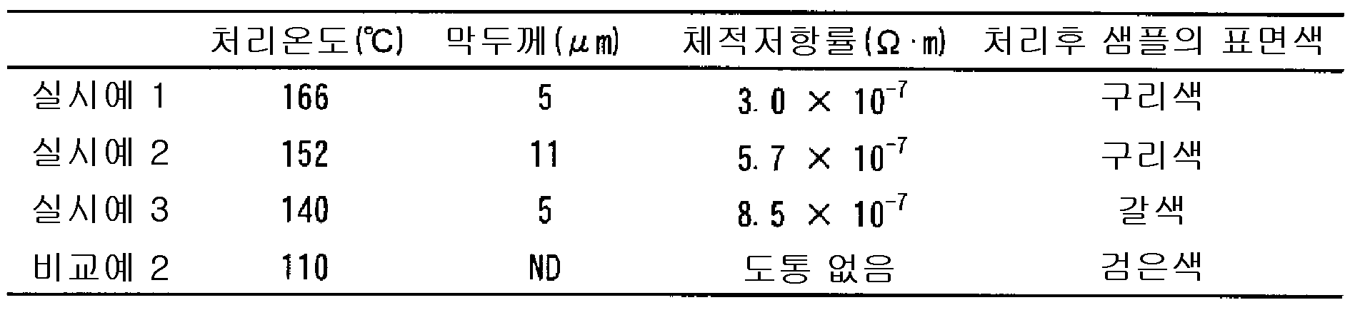
[실시예 4][Example 4]
분산제에 의해 금속 구리 나노 입자를 분산한 구리잉크(평균 입경 3~4nm(카탈로그치), Cu1T, ULVAC제) 4.7g을 실온에서 질소 가스를 내뿜어 분산매의 톨루엔을 증발 건조시킨 후, CuO 나노 입자(평균 입경 70 nm, 씨아이카세이) 25.7g과 γ-부티로락톤(와코쥰야쿠코교) 73g(고형분 27mass%)을 더해서 초음파 호모지나이저(US-600, 일본세이키제)에 의해 19.6kHz, 600W, 5분간 처리하고 원심분리기로 1500rpm, 4분간 처리하여 조립(粗粒)을 제외하고 구리잉크를 조제했다. 또한, 25℃에서의 동적 점도((주) Anton Paar, 점탄성 측정 장치 MCR301)는 10mPa·s, 평균 분산 입경(레이저 산란식 입도 분포 측정 장치, 벡크만코르타제 LS13320) 190nm, 최대 분산 입경 1,046nm였다.4.7 g of copper ink (average particle size of 3 to 4 nm (catalog value), Cu1T, manufactured by ULVAC) in which metal copper nanoparticles were dispersed by a dispersant was sprayed with nitrogen gas at room temperature to evaporate toluene of the dispersion medium, and then CuO nanoparticles (Manufactured by Nippon Seiki Co., Ltd.) was added with 25.7 g of a polyvinyl alcohol (average particle size: 70 nm, CI Cathay) and 73 g (solid content: 27 mass%) of gamma -butyrolactone (Wako Pure Chemical Industries, Treated for 5 minutes and treated with a centrifuge at 1500 rpm for 4 minutes to prepare a copper ink except for the coarse particles. The dynamic viscosity at 25 占 폚 (Anton Paar, Viscoelasticity Measuring Device MCR301) was 10 mPa 占 퐏, 190 nm of an average dispersed particle size (laser scattering type particle size distribution analyzer, Beckman Coulter LS13320) Respectively.
유리 프레파레트에 그 구리잉크를 갭 200㎛로 한 베이커 어플리케이터에 의해 도포하고, 실온 2시간 방치 후 100℃에 가열한 핫 플레이트 위에서 15분간 건조하여 구리계 입자 퇴적층을 가지는 샘플을 얻었다. 그 샘플을 실시예 1과 마찬가지로 포름산 가스로 처리했다. 그 구리잉크 도포 샘플은, 금속 광택을 가지는 구리색으로 변화하고, 4탐침법 저저항률계를 이용하여 측정한 표면 저항은 0.03Ω/□였다. 또한, 도포 부위외에의 구리의 석출은 보이지 않았다. FIB 가공 단면의 SEM 관찰로부터 측장한 막두께는 8㎛였다. 그 외, 평가 결과를 표 2에 나타냈다.The copper ink was coated on a glass pre-pallet by a baker applicator having a gap of 200 mu m, left at room temperature for 2 hours, and then dried on a hot plate heated at 100 DEG C for 15 minutes to obtain a sample having a copper-based particle deposit layer. The sample was treated with formic acid gas in the same manner as in Example 1. The copper ink applied sample was changed to a copper color having metallic luster, and the surface resistance measured with a 4-probe low resistivity meter was 0.03? / ?. In addition, precipitation of copper outside the application region was not observed. The film thickness measured from the SEM observation of the FIB working section was 8 μm. In addition, the evaluation results are shown in Table 2.
[실시예 5][Example 5]
(구리잉크의 조제)(Preparation of Copper Ink)
구리잉크는, CuO 나노 입자(평균 입경 70nm, 씨아이카세이) 27g을 폴리병에 칭량하고, 27mass%가 되도록 γ-부티로락톤(와코쥰야쿠코교) 73g을 더해서, 밀전 후 흔들어 섞은 후 초음파 호모지나이저(US-600, 일본세이키제)에 의해 19.6kHz, 600W, 5분간 처리하고, 원심분리기로 1500rpm, 4분간 처리하여 조립(粗粒)을 제외하고 구리잉크를 조제했다. 25℃에서의 동적 점도((주) 에·앤드·디, 소형 진동식 점토계 SV-10) 8mPa·s, 표면장력(전자동 표면장력계 CBVP-Z, 쿄와계면과학제) 45mN/m, 평균 분산 입경(레이저 산란식 입도 분포 측정 장치, 벡크만코르타제) 70nm, 최대 분산 입경 200nm이며, 잉크젯 인쇄에의 적용이 가능했다.Copper ink was prepared by weighing 27 g of CuO nanoparticles (average particle size 70 nm, Cai Kasei) into a poly bottle, and adding 73 g of gamma -butyrolactone (Wako Pure Yakako Kogyo Co., Ltd.) so as to be 27 mass%, shaking it after shaking, Treated at 19.6 kHz, 600 W for 5 minutes with a separator (US-600, Japan Seiki Co., Ltd.) and treated at 1500 rpm for 4 minutes using a centrifugal separator to prepare a copper ink except for the coarse particles. The dynamic viscosity at 25 캜 (SV-10, compact vibratory clay system SV-10) was found to be 8 mPa 揃 s, the surface tension (fully automatic surface tension meter CBVP-Z, manufactured by Kyowa Interface Science Co., Ltd.) The dispersion particle size (laser scattering type particle size distribution measurement apparatus, Beckman Coulter Co., Ltd.) was 70 nm and the maximum dispersion particle diameter was 200 nm, and it was applicable to inkjet printing.
(구리잉크 인쇄 샘플의 제작)(Production of Copper Ink Printing Sample)
유리 프레파레트 위에 그 잉크를 잉크젯 장치(MJP 프린터, 마이크로제트제)로 토출량 90ng/적(滴)으로 실시하고, 1cm×1cm의 면 위에 인쇄하여 구리잉크 인쇄 샘플을 얻었다. 구리잉크 인쇄물의 외형을 레이저 간섭형 표면 형상 측정 장치(MM3000, 료카시스템제)로 측정하여, 인쇄부와 유리 기판의 단차로부터 구리잉크 인쇄부의 막두께를 구한 바 1㎛였다.The ink was applied onto a glass pre-pallet at an ejection amount of 90 ng / drop (droplet) with an ink jet apparatus (MJP printer, micro jet) and printed on a surface of 1 cm x 1 cm to obtain a copper ink print sample. The appearance of the copper ink print was measured with a laser interference type surface shape measuring device (MM3000, manufactured by Ryoka System), and the film thickness of the copper ink print portion was calculated from the difference between the printing portion and the glass substrate.
(Platinum 입자 부여)(Platinum particle addition)
Platinum Powder(평균 입경: 0.14~0.45㎛(카탈로그치), Sigma-Aldrich Chemistry) 0.01g과 메틸 이소 부틸 케톤(와코쥰야쿠) 0.99g을 혼합하고, 초음파 세정기로 20분간 분산하여 침강하기 전에, 구리잉크 인쇄 샘플의 구리잉크 인쇄부에 한 방울 흘려, 구리잉크 인쇄부 전체로 편 후, 건조하여, Pt입자를 부여한 구리계 입자 퇴적층을 형성했다.0.01 g of platinum powder (average particle diameter: 0.14 to 0.45 탆 (catalog value), Sigma-Aldrich Chemistry) and 0.99 g of methyl isobutyl ketone (Wako Pure Chemical Industries) were mixed and dispersed for 20 minutes in an ultrasonic cleaner, One drop was poured into the copper ink printing portion of the ink print sample, and the entire copper ink printing portion was cut and dried to form a copper-based particle deposition layer to which Pt particles were added.
(포름산 가스 처리)(Formic acid gas treatment)
Pt입자를 부여한 구리계 입자 퇴적층의 포름산 가스 처리는, 실시예 1과 마찬가지로 실시하였다.Formic acid gas treatment of the copper-based particle deposited layer imparted with Pt particles was carried out in the same manner as in Example 1.
(특성 평가)(Characteristic evaluation)
체적 저항률은 4탐침법 저저항률계(로레스타 GP, 미츠비시카가쿠제)를 이용하여 측정한 표면 저항에 구리잉크 인쇄부의 막두께 1㎛를 곱하여 구했다.The volume resistivity was obtained by multiplying the surface resistance measured with a 4-probe low resistivity meter (Loresta GP, Mitsubishi Kagaku Co., Ltd.) by the film thickness of copper ink printed portion of 1 m.
본 샘플은 CuO 나노 입자의 검은색으로부터 환원의 진행에 수반하여, 구리색으로 변색한다. 이것을 눈으로 관찰하였다. 심부 환원성은, 유리 기판측으로부터 눈으로 인쇄부의 이면을 관찰하고, 구리색으로 변화했을 경우를 심부 환원성 있음으로 하였다. 도포 부위외에의 구리석출은 구리잉크가 인쇄되어 있지 않은 유리 기판 부분의 육안 관찰에 의해 확인했다. 유리 기판 위에 금속 구리가 석출했을 경우, 암록색에서 구리색으로 변색을 볼 수 있다.This sample is discolored to copper color as the reduction proceeds from the black color of the CuO nanoparticles. This was observed with eyes. As for the deep portion reducing property, the rear surface of the printed portion was visually observed from the glass substrate side, and when the color changed to copper color, the deep portion reducing property was determined. Copper precipitation outside the application region was confirmed by visual observation of the glass substrate portion where the copper ink was not printed. When metal copper is deposited on the glass substrate, the color change from dark green to copper color can be seen.
이상의 특성 평가 결과를 표 2에 나타냈다.The results of the above characteristics evaluation are shown in Table 2.
[실시예 6][Example 6]
Platinum Powder 대신에, Palladium Powder(평균 입경: 1.0~1.5㎛(카탈로그치), ChemPur제)를 이용한 것 이외에는 실시예 5와 마찬가지로 실시하였다. 평가 결과를 표 2에 나타냈다.The procedure of Example 5 was repeated except that Palladium Powder (average particle diameter: 1.0 to 1.5 占 퐉 (catalog value), manufactured by ChemPur) was used instead of Platinum Powder. The evaluation results are shown in Table 2.
[실시예 7][Example 7]
Platinum Powder 대신에, Silver Nanopowder(평균 입경<100nm(카탈로그치), Sigma-Aldrich Chemistry제)를 이용한 것 이외에는 실시예 5와 마찬가지로 실시하였다. 평가 결과를 표 2에 나타냈다.The procedure of Example 5 was repeated except that Silver Nanopowder (average particle diameter < 100 nm (catalog value), manufactured by Sigma-Aldrich Chemistry) was used instead of Platinum Powder. The evaluation results are shown in Table 2.
[실시예 8][Example 8]
Platinum Powder 대신에, Nickel Nanopowder(평균 입경<100nm(카탈로그치), Sigma-Aldrich Chemistry제)를 이용한 것 이외에는 실시예 5와 마찬가지로 실시하였다. 평가 결과를 표 2에 나타냈다.The procedure of Example 5 was repeated except that Nickel Nanopowder (average particle diameter <100 nm (catalog value), manufactured by Sigma-Aldrich Chemistry) was used instead of Platinum Powder. The evaluation results are shown in Table 2.
[실시예 9][Example 9]
Platinum Powder의 메틸 이소 부틸 케톤 분산액 대신에 클로로트리스(트리페닐 포스핀) 로듐(I)(와코쥰야쿠코교)의 테트라 히드로 푸란 용액을 이용한 것 이외에는 실시예 5와 마찬가지로 실시하였다. 평가 결과를 표 2에 나타냈다.The procedure of Example 5 was repeated except that a tetrahydrofuran solution of chlorotris (triphenylphosphine) rhodium (I) (Wako Pure Chemical Industries, Ltd.) was used instead of the methyl isobutyl ketone dispersion of platinum powder. The evaluation results are shown in Table 2.
[실시예 10][Example 10]
Platinum Powder의 메틸 이소 부틸 케톤 분산액 대신에 포름산 구리(II) 수화물(Sigma-Aldrich Chemistry제)의 γ-부티로락톤 포화 용액을 이용한 것 이외에는 실시예 5와 마찬가지로 실시하였다. 포름산 구리(II) 수화물은 질소 기류하에서 처리 온도까지 온도상승 할 때에 분해하여 금속 구리를 생성하고, 이 금속 구리가 촉매가 되어 구리잉크 도포부에만 금속 구리가 생성되었다고 생각했다. 그 외, 평가 결과를 표 2에 나타냈다.The procedure of Example 5 was repeated except that a saturated solution of γ-butyrolactone of copper (II) formate formate (manufactured by Sigma-Aldrich Chemistry) was used in place of the methyl isobutyl ketone dispersion of platinum powder. The copper (II) formate formate decomposed when heated to a treatment temperature under a nitrogen stream to produce metal copper, which was believed to be a catalyst and metal copper was produced only in the copper ink application portion. In addition, the evaluation results are shown in Table 2.
[실시예 11][Example 11]
구리잉크 인쇄막 표면에 금속 입자를 부여하는 대신에, 핫 와이어법 원자상 수소에 의해 환원하여 금속 구리으로 하고, 이것을 촉매 활성 금속 성분으로 한 구리계 입자 퇴적층에 대해서 포름산 환원을 실시했다. 이하에 상세한 내용을 적는다.Instead of applying metal particles to the surface of the copper ink print film, formic acid reduction was carried out on a copper-based particle deposited layer made of metallic copper as a catalytically active metal component by reduction with hot wire method atomic hydrogen. Details are given below.
(구리잉크 인쇄 샘플 제작)(Copper ink printing sample production)
실시예 5와 마찬가지로 구리잉크 인쇄 샘플을 제작했다.A copper ink print sample was produced in the same manner as in Example 5.
(핫 와이어법 원자상 수소 처리)(Hot wire method atomic hydrogen treatment)
핫 와이어법 원자상 수소 처리는, 수소를 도입한 핫 와이어 CVD 장치(유니버셜시스템즈제)를 이용하여, 수소 유량 20sccm, 조내(槽內) 압력 0.4Pa, 텅스텐 와이어 투입 전력 520W, 텅스텐 와이어 온도 1560℃(방사 온도계 측정), 처리 시간 10분의 조건으로 처리했다. 핫 와이어법 원자상 수소 처리 후의 샘플 표면은 암갈색, 유리 기판측에서 관찰한 샘플 이면은 검은색이며, 표면만이 환원되었다. 표면 저항은 657Ω/□였다.The hot wire method The hydrogen treatment was carried out by using a hot wire CVD apparatus (manufactured by Universal Systems Corporation) into which hydrogen was introduced at a hydrogen flow rate of 20 sccm, a pressure in the tank of 0.4 Pa, a tungsten wire input power of 520 W, (Measurement of radiation thermometer) and a treatment time of 10 minutes. Hot wire method The surface of the sample after the atomic hydrogen treatment was dark brown and the surface of the sample observed on the glass substrate side was black, and only the surface was reduced. The surface resistance was 657? / ?.
(포름산 가스 처리)(Formic acid gas treatment)
핫 와이어법 원자상 수소 처리 후의 구리잉크 인쇄 샘플의 구리계 입자 퇴적층을 실시예 6과 마찬가지로 포름산 가스 처리, 평가하였다. 표면색은 윤기없는 구리색, 유리 기판면측은 금속 광택이 있는 구리색이며, 체적 저항률은 8.0×10⁻⁸Ω·m였다. 그 외, 평가 결과를 표 2에 나타냈다.The copper-based particle deposited layer of the copper ink printed sample after the hot wire method atomic hydrogen treatment was evaluated by treating with formic acid gas in the same manner as in Example 6. The surface color was copper-free and the glass substrate side was copper-colored with metallic luster. The volume resistivity was 8.0 × 10 -8 Ω · m. In addition, the evaluation results are shown in Table 2.
[실시예 12][Example 12]
실시예 1에서 사용한 동박 부착 기판을 산성 팔라듐 시더 용액(히타치카세이코교(주)제, 상품명: PD301 250g/L, 히타치카세이코교(주)제, 상품명: HS202B 30mL/L)에 실온에서 10분간 침지 후, 1M 황산 수용액으로 1분간 처리, 초순수에 담그어 세정, 실온에서 건조하여 기판 표면에 팔라듐 입자를 파종한 기판을 얻었다.The substrate with the copper foil used in Example 1 was dissolved in 10 ml of an acidic palladium cysteine solution (trade name: PD301 250 g / L, Hitachi Kasei Corporation, trade name: HS202B 30 mL / After minute immersion, the substrate was treated with a 1 M sulfuric acid aqueous solution for 1 minute, immersed in ultrapure water, washed, and dried at room temperature to obtain a substrate on which palladium particles were sown on the substrate surface.
그 팔라듐 입자 파종 기판에 실시예 5의 구리잉크를 갭 100㎛로 조정한 베이커 어플리케이터에 의해 도포했다. 그 후, 100℃로 가열한 핫 플레이트 위에 놓고 15분간 건조하여 구리계 입자 퇴적층을 형성하여 구리잉크 도포 기판을 얻었다.The copper ink of Example 5 was applied to the palladium particle seeding substrate by a Baker applicator adjusted to have a gap of 100 占 퐉. Thereafter, the substrate was placed on a hot plate heated to 100 占 폚 and dried for 15 minutes to form a copper-based particle deposition layer to obtain a copper ink-coated substrate.
그 구리잉크 도포 기판을 실시예 5와 마찬가지로 포름산 가스 처리, 평가하였다. 그 결과, 구리잉크 도포 기판 이외의 반응 용기에는 구리의 석출은 없었다. 도체층의 표면 저항률은 0.019Ω/□였다. 그 외, 평가 결과를 표 2에 나타냈다.The copper ink application substrate was subjected to formic acid gas treatment in the same manner as in Example 5. As a result, there was no precipitation of copper in the reaction vessel other than the copper ink application substrate. The surface resistivity of the conductor layer was 0.019? / ?. In addition, the evaluation results are shown in Table 2.
[비교예 3][Comparative Example 3]
실시예 5의 구리잉크 인쇄 기판에 플라티나 입자를 부착하지 않고, 실시예 5와 마찬가지로 포름산 가스 처리, 평가하였다. 평가 결과를 표 2에 나타냈다.The platinum particles were not adhered to the copper ink print substrate of Example 5, and treated with formic acid gas in the same manner as in Example 5, and evaluated. The evaluation results are shown in Table 2.
[표 2][Table 2]
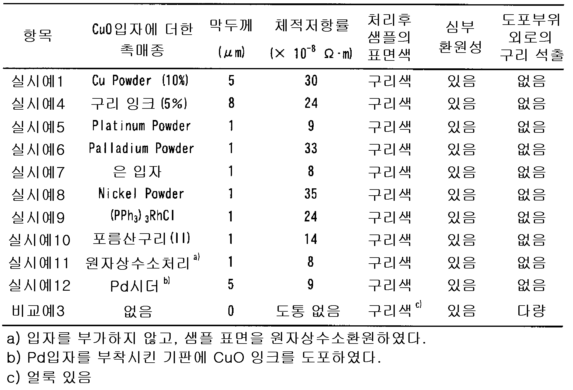
[비교예 4][Comparative Example 4]
포름산 구리수화물(Sigma-Aldrich Chemistry제)의 5mass% 수용액을, 동박을 에칭한 동박 부착 에폭시 기판(E-679F, 히타치카세이코교제) 위에 도포하고, 110℃의 핫 플레이트 위에서 건조하여 기판 위에 포름산 구리수화물이 결정립으로서 부착한 기판을 얻었다. 그 기판을 160℃로 가열한 핫 플레이트 위에 놓고, 거꾸로 한 깔때기를 씌워, 깔때기의 유리관 쪽으로부터 질소를 흘려 질소 분위기로 하여 20분간 처리했다.A 5 mass% aqueous solution of copper hydrate formic acid (Sigma-Aldrich Chemistry) was applied on a copper foil-coated epoxy substrate (E-679F, Hitachi Chemical Co., Ltd.) etched with copper foil and dried on a hot plate at 110 占 폚, Whereby a substrate having hydrates attached as crystal grains was obtained. The substrate was placed on a hot plate heated to 160 ° C, covered with an inverted funnel, treated with nitrogen for 20 minutes by flowing nitrogen through the glass tube of the funnel.
포름산 구리 도포부는 구리색으로 변화하고, 포름산 구리 도포부의 주위의 기판도 구리색으로 변색했다.The copper formate coated portion changed to a copper color, and the substrate around the copper formate coated portion also changed to a copper color.
실시예 1과 마찬가지로 도체층을 평가하고, 처리 후의 포름산 구리 도포부의 FIB 가공 단면의 SEM상(像)으로부터 구한 막두께는 6㎛, 표면 저항 측정으로부터 구한 체적 저항률은 4.2×10⁻⁶Ω·m였다.The conductor layer was evaluated in the same manner as in Example 1, and the film thickness obtained from the SEM image of the FIB-processed cross section of the copper formate coated portion after the treatment was 6 탆 and the volume resistivity determined from the surface resistance measurement was 4.2 10 -6 Ω · m Respectively.
이상과 같이, 포름산 구리는 열분해하여 금속 구리를 생성하였다. 또한, 포름산 구리는 승화성을 가지며, 도포부 주위의 기판 위에도 금속 구리가 석출했다.As described above, copper formate was pyrolyzed to produce metallic copper. Further, copper formate had sublimation properties, and metal copper also precipitated on the substrate around the coated portion.
[비교예 5][Comparative Example 5]
처리 가스로서 포름산 대신에 이소프로판올을 이용한 것 이외에는 실시예 2와 마찬가지로 실시하여, 처리 샘플을 얻었다. 표면 저항을 4탐침법 저저항률계(로레스타 GP, 미츠비시 화학제)에 의해 측정했지만, 측정 한계 이상, 즉 도통은 보이지 않았다. 표면색을 눈으로 관찰했지만, 처리전과 같은 검은색이며 이소프로판올 가스 처리 전후에서 변화는 보이지 않았다. 그 외, 평가 결과를 표 3에 나타냈다.A treated sample was obtained in the same manner as in Example 2 except that isopropanol was used instead of formic acid as the treatment gas. The surface resistance was measured by a 4-probe low resistivity meter (Loresta GP, Mitsubishi Chemical), but the measurement limit or more, that is, conduction was not observed. The surface color was observed with the eye, but it was black as before the treatment and no change was observed before or after the isopropanol gas treatment. In addition, the evaluation results are shown in Table 3.
[비교예 6][Comparative Example 6]
처리 가스로서 포름산 대신에 에틸렌글리콜을 이용한 것 이외에는 실시예 2와 마찬가지로 실시하여, 처리 샘플을 얻었다. 비교예 5와 마찬가지로 평가한 바, 도통은 보이지 않고, 표면색은 검은색인 채 변화는 보이지 않았다. 그 외, 평가 결과를 표 3에 나타냈다.A treated sample was obtained in the same manner as in Example 2 except that ethylene glycol was used instead of formic acid as the treatment gas. Evaluation was made in the same manner as in Comparative Example 5, no conduction was observed, and the surface color was black, and no change was observed. In addition, the evaluation results are shown in Table 3.
[비교예 7][Comparative Example 7]
처리 가스로서 포름산 대신에 아세트산을 이용한 것 이외에는 실시예 2와 마찬가지로 실시하여, 처리 샘플을 얻었다. 비교예 5와 마찬가지로 평가한 바, 도통은 보이지 않고, 표면색은 검은색인 채 변화는 보이지 않았다. 그 외, 평가 결과를 표 3에 나타냈다.A treated sample was obtained in the same manner as in Example 2 except that acetic acid was used instead of formic acid as the treatment gas. Evaluation was made in the same manner as in Comparative Example 5, no conduction was observed, and the surface color was black, and no change was observed. In addition, the evaluation results are shown in Table 3.
[비교예 8][Comparative Example 8]
처리 가스로서 포름산 대신에 아세트산과 에틸렌글리콜의 혼합물을 이용한 것 이외에는 실시예 2와 마찬가지로 실시하여, 처리 샘플을 얻었다. 비교예 5와 마찬가지로 평가한 바, 도통은 보이지 않고, 표면색은 검은색인 채 변화는 보이지 않았다. 그 외, 평가 결과를 표 3에 나타냈다.A treated sample was obtained in the same manner as in Example 2 except that a mixture of acetic acid and ethylene glycol was used in place of formic acid as the treatment gas. Evaluation was made in the same manner as in Comparative Example 5, no conduction was observed, and the surface color was black, and no change was observed. In addition, the evaluation results are shown in Table 3.
[비교예 9][Comparative Example 9]
처리 가스로서 포름산 대신에 아세트알데히드를 이용한 것 이외에는 실시예 2와 마찬가지로 실시하여, 처리 샘플을 얻었다. 비교예 5와 마찬가지로 평가한 바, 도통은 보이지 않고, 표면색은 검은색인 채 변화는 보이지 않았다. 그 외, 평가 결과를 표 3에 나타냈다.A treated sample was obtained in the same manner as in Example 2 except that acetaldehyde was used instead of formic acid as the treatment gas. Evaluation was made in the same manner as in Comparative Example 5, no conduction was observed, and the surface color was black, and no change was observed. In addition, the evaluation results are shown in Table 3.
[비교예 10][Comparative Example 10]
처리 가스로서 포름산 대신에 아세산과 아세트알데히드의 혼합물을 이용한 것 이외에는 실시예 2와 마찬가지로 실시하여, 처리 샘플을 얻었다. 비교예 6과 마찬가지로 평가한 바, 도통은 보이지 않고, 표면색은 검은색인 채 변화는 보이지 않았다.A treated sample was obtained in the same manner as in Example 2 except that a mixture of acetic acid and acetaldehyde was used in place of formic acid as a treatment gas. Evaluation was made in the same manner as in Comparative Example 6, no conduction was observed, and the surface color was black, and no change was observed.
그 외, 평가 결과를 표 3에 나타냈다.In addition, the evaluation results are shown in Table 3.
[표 3][Table 3]

[실시예 13][Example 13]
구리잉크 심부의 환원성을 평가하기 위해, 잉크를 두껍게 담아 평가를 실시했다.In order to evaluate the reducibility of the copper ink core part, evaluation was carried out with thick ink.
구리잉크는, CuO 나노 입자 40.5g과 표면 자연 산화 Cu 나노 입자 4.5g(CuO 입자:Cu입자=90:10)을 폴리병에 칭량하고, 고형분 45mass%가 되도록 γ-부티로락톤 5g을 더해서, 밀전 후 흔들어 섞은 후 초음파 세정기(B5510J-MTH, Branson제)에 의해 60분간 처리하여 페이스트상(狀)의 구리잉크를 조제했다.In the copper ink, 40.5 g of CuO nanoparticles and 4.5 g of surface naturally oxidized Cu nanoparticles (CuO particles: Cu particles = 90: 10) were weighed in a poly bottle and 5 g of gamma -butyrolactone was added thereto so as to have a solid content of 45 mass% After shaking, the mixture was shaken and treated with an ultrasonic cleaner (B5510J-MTH, manufactured by Branson) for 60 minutes to prepare a paste-like copper ink.
이 페이스트상의 구리잉크를 캐필러리 시린지로부터 압출하여 유리 프레파레트 위에 두께 0.8mm의 언덕모양으로 부착, 건조시켜 구리계 입자 퇴적층을 형성한 후, 실시예 1과 마찬가지로 포름산 가스로 처리했다.This paste-type copper ink was extruded from a capillary syringe and attached on a glass pre-pallet in the form of a hill having a thickness of 0.8 mm and dried to form a copper-based particle deposit layer, and then treated with formic acid gas in the same manner as in Example 1.
유리 기판측에서의 육안 관찰에 있어서 모두 구리색으로 변화하고 있어, 심부 환원성이 있다고 판단했다. 도 5에 그 모습을 관찰한 도면 대용 사진을 나타냈다. 도 5(B)가 유리 기판측으로부터 관찰한 것이다.All of them were changed to copper color in the visual observation on the glass substrate side, and it was judged that there was deep reducing ability. Fig. 5 shows a photograph for the observation of its appearance. Fig. 5 (B) is observed from the glass substrate side.
[비교예 11][Comparative Example 11]
비교예 1과 마찬가지로 하여 조제한 구리잉크를 베이커 어플리케이터에 의해 유리 프레파레트에 도포하고, 100℃로 가열한 핫 플레이트 위에 두고 15분간 건조하여 구리계 입자 퇴적층을 형성한 구리잉크 도포 샘플을 얻었다. 이 구리잉크 도포 샘플을 실시예 1의 포름산 가스 처리용의 반응 용기에 세트하고, 포름산 가스를 포함하는 질소 가스를 도입해서 실온부터 160℃로 가열하여, 160℃에 달한 후 60분간 처리했다. 그 결과, 구리잉크 도포 샘플이 얼룩이 있는 구리색으로 변화했지만, 주변이나 반응 용기의 내벽에도 다량의 구리가 석출됐다.The copper ink prepared in the same manner as in Comparative Example 1 was applied to a glass pre-palette by a baker applicator and placed on a hot plate heated to 100 占 폚 for 15 minutes to obtain a copper ink coated sample having a copper particle deposited layer. This copper ink application sample was set in a reaction vessel for the treatment of formic acid gas in Example 1, and nitrogen gas containing formic acid gas was introduced, heated from room temperature to 160 占 폚, reached 160 占 폚 and treated for 60 minutes. As a result, although the copper ink application sample was changed to a speckled copper color, a large amount of copper precipitated around the inner wall of the reaction vessel.
[실시예 14][Example 14]
(구리잉크 조제)(Copper ink preparation)
구리잉크는 실시예 5와 마찬가지로 조제했다.The copper ink was prepared in the same manner as in Example 5.
(기판 제작)(Substrate production)
비스페놀 A 노볼락 에폭시 수지(N865, 다이닛폰잉크카가쿠코교제) 10g, 경화제(LA3018, 다이닛폰잉크카가쿠코교제) 7.26g, 2-에틸-4-메틸이미다졸(와코쥰야쿠코교제) 0.017g, 표면장력 조정제(307, 빅케미제) 0.022g을 2-아세톡시-1-메톡시 프로판(와코쥰야쿠코교제) 24.2g에 용해하여 수지 용액을 얻었다. 탁상형 표면 처리 장치(PL16-110A, 센특수광원제)로 UV/03 처리한 유리 프레파레트 위에, 그 수지 용액을 1500rpm, 60sec의 조건으로 스핀 코트하고, 100℃의 핫 플레이트 위에서 10분 건조 후, 180℃의 핫 플레이트 위에서 30분 경화하여 수지 도포 기판을 제작했다.10 g of bisphenol A novolak epoxy resin (N865, manufactured by Dainippon Ink and Chemicals, Incorporated), 7.26 g of a curing agent (LA3018, manufactured by Dainippon Ink and Chemicals, Incorporated) And 0.022 g of a surface tension adjuster (307, Big Chemie) were dissolved in 24.2 g of 2-acetoxy-1-methoxypropane (Wako Pure Chemical Industries, Ltd.) to obtain a resin solution. The resin solution was spin-coated on a glass pre-pallet treated with UV / 0 3 with a tabletop type surface treatment apparatus (PL16-110A, manufactured by Sen special light source) under the conditions of 1500 rpm for 60 seconds and dried on a hot plate at 100 ° C. for 10 minutes And then cured on a hot plate at 180 ° C for 30 minutes to prepare a resin-coated substrate.
(구리잉크 인쇄 샘플 제작)(Copper ink printing sample production)
그 수지 도포 기판 위에, 실시예 6과 마찬가지로 하여 구리잉크를 잉크젯 인쇄해서 구리잉크 인쇄 샘플을 얻었다.On the resin-coated substrate, a copper ink was printed by ink jet printing in the same manner as in Example 6 to obtain a copper ink printed sample.
(핫 와이어법 원자상 수소 처리)(Hot wire method atomic hydrogen treatment)
실시예 11과 마찬가지로 구리잉크 인쇄 샘플을 핫 와이어법 원자상 수소 처리하여 구리계 입자 퇴적층을 형성했다. 핫 와이어법 원자상 수소 처리 후의 샘플 표면은 암갈색, 유리 기판측에서 관찰한 샘플 이면은 검은색이었다. 표면 저항 측정에 있어서 측정 한계 이상의 저항으로 도통은 보이지 않았다.As in Example 11, a copper ink printed sample was subjected to a hot wire atomic hydrogen treatment to form a copper-based particle deposition layer. Hot wire method The surface of the sample after the raw material hydrogen treatment was dark brown and the sample behind the glass substrate was black. In the surface resistance measurement, no conduction was observed with a resistance higher than the measurement limit.
(포름산 가스 처리)(Formic acid gas treatment)
핫 와이어법 원자상 수소 처리한 구리잉크 인쇄 샘플의 포름산 가스 처리는, 실시예 1과 마찬가지로 실시하였다. 처리 후의 체적 저항률은 7.8×10⁻⁸Ω·m였다.The formic acid gas treatment of the copper ink print sample subjected to the hot wire method and the hydrogen treatment was conducted in the same manner as in Example 1. The volume resistivity after the treatment was 7.8 × 10 -8 Ω · m.
(기판 밀착성 측정)(Measurement of substrate adhesion)
포름산 가스 처리 후의 구리잉크 인쇄층의 기판 밀착성은 SAICAS에 의해 박리 강도를 측정했다. 평균 박리 강도는 0.32kN/m였다.The substrate adhesion of the copper ink printed layer after the treatment with formic acid was measured for peel strength by SAICAS. The average peel strength was 0.32 kN / m.
포름산 가스 처리한 구리잉크 인쇄층의 기판 밀착성은 비교예 13과 비교하여 2.3배가 되어, 밀착력이 향상되었다. 도 3에 보여지는 기판에 따른 치밀층의 존재에 의해 접착 면적이 증가하여 밀착력이 향상됐다고 생각한다.The substrate adhesion of the copper ink printed layer treated with formic acid was 2.3 times that of Comparative Example 13, and the adhesion was improved. The adhesion area is increased by the presence of the dense layer according to the substrate shown in FIG. 3, and the adhesion is improved.
[비교예 12][Comparative Example 12]
(구리잉크 인쇄 샘플 제작)(Copper ink printing sample production)
실시예 14와 마찬가지로 구리잉크 인쇄 샘플을 제작했다.A copper ink print sample was produced in the same manner as in Example 14.
(핫 와이어법 원자상 수소 처리)(Hot wire method atomic hydrogen treatment)
핫 와이어법 원자상 수소 처리는, 수소를 도입한 핫 와이어 원자상 수소 처리 장치를 이용하여, 수소 유량 70sccm, 수조내 압력 0.4Pa, 텅스텐 와이어 투입 전력 1030W, 텅스텐 와이어 온도 1800℃(방사 온도계 측정), 처리 시간 40분의 조건으로 처리했다. 처리 후의 샘플 표면은 구리색, 유리 기판측으로부터 관찰한 샘플 이면은 암갈색이며, 구리잉크 막두께 1.7㎛의 이면까지 환원되었다. 체적 저항률은 1.7×10⁻⁶Ω·m였다.Hot wire method The hydrogen treatment was carried out by using a hot wire atomic hydrogen processor with hydrogen introduced at a hydrogen flow rate of 70 sccm, a pressure in a water bath of 0.4 Pa, a tungsten wire input power of 1030 W, a tungsten wire temperature of 1800 캜 (radiation thermometer) , And the treatment time was 40 minutes. The surface of the sample after the treatment was copper-colored, and the backside of the sample observed from the glass substrate side was dark brown, and was reduced to the back surface of the copper ink film thickness of 1.7 탆. The volume resistivity was 1.7 × 10 -6 Ω · m.
(기판 밀착성 측정)(Measurement of substrate adhesion)
실시예 14와 같게 측정한 평균 박리 강도는 0.14kN/m였다.The average peel strength measured in the same manner as in Example 14 was 0.14 kN / m.
[실시예 15][Example 15]
포름산 가스로 바꾸어 포름알데히드를 이용한 도체화 처리를 실시했다. 이하에 상세한 내용을 적는다.Conductivization treatment with formaldehyde was carried out by replacing with formic acid gas. Details are given below.
실시예 11과 마찬가지로 하여, 구리잉크 인쇄막 표면을 핫 와이어법 원자상 수소에 의해 환원하여 구리잉크 인쇄조표면을 금속 구리로 한 샘플을 제작했다(체적 저항률 6.0×10⁻⁶Ω·m).The surface of the copper ink print film was reduced by hot wire method in the form of hydrogen in the same manner as in Example 11 to produce a sample having a surface of copper ink printing plate made of metal copper (volume resistivity: 6.0 × 10 -6 Ω · m).
100ml 가지형 플라스크에 파라포름알데히드를 10g 넣고 문질러 비벼서 삼방 코크를 붙여, 위의 유리관으로부터 20cm의 주사바늘을 찔러넣어 파라피룸으로 유리관과의 틈새를 밀폐하고, 주사바늘로부터 질소를 흘리면서 가지형 플라스크를 160℃의 오일배스에 담그어 가열하여, 삼방 코크의 측관으로부터 포름알데히드를 포함한 질소 가스를 얻었다. 그 샘플을 오일배스에서 가열한 평저의 세퍼러블 플라스크의 바닥에 바다모래를 깐 후에 세트하였다. 이 샘플 표면에 크로멜 알루멜 열전쌍를 세트하여 샘플 온도를 측정했다. 이 샘플을 세트한 세퍼러블 플라스크에 포름알데히드를 포함하는 질소를 흘리면서 197℃의 오일배스에서 가열하고, 샘플의 온도 160℃에서, 60분간 처리했다. 처리 후, 포름산 가스의 발생 장치를 떼어 내고, 질소를 흘리면서 세퍼러블 플라스크를 방랭하고, 샘플이 50도 이하가 된 후, 샘플을 공기중에 꺼냈다. 그 결과, 샘플의 표면색은 암갈색에서 갈색으로 변색하고, 유리 기판측의 색은 검은색에서 적구리색으로 변색했다. 체적 저항률은 5.4×10⁻⁷Ω·m였다.10 g of paraformaldehyde was added to a 100 ml eggplant-shaped flask, rubbed with a three-way cock, and a 20 cm needle was pierced from the upper glass tube to seal the gap between the glass tube and the glass tube. While flowing nitrogen from the injection needle, Immersed in an oil bath at 160 캜 and heated to obtain nitrogen gas containing formaldehyde from the side pipes of the three-way cock. The sample was set on the bottom of a flat, separable flask heated in an oil bath and sandwiched with sea sand. A chromel-alumel thermocouple was set on the surface of the sample to measure the sample temperature. The separable flask in which the sample was set was heated in an oil bath at 197 DEG C while flowing nitrogen containing formaldehyde, and treated at a sample temperature of 160 DEG C for 60 minutes. After the treatment, the apparatus for generating formic acid gas was removed, and the separable flask was allowed to cool while flowing nitrogen. After the sample became 50 degrees or less, the sample was taken out into the air. As a result, the surface color of the sample discolored from dark brown to brown, and the color on the glass substrate side changed from black to red copper color. The volume resistivity was 5.4 x 10 < " 7 >
[실시예 16][Example 16]
실시예 1과 마찬가지로 제작한 구리잉크 도포 샘플을, 실시예 15와 마찬가지로 포름알데히드로 처리했다. 그 결과, 구리잉크 표면은 검은색에서 윤기없는 구리색으로 변화하고, 유리 기판측도 검은색에서 윤기없는 구리색으로 변화했다. 처리전에 도통이 없었던 구리잉크는 처리 후에 체적 저항률 9.0×10⁻⁷Ω·m로 도통이 얻어졌다.The copper ink application sample prepared in the same manner as in Example 1 was treated with formaldehyde in the same manner as in Example 15. As a result, the surface of the copper ink changed from black to a non-glossy copper color, and the glass substrate side also changed from black to non-glossy copper color. The copper ink, which had no conduction before the treatment, had a volume resistivity of 9.0 x 10 <" 7 >
실시예 15 및 실시예 16으로부터 포름알데히드 가스와 함께 가열하는 것에 의해서도 구리잉크가 도체화하였다. 각각, 포름산 가스로 처리한 실시예 1, 실시예 11과 비교하면, 1시간 처리했음에도 불구하고, 처리 후의 구리잉크의 색조가 약간 어둡고, 체적 저항률도 높아져 있어, 포름알데히드에서는 포름산 가스 보다 약간 효과가 낮았다.From Example 15 and Example 16, the copper ink was also made conductive by heating with formaldehyde gas. Compared with Example 1 and Example 11 treated with formic acid gas, the color tone of the copper ink after treatment was slightly darker and the volume resistivity was higher, even though the treatment was carried out for 1 hour. In formaldehyde, Low.
12 촉매 활성 금속 성분
13 구리 산화물 성분
14 촉매 활성 성분을 포함해서 이루어지는 입자
15 구리 산화물 성분을 포함해서 이루어지는 입자
16, 19 기판
17, 21, 22 촉매 활성 금속 성분으로 이루어지는 입자층
18, 20 구리 산화물 성분으로 이루어지는 입자 퇴적층
23 촉매 활성 금속 성분의 막
24 구리 산화물 성분으로 이루어지는 입자 퇴적층12 Catalyst active metal component
13 Copper oxide component
14 Particles comprising a catalytically active component
15 Particles comprising a copper oxide component
16, 19 substrate
17, 21, 22 A particle layer made of a catalytically active metal component
18, 20 Particle deposition layer made of copper oxide
23 Membrane of catalytically active metal components
24 Particle deposition layer made of copper oxide component
Claims (4)
상기 천이 금속, 합금, 또는 천이 금속 착체가, 각각, Cu, Pd, Pt, Ni, Ag, Au, 및 Rh로 이루어지는 군으로부터 선택되는 금속, 또는 그 금속을 포함하는 합금, 또는 그 금속 원소를 포함하는 착체이고,
상기 금속, 그 금속을 포함하는 합금, 또는 그 금속 원소를 포함하는 착체가 입자상이고, 상기 입자의 최대 분산 입경이 2㎛ 이하가 되도록 분산하고 있으며, 그 입자의 표면적이 구리 산화물을 포함하는 입자의 중량 1g에 대하여 0.4m2 이상이 되도록 포함하는 것을 특징으로 하는 액상 조성물.A transition metal complex comprising copper oxide, a transition metal or alloy of a metal, or a transition metal element, and a solvent having a vapor pressure at 25 캜 of less than 1.34 x 10 3 Pa, wherein the copper oxide and the transition metal, Or transition metal complexes are present in the form of particles and the average dispersed particle size of the particles is not more than 500 nm and the maximum dispersed particle diameter is not more than 2 탆 and the content of the copper oxide is less than or equal to the copper oxide, Wherein the liquid composition is 1 to 80 parts by volume based on 100 parts by volume of the total amount of the metal, the alloy, the transition metal complex containing the transition metal element,
Wherein the transition metal, alloy or transition metal complex comprises a metal selected from the group consisting of Cu, Pd, Pt, Ni, Ag, Au, and Rh, or an alloy containing the metal or a metal element thereof Lt; / RTI >
Wherein the metal, the alloy containing the metal, or the complex containing the metal element is in a particulate state and the maximum dispersed particle size of the particles is 2 mu m or less, and the surface area of the particles is Wherein the liquid composition contains 0.4 m 2 or more per 1 g of the liquid.
상기 구리 산화물, 및 상기 금속상의 천이 금속 혹은 합금, 또는 천이 금속 원소를 포함하는 천이 금속 착체로서, 코어부가 그 천이 금속 또는 합금이며, 쉘부가 그 구리 산화물인 코어-쉘 구조를 가지는 입자를 포함하는 것을 특징으로 하는 액상 조성물.The method according to claim 1,
A transition metal complex comprising the copper oxide and the transition metal or alloy or transition metal element on the metal, the transition metal complex including particles having a core-shell structure in which the core portion is the transition metal or alloy thereof and the shell portion is the copper oxide ≪ / RTI >
상기 금속 원소를 포함하는 착체가 상기 용제의 용액을 이루고 있으며, 그 착체의 함유량이 그 착체 중의 금속 원자의 중량이 구리 산화물을 포함하는 입자의 중량을 100으로 했을 때에 1~100인 것을 특징으로 하는 액상 조성물.The method according to claim 1,
Wherein the complex containing the metal element constitutes a solution of the solvent and the content of the complex is 1 to 100 when the weight of the metal atom in the complex is 100 and the weight of the particles containing the copper oxide is 100 Liquid composition.
25℃에서의 동적 점도가 100mPa·s 이하인 것을 특징으로 하는 액상 조성물.4. The method according to any one of claims 1 to 3,
And a dynamic viscosity at 25 占 폚 of 100 mPa 占 퐏 or less.
Applications Claiming Priority (3)
| Application Number | Priority Date | Filing Date | Title |
|---|---|---|---|
| JP2009215003 | 2009-09-16 | ||
| JPJP-P-2009-215003 | 2009-09-16 | ||
| PCT/JP2010/065698 WO2011034016A1 (en) | 2009-09-16 | 2010-09-13 | Copper metal film, method for producing same, copper metal pattern, conductive wiring line using the copper metal pattern, copper metal bump, heat conduction path, bonding material, and liquid composition |
Related Parent Applications (1)
| Application Number | Title | Priority Date | Filing Date |
|---|---|---|---|
| KR1020127008376A Division KR20120093188A (en) | 2009-09-16 | 2010-09-13 | Copper metal film, method for producing same, copper metal pattern, conductive wiring line using the copper metal pattern, copper metal bump, heat conduction path, bondig material, and liquid composition |
Publications (2)
| Publication Number | Publication Date |
|---|---|
| KR20160044062A true KR20160044062A (en) | 2016-04-22 |
| KR101697055B1 KR101697055B1 (en) | 2017-01-16 |
Family
ID=43758620
Family Applications (2)
| Application Number | Title | Priority Date | Filing Date |
|---|---|---|---|
| KR1020127008376A KR20120093188A (en) | 2009-09-16 | 2010-09-13 | Copper metal film, method for producing same, copper metal pattern, conductive wiring line using the copper metal pattern, copper metal bump, heat conduction path, bondig material, and liquid composition |
| KR1020167009435A KR101697055B1 (en) | 2009-09-16 | 2010-09-13 | Copper metal film, method for producing same, copper metal pattern, conductive wiring line using the copper metal pattern, copper metal bump, heat conduction path, bondig material, and liquid composition |
Family Applications Before (1)
| Application Number | Title | Priority Date | Filing Date |
|---|---|---|---|
| KR1020127008376A KR20120093188A (en) | 2009-09-16 | 2010-09-13 | Copper metal film, method for producing same, copper metal pattern, conductive wiring line using the copper metal pattern, copper metal bump, heat conduction path, bondig material, and liquid composition |
Country Status (9)
| Country | Link |
|---|---|
| US (1) | US9457406B2 (en) |
| EP (1) | EP2479314B1 (en) |
| JP (1) | JP5747821B2 (en) |
| KR (2) | KR20120093188A (en) |
| CN (2) | CN104475758B (en) |
| MY (1) | MY169953A (en) |
| SG (1) | SG10201405419XA (en) |
| TW (1) | TWI494471B (en) |
| WO (1) | WO2011034016A1 (en) |
Families Citing this family (25)
| Publication number | Priority date | Publication date | Assignee | Title |
|---|---|---|---|---|
| KR100922810B1 (en) * | 2007-12-11 | 2009-10-21 | 주식회사 잉크테크 | A method for fabricating blackened conductive patterns |
| US8758638B2 (en) * | 2011-05-10 | 2014-06-24 | Applied Materials, Inc. | Copper oxide removal techniques |
| WO2013018777A1 (en) | 2011-08-03 | 2013-02-07 | 日立化成工業株式会社 | Composition set, electroconductive substrate and manufacturing method thereof, and electroconductive binding material composition |
| DE102011080620B4 (en) * | 2011-08-08 | 2014-06-05 | Siemens Aktiengesellschaft | Method for coating an insulation component and insulation component, and electrically conductive heating cable |
| TW201339279A (en) * | 2011-11-24 | 2013-10-01 | Showa Denko Kk | Conductive-pattern formation method and composition for forming conductive pattern via light exposure or microwave heating |
| KR101353149B1 (en) * | 2011-12-27 | 2014-01-27 | 삼성전기주식회사 | Manufacturing mehtod for copper powder |
| JP2013175560A (en) * | 2012-02-24 | 2013-09-05 | Hitachi Chemical Co Ltd | Metal copper film obtained by forming into conductor at 140°c or less, metal copper pattern, and their manufacturing method |
| JP2013206722A (en) * | 2012-03-28 | 2013-10-07 | Fujifilm Corp | Liquid composition, metal copper film, conductor wiring, and method for manufacturing metal copper film |
| KR101525652B1 (en) * | 2012-05-04 | 2015-06-03 | 삼성전기주식회사 | Conductive resin composition, multi layer ceramic capacitor having the same and manufacturing method thereof |
| JP2014067617A (en) * | 2012-09-26 | 2014-04-17 | Fujifilm Corp | Method for producing conductive film and conductive film-forming composition |
| US9234112B2 (en) * | 2013-06-05 | 2016-01-12 | Korea Institute Of Machinery & Materials | Metal precursor powder, method of manufacturing conductive metal layer or pattern, and device including the same |
| KR101582637B1 (en) * | 2013-07-29 | 2016-01-07 | 전북대학교산학협력단 | Fabrication of CuO Nanoparticles and Thereof Ink and Microwave-Irradiated Reduction of CuO Films into Metallic Cu films |
| JP2015099917A (en) * | 2013-10-16 | 2015-05-28 | 須賀 唯知 | Substrate bonding method and substrate bonded body |
| CN103731978A (en) * | 2013-12-31 | 2014-04-16 | 深圳市华星光电技术有限公司 | Printed circuit board and display device utilizing same |
| JP6100178B2 (en) * | 2014-01-06 | 2017-03-22 | 四国化成工業株式会社 | Copper film forming agent and method for forming copper film |
| US9190322B2 (en) * | 2014-01-24 | 2015-11-17 | Infineon Technologies Ag | Method for producing a copper layer on a semiconductor body using a printing process |
| WO2015192248A1 (en) * | 2014-06-19 | 2015-12-23 | National Research Council Of Canada | Molecular inks |
| EP3189915B1 (en) * | 2014-08-13 | 2020-12-23 | National Institute of Advanced Industrial Science and Technology | Sintering device for metal material |
| JP6014792B1 (en) * | 2015-06-24 | 2016-10-25 | 株式会社メイコー | 3D wiring board manufacturing method, 3D wiring board, 3D wiring board base material |
| US9741682B2 (en) * | 2015-12-18 | 2017-08-22 | International Business Machines Corporation | Structures to enable a full intermetallic interconnect |
| US10793965B2 (en) | 2016-08-29 | 2020-10-06 | Board Of Trustees Of The University Of Arkansas | Light-directed electrochemical patterning of copper structures |
| US9865527B1 (en) | 2016-12-22 | 2018-01-09 | Texas Instruments Incorporated | Packaged semiconductor device having nanoparticle adhesion layer patterned into zones of electrical conductance and insulation |
| US9941194B1 (en) | 2017-02-21 | 2018-04-10 | Texas Instruments Incorporated | Packaged semiconductor device having patterned conductance dual-material nanoparticle adhesion layer |
| CN108788167B (en) * | 2018-06-21 | 2022-04-22 | 中国科学院理化技术研究所 | Method for removing liquid metal oxide layer and dispersing liquid metal |
| TWI716781B (en) * | 2018-12-04 | 2021-01-21 | 廣州力及熱管理科技有限公司 | A wick structure component |
Citations (9)
| Publication number | Priority date | Publication date | Assignee | Title |
|---|---|---|---|---|
| JPH03255695A (en) * | 1990-03-05 | 1991-11-14 | Nec Corp | Manufacture of printed wiring board |
| JP3373499B2 (en) | 2001-03-09 | 2003-02-04 | 富士通株式会社 | Semiconductor device manufacturing method and semiconductor device manufacturing apparatus |
| JP2004119686A (en) | 2002-09-26 | 2004-04-15 | Harima Chem Inc | Method of forming fine wiring pattern |
| JP2004162110A (en) | 2002-11-12 | 2004-06-10 | Mitsubishi Paper Mills Ltd | Copper/amine composition |
| WO2005055305A1 (en) | 2003-12-04 | 2005-06-16 | Tokyo Electron Limited | Method of cleaning semiconductor substrate conductive layer surface |
| JP2007087735A (en) | 2005-09-21 | 2007-04-05 | Asahi Kasei Corp | Metal oxide dispersion |
| JP2008200557A (en) | 2007-02-16 | 2008-09-04 | Asahi Kasei Corp | Manufacturing method of laminate |
| JP4155821B2 (en) | 2000-10-25 | 2008-09-24 | ハリマ化成株式会社 | Conductive metal paste and manufacturing method thereof |
| WO2009054343A1 (en) | 2007-10-22 | 2009-04-30 | Hitachi Chemical Company, Ltd. | Method of forming copper wiring pattern and copper oxide particle dispersion for use in the same |
Family Cites Families (14)
| Publication number | Priority date | Publication date | Assignee | Title |
|---|---|---|---|---|
| US4555414A (en) * | 1983-04-15 | 1985-11-26 | Polyonics Corporation | Process for producing composite product having patterned metal layer |
| US5382333A (en) * | 1990-07-30 | 1995-01-17 | Mitsubishi Gas Chemical Company, Inc. | Process for producing copper clad laminate |
| MY120077A (en) * | 1998-06-26 | 2005-08-30 | Ibiden Co Ltd | Multilayer printed wiring board having a roughened inner conductor layer and production method thereof |
| US6207551B1 (en) * | 1999-08-24 | 2001-03-27 | Conexant Systems, Inc. | Method and apparatus using formic acid vapor as reducing agent for copper wirebonding |
| KR100775159B1 (en) | 2000-05-15 | 2007-11-12 | 에이에스엠 인터내셔널 엔.붸. | Process for producing integrated circuits |
| US6679951B2 (en) | 2000-05-15 | 2004-01-20 | Asm Intenational N.V. | Metal anneal with oxidation prevention |
| US7494580B2 (en) * | 2003-07-28 | 2009-02-24 | Phelps Dodge Corporation | System and method for producing copper powder by electrowinning using the ferrous/ferric anode reaction |
| JP4020111B2 (en) * | 2004-08-23 | 2007-12-12 | 日立化成工業株式会社 | Method for producing laminated particles with plating layer |
| US20070193026A1 (en) | 2006-02-23 | 2007-08-23 | Chun Christine Dong | Electron attachment assisted formation of electrical conductors |
| JP4936928B2 (en) * | 2006-05-16 | 2012-05-23 | 東京エレクトロン株式会社 | Film forming method, film forming apparatus, and storage medium |
| JP2008267400A (en) | 2007-04-16 | 2008-11-06 | Nsk Ltd | Ball bearing |
| JP5163655B2 (en) * | 2007-12-18 | 2013-03-13 | 日立化成株式会社 | Copper conductor film and manufacturing method thereof, conductive substrate and manufacturing method thereof, copper conductor wiring and manufacturing method thereof, and treatment liquid |
| JP2009196249A (en) * | 2008-02-22 | 2009-09-03 | Asahi Kasei E-Materials Corp | Laminate and manufacturing method of laminate |
| JP5131531B2 (en) | 2008-03-11 | 2013-01-30 | 富士ゼロックス株式会社 | Sheet conveying apparatus and image forming apparatus |
-
2010
- 2010-09-13 KR KR1020127008376A patent/KR20120093188A/en active Application Filing
- 2010-09-13 WO PCT/JP2010/065698 patent/WO2011034016A1/en active Application Filing
- 2010-09-13 EP EP10817129.9A patent/EP2479314B1/en active Active
- 2010-09-13 SG SG10201405419XA patent/SG10201405419XA/en unknown
- 2010-09-13 CN CN201410616539.XA patent/CN104475758B/en active Active
- 2010-09-13 KR KR1020167009435A patent/KR101697055B1/en active IP Right Grant
- 2010-09-13 MY MYPI2012001210A patent/MY169953A/en unknown
- 2010-09-13 US US13/496,550 patent/US9457406B2/en active Active
- 2010-09-13 JP JP2011531915A patent/JP5747821B2/en active Active
- 2010-09-13 CN CN201080041044.9A patent/CN102498238B/en active Active
- 2010-09-15 TW TW099131225A patent/TWI494471B/en not_active IP Right Cessation
Patent Citations (9)
| Publication number | Priority date | Publication date | Assignee | Title |
|---|---|---|---|---|
| JPH03255695A (en) * | 1990-03-05 | 1991-11-14 | Nec Corp | Manufacture of printed wiring board |
| JP4155821B2 (en) | 2000-10-25 | 2008-09-24 | ハリマ化成株式会社 | Conductive metal paste and manufacturing method thereof |
| JP3373499B2 (en) | 2001-03-09 | 2003-02-04 | 富士通株式会社 | Semiconductor device manufacturing method and semiconductor device manufacturing apparatus |
| JP2004119686A (en) | 2002-09-26 | 2004-04-15 | Harima Chem Inc | Method of forming fine wiring pattern |
| JP2004162110A (en) | 2002-11-12 | 2004-06-10 | Mitsubishi Paper Mills Ltd | Copper/amine composition |
| WO2005055305A1 (en) | 2003-12-04 | 2005-06-16 | Tokyo Electron Limited | Method of cleaning semiconductor substrate conductive layer surface |
| JP2007087735A (en) | 2005-09-21 | 2007-04-05 | Asahi Kasei Corp | Metal oxide dispersion |
| JP2008200557A (en) | 2007-02-16 | 2008-09-04 | Asahi Kasei Corp | Manufacturing method of laminate |
| WO2009054343A1 (en) | 2007-10-22 | 2009-04-30 | Hitachi Chemical Company, Ltd. | Method of forming copper wiring pattern and copper oxide particle dispersion for use in the same |
Non-Patent Citations (2)
| Title |
|---|
| 비특허문헌 1: Hwang, K. S. and R. S. German; "Sintering and Heterogeneous Catalysis," 35, Plenum Press(1983) |
| 비특허문헌 2: A. Izumi, H. Matsumura, Jpn. J. Appl. Phys. 41, (2002) 4639-4641 |
Also Published As
| Publication number | Publication date |
|---|---|
| US9457406B2 (en) | 2016-10-04 |
| MY169953A (en) | 2019-06-19 |
| KR20120093188A (en) | 2012-08-22 |
| EP2479314A1 (en) | 2012-07-25 |
| CN104475758B (en) | 2018-01-05 |
| SG10201405419XA (en) | 2014-10-30 |
| TWI494471B (en) | 2015-08-01 |
| JPWO2011034016A1 (en) | 2013-02-14 |
| CN104475758A (en) | 2015-04-01 |
| EP2479314B1 (en) | 2020-09-09 |
| KR101697055B1 (en) | 2017-01-16 |
| CN102498238B (en) | 2015-04-22 |
| JP5747821B2 (en) | 2015-07-15 |
| CN102498238A (en) | 2012-06-13 |
| EP2479314A4 (en) | 2017-08-02 |
| WO2011034016A1 (en) | 2011-03-24 |
| US20120175147A1 (en) | 2012-07-12 |
| TW201116649A (en) | 2011-05-16 |
Similar Documents
| Publication | Publication Date | Title |
|---|---|---|
| KR101697055B1 (en) | Copper metal film, method for producing same, copper metal pattern, conductive wiring line using the copper metal pattern, copper metal bump, heat conduction path, bondig material, and liquid composition | |
| EP1626614B1 (en) | Method for forming fine copper particle sintered product type of electric conductor having fine shape, method for forming fine copper wiring and thin copper film | |
| KR101247431B1 (en) | Copper conductor film and manufacturing method thereof, conductive substrate and manufacturing method thereof, copper conductor wiring and manufacturing method thereof, and treatment solution | |
| KR101633152B1 (en) | Printing ink, metal nanoparticles used in the same, wiring, circuit board, and semiconductor package | |
| JP3774638B2 (en) | Circuit pattern forming method using inkjet printing method | |
| JP6575738B1 (en) | Manufacturing method of electronic component package | |
| US9676969B2 (en) | Composition set, conductive substrate and method of producing the same, and conductive adhesive composition | |
| WO2003051562A1 (en) | Metal oxide dispersion | |
| JP6466110B2 (en) | Printed wiring board substrate, printed wiring board, and printed wiring board manufacturing method | |
| JP5495044B2 (en) | Dense metal copper film manufacturing method and liquid composition used therefor, dense metal copper film obtained therefrom, conductor wiring, heat conduction path, joined body | |
| JP5751438B2 (en) | Insulator ink and insulating layer, composite layer, circuit board, and semiconductor package using the same | |
| JP5713181B2 (en) | LIQUID COMPOSITION FOR PRINTING, CONDUCTIVE WIRING OBTAINED BY USING THE SAME, METHOD FOR FORMING THE SAME, HEAT CONDUCTIVE CIRCUIT, JOINT | |
| JP5733561B2 (en) | Method for producing metallic copper film and printed metallic copper pattern | |
| JP5426246B2 (en) | Wiring board and manufacturing method thereof | |
| JP2006024672A (en) | Manufacturing method for wiring circuit board | |
| JP5447961B2 (en) | Metal copper film manufacturing method and metal copper pattern |
Legal Events
| Date | Code | Title | Description |
|---|---|---|---|
| A107 | Divisional application of patent | ||
| A201 | Request for examination | ||
| E902 | Notification of reason for refusal | ||
| E701 | Decision to grant or registration of patent right | ||
| GRNT | Written decision to grant | ||
| FPAY | Annual fee payment |
Payment date: 20200103 Year of fee payment: 4 |