KR20160030529A - Reflecting films with rounded microstructures for use in solar modules - Google Patents
Reflecting films with rounded microstructures for use in solar modules Download PDFInfo
- Publication number
- KR20160030529A KR20160030529A KR1020167002595A KR20167002595A KR20160030529A KR 20160030529 A KR20160030529 A KR 20160030529A KR 1020167002595 A KR1020167002595 A KR 1020167002595A KR 20167002595 A KR20167002595 A KR 20167002595A KR 20160030529 A KR20160030529 A KR 20160030529A
- Authority
- KR
- South Korea
- Prior art keywords
- reflective film
- microstructure
- reflective
- layer
- base layer
- Prior art date
Links
- 239000000463 material Substances 0.000 claims description 41
- 229910052751 metal Inorganic materials 0.000 claims description 31
- 239000002184 metal Substances 0.000 claims description 31
- 238000000034 method Methods 0.000 claims description 27
- 239000011248 coating agent Substances 0.000 claims description 22
- 238000000576 coating method Methods 0.000 claims description 22
- 229910052782 aluminium Inorganic materials 0.000 claims description 8
- XAGFODPZIPBFFR-UHFFFAOYSA-N aluminium Chemical compound [Al] XAGFODPZIPBFFR-UHFFFAOYSA-N 0.000 claims description 8
- 229910052709 silver Inorganic materials 0.000 claims description 6
- 239000004332 silver Substances 0.000 claims description 6
- 229920000642 polymer Polymers 0.000 claims description 4
- 238000004519 manufacturing process Methods 0.000 claims description 3
- 239000000758 substrate Substances 0.000 claims description 3
- 239000010410 layer Substances 0.000 description 64
- 238000000465 moulding Methods 0.000 description 12
- 238000005520 cutting process Methods 0.000 description 11
- NIXOWILDQLNWCW-UHFFFAOYSA-M Acrylate Chemical compound [O-]C(=O)C=C NIXOWILDQLNWCW-UHFFFAOYSA-M 0.000 description 6
- 238000006243 chemical reaction Methods 0.000 description 5
- 239000000203 mixture Substances 0.000 description 5
- 230000003287 optical effect Effects 0.000 description 5
- 230000005855 radiation Effects 0.000 description 5
- 239000000853 adhesive Substances 0.000 description 4
- 230000001070 adhesive effect Effects 0.000 description 4
- 238000004049 embossing Methods 0.000 description 4
- 239000008393 encapsulating agent Substances 0.000 description 4
- -1 polyethylene terephthalate Polymers 0.000 description 4
- 230000008021 deposition Effects 0.000 description 3
- 239000011521 glass Substances 0.000 description 3
- 239000000178 monomer Substances 0.000 description 3
- 229920000728 polyester Polymers 0.000 description 3
- RYGMFSIKBFXOCR-UHFFFAOYSA-N Copper Chemical compound [Cu] RYGMFSIKBFXOCR-UHFFFAOYSA-N 0.000 description 2
- 229920001577 copolymer Polymers 0.000 description 2
- 238000005323 electroforming Methods 0.000 description 2
- 238000005516 engineering process Methods 0.000 description 2
- 230000007613 environmental effect Effects 0.000 description 2
- 239000002803 fossil fuel Substances 0.000 description 2
- 239000000446 fuel Substances 0.000 description 2
- 230000001788 irregular Effects 0.000 description 2
- 229920000193 polymethacrylate Polymers 0.000 description 2
- 229920000098 polyolefin Polymers 0.000 description 2
- 229910000851 Alloy steel Inorganic materials 0.000 description 1
- 229920008347 Cellulose acetate propionate Polymers 0.000 description 1
- 229920002284 Cellulose triacetate Polymers 0.000 description 1
- 229910000881 Cu alloy Inorganic materials 0.000 description 1
- 229920000089 Cyclic olefin copolymer Polymers 0.000 description 1
- 239000004713 Cyclic olefin copolymer Substances 0.000 description 1
- JOYRKODLDBILNP-UHFFFAOYSA-N Ethyl urethane Chemical compound CCOC(N)=O JOYRKODLDBILNP-UHFFFAOYSA-N 0.000 description 1
- 239000004944 Liquid Silicone Rubber Substances 0.000 description 1
- CERQOIWHTDAKMF-UHFFFAOYSA-M Methacrylate Chemical compound CC(=C)C([O-])=O CERQOIWHTDAKMF-UHFFFAOYSA-M 0.000 description 1
- 239000004695 Polyether sulfone Substances 0.000 description 1
- 239000004698 Polyethylene Substances 0.000 description 1
- 239000004743 Polypropylene Substances 0.000 description 1
- 239000004820 Pressure-sensitive adhesive Substances 0.000 description 1
- XUIMIQQOPSSXEZ-UHFFFAOYSA-N Silicon Chemical compound [Si] XUIMIQQOPSSXEZ-UHFFFAOYSA-N 0.000 description 1
- 229910001128 Sn alloy Inorganic materials 0.000 description 1
- 229920010524 Syndiotactic polystyrene Polymers 0.000 description 1
- ATJFFYVFTNAWJD-UHFFFAOYSA-N Tin Chemical compound [Sn] ATJFFYVFTNAWJD-UHFFFAOYSA-N 0.000 description 1
- NNLVGZFZQQXQNW-ADJNRHBOSA-N [(2r,3r,4s,5r,6s)-4,5-diacetyloxy-3-[(2s,3r,4s,5r,6r)-3,4,5-triacetyloxy-6-(acetyloxymethyl)oxan-2-yl]oxy-6-[(2r,3r,4s,5r,6s)-4,5,6-triacetyloxy-2-(acetyloxymethyl)oxan-3-yl]oxyoxan-2-yl]methyl acetate Chemical compound O([C@@H]1O[C@@H]([C@H]([C@H](OC(C)=O)[C@H]1OC(C)=O)O[C@H]1[C@@H]([C@@H](OC(C)=O)[C@H](OC(C)=O)[C@@H](COC(C)=O)O1)OC(C)=O)COC(=O)C)[C@@H]1[C@@H](COC(C)=O)O[C@@H](OC(C)=O)[C@H](OC(C)=O)[C@H]1OC(C)=O NNLVGZFZQQXQNW-ADJNRHBOSA-N 0.000 description 1
- 150000001252 acrylic acid derivatives Chemical class 0.000 description 1
- NIXOWILDQLNWCW-UHFFFAOYSA-N acrylic acid group Chemical group C(C=C)(=O)O NIXOWILDQLNWCW-UHFFFAOYSA-N 0.000 description 1
- 239000012790 adhesive layer Substances 0.000 description 1
- 150000001298 alcohols Chemical class 0.000 description 1
- 238000003491 array Methods 0.000 description 1
- 238000005266 casting Methods 0.000 description 1
- 229920006217 cellulose acetate butyrate Polymers 0.000 description 1
- 238000003486 chemical etching Methods 0.000 description 1
- 239000011247 coating layer Substances 0.000 description 1
- 238000010924 continuous production Methods 0.000 description 1
- 238000001816 cooling Methods 0.000 description 1
- 239000010949 copper Substances 0.000 description 1
- 238000005265 energy consumption Methods 0.000 description 1
- 238000005530 etching Methods 0.000 description 1
- 230000004438 eyesight Effects 0.000 description 1
- 230000010354 integration Effects 0.000 description 1
- 238000010030 laminating Methods 0.000 description 1
- 238000003475 lamination Methods 0.000 description 1
- 238000003754 machining Methods 0.000 description 1
- 229910001092 metal group alloy Inorganic materials 0.000 description 1
- 150000002739 metals Chemical class 0.000 description 1
- 125000005397 methacrylic acid ester group Chemical group 0.000 description 1
- 238000005459 micromachining Methods 0.000 description 1
- KYTZHLUVELPASH-UHFFFAOYSA-N naphthalene-1,2-dicarboxylic acid Chemical compound C1=CC=CC2=C(C(O)=O)C(C(=O)O)=CC=C21 KYTZHLUVELPASH-UHFFFAOYSA-N 0.000 description 1
- 239000002245 particle Substances 0.000 description 1
- 238000000206 photolithography Methods 0.000 description 1
- 229920003207 poly(ethylene-2,6-naphthalate) Polymers 0.000 description 1
- 229920003229 poly(methyl methacrylate) Polymers 0.000 description 1
- 239000004417 polycarbonate Substances 0.000 description 1
- 229920000515 polycarbonate Polymers 0.000 description 1
- 229920006393 polyether sulfone Polymers 0.000 description 1
- 229920000573 polyethylene Polymers 0.000 description 1
- 239000011112 polyethylene naphthalate Substances 0.000 description 1
- 229920000139 polyethylene terephthalate Polymers 0.000 description 1
- 239000005020 polyethylene terephthalate Substances 0.000 description 1
- 229920006254 polymer film Polymers 0.000 description 1
- 239000004926 polymethyl methacrylate Substances 0.000 description 1
- 229920001155 polypropylene Polymers 0.000 description 1
- 229920002635 polyurethane Polymers 0.000 description 1
- 239000004814 polyurethane Substances 0.000 description 1
- 239000004800 polyvinyl chloride Substances 0.000 description 1
- 229920000915 polyvinyl chloride Polymers 0.000 description 1
- 238000002360 preparation method Methods 0.000 description 1
- 238000003825 pressing Methods 0.000 description 1
- 230000003362 replicative effect Effects 0.000 description 1
- 210000001525 retina Anatomy 0.000 description 1
- 238000005488 sandblasting Methods 0.000 description 1
- 239000000565 sealant Substances 0.000 description 1
- 238000005480 shot peening Methods 0.000 description 1
- 229910052710 silicon Inorganic materials 0.000 description 1
- 239000010703 silicon Substances 0.000 description 1
- 239000002210 silicon-based material Substances 0.000 description 1
- 229920002379 silicone rubber Polymers 0.000 description 1
- 238000005476 soldering Methods 0.000 description 1
- 238000001228 spectrum Methods 0.000 description 1
- 238000000992 sputter etching Methods 0.000 description 1
- 239000010959 steel Substances 0.000 description 1
- 230000003746 surface roughness Effects 0.000 description 1
- 239000011135 tin Substances 0.000 description 1
- 238000002834 transmittance Methods 0.000 description 1
- 238000007740 vapor deposition Methods 0.000 description 1
- 238000009834 vaporization Methods 0.000 description 1
- 230000008016 vaporization Effects 0.000 description 1
- 230000004304 visual acuity Effects 0.000 description 1
Images


Classifications
-
- H—ELECTRICITY
- H01—ELECTRIC ELEMENTS
- H01L—SEMICONDUCTOR DEVICES NOT COVERED BY CLASS H10
- H01L31/00—Semiconductor devices sensitive to infrared radiation, light, electromagnetic radiation of shorter wavelength or corpuscular radiation and specially adapted either for the conversion of the energy of such radiation into electrical energy or for the control of electrical energy by such radiation; Processes or apparatus specially adapted for the manufacture or treatment thereof or of parts thereof; Details thereof
- H01L31/04—Semiconductor devices sensitive to infrared radiation, light, electromagnetic radiation of shorter wavelength or corpuscular radiation and specially adapted either for the conversion of the energy of such radiation into electrical energy or for the control of electrical energy by such radiation; Processes or apparatus specially adapted for the manufacture or treatment thereof or of parts thereof; Details thereof adapted as photovoltaic [PV] conversion devices
- H01L31/054—Optical elements directly associated or integrated with the PV cell, e.g. light-reflecting means or light-concentrating means
- H01L31/056—Optical elements directly associated or integrated with the PV cell, e.g. light-reflecting means or light-concentrating means the light-reflecting means being of the back surface reflector [BSR] type
-
- H—ELECTRICITY
- H01—ELECTRIC ELEMENTS
- H01L—SEMICONDUCTOR DEVICES NOT COVERED BY CLASS H10
- H01L31/00—Semiconductor devices sensitive to infrared radiation, light, electromagnetic radiation of shorter wavelength or corpuscular radiation and specially adapted either for the conversion of the energy of such radiation into electrical energy or for the control of electrical energy by such radiation; Processes or apparatus specially adapted for the manufacture or treatment thereof or of parts thereof; Details thereof
- H01L31/04—Semiconductor devices sensitive to infrared radiation, light, electromagnetic radiation of shorter wavelength or corpuscular radiation and specially adapted either for the conversion of the energy of such radiation into electrical energy or for the control of electrical energy by such radiation; Processes or apparatus specially adapted for the manufacture or treatment thereof or of parts thereof; Details thereof adapted as photovoltaic [PV] conversion devices
- H01L31/054—Optical elements directly associated or integrated with the PV cell, e.g. light-reflecting means or light-concentrating means
- H01L31/0547—Optical elements directly associated or integrated with the PV cell, e.g. light-reflecting means or light-concentrating means comprising light concentrating means of the reflecting type, e.g. parabolic mirrors, concentrators using total internal reflection
-
- G—PHYSICS
- G02—OPTICS
- G02B—OPTICAL ELEMENTS, SYSTEMS OR APPARATUS
- G02B19/00—Condensers, e.g. light collectors or similar non-imaging optics
- G02B19/0004—Condensers, e.g. light collectors or similar non-imaging optics characterised by the optical means employed
- G02B19/0019—Condensers, e.g. light collectors or similar non-imaging optics characterised by the optical means employed having reflective surfaces only (e.g. louvre systems, systems with multiple planar reflectors)
-
- G—PHYSICS
- G02—OPTICS
- G02B—OPTICAL ELEMENTS, SYSTEMS OR APPARATUS
- G02B19/00—Condensers, e.g. light collectors or similar non-imaging optics
- G02B19/0033—Condensers, e.g. light collectors or similar non-imaging optics characterised by the use
- G02B19/0038—Condensers, e.g. light collectors or similar non-imaging optics characterised by the use for use with ambient light
- G02B19/0042—Condensers, e.g. light collectors or similar non-imaging optics characterised by the use for use with ambient light for use with direct solar radiation
-
- G—PHYSICS
- G02—OPTICS
- G02B—OPTICAL ELEMENTS, SYSTEMS OR APPARATUS
- G02B5/00—Optical elements other than lenses
- G02B5/08—Mirrors
- G02B5/0816—Multilayer mirrors, i.e. having two or more reflecting layers
- G02B5/085—Multilayer mirrors, i.e. having two or more reflecting layers at least one of the reflecting layers comprising metal
- G02B5/0858—Multilayer mirrors, i.e. having two or more reflecting layers at least one of the reflecting layers comprising metal the reflecting layers comprising a single metallic layer with one or more dielectric layers
- G02B5/0866—Multilayer mirrors, i.e. having two or more reflecting layers at least one of the reflecting layers comprising metal the reflecting layers comprising a single metallic layer with one or more dielectric layers incorporating one or more organic, e.g. polymeric layers
-
- H—ELECTRICITY
- H01—ELECTRIC ELEMENTS
- H01L—SEMICONDUCTOR DEVICES NOT COVERED BY CLASS H10
- H01L31/00—Semiconductor devices sensitive to infrared radiation, light, electromagnetic radiation of shorter wavelength or corpuscular radiation and specially adapted either for the conversion of the energy of such radiation into electrical energy or for the control of electrical energy by such radiation; Processes or apparatus specially adapted for the manufacture or treatment thereof or of parts thereof; Details thereof
- H01L31/02—Details
- H01L31/0216—Coatings
- H01L31/02161—Coatings for devices characterised by at least one potential jump barrier or surface barrier
- H01L31/02167—Coatings for devices characterised by at least one potential jump barrier or surface barrier for solar cells
- H01L31/02168—Coatings for devices characterised by at least one potential jump barrier or surface barrier for solar cells the coatings being antireflective or having enhancing optical properties for the solar cells
-
- H—ELECTRICITY
- H01—ELECTRIC ELEMENTS
- H01L—SEMICONDUCTOR DEVICES NOT COVERED BY CLASS H10
- H01L31/00—Semiconductor devices sensitive to infrared radiation, light, electromagnetic radiation of shorter wavelength or corpuscular radiation and specially adapted either for the conversion of the energy of such radiation into electrical energy or for the control of electrical energy by such radiation; Processes or apparatus specially adapted for the manufacture or treatment thereof or of parts thereof; Details thereof
- H01L31/02—Details
- H01L31/0236—Special surface textures
- H01L31/02366—Special surface textures of the substrate or of a layer on the substrate, e.g. textured ITO/glass substrate or superstrate, textured polymer layer on glass substrate
-
- H—ELECTRICITY
- H01—ELECTRIC ELEMENTS
- H01L—SEMICONDUCTOR DEVICES NOT COVERED BY CLASS H10
- H01L31/00—Semiconductor devices sensitive to infrared radiation, light, electromagnetic radiation of shorter wavelength or corpuscular radiation and specially adapted either for the conversion of the energy of such radiation into electrical energy or for the control of electrical energy by such radiation; Processes or apparatus specially adapted for the manufacture or treatment thereof or of parts thereof; Details thereof
- H01L31/0248—Semiconductor devices sensitive to infrared radiation, light, electromagnetic radiation of shorter wavelength or corpuscular radiation and specially adapted either for the conversion of the energy of such radiation into electrical energy or for the control of electrical energy by such radiation; Processes or apparatus specially adapted for the manufacture or treatment thereof or of parts thereof; Details thereof characterised by their semiconductor bodies
- H01L31/036—Semiconductor devices sensitive to infrared radiation, light, electromagnetic radiation of shorter wavelength or corpuscular radiation and specially adapted either for the conversion of the energy of such radiation into electrical energy or for the control of electrical energy by such radiation; Processes or apparatus specially adapted for the manufacture or treatment thereof or of parts thereof; Details thereof characterised by their semiconductor bodies characterised by their crystalline structure or particular orientation of the crystalline planes
- H01L31/0392—Semiconductor devices sensitive to infrared radiation, light, electromagnetic radiation of shorter wavelength or corpuscular radiation and specially adapted either for the conversion of the energy of such radiation into electrical energy or for the control of electrical energy by such radiation; Processes or apparatus specially adapted for the manufacture or treatment thereof or of parts thereof; Details thereof characterised by their semiconductor bodies characterised by their crystalline structure or particular orientation of the crystalline planes including thin films deposited on metallic or insulating substrates ; characterised by specific substrate materials or substrate features or by the presence of intermediate layers, e.g. barrier layers, on the substrate
-
- H—ELECTRICITY
- H01—ELECTRIC ELEMENTS
- H01L—SEMICONDUCTOR DEVICES NOT COVERED BY CLASS H10
- H01L31/00—Semiconductor devices sensitive to infrared radiation, light, electromagnetic radiation of shorter wavelength or corpuscular radiation and specially adapted either for the conversion of the energy of such radiation into electrical energy or for the control of electrical energy by such radiation; Processes or apparatus specially adapted for the manufacture or treatment thereof or of parts thereof; Details thereof
- H01L31/04—Semiconductor devices sensitive to infrared radiation, light, electromagnetic radiation of shorter wavelength or corpuscular radiation and specially adapted either for the conversion of the energy of such radiation into electrical energy or for the control of electrical energy by such radiation; Processes or apparatus specially adapted for the manufacture or treatment thereof or of parts thereof; Details thereof adapted as photovoltaic [PV] conversion devices
- H01L31/042—PV modules or arrays of single PV cells
-
- Y—GENERAL TAGGING OF NEW TECHNOLOGICAL DEVELOPMENTS; GENERAL TAGGING OF CROSS-SECTIONAL TECHNOLOGIES SPANNING OVER SEVERAL SECTIONS OF THE IPC; TECHNICAL SUBJECTS COVERED BY FORMER USPC CROSS-REFERENCE ART COLLECTIONS [XRACs] AND DIGESTS
- Y02—TECHNOLOGIES OR APPLICATIONS FOR MITIGATION OR ADAPTATION AGAINST CLIMATE CHANGE
- Y02E—REDUCTION OF GREENHOUSE GAS [GHG] EMISSIONS, RELATED TO ENERGY GENERATION, TRANSMISSION OR DISTRIBUTION
- Y02E10/00—Energy generation through renewable energy sources
- Y02E10/50—Photovoltaic [PV] energy
- Y02E10/52—PV systems with concentrators
Abstract
반사성 미세구조화된 필름은 기저 층, 및 기저 층으로부터 돌출된 복수의 미세구조물의 정렬된 배열을 포함한다. 미세구조물은 곡률 반경에 의해 규정된 둥근 피크를 갖는다. 추가적으로, 미세구조물은 반사 층을 포함한다. 이들 반사성 미세구조화된 필름은 태양광 모듈에서 사용될 수 있다.The reflective microstructured film comprises a base layer and an ordered array of a plurality of microstructures protruding from the base layer. The microstructure has a rounded peak defined by the radius of curvature. Additionally, the microstructure includes a reflective layer. These reflective microstructured films can be used in solar modules.
Description
본 개시 내용은 둥근 미세구조화된 특징부를 갖는 반사성 미세구조화된 필름 및 그의 태양광 모듈에서의 이용에 관련된다.This disclosure relates to reflective microstructured films with rounded microstructured features and their use in solar modules.
재생가능 에너지는 태양광, 바람, 비, 조류(tide), 및 지열과 같은, 보충될 수 있는 천연 자원으로부터 유래된 에너지이다. 재생가능 에너지에 대한 요구가 기술의 진보 및 세계 인구의 증가에 따라 크게 증가되고 있다. 오늘날 화석 연료가 에너지 소비의 대부분을 공급하지만, 이들 연료는 재생가능하지 않다. 이들 화석 연료에 대한 세계적인 의존은 그의 고갈에 관하여 증가된 우려뿐만 아니라, 이들 연료를 연소시키는 것으로부터 기인하는 배출물과 관련된 환경적 우려를 갖는다. 이들 우려의 결과로서, 전 세계의 국가들은 대규모 재생가능 에너지 자원 및 소규모 재생가능 에너지 자원 둘 모두를 개발하기 위한 계획을 수립하고 있다. 오늘날 유망한 에너지 자원 중 하나가 태양광이다. 세계적으로, 수백만 가정이 현재 태양 광기전(solar photovoltaic) 시스템으로부터 전력을 수득한다. 태양광 전력(solar power)에 대한 증가하는 요구는 이들 응용에 대한 요건들을 충족시킬 수 있는 장치 및 재료에 대한 증가하는 요구를 수반한다.Renewable energy is energy derived from natural resources that can be supplemented, such as sunlight, wind, rain, tides, and geothermal heat. The demand for renewable energies has increased dramatically with advances in technology and worldwide population growth. Today, fossil fuels supply most of the energy consumption, but these fuels are not renewable. Global dependence on these fossil fuels has environmental concerns associated with emissions not only from increased concern about their depletion but also from burning these fuels. As a result of these concerns, countries around the world are making plans to develop both large-scale renewable energy resources and small-scale renewable energy resources. One of the promising energy resources today is solar. Worldwide, millions of homes now derive power from solar photovoltaic systems. The growing demand for solar power is accompanied by an increasing demand for devices and materials that can meet the requirements for these applications.
태양광의 이용은 광전 변환(photoelectric conversion)에 사용되는 광기전 (PV) 전지(태양광 전지), 예를 들어 규소 광기전 전지의 사용에 의해 성취될 수 있다. PV 전지들은 크기가 비교적 작고, 전형적으로 상응하여 더 큰 전력 출력을 갖는 물리적으로 통합된 PV 모듈(태양광 모듈)로 조합된다. PV 모듈은 일반적으로 PV 전지들의 2개 이상의 "스트링(string)"으로부터 형성되며, 이때 각각의 스트링은, 일렬로 배열되며 주석 도금된 편평한 구리 와이어 (전기 접속기, 태빙 리본(tabbing ribbon) 또는 버스 와이어(bus wire)로도 알려짐)를 사용하여 직렬로 전기적으로 접속된 복수의 전지로 이루어진다. 이들 전기 접속기는 전형적으로 납땜 공정에 의해 PV 전지에 부착된다.The use of sunlight can be achieved by the use of photovoltaic (PV) cells (photovoltaic cells), for example silicon photovoltaic cells, which are used for photoelectric conversion. PV cells are relatively small in size, typically combined with physically integrated PV modules (solar modules) with correspondingly higher power output. PV modules are typically formed from two or more "strings" of PV cells, each string being arranged in a row and having a tin-plated flat copper wire (electrical connector, tabbing ribbon or bus wire (also known as bus wires) connected in series. These electrical connectors are typically attached to the PV cell by a soldering process.
PV 모듈은 전형적으로, 미국 특허 공개 제 2008/0078445호 (파텔(Patel) 등)에 일반적으로 기재된 바와 같이, 봉지재(encapsulant)에 의해 둘러싸인 PV 전지를 포함한다. 일부 실시예에서, PV 모듈은 PV 전지의 양측에 봉지재를 포함한다. 2개의 유리 (또는 다른 적합한 중합체 재료) 패널이 봉지재의 전면(front-side) 및 배면(backside)에 인접하게 위치되어 접합된다. 상기 2개의 패널은 태양 방사선에 대해 투명하며, 전형적으로 전면 층 및 배면 층 또는 백시트(backsheet)로 지칭된다. 전면 층 및 백시트는 동일하거나 상이한 재료로 제조될 수 있다. 봉지재는, PV 전지를 봉지하고 또한 전지를 물리적으로 밀봉하도록 전면 층 및 백시트에 접합되는 광투과성 중합체 재료이다. 이러한 라미네이트된 구조물은 전지들에 기계적 지지를 제공하고, 또한 이들을 바람, 눈, 및 얼음과 같은 환경 요인으로 인한 손상으로부터 보호한다. PV 모듈은 전형적으로 금속 프레임 내로 끼워맞춤되며, 이때 모듈의 에지(edge)를 덮는 밀봉재(sealant)는 금속 프레임에 의해 맞물린다. 금속 프레임은 모듈의 에지를 보호하고, 추가의 기계적 강도를 제공하며, 태양 방사선의 수용을 최대화하기 위해 모듈을 적절한 각도로 유지하는 적합한 지지체에 장착될 수 있는 보다 큰 어레이 또는 태양광 패널을 형성하도록 모듈을 다른 모듈과 조합시키는 것을 용이하게 한다.PV modules typically include a PV cell surrounded by an encapsulant, as generally described in U. S. Patent Publication No. 2008/0078445 (Patel et al.). In some embodiments, the PV modules include encapsulant on both sides of the PV cell. Two glass (or other suitable polymeric material) panels are positioned and bonded adjacent the front-side and backside of the encapsulant. The two panels are transparent to sun radiation and are typically referred to as front and back layers or backsheets. The front layer and back sheet may be made of the same or different materials. The encapsulant is a light-transmitting polymeric material that is bonded to the front layer and the back sheet to encapsulate the PV cell and physically seal the cell. These laminated structures provide mechanical support to the cells and also protect them from damage due to environmental factors such as wind, snow, and ice. The PV module is typically fitted into a metal frame, wherein the sealant covering the edge of the module is engaged by a metal frame. The metal frame is used to form a larger array or solar panel that can be mounted on a suitable support to protect the edge of the module, provide additional mechanical strength, and maintain the module at an appropriate angle to maximize the acceptance of solar radiation. Facilitating combining the module with other modules.
광기전 전지들을 제조하고 이들을 조합하여 라미네이트된 모듈을 제조하는 기술이, 하기의 미국 특허에 의해 예시된다: 제4,751,191호 (곤시오라브스키(Gonsiorawski) 등); 제5,074,920호 (곤시오라브스키 등), 제5,118,362호 (St. 안젤로(Angelo) 등); 제5,178,685호 (보렌스테인(Borenstein) 등); 제5,320,684호 (아믹(Amick) 등); 및 제5,478,402호 (하노카(Hanoka)).Techniques for preparing photovoltaic cells and combining them to produce laminated modules are illustrated by the following US patents: 4,751,191 (Gonsiorawski et al.); 5,074,920 (Gonciowiski et al.), 5,118,362 (St. Angelo et al.); 5,178,685 (Borenstein et al.); 5,320,684 (Amick et al.); And 5,478, 402 (Hanoka).
둥근 피크를 갖는 미세구조화된 특징부를 갖는 반사성 미세구조화된 필름, 이들 반사성 미세구조화된 필름으로부터 제조된 태양광 모듈, 및 태양광 모듈의 제조 방법이 본 명세서에 기재된다.Reflective microstructured films with microstructured features with rounded peaks, photovoltaic modules made from these reflective microstructured films, and methods of making solar modules are described herein.
일부 실시 형태에서, 반사 필름은 기저 층, 및 기저 층으로부터 돌출된 복수의 미세구조물의 정렬된 배열을 포함한다. 미세구조물은 곡률 반경에 의해 규정된 둥근 피크를 갖는다. 추가적으로, 미세구조물은 반사 층을 포함한다.In some embodiments, the reflective film comprises a base layer and an ordered array of a plurality of microstructures protruding from the base layer. The microstructure has a rounded peak defined by the radius of curvature. Additionally, the microstructure includes a reflective layer.
본 명세서는 태양광 모듈 또한 기재한다. 일부 실시 형태에서, 태양광 모듈은 복수의 태양광 전지, 및 반사 필름을 포함하고, 여기에서 반사 필름은 상기 기재되었다.The present specification also describes a solar module. In some embodiments, the solar module comprises a plurality of solar cells, and a reflective film, wherein the reflective film has been described above.
추가적으로, 태양광 모듈의 제조 방법이 기재된다. 이 방법은 반사 필름을 제공하는 단계, 지지 기재 상에 배열되고, 태빙 리본에 의해 접속된 복수의 태양광 전지를 제공하는 단계, 반사 필름을 상기 태양광 전지 및 인접 영역에 부착시키는 단계, 및 반사 필름 위에 투명한 커버 층을 부착시키는 단계를 포함한다. 반사 필름은 상기 기재되었다.In addition, a method of manufacturing a solar module is described. The method comprises the steps of providing a reflective film, providing a plurality of photovoltaic cells arranged on the supporting substrate and connected by a tableting ribbon, attaching a reflective film to the photovoltaic cell and adjacent areas, And attaching a transparent cover layer on the film. The reflective film was described above.
본 출원은 첨부 도면과 관련하여 본 발명의 다양한 실시 형태의 하기의 상세한 설명을 고려할 때 보다 완전하게 이해될 수 있다.
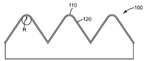
도 1은 본 개시 내용의 실시 형태의 구조화된 반사 필름의 단면을 보여준다.
도 2는 구조물의 곡률 반경을 예시하기 위해 하나의 구조물 상에 중첩시켜 놓은 원이 있는 도 1의 구조화된 반사 필름의 단면도를 보여준다.
도 3은 구조물의 곡률 반경을 예시하기 위해 중첩시켜 놓은 원이 있는 도 2의 구조물의 확대도를 보여준다.
예시된 실시 형태의 하기 설명에서, 본 개시 내용이 실시될 수 있는 다양한 실시 형태가 예시로서 도시된, 첨부 도면을 참조한다. 그 실시 형태들이 이용될 수 있고, 본 발명의 범주로부터 벗어남이 없이 구조적 변화가 이루어질 수 있음이 이해되어야 한다. 도면들은 반드시 일정한 축척으로 도시된 것은 아니다. 도면에 사용된 유사한 도면 부호는 유사한 구성 요소를 지칭한다. 그러나, 주어진 도면에서 구성요소를 지칭하기 위한 도면 부호의 사용은 동일한 도면 부호로 표기된 또 다른 도면의 그 구성요소를 제한하고자 의도되지 않은 것으로 이해되어야 할 것이다.This application is more fully understood when the following detailed description of the various embodiments of the invention is taken in conjunction with the accompanying drawings.
Figure 1 shows a cross-section of a structured reflective film of an embodiment of the present disclosure.
Figure 2 shows a cross-sectional view of the structured reflective film of Figure 1 with a circle superimposed on one structure to illustrate the radius of curvature of the structure.
Fig. 3 shows an enlarged view of the structure of Fig. 2 with circles superimposed to illustrate the radius of curvature of the structure.
In the following description of the illustrated embodiments, reference is made to the accompanying drawings, in which are shown, by way of illustration, various embodiments in which the present disclosure may be practiced. It is to be understood that the embodiments may be utilized and that structural changes may be made without departing from the scope of the present invention. The drawings are not necessarily drawn to scale. Like reference numerals used in the drawings indicate like elements. It should be understood, however, that the use of reference numerals to designate elements in the given drawings is not intended to limit those elements of another drawing depicted with the same reference numerals.
태양광 모듈은 광기전 태양광 전지들의 라미네이트된 어레이(array)로서 일반적으로 제조된다. 어레이는 유리 또는 투명한 중합체 재료와 같이, 일반적으로 투명한 지지 층과, 또한 일반적으로 투명하고 지지 층과 동일한 재료 또는 상이할 수 있는 재료인 커버 층 사이에 존재한다. 태양광 전지 자체는 상당히 작고, 모듈의 총 표면의 단지 일부만을 커버하기 때문에, 더욱 많은 태양광을 태양광 전지 상으로 향하도록 하여 모듈의 효율을 증가시키기 위한 다양한 기술이 개발되어 왔다. 미국 특허 제4,235,643호 (아믹(Amick))에 기재된 일 기술에서는, 복수의 광-반사성 절삭면(facet)을 갖는 광학 매질이 인접 전지들 사이에 배치된다. 광-반사성 절삭면은 서로 모이는 두 개의 절삭면에 의해 형성된 꼭지점에서의 각이 110° 내지 130°, 바람직하게는 약 120°인 복수의 홈(groove)을 규정하도록 각지게 배치된다. 이들 절삭면의 결과는, 절삭면 상에 부딪치는 광이 임계각보다 더 큰 각으로 투명한 전면 커버 부재(member) 내로 다시 반사되어 돌아올 것이고, 그 후 태양광 전지 상에 부딪치기 위하여 커버 부재의 전면 표면으로부터 내부적으로 다시 반사되는 것이다. 미국 특허 제5,994,641호 (카르다우스카스(Kardauskas))에서, 가요성 반사기 수단은 복수의 홈을 갖는 광학 매질로서 사용된다. 가요성 반사기 수단은 은 또는 알루미늄과 같은 반사성 금속의 코팅을 갖는 광학적으로 반사성인 시트 재료이다. 반사성 시트 재료의 절삭면은 뾰족한 피크를 갖는다.Photovoltaic modules are generally fabricated as laminated arrays of photovoltaic photovoltaic cells. The array is generally between a transparent support layer, such as a glass or transparent polymeric material, and also between the cover layer, which is generally transparent and the same or a different material as the support layer. Various techniques have been developed to increase the efficiency of the module by directing more sunlight onto the photovoltaic cell because the photovoltaic cell itself is quite small and covers only a portion of the total surface of the module. In one technique described in U.S. Patent No. 4,235,643 (Amick), an optical medium having a plurality of light-reflective cutting facets is disposed between adjacent cells. The light-reflective cutting surface is angled so as to define a plurality of grooves whose angles at the vertices formed by the two cutting surfaces that converge with each other are 110 ° to 130 °, preferably about 120 °. The result of these cutting planes is that the light hitting the cutting surface will be reflected back into the front cover member transparent at an angle greater than the critical angle and then return to the front surface of the cover member Lt; / RTI > In U.S. Patent No. 5,994,641 (Kardauskas), the flexible reflector means is used as an optical medium having a plurality of grooves. The flexible reflector means is an optically reflective sheet material having a coating of a reflective metal such as silver or aluminum. The cutting surface of the reflective sheet material has a sharp peak.
이 개시 내용에서, 태양광 모듈에서 유용한 (때때로 광 지시 매질로 지칭되는) 반사 필름이 기재된다. 그러한 반사 필름은 일반적으로 편평한 배면 표면 및 구조화된 전면 표면을 갖는다. 구조화된 전면 표면은 둥근 피크를 갖는 미세구조물의 어레이를 포함한다. 이들 둥근 피크의 반사 필름은 앞서 기재된 뾰족한 피크의 반사 필름에 비하여 다양한 장점을 갖는다.In this disclosure, reflective films useful in photovoltaic modules (sometimes referred to as light indicating media) are described. Such a reflective film generally has a flat back surface and a structured front surface. The structured front surface comprises an array of microstructures with rounded peaks. The reflective film of these round peaks has various advantages over the reflective film of the sharp peak described above.
뾰족한 피크의 반사 필름에 대하여 둥근 피크의 반사 필름의 하나의 장점은 반사성 금속 층을 이용한 피크의 코팅에 관련된다. 전형적으로, 반사 필름의 반사 층은 금속 코팅 층이다. 금속 코팅은 금속 기화 기술에 의하여 전형적으로 수행된다. 금속 층의 둥근 피크 상으로의 침적은 뾰족한 피크 상으로의 침적보다 더욱 용이하다. 그러나, 심지어는 침적 용이성보다 더욱 중요한 것으로는, 피크가 뾰족할 때, 즉 피크가 정점으로 도달할 때, 뾰족한 피크를 금속 층으로 적절하게 커버하는 것이 매우 어렵다는 사실이다. 이는, 그리고 종종, 금속이 적거나 존재하지 않은 절삭면의 피크에서 "핀홀(pinhole)"이 결과로서 생성될 수 있다. 이들 핀홀은 광을 반사시키지 않을 뿐 아니라, 중합체 재료가 금속으로 부적절하게 커버되기 때문에, 태양광이 통과되어 절삭면의 중합체 재료에 부딪치는 것이 가능하게 된다. 시간이 흐름에 따라, 태양광은 절삭면의 중합체 재료를 분해시킬 수 있고, 절삭면 및 따라서 일반적으로 반사 필름의 구조적 온전성을 위태롭게 할 수 있다.One advantage of a rounded peak reflective film with respect to a sharp peak reflective film relates to the coating of the peak with the reflective metal layer. Typically, the reflective layer of the reflective film is a metal coated layer. The metal coating is typically performed by metal vaporization techniques. Deposition of the metal layer onto a round peak is easier than deposition onto a sharp peak. However, even more important than the ease of deposition is the fact that it is very difficult to adequately cover the sharp peak with the metal layer when the peak is sharp, i.e. when the peak reaches the apex. This can, and often, result in "pinholes" at the peaks of the cut surface with little or no metal. These pinholes not only do not reflect light but also allow the sunlight to pass through and hit the polymeric material on the cutting surface because the polymeric material is inappropriately covered with metal. Over time, sunlight can degrade the polymeric material on the cutting surface and can jeopardize the cutting surface and hence the structural integrity of the reflective film in general.
다른 한편에서 둥근 피크의 필름은 뾰족한 피크를 갖지 않아, 따라서 코팅이 더욱 용이하다. 이는, 피크의 형태가 뾰족한 지점에 도달하기보다는 점차적으로 변화하기 때문이다. 피크가 둥글고 뾰족한 피크로 도달되지 않기 때문에, 이는 편평한 필름을 코팅하는 것과 같으며, 결과적으로 균일한 금속 코팅을 제공하는 것이 더욱 용이하다. 더욱 중요하게는, 핀 홀의 위험이 감소되거나 또는 제거된다.On the other hand, the film of the round peak does not have a sharp peak, and therefore the coating is easier. This is because the shape of the peak gradually changes rather than reaching a sharp point. Since the peaks are not reached with a rounded, pointed peak, this is like coating a flat film and consequently it is easier to provide a uniform metal coating. More importantly, the risk of pinholes is reduced or eliminated.
뾰족한 피크의 반사 필름에 비하여 둥근 피크의 필름의 또다른 장점은 이들 필름의 취급에 관련된다. 일단, 절삭면이 필름 표면 내로 통합되면, 각종 취급 단계들이 연관된다. 예를 들어, 절삭면을 반사성 금속 층으로 코팅하는 데 연관된 각종 취급 단계가 존재한다. 많은 경우에서, 필름은 절삭면이 필름 표면 내로 통합되는 곳과 상이한 장소에서 금속으로 코팅된다. 종종 필름은 감겨서, 운송되며, 다시 펼쳐져서 금속 코팅이 적용되고, 그 후 필름은 다시 감긴다. 금속 코팅된 필름은 종종 그 후 또 다른 장소로 운송되어 필름 시트가 적절한 크기 및 형태의 유용한 용품이 되도록 한다. 이 공정은 전형적으로 필름 기술 분야에서 "전환"으로서 지칭된다. 필름이 전환될 때, 이들은 다시 펼쳐지고, 필름은 길게 잘리거나(slit), 바람직한 크기 및 형태로 절단되고, 그 후 태양광 모듈로의 통합을 위하여 또 다른 장소로의 수송을 위해 포장될 수 있다. 이러한 일련의 단계에서의 많은 변화들이 가능하며, 태양광 모듈에의 부착을 위해 접착제 층을 필름 용품에 라미네이팅하는 것과 같은 추가의 단계 또한 사용될 수 있다. 예를 들어, 구조화 (절단면을 필름 내로 통합), 금속 코팅, 및 전환이 단일한 장소에서 연속 공정으로서 수행되는 것이 가능할 수 있지만, 심지어는 그러한 통합된 공정에서도, 필름 용품을 태양광 모듈 어셈블리 장소 및 태양광 모듈의 어셈블리 자체로 수송하는 단계는 말할 것도 없이, 취급 단계가 여전히 존재한다. 뾰족한 피크 필름을 이용하는 경우, 이들 각 취급 단계는 뾰족한 피크가 손상될 가능성을 제공한다. 이는 필름이 그 자체로 감겨있고 뾰족한 피크가 필름의 배면에 접촉하는 공정을 이용하는 경우 특히 그렇다. 뾰족한 피크에의 손상은 필름의 미적 외관에 영향을 줄 뿐만 아니라, 태양광을 반사시키는 필름의 능력을 약화시킬 수 있다. 이러한 손상은 필름 자체의 피크에 일어날 수 있거나, 반사성 금속 층으로 코팅된 후에 피크에 일어날 수 있거나, 필름 및 금속 코팅된 필름에 대한 손상의 조합이 가능하다.Another advantage of a film with a rounded peak compared to a reflective film with a sharp peak relates to the handling of these films. Once the cutting surface is incorporated into the film surface, various handling steps are involved. For example, there are various handling steps associated with coating the cut surface with a reflective metal layer. In many cases, the film is coated with a metal at a different location than where the cutting surface is integrated into the film surface. Often the film is wrapped, transported, re-stretched, applied with a metal coating, and then the film is rewound. The metal coated film is often then transported to another location so that the film sheet becomes a useful article of the appropriate size and shape. This process is typically referred to as "conversion" in the field of film technology. When the films are switched, they are unfolded again, and the film is slit, cut to the desired size and shape, and then packaged for transport to another location for integration into the photovoltaic module. Many variations in this series of steps are possible and additional steps such as laminating the adhesive layer to the film article for attachment to a solar module may also be used. For example, although it may be possible for structuring (incorporating cut surfaces into a film), metal coating, and conversion to be performed as a continuous process in a single place, even in such an integrated process, Needless to say, the handling stage still exists, not to mention the transport of the solar module itself. If a sharp peak film is used, each of these handling steps provides the possibility of a sharp peak being damaged. This is especially true when the film is wound by itself and a sharp peak is used to contact the backside of the film. Damage to sharp peaks not only affects the aesthetic appearance of the film, but it can also weaken the ability of the film to reflect sunlight. Such damage can occur at the peak of the film itself, or can occur at the peak after being coated with the reflective metal layer, or a combination of damage to the film and the metal coated film is possible.
한편 둥근 피크 필름은 취급이 보다 쉽고, 가공, 수송, 전환 및 다른 취급 단계 동안 손상되기 쉬운 뾰족한 피크가 없다.On the other hand, rounded peak films are easier to handle and have no sharp peaks that are susceptible to damage during processing, transport, conversion and other handling steps.
달리 지시되지 않는 한, 본 명세서 및 청구범위에 사용되는 특징부 크기, 양 및 물리적 특성을 표현하는 모든 수치는 모든 경우 용어 "약"에 의해 수식되는 것으로 이해되어야 한다. 따라서, 반대로 지시되지 않는 한, 상기 명세서 및 첨부된 청구범위에 기술된 수치적 파라미터는 본 명세서에 개시된 교시를 이용하는 당업자가 얻고자 하는 원하는 특성에 따라 변할 수 있는 근사치이다. 종점(endpoint)들에 의한 수치 범위의 설명은 범위 내에 포함되는 모든 숫자 (예를 들어, 1 내지 5는 1, 1.5, 2, 2.75, 3, 3.80, 4 및 5를 포함함) 및 범위 내의 임의의 범위를 포함한다.Unless otherwise indicated, all numbers expressing feature sizes, amounts, and physical characteristics used in the present specification and claims are to be understood as being modified in all instances by the term "about ". Accordingly, unless indicated to the contrary, the numerical parameters set forth in the foregoing specification and appended claims are approximations that may vary depending upon the desired properties to be gained by those skilled in the art using the teachings disclosed herein. The description of a numerical range by endpoints is intended to encompass all numbers contained within the range (e.g., 1 to 5 include 1, 1.5, 2, 2.75, 3, 3.80, 4 and 5) ≪ / RTI >
본 명세서 및 첨부된 청구범위에 사용되는 바와 같이, 단수 형태("a", "an" 및 "the")는 그 내용이 명백하게 다르게 지시하지 않는 한 복수의 지시 대상을 갖는 실시 형태를 포함한다. 예를 들어, "층"에 대한 언급은 1개, 2개 또는 그 이상의 층을 갖는 실시 형태들을 포함한다. 본 명세서 및 첨부된 청구범위에서 사용될 때, 용어 "또는"은 일반적으로 그 내용이 명백하게 달리 지시하지 않는 한 "및/또는"을 포함하는 그의 의미로 이용된다.As used in this specification and the appended claims, the singular forms "a," "an," and "the" include embodiments having a plurality of referents unless the context clearly dictates otherwise. For example, reference to "layer" includes embodiments having one, two, or more layers. As used in this specification and the appended claims, the term "or" is generally used in its sense including "and / or" unless the content clearly dictates otherwise.
본 명세서에 사용되는 바와 같이, 미세구조 특징부, 특히 복수의 미세구조를 설명하는데 사용된 경우, 용어 "정렬된 배열"은, 자연 표면 조도 또는 다른 자연적 특징부와 상이한 부여된 패턴을 의미하며, 여기에서 배열은 연속적 또는 비연속적일 수 있으며, 반복 패턴, 비-반복 패턴, 랜덤 패턴 등일 수 있다.As used herein, the term "aligned array " when used to describe microstructural features, particularly a plurality of microstructures, refers to a given pattern that differs from a natural surface roughness or other natural feature, The array may be continuous or non-continuous, and may be a repeating pattern, a non-repeating pattern, a random pattern, or the like.
본 명세서에 사용되는 바와 같이, 용어 "미세구조"는, 특징부의 2개 이상의 치수가 미시적인, 특징부의 형태를 의미한다. 특징부의 부분도 및/또는 단면도가 미시적이어야 한다.As used herein, the term "microstructure" means a feature of a feature in which at least two dimensions of the feature are microscopic. Partial views and / or cross-sectional views of the features should be microscopic.
본 명세서에 사용되는 바와 같이, 용어 "미시적"은 그 형태를 결정하기 위하여 임의의 시계 면(plane of view)으로부터 볼 때 육안에 광학적 도움(optic aid)이 필요할 정도로 충분히 작은 치수의 특징부를 말한다. 일 기준은 문헌 [W. J. 스미스(Smith)의, 모뎀 옵틱 엔지니어링 (Modem Optic Engineering), 맥그로-힐 (McGraw-Hill), 1966, p.104-105]에서 찾을 수 있으며, 이에 의하면 시력,"... 은 인식될 수 있는 최소 캐릭터(character)의 각 크기(angular size) 면에서 정의 및 측정된다." 정상 시력은 최소 인식가능 문자가 망막 상에서 호(arc)의 각도 높이 5분에 대응할 때인 것으로 고려된다. 250 mm (10 인치)의 전형적인 작업 거리에서, 이것은 이 대상에 대해 0.36 mm (0.0145 인치)의 측면 치수를 생성한다.As used herein, the term "micro" refers to a feature of a dimension sufficiently small to require an optical aid in the naked eye when viewed from any plane of view to determine its shape. The day standard is described in W. Can be found in J. Smith, Modem Optic Engineering, McGraw-Hill, 1966, p. 104-105, whereby vision, " Defined and measured in terms of the angular size of the minimum character that can be ". The normal visual acuity is considered to be when the least recognizable character corresponds to an angular height of arc 5 minutes on the retina. At a typical working distance of 250 mm (10 inches), this creates a side dimension of 0.36 mm (0.0145 inch) for this object.
용어 "(메트)아크릴레이트"는 알코올의 단량체성 아크릴산 에스테르 또는 메타크릴산 에스테르를 지칭한다. 아크릴레이트 및 메타크릴레이트 단량체 또는 올리고머는 본 명세서에서 총체적으로 "(메트)아크릴레이트"로 지칭된다. "(메트)아크릴레이트계"로 기술된 중합체는 주로 (50 중량% 초과) (메트)아크릴레이트 단량체로부터 제조된 중합체 또는 공중합체이며, 추가의 에틸렌계 불포화 단량체를 포함할 수 있다.The term "(meth) acrylate" refers to monomeric acrylic or methacrylic acid esters of alcohols. Acrylate and methacrylate monomers or oligomers are collectively referred to herein as "(meth) acrylates ". Polymers described as "(meth) acrylate-based" are polymers or copolymers primarily made from (greater than 50% by weight) (meth) acrylate monomers and may include additional ethylenically unsaturated monomers.
달리 지시되지 않는다면, "광학적으로 투과성인(optically transparent)"은 가시광 스펙트럼(약 400 내지 약 700 nm)의 적어도 일부분에 걸쳐 높은 광투과율을 갖는 물품, 필름 또는 접착제 조성물을 지칭한다.Unless otherwise indicated, "optically transparent" refers to an article, film or adhesive composition having a high light transmittance over at least a portion of the visible light spectrum (from about 400 to about 700 nm).
2개의 층을 언급할 때, 본 명세서에 사용되는 바와 같은 용어 "인접한"은 2개의 층이, 이들 사이에 개입하는 개방 공간 없이 서로 근접해 있는 것을 의미한다. 그들은 (예를 들어, 함께 라미네이팅되어) 서로 직접 접촉할 수 있거나 또는 개입 층이 있을 수 있다.When referring to two layers, the term "adjacent " as used herein means that the two layers are in close proximity to one another without any open space intervening therebetween. They may be in direct contact with each other (for example, laminated together) or there may be an intervening layer.
본 명세서에서 사용되는 바와 같은 용어, "임계각"은 입사각이 더욱 짙은 광학 매질로부터 덜 짙은 광학 매질로 통과하는 광선에 대해 가질 수 있는 가장 큰 값을 지칭한다. 입사각의 각이 임계각을 초과하는 경우, 광선은 덜 짙은 매질로 들어가지 않을 것이지만, 완전히 내부적으로 다시 덜 짙은 매질 내로 반사될 것이다.The term "critical angle " as used herein refers to the largest value that can be had for a ray passing from a more intense optical medium to a lesser optical medium. If the angle of incidence exceeds the critical angle, the light will not enter the less dense medium, but will be totally internally reflected back into the darker medium.
본 명세서에는 태양광 모듈의 제조에서의 이용에 적합한 반사 필름이 개시된다. 이들 필름은 기저 층, 및 기저 층으로부터 돌출된 복수의 미세구조물의 정렬된 배열을 포함하고, 상기 미세구조물은 둥근 피크를 갖고, 반사 층을 포함한다.A reflective film suitable for use in the manufacture of solar modules is disclosed herein. These films include an underlying layer and an ordered array of a plurality of microstructures protruding from the base layer, the microstructure having a rounded peak and including a reflective layer.
도 1은 본 개시 내용의 미세구조화된 반사 필름의 단면도를 보여준다. 도 1에서, 반사 필름(100)은, 둥근 피크인, 미세구조화된 특징부(110), 및 반사 층(120)을 포함한다. 전형적으로, 반사 층(120)은 은 또는 알루미늄, 비용 문제로 인해 더욱 전형적으로는 알루미늄을 포함하는 반사성 금속 코팅 층이다. 미세구조물은 기저 층으로부터 5 마이크로미터 내지 500 마이크로미터 튀어나와 있다.Figure 1 shows a cross-sectional view of a microstructured reflective film of the present disclosure. In FIG. 1, the
둥근 미세구조물은 곡률 반경을 갖는 것으로서 설명될 수 있다. 이러한 곡률 반경은, 도 1에 나타낸 것과 같은 필름(100)의 단면인 도 2에, 둥근 미세구조물들 중 하나 위에 중첩시킨 원을 이용하여 나타내었다. 중첩된 원은 반경 R을 갖고, 이 반경 R은 곡률 반경으로서 정의된다. 전형적으로, 곡률 반경은 0.1 내지 5.0 마이크로미터, 더욱 전형적으로는 0.2 내지 5.0 마이크로미터이다.The round microstructure can be described as having a radius of curvature. This radius of curvature is shown in Figure 2, which is a cross section of the
도 3은, 반경 R을 갖는 중첩된 원을 나타내는, 도 2의 필름의 미세구조물들 중 하나의 확대도를 나타내며, 이 반경 R은 곡률 반경을 정의한다.Figure 3 shows an enlarged view of one of the microstructures of the film of Figure 2, representing a superimposed circle with a radius R, which defines the radius of curvature.
기저 층 재료는 중합체 재료를 포함한다. 광범위한 중합체 재료가 기저 층의 제조에 적합하다. 적합한 중합체 재료의 예로는, 셀룰로오스 아세테이트 부티레이트; 셀룰로오스 아세테이트 프로피오네이트; 셀룰로오스 트라이아세테이트; 폴리메틸 메타크릴레이트와 같은 폴리(메트)아크릴레이트; 폴리에틸렌 테레프탈레이트, 및 폴리에틸렌 나프탈레이트와 같은 폴리에스테르; 나프탈렌 다이카르복실산 기재의 공중합체 또는 블렌드; 폴리에테르 설폰; 폴리우레탄; 폴리카르보네이트; 폴리염화비닐; 신디오택틱 폴리스티렌; 환형 올레핀 공중합체; 실리콘계 재료; 및 폴리에틸렌 및 폴리프로필렌을 포함하는 폴리올레핀; 및 이의 블렌드를 포함한다. 기저 층에 특히 적합한 중합체 재료는 폴리올레핀 및 폴리에스테르이다.The base layer material comprises a polymeric material. A wide range of polymeric materials are suitable for the preparation of the base layer. Examples of suitable polymeric materials include, but are not limited to, cellulose acetate butyrate; Cellulose acetate propionate; Cellulose triacetate; Poly (meth) acrylates such as polymethyl methacrylate; Polyesters such as polyethylene terephthalate, and polyethylene naphthalate; Naphthalene dicarboxylic acid based copolymers or blends; Polyethersulfone; Polyurethane; Polycarbonate; Polyvinyl chloride; Syndiotactic polystyrene; Cyclic olefin copolymers; Silicon based materials; And polyolefins including polyethylene and polypropylene; And blends thereof. Particularly suitable polymeric materials for the underlying layer are polyolefins and polyesters.
전형적으로, 미세구조물 또한 중합체 재료를 포함한다. 일부 실시 형태에서, 미세구조물의 중합체 재료는 기저 층과 동일한 조성이다. 다른 실시 형태에서, 미세구조물의 중합체 재료는 기저 층의 재료와 상이하다. 일부 실시 형태에서, 기저 층 재료는 폴리에스테르이고, 미세구조물의 재료는 폴리(메트)아크릴레이트이다.Typically, the microstructure also comprises a polymeric material. In some embodiments, the polymeric material of the microstructure has the same composition as the base layer. In another embodiment, the polymeric material of the microstructure is different from the material of the base layer. In some embodiments, the base layer material is polyester and the material of the microstructure is poly (meth) acrylate.
일부 실시 형태에서, 미세구조화된 필름은 미세구조물을 필름 상에 부여함으로써 제조된다. 이들 실시 형태에서, 기저 층 및 미세구조물은 동일한 중합체 조성물을 포함한다. 다른 실시 형태에서, 미세구조물의 층은 별도로 제조되어, 기저 층에 라미네이트된다. 이 라미네이션은 열, 열 및 압력의 조합, 또는 접착제의 이용을 통하여 수행될 수 있다. 여전히 상이한 실시 형태에서, 미세구조물은 기저 층 상에 형성된다.In some embodiments, the microstructured film is produced by imparting microstructures on the film. In these embodiments, the base layer and the microstructure comprise the same polymer composition. In another embodiment, the layers of microstructures are prepared separately and laminated to the base layer. This lamination can be carried out through a combination of heat, heat and pressure, or through the use of an adhesive. Still in a different embodiment, the microstructure is formed on the base layer.
미세구조화된 필름 또는 미세구조물의 층은 엠보싱에 의해 제조될 수 있다. 이 공정에서, 엠보싱가능한 표면을 갖는 편평한 필름은 압력 및/또는 열의 적용과 함께 구조화된 공구(tool)에 접촉되어 엠보싱된 표면을 형성한다. 편평한 필름 전체가 엠보싱가능한 재료를 포함할 수 있거나, 편평한 필름이 단지 엠보싱가능한 표면을 가질 수 있다. 엠보싱가능한 표면은 편평한 필름의 재료와 상이한 재료의 층을 포함할 수 있으며, 즉 상기 편평한 필름은 그의 표면에서 엠보싱가능한 재료의 코팅을 가질 수 있다. 엠보싱된 표면은 구조화된 표면이다. 엠보싱된 표면 상의 구조는 공구 표면 상에서의 구조의 반대인데, 즉 공구 표면 상의 돌출부가 엠보싱된 표면 상에서 함몰부를 형성할 것이고, 공구 표면 상에서 함몰부는 엠보싱된 표면 상에서 돌출부를 형성할 것이다. 미세구조 특징부는 구조물의 피크가 둥글기만 하다면, 다양한 형태를 취할 수 있다. 둥근 미세구조 특징부의 형성 방법의 일례가, 예를 들어 미국 특허 제6,280,063호 (퐁(Fong), 등)에 기재되어 있다.A layer of microstructured film or microstructure may be produced by embossing. In this process, a flat film having an embossable surface is contacted with a structured tool with application of pressure and / or heat to form an embossed surface. The entire flat film may comprise an embossable material, or the flat film may have only an embossable surface. The embossable surface may comprise a layer of a material different from the material of the flat film, i.e. the flat film may have a coating of an embossable material on its surface. The embossed surface is a structured surface. The structure on the embossed surface is the opposite of the structure on the tool surface, i.e., the protrusions on the tool surface will form depressions on the embossed surface, and the depressions on the tool surface will form protrusions on the embossed surface. The microstructural features can take many forms if the peaks of the structure are rounded. An example of a method of forming a round microstructure feature is described, for example, in U.S. Patent No. 6,280,063 (Fong, et al.).
전형적으로, 미세구조화된 공구는 몰딩(molding) 공구이다. 구조화된 몰딩 공구는 편평한 스탬핑 프레스(stamping press), 가요성 또는 비가요성 벨트 또는 롤러의 형태일 수 있다. 또한, 몰딩 공구는 일반적으로 엠보싱, 코팅, 주조 또는 평압 프레싱(platen pressing)에 의해 표면에 미세구조화된 패턴을 생성시키고, 완성된 용품의 일부가 되지 않는 공구인 것으로 간주된다. 미세구조 특징부를 형성하는데 사용될 수 있는 몰딩 과정의 일례가 PCT 공개 제WO 2012/082391호에 기재되어 있다.Typically, the microstructured tool is a molding tool. The structured molding tool may be in the form of a flat stamping press, a flexible or non-flexible belt or roller. Molding tools are also generally regarded as tools that produce microstructured patterns on the surface by embossing, coating, casting or platen pressing and are not part of the finished article. An example of a molding process that can be used to form the microstructure features is described in PCT Publication No. WO 2012/082391.
미세구조화된 몰딩 공구를 생성하기 위한 광범위한 방법이 당업자에게 알려져 있다. 이들 방법의 예에는 포토리소그래피, 에칭, 방전 가공(discharge machining), 이온 밀링(ion milling), 미세가공(micromachining), 및 전기주조(electroforming)가 포함되지만, 이에 한정되지 않는다. 미세구조화된 몰딩 공구는 또한 가교결합성 액체 실리콘 고무, 방사선 경화성 우레탄 등으로 이루어진 군으로부터 선택되는 것과 같은 몰딩가능성 재료를 이용하여 불규칙적인 형태와 패턴을 포함한 다양한 미세구조화된 표면을 복제하거나, 음각 또는 양각 복제 중간체 또는 최종 엠보싱 공구 몰드를 생성하기 위하여 전기주조(electroforming)하여 다양한 미세구조를 복제함으로써 제조될 수 있다. 또한, 랜덤하고 불규칙적인 형태와 패턴을 갖는 미세구조화된 몰드는 화학적 에칭, 샌드블라스팅, 숏피닝(shot peening) 또는 몰딩가능성 재료 내로의 별개의 구조화된 입자의 침투(sinking)에 의해 생성될 수 있다. 추가적으로 임의의 미세구조화된 몰딩 공구는 미국 특허 제5,122,902호 (벤슨(Benson))에 교시된 절차에 따라 변경되거나 변형될 수 있다. 공구는 주석, 구리, 강철, 또는 금속 합금과 같은 금속, 또는 중합체 재료를 포함하는 광범위한 재료로부터 제조될 수 있다.Extensive methods for producing microstructured molding tools are known to those skilled in the art. Examples of these methods include, but are not limited to, photolithography, etching, discharge machining, ion milling, micromachining, and electroforming. Microstructured molding tools can also be made by replicating a variety of microstructured surfaces, including irregular shapes and patterns, using moldable materials such as those selected from the group consisting of crosslinkable liquid silicone rubber, radiation curable urethane, For example, by electroforming to produce a positive embossing intermediate or a final embossing tool mold to replicate various microstructures. In addition, microstructured molds with random and irregular shapes and patterns can be created by chemical etching, sandblasting, shot peening, or by sinking of separate structured particles into the moldable material . In addition, any microstructured molding tool may be modified or modified in accordance with the procedure taught in U.S. Patent No. 5,122,902 (Benson). The tool can be made from a wide range of materials including metals, such as tin, copper, steel, or metal alloys, or polymeric materials.
상기 언급된 것과 같이, 기저 층 및 미세구조화된 층은 단일한 구조물을 포함할 수 있고, 따라서 동일한 재료로부터 제조된다. 기저 층의 일부인 미세구조화된 층 없이, 미세구조화된 층을 생성하기 위한 몇몇 방법들 또한 존재한다. 예를 들어, 경화성 또는 용융된 중합체 재료는 미세구조화된 몰딩 공구에 대하여 주조되고, 경화 또는 냉각되어 몰드 내에 미세구조화된 층을 형성할 수 있었다. 몰드에서, 이 층은 그 후 열 및/또는 압력에 의해 또는 감압 접착제 또는 경화성 접착제와 같은 접착제의 이용에 의해 중합체 필름에 부착될 수 있었다. 몰딩 공구를 그 후 제거하여 기저 층 및 미세구조화된 층을 갖는 구조물을 생성할 수 있었다. 이 공정의 변형에서, 상기 미세구조화된 몰딩 공구 내의 용융된 또는 경화성 중합체 재료는 필름에 접촉되고 그 후 경화 또는 냉각될 수 있었다. 경화 또는 냉각 공정에서, 몰딩 공구 내 중합체 재료는 필름에 부착될 수 있다. 몰딩 공구 제거시, 기저 층 (상기 필름) 및 미세구조화된 층을 포함하는 구조물이 형성된다. 일부 실시 형태에서, 미세구조화된 층은 방사선 경화성 (메트)아크릴레이트 재료로부터 제조되고, 몰딩된 (메트)아크릴레이트 재료는 화학 방사선에의 노출에 의해 경화된다.As mentioned above, the base layer and the microstructured layer may comprise a single structure and are therefore made from the same material. Without the microstructured layer being a part of the base layer, there are also some methods for creating a microstructured layer. For example, the curable or molten polymeric material can be cast onto a microstructured molding tool and cured or cooled to form a microstructured layer in the mold. In the mold, this layer could then be attached to the polymer film by heat and / or pressure or by use of an adhesive such as a pressure sensitive adhesive or a curable adhesive. The molding tool could then be removed to create a structure having a base layer and a microstructured layer. In a variation of this process, the molten or curable polymeric material in the microstructured molding tool can be contacted with the film and then cured or cooled. In the curing or cooling process, the polymeric material in the molding tool can be attached to the film. Upon removal of the molding tool, a structure comprising a base layer (the film) and a microstructured layer is formed. In some embodiments, the microstructured layer is made from a radiation curable (meth) acrylate material and the molded (meth) acrylate material is cured by exposure to actinic radiation.
미세구조물의 층은 그의 표면 상에서 반사 층을 갖는다. 예를 들어 반사성 금속 코팅과 같은 임의의 적합한 반사 층이 사용될 수 있다. 반사성 금속 코팅이 사용된 경우, 코팅은 전형적으로 은, 알루미늄, 또는 그의 조합이다. 알루미늄이 더욱 전형적이지만, 임의의 적합한 금속 코팅이 사용될 수 있다. 일반적으로, 금속 층은, 잘 이해되고 있는 절차를 이용하여, 증착에 의해 코팅된다. 금속성 코팅은 매우 얇으며, 일반적으로 약 300 내지 1000 옹스트롬 두께, 더욱 전형적으로는 300 내지 500 옹스트롬이다.The layer of microstructure has a reflective layer on its surface. Any suitable reflective layer, such as, for example, a reflective metal coating, may be used. When a reflective metallic coating is used, the coating is typically silver, aluminum, or a combination thereof. Although aluminum is more typical, any suitable metal coating may be used. Generally, the metal layer is coated by vapor deposition, using well understood procedures. The metallic coating is very thin, typically about 300 to 1000 angstroms thick, and more typically 300 to 500 angstroms.
태양광 모듈 또한 본 명세서에서 개시된다. 이들 태양광 모듈은 복수의 태양광 전지, 및 기저 층으로부터 돌출된 복수의 미세구조물을 포함하는 반사 필름을 포함하고, 상기 미세구조물은 둥근 피크를 갖고, 반사 층을 포함한다. 반사 필름은 상기 기재되었다. 태양광 전지의 어레이는 유리 또는 투명한 중합체 재료와 같이, 일반적으로 투명한 지지 층과, 또한 일반적으로 투명하고 지지 층과 동일한 재료 또는 상이할 수 있는 재료인 커버 층 사이에 일반적으로 존재한다.Solar modules are also disclosed herein. These photovoltaic modules include a plurality of photovoltaic cells, and a reflective film comprising a plurality of microstructures protruding from the base layer, wherein the microstructures have rounded peaks and include a reflective layer. The reflective film was described above. The array of photovoltaic cells is generally present between a generally transparent support layer, such as a glass or transparent polymeric material, and also between the cover layer, which is generally transparent and the same or a different material as the support layer.
태양광 모듈의 제조 방법 또한 본 명세서에 개시된다. 이들 방법은, 반사 필름을 제공하는 단계로, 상기 반사 필름은 기저 층으로부터 돌출된 복수의 미세구조물을 포함하고, 상기 미세구조물은 둥근 피크를 갖고, 반사 층을 포함하는 단계, 지지 기재 상에 배열되고 태빙 리본에 의해 접속된 복수의 태양광 전지를 제공하는 단계, 반사 필름을 태양광 전지 및 인접 영역에 부착시키는 단계, 및 투명한 커버 층을 반사 필름 위로 부착시키는 단계를 포함한다. 반사 필름은 상기 기재되었다.Methods of making solar modules are also disclosed herein. The method comprises the steps of providing a reflective film, wherein the reflective film comprises a plurality of microstructures protruding from the base layer, the microstructure having a round peak, comprising a reflective layer, arranged on the support substrate Providing a plurality of solar cells connected by a tabbing ribbon, attaching a reflective film to the solar cell and adjacent areas, and attaching a transparent cover layer over the reflective film. The reflective film was described above.
일부 실시 형태에서, 반사 필름은 태빙 리본에 인접하여 배치된다. 태빙 리본 (전기 접속기)은 불활성인 그늘진 영역, 즉 이들 영역에 부딪치는 광이 광기전성 전환에 사용되지 않는 영역을 생성한다. 따라서 이들 태빙 리본에 인접한 반사 필름의 배치는 태양광 모듈에 의해 생성된 에너지를 증가시킬 수 있고, 이는 2013년 3월 27일 출원된 미국 특허 변호인 일람 번호 제69734US002호에 설명되어 있는 바와 같다.In some embodiments, the reflective film is disposed adjacent to the tableting ribbon. The tabbing ribbons create shaded areas that are inert, i.e., areas where light striking these areas is not used for photovoltaic conversion. Thus, the placement of reflective films adjacent to these tabbing ribbons can increase the energy produced by the photovoltaic modules, as described in U.S. Patent Attorney Docket No. 69734US002, filed March 27,
Claims (21)
기저 층; 및
기저 층으로부터 돌출된 복수의 미세구조물의 정렬된 배열을 포함하고,
상기 미세구조물은 둥근 피크를 갖고, 반사 층을 포함하는, 반사 필름.As a reflective film,
A base layer; And
An aligned array of a plurality of microstructures protruding from the base layer,
Wherein the microstructure has a round peak and comprises a reflective layer.
복수의 태양광 전지; 및
반사 필름을 포함하고, 상기 반사 필름은:
기저 층; 및
기저 층으로부터 돌출된 복수의 미세구조물의 정렬된 배열을 포함하고,
상기 미세구조물은 둥근 피크를 갖고,
반사 층을 포함하는, 태양광 모듈.As a solar module:
A plurality of photovoltaic cells; And
Wherein the reflective film comprises:
A base layer; And
An aligned array of a plurality of microstructures protruding from the base layer,
The microstructure has a round peak,
And a reflective layer.
반사 필름을 제공하는 단계 - 반사 필름은:
기저 층; 및
기저 층으로부터 돌출된 복수의 미세구조물의 정렬된 배열을 포함하고,
상기 미세구조물이 둥근 피크를 갖고,
반사 층을 포함함 -;
지지 기재 상에 배열되고,
태빙 리본에 의해 접속된 복수의 태양광 전지를 제공하는 단계;
반사 필름을 태양광 전지 및/또는 인접 영역에 부착시키는 단계; 및
반사 필름 위에 투명한 커버 층을 부착시키는 단계를 포함하는, 제조 방법.A method for manufacturing a solar module, comprising:
Providing a reflective film - the reflective film comprises:
A base layer; And
An aligned array of a plurality of microstructures protruding from the base layer,
Wherein the microstructure has a round peak,
A reflective layer;
Arranged on a support substrate,
Providing a plurality of photovoltaic cells connected by a tableting ribbon;
Attaching a reflective film to the photovoltaic cell and / or adjacent areas; And
And attaching a transparent cover layer over the reflective film.
Applications Claiming Priority (3)
| Application Number | Priority Date | Filing Date | Title |
|---|---|---|---|
| US201361843953P | 2013-07-09 | 2013-07-09 | |
| US61/843,953 | 2013-07-09 | ||
| PCT/US2014/045029 WO2015006097A1 (en) | 2013-07-09 | 2014-07-01 | Reflecting films with rounded microstructures for use in solar modules |
Publications (1)
| Publication Number | Publication Date |
|---|---|
| KR20160030529A true KR20160030529A (en) | 2016-03-18 |
Family
ID=51213050
Family Applications (1)
| Application Number | Title | Priority Date | Filing Date |
|---|---|---|---|
| KR1020167002595A KR20160030529A (en) | 2013-07-09 | 2014-07-01 | Reflecting films with rounded microstructures for use in solar modules |
Country Status (6)
| Country | Link |
|---|---|
| US (1) | US20160172517A1 (en) |
| EP (1) | EP3020074A1 (en) |
| JP (1) | JP2016525707A (en) |
| KR (1) | KR20160030529A (en) |
| CN (1) | CN105359281A (en) |
| WO (1) | WO2015006097A1 (en) |
Families Citing this family (4)
| Publication number | Priority date | Publication date | Assignee | Title |
|---|---|---|---|---|
| WO2013148149A1 (en) | 2012-03-27 | 2013-10-03 | 3M Innovative Properties Company | Photovoltaic modules comprising light directing mediums and methods of making the same |
| EP3362744A4 (en) | 2015-10-12 | 2019-06-12 | 3M Innovative Properties Company | Light redirecting film useful with solar modules |
| CN107561612A (en) * | 2017-10-17 | 2018-01-09 | 张家港康得新光电材料有限公司 | Reflective membrane and its application and grid line structure and solar panel |
| CN108020875A (en) * | 2017-12-28 | 2018-05-11 | 常州华威新材料有限公司 | Resistance to compression reflective membrane resistant to lodging and preparation method thereof |
Family Cites Families (24)
| Publication number | Priority date | Publication date | Assignee | Title |
|---|---|---|---|---|
| US4235643A (en) | 1978-06-30 | 1980-11-25 | Exxon Research & Engineering Co. | Solar cell module |
| US4751191A (en) | 1987-07-08 | 1988-06-14 | Mobil Solar Energy Corporation | Method of fabricating solar cells with silicon nitride coating |
| US5122902A (en) | 1989-03-31 | 1992-06-16 | Minnesota Mining And Manufacturing Company | Retroreflective articles having light-transmissive surfaces |
| US5074920A (en) | 1990-09-24 | 1991-12-24 | Mobil Solar Energy Corporation | Photovoltaic cells with improved thermal stability |
| US5118362A (en) | 1990-09-24 | 1992-06-02 | Mobil Solar Energy Corporation | Electrical contacts and methods of manufacturing same |
| US5178685A (en) | 1991-06-11 | 1993-01-12 | Mobil Solar Energy Corporation | Method for forming solar cell contacts and interconnecting solar cells |
| US5320684A (en) | 1992-05-27 | 1994-06-14 | Mobil Solar Energy Corporation | Solar cell and method of making same |
| US5478402A (en) | 1994-02-17 | 1995-12-26 | Ase Americas, Inc. | Solar cell modules and method of making same |
| US6280063B1 (en) | 1997-05-09 | 2001-08-28 | 3M Innovative Properties Company | Brightness enhancement article |
| JP3670835B2 (en) * | 1998-04-22 | 2005-07-13 | 三洋電機株式会社 | Solar cell module |
| US5994641A (en) * | 1998-04-24 | 1999-11-30 | Ase Americas, Inc. | Solar module having reflector between cells |
| US20070125415A1 (en) * | 2005-12-05 | 2007-06-07 | Massachusetts Institute Of Technology | Light capture with patterned solar cell bus wires |
| US8581094B2 (en) | 2006-09-20 | 2013-11-12 | Dow Global Technologies, Llc | Electronic device module comprising polyolefin copolymer |
| JP5436805B2 (en) * | 2008-07-04 | 2014-03-05 | 三洋電機株式会社 | Solar cell module |
| KR20110084404A (en) * | 2008-10-03 | 2011-07-22 | 도판 인사츠 가부시키가이샤 | Solar battery module |
| US20110240095A1 (en) * | 2008-11-19 | 2011-10-06 | Toppan Printing Co., Ltd. | Light reuse sheet, solar battery module, and light source module |
| WO2010058589A1 (en) * | 2008-11-19 | 2010-05-27 | 凸版印刷株式会社 | Light reusing sheet and solar battery module |
| JP4706759B2 (en) * | 2009-01-23 | 2011-06-22 | トヨタ自動車株式会社 | Solar cell |
| JP2010147454A (en) * | 2009-04-03 | 2010-07-01 | Toppan Printing Co Ltd | Optical reuse sheet for solar cell module, and solar cell module |
| JP5568885B2 (en) * | 2009-04-03 | 2014-08-13 | 凸版印刷株式会社 | Solar cell module |
| JP2011108725A (en) * | 2009-11-13 | 2011-06-02 | Toppan Printing Co Ltd | Back sheet, solar battery back sheet, and solar battery module using the same |
| CN103260897B (en) | 2010-12-14 | 2016-08-24 | 3M创新有限公司 | Image and its manufacture method |
| EP2466648A1 (en) * | 2010-12-16 | 2012-06-20 | SolarWorld Innovations GmbH | Tabbing ribbon, photovoltaic solar panel, method for manufacturing a solar cell tabbing ribbon, machine for manufacturing a solar cell tabbing ribbon |
| US20160172518A1 (en) * | 2013-07-09 | 2016-06-16 | 3M Innovative Properties Company | Reflective microstructured films with microstructures having curved surfaces, for use in solar modules |
-
2014
- 2014-07-01 JP JP2016525376A patent/JP2016525707A/en active Pending
- 2014-07-01 EP EP14742113.5A patent/EP3020074A1/en not_active Withdrawn
- 2014-07-01 KR KR1020167002595A patent/KR20160030529A/en not_active Application Discontinuation
- 2014-07-01 WO PCT/US2014/045029 patent/WO2015006097A1/en active Application Filing
- 2014-07-01 CN CN201480038516.3A patent/CN105359281A/en active Pending
- 2014-07-01 US US14/902,660 patent/US20160172517A1/en not_active Abandoned
Also Published As
| Publication number | Publication date |
|---|---|
| JP2016525707A (en) | 2016-08-25 |
| CN105359281A (en) | 2016-02-24 |
| US20160172517A1 (en) | 2016-06-16 |
| EP3020074A1 (en) | 2016-05-18 |
| WO2015006097A1 (en) | 2015-01-15 |
Similar Documents
| Publication | Publication Date | Title |
|---|---|---|
| US10903382B2 (en) | Light redirecting film useful with solar modules | |
| CN107845697B (en) | Adhesive for light redirecting films | |
| US20160172518A1 (en) | Reflective microstructured films with microstructures having curved surfaces, for use in solar modules | |
| US20180040757A1 (en) | Light redirecting film useful with solar modules | |
| KR20160030529A (en) | Reflecting films with rounded microstructures for use in solar modules | |
| CN113169237B (en) | Photovoltaic module | |
| EP3214659A1 (en) | Bi-facial photovoltaic device comprising a rear texture | |
| JP2016525707A5 (en) | ||
| US20190305165A1 (en) | Photovoltaic module | |
| US20210313482A1 (en) | Light redirecting film having stray-light mitigation properties useful with solar modules | |
| US20220285573A1 (en) | Photovoltaic module | |
| WO2013002662A1 (en) | Device for converting solar energy | |
| RU2544866C1 (en) | Device with photoreceiving layer for conversion of solar energy into electrical energy | |
| JP2013004948A (en) | Solar cell module | |
| JP2009094362A5 (en) |
Legal Events
| Date | Code | Title | Description |
|---|---|---|---|
| E902 | Notification of reason for refusal | ||
| E601 | Decision to refuse application |