KR20160023575A - Polyurethane polishing pad - Google Patents
Polyurethane polishing pad Download PDFInfo
- Publication number
- KR20160023575A KR20160023575A KR1020150116435A KR20150116435A KR20160023575A KR 20160023575 A KR20160023575 A KR 20160023575A KR 1020150116435 A KR1020150116435 A KR 1020150116435A KR 20150116435 A KR20150116435 A KR 20150116435A KR 20160023575 A KR20160023575 A KR 20160023575A
- Authority
- KR
- South Korea
- Prior art keywords
- polishing pad
- isocyanate
- reaction product
- polishing
- percent
- Prior art date
Links
Images


Classifications
-
- H—ELECTRICITY
- H01—ELECTRIC ELEMENTS
- H01L—SEMICONDUCTOR DEVICES NOT COVERED BY CLASS H10
- H01L21/00—Processes or apparatus adapted for the manufacture or treatment of semiconductor or solid state devices or of parts thereof
- H01L21/02—Manufacture or treatment of semiconductor devices or of parts thereof
- H01L21/04—Manufacture or treatment of semiconductor devices or of parts thereof the devices having at least one potential-jump barrier or surface barrier, e.g. PN junction, depletion layer or carrier concentration layer
- H01L21/18—Manufacture or treatment of semiconductor devices or of parts thereof the devices having at least one potential-jump barrier or surface barrier, e.g. PN junction, depletion layer or carrier concentration layer the devices having semiconductor bodies comprising elements of Group IV of the Periodic System or AIIIBV compounds with or without impurities, e.g. doping materials
- H01L21/30—Treatment of semiconductor bodies using processes or apparatus not provided for in groups H01L21/20 - H01L21/26
- H01L21/302—Treatment of semiconductor bodies using processes or apparatus not provided for in groups H01L21/20 - H01L21/26 to change their surface-physical characteristics or shape, e.g. etching, polishing, cutting
- H01L21/306—Chemical or electrical treatment, e.g. electrolytic etching
- H01L21/30625—With simultaneous mechanical treatment, e.g. mechanico-chemical polishing
-
- B—PERFORMING OPERATIONS; TRANSPORTING
- B24—GRINDING; POLISHING
- B24B—MACHINES, DEVICES, OR PROCESSES FOR GRINDING OR POLISHING; DRESSING OR CONDITIONING OF ABRADING SURFACES; FEEDING OF GRINDING, POLISHING, OR LAPPING AGENTS
- B24B37/00—Lapping machines or devices; Accessories
- B24B37/11—Lapping tools
- B24B37/20—Lapping pads for working plane surfaces
- B24B37/24—Lapping pads for working plane surfaces characterised by the composition or properties of the pad materials
-
- H—ELECTRICITY
- H01—ELECTRIC ELEMENTS
- H01L—SEMICONDUCTOR DEVICES NOT COVERED BY CLASS H10
- H01L21/00—Processes or apparatus adapted for the manufacture or treatment of semiconductor or solid state devices or of parts thereof
- H01L21/02—Manufacture or treatment of semiconductor devices or of parts thereof
- H01L21/04—Manufacture or treatment of semiconductor devices or of parts thereof the devices having at least one potential-jump barrier or surface barrier, e.g. PN junction, depletion layer or carrier concentration layer
- H01L21/18—Manufacture or treatment of semiconductor devices or of parts thereof the devices having at least one potential-jump barrier or surface barrier, e.g. PN junction, depletion layer or carrier concentration layer the devices having semiconductor bodies comprising elements of Group IV of the Periodic System or AIIIBV compounds with or without impurities, e.g. doping materials
- H01L21/30—Treatment of semiconductor bodies using processes or apparatus not provided for in groups H01L21/20 - H01L21/26
- H01L21/302—Treatment of semiconductor bodies using processes or apparatus not provided for in groups H01L21/20 - H01L21/26 to change their surface-physical characteristics or shape, e.g. etching, polishing, cutting
- H01L21/304—Mechanical treatment, e.g. grinding, polishing, cutting
-
- H—ELECTRICITY
- H01—ELECTRIC ELEMENTS
- H01L—SEMICONDUCTOR DEVICES NOT COVERED BY CLASS H10
- H01L2924/00—Indexing scheme for arrangements or methods for connecting or disconnecting semiconductor or solid-state bodies as covered by H01L24/00
- H01L2924/06—Polymers
- H01L2924/069—Polyurethane
Abstract
Description
본 발명은 기판을 연마 및 평탄화하기에 유용한 연마 패드, 특히 낮은 결함 수준과 함께 가속화된 금속 제거 속도를 갖는 평탄화 연마 패드에 관한 것이다.The present invention relates to a polishing pad useful for polishing and planarizing a substrate, and more particularly to a planarizing polishing pad having an accelerated metal removal rate with a low defect level.
폴리우레탄 연마 패드는 정확성을 요구하는 각종 연마 응용을 위한 주요 패드-유형이다. 이러한 폴리우레탄 연마 패드는 실리콘 웨이퍼, 패턴화 웨이퍼, 평판 디스플레이 및 자기 저장 디스크를 연마하기에 효과적이다. 특히, 폴리우레탄 연마 패드는 집적 회로를 제작하기 위해 사용되는 대부분의 연마 작업을 위한 기계적 완전성 및 내화학성을 제공한다. 예를 들어, 폴리우레탄 연마 패드는 인열에 저항하기 위한 높은 강도; 연마 동안에 마멸 문제를 피하기 위한 내마모성; 및 강산성 및 강부식성 연마 용액에 의한 공격에 저항하기 위한 안정성을 갖는다.Polyurethane polishing pads are the main pad-type for various polishing applications that require accuracy. These polyurethane polishing pads are effective for polishing silicon wafers, patterned wafers, flat panel displays and magnetic storage disks. In particular, polyurethane polishing pads provide mechanical integrity and chemical resistance for most polishing operations used to fabricate integrated circuits. For example, polyurethane polishing pads have high strength to resist heat; Abrasion resistance to avoid wear problems during polishing; And stability to resist attack by strong acid and strong caustic polishing solutions.
반도체의 제조는 전형적으로 여러 화학 기계적 평탄화 (CMP) 공정을 수반한다. 각각의 CMP 공정에서, 연마 패드는 연마 용액, 예컨대 연마제-함유 연마 슬러리 또는 연마제-비함유 반응성 액체와 조합하여, 이후의 층을 수용하기 위해 평탄화하거나 또는 평탄성을 유지하는 방식으로 과량의 물질을 제거한다. 이들 층의 적층은 집적 회로를 형성하는 방식으로 조합된다. 이러한 반도체 장치의 제작은 더 높은 작업 속도, 더 낮은 누출 전류 및 감소된 전력 소모를 갖는 장치에 대한 요구로 인해 계속 더 복잡해지고 있다. 장치 구조의 측면에서, 이는 더 정교한 특징부 기하구조 및 증가된 금속화 수준으로 해석된다. 일부 응용에서, 이러한 점점 더 엄격한 장치 설계 요건은, 더 낮은 유전 상수를 갖는 신규 유전 물질과 함께 증가된 수의 텅스텐 상호연결 플러그 또는 바이어스의 채탁을 유도한다. 저 k 및 극저 k 물질과 종종 연관되는 저하된 물리적 특성은 장치의 증가된 복잡성과 조합하여, CMP 소모품, 예컨대 연마 패드 및 연마 용액에 대한 더 큰 요구량을 초래했다.The fabrication of semiconductors typically involves several chemical mechanical planarization (CMP) processes. In each CMP process, the polishing pad is combined with an abrasive solution, such as an abrasive-containing polishing slurry or an abrasive-free reactive liquid, to remove excess material in a planarizing or planar manner to accommodate subsequent layers do. The stacking of these layers is combined in such a way as to form an integrated circuit. The fabrication of such semiconductor devices continues to become more complex due to the need for devices with higher operating speeds, lower leakage currents and reduced power consumption. In terms of device architecture, this translates into more sophisticated feature geometry and increased levels of metallization. In some applications, these increasingly stringent device design requirements lead to the deposition of an increased number of tungsten interconnect plugs or vias with new dielectric materials with lower dielectric constants. The degraded physical properties often associated with low k and very low k materials have resulted in a greater demand for CMP consumables, such as polishing pads and polishing solutions, in combination with the increased complexity of the device.
특히, 저 k 및 극저 k 유전체는 통상의 유전체에 비해 더 낮은 기계적 강도 및 더 불량한 접착성을 갖는 경향이 있어, 평탄화를 더 어렵게 만든다. 더욱이, 집적 회로의 특징부 크기가 감소함에 따라, CMP-유발 결함성, 예컨대 긁힘이 더 큰 문제가 된다. 추가로, 집적 회로의 감소하는 필름 두께는 웨이퍼 기판에 대해 허용가능한 토포그래피(topography)를 동시에 제공하면서, 결함성의 개선을 필요로 한다 -- 이러한 토포그래피 요건은 점점 더 엄격한 평탄성, 디싱(dishing) 및 부식 규격을 요구한다.In particular, low k and very low k dielectrics tend to have lower mechanical strength and poorer adherence than conventional dielectrics, making planarization more difficult. Moreover, as the feature size of the integrated circuit decreases, CMP-induced defects, such as scratches, become more of a problem. In addition, the reduced film thickness of the integrated circuit requires an improvement in defectivity while simultaneously providing acceptable topography for the wafer substrate - such topography requirements are becoming increasingly stringent flatness, dishing, And corrosion standards.
폴리우레탄을 케이크(cake)로 주조하고 케이크를 여러 얇은 연마 패드로 절단하는 것은, 일관성있는 재생가능한 연마 특성을 갖는 연마 패드를 제조하기에 효과적인 방법인 것으로 입증되었다. 컬프(Kulp) 등은 미국 특허 번호 7,169,030에서 낮은 결함성을 유지하면서 평탄도를 개선하기 위한 고 인장 강도 연마 패드의 용도를 개시하고 있다. 유감스럽게도, 이러한 배합물로부터 제조된 폴리우레탄 패드는 가장 요구되는 저 결함 연마 응용을 위해 필요한 금속 제거 속도 및 낮은 결함성 연마 특성이 부족하다.Casting polyurethane into cakes and cutting the cake with multiple thin polishing pads has proved to be an effective method for producing polishing pads with consistent and reproducible polishing characteristics. Kulp et al. In US Patent No. 7,169,030 disclose the use of high tensile strength polishing pads to improve flatness while maintaining low defectiveness. Unfortunately, polyurethane pads made from these formulations lack the metal removal rate and low defective abrasive properties required for the most demanding low defect polishing applications.
본 발명의 측면은, 연마 패드가 이소시아네이트-말단 반응 생성물을 형성하기 위한 H12MDI/TDI와 폴리테트라메틸렌 에테르 글리콜의 예비중합체 반응으로부터 형성된 주조 폴리우레탄 중합체 물질을 포함하고, 이소시아네이트-말단 반응 생성물이 8.95 내지 9.25 중량 퍼센트의 미반응 NCO를 가지며 102 내지 109 퍼센트의 NCO에 대한 NH2의 화학량론적 비율을 갖고, 이소시아네이트-말단 반응 생성물이 4,4'-메틸렌비스(2-클로로아닐린) 경화제를 사용하여 경화되고, 비-다공성 상태에서 측정시에 주조 폴리우레탄 중합체 물질이 30℃ 및 40℃에서 비틀림 고정구로 측정시에 250 내지 350 MPa의 전단 저장 탄성률 G' 및 40℃에서 비틀림 고정구로 측정시에 25 내지 30 MPa의 전단 손실 탄성률 G"를 갖고 (ASTM D5279), 연마 패드가 20 내지 50 부피 퍼센트의 기공률 및 0.60 내지 0.95 g/cm3의 밀도를 갖는 것인, 반도체, 광학 및 자기 기판 중 적어도 하나를 평탄화하기에 적합한 연마 패드를 포함한다.Aspects of the present invention include a cast polyurethane polymer material formed from a prepolymer reaction of H 12 MDI / TDI and polytetramethylene ether glycol to form an isocyanate-terminated reaction product, wherein the isocyanate-terminated reaction product Having an unreacted NCO of 8.95 to 9.25 percent by weight and a stoichiometric ratio of NH 2 to NCO of 102 to 109 percent, wherein the isocyanate-terminated reaction product uses 4,4'-methylene bis (2-chloroaniline) And when measured in the non-porous state, the cast polyurethane polymer material has a shear storage modulus G 'of 250 to 350 MPa as measured by a torsion fastener at 30 DEG C and 40 DEG C and a shear modulus Having a shear modulus G "of 25 to 30 MPa (ASTM D5279), a polishing pad having a porosity of 20 to 50 volume percent and a porosity of 0.60 to 0.95 g / cm < 3 >, which is suitable for planarizing at least one of the semiconductor, optical and magnetic substrates.
본 발명의 또 다른 측면은, 연마 패드가 이소시아네이트-말단 반응 생성물을 형성하기 위한 H12MDI/TDI와 폴리테트라메틸렌 에테르 글리콜의 예비중합체 반응으로부터 형성된 주조 폴리우레탄 중합체 물질을 포함하고, 이소시아네이트-말단 반응 생성물이 8.95 내지 9.25 중량 퍼센트의 미반응 NCO를 가지며 103 내지 107 퍼센트의 NCO에 대한 NH2의 화학량론적 비율을 갖고, 이소시아네이트-말단 반응 생성물이 4,4'-메틸렌비스(2-클로로아닐린) 경화제를 사용하여 경화되고, 비-다공성 상태에서 측정시에 주조 폴리우레탄 중합체 물질이 30℃ 및 40℃에서 비틀림 고정구로 측정시에 250 내지 350 MPa의 전단 저장 탄성률 G' 및 40℃에서 비틀림 고정구로 측정시에 25 내지 30 MPa의 전단 손실 탄성률 G"를 갖고 (ASTM D5279), 여기서 40℃에서의 전단 손실 탄성률 G"에 대한 40℃에서의 전단 저장 탄성률 G'의 비율이 8 내지 15이고, 연마 패드가 20 내지 50 부피 퍼센트의 기공률 및 0.60 내지 0.95 g/cm3의 밀도를 갖는 것인, 반도체, 광학 및 자기 기판 중 적어도 하나를 평탄화하기에 적합한 연마 패드를 제공한다.Another aspect of the present invention is a process for the preparation of an isocyanate-terminated reaction product, wherein the polishing pad comprises a cast polyurethane polymer material formed from a prepolymer reaction of H 12 MDI / TDI with polytetramethylene ether glycol to form an isocyanate- Wherein the product has an unreacted NCO of 8.95 to 9.25 weight percent and a stoichiometric ratio of NH 2 to NCO of 103 to 107 percent and wherein the isocyanate-terminated reaction product is a 4,4'-methylene bis (2-chloroaniline) And the cast polyurethane polymer material is measured with a twist fixture at 40 DEG C and a shear storage modulus G 'of 250 to 350 MPa as measured with a twist fixture at 30 DEG C and 40 DEG C, as measured in the non-porous state (ASTM D5279) having a shear loss modulus G "of 25 to 30 MPa, wherein the shear loss modulus at < RTI ID = 0.0 > 40 C & And the shear storage ratio of elastic modulus G 'of the stand 8 to 15, the polishing pad is a one of a semiconductor, at least one of optical and magnetic substrates having a density of 20 to 50 volume percent of porosity and 0.60 to 0.95 g / cm 3 To provide a polishing pad suitable for planarization.
도 1은 본 발명의 연마 패드로 달성된 개선된 TEOS 유전체 제거 속도를 도시하는 막대 그래프이다.
도 2는 슬러리 유동 범위에 걸쳐 달성된 개선된 TEOS 및 열적 산화물 유전체 제거 속도를 도시하는 플롯이다.
도 3은 화학 기계적 평탄화 전에 패턴화 웨이퍼의 단면을 도시하는 개략도이다.
도 4는 500 ㎛/500 ㎛의 선/공간 (L/S)을 갖는 단 높이를 감소시키기 위해 필요한 웨이퍼 물질 제거를 도시한다.
도 5는 25 ㎛/25 ㎛의 선/공간 (L/S)을 갖는 단 높이를 감소시키기 위해 필요한 웨이퍼 물질 제거를 도시한다.
도 6은 패턴화 TEOS 웨이퍼의 연마시에 평탄화를 달성하기 위해 필요한 시간의 측정이다.
도 7은 텅스텐 제거 속도 대 캐리어 하향력(downforce) (kPa)을 플롯팅한다.
도 8은 본 발명의 개선된 텅스텐 제거 속도를 도시하는 막대 그래프이다.Figure 1 is a bar graph showing the improved TEOS dielectric removal rate achieved with the polishing pad of the present invention.
Figure 2 is a plot showing the improved TEOS and thermal oxide dielectric removal rates achieved over the slurry flow range.
3 is a schematic view showing a cross section of a patterned wafer before chemical mechanical planarization.
Figure 4 shows the wafer material removal required to reduce the step height with a line / space (L / S) of 500 [mu] m / 500 [mu] m.
Figure 5 shows the wafer material removal required to reduce the step height with a line / space (L / S) of 25 [mu] m / 25 [mu] m.
Figure 6 is a measurement of the time required to achieve planarization during polishing of a patterned TEOS wafer.
Figure 7 plots the tungsten removal rate versus carrier downforce (kPa).
Figure 8 is a bar graph illustrating the improved tungsten removal rate of the present invention.
연마 패드는 반도체, 광학 및 자기 기판 중 적어도 하나를 평탄화하기에 적합하다. 가장 바람직하게는, 패드는 반도체 기판을 연마하기에 유용하다. 패드가 특별한 효과를 갖는 일례의 웨이퍼 기판은 텅스텐 연마 및 TEOS 및 얕은 트렌치 격리(shallow-trench-isolation) 또는 세리아 입자-함유 슬러리로의 STI 연마를 포함한다. 연마 패드는 이소시아네이트-말단 반응 생성물을 형성하기 위해 H12MDI/TDI와 폴리테트라메틸렌 에테르 글리콜의 예비중합체 반응으로부터 형성된 주조 폴리우레탄 중합체 물질을 포함한다. 이소시아네이트-말단 반응 생성물은 8.95 내지 9.25 중량 퍼센트의 미반응 NCO 및 102 내지 109 퍼센트의 NCO에 대한 NH2의 화학량론적 비율을 갖는다. 바람직하게는, 이러한 화학량론적 비율은 103 내지 107 퍼센트이다. 이소시아네이트-말단 반응 생성물은 4,4'-메틸렌비스(2-클로로아닐린) 경화제를 사용하여 경화되어 있다.The polishing pad is suitable for planarizing at least one of a semiconductor, an optical, and a magnetic substrate. Most preferably, the pad is useful for polishing a semiconductor substrate. An exemplary wafer substrate in which the pad has a particular effect includes tungsten polishing and TEOS and STI polishing into a shallow-trench-isolation or ceria particle-containing slurry. The polishing pad comprises a cast polyurethane polymer material formed from a prepolymer reaction of H12MDI / TDI and polytetramethylene ether glycol to form an isocyanate-terminated reaction product. The isocyanate-terminated reaction product has an unreacted NCO of 8.95 to 9.25 weight percent and a stoichiometric ratio of NH 2 to NCO of 102 to 109 percent. Preferably, this stoichiometric ratio is from 103 to 107 percent. The isocyanate-terminated reaction product is cured using a 4,4'-methylene bis (2-chloroaniline) curing agent.
비-다공성 상태에서 측정시에 주조 폴리우레탄 중합체 물질은, 10 rad/s 진동수 및 3℃/min 온도 경사에서 30℃ 및 40℃에서 비틀림 고정구로 측정시에 250 내지 350 MPa의 전단 저장 탄성률 G' 및 40℃에서 비틀림 고정구로 측정시에 25 내지 30 MPa의 전단 손실 탄성률 G"를 갖는다 (ASTM D5279). 바람직하게는, 패드는 40℃에서 비틀림 고정구로 측정시에 8 내지 15의 전단 손실 탄성률 G"에 대한 전단 저장 탄성률 G'의 비율을 갖는다. 가장 바람직하게는, 패드는 40℃에서 측정시에 8 내지 12의 전단 손실 탄성률 G"에 대한 전단 저장 탄성률 G'의 비율을 갖는다. 전단 저장 탄성률 및 전단 손실 탄성률의 이러한 균형은 높은 제거 속도와 낮은 결함성의 탁월한 조합을 제공한다.The cast polyurethane polymer material, when measured in the non-porous state, has a shear storage modulus G 'of 250 to 350 MPa as measured by a twist fixture at 30 DEG C and 40 DEG C at a frequency of 10 rad / s and a temperature gradient of 3 DEG C / And a shear loss modulus G "of 25 to 30 MPa as measured by a torsion fastener at 40 DEG C (ASTM D5279). Preferably, the pad has a shear loss modulus G of from 8 to 15 Quot; of the shear storage elastic modulus G '. Most preferably, the pad has a ratio of the shear storage modulus G 'to the shear modulus G "at a measurement at 40 ° C. of 8 to 12. This balance of shear storage modulus and shear loss modulus results in a high removal rate and a low Provides an excellent combination of defectiveness.
중합체는 다공성 또는 충전된 연마 패드를 형성하기에 효과적이다. 본 명세서의 목적을 위해, 연마 패드를 위한 충전제는 연마 동안에 제거되거나 용해되는 고체 입자, 및 액체-충전된 입자 또는 구체를 포함한다. 본 명세서의 목적을 위해, 기공률은 기체-충전된 입자, 기체-충전된 구체, 및 다른 수단, 예컨대 기체를 점성 시스템 내에 기계적으로 발포시키거나, 기체를 폴리우레탄 용융물 내에 주입하거나, 기체상 생성물과의 화학 반응을 사용하여 계내에서 기체를 도입하거나, 또는 압력을 저하시켜 용해된 기체가 기포를 형성하도록 유발하는 것으로부터 형성된 공극을 포함한다. 다공성 연마 패드는 적어도 0.1 부피 퍼센트의 기공률 또는 충전제 농도를 함유한다. 이 기공률 또는 충전제는 연마 동안에 연마 유체를 전달하는 연마 패드의 능력에 기여한다. 바람직하게는, 연마 패드는 20 내지 50 부피 퍼센트의 기공률 또는 충전제 농도를 갖는다. 밀도에 대해, 0.60 내지 0.95 g/cm3의 수준이 효과적이다. 바람직하게는, 밀도 수준은 0.7 내지 0.9 g/cm3가 효과적이다.The polymer is effective to form a porous or filled polishing pad. For purposes of this specification, the fillers for the polishing pad include solid particles that are removed or dissolved during polishing, and liquid-filled particles or spheres. For purposes of this specification, the porosity may be determined by mechanically foaming gas-filled particles, gas-filled spheres, and other means, such as gas, into a viscous system, injecting gas into the polyurethane melt, And introducing gas in the system using a chemical reaction of the gas or causing the pressure to drop to cause the dissolved gas to form bubbles. The porous polishing pad contains a porosity or filler concentration of at least 0.1 volume percent. This porosity or filler contributes to the ability of the polishing pad to transfer the polishing fluid during polishing. Preferably, the polishing pad has a porosity or filler concentration of 20 to 50 volume percent. With respect to the density, a level of 0.60 to 0.95 g / cm < 3 > is effective. Preferably, density levels of 0.7 to 0.9 g / cm < 3 > are effective.
더 낮은 기공률에서, 연마 패드는 증가된 연마 제거 속도가 부족하다. 더 높은 기공률에서, 연마 패드는 요구되는 평탄화 응용을 위한 강성도 필수요건이 부족하다. 임의로, 세공은 100 ㎛ 미만의 평균 직경을 갖는다. 바람직하게는, 세공 또는 충전제 입자는 10 내지 60 ㎛의 중량 평균 직경을 갖는다. 가장 바람직하게는, 세공 또는 충전제 입자는 15 내지 50 ㎛의 중량 평균 직경을 갖는다.At lower porosity, the polishing pad lacks increased polishing removal rate. At higher porosity, the polishing pad lacks stiffness requirements for the required planarization applications. Optionally, the pores have an average diameter of less than 100 [mu] m. Preferably, the pore or filler particles have a weight average diameter of 10 to 60 [mu] m. Most preferably, the pore or filler particles have a weight average diameter of 15 to 50 mu m.
미반응된 NCO 농도를 제어하는 것은, 충전제 기체를 사용하여 직접적으로 또는 간접적으로 형성된 세공에 대한 세공 균일성을 제어하기에 특히 효과적이다. 이는, 기체가 고체 및 액체에 비해 훨씬 더 높은 속도에서 더 큰 정도로 열 팽창을 겪는 경향이 있기 때문이다. 예를 들어, 방법은, 미리 팽창되거나 또는 계내에서 팽창된 중공 마이크로구체를 주조하는 것에 의해; 화학적 발포제를 사용하는 것에 의해; 기체에서 기계적으로 발포시키는 것에 의해; 및 용해된 기체, 예컨대 아르곤, 이산화탄소, 헬륨, 질소 및 공기, 또는 초임계 유체, 예컨대 초임계 이산화탄소 또는 반응 생성물로서 계내에서 형성된 기체의 사용에 의해 형성된 기공률에 대해 특히 효과적이다.Controlling the unreacted NCO concentration is particularly effective in controlling pore uniformity for pores formed directly or indirectly using a filler gas. This is because gases tend to undergo thermal expansion to a greater degree at a much higher rate than solids and liquids. For example, the method may be performed by casting hollow microspheres that have been previously inflated or inflated in the system; By using a chemical blowing agent; By mechanical foaming in the gas; And porosity formed by the use of dissolved gases such as argon, carbon dioxide, helium, nitrogen and air, or supercritical fluids such as supercritical carbon dioxide or gases formed in the system as reaction products.
<실시예><Examples>
(a) 다관능성 이소시아네이트 (즉, 톨루엔 디이소시아네이트, TDI) 및 폴리에테르 기재 폴리올 (예를 들어, 켐투라 코포레이션(Chemtura Corporation)으로부터 상업적으로 입수가능한 표에 열거된 아디프렌(Adiprene)® LF750D 등)의 반응에 의해 수득된, 51℃ (또는 다양한 배합물을 기준으로 한 목적하는 온도)의 이소시아네이트 말단 예비중합체; (b) 116℃의 경화제, 및 임의로 (c) 중공 코어 충전제 (즉, 악조 노벨(Akzo Nobel)로부터 입수가능한 엑스판셀(Expancel)® 551DE40d42, 461DE20d60 또는 461DE20d70)의 제어 혼합에 의해 주조 폴리우레탄 케이크를 제조하였다. 이소시아네이트 말단 예비중합체 내 미반응 이소시아네이트 (NCO) 기에 대한 경화제 내 활성 수소 기 (즉, -OH 기 및 -NH2 기의 합계)의 비율에 의해 정의된 바와 같은 화학량론이 표에 열거된 각각의 배합물에 따라 설정되도록, 이소시아네이트 말단 예비중합체 및 경화제의 비율을 설정하였다. 4,4'-메틸렌비스(2-클로로아닐린) 경화제의 첨가 전에 중공 코어 충전제를 이소시아네이트 말단 예비중합체에 혼합하였다. 이어서, 고 전단 혼합 헤드를 사용하여 이소시아네이트 말단 예비중합체와 혼입된 중공 코어 충전제를 함께 혼합하였다. 혼합 헤드에서 나온 후에, 조합물을 3분의 기간에 걸쳐 86.4 cm (34 인치) 직경 원형 몰드에 분배하여 대략 8 cm (3 인치)의 총 주입 두께를 수득하였다. 몰드를 경화 오븐에 넣기 전에 분배된 조합물을 15분 동안 겔화되도록 하였다. 이어서, 하기 주기를 사용하여 경화 오븐 내에서 몰드를 경화시켰다: 주변 온도로부터 104℃까지의 오븐 설정점 온도의 30분 경사, 이어서 104℃의 오븐 설정점 온도에서 15.5시간 동안 유지, 이어서 104℃로부터 21℃까지의 오븐 설정점 온도의 2시간 경사.(a) polyfunctional isocyanates (i.e., toluene diisocyanate, TDI) and polyether-based polyols (such as Adiprene® LF750D listed in the table commercially available from Chemtura Corporation) Lt; RTI ID = 0.0 > 51 C < / RTI > (or the desired temperature based on various formulations) of an isocyanate terminated prepolymer; (b) a curing agent at 116 占 폚, and optionally (c) a hollow core filler (i. e. Expancel 占 551DE40d42, 461DE20d60 or 461DE20d70 available from Akzo Nobel) . The stoichiometry as defined by the ratio of the active hydrogen groups (i.e., the sum of the -OH group and the -NH 2 group) in the curing agent to the unreacted isocyanate (NCO) group in the isocyanate terminated prepolymer, The ratio of the isocyanate-terminated prepolymer and the curing agent was set. The hollow core filler was mixed with the isocyanate terminated prepolymer prior to the addition of the 4,4'-methylene bis (2-chloroaniline) curing agent. The hollow core filler incorporated with the isocyanate terminated prepolymer was then mixed together using a high shear mixing head. After exiting the mixing head, the combination was dispensed over a 3 minute period into a 86.4 cm (34 inch) diameter circular mold to obtain a total injection thickness of approximately 8 cm (3 inches). The dispensed combination was allowed to gel for 15 minutes before the mold was placed in the curing oven. The mold was then cured in the curing oven using the following cycle: a 30 minute slope of the oven set point temperature from ambient temperature to 104 캜, followed by a 15.5 hour hold at the oven set point temperature of 104 캜, then from 104 캜 2 hour slope of oven setpoint temperature to 21 ° C.
하기 표 1은 다양한 예비중합체, 화학량론, 세공 크기, 세공 부피 및 홈 패턴을 갖는 상기 방법에 따라 제조된 연마 패드 배합물을 포함한다. 이어서, 경화된 폴리우레탄 케이크를 몰드로부터 제거하고, 30 내지 80℃의 온도에서 1.27 mm (50 mil) 또는 2.0 mm (80 mil)의 평균 두께를 갖는 다수의 연마 층으로 스카이빙 (이동 블레이드를 사용하여 절단)하였다. 스카이빙은 각각의 케이크의 상부로부터 시작하였다.Table 1 below includes polishing pad formulations made according to the above method with various prepolymers, stoichiometry, pore size, pore volume, and groove pattern. The cured polyurethane cakes were then removed from the molds and skiving (using a moving blade) with a number of abrasive layers having an average thickness of 50 mils or 80 mils at a temperature of 30 to 80 ° C Respectively. Skiving started from the top of each cake.
표 1은 본 연구에 사용된 연마 층의 주요 특성을 기재한다. 연마 층 패드 예 1 및 2를 더 우수한 슬러리 운반을 위해 각각 천공부 (P), 및 천공부 및 AC24 오버레이(overlay) (P+AC24)로 피니싱하였다. 천공부는 1.6 mm의 직경 및 엇갈린 패턴으로 배열된 MD에서 5.4 mm 및 XD에서 4.9 mm의 간격을 가졌다. 오버레이 AC24는 0.6 mm 깊이, 2.0 mm 폭 및 40 mm 피치의 치수를 갖는 X-Y 또는 정사각 유형의 홈 패턴이다. 1.02 mm (40 mil) 두께의 수바(Suba)TM 400 서브패드를 연마 층에 적층하였다. 패드 예 3 및 4를 위한 연마 층을 각각 1010 및 K-7 원형 홈으로 피니싱하였다. 1010 홈은 0.51 mm (20 mil)의 폭, 0.76 mm (30 mil)의 깊이 및 3.05 mm (120 mil)의 피치를 가졌다. K-7 홈은 0.51 mm (20 mil)의 폭, 0.76 mm (30 mil)의 깊이 및 1.78 mm (70 mil)의 피치를 가졌다.Table 1 lists the main properties of the abrasive layer used in this study. Abrasive layer pads Examples 1 and 2 were each finely ground (P), and perforated and AC24 overlay (P + AC24) for better slurry delivery. The perforations had a diameter of 1.6 mm and an interval of 5.4 mm in MD and 4.9 mm in XD arranged in a staggered pattern. The overlay AC24 is a XY or square type groove pattern with dimensions of 0.6 mm depth, 2.0 mm width and 40 mm pitch. A Suba TM 400 subpad of 1.02 mm (40 mil) thickness was laminated to the polishing layer. The abrasive layers for Pad Examples 3 and 4 were each finishing with 1010 and K-7 circular grooves. The 1010 grooves had a width of 0.51 mm (20 mils), a depth of 0.76 mm (30 mils) and a pitch of 3.05 mm (120 mils). The K-7 grooves had a width of 20 mils, a depth of 0.76 mm (30 mils) and a pitch of 1.78 mm (70 mils).
<표 1><Table 1>

아디프렌®은 켐투라 코포레이션의 우레탄 예비중합체 생성물이다.Adiprene® is a urethane prepolymer product from Chemtra Corporation.
아디프렌 L325는 8.95 내지 9.25 중량%의 미반응 NCO를 갖는 H12MDI/TDI와 폴리테트라메틸렌 에테르 글리콜 (PTMEG)의 우레탄 예비중합체이다.Adiprene L325 is a urethane prepolymer of H 12 MDI / TDI and polytetramethylene ether glycol (PTMEG) with an unreacted NCO of 8.95 to 9.25% by weight.
아디프렌 LFG740D는 8.65 내지 9.05 중량%의 미반응 NCO를 갖는 TDI와 에틸렌 옥시드 캡핑된 폴리프로필렌 글리콜 (PPG)의 우레탄 예비중합체이다.Adiprene LFG740D is a urethane prepolymer of TDI and ethylene oxide-capped polypropylene glycol (PPG) having an unreacted NCO of 8.65 to 9.05% by weight.
아디프렌 LF750D는 8.75 내지 9.05 중량%의 미반응 NCO를 갖는 우레탄 TDI-PTMEG 예비중합체의 우레탄 예비중합체이다.Adiprene LF750D is a urethane prepolymer of a urethane TDI-PTMEG prepolymer having an unreacted NCO of 8.75 to 9.05% by weight.
산화물 oxide 블랭킷Blanket 웨이퍼 연마 Wafer polishing
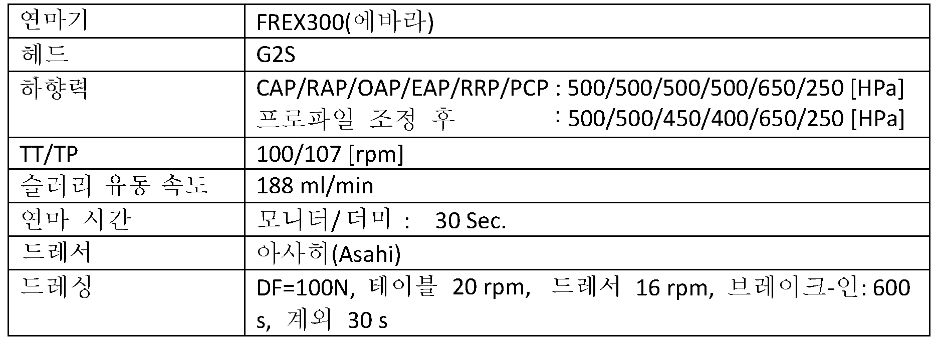
사용된 슬러리는 0.1 ㎛의 평균 입자 크기를 가지며 연마를 위한 사용 지점에서 DI 수를 사용하여 1:9 비율로 희석된 세리아 기재 슬러리였다. 에바라 테크놀로지스, 인크.(Ebara Technologies, Inc.)에 의한 300 mm CMP 연마 시스템 FREX300 상에서 연마를 수행하였다. 하기 표 2는 연마 조건을 요약한다.The slurry used was a ceria base slurry diluted 1: 9 with an average particle size of 0.1 [mu] m and using DI water at the point of use for polishing. Polishing was performed on a 300 mm CMP polishing system FREX300 by Ebara Technologies, Inc. Table 2 summarizes the polishing conditions.
<표 2><Table 2>
2가지 유형의 산화물 웨이퍼를 평가하였다. 이들은 화학 증착에 의해 형성된 TEOS 산화물 웨이퍼 (TEOS는 테트라에틸 오르소실리케이트의 분해 생성물을 나타냄) 및 열적으로 성장된 산화물 웨이퍼 (th-SiO2)였다. 2가지 유형의 산화물 웨이퍼의 제거 속도를 도 1에 나타내고 하기 표 3에 요약한다.Two types of oxide wafers were evaluated. These were TEOS oxide wafers (TEOS representing the decomposition products of tetraethylorthosilicate) formed by chemical vapor deposition and thermally grown oxide wafers (th-SiO 2 ). The removal rates of the two types of oxide wafers are shown in Figure 1 and summarized in Table 3 below.
<표 3><Table 3>

TEOS 산화물 웨이퍼에 대해, 상이한 슬러리 유동 속도에서 제거 속도를 또한 평가하였고, 결과를 도 2에 나타낸다. 105 퍼센트 화학량론을 갖는 연마 패드가 상이한 슬러리 유동 속도에서 일관성있게 더 높은 TEOS 제거 속도를 나타내었다.For TEOS oxide wafers, removal rates were also evaluated at different slurry flow rates, and the results are shown in FIG. Polishing pads with 105 percent stoichiometry showed consistently higher TEOS removal rates at different slurry flow rates.
TEOSTEOS 패턴화 웨이퍼 연마 Patterned wafer polishing
하기 표 4는 패턴 웨이퍼 연구에 사용된 연마 패드를 열거한다. 사용된 슬러리는 0.1 ㎛의 평균 입자 크기를 가지며 연마를 위한 사용 지점에서 DI 수를 사용하여 1:9 비율로 희석된 세리아 기재 슬러리였다. 모든 패드는 1.27 mm (50 mil) 천공된 연마 층 및 적층된 수바 400 서브패드를 가졌다. 패턴 웨이퍼 연구를 위한 연마 조건을 하기 표 5에 요약한다.Table 4 lists the polishing pads used in the patterned wafer study. The slurry used was a ceria base slurry diluted 1: 9 with an average particle size of 0.1 [mu] m and using DI water at the point of use for polishing. All pads had a 50 mil perforated abrasive layer and a stacked Suva 400 subpad. Polishing conditions for patterned wafer research are summarized in Table 5 below.
<표 4><Table 4>

<표 5><Table 5>

패턴 웨이퍼는 7000Å TEOS의 화학 증착에 의해 형성된 5000Å의 단 높이 (MIT-STI-764 패턴)를 가졌다. TEOS 침착 후에 패턴 웨이퍼의 단면을 도 3에 도시한다. 500 ㎛/500 ㎛ 및 25 ㎛/25 ㎛ 둘 다의 선/공간(L/S)에서 평탄화 효율을 평가하였다.The patterned wafer had a single height of 5000 angstroms (MIT-STI-764 pattern) formed by chemical vapor deposition of 7000 ANT TEOS. The cross section of the patterned wafer after TEOS deposition is shown in Fig. The planarization efficiency was evaluated in line / space (L / S) of both 500 탆 / 500 탆 and 25 탆 / 25 탆.
패드 1의 평탄화 효율은 대조 패드 A에 비해 우수한 것으로 밝혀졌고, 도 4 및 5에 나타낸 것과 같이 덜 다공성이고 더 경질의 대조 패드 C에 필적하였다. 더 빠른 단 높이 감소는 더 우수한 평탄화 효율을 나타낸다. 더욱이, 패드 1은 높은 제거 속도 및 우수한 평탄화 효율 둘 다를 가졌다. 그 결과, 이것은 도 6에 나타낸 것과 같이 평탄화를 달성함에 있어서 연마 시간을 현저하게 감소시킬 수 있다. 비율은 대조 패드 A에 비해 패드에 대한 연마 시간을 나타낸다. 비율이 낮을수록, 평탄화를 달성함에 있어서 패드가 더 효과적이다.The planarization efficiency of pad 1 was found to be superior to that of control pad A and was comparable to less porous and harder control pad C, as shown in FIGS. Faster height reduction results in better planarization efficiency. Furthermore, Pad 1 had both a high removal rate and excellent planarization efficiency. As a result, this can remarkably reduce the polishing time in achieving the planarization as shown in Fig. The ratio represents the polishing time for the pad as compared to the control pad A. The lower the ratio, the more effective the pad is in achieving planarization.
텅스텐 tungsten 블랭킷Blanket 웨이퍼 연마 Wafer polishing
어플라이드 머티어리얼스(Applied Materials)에 의해 제조된 미라(Mirra)TM 연마기에서 200 mm 웨이퍼로의 텅스텐 연마를 수행하였다. 캐보트(Cabot) SSW2000 텅스텐 슬러리로의 초기 평가를 위해 연마 조건을 하기에 요약한다. 상부 패드는 2.03 mm (80 mil) 두께이고, 1010 홈 및 1.02 mm (40 mil) 두께 수바TM IV 서브패드로 피니싱되었다.Tungsten polishing was performed on a 200 mm wafer from a Mirra TM polisher manufactured by Applied Materials. The polishing conditions for the initial evaluation of the Cabot SSW2000 tungsten slurry are summarized below. The top pad was 2.03 mm (80 mil) thick and was finished with 1010 grooves and a 1.02 mm (40 mil) thick Suba TM IV subpad.
텅스텐 200 mm 웨이퍼에 대한 연마 조건:Polishing conditions for tungsten 200 mm wafers:
슬러리: 캐보트 SSW2000 (2.0 중량% H2O2의 탈이온수를 사용하여 1:2 희석)Slurry: CABOT SSW 2000 (1: 2 dilution with deionized water of 2.0 wt% H 2 O 2 )
슬러리 유동 속도: 125 ml/minSlurry flow rate: 125 ml / min
슬러리 적하 지점: 중심으로부터 ~66 mmSlurry loading point: ~ 66 mm from center
조절장치: 새솔(Saesol) AM02BSL8031C1-PMControl device: Saesol AM02BSL8031C1-PM
패드 브레이크-인: 113/93 rpm, 3.2 Kg-f (7 lb-f) CDF, 10개의 총 영역, 3600초Pad break-in: 113/93 rpm, 3.2 Kg-f (7 lb-f) CDF, 10 total areas, 3600 seconds
계외 프로세스: 113/93 rpm, 3.2 Kg-f (7 lb-f), 10개의 총 영역, 10sOut-of-house process: 113/93 rpm, 3.2 Kg-f (7 lb-f), 10 total zones, 10 s
홈: 1010Home: 1010
연마 조건Abrasive condition
하향력: 29 kPa (4.2 psi)Downward force: 29 kPa (4.2 psi)
압반 속도: 113 rpmPlaten speed: 113 rpm
캐리어 속도: 111 rpmCarrier speed: 111 rpm
연마 시간: 60초Polishing time: 60 seconds
하기 표 6은 주요 패드 특성을 요약하고, DI 수 및 2.0 중량% H2O2로의 1:2 희석에서 캐보트 SSW2000 슬러리로의 텅스텐 제거 속도를 비교한다.Table 6 summarizes the key pad characteristics and compares the removal rates of tungsten to Cabot SSW2000 slurry at 1: 2 dilution with DI water and 2.0 wt% H 2 O 2 .
<표 6><Table 6>

105% 화학량론 및 33 부피 퍼센트의 세공을 갖는 4,4'-메틸렌비스(2-클로로아닐린) 경화제를 사용하여 경화된 H12MDI/TDI와 폴리테트라메틸렌 에테르 글리콜 연마 패드를 위한 연마 층을 갖는 패드 3에서, 텅스텐 제거 속도가 현저하게 더 높았다. 도 7은 상이한 연마 하향력에서 패드 3이 더 높은 텅스텐 제거 속도를 갖는 것을 나타낸다.A pad 3 with an abrasive layer for a polytetramethylene ether glycol polishing pad and H12MDI / TDI cured using 4,4'-methylene bis (2-chloroaniline) curing agent having 105% stoichiometry and 33 volume percent pores , The tungsten removal rate was significantly higher. Figure 7 shows that Pad 3 has a higher tungsten removal rate at different polishing down forces.
두번째 시험 시리즈에서, 상이한 희석 비율 (DI 수를 사용하여 1:1.5)의 캐보트 SSW2000 슬러리 및 개량된 텅스텐 슬러리를 또한 평가하였다. 연마 조건을 하기에 요약한다:In the second series of tests, Cabot SSW2000 slurries and modified tungsten slurries with different dilution ratios (1: 1.5 using DI water) were also evaluated. Polishing conditions are summarized below:
도구: 티탄(Titan) SP+ 헤드를 갖는 어플라이드 미라(Applied Mirra)Tool: Applied Mirra with Titan SP + head
슬러리 1: W2000 (1:1.5, 2.4 중량% H2O2), 70 ml/minSlurry 1: W2000 (1: 1.5, 2.4 wt% H 2 O 2 ), 70 ml / min
슬러리 2: 개량된 텅스텐 슬러리 (1:1.8, 2.0 중량% H2O2), 100 ml/minSlurry 2: Improved tungsten slurry (1: 1.8, 2.0 wt% H 2 O 2 ), 100 ml / min
컨디셔닝 디스크:Conditioning disc:
W2000 시험에 대해 키니크(Kinik) PDA32P-2N (IDG-2)For the W2000 test Kinik PDA32P-2N (IDG-2)
개량된 텅스텐 슬러리 시험에 대해 3M A3700For the modified tungsten slurry test 3M A3700
W2000을 사용한 레시피Recipe with W2000
패드 브레이크-인: 113/93 rpm, 5.0 Kg-f (11 lb-f) CDF, 10개의 총 영역, 30minPad break-in: 113/93 rpm, 5.0 Kg-f (11 lb-f) CDF, 10 total areas, 30 min
연마: 113/111 rpm, 29 kPa (4.2 psi), 60s, 70 ml/minPolishing: 113/111 rpm, 4.2 psi (29 kPa), 60s, 70 ml / min
컨디셔닝 : 계외: 113/93 rpm, 5.0 Kg-f (11 lb-f) CDF, 10개의 총 영역, 6sConditioning: Outside: 113/93 rpm, 5.0 Kg-f (11 lb-f) CDF, 10 total areas, 6 s
개량된 텅스텐 슬러리를 사용한 레시피Recipe with improved tungsten slurry
패드 브레이크-인: 80/36 rpm, 3.2 Kg-f (7 lb-f) CDF, 10개의 총 영역, 30minPad brake-in: 80/36 rpm, 3.2 Kg-f (7 lb-f) CDF, 10 total areas, 30 min
연마: 80/81 rpm, 21.4 kPa (3.1 psi), 100 ml/min, 60sPolishing: 80/81 rpm, 21.4 kPa (3.1 psi), 100 ml / min, 60 s
컨디셔닝 : 계외: 80/36 rpm, 3.2 Kg-f (7 lb-f) CDF, 10개의 총 영역, 24sConditioning: Off-the-shelf: 80/36 rpm, 3.2 Kg-f (7 lb-f) CDF, 10 total zones, 24s
모든 상부 패드는 2.03 mm (80 mil) 두께이고, 원형 K7 홈 및 1.02 mm (40 mil) 두께 수바 IV 서브패드로 피니싱되었다. 하기 표 7은 상이한 연마 패드의 주요 패드 특성, 텅스텐 제거 속도 및 최대 연마 온도를 요약한다. 텅스텐 제거 속도를 또한 도 8에 나타낸다. 다시, 본 발명으로부터의 연마 패드는 상당히 높은 제거 속도를 나타내었다.All top pads were 2.03 mm (80 mils) thick and were finished with a round K7 groove and a 1.02 mm (40 mil) thick Suva IV subpad. Table 7 below summarizes the main pad properties, tungsten removal rate and maximum polishing temperature of different polishing pads. The tungsten removal rate is also shown in FIG. Again, the polishing pad from the present invention exhibited a significantly higher removal rate.
<표 7><Table 7>

*= 개량된 텅스텐 슬러리* = Improved tungsten slurry
NA= 이용가능하지 않음NA = not available
최대 온도는 연마 동안에 달성된 최대 온도를 나타낸다.The maximum temperature represents the maximum temperature achieved during polishing.
물리적 특성Physical Characteristics
행렬 물리적 특성 데이터는 105% 화학량론에서 4,4'-메틸렌비스(2-클로로아닐린)을 사용하여 경화된 H12MDI/TDI와 폴리테트라메틸렌 에테르 글리콜에 대한 임계 범위를 증명한다. 약 87% 내지 115% 범위의 화학량론으로 실험실에서 비충전 샘플을 제조하였다. 경도 측정을 ASTM-D2240에 따라 수행하여, D 팁을 갖는 쇼어 S1, 모델 902 측정 도구를 사용하여 2초에서, 이어서 다시 15초에서 쇼어 D 경도를 측정하였다. 이어서, 전단 저장 탄성률 및 전단 손실 탄성률을 10 rad/s 진동수 및 -100℃로부터 150℃까지의 3℃/min 온도 경사에서 비틀림 고정구로 측정하였다 (ASTM D5279). 전단 탄성률 샘플은 6.5 mm의 폭, 1.26 내지 2.0 mm의 두께 및 20 mm의 간극 길이를 가졌다. 중앙 인장 탄성률 (ASTM-D412)에 대한 시험 방법을, 하기와 같은 기하구조를 갖는 5개의 시편으로부터 측정하였다: 4.5 인치 (11.4 cm)의 총 길이, 0.75 인치 (0.19 cm)의 총 폭, 1.5 인치 (3.8 cm)의 목부 길이 및 0.25 인치 (0.6 cm)의 목부 폭을 갖는 덤벨 형상. 1.5 인치 (목부에 대해 3.81 cm)의 소프트웨어에 입력된 공칭 게이지 길이와 함께 그립 분리는 2.5 인치 (6.35 cm)이고, 크로스헤드 속도는 20 인치/min (50.8 cm/min)의 속도였다.Matrix physical property data demonstrate critical ranges for H12MDI / TDI and polytetramethylene ether glycol cured using 4,4'-methylene bis (2-chloroaniline) at 105% stoichiometry. Unfilled samples were prepared in the laboratory with stoichiometries ranging from about 87% to 115%. Hardness measurements were made according to ASTM-D2240 and Shore D hardness was measured at 2 seconds using a Shore S1, Model 902 measuring tool with a D tip, followed by another 15 seconds. The shear storage modulus and shear loss modulus were then measured with a torsion fixture at a frequency of 10 rad / s and a temperature gradient of 3 DEG C / min from -100 DEG C to 150 DEG C (ASTM D5279). The shear modulus samples had a width of 6.5 mm, a thickness of 1.26 to 2.0 mm and a gap length of 20 mm. The test method for the central tensile modulus (ASTM-D412) was measured from five specimens having geometries as follows: a total length of 4.5 inches (11.4 cm), a total width of 0.75 inches (0.19 cm) (3.8 cm) neck length and 0.25 inch (0.6 cm) neck width. The grip separation was 2.5 inches (6.35 cm) with a nominal gage length entered into the software at 1.5 inches (3.81 cm for the neck) and the crosshead speed was 20 inches / min (50.8 cm / min).
물리적 특성을 하기 표 8 및 9에 요약한다.Physical properties are summarized in Tables 8 and 9 below.
<표 8><Table 8>

<표 9><Table 9>

요약하면, 배합물, 전단 저장 탄성률, 전단 손실 탄성률 및 기공률의 특정 조합은 텅스텐 및 TEOS 연마 특징을 제공한다. 더욱이, 이러한 연마 패드는 TEOS 시트 웨이퍼 연마에 있어서 현행 산업 표준 IC1000 또는 VP5000 연마 패드보다 현저하게 더 높은 제거 속도를 나타내었다.In summary, certain combinations of formulations, shear storage modulus, shear loss modulus, and porosity provide tungsten and TEOS polishing characteristics. Moreover, these polishing pads exhibited significantly higher removal rates in the TEOS sheet wafer polishing than current industry standard IC1000 or VP5000 polishing pads.
Claims (10)
Applications Claiming Priority (2)
| Application Number | Priority Date | Filing Date | Title |
|---|---|---|---|
| US14/465,934 | 2014-08-22 | ||
| US14/465,934 US9731398B2 (en) | 2014-08-22 | 2014-08-22 | Polyurethane polishing pad |
Publications (2)
| Publication Number | Publication Date |
|---|---|
| KR20160023575A true KR20160023575A (en) | 2016-03-03 |
| KR102456044B1 KR102456044B1 (en) | 2022-10-19 |
Family
ID=55273973
Family Applications (1)
| Application Number | Title | Priority Date | Filing Date |
|---|---|---|---|
| KR1020150116435A KR102456044B1 (en) | 2014-08-22 | 2015-08-19 | Polyurethane polishing pad |
Country Status (7)
| Country | Link |
|---|---|
| US (1) | US9731398B2 (en) |
| JP (1) | JP6625368B2 (en) |
| KR (1) | KR102456044B1 (en) |
| CN (1) | CN105382680B (en) |
| DE (1) | DE102015009512A1 (en) |
| FR (1) | FR3024955B1 (en) |
| TW (1) | TWI589613B (en) |
Families Citing this family (22)
| Publication number | Priority date | Publication date | Assignee | Title |
|---|---|---|---|---|
| US9873180B2 (en) | 2014-10-17 | 2018-01-23 | Applied Materials, Inc. | CMP pad construction with composite material properties using additive manufacturing processes |
| US11745302B2 (en) | 2014-10-17 | 2023-09-05 | Applied Materials, Inc. | Methods and precursor formulations for forming advanced polishing pads by use of an additive manufacturing process |
| US10875145B2 (en) | 2014-10-17 | 2020-12-29 | Applied Materials, Inc. | Polishing pads produced by an additive manufacturing process |
| KR20240015167A (en) | 2014-10-17 | 2024-02-02 | 어플라이드 머티어리얼스, 인코포레이티드 | Cmp pad construction with composite material properties using additive manufacturing processes |
| US10875153B2 (en) | 2014-10-17 | 2020-12-29 | Applied Materials, Inc. | Advanced polishing pad materials and formulations |
| US10399201B2 (en) | 2014-10-17 | 2019-09-03 | Applied Materials, Inc. | Advanced polishing pads having compositional gradients by use of an additive manufacturing process |
| US10821573B2 (en) | 2014-10-17 | 2020-11-03 | Applied Materials, Inc. | Polishing pads produced by an additive manufacturing process |
| US10391605B2 (en) | 2016-01-19 | 2019-08-27 | Applied Materials, Inc. | Method and apparatus for forming porous advanced polishing pads using an additive manufacturing process |
| US10456886B2 (en) | 2016-01-19 | 2019-10-29 | Applied Materials, Inc. | Porous chemical mechanical polishing pads |
| US10086494B2 (en) * | 2016-09-13 | 2018-10-02 | Rohm And Haas Electronic Materials Cmp Holdings, Inc. | High planarization efficiency chemical mechanical polishing pads and methods of making |
| US10181408B2 (en) * | 2017-01-31 | 2019-01-15 | Rohm And Haas Electronic Materials Cmp Holdings, Inc. | Chemical mechanical polishing method for tungsten using polyglycols and polyglycol derivatives |
| US20180304539A1 (en) | 2017-04-21 | 2018-10-25 | Applied Materials, Inc. | Energy delivery system with array of energy sources for an additive manufacturing apparatus |
| US11471999B2 (en) | 2017-07-26 | 2022-10-18 | Applied Materials, Inc. | Integrated abrasive polishing pads and manufacturing methods |
| US11072050B2 (en) | 2017-08-04 | 2021-07-27 | Applied Materials, Inc. | Polishing pad with window and manufacturing methods thereof |
| WO2019032286A1 (en) | 2017-08-07 | 2019-02-14 | Applied Materials, Inc. | Abrasive delivery polishing pads and manufacturing methods thereof |
| US10600655B2 (en) * | 2017-08-10 | 2020-03-24 | Rohm And Haas Electronic Materials Cmp Holdings, Inc. | Chemical mechanical polishing method for tungsten |
| WO2019042428A1 (en) * | 2017-08-31 | 2019-03-07 | 湖北鼎汇微电子材料有限公司 | Polyurethane polishing layer, polishing pad containing polishing layer, method for preparing polishing layer and method for planarizing material |
| JP7259311B2 (en) * | 2017-12-26 | 2023-04-18 | Dic株式会社 | Polishing pad and urethane resin composition for polishing pad |
| CN112654655A (en) | 2018-09-04 | 2021-04-13 | 应用材料公司 | Advanced polishing pad formulations |
| US11813712B2 (en) | 2019-12-20 | 2023-11-14 | Applied Materials, Inc. | Polishing pads having selectively arranged porosity |
| US11806829B2 (en) | 2020-06-19 | 2023-11-07 | Applied Materials, Inc. | Advanced polishing pads and related polishing pad manufacturing methods |
| US11878389B2 (en) | 2021-02-10 | 2024-01-23 | Applied Materials, Inc. | Structures formed using an additive manufacturing process for regenerating surface texture in situ |
Citations (2)
| Publication number | Priority date | Publication date | Assignee | Title |
|---|---|---|---|---|
| JP2007520617A (en) * | 2004-02-03 | 2007-07-26 | ローム アンド ハース エレクトロニック マテリアルズ シーエムピー ホウルディングス インコーポレイテッド | Polyurethane polishing pad |
| KR100877383B1 (en) * | 2001-11-13 | 2009-01-07 | 도요 고무 고교 가부시키가이샤 | Grinding pad and method of producing the same |
Family Cites Families (12)
| Publication number | Priority date | Publication date | Assignee | Title |
|---|---|---|---|---|
| MY114512A (en) | 1992-08-19 | 2002-11-30 | Rodel Inc | Polymeric substrate with polymeric microelements |
| KR100574311B1 (en) * | 1998-08-28 | 2006-04-27 | 도레이 가부시끼가이샤 | Polishing Pad |
| EP1284841B1 (en) | 2000-05-27 | 2005-03-23 | Rohm and Haas Electronic Materials CMP Holdings, Inc. | Grooved polishing pads for chemical mechanical planarization |
| JP3455208B2 (en) * | 2001-11-13 | 2003-10-14 | 東洋紡績株式会社 | Semiconductor wafer polishing pad, method for polishing semiconductor wafer, polishing sheet for polishing pad, and foam block for polishing sheet |
| CN1318469C (en) * | 2002-11-18 | 2007-05-30 | 东省A&T株式会社 | Method of fabricating polyurethane foam with micro pores and polishing pad therefrom |
| SG111222A1 (en) * | 2003-10-09 | 2005-05-30 | Rohm & Haas Elect Mat | Polishing pad |
| TWI372108B (en) * | 2005-04-06 | 2012-09-11 | Rohm & Haas Elect Mat | Method for forming a porous reaction injection molded chemical mechanical polishing pad |
| US7169030B1 (en) | 2006-05-25 | 2007-01-30 | Rohm And Haas Electronic Materials Cmp Holdings, Inc. | Chemical mechanical polishing pad |
| US20090062414A1 (en) * | 2007-08-28 | 2009-03-05 | David Picheng Huang | System and method for producing damping polyurethane CMP pads |
| KR101186531B1 (en) * | 2009-03-24 | 2012-10-08 | 차윤종 | Polyurethane porous product and manufacturing method thereof and Polishing pad having Polyurethane porous product |
| JP5715770B2 (en) * | 2010-06-17 | 2015-05-13 | ローム アンド ハース エレクトロニック マテリアルズ シーエムピー ホウルディングス インコーポレイテッド | Chemical mechanical polishing pad having a low defect integral window and method of chemical mechanical polishing a substrate using the chemical mechanical polishing pad |
| US8257152B2 (en) * | 2010-11-12 | 2012-09-04 | Rohm And Haas Electronic Materials Cmp Holdings, Inc. | Silicate composite polishing pad |
-
2014
- 2014-08-22 US US14/465,934 patent/US9731398B2/en active Active
-
2015
- 2015-07-23 DE DE102015009512.9A patent/DE102015009512A1/en not_active Withdrawn
- 2015-08-04 TW TW104125197A patent/TWI589613B/en active
- 2015-08-19 KR KR1020150116435A patent/KR102456044B1/en active IP Right Grant
- 2015-08-19 FR FR1557800A patent/FR3024955B1/en active Active
- 2015-08-19 CN CN201510512498.4A patent/CN105382680B/en active Active
- 2015-08-20 JP JP2015162800A patent/JP6625368B2/en active Active
Patent Citations (2)
| Publication number | Priority date | Publication date | Assignee | Title |
|---|---|---|---|---|
| KR100877383B1 (en) * | 2001-11-13 | 2009-01-07 | 도요 고무 고교 가부시키가이샤 | Grinding pad and method of producing the same |
| JP2007520617A (en) * | 2004-02-03 | 2007-07-26 | ローム アンド ハース エレクトロニック マテリアルズ シーエムピー ホウルディングス インコーポレイテッド | Polyurethane polishing pad |
Also Published As
| Publication number | Publication date |
|---|---|
| US9731398B2 (en) | 2017-08-15 |
| KR102456044B1 (en) | 2022-10-19 |
| CN105382680A (en) | 2016-03-09 |
| CN105382680B (en) | 2020-02-28 |
| JP2016043479A (en) | 2016-04-04 |
| TW201615342A (en) | 2016-05-01 |
| US20160052103A1 (en) | 2016-02-25 |
| DE102015009512A1 (en) | 2016-02-25 |
| JP6625368B2 (en) | 2019-12-25 |
| TWI589613B (en) | 2017-07-01 |
| FR3024955B1 (en) | 2019-12-06 |
| FR3024955A1 (en) | 2016-02-26 |
Similar Documents
| Publication | Publication Date | Title |
|---|---|---|
| KR102456044B1 (en) | Polyurethane polishing pad | |
| US7414080B2 (en) | Polyurethane polishing pad | |
| JP5346445B2 (en) | Chemical mechanical polishing pad | |
| US8697239B2 (en) | Multi-functional polishing pad | |
| US7074115B2 (en) | Polishing pad | |
| KR101526010B1 (en) | Chemical mechanical polishing pad | |
| EP2151299B1 (en) | Chemical mechanical polishing pad | |
| JP6423205B2 (en) | Polyurethane polishing pad | |
| US9586304B2 (en) | Controlled-expansion CMP PAD casting method | |
| US9452507B2 (en) | Controlled-viscosity CMP casting method | |
| EP1522385B1 (en) | Polishing Pad | |
| US9481070B2 (en) | High-stability polyurethane polishing pad |
Legal Events
| Date | Code | Title | Description |
|---|---|---|---|
| A201 | Request for examination | ||
| E902 | Notification of reason for refusal | ||
| E701 | Decision to grant or registration of patent right |