KR20160017841A - Led driving device and lighting device - Google Patents
Led driving device and lighting device Download PDFInfo
- Publication number
- KR20160017841A KR20160017841A KR1020140101115A KR20140101115A KR20160017841A KR 20160017841 A KR20160017841 A KR 20160017841A KR 1020140101115 A KR1020140101115 A KR 1020140101115A KR 20140101115 A KR20140101115 A KR 20140101115A KR 20160017841 A KR20160017841 A KR 20160017841A
- Authority
- KR
- South Korea
- Prior art keywords
- voltage
- circuit
- input voltage
- driving
- led
- Prior art date
- Legal status (The legal status is an assumption and is not a legal conclusion. Google has not performed a legal analysis and makes no representation as to the accuracy of the status listed.)
- Withdrawn
Links
Images


Classifications
-
- H—ELECTRICITY
- H05—ELECTRIC TECHNIQUES NOT OTHERWISE PROVIDED FOR
- H05B—ELECTRIC HEATING; ELECTRIC LIGHT SOURCES NOT OTHERWISE PROVIDED FOR; CIRCUIT ARRANGEMENTS FOR ELECTRIC LIGHT SOURCES, IN GENERAL
- H05B47/00—Circuit arrangements for operating light sources in general, i.e. where the type of light source is not relevant
- H05B47/10—Controlling the light source
-
- H—ELECTRICITY
- H05—ELECTRIC TECHNIQUES NOT OTHERWISE PROVIDED FOR
- H05B—ELECTRIC HEATING; ELECTRIC LIGHT SOURCES NOT OTHERWISE PROVIDED FOR; CIRCUIT ARRANGEMENTS FOR ELECTRIC LIGHT SOURCES, IN GENERAL
- H05B45/00—Circuit arrangements for operating light-emitting diodes [LED]
- H05B45/50—Circuit arrangements for operating light-emitting diodes [LED] responsive to malfunctions or undesirable behaviour of LEDs; responsive to LED life; Protective circuits
-
- F—MECHANICAL ENGINEERING; LIGHTING; HEATING; WEAPONS; BLASTING
- F21—LIGHTING
- F21V—FUNCTIONAL FEATURES OR DETAILS OF LIGHTING DEVICES OR SYSTEMS THEREOF; STRUCTURAL COMBINATIONS OF LIGHTING DEVICES WITH OTHER ARTICLES, NOT OTHERWISE PROVIDED FOR
- F21V25/00—Safety devices structurally associated with lighting devices
-
- H—ELECTRICITY
- H05—ELECTRIC TECHNIQUES NOT OTHERWISE PROVIDED FOR
- H05B—ELECTRIC HEATING; ELECTRIC LIGHT SOURCES NOT OTHERWISE PROVIDED FOR; CIRCUIT ARRANGEMENTS FOR ELECTRIC LIGHT SOURCES, IN GENERAL
- H05B45/00—Circuit arrangements for operating light-emitting diodes [LED]
- H05B45/10—Controlling the intensity of the light
-
- H—ELECTRICITY
- H05—ELECTRIC TECHNIQUES NOT OTHERWISE PROVIDED FOR
- H05B—ELECTRIC HEATING; ELECTRIC LIGHT SOURCES NOT OTHERWISE PROVIDED FOR; CIRCUIT ARRANGEMENTS FOR ELECTRIC LIGHT SOURCES, IN GENERAL
- H05B45/00—Circuit arrangements for operating light-emitting diodes [LED]
- H05B45/30—Driver circuits
- H05B45/37—Converter circuits
- H05B45/3725—Switched mode power supply [SMPS]
- H05B45/38—Switched mode power supply [SMPS] using boost topology
-
- H—ELECTRICITY
- H05—ELECTRIC TECHNIQUES NOT OTHERWISE PROVIDED FOR
- H05B—ELECTRIC HEATING; ELECTRIC LIGHT SOURCES NOT OTHERWISE PROVIDED FOR; CIRCUIT ARRANGEMENTS FOR ELECTRIC LIGHT SOURCES, IN GENERAL
- H05B45/00—Circuit arrangements for operating light-emitting diodes [LED]
- H05B45/30—Driver circuits
- H05B45/37—Converter circuits
- H05B45/3725—Switched mode power supply [SMPS]
- H05B45/375—Switched mode power supply [SMPS] using buck topology
-
- Y—GENERAL TAGGING OF NEW TECHNOLOGICAL DEVELOPMENTS; GENERAL TAGGING OF CROSS-SECTIONAL TECHNOLOGIES SPANNING OVER SEVERAL SECTIONS OF THE IPC; TECHNICAL SUBJECTS COVERED BY FORMER USPC CROSS-REFERENCE ART COLLECTIONS [XRACs] AND DIGESTS
- Y02—TECHNOLOGIES OR APPLICATIONS FOR MITIGATION OR ADAPTATION AGAINST CLIMATE CHANGE
- Y02B—CLIMATE CHANGE MITIGATION TECHNOLOGIES RELATED TO BUILDINGS, e.g. HOUSING, HOUSE APPLIANCES OR RELATED END-USER APPLICATIONS
- Y02B20/00—Energy efficient lighting technologies, e.g. halogen lamps or gas discharge lamps
- Y02B20/30—Semiconductor lamps, e.g. solid state lamps [SSL] light emitting diodes [LED] or organic LED [OLED]
Landscapes
- Engineering & Computer Science (AREA)
- General Engineering & Computer Science (AREA)
- Circuit Arrangement For Electric Light Sources In General (AREA)
Abstract
본 발명의 실시 형태에 따른 LED 구동 장치는, 입력 전압을 이용하여 복수의 LED를 구동하기 위한 구동 전류를 출력하는 구동 회로, 상기 입력 전압을 검출하여 센싱 전압을 출력하며, 상기 입력 전압이 증가하여 소정의 기준 전압보다 커지거나 상기 입력 전압이 감소하여 상기 기준 전압보다 작아질 때 히스테리시스 특성을 갖고 동작하는 회로 소자를 포함하는 보호 회로, 및 상기 센싱 전압 및 상기 구동 전류를 검출하여 상기 구동 회로의 동작을 제어하는 제어 회로를 포함한다.An LED driving apparatus according to an embodiment of the present invention includes a driving circuit for outputting a driving current for driving a plurality of LEDs using an input voltage, a detecting circuit for detecting the input voltage and outputting a sensing voltage, A protection circuit including a circuit element that operates with a hysteresis characteristic when the input voltage is lower than the predetermined reference voltage or when the input voltage is decreased to be smaller than the reference voltage, And a control circuit for controlling the control circuit.
Description
본 발명은 LED 구동 장치 및 조명 장치에 관한 것이다.
The present invention relates to an LED driving apparatus and a lighting apparatus.
발광 다이오드(Light Emitting Diode, LED)는 낮은 소비전력, 고휘도 등의 여러 장점 때문에 광원으로서 널리 사용된다. 특히 최근 발광 다이오드는 디스플레이용 백라이트 유닛과 자동차용 헤드 램프를 포함하는 다양한 발광 장치에 채용되고 있다. 이러한 발광소자는 각종 장치에 장착되기 용이한 패키지형태로 제공된다. 발광 다이오드는 정전류 제어에 의해 동작하므로, 안정적으로 발광 다이오드를 동작하기 위해서는 입력 전압의 변화에 대해 정전류를 안정적으로 출력할 수 있는 구동 장치가 필요하다.
Light emitting diodes (LEDs) are widely used as light sources because of their low power consumption and high brightness. In particular, recently, light emitting diodes have been employed in various light emitting devices including a backlight unit for a display and a head lamp for an automobile. Such a light emitting element is provided in the form of a package easy to be mounted on various apparatuses. Since the light emitting diode operates by the constant current control, a driving device capable of stably outputting the constant current with respect to the change of the input voltage is required in order to stably operate the light emitting diode.
당 기술분야에서는, 발광 다이오드의 동작에 필요한 최소 전압의 경계 대역에서 입력 전압이 변화하는 경우, 안정적으로 발광 다이오드를 동작시킬 수 있는 LED 구동 장치가 요구되고 있다.
In the related art, there is a demand for an LED driving apparatus capable of stably operating a light emitting diode when an input voltage changes in a boundary band of a minimum voltage required for operation of the light emitting diode.
본 발명의 일 실시 형태에 따른 LED 구동 장치는, 입력 전압을 이용하여 복수의 LED를 구동하기 위한 구동 전류를 출력하는 구동 회로; 상기 입력 전압을 검출하여 센싱 전압을 출력하며, 상기 입력 전압이 증가하여 소정의 기준 전압보다 커지거나 상기 입력 전압이 감소하여 상기 기준 전압보다 작아질 때 히스테리시스 특성을 갖고 동작하는 회로 소자를 포함하는 보호 회로; 및 상기 센싱 전압 및 상기 구동 전류를 검출하여 상기 구동 회로의 동작을 제어하는 제어 회로; 를 포함한다.An LED driving apparatus according to an embodiment of the present invention includes a driving circuit for outputting a driving current for driving a plurality of LEDs using an input voltage; And a circuit element which operates with a hysteresis characteristic when the input voltage increases and becomes greater than a predetermined reference voltage or when the input voltage decreases and becomes smaller than the reference voltage by detecting the input voltage and outputting a sensing voltage. Circuit; And a control circuit for detecting the sensing voltage and the driving current to control the operation of the driving circuit. .
본 발명의 일부 실시 형태에서, 상기 보호 회로는, 상기 입력 전압이 증가하여 소정의 기준 전압보다 커지면, 상기 회로 소자를 턴-온시켜 상기 센싱 전압을 감소시킬 수 있다.In some embodiments of the present invention, the protection circuit may reduce the sensing voltage by turning on the circuit element when the input voltage increases and becomes greater than a predetermined reference voltage.
본 발명의 일부 실시 형태에서, 상기 제어 회로는, 상기 센싱 전압이 소정의 임계 전압보다 작아지면, 상기 구동 회로가 상기 구동 전류를 출력하도록 제어할 수 있다.In some embodiments of the present invention, the control circuit may control the drive circuit to output the drive current when the sensing voltage becomes smaller than a predetermined threshold voltage.
본 발명의 일부 실시 형태에서, 상기 구동 회로는 상기 복수의 LED를 구동하기 위한 정전류를 생성하는 부스트 컨버터, 벅 컨버터 중 적어도 하나를 포함하며, 상기 제어 회로는 상기 부스트 컨버터, 상기 벅 컨버터 중 적어도 하나에 포함되는 스위치 소자의 동작을 제어할 수 있다.In some embodiments of the present invention, the driving circuit includes at least one of a boost converter and a buck converter that generates a constant current for driving the plurality of LEDs, and the control circuit controls at least one of the boost converter, It is possible to control the operation of the switch element included in the switch element.
본 발명의 일부 실시 형태에서, 상기 제어 회로는 상기 센싱 전압을 아날로그 디밍 신호로 이용하여 상기 스위치 소자의 동작을 제어할 수 있다.In some embodiments of the present invention, the control circuit can use the sensing voltage as an analog dimming signal to control the operation of the switch element.
본 발명의 일부 실시 형태에서, 상기 보호 회로는, 상기 입력 전압이 감소하면, 상기 센싱 전압을 상기 입력 전압의 감소량보다 크게 감소시킬 수 있다.In some embodiments of the present invention, the protection circuit may reduce the sensing voltage to greater than the reduction amount of the input voltage when the input voltage is decreased.
본 발명의 일부 실시 형태에서, 상기 제어 회로는, 상기 입력 전압이 감소하면, 상기 센싱 전압의 감소량을 반영하여 상기 구동 전류가 감소하도록 상기 구동 회로를 제어할 수 있다.
In some embodiments of the present invention, the control circuit may control the driving circuit so that the driving current is reduced by reflecting a reduction amount of the sensing voltage when the input voltage is decreased.
본 발명의 일부 실시 형태에 따른 조명 장치는, 복수의 LED를 포함하는 광원부; 및 직류 입력 전압을 검출하여 센싱 전압을 생성하는 보호 회로와, 상기 센싱 전압에 기초하여 상기 복수의 LED를 동작하는 구동 전류를 출력하는 구동 회로를 갖는 LED 구동부; 를 포함하며, 상기 보호 회로는 상기 직류 입력 전압이 차단되면, 상기 직류 입력 전압의 감소량보다 상기 센싱 전압을 크게 감소시키며, 상기 LED 구동부는 상기 센싱 전압의 감소량에 기초하여 상기 구동 전류를 감소시킨다.An illumination device according to some embodiments of the present invention includes: a light source unit including a plurality of LEDs; And a driving circuit for outputting a driving current for operating the plurality of LEDs based on the sensing voltage. Wherein the protection circuit greatly reduces the sensing voltage when the DC input voltage is cut off, the sensing voltage being lower than the reduction amount of the DC input voltage, and the LED driver reduces the driving current based on the reduction amount of the sensing voltage.
본 발명의 일부 실시 형태에서, 상기 보호 회로는, 상기 입력 전압이 증가하여 소정의 기준 전압보다 커지면, 소정의 지연 시간이 경과한 후에 상기 센싱 전압이 소정의 임계 전압보다 작아지도록 상기 센싱 전압을 감소시킬 수 있다.
In some embodiments of the present invention, the protection circuit decreases the sensing voltage so that the sensing voltage becomes smaller than a predetermined threshold voltage after a predetermined delay time elapses when the input voltage increases and becomes greater than a predetermined reference voltage .
본 발명에 따르면, 히스테리시스 특성을 갖는 보호 회로를 이용하여 입력 전압으로부터 센싱 전압을 생성하고, 구동 회로는 센싱 전압과 LED에 인가되는 구동 전류를 검출하여 구동 전류를 조절할 수 있다. 보호 회로의 히스테리시스 특성에 의해 입력 전압이 LED를 구동할 수 있는 최소한의 기준 전압 부근에서 구동 회로의 동작이 일정 시간만큼 지연되므로, 입력 전압이 기준 전압 부근의 값을 가질 때 발생할 수 있는 LED의 채터링(chattering) 등을 방지할 수 있으며, 전원이 차단되어 입력 전압이 감소하는 조건에서 구동 회로와 LED 등에 가해질 수 있는 과도한 스트레스를 방지할 수 있다.According to the present invention, a sensing voltage is generated from an input voltage using a protection circuit having a hysteresis characteristic, and the driving circuit can control a driving current by detecting a sensing voltage and a driving current applied to the LED. The operation of the driving circuit is delayed by a predetermined time in the vicinity of the minimum reference voltage at which the input voltage can drive the LED due to the hysteresis characteristic of the protection circuit. Therefore, when the input voltage has a value near the reference voltage, Chattering and the like can be prevented and excessive stress that may be applied to the driving circuit and the LED can be prevented under the condition that the power supply is cut off and the input voltage is reduced.
본 발명의 다양하면서도 유익한 장점과 효과는 상술한 내용에 한정되지 않으며, 본 발명의 구체적인 실시형태를 설명하는 과정에서 보다 쉽게 이해될 수 있을 것이다.
The various and advantageous advantages and effects of the present invention are not limited to the above description, and can be more easily understood in the course of describing a specific embodiment of the present invention.
도 1은 본 발명의 일 실시 형태에 따른 조명 장치를 개략적으로 도시하는 블록도이다.
도 2는 본 발명의 일 실시 형태에 따른 LED 구동 장치를 개략적으로 도시하는 블록도이다.
도 3은 도 2의 LED 구동 장치에 채용될 수 있는 구동 회로의 일 실시 형태를 대략적으로 나타낸 회로도이다.
도 4는 도 2의 LED 구동 장치에 채용될 수 있는 보호 회로의 일 실시 형태를 대략적으로 나타낸 회로도이다.
도 5는 본 발명의 일 실시 형태에 따른 LED 구동 장치를 나타낸 회로도이다.
도 6은 도 4에 도시한 보호 회로의 동작을 설명하기 위한 그래프이다.
도 7은 도 5에 도시한 LED 구동 장치의 동작을 설명하기 위한 그래프이다.
도 8 및 도 9는 본 발명의 일 실시 형태에 따른 조명 장치에 적용될 수 있는 LED 패키지를 나타낸 것이다.
도 10은 본 발명의 일 실시 형태에 따른 조명 장치를 나타낸 도이다.1 is a block diagram schematically showing a lighting apparatus according to an embodiment of the present invention.
2 is a block diagram schematically showing an LED driving apparatus according to an embodiment of the present invention.
Fig. 3 is a circuit diagram schematically showing an embodiment of a driving circuit that can be employed in the LED driving apparatus of Fig. 2; Fig.
4 is a circuit diagram schematically showing one embodiment of a protection circuit that can be employed in the LED driving apparatus of Fig.
5 is a circuit diagram showing an LED driving apparatus according to an embodiment of the present invention.
6 is a graph for explaining the operation of the protection circuit shown in FIG.
7 is a graph for explaining the operation of the LED driving apparatus shown in FIG.
8 and 9 show an LED package that can be applied to a lighting device according to an embodiment of the present invention.
10 is a diagram showing a lighting apparatus according to an embodiment of the present invention.
이하, 첨부된 도면을 참조하여 본 발명의 바람직한 실시 형태들을 다음과 같이 설명한다.Hereinafter, preferred embodiments of the present invention will be described with reference to the accompanying drawings.
본 발명의 실시 형태는 여러 가지 다른 형태로 변형되거나 여러 가지 실시 형태가 조합될 수 있으며, 본 발명의 범위가 이하 설명하는 실시 형태로 한정되는 것은 아니다. 또한, 본 발명의 실시 형태는 당해 기술분야에서 평균적인 지식을 가진 자에게 본 발명을 더욱 완전하게 설명하기 위해서 제공되는 것이다. 따라서, 도면에서의 요소들의 형상 및 크기 등은 보다 명확한 설명을 위해 과장될 수 있으며, 도면 상의 동일한 부호로 표시되는 요소는 동일한 요소이다.
The embodiments of the present invention may be modified into various other forms or various embodiments may be combined, and the scope of the present invention is not limited to the embodiments described below. Further, the embodiments of the present invention are provided to more fully explain the present invention to those skilled in the art. Accordingly, the shapes and sizes of the elements in the drawings may be exaggerated for clarity of description, and the elements denoted by the same reference numerals in the drawings are the same elements.
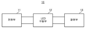
도 1은 본 발명의 일 실시 형태에 따른 조명 장치를 개략적으로 도시하는 블록도이다.1 is a block diagram schematically showing a lighting apparatus according to an embodiment of the present invention.
도 1을 참조하면, 본 발명의 일 실시 형태에 따른 조명 장치(10)는 전원부(11), LED 구동부(12), 및 광원부(13)를 포함할 수 있다. 전원부(11)는 광원부(13)가 동작하는 데에 필요한 입력 전압을 생성할 수 있으며, 상기 입력 전압은 직류 특성을 가질 수 있다. 조명 장치(10)가 자동차용 헤드램프인 경우, 전원부(11)는 자동차에 탑재된 배터리를 포함할 수 있다. 또한, 조명 장치(10)가 가정용, 사업용 조명기구인 경우, 전원부(11)는 교류 전압을 생성하는 교류 전원 및 교류 전압을 정류하여 직류 전압을 생성하는 정류회로와 전압 레귤레이터 회로 등을 포함할 수 있다. Referring to FIG. 1, a
LED 구동부(12)는 전원부(11)가 생성한 입력 전압을 이용하여 광원부(13)에 포함되는 하나 이상의 LED를 구동할 수 있다. LED 구동부(12)는 LED를 구동할 수 있는 LED 전류를 생성하는 구동 회로를 가질 수 있으며, 구동 회로는 DC-DC 컨버터 회로를 포함할 수 있다. 일 실시예로, 조명 장치(10)가 자동차용 헤드램프인 경우, LED 구동부(12)는 부스트 컨버터를 포함할 수 있으며, 조명 장치(10)가 가정용, 사업용 조명기구인 경우 LED 구동부(12)는 벅 컨버터를 포함할 수 있다. LED 구동부(12)는 구동 회로에 포함되는 스위치 소자의 동작을 제어하기 위한 제어 회로를 포함할 수 있다. 제어 회로는 LED 구동부에 포함되는 부스트 컨버터, 벅 컨버터 등의 DC-DC 컨버터의 동작을, PWM 디밍 또는 아날로그 디밍 방식에 의해 제어할 수 있다.The
LED 구동부(12)는 전원부(11)가 출력하는 직류 전압 및 광원부(13)에 인가되는 LED 전류를 검출할 수 있으며, 검출 결과에 기초하여 광원부(13)에 인가되는 LED 전류를 조절할 수 있다. 직류 전압이 LED 구동에 필요한 기준 전압보다 작은 경우 LED 구동부(12)는 동작하지 않을 수 있으며, LED 구동에 필요한 기준 전압 이상으로 상승할 때 LED 구동부(12)는 광원부(13)에 전류를 공급할 수 있다. 또한, 광원부(13)에 포함되는 LED에 인가되는 스트레스를 줄이고 LED의 수명 단축을 막기 위해 입력 전압 및 LED 전류를 검출하고 그 결과를 이용하여 LED 전류를 조절할 수 있다. 즉, 광원부(13)에 인가되는 LED 전류는, LED 구동부(12)가 검출하는 입력 전압 및 LED 전류에 의해 결정될 수 있다.
The
도 2는 본 발명의 일 실시 형태에 따른 LED 구동 장치를 개략적으로 도시하는 블록도이다.2 is a block diagram schematically showing an LED driving apparatus according to an embodiment of the present invention.
도 2를 참조하면, 본 발명의 일 실시 형태에 따른 LED 구동 장치(100)는, 구동 회로(110), 보호 회로(120) 및 제어 회로(130)를 포함할 수 있다. 구동 회로(110)의 입력 단자 A, B에는 직류 특성을 갖는 입력 전압 VIN이 입력될 수 있으며, 구동 회로(110)의 출력 단자 C, D에는 하나 이상의 LED가 연결될 수 있다. 구동 회로(110)는 전류 ILED에 대응하는 출력 전압 VOUT을 생성하여 제어 회로(130)에 전달할 수 있다.2, the
구동 회로(110)는 직류 특성을 갖는 입력 전압 VIN을 승압 또는 강압하여 LED를 구동하는 데에 적합한 전류 ILED를 생성하는 컨버터 회로를 포함할 수 있다. 구동 회로(110)가 포함하는 컨버터 회로는, 전류 ILED의 레벨을 조절하기 위한 스위치 소자를 하나 이상 포함할 수 있으며, 구동 회로(110)에 포함되는 스위치 소자의 동작은 제어 회로(130)에 의해 제어될 수 있다. 제어 회로(130)는 PWM 디밍 또는 아날로그 디밍 방식을 이용하여 구동 회로(110)에 포함되는 스위치 소자의 동작을 제어할 수 있다.The
한편, 본 발명의 실시 형태에 따른 LED 구동 장치(100)는, 입력 전압 VIN을 검출하여 센싱 전압 VSENSE을 생성하는 보호 회로(120)를 포함할 수 있다. 보호 회로(120)는 히스테리시스 특성을 갖는 회로 소자를 적어도 하나 이상 포함할 수 있다. 입력 전압 VIN이 구동 회로(110)의 동작에 필요한 기준 전압 이상으로 증가할 때, 보호 회로(120)의 히스테리시스 특성에 의해 입력 전압 VIN이 상기 기준 전압 이상으로 증가한 결과가 센싱 전압 VSENSE에 바로 반영되지 않을 수 있다. 따라서, 제어 회로(130)가 상기 기준 전압의 경계 대역에서 불안정한 값을 갖는 VIN을 그대로 입력 전압으로 검출하여 제어 신호 CTRL를 생성하고, 구동 회로(110)가 전류 ILED를 출력하도록 제어하는 경우에 비해, 구동 회로(110)의 동작을 안정화할 수 있다.Meanwhile, the
상기 기준 전압은 구동 회로(110)가 전류 ILED를 출력하기 시작하는 데에 필요한 최소한의 전압일 수 있으며, 입력 전압 VIN이 상기 기준 전압 부근의 경계 대역에서 증감을 반복함으로써 구동 회로(110)의 동작이 불안정해질 수 있으며, LED에서 채터링(Chattering) 현상이 발생할 수 있다. 본 발명의 실시 형태에서는, 보호 회로(120)가 입력 전압 VIN으로부터 생성하는 센싱 전압 VSENSE을 이용하여 제어 회로(130)가 제어 신호 CTRL을 생성하므로, VIN의 변화에 따른 LED의 채터링 현상 및 구동 회로(110)의 불안정한 동작을 방지할 수 있다. 특히, 보호 회로(120)의 히스테리시스 특성에 의해 VIN이 상기 기준 전압 이상으로 증가하면 일정한 지연 시간을 두고 VIN의 변화가 VSENSE에 반영되어 제어 회로(130)에 전달됨으로써, 상기 기준 전압 부근의 경계 대역에서 구동 회로(110)에 가해질 수 있는 스트레스를 줄일 수 있다. 따라서, 전체적인 회로의 수명을 늘리고, 동작의 안정성을 확보할 수 있다. The reference voltage may be a minimum voltage required for the
제어 회로(130)는 아날로그 회로 또는 하나의 집적 회로 칩, 마이컴(MICOM) 등으로 제공될 수 있으며, 구동 회로(110)에 포함되는 스위치 소자의 동작을 제어하기 위한 제어 신호(CTRL)를 생성할 수 있다. 제어 신호(CTRL)는 스위치 소자의 듀티 비를 제어하기 위한 PWM(Pulse Width Modulation) 신호일 수 있다. 제어 회로(130)는 보호 회로(120)가 출력하는 전압 VSENSE 및 구동 회로(110)가 생성하는 출력 전압 VOUT에 기초하여 제어 신호(CTRL)를 생성할 수 있다. 제어 회로(130)는 아날로그 디밍 또는 PWM 디밍 방식 중 하나를 선택하여 제어 신호(CTRL)를 생성할 수 있다.The
이하, 도 3 내지 도 5를 참조하여 구동 회로(110)와 보호 회로(120) 및 제어 회로(130)의 구체적인 동작을 설명한다.
Hereinafter, specific operations of the
도 3은 도 2의 LED 구동 장치에 채용될 수 있는 구동 회로의 일 실시 형태를 대략적으로 나타낸 회로도이다.Fig. 3 is a circuit diagram schematically showing an embodiment of a driving circuit that can be employed in the LED driving apparatus of Fig. 2; Fig.
도 3을 참조하면, 본 발명의 일 실시 형태에 따른 구동 회로(110)는 DC-DC 컨버터 회로를 포함할 수 있다. 본 실시 형태에서, 구동 회로(110)는 부스트 컨버터(113)를 포함하는 것으로 가정할 수 있다. 또한, 본 발명의 일 실시 형태에 따른 구동 회로(110)는, 광원부(13)에 포함되는 복수의 LED에 흐르는 전류 ILED를 검출하기 위한 전류 검출 회로(115)를 포함할 수 있다. 전류 검출 회로(115)는 전류 ILED를 검출하기 위한 저항 R2 및 전류 ILED를 차단할 수 있는 스위치 소자 Q2를 포함할 수 있다. 스위치 소자 Q2의 제어 단자 - 도 3에서 게이트 단자 - 는 제어 회로(130)에 연결될 수 있다. 제어 회로(130)는 입력 전압 VIN의 레벨에 따라 스위치 소자 Q2의 온/오프를 제어함으로써 전류 ILED의 공급 여부를 조절할 수 있다.Referring to FIG. 3, the driving
도 3의 회로도에서 부스트 컨버터(113)에 전달되는 입력 전압 VIN은 직류 특성을 갖는 전압 VBT로부터 전달될 수 있다. 일 실시예로, 도 3의 구동 회로(110)가 자동차용 헤드램프에 장착된 LED를 구동하기 위한 회로일 경우, 전압 VBT는 자동차에 적용된 배터리가 출력하는 전압일 수 있다. 배터리가 출력하는 전압 VBT는 다이오드 D1을 거쳐 입력 전압 VIN으로 부스트 컨버터(113)의 입력단에 전달될 수 있다.In the circuit diagram of FIG. 3, the input voltage V IN delivered to the
부스트 컨버터(113)는 인덕터 L, 커패시터 C1, C2, 스위치 소자 Q1, 저항 R1, 및 제너 다이오드 D2 등을 포함할 수 있다. 전류 검출 회로(115)에 포함되는 스위치 소자 Q2와 마찬가지로, 부스트 컨버터(113)의 스위치 소자 Q1의 게이트 단자는 제어 회로(130)에 연결될 수 있다. 스위치 소자 Q1의 동작은, 스위치 소자 Q1의 게이트 단자에 인가되는 제어 신호(CTRL)에 의해 제어될 수 있다. 즉, 제어 회로(130)는 PWM 디밍 또는 아날로그 디밍 방식 등에 따라 제어 신호(CTRL)를 조절하여 스위치 소자 Q1의 턴-온 시간 및 턴-오프 시간을 조절할 수 있다.The
스위치 소자 Q1이 턴-온되는 동안, 입력 전압 VIN은 제너 다이오드 D2로 전달되지 않으며 인덕터 L과 스위치 소자 Q1, 저항 R1 등에 전류를 흘릴 수 있다. 따라서, 스위치 소자 Q1이 턴-온되는 동안 인덕터 L에 에너지가 저장되고, 인덕터 L에 저장된 에너지는 스위치 소자 Q1이 턴-오프되는 동안 제너 다이오드 D2를 거쳐서 부하 커패시터 C2와 발광부(13)의 LED로 전달될 수 있다. 따라서, LED에 전달되는 전류 ILED의 크기는 스위치 소자 Q1의 듀티 비에 의해 결정될 수 있다.
While the switch element Q 1 is turned on, the input voltage V IN is not transferred to the zener diode D 2 , and current can flow to the inductor L, the switch element Q 1 , the resistor R 1, and the like. Therefore, energy is stored in the inductor L while the switch element Q 1 is turned on, and the energy stored in the inductor L is stored in the load capacitor C 2 and the
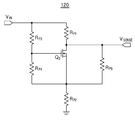
다음으로, 도 4는 도 2의 LED 구동 장치에 채용될 수 있는 보호 회로의 일 실시 형태를 대략적으로 나타낸 회로도이다.Next, Fig. 4 is a circuit diagram schematically showing one embodiment of a protection circuit that can be employed in the LED driving apparatus of Fig.
도 4를 참조하면, 보호 회로(120)는 스위치 소자 Q3, 및 복수 개의 저항 RP1~RP5을 포함할 수 있다. 스위치 소자 Q3는 입력 전압 VIN에 의해 동작할 수 있으며, 보호 회로(120)가 출력하는 센싱 전압 VSENSE는 스위치 소자 Q3의 드레인 단자에서 측정되는 전압일 수 있다.Referring to FIG. 4, the
스위치 소자 Q3는 게이트-소스 전압 VGS가 스위치 소자 Q3의 문턱 전압보다 클 때 동작을 시작할 수 있다. 스위치 소자 Q3의 게이트 단자와 소스 단자 사이에 연결된 저항 RP4에 인가되는 전압 VGS는 아래의 수학식 1과 같이 표현될 수 있다. 스위치 소자 Q3의 문턱 전압보다 게이트-소스 전압 VGS가 커지는 데에 필요한 입력 전압 VIN의 값을 소정의 기준 전압으로 정의할 수 있다. 상기 기준 전압은, 구동 회로(110)가 발광부(13)의 동작에 필요한 전류 ILED를 공급하기 위한 최소한의 전압일 수 있다.Switch element Q 3 can start operating when the gate-source voltage V GS is greater than the threshold voltage of switch element Q 3 . The voltage V GS applied to the resistor R P4 connected between the gate terminal and the source terminal of the switch element Q 3 can be expressed by Equation 1 below. The value of the input voltage V IN required for the gate-source voltage V GS to be larger than the threshold voltage of the switching element Q 3 can be defined as a predetermined reference voltage. The reference voltage may be a minimum voltage for supplying the current I LED required for the operation of the

수학식 1에서 저항은 모두 고정된 값이므로, 입력 전압 VIN이 증가하여 상기 기준 전압보다 커지는 경우 스위치 소자 Q3이 턴-온될 수 있다. 입력 전압 VIN이 상기 기준 전압보다 작아서 스위치 소자 Q3가 턴-오프되어 있는 동안, 보호 회로(120)의 출력 전압 VSENSE는 아래의 수학식 2와 같이 표현될 수 있다.Since the resistances in Equation (1) are all fixed values, when the input voltage V IN increases and becomes larger than the reference voltage, the switch element Q 3 can be turned on. The output voltage V SENSE of the
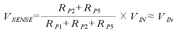
한편, 도 4에 도시한 보호 회로(120)에서, 스위치 소자 Q3의 드레인 단자와 소스 단자 사이에 연결되는 저항 RP5는 저항 RP1 및 RP2에 비해 매우 큰 값을 가질 수 있다. 따라서, 스위치 소자 Q3가 턴-오프 상태일 때, 보호 회로(120)의 출력 전압 VSENSE는 실질적으로 입력 전압 VIN과 거의 동일한 값을 가질 수 있다. VIN이 상기 기준 전압보다 커지면 스위치 소자 Q3가 턴-온되고, 센싱 전압 VSENSE는 수학식 3과 같이 표현될 수 있다.On the other hand, in the

수학식 2와 수학식 3을 비교하면, 스위치 소자 Q3가 턴-온됨에 따라 저항 RP1 및 RP2에 비해 상대적으로 매우 큰 값을 갖는 저항 RP5가 센싱 전압 VSENSE을 결정하는 데에 영향을 끼치지 못 하게 되며, 센싱 전압 VSENSE는 감소할 수 있다. 즉, VIN이 증가하여 스위치 소자 Q3가 턴-온 상태에 진입하면, 보호 회로(120)의 출력 전압 VSENSE는 감소할 수 있다.Comparing the equations (2) and (3), it can be understood that a resistor R P5 having a relatively large value as compared with the resistances R P1 and R P2 as the switch element Q 3 is turned on affects the determination of the sensing voltage V SENSE And the sensing voltage V SENSE can be reduced. That is, when V IN increases and the switch element Q3 enters the turn-on state, the output voltage V SENSE of the
구동 회로(110)에 입력되는 입력 전압 VIN 대신 센싱 전압 VSENSE를 입력 전압으로 인식하여 동작하는 제어 회로(130)는, VSENSE의 값이 소정의 임계 전압보다 작을 때 구동 회로(110)가 전류 ILED를 광원부(13)에 공급하도록 설정될 수 있다. VIN이 증가하여 상기 기준 전압보다 커지면 스위치 소자 Q3가 턴-온되고, 보호 회로(120)의 출력 전압 VSENSE가 감소함에 따라 제어 회로(130)는 구동 회로(110)가 발광부(13)에 전류 ILED를 공급하도록 제어할 수 있다. 이하, 도 6을 함께 참조하여 설명한다.
The
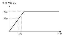
도 6은 도 4에 도시한 보호 회로의 동작을 설명하기 위한 그래프이다.6 is a graph for explaining the operation of the protection circuit shown in FIG.
도 6을 참조하면, 입력 전압 VIN은 직류 특성을 갖는 전압일 수 있다. 직류 특성을 갖는 입력 전압 VIN은 소정의 상승 시간(rising time) 동안 점점 증가하여 일정한 직류 전압 VDC을 공급할 수 있다. 직류 전압 VDC는, 기준 전압 VREF보다 클 수 있다. 기준 전압 VREF은 앞서 설명한 바와 같이 구동 회로(110)가 전류 ILED를 광원부(13)에 공급하는 데에 필요한 최소 전압일 수 있다.Referring to FIG. 6, the input voltage V IN may be a voltage having a direct current characteristic. The input voltage V IN having the direct current characteristic may gradually increase for a predetermined rising time to supply a constant direct current voltage V DC . The DC voltage V DC may be greater than the reference voltage V REF . The reference voltage V REF may be the minimum voltage necessary for the driving
입력 전압 VIN이 증가하여 기준 전압 VREF보다 커지면, 보호 회로(120)의 스위치 소자 Q3가 턴-온되며, 센싱 전압 VSENSE가 감소할 수 있다. 스위치 소자 Q3의 드레인 단자와 소스 단자 사이에 연결된 저항 RP5에 의해 스위치 소자 Q3가 턴-온된 이후 센싱 전압 VSENSE이 수학식 3에 의해 표현되는 값을 가질 때까지 소정의 지연 시간이 필요할 수 있다. 따라서, 도 6에 도시한 시점 t1이 아닌, 시점 t2에서 센싱 전압 VSENSE가 수학식 3에 의해 표현되는 값을 가질 수 있으며, 제어 회로(130)가 구동 회로(110)를 동작시켜 전류 ILED를 광원부(13)에 공급할 수 있다.When the input voltage V IN increases and becomes larger than the reference voltage V REF , the switch element Q 3 of the
즉, 스위치 소자 Q3의 히스테리시스(hysteresis) 특성으로 인해, 스위치 소자 Q3가 턴-온되고 제어 회로(130)가 동작할 수 있는 값까지 센싱 전압 VSENSE가 감소하는 데에 일정한 시간(t2-t1)이 필요할 수 있다. 따라서, 입력 전압 VIN이 상기 기준 전압 부근의 값에서 증감을 반복하는 구간에서 발생할 수 있는 발광부(13)의 채터링(chattering) 현상을 방지하고 구동 회로(110) 및 제어 회로(130) 등에 가해지는 스트레스를 줄일 수 있다.That is, due to the hysteresis (hysteresis) properties of the switching element Q 3, a switching element Q 3 is turned on and a certain time to the sensed voltage V SENSE reduced to a value that can be controlled by the
구동 회로(110)가 도 3에 도시한 실시 형태와 같이 부스트 컨버터 회로를 포함하는 경우, 입력 전압 VIN이 감소하면 구동 회로(110)의 출력을 유지하기 위해 구동 회로(110)에 입력되는 전류가 증가할 수 있다. 따라서, 입력 전압 VIN이 감소할 때 구동 회로(110)에 포함되는 회로 소자에 가해지는 스트레스를 줄이기 위해 구동 회로(110)에 입력되는 전류 증가를 억제할 필요가 있다. When the driving
본 발명의 실시 형태에서는, VIN이 감소할 때 센싱 전압 VSENSE가 VIN의 감소량보다 빠르게 증가하며, 제어 회로(130)는 구동 회로(110)가 출력하는 전류 ILED가 빠르게 감소하도록 구동 회로(110)의 동작을 제어한다. 즉, 입력 전압 VIN의 감소량보다 구동 회로(110)가 출력하는 ILED의 감소량이 크기 때문에, 출력을 유지하기 위해 구동 회로(110)에 과전류가 인가되지 않음으로써 구동 회로(110)에 가해지는 스트레스를 줄일 수 있다.
In the embodiment of the present invention, when V IN decreases, the sensing voltage V SENSE increases faster than the decrease amount of V IN , and the
도 5는 본 발명의 일 실시 형태에 따른 LED 구동 장치를 나타낸 회로도이다.5 is a circuit diagram showing an LED driving apparatus according to an embodiment of the present invention.
도 5를 참조하면, 본 발명의 실시 형태에 따른 LED 구동 장치(100)는 구동 회로(110), 보호 회로(120) 및 제어 회로(130)를 포함할 수 있다. 구동 회로(110)는 앞서 설명한 바와 같이 발광부(13)에 포함되는 LED에 전류 ILED를 공급하는 DC-DC 컨버터를 포함할 수 있다. 도 5를 참조하면, 구동 회로(110)는 부스트 컨버터(113)와 전류 검출 회로(115)를 포함할 수 있다. Referring to FIG. 5, the
부스트 컨버터(113)는 스위치 소자 Q1을 포함하며, 제어 회로(130)는 스위치 소자 Q1의 온/오프를 조절하여 부스트 컨버터(113)가 출력하는 전류 ILED의 크기를 제어할 수 있다. 구동 회로(110)와 연결된 전원부(11)가 전압 VBT를 출력하는 경우, 전압 VBT는 다이오드 D1을 거쳐 부스트 컨버터(113)의 입력단에 입력 전압 VIN으로 공급될 수 있다. 입력 전압 VIN에 포함된 노이즈 성분은 커패시터 C1을 통해 제거될 수 있으며, 스위치 소자 Q1이 턴-온 되어 있는 동안 입력 전압 VIN에 의해 인덕터 L에 에너지가 저장될 수 있다. 인덕터 L에 저장된 에너지는 스위치 소자 Q1이 턴-오프되는 동안 제너 다이오드 D2를 거쳐서 광원부(13)에 전류 ILED로 공급될 수 있다. 즉, 부스트 컨버터(113)가 출력하는 전류 ILED는 스위치 소자 Q1의 동작에 의해 결정될 수 있으며, 제어 회로(130)는 PWM 디밍 또는 아날로그 디밍 등에 의해 제어 핀 CTRL을 통해 출력되는 신호의 듀티 비 등을 조절하여 스위치 소자 Q1의 온/오프 타이밍을 조절할 수 있다.The
전류 검출 회로(115)는 스위치 소자 Q2와, 전류 검출을 위한 저항 R2를 포함할 수 있다. 제어 회로(130)의 전류 검출 핀 VOUT은 저항 R2와 연결되어 전류 ILED를 전압 형식으로 검출할 수 있으며, 스위치 소자 Q2는 제어 회로(130)의 구동 핀 DIM과 연결될 수 있다. 제어 회로(130)가 핀 DIM을 통해 로우(LOW) 신호를 출력하는 경우, 스위치 소자 Q2가 턴-오프되어 광원부(13)에 공급되는 전류 ILED가 차단될 수 있다. 즉, 스위치 소자 Q2는 제어 회로(130)가 광원부(13)의 동작 여부를 조절하는 데에 이용될 수 있다.The
제어 회로(130)는 전류 검출 핀 VOUT을 통해 검출하는 전류 ILED와, 입력 핀 IN을 통해 전달되는 입력 전압을 이용하여 구동 회로(110)의 동작을 제어할 수 있다. 제어 회로(130)의 입력 핀 IN에는 보호 회로(120)가 출력하는 센싱 전압 VSENSE가 공급될 수 있으며, 제어 회로(130)는 센싱 전압 VSENSE가 소정의 임계 전압보다 작은 값을 가질 때 구동 회로(110)의 동작을 개시하도록 설정될 수 있다. The
직류 특성을 갖는 입력 전압 VIN이 공급되기 시작하면 일정한 직류 전압까지 상승하기 위한 상승 시간(rising time)이 필요하며, 입력 전압 VIN이 차단되면 접지 전압(0V)까지 VIN이 감소하기 위한 하강 시간(falling time)이 필요할 수 있다. 상승 시간 및 하강 시간에 대한 고려 없이 구동 회로(110)의 동작을 제어하는 경우, 입력 전압 VIN이 구동 회로(110)의 동작에 필요한 최소한의 기준 전압과 유사한 값을 가질 때, 구동 회로(110)의 동작이 불안정할 수 있다. 본 발명의 실시 형태에서는 보호 회로(120)를 적용함으로써 상기와 같은 문제를 해결할 수 있다. 이하, 도 6을 함께 참조하여 보호 회로(120)의 동작을 설명한다.
When the input voltage V IN with the direct current characteristic starts to be supplied requires a rise time (rising time) to rise to a certain direct current voltage, the input voltage V IN is when lowered to V IN is reduced to the ground voltage (0V) block A falling time may be required. When the operation of the driving
전원부(13)로부터 전압 VBT가 공급되기 시작하면, 입력 전압 VIN이 소정의 상승 시간 동안 증가할 수 있다. 입력 전압 VIN이 기준 전압 VREF보다 작으면, 스위치 소자 Q3는 턴-오프 상태를 유지하고 제어 회로(130)의 입력 핀 IN에 전달되는 센싱 전압 VSENSE는 수학식 2와 같이 결정될 수 있다. 저항 RP5가 다른 저항 RP1, RP2에 비해 매우 큰 값을 가지므로, 스위치 소자 Q3가 턴-오프되어 있는 동안 센싱 전압 VSENSE는 입력 전압 VIN과 거의 동일한 값을 가질 수 있다.When the voltage V BT starts to be supplied from the
입력 전압 VIN이 증가하여 기준 전압 VREF보다 커지면 스위치 소자 Q3가 턴-온되고, 센싱 전압 VSENSE는 수학식 3과 같이 결정되어 스위치 소자 Q3가 턴-온되기 직전에 비해 감소할 수 있다. 다만, 센싱 전압 VSENSE는 스위치 소자 Q3의 드레인 단자와 소스 단자 사이에 연결된 저항 RP5에 의해 서서히 감소할 수 있다. 결국, 도 6에 도시한 바와 같이, 입력 전압 VIN이 기준 전압 VREF보다 커지는 시점 t1이 아닌, 어느 정도 시간이 경과한 이후인 t2에서 센싱 전압 VSENSE가 수학식 3에 의해 결정되는 값을 가질 수 있다. When the input voltage V IN increases and becomes larger than the reference voltage V REF , the switching element Q 3 is turned on, and the sensing voltage V SENSE is determined as shown in Equation 3, so that the switching element Q 3 can be reduced have. However, the sensing voltage V SENSE can be gradually reduced by the resistor R P5 connected between the drain terminal and the source terminal of the switch element Q3. As a result, as shown in Fig. 6, the sensing voltage V SENSE is determined by the equation (3) at t 2 after a certain time elapses, not at the time t 1 when the input voltage V IN becomes larger than the reference voltage V REF Value. ≪ / RTI >
따라서, 제어 회로(130)는 시점 t2 이후부터 구동 회로(110)를 동작시킬 수 있다. 예를 들어, 제어 회로(130)는 시점 t2 이후 스위치 소자 Q2를 턴-온 시켜 광원부(130)에 전류 ILED가 공급되도록 제어할 수 있으며, 제어 핀 CTRL을 통해 스위치 소자 Q1에 소정의 듀티 비를 갖는 PWM 신호를 공급하여 전류 ILED의 크기를 조절할 수 있다.Therefore, the
도 6의 그래프에서, 기준 전압 VREF는 구동 회로(110)가 광원부(13)를 구동할 수 있는 전류 ILED를 출력하는 데에 필요한 최소한의 전압일 수 있다. 본 발명에서는, 보호 회로(120)의 히스테리시스 특성을 이용하여 구동 회로(110)가 전류 ILED를 출력하는 타이밍을 소정 시간만큼 지연시킴으로써, 입력 전압 VIN이 기준 전압 VREF 부근의 값을 가질 때 발생할 수 있는 채터링(chattering) 문제를 해결할 수 있다.6, the reference voltage V REF may be a minimum voltage necessary for the driving
전원부(13)로부터 전압 VBT가 차단되면, 입력 전압 VIN이 감소할 수 있다. 입력 전압 VIN이 감소하여 기준 전압 VREF보다 작아지면, 보호 회로(120)가 출력하는 센싱 전압 VSENSE가 갑자기 증가할 수 있다. 따라서, 제어 회로(130)의 입력 핀 IN에 높은 레벨의 전압이 전달되어 제어 회로(130)는 스위치 소자 Q2를 턴-오프시키고 구동 회로(110)의 동작을 중지할 수 있다. 따라서, 입력 전압 VIN이 감소하여 기준 전압 VREF보다 작아졌을 때, 빠르게 구동 회로(110)의 동작을 중지시켜 회로에 가해지는 스트레스를 줄일 수 있다.
When the voltage V BT is cut off from the
한편, 도 3 내지 도 5를 참조하여 설명한 LED 구동 장치(100)는 아날로그 디밍 동작에도 효율적으로 적용될 수 있다. 아날로그 디밍을 이용하여 전류 ILED의 크기를 제어하는 경우, 입력 전압 VIN이 감소하면 따라 ILED가 함께 감소할 수 있다. 본원 발명의 실시 형태에서는 입력 전압 VIN이 감소하여 저전압 대역에 진입하였을 때, 전류 ILED를 빠르게 감소시켜 구동 회로(110)에 가해지는 스트레스를 최소화할 수 있다. 이하, 도 7을 참조하여 설명한다.Meanwhile, the
도 7은 도 5에 도시한 LED 구동 장치의 동작을 설명하기 위한 그래프이다. 도 7을 참조하면, 비교예로 도시한 그래프 A는 입력 전압 VIN가 단순히 전압 분배기(voltage divider)를 통해 제어 회로(130)의 입력 핀 IN에 공급되는 경우를 나타낼 수 있다. 본 발명의 실시 형태에 대응하는 그래프 B는 보호 회로(120)가 출력하는 센싱 전압 VSENSE가 제어 회로(130)의 입력 핀 IN에 공급되는 경우를 나타낼 수 있다. 입력 전압 VIN이 감소하여 저전압 대역에 진입하면, 스위치 소자 Q3는 턴-온 상태를 유지하며 선형 모드(linear region)에서 동작할 수 있다.7 is a graph for explaining the operation of the LED driving apparatus shown in FIG. Referring to FIG. 7, a graph A shown as a comparative example may show a case where the input voltage V IN is simply supplied to the input pin IN of the
도 7에 도시한 바와 같이 입력 전압 VIN이 감소하면, 스위치 소자 Q3의 게이트 - 소스 간 전압 VGS가 감소할 수 있다. 스위치 소자 Q3의 게이트 - 소스 간 전압 VGS가 감소함에 따라, 스위치 소자 Q3의 선형 모드 특성에 의해 드레인 전류 ID 및 드레인 - 소스 간 전압 VDS가 큰 폭으로 감소할 수 있다. 스위치 소자 Q3가 선형 모드에서 동작할 때 센싱 전압 VSENSE는 아래의 수학식 4와 같이 계산될 수 있다As shown in Fig. 7, when the input voltage V IN decreases, the gate-source voltage V GS of the switching element Q 3 can be reduced. As the source voltage V GS is reduced, the switching element Q 3 drain current by the linear-mode characteristics I D and the drain-gate of the switching element Q 3 is between the source voltage V DS can be reduced considerably. When the switching element Q 3 is operating in the linear mode, the sensing voltage V SENSE, may be computed as shown in Equation 4 below:
![]()
![]()
스위치 소자 Q3의 선형 모드 특성에 의해 드레인 전류 ID 및 드레인 - 소스 간 전압 VDS가 큰 폭으로 감소하므로, VSENSE 역시 큰 폭으로 감소할 수 있다. 아날로그 디밍 동작 시에 제어 회로(130)는 입력 핀 IN을 통해 공급되는 전압이 감소하는 경우, 구동 회로(110)에 입력되는 전압이 감소한 것으로 판단하여 전류 ILED의 크기를 감소시킬 수 있다. 따라서, 본 발명의 실시 형태에 따른 보호 회로(120)가 적용된 LED 구동 장치(100)에 아날로그 디밍을 적용하는 경우, 입력 전압 VIN이 저전압 대역에서 감소할 때 전류 ILED를 빠르게 감소시켜 구동 회로(110)에 포함되는 회로 소자에 작용하는 스트레스를 줄이고 회로의 신뢰성을 높일 수 있다.
The drain current I D and the drain-source voltage V DS are greatly reduced due to the linear mode characteristic of the switching device Q 3 , so that V SENSE can also be greatly reduced. In the analog dimming operation, when the voltage supplied through the input pin IN decreases, the
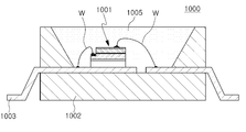
도 8 및 도 9는 본 발명의 일 실시 형태에 따른 조명 장치에 적용될 수 있는 LED 패키지를 나타낸 것이다.8 and 9 show an LED package that can be applied to a lighting device according to an embodiment of the present invention.
도 8을 참조하면, 반도체 발광소자 패키지(1000)는 반도체 발광소자(1001), 패키지 본체(1002) 및 한 쌍의 리드 프레임(1003)을 포함하며, 반도체 발광소자(1001)는 리드 프레임(1003)에 실장되어 와이어(W)를 통하여 리드 프레임(1003)과 전기적으로 연결될 수 있다. 실시 형태에 따라, 반도체 발광소자(1001)는 리드 프레임(1003) 아닌 다른 영역, 예컨대, 패키지 본체(1002)에 실장될 수도 있을 것이다. 또한, 패키지 본체(1002)는 빛의 반사 효율이 향상되도록 컵 형상을 가질 수 있으며, 이러한 반사컵에는 반도체 발광소자(1001)와 와이어(W) 등을 봉지하도록 투광성 물질로 이루어진 봉지체(1005)가 형성될 수 있다.
8, the semiconductor light emitting
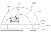
도 9를 참조하면, 반도체 발광소자 패키지(2000)는 반도체 발광소자(2001), 실장 기판(2010) 및 봉지체(2003)를 포함한다. 또한, 반도체 발광소자(2001)의 표면 및 측면에는 파장변환부(2002)가 형성될 수 있다. 반도체 발광소자(2001)는 실장 기판(2010)에 실장되어 와이어(W) 및 도전성 기판(2009)을 통하여 실장 기판(2010)과 전기적으로 연결될 수 있다. Referring to FIG. 9, a semiconductor light emitting
실장 기판(2010)은 기판 본체(2011), 상면 전극(2013) 및 하면 전극(2014)을 구비할 수 있다. 또한, 실장 기판(2010)은 상면 전극(2013)과 하면 전극(2014)을 연결하는 관통 전극(2012)을 포함할 수 있다. 실장 기판(2010)은 PCB, MCPCB, MPCB, FPCB 등의 기판으로 제공될 수 있으며, 실장 기판(2010)의 구조는 다양한 형태로 응용될 수 있다. The mounting
파장변환부(2002)는 형광체나 양자점 등을 포함할 수 있다. 봉지체(2003)는 상면이 볼록한 돔 형상의 렌즈 구조로 형성될 수 있지만, 실시 형태에 따라, 표면을 볼록 또는 오목한 형상의 렌즈 구조로 형성함으로써 봉지체(2003) 상면을 통해 방출되는 빛의 지향각을 조절하는 것이 가능하다.
The
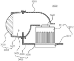
도 10은 본 발명의 일 실시 형태에 따른 조명 장치를 나타낸 도이다. 도 10을 참조하면, 본 발명의 일 실시 형태에 따른 조명 장치는 자동차용 헤드 램프에 적용될 수 있다.10 is a diagram showing a lighting apparatus according to an embodiment of the present invention. Referring to Fig. 10, the lighting device according to an embodiment of the present invention can be applied to a headlamp for an automobile.
도 10을 참조하면, 차량용 라이트 등으로 이용되는 헤드 램프(3000)는 광원(3001), 반사부(3005), 렌즈 커버부(3004)를 포함하며, 렌즈 커버부(3004)는 중공형의 가이드(3003) 및 렌즈(3002)를 포함할 수 있다. 또한, 헤드 램드(3000)는 광원(3001)에서 발생된 열을 외부로 방출하는 방열부(3012)를 더 포함할 수 있으며, 방열부(3012)는 효과적인 방열이 수행되도록 히트싱크(3010)와 냉각팬(3011)을 포함할 수 있다. 또한, 헤드 램프(3000)는 방열부(3012) 및 반사부(3005)를 고정시켜 지지하는 하우징(3009)을 더 포함할 수 있으며, 하우징(3009)은 일면에 방열부(3012)가 결합하여 장착되기 위한 중앙홀(3008)을 구비할 수 있다. 또한, 하우징(3009)은 상기 일면과 일체로 연결되어 직각방향으로 절곡되는 타면에 반사부(3005)가 광원(3001)의 상부측에 위치하도록 고정시키는 전방홀(3007)을 구비할 수 있다. 이에 따라, 반사부(3005)에 의하여 전방측은 개방되며, 개방된 전방이 전방홀(3007)과 대응되도록 반사부(3005)가 하우징(3009)에 고정되어 반사부(3005)를 통해 반사된 빛이 전방홀(3007)을 통과하여 외부로 출사될 수 있다.
10, a
본 발명은 상술한 실시형태 및 첨부된 도면에 의해 한정되는 것이 아니며 첨부된 청구범위에 의해 한정하고자 한다. 따라서, 청구범위에 기재된 본 발명의 기술적 사상을 벗어나지 않는 범위 내에서 당 기술분야의 통상의 지식을 가진 자에 의해 다양한 형태의 치환, 변형 및 변경이 가능할 것이며, 이 또한 본 발명의 범위에 속한다고 할 것이다.
The present invention is not limited to the above-described embodiment and the accompanying drawings, but is intended to be limited by the appended claims. It will be apparent to those skilled in the art that various changes in form and details may be made therein without departing from the spirit and scope of the invention as defined by the appended claims. something to do.
10 : 조명 장치
11 : 전원부
12 : LED 구동부
13 : 광원부
110 : 구동 회로
120 : 보호 회로
130 : 제어 회로10: Lighting device
11:
12: LED driver
13: Light source
110: drive circuit
120: Protection circuit
130: control circuit
Claims (10)
상기 입력 전압을 검출하여 센싱 전압을 출력하며, 상기 입력 전압이 증가하여 소정의 기준 전압보다 커지거나 상기 입력 전압이 감소하여 상기 기준 전압보다 작아질 때 히스테리시스 특성을 갖고 동작하는 회로 소자를 포함하는 보호 회로; 및
상기 센싱 전압 및 상기 구동 전류를 검출하여 상기 구동 회로의 동작을 제어하는 제어 회로; 를 포함하는 LED 구동 장치.
A driving circuit for outputting a driving current for driving a plurality of LEDs using an input voltage;
And a circuit element which operates with a hysteresis characteristic when the input voltage increases and becomes greater than a predetermined reference voltage or when the input voltage decreases and becomes smaller than the reference voltage by detecting the input voltage and outputting a sensing voltage. Circuit; And
A control circuit for detecting the sensing voltage and the driving current and controlling the operation of the driving circuit; And the LED driving device.
상기 보호 회로는, 상기 입력 전압이 증가하여 소정의 기준 전압보다 커지면, 상기 회로 소자를 턴-온시켜 상기 센싱 전압을 감소시키는 LED 구동 장치.
The method according to claim 1,
Wherein the protection circuit reduces the sensing voltage by turning on the circuit element when the input voltage increases and becomes greater than a predetermined reference voltage.
상기 제어 회로는, 상기 센싱 전압이 소정의 임계 전압보다 작아지면, 상기 구동 회로가 상기 구동 전류를 출력하도록 제어하는 LED 구동 장치.
3. The method of claim 2,
Wherein the control circuit controls the drive circuit to output the drive current when the sensing voltage becomes smaller than a predetermined threshold voltage.
상기 구동 회로는 상기 복수의 LED를 구동하기 위한 정전류를 생성하는 부스트 컨버터와 벅 컨버터 중 적어도 하나를 포함하며,
상기 제어 회로는 상기 부스트 컨버터와 상기 벅 컨버터 중 적어도 하나에 포함되는 스위치 소자의 동작을 제어하는 LED 구동 장치.
The method according to claim 1,
Wherein the driving circuit includes at least one of a boost converter and a buck converter for generating a constant current for driving the plurality of LEDs,
Wherein the control circuit controls operation of a switch element included in at least one of the boost converter and the buck converter.
상기 제어 회로는 상기 센싱 전압을 아날로그 디밍 신호로 이용하여 상기 스위치 소자의 동작을 제어하는 LED 구동 장치.
5. The method of claim 4,
Wherein the control circuit controls the operation of the switch element using the sensing voltage as an analog dimming signal.
상기 보호 회로는, 상기 입력 전압이 감소하면, 상기 센싱 전압을 상기 입력 전압의 감소량보다 크게 감소시키는 LED 구동 장치.
The method according to claim 1,
Wherein the protection circuit reduces the sensing voltage to a value greater than a reduction amount of the input voltage when the input voltage decreases.
상기 제어 회로는, 상기 입력 전압이 감소하면, 상기 센싱 전압의 감소량을 반영하여 상기 구동 전류가 감소하도록 상기 구동 회로를 제어하는 LED 구동 장치.
The method according to claim 6,
Wherein the control circuit controls the driving circuit so that the driving current is reduced by reflecting a decrease amount of the sensing voltage when the input voltage decreases.
상기 보호 회로는, 상기 회로 소자로 제공되는 전계 효과 트랜지스터(FET), 상기 입력 전압을 분배하여 상기 전계 효과 트랜지스터(FET)에 전달하는 전압 분배 저항, 및 상기 전계 효과 트랜지스터의 드레인 단자와 소스 단자 사이에 연결되어 히스테리시스 특성을 구현하는 히스테리시스 저항을 포함하는 LED 구동 장치.
The method according to claim 1,
The protection circuit includes a field effect transistor (FET) provided to the circuit element, a voltage distribution resistor for distributing the input voltage to the field effect transistor (FET), and a drain terminal And a hysteresis resistor connected to the resistor and implementing a hysteresis characteristic.
직류 입력 전압을 검출하여 센싱 전압을 생성하는 보호 회로와, 상기 센싱 전압에 기초하여 상기 복수의 LED를 동작하는 구동 전류를 출력하는 구동 회로를 갖는 LED 구동부; 를 포함하며,
상기 보호 회로는 상기 직류 입력 전압이 차단되면, 상기 직류 입력 전압의 감소량보다 상기 센싱 전압을 크게 감소시키며,
상기 LED 구동부는 상기 센싱 전압의 감소량에 기초하여 상기 구동 전류를 감소시키는 조명 장치.
A light source unit including a plurality of LEDs; And
An LED driver having a protection circuit for detecting a DC input voltage to generate a sensing voltage and a driving circuit for outputting a driving current for operating the plurality of LEDs based on the sensing voltage; / RTI >
Wherein the protection circuit significantly reduces the sensing voltage when the DC input voltage is cut off,
Wherein the LED driver reduces the driving current based on a reduction amount of the sensing voltage.
상기 보호 회로는, 상기 입력 전압이 증가하여 소정의 기준 전압보다 커지면, 소정의 지연 시간이 경과한 후에 상기 센싱 전압이 소정의 임계 전압보다 작아지도록 상기 센싱 전압을 감소시키는 조명 장치.
10. The method of claim 9,
Wherein the protection circuit decreases the sensing voltage so that the sensing voltage becomes smaller than a predetermined threshold voltage after a predetermined delay time elapses when the input voltage increases and becomes larger than a predetermined reference voltage.
Priority Applications (2)
| Application Number | Priority Date | Filing Date | Title |
|---|---|---|---|
| KR1020140101115A KR20160017841A (en) | 2014-08-06 | 2014-08-06 | Led driving device and lighting device |
| US14/636,600 US20160044757A1 (en) | 2014-08-06 | 2015-03-03 | Led driving device and lighting apparatus |
Applications Claiming Priority (1)
| Application Number | Priority Date | Filing Date | Title |
|---|---|---|---|
| KR1020140101115A KR20160017841A (en) | 2014-08-06 | 2014-08-06 | Led driving device and lighting device |
Publications (1)
| Publication Number | Publication Date |
|---|---|
| KR20160017841A true KR20160017841A (en) | 2016-02-17 |
Family
ID=55268528
Family Applications (1)
| Application Number | Title | Priority Date | Filing Date |
|---|---|---|---|
| KR1020140101115A Withdrawn KR20160017841A (en) | 2014-08-06 | 2014-08-06 | Led driving device and lighting device |
Country Status (2)
| Country | Link |
|---|---|
| US (1) | US20160044757A1 (en) |
| KR (1) | KR20160017841A (en) |
Cited By (4)
| Publication number | Priority date | Publication date | Assignee | Title |
|---|---|---|---|---|
| KR20170124032A (en) * | 2016-04-29 | 2017-11-09 | 엘지이노텍 주식회사 | Light emitting device and light emitting device for automobile using the same |
| WO2018128216A1 (en) * | 2017-01-09 | 2018-07-12 | 주식회사 실리콘마이터스 | Multi-channel switching converter |
| KR20180090552A (en) * | 2017-02-03 | 2018-08-13 | 엘지이노텍 주식회사 | Light emitting device and litht emitting device for automobile using the same |
| US10665152B2 (en) | 2016-09-06 | 2020-05-26 | Samsung Electronics Co., Ltd. | Light emitting diode display device and method of operating the same |
Families Citing this family (8)
| Publication number | Priority date | Publication date | Assignee | Title |
|---|---|---|---|---|
| JP2016213171A (en) | 2015-04-30 | 2016-12-15 | ソニー株式会社 | Light source control device, light source control method, and projector |
| JP2017021938A (en) * | 2015-07-08 | 2017-01-26 | パナソニックIpマネジメント株式会社 | Dimming control unit, lighting system, and equipment |
| CN106448577B (en) * | 2016-11-29 | 2019-02-26 | 深圳创维-Rgb电子有限公司 | A backlight constant current driver board and LCD TV |
| US10462860B2 (en) * | 2017-08-23 | 2019-10-29 | Elite Semiconductor Memory Technology Inc. | Controller for switching regulator, switching regulator and LED lighting system |
| CN110035582B (en) * | 2019-04-22 | 2024-08-23 | 晨辉光宝科技股份有限公司 | LED lamp tube |
| CN110012575B (en) * | 2019-05-09 | 2024-04-19 | 杭州必易微电子有限公司 | Drive control circuit and control method |
| FR3116409B1 (en) * | 2020-11-18 | 2022-12-16 | Valeo Vision | LIGHTING SYSTEM FOR MOTOR VEHICLES |
| US11849514B1 (en) * | 2022-06-10 | 2023-12-19 | Infineon Technologies Ag | Current regulator circuits with self-adaptive power offloading |
Family Cites Families (2)
| Publication number | Priority date | Publication date | Assignee | Title |
|---|---|---|---|---|
| US20120326618A1 (en) * | 2011-06-24 | 2012-12-27 | National Semiconductor Corporation | Harmonic ripple-current light emitting diode (led) driver circuitry and method |
| JP5754343B2 (en) * | 2011-10-25 | 2015-07-29 | ミツミ電機株式会社 | Low voltage detection circuit |
-
2014
- 2014-08-06 KR KR1020140101115A patent/KR20160017841A/en not_active Withdrawn
-
2015
- 2015-03-03 US US14/636,600 patent/US20160044757A1/en not_active Abandoned
Cited By (4)
| Publication number | Priority date | Publication date | Assignee | Title |
|---|---|---|---|---|
| KR20170124032A (en) * | 2016-04-29 | 2017-11-09 | 엘지이노텍 주식회사 | Light emitting device and light emitting device for automobile using the same |
| US10665152B2 (en) | 2016-09-06 | 2020-05-26 | Samsung Electronics Co., Ltd. | Light emitting diode display device and method of operating the same |
| WO2018128216A1 (en) * | 2017-01-09 | 2018-07-12 | 주식회사 실리콘마이터스 | Multi-channel switching converter |
| KR20180090552A (en) * | 2017-02-03 | 2018-08-13 | 엘지이노텍 주식회사 | Light emitting device and litht emitting device for automobile using the same |
Also Published As
| Publication number | Publication date |
|---|---|
| US20160044757A1 (en) | 2016-02-11 |
Similar Documents
| Publication | Publication Date | Title |
|---|---|---|
| KR20160017841A (en) | Led driving device and lighting device | |
| US9307593B1 (en) | Dynamic bleeder current control for LED dimmers | |
| US9603207B2 (en) | Driving circuit, illumination light source, and illumination device | |
| JP5435912B2 (en) | Power supply device and lighting device | |
| US10076010B2 (en) | Lighting device, and luminaire | |
| US7301784B2 (en) | Lighting control unit for vehicle lighting fixture | |
| CN104427720B (en) | Lighting device and illumination apparatus using the same | |
| JP2006108260A (en) | Light emitting diode driving semiconductor circuit and light emitting diode driving device having the same | |
| US9801247B2 (en) | Light-dimming device | |
| JP2008310963A (en) | LED lighting device and LED lighting apparatus | |
| US9210743B2 (en) | Lighting device, lighting fixture, lamp, and sound emission prevention method | |
| JP2010015887A (en) | Led lighting control circuit and vehicle lamp fixture equipped with this | |
| US9055638B2 (en) | Lighting device and lighting fixture | |
| KR20150145290A (en) | DRIVING DEVICE FOR LEDs AND LIGHTING DEVICE INCLUDING THEM | |
| JP2010056314A (en) | Driving circuit of light-emitting diode, light-emitting device using the same, and lighting device | |
| US8698416B2 (en) | Continuous dimming AC LED device | |
| KR102277126B1 (en) | DRIVING DEVICE FOR LEDs AND LIGHTING DEVICE | |
| US8922125B2 (en) | Occupancy sensor for controlling an LED light | |
| US9295138B2 (en) | Lighting device and luminaire using the same | |
| US9265107B2 (en) | LED driving device, lighting device and control circuit for LED driving device | |
| CN204986459U (en) | Light emitting diode lamp | |
| KR101326988B1 (en) | Bleed circuit, lighting control circuit and method thereof | |
| CN108174493A (en) | The control method of ignition device, luminaire and ignition device | |
| JP2016170985A (en) | Lighting circuit, luminaire and illumination system | |
| CN104427722B (en) | Lighting device and illumination apparatus using the same |
Legal Events
| Date | Code | Title | Description |
|---|---|---|---|
| PA0109 | Patent application |
Patent event code: PA01091R01D Comment text: Patent Application Patent event date: 20140806 |
|
| PG1501 | Laying open of application | ||
| PC1203 | Withdrawal of no request for examination | ||
| WITN | Application deemed withdrawn, e.g. because no request for examination was filed or no examination fee was paid |