KR20160016890A - Circuit and layout techniques for flop tray area and power optimization - Google Patents
Circuit and layout techniques for flop tray area and power optimization Download PDFInfo
- Publication number
- KR20160016890A KR20160016890A KR1020157036440A KR20157036440A KR20160016890A KR 20160016890 A KR20160016890 A KR 20160016890A KR 1020157036440 A KR1020157036440 A KR 1020157036440A KR 20157036440 A KR20157036440 A KR 20157036440A KR 20160016890 A KR20160016890 A KR 20160016890A
- Authority
- KR
- South Korea
- Prior art keywords
- flop
- scan
- flip
- input
- signal
- Prior art date
Links
Images

Classifications
-
- G—PHYSICS
- G01—MEASURING; TESTING
- G01R—MEASURING ELECTRIC VARIABLES; MEASURING MAGNETIC VARIABLES
- G01R31/00—Arrangements for testing electric properties; Arrangements for locating electric faults; Arrangements for electrical testing characterised by what is being tested not provided for elsewhere
- G01R31/28—Testing of electronic circuits, e.g. by signal tracer
- G01R31/317—Testing of digital circuits
- G01R31/3177—Testing of logic operation, e.g. by logic analysers
-
- G—PHYSICS
- G01—MEASURING; TESTING
- G01R—MEASURING ELECTRIC VARIABLES; MEASURING MAGNETIC VARIABLES
- G01R31/00—Arrangements for testing electric properties; Arrangements for locating electric faults; Arrangements for electrical testing characterised by what is being tested not provided for elsewhere
- G01R31/28—Testing of electronic circuits, e.g. by signal tracer
- G01R31/317—Testing of digital circuits
- G01R31/3181—Functional testing
- G01R31/3183—Generation of test inputs, e.g. test vectors, patterns or sequences
-
- G—PHYSICS
- G01—MEASURING; TESTING
- G01R—MEASURING ELECTRIC VARIABLES; MEASURING MAGNETIC VARIABLES
- G01R31/00—Arrangements for testing electric properties; Arrangements for locating electric faults; Arrangements for electrical testing characterised by what is being tested not provided for elsewhere
- G01R31/28—Testing of electronic circuits, e.g. by signal tracer
- G01R31/317—Testing of digital circuits
- G01R31/3181—Functional testing
- G01R31/3185—Reconfiguring for testing, e.g. LSSD, partitioning
- G01R31/318533—Reconfiguring for testing, e.g. LSSD, partitioning using scanning techniques, e.g. LSSD, Boundary Scan, JTAG
- G01R31/318541—Scan latches or cell details
Landscapes
- Engineering & Computer Science (AREA)
- General Engineering & Computer Science (AREA)
- Physics & Mathematics (AREA)
- General Physics & Mathematics (AREA)
- Tests Of Electronic Circuits (AREA)
- Test And Diagnosis Of Digital Computers (AREA)
- Semiconductor Integrated Circuits (AREA)
- Electronic Switches (AREA)
- Logic Circuits (AREA)
Abstract
스캔가능한 플롭 트레이에서 스캔 오버헤드를 감소시키기 위한 기술들이 본 명세서에 설명된다. 일 실시예에서, 플롭 트레이에 대한 스캔 회로는, 정상 모드에서, 입력 데이터 신호를 인버팅하여 인버팅된 데이터 신호를 플롭 트레이의 플립-플롭의 입력에 출력하고, 스캔 모드에서, 플립-플롭의 입력으로부터의 데이터 신호를 차단하도록 구성되는 3-상태 회로를 포함한다. 스캔 회로는 또한, 스캔 모드에서, 스캔 신호를 플립-플롭의 입력에 전달하고, 정상 모드에서, 플립-플롭의 입력으로부터의 스캔 신호를 차단하도록 구성되는 전달 게이트를 포함한다.Techniques for reducing scan overhead in a scanable flop tray are described herein. In one embodiment, the scan circuit for the flop tray, in normal mode, inverts the input data signal to output the inverted data signal to the input of the flip-flop of the flop tray, and in scan mode, the flip- And a three-state circuit configured to block the data signal from the input. The scan circuit also includes a transfer gate configured to transfer the scan signal to the input of the flip-flop in the scan mode and to block the scan signal from the input of the flip-flop in the normal mode.
Description
[0001] 본 개시의 양상들은 일반적으로 스캔가능한 플롭 트레이(flop tray)들에 관한 것으로, 더 상세하게는, 스캔가능한 플롭 트레이의 스캔 오버헤드(overhead)를 감소시키는 것에 관한 것이다.[0001] Aspects of the present disclosure relate generally to scanable flop trays, and more particularly to reducing the scan overhead of a scanable flop tray.
[0002] 플립-플롭(flip-flop)들은, 시스템의 다양한 컴포넌트들에 의한 프로세싱을 위한 하나 또는 그 초과의 데이터 신호들로부터 데이터 값들을 캡쳐(래칭(latch))하기 위해 시스템에서 사용될 수도 있다. 시스템은, 플립-플롭들이 테스팅 동안 정확하게 기능하고 있다는 것을 검증하기 위한 스캔 회로를 포함할 수도 있다. 이를 행하기 위해, 스캔 회로는, 알려진 테스트 패턴을 갖는 스캔 신호를 수신하고 플립-플롭들을 통해 스캔 신호를 스캔한다. 플립-플롭들을 통해 스캔 신호가 스캔된 후, 플립-플롭들이 정확하게 기능하고 있는지 여부를 결정하기 위해, 출력 스캔 신호는 기대되는 출력 스캔 신호와 비교된다. 기대되는 출력 스캔 신호는, 입력 스캔 신호의 알려진 테스트 패턴 및 플립-플롭들의 기대되는 기능에 기초할 수도 있다. 스캔 회로는, 스캔 회로에 의해 소모되는 전력 및 칩 영역으로 인해 시스템에 오버헤드를 부가한다.[0002] Flip-flops may be used in a system to capture (latch) data values from one or more data signals for processing by various components of the system. The system may include a scan circuit to verify that the flip-flops are functioning correctly during testing. To do this, the scan circuit receives a scan signal having a known test pattern and scans the scan signal through the flip-flops. After the scan signal is scanned through the flip-flops, the output scan signal is compared to the expected output scan signal to determine whether the flip-flops are functioning correctly. The expected output scan signal may be based on a known test pattern of the input scan signal and the expected function of the flip-flops. The scan circuit adds overhead to the system due to the power and chip area consumed by the scan circuit.
[0003] 다음은 하나 또는 그 초과의 실시예들의 기본적인 이해를 제공하기 위해 그러한 실시예들의 간략화된 개요를 제시한다. 이러한 개요는, 고려되는 모든 실시예들의 포괄적인 개관이 아니며, 모든 실시예들의 핵심 또는 중요 엘리먼트들을 식별하거나 임의의 실시예들 또는 모든 실시예들의 범위를 기술하도록 의도되지는 않는다. 그것의 유일한 목적은 이후에 제시되는 더 상세한 설명에 대한 서론으로서 간략화된 형태로 하나 또는 그 초과의 실시예들의 일부 개념들을 제시하는 것이다.[0003] The following presents a simplified summary of such embodiments in order to provide a basic understanding of one or more embodiments. This summary is not a comprehensive overview of all embodiments contemplated and is not intended to identify key or critical elements of all embodiments or to delineate the scope of any embodiments or all embodiments. Its sole purpose is to present some concepts of one or more embodiments in a simplified form as a prelude to the more detailed description that is presented later.
[0004] 일 양상에 따르면, 플롭 트레이에 대한 스캔 회로가 제공된다. 스캔 회로는, 정상 모드에서, 입력 데이터 신호를 인버팅(invert)하여 인버팅된 데이터 신호를 플롭 트레이의 플립-플롭의 입력에 출력하고, 스캔 모드에서, 플립-플롭의 입력으로부터의 데이터 신호를 차단(block)하도록 구성되는 3-상태(tri-state) 회로를 포함한다. 스캔 회로는 또한, 스캔 모드에서, 스캔 신호를 플립-플롭의 입력에 전달하고, 정상 모드에서, 플립-플롭의 입력으로부터의 스캔 신호를 차단하도록 구성되는 전달 게이트를 포함한다.[0004] According to one aspect, a scan circuit for a flop tray is provided. The scan circuit, in the normal mode, inverts the input data signal to output the inverted data signal to the input of the flip-flop of the flop tray, and in scan mode, the data signal from the input of the flip- State circuit that is configured to block the input signal. The scan circuit also includes a transfer gate configured to transfer the scan signal to the input of the flip-flop in the scan mode and to block the scan signal from the input of the flip-flop in the normal mode.
[0005] 제 2 양상은 플롭 트레이에 대한 스캔 회로에 관한 것이다. 스캔 회로는, 정상 모드에서 제 1 데이터 신호를 인버팅하여 인버팅된 제 1 데이터 신호를 플롭 트레이의 제 1 플립-플롭의 입력에 출력하고, 스캔 모드에서 제 1 플립-플롭의 입력으로부터의 제 1 데이터 신호를 차단하도록 구성되는 제 1 3-상태 회로를 포함한다. 스캔 회로는 또한, 스캔 모드에서, 스캔 신호를 제 1 플립-플롭의 입력에 전달하고, 정상 모드에서, 제 1 플립-플롭의 입력으로부터의 스캔 신호를 차단하도록 구성되는 제 1 전달 게이트를 포함한다. 스캔 회로는 또한, 정상 모드에서, 제 2 데이터 신호를 인버팅하여 인버팅된 제 2 데이터 신호를 플롭 트레이의 제 2 플립-플롭의 입력에 출력하고, 스캔 모드에서, 제 2 플립-플롭의 입력으로부터의 제 2 데이터 신호를 차단하도록 구성되는 제 2 3-상태 회로를 포함한다. 회로는 추가로, 스캔 모드에서 제 1 플립-플롭의 출력으로부터 제 2 플립-플롭의 입력으로 스캔 신호를 전달하고, 정상 모드에서 제 1 플립-플롭의 입력으로부터 제 2 플립-플롭의 출력으로의 스캔 신호를 차단하도록 구성되는 제 2 전달 게이트를 포함한다.[0005] A second aspect relates to a scan circuit for a flop tray. The scan circuit outputs the inverted first data signal to the input of the first flip-flop of the flop tray by inverting the first data signal in the normal mode, and outputs the first data signal from the first flip- Lt; RTI ID = 0.0 > 1-data < / RTI > The scan circuit also includes a first transfer gate configured to transfer the scan signal to the input of the first flip-flop in the scan mode and to block the scan signal from the input of the first flip-flop in the normal mode . The scan circuit also outputs the inverted second data signal to the input of the second flip-flop of the flop tray by inverting the second data signal in the normal mode, and in the scan mode, the input of the second flip- And a second 3-state circuit configured to cut off the second data signal from the second data line. The circuitry further comprises a scan driver for transferring the scan signal from the output of the first flip-flop to the input of the second flip-flop in scan mode and for transferring the scan signal from the input of the first flip- And a second transfer gate configured to block the scan signal.
[0006] 제 3 양상은 플롭 트레이를 스캔하기 위한 방법에 관한 것이다. 방법은, 정상 모드에서, 3-상태 회로를 사용하여, 입력 데이터 신호를 인버팅하고 인버팅된 데이터 신호를 플롭 트레이의 플립 플롭의 입력에 출력하는 단계, 및 스캔 모드에서, 3-상태 회로를 사용하여, 플립-플롭의 입력으로부터의 데이터 신호를 차단하는 단계를 포함한다. 방법은 또한, 스캔 모드에서, 전달 게이트를 사용하여 스캔 신호를 플립-플롭의 입력에 전달하는 단계, 및 정상 모드에서, 전달 게이트를 사용하여 플립-플롭의 입력으로부터의 스캔 신호를 차단하는 단계를 포함한다.[0006] A third aspect relates to a method for scanning a flop tray. The method includes the steps of inverting the input data signal and outputting the inverted data signal to the input of the flip flop of the flop tray in a normal mode using a three-state circuit, and in a scan mode, And blocking the data signal from the input of the flip-flop. The method also includes the steps of transferring the scan signal to the input of the flip-flop using the transfer gate in the scan mode and interrupting the scan signal from the input of the flip-flop using the transfer gate in the normal mode .
[0007] 제 4 양상은 플롭 트레이를 스캔하기 위한 장치에 관한 것이다. 장치는, 정상 모드에서, 입력 데이터 신호를 인버팅하고 인버팅된 데이터 신호를 플롭 트레이의 플립-플롭의 입력에 출력하기 위한 수단, 및 스캔 모드에서, 플립-플롭의 입력으로부터의 데이터 신호를 차단하기 위한 수단을 포함한다. 장치는 또한, 스캔 모드에서, 스캔 신호를 플립-플롭의 입력에 전달하기 위한 수단, 및 정상 모드에서, 플립-플롭의 입력으로부터의 스캔 신호를 차단하기 위한 수단을 포함한다.[0007] A fourth aspect relates to an apparatus for scanning a flop tray. The apparatus comprises means for inverting the input data signal and outputting the inverted data signal to the input of the flip-flop of the flop tray in a normal mode, and means for interrupting the data signal from the input of the flip- And < / RTI > The apparatus also includes means for delivering the scan signal to the input of the flip-flop in the scan mode, and means for interrupting the scan signal from the input of the flip-flop in the normal mode.
[0008] 상술한 목적 및 관련된 목적의 달성을 위해, 하나 또는 그 초과의 실시예들은 아래에서 완전히 설명되고 특히 청구항들에서 지적되는 특성들을 포함한다. 다음의 설명 및 첨부된 도면들은 하나 또는 그 초과의 실시예들의 특정한 예시적인 양상들을 상세하게 기재한다. 그러나, 이들 양상들은, 다양한 실시예들의 원리들이 이용될 수도 있는 다양한 방식들 중 단지 몇몇만을 표시하며, 설명된 실시예들은 모든 그러한 양상들 및 그들의 등가물들을 포함하도록 의도된다.[0008] To the accomplishment of the foregoing and related ends, one or more embodiments comprise the features hereinafter fully described and particularly pointed out in the claims. The following description and the annexed drawings set forth in detail certain illustrative aspects of one or more embodiments. However, these aspects are indicative only of a few of the various ways in which the principles of various embodiments may be employed, and the illustrated embodiments are intended to include all such aspects and their equivalents.
[0009] 도 1은 스캔가능한 플롭 트레이의 예를 도시한다.
[0010] 도 2는 멀티플렉서의 예를 도시한다.
[0011] 도 3은 본 개시의 일 실시예에 따른, 감소된 오버헤드를 갖는 스캔 멀티플렉서를 도시한다.
[0012] 도 4는 본 개시의 일 실시예에 따른, 일 플립-플롭의 출력과 다른 플립-플롭의 입력 사이에 커플링된 스캔 멀티플렉서를 도시한다.
[0013] 도 5는 본 개시의 실시예에 따른 스캔가능한 플롭 트레이를 도시한다.
[0014] 도 6은 본 개시의 특정한 실시예들에 따른, 감소된 스캔 오버헤드로 플롭 트레이를 스캔하기 위한 방법을 예시하는 흐름도이다.[0009] FIG. 1 shows an example of a scanable flop tray.
[0010] FIG. 2 shows an example of a multiplexer.
[0011] FIG. 3 illustrates a scan multiplexer with reduced overhead, according to one embodiment of the present disclosure.
[0012] FIG. 4 illustrates a scan multiplexer coupled between the output of one flip-flop and the input of another flip-flop, in accordance with one embodiment of the present disclosure.
[0013] FIG. 5 illustrates a scanable flop tray in accordance with an embodiment of the present disclosure.
[0014] FIG. 6 is a flow chart illustrating a method for scanning a flop tray with reduced scan overhead, in accordance with certain embodiments of the present disclosure.
[0015] 첨부된 도면들과 관련하여 아래에 기재되는 상세한 설명은, 다양한 구성들의 설명으로서 의도되며, 본 명세서에 설명된 개념들이 실시될 수 있는 유일한 구성들만을 표현하도록 의도되지 않는다. 상세한 설명은 다양한 개념들의 철저한 이해를 제공하려는 목적을 위해 특정한 세부사항들을 포함한다. 그러나, 이들 개념들이 이들 특정한 세부사항들 없이도 실시될 수도 있다는 것은 당업자들에게 명백할 것이다. 몇몇 예시들에서, 그러한 개념들을 불명료하게 하는 것을 회피하기 위해, 잘-알려진 구조들 및 컴포넌트들은 블록도 형태로 도시되어 있다.BRIEF DESCRIPTION OF THE DRAWINGS [0015] The following detailed description, taken in conjunction with the accompanying drawings, is intended as a description of various configurations and is not intended to represent the only configurations in which the concepts described herein may be practiced. The detailed description includes specific details for the purpose of providing a thorough understanding of the various concepts. However, it will be apparent to those skilled in the art that these concepts may be practiced without these specific details. In some instances, well-known structures and components are shown in block diagram form in order to avoid obscuring those concepts.
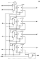
[0016] 도 1은 스캔가능한 플롭 트레이(100)의 예를 도시한다. 플롭 트레이(100)는 정상 모드 또는 스캔 모드에서 동작할 수 있다. 플롭 트레이(100)는, 플롭 트레이(100)의 정확한 기능을 테스트하기 위한 테스팅 동안 스캔 모드에서 동작된다.[0016] FIG. 1 shows an example of a
[0017] 플롭 트레이(100)는 제 1 D 플립-플롭(120a), 제 2 D 플립-플롭(120b), 제 3 D 플립-플롭(120c), 제 4 D 플립-플롭(120d), 및 스캔 회로(115)를 포함한다. 스캔 회로(115)는, 아래에서 추가로 설명되는 바와 같이, 테스팅 동안 플롭 트레이(100)를 스캔 모드에서 동작시키기 위해 사용된다. 스캔 회로(115)는 제 1 스캔 멀티플렉서(110a), 제 2 스캔 멀티플렉서(110b), 제 3 스캔 멀티플렉서(110c), 제 4 스캔 멀티플렉서(110d), 및 역-극성(inverted-polarity) NAND 게이트(130)를 포함한다. 각각의 스캔 멀티플렉서(110a-110d)는 D 플립-플롭들(120a-120d) 중 개별적인 하나에 커플링되며, 여기서, 제 1 스캔 멀티플렉서(110a)는 제 1 D 플립-플롭(120a)의 입력에 커플링되고, 제 2 스캔 멀티플렉서(110b)는 제 2 D 플립-플롭(120b)의 입력에 커플링되는 그러한 식이다. 스캔 회로(115)는 플롭 트레이(100)의 스캔 오버헤드를 구성한다.The
[0018] 정상 모드에서, 플롭 트레이(100)는 복수의 데이터 신호들 d0-d3을 병렬로 수신한다. 각각의 스캔 멀티플렉서(110a-110d)는 병렬 데이터 신호들 d0-d3 중 하나를 데이터 입력(도 1에서 "0"으로 라벨링됨)에서 수신하고, 개별적인 데이터 신호 d0-d3을 개별적인 D 플립-플롭(120a-120d)의 입력에 전달한다. 각각의 D 플립-플롭(120a-120d)은, 클록 신호 clk의 상승 또는 하강 엣지에서 개별적인 데이터 신호 d0-d3으로부터 데이터 값(예를 들어, 비트)을 캡쳐하고, 캡쳐된 데이터 값 q0-q3을 출력한다. 따라서, 각각의 클록 사이클 동안, 플롭 트레이(100)는, 클록 신호 clk의 상승 또는 하강 엣지에서 데이터 신호 d0-d3으로부터 병렬로 복수의 데이터 값들(예를 들어, 비트들)을 캡쳐하고, 캡쳐된 데이터 값들 q0-q3을 병렬로 출력한다. 도 1은 4개의 플립-플롭들을 포함하는 4-비트 플롭 트레이의 예를 도시한다. 그러나, 본 개시는 이러한 예로 제한되지 않으며, 임의의 개수의 플립-플롭들을 포함하는 플롭 트레이에 적용될 수 있음이 인식될 것이다.[0018] In the normal mode, the
[0019] 스캔 모드에서, 제 1 스캔 멀티플렉서(110a)는 플롭 트레이(100)의 스캔 입력(도 1에서 "sin"으로 라벨링됨)을 제 1 플립-플롭(120a)의 입력에 커플링시킨다. 나머지 스캔 멀티플렉서들(110b-110d) 각각은 앞선 D 플립-플롭의 nq 출력을 개별적인 D 플립-플롭의 입력에 커플링시킨다. 예를 들면, 제 2 스캔 멀티플렉서(110b)는 제 1 D 플립-플롭(120a)의 nq 출력을 제 2 D 플립-플롭(120b)의 입력에 커플링시키고, 제 3 멀티플렉서(110c)는 제 2 D 플립-플롭(120b)의 nq 출력을 제 3 D 플립-플롭(120c)의 입력에 커플링시키는 그러한 식이다. 각각의 멀티플렉서의 스캔 입력은 도 1에서 "1"로 라벨링된다. 제 4 D 플립-플롭(120d)(마지막 플립-플롭)의 nq 출력은 NAND 게이트(130)의 인버팅 입력에 커플링된다. 결과적으로, 스캔 신호가 스캔 입력("sin")에서 플롭 트레이(100)에 입력되는 경우, 스캔 신호는 플롭 트레이(100)의 D 플립-플롭들(120a-120d)을 통해 순차적으로 전파된다. 스캔 신호는 최종적으로, NAND 게이트(130)의 출력("sout"으로 라벨링됨)에서 출력된다. 출력 스캔 신호는, 플롭 트레이(100)의 스캔 입력("sin")으로부터 스캔 출력("sout")까지의 스캔 경로 내의 인버전(inversion)들의 개수에 의존하여, 입력 스캔 신호에 대해 인버팅될 수도 있거나 또는 넌-인버팅(non-invert)될 수도 있다.In scan mode, the
[0020] 따라서, 스캔 모드에서, 스캔 신호는 플롭 트레이(100)의 D 플립-플롭들(120a-120d)을 통해 스캔된다. 스캔 신호는 알려진 테스트 패턴을 포함할 수도 있고, 플롭 트레이(100)의 기능은, 알려진 테스트 패턴에 기초하여, 플롭 트레이(100)로부터의 출력 스캔 신호를 기대되는 출력 스캔 신호와 비교함으로써 평가될 수도 있다.[0020] Thus, in the scan mode, the scan signal is scanned through the D flip-
[0021] 도 1에 도시된 예에서, 플롭 트레이(100)의 동작 모드는 스캔 모드 입력(도 1에서 "scan"으로 라벨링됨)에서 수신되는 스캔 모드 신호에 의해 제어된다. 스캔 모드 신호는, 스캔 멀티플렉서가 개별적인 입력 데이터 신호 또는 스캔 신호를 개별적인 플립-플롭에 커플링시키는지 여부를 제어하기 위해 각각의 스캔 멀티플렉서(110a-110d)에 입력된다. 예를 들어, 스캔 모드 신호가 로직 0인 경우, 각각의 스캔 멀티플렉서(110a-110d)는 개별적인 입력 데이터 신호를 개별적인 플립-플롭에 커플링시킨다. 따라서, 스캔 모드 신호가 0인 경우 플롭 트레이는 정상 모드에서 동작한다. 스캔 모드 신호가 로직 1인 경우, 각각의 스캔 멀티플렉서(110a-110d)는 스캔 신호를 개별적인 플립-플롭에 커플링시킨다. 따라서, 스캔 모드 신호가 1인 경우 플롭 트레이는 스캔 모드에서 동작한다. 스캔 모드 신호는 또한, 도 1에 도시된 바와 같이, NAND 게이트(130)의 넌-인버팅 입력에 커플링될 수도 있다. 스캔 모드 신호가 0(정상 모드)인 경우, NAND 게이트(130)의 출력은 1로 고정된다.[0021] In the example shown in FIG. 1, the operating mode of the
[0022] 도 2는 제 1 스캔 멀티플렉서(110a) 및 제 1 D 플립-플롭(120a)의 예시적인 구현을 도시한다. 제 1 스캔 멀티플렉서(110a)는 제 1 3-상태 회로(215) 및 제 2 3-상태 회로(220)를 포함하며, 여기서, 각각의 3-상태 회로는 4개의 트랜지스터들(예를 들어, MOS(metal-oxide-semiconductor) 트랜지스터들)을 포함한다. 제 1 및 제 2 3-상태 회로들(215 및 220)은, 스캔 모드 입력(도 2에서 "scan"으로 라벨링됨)에서 수신되는 스캔 모드 신호에 의해 제어된다. 3-상태 회로들(215 및 220)은, 스캔 모드 신호가 0인 경우 정상 모드에서 동작하고 스캔 모드 신호가 1인 경우 스캔 모드에서 동작한다.[0022] FIG. 2 illustrates an exemplary implementation of a
[0023] 스캔 모드 신호가 0인 경우, 제 1 3-상태 회로(215)는 개별적인 입력 데이터 신호를 인버팅하고, 제 2 3-상태 회로(220)는 인버팅된 데이터 신호를 개별적인 D 플립-플롭(120a)의 입력에 전달한다. 도 2의 예에서, D 플립-플롭(120a)은 자신의 입력과 q 출력 사이에 홀수 개의 인버터들(즉, 인버터들(232, 234 및 236))을 갖는다. 홀수 개의 인버터들은 제 1 3-상태 회로(215)에 의한 로직 인버전을 원상태로 돌린다(undo). 결과적으로, 멀티플렉서(110a)의 데이터 입력으로부터 D 플립-플롭(120a)의 q 출력까지, 어떠한 로직 인버전도 존재하지 않는다.
[0024] 스캔 모드 신호가 1인 경우, 제 1 3-상태 회로(215)는 개별적인 데이터 입력을 차단한다. 제 2 3-상태 회로(220)는 개별적인 입력 스캔 신호를 인버팅하고, 인버팅된 스캔 신호를 개별적인 D 플립-플롭(120a)에 입력한다. 도 2의 예에서, D 플립-플롭(120a)은 자신의 입력과 nq 출력 사이에 짝수 개의 인버터들(즉, 인버터들(232 및 234))을 갖는다. 결과적으로, 멀티플렉서(110a)의 스캔 입력으로부터 D 플립-플롭(120a)의 nq 출력까지, 로직 인버전이 존재한다.When the scan mode signal is 1, the first 3-
[0025] 따라서, 정상 모드에서, 도 2의 스캔 멀티플렉서(110a)는 데이터 신호를 개별적인 플립-플롭(120a)에 출력하기 전에 입력 데이터 신호를 인버팅한다. 스캔 모드에서, 스캔 멀티플렉서(110a)는 스캔 신호를 개별적인 플립-플롭(120a)에 출력하기 전에 입력 스캔 신호를 인버팅한다. 따라서, 도 2의 스캔 멀티플렉서(110a)는 인버팅 멀티플렉서의 예이다.[0025] Thus, in the normal mode, the
[0026] 플롭 트레이(100) 내의 나머지 스캔 멀티플렉서들(110b-110d) 각각은 또한, 도 2에 도시된 회로를 사용하여 구현될 수 있다. 나머지 스캔 멀티플렉서들(110b-110d) 각각에 대해, 멀티플렉서의 스캔 입력(도 1에서 "1"로 라벨링됨)은 앞선 D 플립-플롭(120a-120c)의 nq 출력에 커플링된다.Each of the remaining scan multiplexers 110b-110d in the
[0027] 각각의 스캔 멀티플렉서(110a-110d)의 제 1 및 제 2 3-상태 회로들(215 및 220)을 구성하는 트랜지스터들은 칩 영역을 차지하고 전력을 소모한다. 따라서, 스캔 회로(115)의 영역 및/또는 전력 소모를 감소시키기 위해, 멀티플렉서들 내의 트랜지스터들의 개수를 감소시키는 것이 바람직하다.[0027] The transistors that constitute the first and second 3-
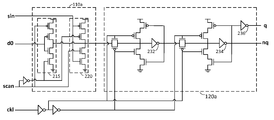
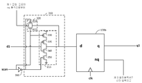
[0028] 도 3은 본 개시의 일 실시예에 따른 스캔 멀티플렉서(310)를 도시한다. 도 3은, 플롭 트레이의 스캔 입력("sin")과 플롭 트레이의 제 1 플립-플롭(120a) 사이에 커플링되는 플롭 트레이의 제 1 스캔 멀티플렉서를 구현하는데 스캔 멀티플렉서(310)가 사용되는 예를 도시한다. 도 3에 도시된 스캔 멀티플렉서(310)를 사용하여 구현되는 스캔 멀티플렉서들을 포함하는 플롭 트레이의 예는 도 5를 참조하여 아래에서 설명된다.[0028] FIG. 3 illustrates a
[0029] 스캔 멀티플렉서(310)에서, 도 2에 도시된 스캔 멀티플렉서(110a)의 제 2 3-상태 회로(220)는 전달 게이트(320)에 의해 대체된다. 전달 게이트(320)는, 제 2 3-상태 회로(220)에 대한 4개의 트랜지스터들과 비교되는 2개의 트랜지스터들을 포함하며, 이는 스캔 멀티플렉서(310) 내에서 2개의 트랜지스터들의 감소를 초래한다. 도 3에 도시된 예에서, 전달 게이트(320)는 병렬로 커플링된 n-타입 트랜지스터(322) 및 p-타입 트랜지스터(324)를 포함하며, 여기서, n-타입 트랜지스터(322)의 게이트는 스캔 모드 입력("scan")에 커플링되고, p-타입 트랜지스터(324)의 게이트는 스캔 모드 인버터(360)를 통해 스캔 모드 입력("scan")에 커플링된다. 따라서, n-타입 트랜지스터(322)의 게이트는 스캔 모드 신호에 의해 드라이빙(drive)되고, p-타입 트랜지스터(324)의 게이트는 스캔 모드 신호의 역에 의해 드라이빙된다. 트랜지스터들(322 및 324) 둘 모두는 스캔 모드에서 턴 온되고, 트랜지스터들(322 및 324) 둘 모두는 정상 모드에서 턴 오프된다.In
[0030] 스캔 모드 신호가 0(정상 모드)인 경우, 제 1 3-상태 회로(215)는 입력 데이터 신호를 인버팅하고, 인버팅된 데이터 신호를 플롭 트레이의 제 1 플립-플롭(120a)의 입력에 출력한다. 제 1 3-상태 회로(215)는 아래에서 더 상세히 설명된다. 전달 게이트(320)는 제 1 D 플립-플롭(120a)의 입력으로부터의 입력 스캔 신호를 차단한다. 따라서, 정상 모드에서, 스캔 멀티플렉서(310)는 도 2에 도시된 제 1 스캔 멀티플렉서(110a)와 기능적으로 동등하다.When the scan mode signal is 0 (normal mode), the first 3-
[0031] 스캔 모드 신호가 1(스캔 모드)인 경우, 제 1 3-상태 회로(215)는 제 1 D 플립-플롭(120a)의 입력으로부터의 입력 데이터 신호를 차단한다. 전달 게이트(320)는 입력 스캔 신호를 제 1 D 플립-플롭(120a)의 입력에 전달한다. 스캔 모드에서, 전달 게이트(320)는, 도 2에 도시된 제 1 멀티플렉서(110a)의 제 2 3-상태 회로(220)와 달리 입력 스캔 신호를 인버팅하지 않는다. 따라서, 스캔 모드에서, 스캔 멀티플렉서(310)는 인버전 없이 스캔 신호를 제 1 플립-플롭(120a)에 전달한다.[0031] When the scan mode signal is 1 (scan mode), the first 3-
[0032] 일 실시예에서, 인버터(315)는, 스캔 멀티플렉서(310)에 입력되기 전에 스캔 신호를 인버팅하기 위해, 플롭 트레이의 스캔 입력("sin")과 스캔 멀티플렉서(310) 사이에 커플링될 수도 있다. 따라서, 스캔 멀티플렉서(310) 내의 전달 게이트(320)와 인버터(315)의 결합은 도 2에 도시된 제 2 3-상태 회로(220)와 기능적으로 동등할 수도 있다.In one embodiment, the
[0033] 플롭 트레이 내의 나머지 스캔 멀티플렉서들 각각은 또한 도 3에 도시된 멀티플렉서(310)를 사용하여 구현될 수 있다. 나머지 스캔 멀티플렉서들 각각에 대해, 전달 게이트(320)의 입력은 개재(intervening) 인버터 없이 앞선 D 플립-플롭의 nq 출력에 커플링될 수도 있다.[0033] Each of the remaining scan multiplexers in the flop tray may also be implemented using the
[0034] 이와 관련하여, 도 4는, 스캔 멀티플렉서(310)가 플롭 트레이 내의 제 2 스캔 멀티플렉서를 구현하는데 사용되는 예를 도시한다. 이러한 예에서, 전달 게이트(320)는 개재 인버터 없이 (도 3에 도시된) 제 1 D 플립-플롭(120a)의 nq 출력에 커플링된다. 위에 설명된 바와 같이, 전달 게이트(320)는 도 2에 도시된 제 2 3-상태 회로(220)를 대체하며, 이는, 멀티플렉서(310) 내에서 2개의 트랜지스터들의 감소를 초래한다.In this regard, FIG. 4 illustrates an example in which the
[0035] 스캔 모드 신호가 0(정상 모드)인 경우, 제 1 3-상태 회로(215)는 입력 데이터 신호를 인버팅하고, 인버팅된 데이터 신호를 플롭 트레이의 제 2 D 플립-플롭(120b)의 입력에 출력한다. 전달 게이트(320)는 제 2 D 플립-플롭(120b)의 입력으로부터의 스캔 신호를 차단한다.When the scan mode signal is 0 (normal mode), the first 3-
[0036] 스캔 모드 신호가 1(스캔 모드)인 경우, 제 1 3-상태 회로(215)는 제 2 D 플립-플롭(120b)의 입력으로부터의 입력 데이터 신호를 차단한다. 전달 게이트(320)는 (도 3에 도시된) 제 1 D 플립-플롭(120a)의 nq 출력으로부터 제 2 D 플립-플롭(120b)의 입력으로 스캔 신호를 전달한다. 제 2 D 플립-플롭(120b)의 nq 출력으로부터의 스캔 신호는 플롭 트레이 내의 제 3 스캔 멀티플렉서에 커플링된다.When the scan mode signal is 1 (scan mode), the first 3-
[0037] 도 5는, 도 1에서의 스캔 회로(115)가 본 개시의 일 실시예에 따른 스캔 회로(515)에 의해 대체되는 스캔가능한 플롭 트레이(500)의 예를 도시한다. 스캔 회로(515)는 제 1 스캔 멀티플렉서(310a), 제 2 스캔 멀티플렉서(310b), 제 3 스캔 멀티플렉서(310c), 및 제 4 스캔 멀티플렉서(310d)를 포함하며, 여기서, 스캔 멀티플렉서들(310a-310d) 각각은 도 3에 도시된 스캔 멀티플렉서(310)를 사용하여 구현된다. 스캔 회로(515)는 또한, 스캔 멀티플렉서들(310a-310d)에 의해 공유되는 스캔 모드 인버터(360)를 포함한다. 스캔 모드 인버터(360)는, 스캔 모드 신호의 역을 각각의 스캔 멀티플렉서(310a-310d)에 제공한다. 플롭 트레이(500)는 또한, 플롭 트레이(500)의 스캔 입력("sin")과 제 1 스캔 멀티플렉서(310a)의 스캔 입력("1"로 라벨링됨) 사이에 커플링되는 인버터(315)를 포함한다.[0037] FIG. 5 illustrates an example of a
[0038] 제 1 스캔 멀티플렉서(310)의 스캔 입력("1"로 라벨링됨)은 인버터(315)에 커플링된다. 나머지 스캔 멀티플렉서들(310b-310d) 각각의 스캔 입력("1"로 라벨링됨)은 개재 인버터 없이 앞선 D 플립-플롭(120a-120c)의 nq 출력에 커플링된다. 스캔 멀티플렉서들(310a-310d) 각각의 데이터 입력("0"으로 라벨링됨)은 개별적인 데이터 신호 d0-d3에 커플링되고, 스캔 멀티플렉서들(310a-310d) 각각의 출력은 개별적인 플립-플롭(120a-120d)의 입력에 커플링된다.[0038] The scan input (labeled "1") of the
[0039] 정상 모드에서, 각각의 스캔 멀티플렉서(310a-310d)는 개별적인 3-상태 회로(215)를 사용하여 개별적인 데이터 신호 d0-d3을 인버팅하고, 인버팅된 데이터 신호를 개별적인 D 플립-플롭(120a-120d)의 입력에 출력한다. 각각의 D 플립-플롭(120a-120d)은 클록 신호 clk의 상승 또는 하강 엣지에서 개별적인 데이터 신호 d0-d3으로부터 데이터 값(예를 들어, 비트)을 캡쳐하고, 캡쳐된 데이터 값 q0-q3을 출력한다.In normal mode, each scan multiplexer 310a-310d inverts the individual data signals d0-d3 using separate three-
[0040] 스캔 모드에서, 인버터(315)는, 인버팅된 입력 스캔 신호를 생성하기 위해, 플롭 트레이(500)의 스캔 입력("sin")에서의 스캔 신호를 인버팅한다. 제 1 스캔 멀티플렉서(310a)는 인버팅된 입력 스캔 신호를 제 1 D 플립-플롭(120a)의 입력에 전달한다. 나머지 스캔 멀티플렉서들(310b-310c) 각각은, 앞선 플립-플롭(120a-120c)으로부터의 스캔 신호 출력을 인버전 없이 개별적인 플립-플롭(120b-120d)의 입력에 커플링시킨다. 스캔 신호는 최종적으로, NAND 게이트(130)의 출력("sout"으로 라벨링됨)에서 출력된다. 출력 스캔 신호는, 플롭 트레이(500)의 스캔 입력("sin")으로부터 스캔 출력("sout")까지의 스캔 경로 내의 인버전들의 개수에 의존하여, 입력 스캔 신호에 대해 인버팅될 수도 있거나 또는 넌-인버팅될 수도 있다. [0040] In scan mode,
[0041] 따라서, 스캔 모드에서, 스캔 신호는 플롭 트레이(500)의 D 플립-플롭들(120a-120d)을 통해 스캔된다. 스캔 신호는 알려진 테스트 패턴을 포함할 수도 있고, 플롭 트레이(500)의 기능은, 알려진 테스트 패턴에 기초하여, 플롭 트레이(500)로부터의 출력 스캔 신호를 기대되는 출력 스캔 신호와 비교함으로써 평가될 수도 있다. 도 5에서의 플롭 트레이(500)에 대한 기대되는 출력 스캔 신호는, 주어진 테스트 패턴에 대해, 도 1에서의 플롭 트레이(100)에 대한 기대되는 출력 스캔 신호와 상이할 수도 있다. 이것은, 도 5에서의 플롭 트레이(500)가 스캔 경로에서 상이한 개수의 인버전들을 갖기 때문에, 스캔 멀티플렉서들(310a-310d)이 스캔 신호를 인버팅하지 않는다는 사실로 인해서이다.Thus, in the scan mode, the scan signal is scanned through the D flip-flops 120a-120d of the
[0042] 도 3에 도시된 멀티플렉서(310)를 사용하여 플롭 트레이(500)의 각각의 스캔 멀티플렉서(310a-310d)를 구현하는 것은, 플롭 트레이(500) 내의 트랜지스터들의 개수에서 상당한 감소를 유도할 수 있다. 플롭 트레이(500) 내의 제 1 스캔 멀티플렉서(310a)는, 플롭 트레이(500)의 스캔 입력("sin")과 제 1 스캔 멀티플렉서(310a) 사이에 커플링된 인버터(315) 때문에, 트랜지스터들의 개수에서의 감소에 기여하지 않을 수도 있다. 그러나, 플롭 트레이(500) 내의 나머지 스캔 멀티플렉서들(310b-310d)은 각각은 트랜지스터 수를 2개만큼 감소시킨다. 이것은, 나머지 스캔 멀티플렉서들(310b-310d) 각각에 대해, 개별적인 전달 게이트(320)가 도 2에 도시된 제 2 3-상태 회로(220)에 대한 4개의 트랜지스터들과 비교하여 2개의 트랜지스터들을 사용하기 때문이다. 예를 들어, 4-비트 플롭 트레이(도 5에 도시된 예)에 대해, 이것은 도 1에서의 플롭 트레이(100)와 비교하여 6개의 트랜지스터들의 감소(3개의 나머지 멀티플렉서들(310b-310d) 각각에 대해 2개의 트랜지스터의 감소)를 유도한다. 8개의 D 플립-플롭들을 포함하는 8-비트 플롭 트레이에 대해 이것은 14개의 트랜지스터들의 감소를 유도하며, 16개의 D 플립-플롭들을 포함하는 16-비트 플롭 트레이에 대해 이것은 30개의 트랜지스터들의 감소를 유도한다. 스캔 회로(515) 내의 트랜지스터들의 개수의 감소는 스캔 회로에 의해 차지되는 칩 영역을 감소시키고 전력 소모를 감소시킨다.Implementing each scan multiplexer 310a-310d of the
[0043] 각각의 D 플립-플롭(120a-120d)이 자신의 입력에서의 신호(예를 들어, 개별적인 데이터 신호 d0-d3 또는 스캔 신호)로부터 값을 적절히 캡쳐하기 위해, 값은 클록 clk의 상승 또는 하강 엣지 이후의 시간 기간에 대해 안정될 필요가 있다(유지 시간(hold time)으로 지칭됨). 신호가 유지 시간 동안 값을 변경하는 경우, 유지 시간 위반(violation)이 발생하고 플립-플롭은 준안정 상태로 진입할 수도 있다. 정상 모드에서 유지 시간 위반을 방지하기 위해, 플립-플롭의 입력에서 충분한 유지 시간 마진(margin)을 제공하도록 플립-플롭으로의 데이터 경로에서의 지연이 조절될 수도 있다. 유지 시간 마진은, 클록 clk의 상승 또는 하강 엣지 이후 신호에서의 변경에 대해 기대되는 시간과 유지 시간 사이의 차이일 수도 있다. 더 큰 유지 시간 마진은 프로세스 및 동작 변화들에 대해 더 큰 마진을 제공함으로써, 플립-플롭의 강건성(robustness)을 개선한다.In order for each D flip-
[0044] 스캔 모드에서, 도 5에서의 제 2, 제 3, 및 제 4 플립-플롭들(120b-120d) 각각에 대한 유지 시간 마진은, 도 1에서의 제 2, 제 3, 및 제 4 플립-플롭들들(120b-120d)과 비교하여 대략적으로 하나의 인버터 지연만큼 감소된다. 이것은, 도 5에서의 개별적인 멀티플렉서들(310b-310d) 각각이 도 1에서의 개별적인 멀티플렉서들(110b-110d)과 달리 스캔 신호를 인버팅하지 않기 때문이다. 그러나, 스캔 모드에서의 유지 시간 마진의 감소에도 불구하고, 유지 시간 마진은 테스팅 동안 유지 시간 위반들을 방지하기에 충분할 만큼 크게 유지될 수도 있다. 예를 들어, 플립-플롭들(120b-120d) 각각이 도 2에 도시된 플립-플롭을 사용하여 구현되는 경우, 스캔 모드에서의 유지 시간 마진이 유지 시간 위반들을 방지하기에 충분할 만큼 크게 유지된다는 것이 발견된다. 제 1 플립-플롭(120a)에 대한 유지 시간 마진은, 제 1 멀티플렉서(110a)에 커플링된 인버터(315)가 인버터 지연을 부가하기 때문에 대략적으로 동일할 수도 있다.In the scan mode, the hold time margins for each of the second, third, and fourth flip-
[0045] 도 3을 다시 참조하여 이제 제 1 3-상태 회로(215)가 더 상세히 설명될 것이다. 제 1 3-상태 회로(215)는 3-상태 인버터의 예이고, 제 1 p-타입 트랜지스터(330), 제 2 p-타입 트랜지스터(335), 제 1 n-타입 트랜지스터(350), 및 제 2 n-타입 트랜지스터(340)를 포함한다. 트랜지스터들(330, 335, 340, 및 350)은, 전력 공급부와 접지 사이에서 다른 트랜지스터의 상단 상에 적층(stack)된다. 더 구체적으로는, 제 1 p-타입 트랜지스터(330) 소스는 전력 공급부에 커플링되고, 제 2 p-타입 트랜지스터(335)의 소스는 제 1 p-타입 트랜지스터(330)의 드레인에 커플링되고, 제 2 n-타입 트랜지스터(340)의 드레인은 제 2 p-타입 트랜지스터(335)의 드레인에 커플링되고, 제 1 n-타입 트랜지스터(350)의 드레인은 제 2 n-타입 트랜지스터(340)의 소스에 커플링되고, 제 1 n-타입 트랜지스터(350)의 소스는 접지에 커플링된다.[0045] Referring back to FIG. 3, the first 3-
[0046] 제 1 p-타입 트랜지스터(330)의 게이트는 스캔 모드 입력("scan")에 커플링되고, 제 1 n-타입 트랜지스터(350)의 게이트는, 도 5에 도시된 바와 같이, 스캔 멀티플렉서들(310a-310d)에 의해 공유될 수도 있는 스캔 모드 인버터(360)를 통해 스캔 모드 입력("scan")에 커플링된다. 따라서, 제 1 p-타입 트랜지스터(330)의 게이트는 스캔 모드 신호에 의해 드라이빙되고, 제 1 n-타입 트랜지스터(350)의 게이트는 스캔 모드 신호의 역에 의해 드라이빙된다. 제 2 p-타입 트랜지스터(335) 및 제 2 n-타입 트랜지스터(340)의 게이트들은 멀티플렉서(310)의 데이터 입력에 커플링된다.The gate of the first p-
[0047] 스캔 모드 신호가 0(정상 모드)인 경우, 제 1 p-타입 트랜지스터(330) 및 제 1 n-타입 트랜지스터(350) 둘 모두는 턴 온된다. 결과적으로, 제 1 p-타입 트랜지스터(330)는 제 2 p-타입 트랜지스터(335)의 소스를 전력 공급부에 커플링시키고, 제 1 n-타입(350)은 제 2 n-타입 트랜지스터(340)의 소스를 접지에 커플링시킨다. 이것은, 제 2 p-타입 트랜지스터(335)와 제 2 n-타입 트랜지스터(340)가 상보형 인버터로서 동작하는 것을 가능하게 하며, 여기서, 인버터의 입력은 제 2 p-타입 트랜지스터(335) 및 제 2 n-타입 트랜지스터(340)의 게이트들에 로케이팅(locate)되고, 인버터의 출력은 제 2 p-타입 트랜지스터(335) 및 제 2 n-타입 트랜지스터(340)의 드레인들에 로케이팅된다. 인버터는, 개별적인 데이터 신호를 인버팅하고, 인버팅된 데이터 신호를 개별적인 플립-플롭에 출력한다.When the scan mode signal is 0 (normal mode), both the first p-
[0048] 스캔 모드 신호가 1(스캔 모드)인 경우, 제 1 p-타입 트랜지스터(330) 및 제 1 n-타입 트랜지스터(350) 둘 모두는 턴 오프된다. 이것은, 제 2 p-타입 트랜지스터(335)의 소스를 전력 공급부로부터 분리시키고, 제 2 n-타입 트랜지스터(340)의 소스를 접지로부터 분리시킨다. 결과적으로, 개별적인 플립-플롭의 입력으로부터의 개별적인 데이터 신호는 차단된다.When the scan mode signal is 1 (scan mode), both the first p-
[0049] 도 6은 본 개시의 일 실시예에 따른, 감소된 스캔 오버헤드로 플롭 트레이를 스캔하기 위한 방법(600)의 흐름도이다.[0049] FIG. 6 is a flow diagram of a
[0050] 단계(610)에서, 정상 모드에서, 3-상태 회로를 사용하여 입력 데이터 신호가 인버팅되고 플립-플롭의 입력에 출력된다. 예를 들어, 단계(610)는 도 3에서의 3-상태 회로(215)를 사용하여 수행될 수도 있으며, 여기서, 3-상태 회로(215)는, 0의 스캔 모드 신호를 스캔 모드 입력("scan")에 입력함으로써 정상 모드에서 동작된다.[0050] In
[0051] 단계(620)에서, 스캔 모드에서, 3-상태 회로를 사용하여 플립-플롭의 입력으로부터의 입력 데이터 신호가 차단된다. 예를 들어, 단계(620)는 도 3에서의 3-상태 회로(215)를 사용하여 수행될 수도 있으며, 여기서, 3-상태 회로(215)는, 1의 스캔 모드 신호를 스캔 모드 입력("scan")에 입력함으로써 스캔 모드에서 동작된다.[0051] In
[0052] 단계(630)에서, 스캔 모드에서, 전달 게이트를 사용하여 스캔 신호가 플립-플롭의 입력에 전달된다. 예를 들어, 단계(630)는 도 3에서의 전달 게이트(320)를 사용하여 수행될 수도 있으며, 여기서, 전달 게이트(320)는, 1의 스캔 모드 신호를 스캔 모드 입력("scan")에 입력함으로써 스캔 모드에서 동작된다. 전달 게이트(320)는 3-상태 회로보다 더 적은 트랜지스터들을 사용하여 구현될 수도 있으며, 그에 따라 스캔 오버헤드를 감소시킨다.[0052] In
[0053] 단계(640)에서, 정상 모드에서, 전달 게이트를 사용하여 플립-플롭의 입력으로부터의 스캔 신호가 차단된다. 예를 들어, 단계(640)는 도 3에서의 전달 게이트(320)를 사용하여 수행될 수도 있으며, 여기서, 전달 게이트(320)는, 0의 스캔 모드 신호를 스캔 모드 입력("scan")에 입력함으로써 정상 모드에서 동작된다.[0053] In
[0054] 당업자들은, 본 개시의 실시예들이 본 명세서에 설명된 예들로 제한되지 않는다는 것을 인식할 것이다. 예를 들어, 스캔 멀티플렉서의 스캔 입력은 nq 출력 대신 앞선 플립-플롭의 q 출력에 커플링될 수도 있다. 또한, 본 개시의 실시예들은, 다양한 타입들의 플립-플롭들을 포함하는 플롭 트레이들에서 사용될 수도 있으며, 따라서, 도 2에 도시된 예시적인 플립-플롭들로 제한되지 않는다. 추가로, 본 개시의 실시예들은, 예를 들어, 2개의 플립-플롭들, 4개의 플립-플롭들, 8개의 플립-플롭들, 16개의 플립-플롭들 등을 포함하는 임의의 개수의 플립-플롭들을 포함하는 플롭 트레이들에서 사용될 수도 있다.[0054] Those skilled in the art will recognize that the embodiments of the present disclosure are not limited to the examples described herein. For example, the scan input of the scan multiplexer may be coupled to the q output of the previous flip-flop instead of the nq output. In addition, the embodiments of the present disclosure may be used in flop trays comprising various types of flip-flops and are therefore not limited to the exemplary flip-flops shown in Fig. In addition, embodiments of the present disclosure may include any number of flip-flops including, for example, two flip-flops, four flip-flops, eight flip-flops, sixteen flip- - flops. ≪ / RTI >
[0055] 당업자들은, 본 명세서에 설명된 회로들이 다양한 트랜지스터 타입들을 사용하여 실현될 수도 있으며, 따라서 도면들에 도시된 특정한 트랜지스터 타입들로 제한되지 않는다는 것을 인식할 것이다. 예를 들어, 양극성 접합 트랜지스터(bipolar junction transistor)들, 접합형 전계 효과 트랜지스터(junction field effect transistor) 또는 임의의 다른 트랜지스터 타입과 같은 트랜지스터 타입들이 사용될 수도 있다. 당업자들은 또한, 본 명세서에 설명된 회로들이 COMS, BJT(bipolar junction transistor), BiCMOS(bipolar-CMOS), SiGe(silicon germanium), GaAs(gallium arsenide) 등과 같은 다양한 IC 프로세스 기술들로 제조될 수도 있다는 것을 인식할 것이다.[0055] Those skilled in the art will recognize that the circuits described herein may be implemented using various transistor types, and thus are not limited to the particular transistor types shown in the Figures. For example, transistor types such as bipolar junction transistors, junction field effect transistors, or any other transistor type may be used. Those skilled in the art will also appreciate that the circuits described herein may be fabricated with various IC process technologies such as COMS, bipolar junction transistors (BJTs), bipolar-CMOS (BiCMOS), silicon germanium (SiGe), gallium arsenide ≪ / RTI >
[0056] 본 개시의 이전 설명은 임의의 당업자가 본 개시를 사용 또는 실시할 수 있도록 제공된다. 본 개시에 대한 다양한 변형들은 당업자들에게 용이하게 명백할 것이며, 본 명세서에 정의된 일반적인 원리들은 본 개시의 사상 또는 범위로부터 벗어나지 않으면서 다른 변형들에 적용될 수도 있다. 따라서, 본 개시는 본 명세서에 설명된 예들로 제한되도록 의도되는 것이 아니라, 본 명세서에 기재된 원리들 및 신규한 특성들과 일치하는 가장 넓은 범위에 부합할 것이다.[0056] The previous description of the disclosure is provided to enable any person skilled in the art to make or use the disclosure. Various modifications to the disclosure will be readily apparent to those skilled in the art, and the generic principles defined herein may be applied to other variations without departing from the spirit or scope of the disclosure. Accordingly, this disclosure is not intended to be limited to the examples described herein, but is to be accorded the widest scope consistent with the principles and novel features disclosed herein.
Claims (22)
정상 모드에서, 입력 데이터 신호를 인버팅(invert)하여 인버팅된 데이터 신호를 플립-플롭(flip-flop)의 입력에 출력하고, 스캔 모드에서, 상기 플롭 트레이의 상기 플립-플롭의 입력으로부터의 데이터 신호를 차단하도록 구성되는 3-상태(tri-state) 회로; 및
스캔 모드에서, 상기 플립-플롭의 입력에 스캔 신호를 전달하고, 정상 모드에서, 상기 플립-플롭의 입력으로부터의 스캔 신호를 차단하도록 구성되는 전달 게이트를 포함하는, 플롭 트레이에 대한 스캔 회로.A scan circuit for a flop tray,
In normal mode, inverting an input data signal to output an inverted data signal to an input of a flip-flop, and in scan mode, from an input of the flip-flop of the flop tray A tri-state circuit configured to block the data signal; And
And a transfer gate configured to transfer a scan signal to an input of the flip-flop in a scan mode and to block a scan signal from an input of the flip-flop in a normal mode.
상기 전달 게이트는,
n-타입 트랜지스터; 및
상기 n-타입 트랜지스터와 병렬로 커플링되는 p-타입 트랜지스터를 포함하며,
상기 p-타입 트랜지스터 및 상기 n-타입 트랜지스터는 스캔 모드에서 턴 온(turn on)되고 정상 모드에서 턴 오프(turn off)되도록 구성되는, 플롭 트레이에 대한 스캔 회로.The method according to claim 1,
The transfer gate includes:
n-type transistors; And
And a p-type transistor coupled in parallel with the n-type transistor,
Wherein the p-type transistor and the n-type transistor are configured to be turned on in a scan mode and turned off in a normal mode.
상기 플롭 트레이의 스캔 입력과 상기 전달 게이트 사이에 커플링되는 인버터를 더 포함하는, 플롭 트레이에 대한 스캔 회로.The method according to claim 1,
Further comprising an inverter coupled between the scan input of the flop tray and the transfer gate.
상기 전달 게이트는, 상기 플롭 트레이의 다른 플립-플롭의 출력과 상기 플립-플롭의 입력 사이에 커플링되는, 플롭 트레이에 대한 스캔 회로.The method according to claim 1,
Wherein the transfer gate is coupled between an output of another flip-flop of the flop tray and an input of the flip-flop.
상기 다른 플립-플롭의 출력과 상기 전달 게이트 사이에 어떠한 인버터도 존재하지 않는, 플롭 트레이에 대한 스캔 회로.5. The method of claim 4,
Wherein no inverter is present between the output of the other flip-flop and the transfer gate.
정상 모드에서, 제 1 데이터 신호를 인버팅하여 인버팅된 제 1 데이터 신호를 상기 플롭 트레이의 제 1 플립-플롭의 입력에 출력하고, 스캔 모드에서, 상기 제 1 플립-플롭의 입력으로부터의 제 1 데이터 신호를 차단하도록 구성되는 제 1 3-상태 회로;
스캔 모드에서, 상기 제 1 플립-플롭의 입력에 스캔 신호를 전달하고, 정상 모드에서, 상기 제 1 플립-플롭의 입력으로부터의 스캔 신호를 차단하도록 구성되는 제 1 전달 게이트;
정상 모드에서, 제 2 데이터 신호를 인버팅하여 인버팅된 제 2 데이터 신호를 상기 플롭 트레이의 제 2 플립-플롭의 입력에 출력하고, 스캔 모드에서, 상기 제 2 플립-플롭의 입력으로부터의 제 2 데이터 신호를 차단하도록 구성되는 제 2 3-상태 회로; 및
스캔 모드에서, 상기 제 1 플립-플롭의 출력으로부터 상기 제 2 플립-플롭의 입력으로 상기 스캔 신호를 전달하고, 정상 모드에서, 상기 제 1 플립-플롭의 출력으로부터 상기 제 2 플립-플롭의 입력으로의 스캔 신호를 차단하도록 구성되는 제 2 전달 게이트를 포함하는, 플롭 트레이에 대한 스캔 회로.A scan circuit for a flop tray,
In a normal mode, a first data signal is inverted to output an inverted first data signal to an input of a first flip-flop of the flop tray, and in a scan mode, a first data signal from an input of the first flip- A first three-state circuit configured to block one data signal;
A first transfer gate configured to transfer a scan signal to an input of the first flip-flop in a scan mode and to block a scan signal from an input of the first flip-flop in a normal mode;
In a normal mode, a second data signal is inverted to output an inverted second data signal to an input of a second flip-flop of the flop tray, and in scan mode, a second data signal from the input of the second flip- A second 3-state circuit configured to block the 2 data signal; And
Flop from the output of the first flip-flop to the input of the second flip-flop in a scan mode, and in normal mode, transfers the scan signal from the output of the first flip-flop to the input of the second flip- And a second transfer gate configured to interrupt the scan signal to the scan line.
상기 제 1 플립-플롭의 출력과 상기 제 2 전달 게이트 사이에 어떠한 인버터도 존재하지 않는, 플롭 트레이에 대한 스캔 회로.The method according to claim 6,
Wherein no inverter is present between the output of the first flip-flop and the second transfer gate.
상기 플롭 트레이의 스캔 입력과 상기 제 1 전달 게이트 사이에 커플링된 인버터를 더 포함하는, 플롭 트레이에 대한 스캔 회로The method according to claim 6,
Further comprising an inverter coupled between the scan input of the flop tray and the first transfer gate, the scan circuit for the flop tray
상기 제 1 플립-플롭의 출력과 상기 제 2 전달 게이트 사이에 어떠한 인버터도 존재하지 않는, 플롭 트레이에 대한 스캔 회로9. The method of claim 8,
And wherein no inverter is present between the output of the first flip-flop and the second transfer gate,
상기 제 2 전달 게이트는,
n-타입 트랜지스터; 및
상기 n-타입 트랜지스터와 병렬로 커플링되는 p-타입 트랜지스터를 포함하며,
상기 p-타입 트랜지스터 및 상기 n-타입 트랜지스터는 스캔 모드에서 턴 온되고 정상 모드에서 턴 오프되도록 구성되는, 플롭 트레이에 대한 스캔 회로.10. The method of claim 9,
The second transmission gate includes:
n-type transistors; And
And a p-type transistor coupled in parallel with the n-type transistor,
Wherein the p-type transistor and the n-type transistor are configured to be turned on in a scan mode and turned off in a normal mode.
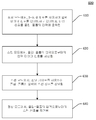
정상 모드에서, 3-상태 회로를 사용하여, 입력 데이터 신호를 인버팅하고 인버팅된 데이터 신호를 상기 플롭 트레이의 플립-플롭의 입력에 출력하는 단계;
스캔 모드에서, 상기 3-상태 회로를 사용하여, 상기 플립-플롭의 입력으로부터의 데이터 신호를 차단하는 단계;
스캔 모드에서, 전달 게이트를 사용하여, 스캔 신호를 상기 플립-플롭의 입력에 전달하는 단계; 및
정상 모드에서, 상기 전달 게이트를 사용하여, 상기 플립-플롭의 입력으로부터의 스캔 신호를 차단하는 단계를 포함하는, 플롭 트레이를 스캔하기 위한 방법.CLAIMS 1. A method for scanning a flop tray,
In normal mode, using a three-state circuit, inverting the input data signal and outputting the inverted data signal to the input of the flip-flop of the flop tray;
Blocking the data signal from the input of the flip-flop, using the 3-state circuit, in scan mode;
Transferring a scan signal to an input of the flip-flop using a transfer gate in a scan mode; And
And in a normal mode, using the transfer gate to interrupt a scan signal from an input of the flip-flop.
스캔 모드에서, 다른 전달 게이트를 사용하여, 상기 플립-플롭으로부터 출력된 스캔 신호를 상기 플롭 트레이의 다른 플립-플롭의 입력에 전달하는 단계를 더 포함하는, 플롭 트레이를 스캔하기 위한 방법.12. The method of claim 11,
Transferring the scan signal output from the flip-flop to an input of another flip-flop in the flop tray, using a different transfer gate in scan mode.
상기 플립-플롭으로부터 출력된 스캔 신호는, 상기 플립-플롭으로부터 출력된 스캔 신호를 인버팅함이 없이 상기 다른 플립-플롭의 입력에 전달되는, 플롭 트레이를 스캔하기 위한 방법.13. The method of claim 12,
Wherein the scan signal output from the flip-flop is transferred to the input of the other flip-flop without inverting the scan signal output from the flip-flop.
상기 전달 게이트를 사용하여 상기 스캔 신호를 상기 플립-플롭의 입력에 전달하기에 앞서, 상기 스캔 신호를 인버팅하는 단계를 더 포함하는, 플롭 트레이를 스캔하기 위한 방법.12. The method of claim 11,
Further comprising inverting the scan signal prior to transferring the scan signal to the input of the flip-flop using the transfer gate.
스캔 모드에서, 다른 전달 게이트를 사용하여, 상기 플립-플롭으로부터 출력된 스캔 신호를 상기 플롭 트레이의 다른 플립-플롭의 입력에 전달하는 단계를 더 포함하는, 플롭 트레이를 스캔하기 위한 방법.15. The method of claim 14,
Transferring the scan signal output from the flip-flop to an input of another flip-flop in the flop tray, using a different transfer gate in scan mode.
상기 플립-플롭으로부터 출력된 스캔 신호는, 상기 플립-플롭으로부터 출력된 스캔 신호를 인버팅함이 없이 상기 다른 플립-플롭의 입력에 전달되는, 플롭 트레이를 스캔하기 위한 방법.16. The method of claim 15,
Wherein the scan signal output from the flip-flop is transferred to the input of the other flip-flop without inverting the scan signal output from the flip-flop.
정상 모드에서, 입력 데이터 신호를 인버팅하여 인버팅된 데이터 신호를 상기 플롭 트레이의 플립-플롭의 입력에 출력하기 위한 수단;
스캔 모드에서, 상기 플립-플롭의 입력으로부터의 데이터 신호를 차단하기 위한 수단;
스캔 모드에서, 스캔 신호를 상기 플립-플롭의 입력에 전달하기 위한 수단; 및
정상 모드에서, 상기 플립-플롭의 입력으로부터의 스캔 신호를 차단하기 위한 수단을 포함하는, 플롭 트레이를 스캔하기 위한 장치.An apparatus for scanning a flop tray,
Means for inverting an input data signal to output an inverted data signal to an input of a flip-flop of the flop tray, in a normal mode;
Means for interrupting a data signal from an input of the flip-flop in a scan mode;
Means for transferring a scan signal to an input of the flip-flop; And
And means for interrupting a scan signal from an input of the flip-flop in a normal mode.
스캔 모드에서, 상기 플립-플롭으로부터 출력된 스캔 신호를 상기 플롭 트레이의 다른 플립-플롭의 입력에 전달하기 위한 수단을 더 포함하는, 플롭 트레이를 스캔하기 위한 장치.18. The method of claim 17,
Means for transferring the scan signal output from the flip-flop to an input of another flip-flop in the flop tray in a scan mode.
상기 플립-플롭으로부터 출력된 스캔 신호는, 상기 플립-플롭으로부터 출력된 스캔 신호를 인버팅함이 없이 상기 다른 플립-플롭의 입력에 전달되는, 플롭 트레이를 스캔하기 위한 장치.19. The method of claim 18,
Wherein the scan signal output from the flip-flop is transferred to the input of the other flip-flop without inverting the scan signal output from the flip-flop.
상기 스캔 신호를 상기 플립-플롭의 입력에 전달하기 위한 수단 이전에, 상기 스캔 신호를 인버팅하기 위한 수단을 더 포함하는, 플롭 트레이를 스캔하기 위한 장치.18. The method of claim 17,
Further comprising means for inverting the scan signal prior to the means for transferring the scan signal to the input of the flip-flop.
스캔 모드에서, 상기 플립-플롭으로부터 출력된 스캔 신호를 상기 플롭 트레이의 다른 플립-플롭의 입력에 전달하기 위한 수단을 더 포함하는, 플롭 트레이를 스캔하기 위한 장치.21. The method of claim 20,
Means for transferring the scan signal output from the flip-flop to an input of another flip-flop in the flop tray in a scan mode.
상기 플립-플롭으로부터 출력된 스캔 신호는, 상기 플립-플롭으로부터 출력된 스캔 신호를 인버팅함이 없이 상기 다른 플립-플롭의 입력에 전달되는, 플롭 트레이를 스캔하기 위한 장치.22. The method of claim 21,
Wherein the scan signal output from the flip-flop is transferred to the input of the other flip-flop without inverting the scan signal output from the flip-flop.
Applications Claiming Priority (3)
| Application Number | Priority Date | Filing Date | Title |
|---|---|---|---|
| US13/905,060 US9024658B2 (en) | 2013-05-29 | 2013-05-29 | Circuit and layout techniques for flop tray area and power otimization |
| US13/905,060 | 2013-05-29 | ||
| PCT/US2014/039856 WO2014193998A1 (en) | 2013-05-29 | 2014-05-28 | Circuit and layout techniques for flop tray area and power optimization |
Publications (1)
| Publication Number | Publication Date |
|---|---|
| KR20160016890A true KR20160016890A (en) | 2016-02-15 |
Family
ID=51022458
Family Applications (1)
| Application Number | Title | Priority Date | Filing Date |
|---|---|---|---|
| KR1020157036440A KR20160016890A (en) | 2013-05-29 | 2014-05-28 | Circuit and layout techniques for flop tray area and power optimization |
Country Status (6)
| Country | Link |
|---|---|
| US (1) | US9024658B2 (en) |
| EP (1) | EP3004903B1 (en) |
| JP (1) | JP6337099B2 (en) |
| KR (1) | KR20160016890A (en) |
| CN (1) | CN105247377B (en) |
| WO (1) | WO2014193998A1 (en) |
Cited By (1)
| Publication number | Priority date | Publication date | Assignee | Title |
|---|---|---|---|---|
| KR20220080661A (en) * | 2020-12-07 | 2022-06-14 | 타이완 세미콘덕터 매뉴팩쳐링 컴퍼니 리미티드 | Circuit screening system and circuit screening method |
Families Citing this family (5)
| Publication number | Priority date | Publication date | Assignee | Title |
|---|---|---|---|---|
| JP6268461B2 (en) | 2013-03-28 | 2018-01-31 | セイコーエプソン株式会社 | Semiconductor device, physical quantity sensor, electronic device and mobile object |
| US9685141B2 (en) * | 2014-01-31 | 2017-06-20 | Samsung Display Co., Ltd. | MDLL/PLL hybrid design with uniformly distributed output phases |
| US10033359B2 (en) | 2015-10-23 | 2018-07-24 | Qualcomm Incorporated | Area efficient flip-flop with improved scan hold-margin |
| US9966953B2 (en) | 2016-06-02 | 2018-05-08 | Qualcomm Incorporated | Low clock power data-gated flip-flop |
| US11092646B1 (en) * | 2020-02-18 | 2021-08-17 | Qualcomm Incorporated | Determining a voltage and/or frequency for a performance mode |
Family Cites Families (32)
| Publication number | Priority date | Publication date | Assignee | Title |
|---|---|---|---|---|
| US5444404A (en) | 1994-03-03 | 1995-08-22 | Vlsi Technology, Inc. | Scan flip-flop with power saving feature |
| WO1995030230A2 (en) * | 1994-04-28 | 1995-11-09 | Apple Computer, Inc. | Scannable d-flip-flop with system independent clocking |
| JPH09270677A (en) * | 1995-09-05 | 1997-10-14 | Mitsubishi Electric Corp | Flip-flop circuit, scanning path and storage circuit |
| US5719878A (en) | 1995-12-04 | 1998-02-17 | Motorola Inc. | Scannable storage cell and method of operation |
| JPH1052073A (en) * | 1996-07-31 | 1998-02-20 | Seiko Kurotsuku Kk | Drive circuit for ultrasonic motor |
| JPH1194914A (en) | 1997-09-22 | 1999-04-09 | Matsushita Electric Ind Co Ltd | Scan path control circuit |
| US6708303B1 (en) | 1998-03-06 | 2004-03-16 | Texas Instruments Incorporated | Method and apparatus for controlling a seperate scan output of a scan circuit |
| US6289477B1 (en) * | 1998-04-28 | 2001-09-11 | Adaptec, Inc. | Fast-scan-flop and integrated circuit device incorporating the same |
| US6420894B1 (en) | 1999-12-29 | 2002-07-16 | Intel Corporation | Implementation of iscan cell for self-resetting dynamic circuit |
| JP3928938B2 (en) * | 2002-05-28 | 2007-06-13 | シャープ株式会社 | Voltage conversion circuit and semiconductor device |
| JP2004069492A (en) * | 2002-08-06 | 2004-03-04 | Renesas Technology Corp | Flip-flop circuit |
| US7237164B1 (en) | 2004-04-15 | 2007-06-26 | Marvell International Ltd. | Area optimized edge-triggered flip-flop for high-speed memory dominated design |
| JP2006005661A (en) * | 2004-06-17 | 2006-01-05 | Matsushita Electric Ind Co Ltd | Flip-flop circuit |
| KR101076809B1 (en) * | 2004-06-18 | 2011-10-25 | 삼성전자주식회사 | Scan flip-flop circuit to reduce redundant power consumption |
| US20060085707A1 (en) * | 2004-09-28 | 2006-04-20 | Texas Instruments Incorporated | High speed energy conserving scan architecture |
| KR100604904B1 (en) | 2004-10-02 | 2006-07-28 | 삼성전자주식회사 | Flip flop circuit with Scan input |
| US7315191B2 (en) * | 2005-06-30 | 2008-01-01 | Texas Instruments Incorporated | Digital storage element architecture comprising dual scan clocks and reset functionality |
| US7543205B2 (en) * | 2006-04-27 | 2009-06-02 | Texas Instruments Incorporated | Control signal synchronization of a scannable storage circuit |
| US7793178B2 (en) | 2006-07-12 | 2010-09-07 | Texas Instruments Incorporated | Cell supporting scan-based tests and with reduced time delay in functional mode |
| US7649395B2 (en) | 2007-05-15 | 2010-01-19 | Ati Technologies Ulc | Scan flip-flop with internal latency for scan input |
| JP4999632B2 (en) * | 2007-10-12 | 2012-08-15 | オンセミコンダクター・トレーディング・リミテッド | Semiconductor integrated circuit |
| KR20090131010A (en) * | 2008-06-17 | 2009-12-28 | 주식회사 동부하이텍 | Dual mode edge triggered flip-flop |
| US7893722B2 (en) * | 2008-09-11 | 2011-02-22 | Arm Limited | Clock control of state storage circuitry |
| CN102062836B (en) * | 2009-11-17 | 2013-02-06 | 三星半导体(中国)研究开发有限公司 | Scan register, scan chain, and chip and test method thereof |
| US20110181331A1 (en) * | 2010-01-24 | 2011-07-28 | Freescale Semiconductor, Inc. | Integrated circuit with leakage reduction in static nets |
| US8427214B2 (en) * | 2010-06-03 | 2013-04-23 | Arm Limited | Clock state independent retention master-slave flip-flop |
| CN103004088B (en) * | 2010-07-16 | 2016-04-13 | 马维尔国际贸易有限公司 | Charge injection sense amplifier |
| US8493119B2 (en) * | 2010-12-13 | 2013-07-23 | Apple Inc. | Scannable flip-flop with hold time improvements |
| US8502561B2 (en) * | 2011-07-01 | 2013-08-06 | Arm Limited | Signal value storage circuitry with transition detector |
| US8578224B2 (en) * | 2011-12-31 | 2013-11-05 | Texas Instruments Incorporated | High density flip-flop with asynchronous reset |
| CN103576082B (en) * | 2012-08-06 | 2018-01-12 | 恩智浦美国有限公司 | Low-power sweep trigger unit |
| US9020084B2 (en) * | 2013-01-31 | 2015-04-28 | Qualcomm Incorporated | High frequency synchronizer |
-
2013
- 2013-05-29 US US13/905,060 patent/US9024658B2/en active Active
-
2014
- 2014-05-28 JP JP2016516796A patent/JP6337099B2/en active Active
- 2014-05-28 KR KR1020157036440A patent/KR20160016890A/en not_active Application Discontinuation
- 2014-05-28 WO PCT/US2014/039856 patent/WO2014193998A1/en active Application Filing
- 2014-05-28 EP EP14733455.1A patent/EP3004903B1/en active Active
- 2014-05-28 CN CN201480030877.3A patent/CN105247377B/en active Active
Cited By (1)
| Publication number | Priority date | Publication date | Assignee | Title |
|---|---|---|---|---|
| KR20220080661A (en) * | 2020-12-07 | 2022-06-14 | 타이완 세미콘덕터 매뉴팩쳐링 컴퍼니 리미티드 | Circuit screening system and circuit screening method |
Also Published As
| Publication number | Publication date |
|---|---|
| EP3004903B1 (en) | 2017-05-03 |
| US9024658B2 (en) | 2015-05-05 |
| JP2016531275A (en) | 2016-10-06 |
| WO2014193998A1 (en) | 2014-12-04 |
| CN105247377B (en) | 2018-02-09 |
| EP3004903A1 (en) | 2016-04-13 |
| US20140359385A1 (en) | 2014-12-04 |
| CN105247377A (en) | 2016-01-13 |
| JP6337099B2 (en) | 2018-06-06 |
Similar Documents
| Publication | Publication Date | Title |
|---|---|---|
| KR20160016890A (en) | Circuit and layout techniques for flop tray area and power optimization | |
| US8566658B2 (en) | Low-power and area-efficient scan cell for integrated circuit testing | |
| US8880965B2 (en) | Low power scan flip-flop cell | |
| US8484523B2 (en) | Sequential digital circuitry with test scan | |
| EP2151051B1 (en) | Scan flip-flop with internal latency for scan input | |
| US20090300448A1 (en) | Scan flip-flop device | |
| US7859310B2 (en) | Semiconductor integrated circuit | |
| US20090309641A1 (en) | Dual mode edge triggered flip-flop | |
| US20110260767A1 (en) | System and device for reducing instantaneous voltage droop during a scan shift operation | |
| US9020084B2 (en) | High frequency synchronizer | |
| US9081061B1 (en) | Scan flip-flop | |
| JP3535855B2 (en) | Scan flip-flop and semiconductor integrated circuit device | |
| US7501850B1 (en) | Scannable limited switch dynamic logic (LSDL) circuit | |
| US20090083595A1 (en) | Scan test circuit | |
| CN106409342B (en) | Area efficient multi-bit flip-flop topology | |
| JP3573703B2 (en) | Method for manufacturing semiconductor device | |
| US7512856B2 (en) | Register circuit, scanning register circuit utilizing register circuits and scanning method thereof | |
| JP5231065B2 (en) | Scan flip-flop circuit | |
| US6492841B2 (en) | Integrated NAND and flip-flop circuit | |
| JP2019036622A (en) | Storage circuit and control method of the same | |
| US20110320896A1 (en) | Integrated Circuit Devices Having Selectively Enabled Scan Paths With Power Saving Circuitry | |
| JP2008058246A (en) | Semiconductor integrated circuit, test circuit disposed in semiconductor integrated circuit, and test method used for semiconductor integrated circuit |
Legal Events
| Date | Code | Title | Description |
|---|---|---|---|
| WITN | Application deemed withdrawn, e.g. because no request for examination was filed or no examination fee was paid |