JP6337099B2 - Circuit and layout techniques for flop tray area and power optimization - Google Patents
Circuit and layout techniques for flop tray area and power optimization Download PDFInfo
- Publication number
- JP6337099B2 JP6337099B2 JP2016516796A JP2016516796A JP6337099B2 JP 6337099 B2 JP6337099 B2 JP 6337099B2 JP 2016516796 A JP2016516796 A JP 2016516796A JP 2016516796 A JP2016516796 A JP 2016516796A JP 6337099 B2 JP6337099 B2 JP 6337099B2
- Authority
- JP
- Japan
- Prior art keywords
- flop
- flip
- scan
- input
- type transistor
- Prior art date
- Legal status (The legal status is an assumption and is not a legal conclusion. Google has not performed a legal analysis and makes no representation as to the accuracy of the status listed.)
- Active
Links
Images


Classifications
-
- G—PHYSICS
- G01—MEASURING; TESTING
- G01R—MEASURING ELECTRIC VARIABLES; MEASURING MAGNETIC VARIABLES
- G01R31/00—Arrangements for testing electric properties; Arrangements for locating electric faults; Arrangements for electrical testing characterised by what is being tested not provided for elsewhere
- G01R31/28—Testing of electronic circuits, e.g. by signal tracer
- G01R31/317—Testing of digital circuits
- G01R31/3177—Testing of logic operation, e.g. by logic analysers
-
- G—PHYSICS
- G01—MEASURING; TESTING
- G01R—MEASURING ELECTRIC VARIABLES; MEASURING MAGNETIC VARIABLES
- G01R31/00—Arrangements for testing electric properties; Arrangements for locating electric faults; Arrangements for electrical testing characterised by what is being tested not provided for elsewhere
- G01R31/28—Testing of electronic circuits, e.g. by signal tracer
- G01R31/317—Testing of digital circuits
- G01R31/3181—Functional testing
- G01R31/3185—Reconfiguring for testing, e.g. LSSD, partitioning
- G01R31/318533—Reconfiguring for testing, e.g. LSSD, partitioning using scanning techniques, e.g. LSSD, Boundary Scan, JTAG
- G01R31/318541—Scan latches or cell details
Description
[0001]本開示の態様は、一般に走査可能フロップトレイ(flop tray)に関し、より詳細には、走査可能フロップトレイの走査オーバーヘッドを低減することに関する。 [0001] Aspects of the present disclosure relate generally to scanable flop trays and, more particularly, to reducing the scan overhead of a scannable flop tray.
[0002]フリップフロップは、システムの様々な構成要素による処理のために1つまたは複数のデータ信号からデータ値をキャプチャ(ラッチ)するためにシステムにおいて使用され得る。システムは、フリップフロップがテスト中に正しく機能していることを検証するための走査回路を含み得る。これを行うために、走査回路は、既知のテストパターンを有する走査信号を受信し、フリップフロップを通して走査信号を走査する。走査信号がフリップフロップを通して走査された後、出力走査信号は、フリップフロップが正しく機能しているかどうかを決定するために、予想される出力走査信号と比較される。予想される出力走査信号は、入力走査信号の既知のテストパターンと、フリップフロップの予想される機能とに基づき得る。走査回路は、走査回路よって消費されるチップ面積および/電力により、システムにオーバーヘッドを追加する。 [0002] Flip-flops can be used in a system to capture (latch) data values from one or more data signals for processing by various components of the system. The system may include a scanning circuit for verifying that the flip-flop is functioning correctly during the test. To do this, the scanning circuit receives a scanning signal having a known test pattern and scans the scanning signal through a flip-flop. After the scan signal is scanned through the flip-flop, the output scan signal is compared to the expected output scan signal to determine if the flip-flop is functioning correctly. The expected output scan signal may be based on the known test pattern of the input scan signal and the expected function of the flip-flop. The scanning circuit adds overhead to the system due to the chip area and / or power consumed by the scanning circuit.
[0003]以下で、1つまたは複数の実施形態の基本的理解を与えるために、そのような実施形態の簡略化された概要を提示する。この概要は、すべての企図された実施形態の包括的な概観ではなく、すべての実施形態の主要または重要な要素を識別するものでも、いずれかまたはすべての実施形態の範囲を定めるものでもない。その唯一の目的は、後で提示するより詳細な説明の導入として、1つまたは複数の実施形態のいくつかの概念を簡略化された形で提示することである。 [0003] The following presents a simplified overview of such embodiments to provide a basic understanding of one or more embodiments. This summary is not an exhaustive overview of all contemplated embodiments, nor is it intended to identify key or critical elements of all embodiments or delineate the scope of any or all embodiments. Its sole purpose is to present some concepts of one or more embodiments in a simplified form as a prelude to the more detailed description that is presented later.
[0004]一態様によれば、フロップトレイのための走査回路が提供される。本走査回路は、通常モードで入力データ信号を反転させ、反転したデータ信号をフロップトレイのフリップフロップの入力に出力することと、走査モードでデータ信号をフリップフロップの入力から遮断することとを行うように構成されたトライステート回路(tri-state circuit)を備える。本走査回路はまた、走査モードで走査信号をフリップフロップの入力にパスすることと、通常モードで走査信号をフリップフロップの入力から遮断することとを行うように構成されたパスゲート(pass gate)を備える。 [0004] According to one aspect, a scanning circuit for a flop tray is provided. The scanning circuit inverts the input data signal in the normal mode, outputs the inverted data signal to the input of the flip-flop of the flop tray, and blocks the data signal from the input of the flip-flop in the scanning mode. A tri-state circuit configured as described above. The scanning circuit also includes a pass gate configured to pass the scanning signal to the flip-flop input in the scanning mode and to block the scanning signal from the input of the flip-flop in the normal mode. Prepare.
[0005]第2の態様はフロップトレイのための走査回路に関する。本走査回路は、通常モードで第1のデータ信号を反転させ、反転した第1のデータ信号をフロップトレイの第1のフリップフロップの入力に出力することと、走査モードで第1のデータ信号を第1のフリップフロップの入力から遮断することとを行うように構成された第1のトライステート回路を備える。本走査回路はまた、走査モードで走査信号を第1のフリップフロップの入力にパスすることと、通常モードで走査信号を第1のフリップフロップの入力から遮断することとを行うように構成された第1のパスゲートを備える。本走査回路はまた、通常モードで第2のデータ信号を反転させ、反転した第2のデータ信号をフロップトレイの第2のフリップフロップの入力に出力することと、走査モードで第2のデータ信号を第2のフリップフロップの入力から遮断することとを行うように構成された第2のトライステート回路を備える。本回路は、さらに、走査モードで第1のフリップフロップの出力からの走査信号を第2のフリップフロップの入力にパスすることと、通常モードで第1のフリップフロップの出力からの走査信号を第2のフリップフロップの入力から遮断することとを行うように構成された第2のパスゲートを備える。 [0005] A second aspect relates to a scanning circuit for a flop tray. The scanning circuit inverts the first data signal in the normal mode, outputs the inverted first data signal to the input of the first flip-flop of the flop tray, and outputs the first data signal in the scanning mode. A first tri-state circuit configured to shut off from an input of the first flip-flop. The scanning circuit is also configured to pass the scanning signal to the input of the first flip-flop in the scanning mode and to block the scanning signal from the input of the first flip-flop in the normal mode. A first pass gate is provided. The scanning circuit also inverts the second data signal in the normal mode, outputs the inverted second data signal to the input of the second flip-flop of the flop tray, and the second data signal in the scanning mode. A second tri-state circuit configured to shut off from the input of the second flip-flop. The circuit further passes the scan signal from the output of the first flip-flop in scan mode to the input of the second flip-flop and the scan signal from the output of the first flip-flop in normal mode. A second pass gate configured to shut off from the input of the second flip-flop.
[0006]第3の態様は、フロップトレイを走査するための方法に関する。本方法は、トライステート回路を使用して通常モードで入力データ信号を反転させ、反転したデータ信号をフロップトレイのフリップフロップの入力に出力することと、トライステート回路を使用して走査モードでデータ信号をフリップフロップの入力から遮断することとを備える。本方法はまた、パスゲートを使用して走査モードで走査信号をフリップフロップの入力にパスすることと、パスゲートを使用して通常モードで走査信号をフリップフロップの入力から遮断することとを備える。 [0006] A third aspect relates to a method for scanning a flop tray. This method uses a tristate circuit to invert the input data signal in the normal mode, outputs the inverted data signal to the input of the flip-flop of the flop tray, and uses the tristate circuit to scan the data in the scan mode. Shutting off the signal from the input of the flip-flop. The method also comprises using a pass gate to pass the scan signal to the input of the flip-flop in scan mode and using the pass gate to block the scan signal from the input of the flip-flop in normal mode.
[0007]第4の態様は、フロップトレイを走査するための装置に関する。本装置は、通常モードで入力データ信号を反転させ、反転したデータ信号をフロップトレイのフリップフロップの入力に出力するための手段と、走査モードでデータ信号をフリップフロップの入力から遮断するための手段とを備える。本装置はまた、走査モードで走査信号をフリップフロップの入力にパスするための手段と、通常モードで走査信号をフリップフロップの入力から遮断するための手段とを備える。 [0007] A fourth aspect relates to an apparatus for scanning a flop tray. The apparatus has means for inverting the input data signal in the normal mode and outputting the inverted data signal to the input of the flip-flop of the flop tray, and means for blocking the data signal from the input of the flip-flop in the scanning mode. With. The apparatus also includes means for passing the scan signal to the input of the flip-flop in the scan mode and means for blocking the scan signal from the input of the flip-flop in the normal mode.
[0008]上記および関連する目的を達成するために、1つまたは複数の実施形態は、以下で十分に説明し、特許請求の範囲で具体的に指摘する特徴を備える。以下の説明および添付の図面に、1つまたは複数の実施形態のいくつかの例示的な態様を詳細に示す。ただし、これらの態様は、様々な実施形態の原理が採用され得る様々な方法のほんのいくつかを示すものであり、説明する実施形態は、すべてのそのような態様およびそれらの均等物を含むものとする。 [0008] To the accomplishment of the above and related ends, one or more embodiments comprise the features fully described below and specifically pointed out in the claims. The following description and the annexed drawings set forth in detail certain illustrative aspects of the one or more embodiments. However, these aspects are merely illustrative of the various ways in which the principles of the various embodiments may be employed, and the described embodiments are intended to include all such aspects and their equivalents. .
[0015]添付の図面に関して以下に記載する発明を実施するための形態は、様々な構成を説明するものであり、本明細書で説明する概念が実施され得る唯一の構成を表すものではない。発明を実施するための形態は、様々な概念の完全な理解を与えるための具体的な詳細を含む。ただし、これらの概念はこれらの具体的な詳細なしに実施され得ることが当業者には明らかであろう。いくつかの例では、そのような概念を曖昧にするのを回避するために、よく知られている構造および構成要素をブロック図の形態で示す。 [0015] The detailed description set forth below in connection with the appended drawings is intended as a description of various configurations and is not intended to represent the only configurations in which the concepts described herein may be implemented. The detailed description includes specific details for providing a thorough understanding of various concepts. However, it will be apparent to those skilled in the art that these concepts may be practiced without these specific details. In some instances, well-known structures and components are shown in block diagram form in order to avoid obscuring such concepts.
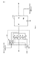
[0016]図1に、走査可能フロップトレイ100の一例を示す。フロップトレイ100は通常モードまたは走査モードで動作することができる。フロップトレイ100は、フロップトレイ100の正しい機能をテストするために、テスト中に走査モードで動作させられる。
FIG. 1 illustrates an example of a
[0017]フロップトレイ100は、第1のDフリップフロップ120aと、第2のDフリップフロップ120bと、第3のDフリップフロップ120cと、第4のDフリップフロップ120dと、走査回路115とを備える。走査回路115は、以下でさらに説明するように、テスト中に走査モードでフロップトレイ100を動作させるために使用される。走査回路115は、第1の走査マルチプレクサ110aと、第2の走査マルチプレクサ110bと、第3の走査マルチプレクサ110cと、第4の走査マルチプレクサ110dと、反転極性NANDゲート130とを備える。各走査マルチプレクサ110a〜110dはDフリップフロップ120a〜120dの各々に結合され、ここにおいて、第1の走査マルチプレクサ110aは第1のDフリップフロップ120aの入力に結合され、第2の走査マルチプレクサ110bは第2のDフリップフロップ120bの入力に結合され、以下同様に結合される。走査回路115はフロップトレイ100の走査オーバーヘッドとなる。
The
[0018]通常モードで、フロップトレイ100は複数のデータ信号d0〜d3を並列に受信する。各走査マルチプレクサ110a〜110dは、(図1中で「0」と標示された)データ入力において並列データ信号d0〜d3のうちの1つを受信し、それぞれのデータ信号d0〜d3をそれぞれのDフリップフロップ120a〜120dの入力にパスする。各Dフリップフロップ120a〜120dは、クロック信号clkの立上りまたは立下りエッジ上でそれぞれのデータ信号d0〜d3からデータ値(たとえば、ビット)をキャプチャし、キャプチャされたデータ値q0〜q3を出力する。したがって、各クロックサイクル中に、フロップトレイ100は、クロック信号clkの立上りまたは立下りエッジ上でデータ信号d0〜d3から複数のデータ値(たとえば、ビット)を並列にキャプチャし、キャプチャされたデータ値q0〜q3を並列に出力する。図1は、4つのフリップフロップを備える4ビットフロップトレイの例を示す。しかしながら、本開示はこの例に限定されず、任意の数のフリップフロップを備えるフロップトレイに適用され得ることを諒解されたい。
[0018] In the normal mode, the
[0019]走査モードで、第1の走査マルチプレクサ110aは、(図1中で「sin」と標示された)フロップトレイ100の走査入力を第1のフリップフロップ120aの入力に結合する。残りの走査マルチプレクサ110b〜110dの各々は前のDフリップフロップのnq出力をそれぞれのDフリップフロップの入力に結合する。たとえば、第2の走査マルチプレクサ110bは第1のDフリップフロップ120aのnq出力を第2のDフリップフロップ120bの入力に結合し、第3のマルチプレクサ110cは第2のDフリップフロップ120bのnq出力を第3のDフリップフロップ120cの入力に結合し、以下同様に結合する。各マルチプレクサの走査入力は図1中で「1」と標示されている。第4のDフリップフロップ120d(最後のフリップフロップ)のnq出力はNANDゲート130の反転入力に結合される。その結果、走査信号が走査入力(「sin」)においてフロップトレイ100に入力されたとき、走査信号はフロップトレイ100のDフリップフロップ120a〜120dを通って連続的に伝搬する。走査信号は(「sout」と標示された)NANDゲート130の出力において最終的に出力される。出力走査信号は、フロップトレイ100の走査入力(「sin」)から走査出力(「sout」)までの走査経路における反転の回数に応じて、入力走査信号に対して反転または非反転であり得る。
[0019] In scan mode, the
[0020]したがって、走査モードで、走査信号はフロップトレイ100のDフリップフロップ120a〜120dを通って走査される。走査信号は既知のテストパターンを備え得、フロップトレイ100の機能は、フロップトレイ100からの出力走査信号を既知のテストパターンに基づく予想される出力走査信号と比較することによって評価され得る。
[0020] Thus, in the scan mode, the scan signal is scanned through the D flip-flops 120a-120d of the
[0021]図1に示された例では、フロップトレイ100の動作モードは、(図1中で「scan」と標示された)走査モード入力において受信された走査モード信号によって制御される。走査モード信号は、走査マルチプレクサがそれぞれのフリップフロップにそれぞれの入力データ信号を結合するのか走査信号を結合するのかを制御するために、各走査マルチプレクサ110a〜110dに入力される。たとえば、走査モード信号が論理0であるとき、各走査マルチプレクサ110a〜110dはそれぞれの入力データ信号をそれぞれのフリップフロップに結合する。したがって、フロップトレイは、走査モード信号が0であるとき、通常モードで動作する。走査モード信号が論理1であるとき、各走査マルチプレクサ110a〜110dは走査信号をそれぞれのフリップフロップに結合する。したがって、フロップトレイは、走査モード信号が1であるとき、走査モードで動作する。走査モード信号はまた、図1に示されているように、NANDゲート130の非反転入力に結合され得る。走査モード信号が0であるとき(通常モード)、NANDゲート130の出力は1に固定される。
[0021] In the example shown in FIG. 1, the operating mode of the
[0022]図2に、第1の走査マルチプレクサ110aおよび第1のDフリップフリップ120aの例示的な実装形態を示す。第1の走査マルチプレクサ110aは第1のトライステート回路215と第2のトライステート回路220とを備え、ここにおいて、各トライステート回路は4つのトランジスタ(たとえば、金属酸化物半導体(MOS)トランジスタ)を含む。第1のトライステート回路215および第2のトライステート回路220は、(図2中で「scan」と標示された)走査モード入力において受信された走査モード信号によって制御される。トライステート回路215および220は、走査モード信号が0であるとき、通常モードで動作し、走査モード信号が1であるとき、走査モードで動作する。
[0022] FIG. 2 illustrates an exemplary implementation of the
[0023]走査モード信号が0であるとき、第1のトライステート回路215はそれぞれの入力データ信号を反転させ、第2のトライステート回路220は反転したデータ信号をそれぞれのDフリップフロップ120aの入力にパスする。図2中の例では、Dフリップフロップ120aはそれの入力とq出力との間に奇数個のインバータ(すなわち、インバータ232、234および236)を有する。奇数個のインバータは第1のトライステート回路215による論理反転を元に戻す。その結果、マルチプレクサ110aのデータ入力からDフリップフロップ120aのq出力まで論理反転がない。
[0023] When the scan mode signal is 0, the first
[0024]走査モード信号が1であるとき、第1のトライステート回路215はそれぞれのデータ入力を遮断する。第2のトライステート回路220は、それぞれの入力走査信号を反転させ、反転した走査信号をそれぞれのDフリップフロップ120aに入力する。図2中の例では、Dフリップフロップ120aはそれの入力とnq出力との間に偶数個のインバータ(すなわち、インバータ232および234)を有する。その結果、マルチプレクサ110aの走査入力からDフリップフロップ120aのnq出力まで論理反転がある。
[0024] When the scan mode signal is 1, the first
[0025]したがって、通常モードで、図2中の走査マルチプレクサ110aは、データ信号をそれぞれのフリップフロップ120aに出力する前に、入力データ信号を反転させる。走査モードで、走査マルチプレクサ110aは、走査信号をそれぞれのフリップフロップ120aに出力する前に、入力走査信号を反転させる。したがって、図2中の走査マルチプレクサ110aは反転マルチプレクサの例である。
[0025] Thus, in normal mode, the
[0026]フロップトレイ100中の残りの走査マルチプレクサ110b〜110dの各々はまた、図2に示された回路を使用して実装され得る。残りの走査マルチプレクサ110b〜110dの各々について、(図1中で「1」と標示された)マルチプレクサの走査入力は前のDフリップフロップ120a〜120cのnq出力に結合される。
[0026] Each of the remaining scan multiplexers 110b-110d in the
[0027]各走査マルチプレクサ110a〜110dの第1のトライステート回路215および第2のトライステート回路220を構成するトランジスタは、チップ面積を占め、電力を消費する。したがって、走査回路115の面積および/または電力消費を低減するために、マルチプレクサ中のトランジスタの数を低減することが望ましい。
[0027] The transistors that make up the first
[0028]図3に、本開示の一実施形態による、走査マルチプレクサ310を示す。図3は、走査マルチプレクサ310が、フロップトレイの走査入力(「sin」)とフロップトレイの第1のフリップフロップ120aとの間に結合された、フロップトレイ中の第1の走査マルチプレクサを実装するために使用される例を示す。図3に示された走査マルチプレクサ310を使用して実装された走査マルチプレクサを含むフロップトレイの一例について、以下で図5に関して説明する。
[0028] FIG. 3 illustrates a
[0029]走査マルチプレクサ310では、図2に示された走査マルチプレクサ110a中の第2のトライステート回路220はパスゲート320によって置き換えられる。パスゲート320は、第2のトライステート回路220のための4つのトランジスタと比較して2つのトランジスタを備え、走査マルチプレクサ310中の2つのトランジスタの低減を生じる。図3に示された例では、パスゲート320は、並列に結合されたn形トランジスタ322とp形トランジスタ324とを備え、ここにおいて、n形トランジスタ322のゲートは走査モード入力(「scan」)に結合され、p形トランジスタ324のゲートは走査モードインバータ360を通して走査モード入力(「scan」)に結合される。したがって、n形トランジスタ322のゲートは走査モード信号によって駆動され、p形トランジスタ324のゲートは走査モード信号の逆によって駆動される。トランジスタ322とトランジスタ324の両方は走査モードでオンにされ、トランジスタ322とトランジスタ324の両方は通常モードでオフにされる。
[0029] In
[0030]走査モード信号が0であるとき(通常モード)、第1のトライステート回路215は、入力データ信号を反転させ、反転したデータ信号をフロップトレイの第1のフリップフロップ120aの入力に出力する。第1のトライステート回路215について以下でより詳細に説明する。パスゲート320は入力走査信号を第1のDフリップフロップ120aの入力から遮断する。したがって、通常モードで、走査マルチプレクサ310は、図2に示された第1の走査マルチプレクサ110aと機能的に等価である。
[0030] When the scanning mode signal is 0 (normal mode), the first
[0031]走査モード信号が1であるとき(走査モード)、第1のトライステート回路215は入力データ信号を第1のDフリップフロップ120aの入力から遮断する。パスゲート320は入力走査信号を第1のDフリップフロップ120aの入力にパスする。走査モードで、パスゲート320は、図2に示された第1のマルチプレクサ110a中の第2のトライステート回路220とは異なり、入力走査信号を反転させない。したがって、走査モードで、走査マルチプレクサ310は反転なしに走査信号を第1のフリップフロップ120aにパスする。
[0031] When the scan mode signal is 1 (scan mode), the first
[0032]一実施形態では、インバータ315は、走査マルチプレクサ310に入力されることより前に走査信号を反転させるために、フロップトレイの走査入力(「sin」)と走査マルチプレクサ310との間に結合され得る。したがって、インバータ315と走査マルチプレクサ310中のパスゲート320の組合せは、図2に示された第2のトライステート回路220と機能的に等価であり得る。
[0032] In one embodiment,
[0033]フロップトレイ中の残りの走査マルチプレクサの各々はまた、図3に示されたマルチプレクサ310を使用して実装され得る。残りの走査マルチプレクサの各々について、パスゲート320の入力は介在インバータなしに前のDフリップフロップのnq出力に結合され得る。
[0033] Each of the remaining scanning multiplexers in the flop tray may also be implemented using the
[0034]この点について、図4に、走査マルチプレクサ310が、フロップトレイ中の第2の走査マルチプレクサを実装するために使用される例を示す。この例では、パスゲート320は介在インバータなしに(図3に示された)第1のDフリップフロップ120aのnq出力に結合される。上記で説明したように、パスゲート320は図2に示された第2のトライステート回路220を置き換え、マルチプレクサ310中の2つのトランジスタの低減を生じる。
[0034] In this regard, FIG. 4 shows an example where
[0035]走査モード信号が0であるとき(通常モード)、第1のトライステート回路215は、入力データ信号を反転させ、反転したデータ信号をフロップトレイの第2のDフリップフロップ120bの入力に出力する。パスゲート320は走査信号を第2のDフリップフロップ120bの入力から遮断する。
[0035] When the scanning mode signal is 0 (normal mode), the first
[0036]走査モード信号が1であるとき(走査モード)、第1のトライステート回路215は入力データ信号を第2のDフリップフロップ120bの入力から遮断する。パスゲート320は走査信号を(図3に示された)第1のDフリップフロップ120aのnq出力から第2のDフリップフロップ120bの入力にパスする。第2のDフリップフロップ120bのnq出力からの走査信号はフロップトレイ中の第3の走査マルチプレクサに結合される。
[0036] When the scan mode signal is 1 (scan mode), the first
[0037]図5に、走査可能フロップトレイ500の例を示し、ここにおいて、図1中の走査回路115は、本開示の一実施形態による走査回路515によって置き換えられる。走査回路515は、第1の走査マルチプレクサ310aと、第2の走査マルチプレクサ310bと、第3の走査マルチプレクサ310cと、第4の走査マルチプレクサ310dとを備え、ここにおいて、走査マルチプレクサ310a〜310dの各々は、図3に示された走査マルチプレクサ310を使用して実装される。走査回路515はまた、走査マルチプレクサ310a〜310dによって共有される走査モードインバータ360を備える。走査モードインバータ360は各走査マルチプレクサ310a〜310dに走査モード信号の逆を与える。フロップトレイ500はまた、フロップトレイ500の走査入力(「sin」)と第1の走査マルチプレクサ310aの(「1」と標示された)走査入力との間に結合されたインバータ315を備える。
[0037] FIG. 5 illustrates an example of a
[0038]第1の走査マルチプレクサ310の(「1」と標示された)走査入力はインバータ315に結合される。残りの走査マルチプレクサ310b〜310dの各々の(「1」と標示された)走査入力は、介在インバータなしに前のDフリップフロップ120a〜120cのnq出力に結合される。走査マルチプレクサ310a〜310dの各々の(「0」と標示された)データ入力はそれぞれのデータ信号d0〜d3に結合され、走査マルチプレクサ310a〜310dの各々の出力はそれぞれのフリップフロップ120a〜120dの入力に結合される。
[0038] The scan input (labeled “1”) of the
[0039]通常モードで、各走査マルチプレクサ310a〜310dは、それぞれのトライステート回路215を使用してそれぞれのデータ信号d0〜d3を反転させ、反転したデータ信号をそれぞれのDフリップフロップ120a〜120dの入力に出力する。各Dフリップフロップ120a〜120dは、クロック信号clkの立上りまたは立下りエッジ上でそれぞれのデータ信号d0〜d3からデータ値(たとえば、ビット)をキャプチャし、キャプチャされたデータ値q0〜q3を出力する。
[0039] In the normal mode, each of the scanning multiplexers 310a-310d uses the respective
[0040]走査モードで、インバータ315は、反転した入力走査信号を生成するためにフロップトレイ500の走査入力(「sin」)において走査信号を反転させる。第1の走査マルチプレクサ310aは反転した入力走査信号を第1のDフリップフロップ120aの入力にパスする。残りの走査マルチプレクサ310b〜310cの各々は、前のフリップフロップ120a〜120cから出力された走査信号を反転なしにそれぞれのフリップフロップ120b〜120dの入力に結合する。走査信号は(「sout」と標示された)NANDゲート130の出力において最終的に出力される。出力走査信号は、フロップトレイ500の走査入力(「sin」)から走査出力(「sout」)までの走査経路における反転の回数に応じて、入力走査信号に対して反転または非反転であり得る。
[0040] In the scan mode,
[0041]したがって、走査モードで、走査信号はフロップトレイ500のDフリップフロップ120a〜120dを通って走査される。走査信号は既知のテストパターンを備え得、フロップトレイ500の機能は、フロップトレイ500からの出力走査信号を既知のテストパターンに基づく予想される出力走査信号と比較することによって評価され得る。所与のテストパターンについて、図5中のフロップトレイ500の場合の予想される出力走査信号は、図1中のフロップトレイ100の場合の予想される出力走査信号とは異なり得る。これは、走査マルチプレクサ310a〜310dが走査信号を反転させないという事実により、図5中のフロップトレイ500が走査経路における異なる回数の反転を有するからである。
[0041] Accordingly, in the scan mode, the scan signal is scanned through the D flip-flops 120a-120d of the
[0042]図3に示されたマルチプレクサ310を使用してフロップトレイ500の各走査マルチプレクサ310a〜310dを実装することは、フロップトレイ500中のトランジスタの数の有意な低減をもたらし得る。フロップトレイ500中の第1の走査マルチプレクサ310aは、フロップトレイ500の走査入力(「sin」)と第1の走査マルチプレクサ310aとの間に結合されたインバータ315のために、トランジスタの数の低減に寄与しないことがある。しかしながら、フロップトレイ500中の残りの走査マルチプレクサ310b〜310dの各々はトランジスタの数を2だけ低減する。これは、残りの走査マルチプレクサ310b〜310dの各々のために、それぞれのパスゲート320は、図2に示された第2のトライステート回路220のための4つのトランジスタと比較して2つのトランジスタを使用するからである。たとえば、(その一例が図5に示された)4ビットフロップトレイの場合、これは図1中のフロップトレイ100と比較して6つのトランジスタの低減(3つの残りのマルチプレクサ310b〜310dの各々について2つのトランジスタの低減)をもたらす。8つのDフリップフロップを備える8ビットフロップトレイの場合、これは14個のトランジスタの低減をもたらし、16個のDフリップフロップを備える16ビットフロップトレイの場合、これは30個のトランジスタの低減をもたらす。走査回路515中のトランジスタの数の低減は、走査回路によって占められるチップ面積を低減し、電力消費を低減する。
[0042] Implementing each scan multiplexer 310a-310d of the
[0043]各Dフリップフロップ120a〜120dがそれの入力において信号(たとえば、それぞれのデータ信号d0〜d3または走査信号)から値を適切にキャプチャするために、値は(ホールド時間と呼ばれる)クロックclkの立上りまたは立下りエッジの後のある時間期間の間安定必要がある。信号がホールド時間中に値を変更した場合、ホールド時間違反が起こり、フリップフロップは準安定状態に入り得る。通常モードでのホールド時間違反を防ぐために、フリップフロップへのデータ経路における遅延が、フリップフロップの入力において十分なホールド時間マージンを与えるために調整され得る。ホールド時間マージンは、クロックclkの立上りまたは立下りエッジの後の信号の変化についての予想される時間とホールド時間との間の差であり得る。より大きいホールド時間マージンは、より大きいマージンをプロセスおよび動作変動に与えることによってフリップフロップのロバストネスを改善する。
[0043] In order for each D flip-
[0044]走査モードで、図5中の第2のフリップフロップ120b、第3のフリップフロップ120cおよび第4のフリップフロップ120dの各々のためのホールド時間マージンは、図1中の第2のフリップフロップ120b、第3のフリップフロップ120cおよび第4のフリップフロップ120dと比較して約1つのインバータ遅延だけ低減される。これは、図5中のそれぞれのマルチプレクサ310b〜310dの各々が、図1中のそれぞれのマルチプレクサ110b〜110dとは異なり走査信号を反転させないからである。しかしながら、走査モードにおけるホールド時間マージンの低減の場合でも、ホールド時間マージンは、テスト中のホールド時間違反を防ぐのに十分に大きいままであり得る。たとえば、フリップフロップ120b〜120dの各々が図2に示されたフリップフロップを使用して実装されたとき、走査モードにおけるホールド時間マージンはホールド時間違反を防ぐほど十分に大きいままであることが分かっている。第1のフリップフロップ120aのためのホールド時間マージンは、第1のマルチプレクサ110aに結合されたインバータ315がインバータ遅延を追加するのでほぼ同じであり得る。
[0044] In scan mode, the hold time margin for each of second flip-
[0045]次に、再び図3を参照しながら、第1のトライステート回路215についてより詳細に説明する。第1のトライステート回路215は、トライステートインバータの一例であり、第1のp形トランジスタ330と、第2のp形トランジスタ335と、第1のn形トランジスタ350と、第2のn形トランジスタ340とを備える。トランジスタ330、335、340および350は電源と接地との間で互いの上に積層される。より詳細には、第1のp形トランジスタ330のソースは電源に結合され、第2のp形トランジスタ335のソースは第1のp形トランジスタ330のドレインに結合され、第2のn形トランジスタ340のドレインは第2のp形トランジスタ335のドレインに結合され、第1のn形トランジスタ350のドレインは第2のn形トランジスタ340のソースに結合され、第1のn形トランジスタ350のソースは接地に結合される。
[0045] Next, the first
[0046]第1のp形トランジスタ330のゲートは走査モード入力(「scan」)に結合され、第1のn形トランジスタ350のゲートは、図5に示されているように走査マルチプレクサ310a〜310dによって共有され得る、走査モードインバータ360を通して走査モード入力(「scan」)に結合される。したがって、第1のp形トランジスタ330のゲートは走査モード信号によって駆動され、第1のn形トランジスタ350のゲートは走査モード信号の逆によって駆動される。第2のp形トランジスタ335および第2のn形トランジスタ340のゲートはマルチプレクサ310のデータ入力に結合される。
[0046] The gate of the first p-
[0047]走査モード信号が0であるとき(通常モード)、第1のp形トランジスタ330と第1のn形トランジスタ350は両方ともオンにされる。その結果、第1のp形トランジスタ330は第2のp形トランジスタ335のソースを電源に結合し、第1のn形350は第2のn形トランジスタ340のソースを接地に結合する。これは、第2のp形トランジスタ335および第2のn形トランジスタ340がコンプリメンタリーインバータとして働くことを可能にし、ここにおいて、インバータの入力は第2のp形トランジスタ335および第2のn形トランジスタ340のゲートに位置し、インバータの出力は第2のp形トランジスタ335および第2のn形トランジスタ340のドレインに位置する。インバータは、それぞれのデータ信号を反転させ、反転したデータ信号をそれぞれのフリップフロップに出力する。
[0047] When the scan mode signal is 0 (normal mode), both the first p-
[0048]走査モード信号が1であるとき(走査モード)、第1のp形トランジスタ330と第1のn形トランジスタ350は両方ともオフにされる。これは、第2のp形トランジスタ335のソースを電源から切断し、第2のn形トランジスタ340のソースを接地から切断する。その結果、それぞれのデータ信号はそれぞれのフリップフロップの入力から遮断される。
[0048] When the scan mode signal is 1 (scan mode), both the first p-
[0049]図6は、本開示の一実施形態による、低減された走査オーバーヘッドをもつフロップトレイを走査するための方法600の流れ図である。
[0049] FIG. 6 is a flow diagram of a
[0050]ステップ610において、入力データ信号は、トライステート回路を使用して通常モードで反転させられ、フリップフロップの入力に出力される。たとえば、ステップ610は、図3中のトライステート回路215を使用して実行され得、ここにおいて、トライステート回路215は、0の走査モード信号を走査モード入力(「scan」)に入力することによって通常モードで動作させられる。
[0050] In
[0051]ステップ620において、入力データ信号は、トライステート回路を使用して走査モードでフリップフロップの入力から遮断される。たとえば、ステップ620は、図3中のトライステート回路215を使用して実行され得、ここにおいて、トライステート回路215は、1の走査モード信号を走査モード入力(「scan」)に入力することによって走査モードで動作させられる。
[0051] In
[0052]ステップ630において、走査信号は、パスゲートを使用して走査モードでフリップフロップの入力にパスされる。たとえば、ステップ630は、図3中のパスゲート320を使用して実行され得、ここにおいて、パスゲート320は、1の走査モード信号を走査モード入力(「scan」)に入力することによって走査モードで動作させられる。パスゲート320は、トライステート回路よりも少数のトランジスタを使用して実装され、したがって走査オーバーヘッドを低減し得る。
[0052] In
[0053]ステップ640において、走査信号は、パスゲートを使用して通常モードでフリップフロップの入力から遮断される。たとえば、ステップ640は、図3中のパスゲート320を使用して実行され得、ここにおいて、パスゲート320は、0の走査モード信号を走査モード入力(「scan」)に入力することによって通常モードで動作させられる。
[0053] At
[0054]当業者は、本開示の実施形態が本明細書で説明した例に限定されないことを諒解されよう。たとえば、走査マルチプレクサの走査入力は、nq出力の代わりに前のフリップフロップのq出力に結合され得る。また、本開示の実施形態は、様々なタイプのフリップフロップを備えるフロップトレイ中で使用され得、したがって、図2に示された例示的なフリップフロップに限定されない。さらに、本開示の実施形態は、たとえば、2つのフリップフロップ、4つのフリップフロップ、8つのフリップフロップ、16個のフリップフロップなどを含む、任意の数のフリップフロップを備えるフロップトレイ中で使用され得る。 [0054] Those skilled in the art will appreciate that embodiments of the present disclosure are not limited to the examples described herein. For example, the scan input of the scan multiplexer can be coupled to the q output of the previous flip-flop instead of the nq output. Also, embodiments of the present disclosure can be used in flop trays with various types of flip-flops, and thus are not limited to the exemplary flip-flop shown in FIG. Further, embodiments of the present disclosure may be used in a flop tray with any number of flip-flops, including, for example, 2 flip-flops, 4 flip-flops, 8 flip-flops, 16 flip-flops, etc. .
[0055]本明細書で説明した回路は、様々なトランジスタタイプを使用して実現され得、したがって、図に示された特定のトランジスタタイプに限定されないことを、当業者は諒解されよう。たとえば、バイポーラ接合トランジスタ、接合型電界効果トランジスタまたは他のトランジスタタイプなどのトランジスタタイプが使用され得る。また、本明細書で説明した回路は、CMOS、バイポーラ接合トランジスタ(BJT)、バイポーラCMOS(BiCMOS)、シリコンゲルマニウム(SiGe)、ガリウムヒ素(GaAs)など、様々なICプロセス技術を用いて作製され得ることを、当業者は諒解されよう。 [0055] Those skilled in the art will appreciate that the circuits described herein can be implemented using a variety of transistor types, and thus are not limited to the specific transistor types shown in the figures. For example, transistor types such as bipolar junction transistors, junction field effect transistors or other transistor types may be used. In addition, the circuits described herein can be fabricated using various IC process technologies such as CMOS, bipolar junction transistor (BJT), bipolar CMOS (BiCMOS), silicon germanium (SiGe), gallium arsenide (GaAs), and the like. Those skilled in the art will appreciate that.
[0056]本開示についての以上の説明は、いかなる当業者も本開示を作成または使用することができるように与えたものである。本開示への様々な修正は当業者には容易に明らかになり、本明細書で定義した一般原理は、本開示の趣旨または範囲から逸脱することなく他の変形形態に適用され得る。したがって、本開示は、本明細書で説明した例に限定されるものではなく、本明細書で開示した原理および新規の特徴に合致する最も広い範囲を与えられるべきである。
以下に、出願当初の特許請求の範囲を付記する。
[C1]
フロップトレイのための走査回路であって、
通常モードで入力データ信号を反転させ、前記反転したデータ信号をフリップフロップの入力に出力することと、走査モードで前記フロップトレイの前記フリップフロップの前記入力から前記データ信号を遮断することとを行うように構成されたトライステート回路と、
前記走査モードで走査信号を前記フリップフロップの前記入力にパスすることと、前記通常モードで前記フリップフロップの前記入力から前記走査信号を遮断することとを行うように構成されたパスゲートと
を備える、走査回路。
[C2]
前記パスゲートは、
n形トランジスタと、
前記n形トランジスタと並列に結合されたp形トランジスタと、ここにおいて、前記p形トランジスタおよび前記n形トランジスタが、前記走査モードでオンになり、前記通常モードでオフになるように構成された、
を備える、C1に記載の走査回路。
[C3]
前記フロップトレイの走査入力と前記パスゲートとの間に結合されたインバータをさらに備える、C1に記載の走査回路。
[C4]
前記パスゲートが前記フロップトレイの他のフリップフロップの出力と前記フリップフロップの前記入力との間に結合された、C1に記載の走査回路。
[C5]
前記他のフリップフロップの前記出力と前記パスゲートとの間にインバータがない、C4に記載の走査回路。
[C6]
フロップトレイのための走査回路であって、
通常モードで第1のデータ信号を反転させ、前記反転した第1のデータ信号を前記フロップトレイの第1のフリップフロップの入力に出力することと、および走査モードで前記第1のフリップフロップの前記入力から前記第1のデータ信号を遮断することとを行うように構成された第1のトライステート回路と、
前記走査モードで前記第1のフリップフロップの前記入力に走査信号をパスすることと、前記通常モードで前記第1のフリップフロップの前記入力から前記走査信号を遮断することとを行うように構成された第1のパスゲートと、
前記通常モードで第2のデータ信号を反転させ、前記反転した第2のデータ信号を前記フロップトレイの第2のフリップフロップの入力に出力することと、前記走査モードで前記第2のフリップフロップの前記入力から前記第2のデータ信号を遮断することとを行うように構成された第2のトライステート回路と、
前記走査モードで前記第1のフリップフロップの出力からの前記走査信号を前記第2のフリップフロップの前記入力にパスすることと、および前記通常モードで前記第2のフリップフロップの前記入力から前記第1のフリップフロップの前記出力からの前記走査信号を遮断することとを行うように構成された第2のパスゲートと
を備える、走査回路。
[C7]
前記第1のフリップフロップの前記出力と前記第2のパスゲートとの間にインバータがない、C6に記載の走査回路。
[C8]
前記フロップトレイの走査入力と前記第1のパスゲートとの間に結合されたインバータをさらに備える、C6に記載の走査回路。
[C9]
前記第1のフリップフロップの前記出力と前記第2のパスゲートとの間にインバータがない、C8に記載の走査回路。
[C10]
前記第2のパスゲートは、
n形トランジスタと、
前記n形トランジスタと並列に結合されたp形トランジスタと、ここにおいて、前記p形トランジスタおよび前記n形トランジスタが、前記走査モードでオンになり、前記通常モードでオフになるように構成された、
を備える、C9に記載の走査回路。
[C11]
フロップトレイを走査するための方法であって、
トライステート回路を使用して通常モードで入力データ信号を反転させ、前記反転したデータ信号を前記フロップトレイのフリップフロップの入力に出力することと、
前記トライステート回路を使用して走査モードで前記フリップフロップの前記入力から前記データ信号を遮断することと、
パスゲートを使用して前記走査モードで前記フリップフロップの前記入力に走査信号をパスすることと、
前記パスゲートを使用して前記通常モードで前記フリップフロップの前記入力から前記走査信号を遮断することと
を備える、方法。
[C12]
他のパスゲートを使用して前記走査モードで前記フリップフロップから出力された前記走査信号を前記フロップトレイの他のフリップフロップの入力にパスすることをさらに備える、C11に記載の方法。
[C13]
前記フリップフロップから出力された前記走査信号が、前記フリップフロップから出力された前記走査信号を反転させることなしに前記他のフリップフロップの前記入力にパスされる、C12に記載の方法。
[C14]
前記パスゲートを使用して前記フリップフロップの前記入力に前記走査信号をパスすることより前に、前記走査信号を反転させることをさらに備える、C11に記載の方法。
[C15]
他のパスゲートを使用して前記走査モードで前記フリップフロップから出力された前記走査信号を前記フロップトレイの他のフリップフロップの入力にパスすることをさらに備える、C14に記載の方法。
[C16]
前記フリップフロップから出力された前記走査信号が、前記フリップフロップから出力された前記走査信号を反転させることなしに前記他のフリップフロップの前記入力にパスされる、C15に記載の方法。
[C17]
フロップトレイを走査するための装置であって、
通常モードで入力データ信号を反転させ、前記フロップトレイのフリップフロップの入力に前記反転したデータ信号を出力するための手段と、
走査モードで前記フリップフロップの前記入力から前記データ信号を遮断するための手段と、
前記走査モードで前記フリップフロップの前記入力に走査信号をパスするための手段と、
前記通常モードで前記フリップフロップの前記入力から前記走査信号を遮断するための手段と
を備える、装置。
[C18]
前記走査モードで前記フリップフロップから出力された前記走査信号を前記フロップトレイの他のフリップフロップの入力にパスするための手段をさらに備える、C17に記載の装置。
[C19]
前記フリップフロップから出力された前記走査信号が、前記フリップフロップから出力された前記走査信号を反転させることなしに前記他のフリップフロップの前記入力にパスされる、C18に記載の装置。
[C20]
前記走査信号を前記フリップフロップの前記入力にパスするための前記手段より前に、前記走査信号を反転させるための手段をさらに備える、C17に記載の装置。
[C21]
前記走査モードで前記フリップフロップから出力された前記走査信号を前記フロップトレイの他のフリップフロップの入力にパスするための手段をさらに備える、C20に記載の装置。
[C22]
前記フリップフロップから出力された前記走査信号が、前記フリップフロップから出力された前記走査信号を反転させることなしに前記他のフリップフロップの前記入力にパスされる、C21に記載の装置。
[0056] The previous description of the disclosure is provided to enable any person skilled in the art to make or use the disclosure. Various modifications to the present disclosure will be readily apparent to those skilled in the art, and the generic principles defined herein may be applied to other variations without departing from the spirit or scope of the disclosure. Accordingly, the present disclosure is not limited to the examples described herein but is to be accorded the widest scope consistent with the principles and novel features disclosed herein.
The scope of the claims at the beginning of the application will be added below.
[C1]
A scanning circuit for a flop tray,
Inverting the input data signal in the normal mode, outputting the inverted data signal to the input of the flip-flop, and cutting off the data signal from the input of the flip-flop of the flop tray in the scanning mode A tri-state circuit configured as
A pass gate configured to pass a scanning signal to the input of the flip-flop in the scanning mode and to block the scanning signal from the input of the flip-flop in the normal mode;
A scanning circuit comprising:
[C2]
The pass gate is
an n-type transistor;
A p-type transistor coupled in parallel with the n-type transistor, wherein the p-type transistor and the n-type transistor are configured to be on in the scan mode and off in the normal mode;
A scanning circuit according to C1, comprising:
[C3]
The scanning circuit of C1, further comprising an inverter coupled between the scanning input of the flop tray and the pass gate.
[C4]
The scanning circuit of C1, wherein the pass gate is coupled between the output of another flip-flop of the flop tray and the input of the flip-flop.
[C5]
The scanning circuit according to C4, wherein there is no inverter between the output of the other flip-flop and the pass gate.
[C6]
A scanning circuit for a flop tray,
Inverting the first data signal in the normal mode and outputting the inverted first data signal to the input of the first flip-flop of the flop tray; and in the scanning mode, the first flip-flop of the first flip-flop A first tri-state circuit configured to block the first data signal from an input;
The scanning signal is passed to the input of the first flip-flop in the scanning mode, and the scanning signal is cut off from the input of the first flip-flop in the normal mode. A first passgate,
Inverting the second data signal in the normal mode, outputting the inverted second data signal to the input of the second flip-flop of the flop tray, and in the scanning mode of the second flip-flop A second tri-state circuit configured to block the second data signal from the input;
Passing the scan signal from the output of the first flip-flop in the scan mode to the input of the second flip-flop; and from the input of the second flip-flop in the normal mode. A second pass gate configured to block the scanning signal from the output of one flip-flop;
A scanning circuit comprising:
[C7]
The scanning circuit according to C6, wherein there is no inverter between the output of the first flip-flop and the second pass gate.
[C8]
The scanning circuit of C6, further comprising an inverter coupled between the scanning input of the flop tray and the first pass gate.
[C9]
The scanning circuit according to C8, wherein there is no inverter between the output of the first flip-flop and the second pass gate.
[C10]
The second pass gate is
an n-type transistor;
A p-type transistor coupled in parallel with the n-type transistor, wherein the p-type transistor and the n-type transistor are configured to be on in the scan mode and off in the normal mode;
A scanning circuit according to C9, comprising:
[C11]
A method for scanning a flop tray, comprising:
Inverting an input data signal in a normal mode using a tri-state circuit, and outputting the inverted data signal to an input of a flip-flop of the flop tray;
Blocking the data signal from the input of the flip-flop in scan mode using the tri-state circuit;
Passing a scan signal to the input of the flip-flop in the scan mode using a pass gate;
Shutting off the scanning signal from the input of the flip-flop in the normal mode using the pass gate;
A method comprising:
[C12]
The method of C11, further comprising: using another pass gate to pass the scan signal output from the flip-flop in the scan mode to an input of another flip-flop of the flop tray.
[C13]
The method of C12, wherein the scan signal output from the flip-flop is passed to the input of the other flip-flop without inverting the scan signal output from the flip-flop.
[C14]
The method of C11, further comprising inverting the scan signal prior to passing the scan signal to the input of the flip-flop using the pass gate.
[C15]
The method of C14, further comprising using another pass gate to pass the scan signal output from the flip-flop in the scan mode to an input of another flip-flop of the flop tray.
[C16]
The method of C15, wherein the scan signal output from the flip-flop is passed to the input of the other flip-flop without inverting the scan signal output from the flip-flop.
[C17]
An apparatus for scanning a flop tray,
Means for inverting an input data signal in a normal mode and outputting the inverted data signal to an input of a flip-flop of the flop tray;
Means for interrupting the data signal from the input of the flip-flop in a scanning mode;
Means for passing a scan signal to the input of the flip-flop in the scan mode;
Means for interrupting the scanning signal from the input of the flip-flop in the normal mode;
An apparatus comprising:
[C18]
The apparatus of C17, further comprising means for passing the scan signal output from the flip-flop in the scan mode to an input of another flip-flop of the flop tray.
[C19]
The apparatus of C18, wherein the scan signal output from the flip-flop is passed to the input of the other flip-flop without inverting the scan signal output from the flip-flop.
[C20]
The apparatus of C17, further comprising means for inverting the scan signal prior to the means for passing the scan signal to the input of the flip-flop.
[C21]
The apparatus of C20, further comprising means for passing the scan signal output from the flip-flop in the scan mode to an input of another flip-flop of the flop tray.
[C22]
The apparatus of C21, wherein the scan signal output from the flip-flop is passed to the input of the other flip-flop without inverting the scan signal output from the flip-flop.
Claims (15)
通常モードで入力データ信号を反転させ、前記反転したデータ信号をフリップフロップの入力に出力することと、走査モードで前記フロップトレイの前記フリップフロップの前記入力から前記データ信号を遮断することとを行うように構成されたトライステート回路と、ここにおいて、前記トライステート回路は、第1のp形トランジスタと、第2のp形トランジスタと、第1のn形トランジスタと、第2のn形トランジスタとを備え、ここにおいて、前記第1のp形トランジスタのソースは電源に結合され、前記第2のp形トランジスタのソースは前記第1のp形トランジスタのドレインに結合され、前記第2のn形トランジスタのドレインは前記第2のp形トランジスタのドレインに結合され、前記第1のn形トランジスタのドレインは前記第2のn形トランジスタのソースに結合され、前記第1のn形トランジスタのソースは接地に結合され、前記走査モードで前記第1のp形トランジスタと前記第1のn形トランジスタは両方ともオフにされ、前記データ信号が遮断される、
前記走査モードで走査信号を前記フリップフロップの前記入力にパスすることと、前記通常モードで前記フリップフロップの前記入力から前記走査信号を遮断することとを行うように構成されたパスゲートとを備える、走査回路。 A scanning circuit for a flop tray,
Inverting the input data signal in the normal mode, outputting the inverted data signal to the input of the flip-flop, and cutting off the data signal from the input of the flip-flop of the flop tray in the scanning mode A tri-state circuit configured as described above, wherein the tri-state circuit includes a first p-type transistor, a second p-type transistor, a first n-type transistor, and a second n-type transistor; Wherein the source of the first p-type transistor is coupled to a power supply, the source of the second p-type transistor is coupled to the drain of the first p-type transistor, and the second n-type transistor The drain of the transistor is coupled to the drain of the second p-type transistor, and the drain of the first n-type transistor is The source of the second n-type transistor is coupled, the source of the first n-type transistor is coupled to ground, and the first p-type transistor and the first n-type transistor are both in the scan mode. Turned off and the data signal is cut off,
A pass gate configured to pass a scan signal to the input of the flip-flop in the scan mode and to block the scan signal from the input of the flip-flop in the normal mode; Scan circuit.
n形トランジスタと、
前記n形トランジスタと並列に結合されたp形トランジスタと、ここにおいて、前記p形トランジスタおよび前記n形トランジスタが、前記走査モードでオンになり、前記通常モードでオフになるように構成された、を備える、請求項1に記載の走査回路。 The pass gate is
an n-type transistor;
A p-type transistor coupled in parallel with the n-type transistor, wherein the p-type transistor and the n-type transistor are configured to be on in the scan mode and off in the normal mode; The scanning circuit according to claim 1, comprising:
前記走査モードで前記フリップフロップの出力からの前記走査信号を前記第2のフリップフロップの前記入力にパスすることと、および前記通常モードで前記第2のフリップフロップの前記入力から前記フリップフロップの前記出力からの前記走査信号を遮断することとを行うように構成された第2のパスゲートとを更に備える、請求項1に記載の走査回路。 Inverting the second data signal in the normal mode, outputting the inverted second data signal to the input of the second flip-flop of the flop tray, and in the scanning mode of the second flip-flop A second tri-state circuit configured to block the second data signal from the input;
Passing the scan signal from the output of the flip-flop in the scan mode to the input of the second flip-flop, and from the input of the second flip-flop in the normal mode to the input of the flip-flop The scanning circuit of claim 1, further comprising: a second pass gate configured to block the scanning signal from an output.
n形トランジスタと、
前記n形トランジスタと並列に結合されたp形トランジスタと、ここにおいて、前記p形トランジスタおよび前記n形トランジスタが、前記走査モードでオンになり、前記通常モードでオフになるように構成された、を備える、請求項9に記載の走査回路。 The second pass gate is
an n-type transistor;
A p-type transistor coupled in parallel with the n-type transistor, wherein the p-type transistor and the n-type transistor are configured to be on in the scan mode and off in the normal mode; The scanning circuit according to claim 9, comprising:
トライステート回路を使用して通常モードで入力データ信号を反転させ、前記反転したデータ信号を前記フロップトレイのフリップフロップの入力に出力することと、
前記トライステート回路を使用して走査モードで前記フリップフロップの前記入力から前記データ信号を遮断することと、ここにおいて、前記トライステート回路は、第1のp形トランジスタと、第2のp形トランジスタと、第1のn形トランジスタと、第2のn形トランジスタとを備え、ここにおいて、前記第1のp形トランジスタのソースは電源に結合され、前記第2のp形トランジスタのソースは前記第1のp形トランジスタのドレインに結合され、前記第2のn形トランジスタのドレインは前記第2のp形トランジスタのドレインに結合され、前記第1のn形トランジスタのドレインは前記第2のn形トランジスタのソースに結合され、前記第1のn形トランジスタのソースは接地に結合され、前記走査モードで前記第1のp形トランジスタと前記第1のn形トランジスタは両方ともオフにされ、前記データ信号が遮断される、
パスゲートを使用して前記走査モードで前記フリップフロップの前記入力に走査信号をパスすることと、
前記パスゲートを使用して前記通常モードで前記フリップフロップの前記入力から前記走査信号を遮断することとを備える、方法。 A method for scanning a flop tray, comprising:
Inverting an input data signal in a normal mode using a tri-state circuit, and outputting the inverted data signal to an input of a flip-flop of the flop tray;
Shutting off the data signal from the input of the flip-flop in scan mode using the tri-state circuit , wherein the tri-state circuit comprises a first p-type transistor and a second p-type transistor; A first n-type transistor and a second n-type transistor, wherein a source of the first p-type transistor is coupled to a power source, and a source of the second p-type transistor is the first n-type transistor. The drain of the second n-type transistor is coupled to the drain of the second p-type transistor, and the drain of the first n-type transistor is coupled to the second n-type transistor. Coupled to the source of a transistor, the source of the first n-type transistor is coupled to ground, and the first p-type transistor in the scan mode. Wherein the register first n-type transistor is in both off, the data signal is cut off,
Passing a scan signal to the input of the flip-flop in the scan mode using a pass gate;
Shutting off the scan signal from the input of the flip-flop in the normal mode using the pass gate.
Applications Claiming Priority (3)
| Application Number | Priority Date | Filing Date | Title |
|---|---|---|---|
| US13/905,060 US9024658B2 (en) | 2013-05-29 | 2013-05-29 | Circuit and layout techniques for flop tray area and power otimization |
| US13/905,060 | 2013-05-29 | ||
| PCT/US2014/039856 WO2014193998A1 (en) | 2013-05-29 | 2014-05-28 | Circuit and layout techniques for flop tray area and power optimization |
Publications (3)
| Publication Number | Publication Date |
|---|---|
| JP2016531275A JP2016531275A (en) | 2016-10-06 |
| JP2016531275A5 JP2016531275A5 (en) | 2017-07-06 |
| JP6337099B2 true JP6337099B2 (en) | 2018-06-06 |
Family
ID=51022458
Family Applications (1)
| Application Number | Title | Priority Date | Filing Date |
|---|---|---|---|
| JP2016516796A Active JP6337099B2 (en) | 2013-05-29 | 2014-05-28 | Circuit and layout techniques for flop tray area and power optimization |
Country Status (6)
| Country | Link |
|---|---|
| US (1) | US9024658B2 (en) |
| EP (1) | EP3004903B1 (en) |
| JP (1) | JP6337099B2 (en) |
| KR (1) | KR20160016890A (en) |
| CN (1) | CN105247377B (en) |
| WO (1) | WO2014193998A1 (en) |
Families Citing this family (6)
| Publication number | Priority date | Publication date | Assignee | Title |
|---|---|---|---|---|
| JP6268461B2 (en) | 2013-03-28 | 2018-01-31 | セイコーエプソン株式会社 | Semiconductor device, physical quantity sensor, electronic device and mobile object |
| US9685141B2 (en) * | 2014-01-31 | 2017-06-20 | Samsung Display Co., Ltd. | MDLL/PLL hybrid design with uniformly distributed output phases |
| US10033359B2 (en) | 2015-10-23 | 2018-07-24 | Qualcomm Incorporated | Area efficient flip-flop with improved scan hold-margin |
| US9966953B2 (en) | 2016-06-02 | 2018-05-08 | Qualcomm Incorporated | Low clock power data-gated flip-flop |
| US11092646B1 (en) * | 2020-02-18 | 2021-08-17 | Qualcomm Incorporated | Determining a voltage and/or frequency for a performance mode |
| US11500016B2 (en) * | 2020-12-07 | 2022-11-15 | Taiwan Semiconductor Manufacturing Company Ltd. | Circuit screening system and circuit screening method |
Family Cites Families (32)
| Publication number | Priority date | Publication date | Assignee | Title |
|---|---|---|---|---|
| US5444404A (en) | 1994-03-03 | 1995-08-22 | Vlsi Technology, Inc. | Scan flip-flop with power saving feature |
| AU2204695A (en) * | 1994-04-28 | 1995-11-29 | Apple Computer, Inc. | Scannable d-flip-flop with system independent clocking |
| JPH09270677A (en) * | 1995-09-05 | 1997-10-14 | Mitsubishi Electric Corp | Flip-flop circuit, scanning path and storage circuit |
| US5719878A (en) | 1995-12-04 | 1998-02-17 | Motorola Inc. | Scannable storage cell and method of operation |
| JPH1052073A (en) * | 1996-07-31 | 1998-02-20 | Seiko Kurotsuku Kk | Drive circuit for ultrasonic motor |
| JPH1194914A (en) | 1997-09-22 | 1999-04-09 | Matsushita Electric Ind Co Ltd | Scan path control circuit |
| US6708303B1 (en) | 1998-03-06 | 2004-03-16 | Texas Instruments Incorporated | Method and apparatus for controlling a seperate scan output of a scan circuit |
| US6289477B1 (en) * | 1998-04-28 | 2001-09-11 | Adaptec, Inc. | Fast-scan-flop and integrated circuit device incorporating the same |
| US6420894B1 (en) | 1999-12-29 | 2002-07-16 | Intel Corporation | Implementation of iscan cell for self-resetting dynamic circuit |
| JP3928938B2 (en) * | 2002-05-28 | 2007-06-13 | シャープ株式会社 | Voltage conversion circuit and semiconductor device |
| JP2004069492A (en) * | 2002-08-06 | 2004-03-04 | Renesas Technology Corp | Flip-flop circuit |
| US7237164B1 (en) | 2004-04-15 | 2007-06-26 | Marvell International Ltd. | Area optimized edge-triggered flip-flop for high-speed memory dominated design |
| JP2006005661A (en) * | 2004-06-17 | 2006-01-05 | Matsushita Electric Ind Co Ltd | Flip-flop circuit |
| KR101076809B1 (en) * | 2004-06-18 | 2011-10-25 | 삼성전자주식회사 | Scan flip-flop circuit to reduce redundant power consumption |
| US20060085707A1 (en) * | 2004-09-28 | 2006-04-20 | Texas Instruments Incorporated | High speed energy conserving scan architecture |
| KR100604904B1 (en) | 2004-10-02 | 2006-07-28 | 삼성전자주식회사 | Flip flop circuit with Scan input |
| US7315191B2 (en) * | 2005-06-30 | 2008-01-01 | Texas Instruments Incorporated | Digital storage element architecture comprising dual scan clocks and reset functionality |
| US7543205B2 (en) * | 2006-04-27 | 2009-06-02 | Texas Instruments Incorporated | Control signal synchronization of a scannable storage circuit |
| US7793178B2 (en) | 2006-07-12 | 2010-09-07 | Texas Instruments Incorporated | Cell supporting scan-based tests and with reduced time delay in functional mode |
| US7649395B2 (en) | 2007-05-15 | 2010-01-19 | Ati Technologies Ulc | Scan flip-flop with internal latency for scan input |
| JP4999632B2 (en) * | 2007-10-12 | 2012-08-15 | オンセミコンダクター・トレーディング・リミテッド | Semiconductor integrated circuit |
| KR20090131010A (en) * | 2008-06-17 | 2009-12-28 | 주식회사 동부하이텍 | Dual mode edge triggered flip-flop |
| US7893722B2 (en) * | 2008-09-11 | 2011-02-22 | Arm Limited | Clock control of state storage circuitry |
| CN102062836B (en) * | 2009-11-17 | 2013-02-06 | 三星半导体(中国)研究开发有限公司 | Scan register, scan chain, and chip and test method thereof |
| US20110181331A1 (en) * | 2010-01-24 | 2011-07-28 | Freescale Semiconductor, Inc. | Integrated circuit with leakage reduction in static nets |
| US8427214B2 (en) * | 2010-06-03 | 2013-04-23 | Arm Limited | Clock state independent retention master-slave flip-flop |
| CN103004088B (en) * | 2010-07-16 | 2016-04-13 | 马维尔国际贸易有限公司 | Charge injection sense amplifier |
| US8493119B2 (en) * | 2010-12-13 | 2013-07-23 | Apple Inc. | Scannable flip-flop with hold time improvements |
| US8502561B2 (en) * | 2011-07-01 | 2013-08-06 | Arm Limited | Signal value storage circuitry with transition detector |
| US8578224B2 (en) * | 2011-12-31 | 2013-11-05 | Texas Instruments Incorporated | High density flip-flop with asynchronous reset |
| CN103576082B (en) * | 2012-08-06 | 2018-01-12 | 恩智浦美国有限公司 | Low-power sweep trigger unit |
| US9020084B2 (en) * | 2013-01-31 | 2015-04-28 | Qualcomm Incorporated | High frequency synchronizer |
-
2013
- 2013-05-29 US US13/905,060 patent/US9024658B2/en active Active
-
2014
- 2014-05-28 WO PCT/US2014/039856 patent/WO2014193998A1/en active Application Filing
- 2014-05-28 EP EP14733455.1A patent/EP3004903B1/en active Active
- 2014-05-28 JP JP2016516796A patent/JP6337099B2/en active Active
- 2014-05-28 KR KR1020157036440A patent/KR20160016890A/en not_active Application Discontinuation
- 2014-05-28 CN CN201480030877.3A patent/CN105247377B/en active Active
Also Published As
| Publication number | Publication date |
|---|---|
| WO2014193998A1 (en) | 2014-12-04 |
| CN105247377B (en) | 2018-02-09 |
| EP3004903A1 (en) | 2016-04-13 |
| KR20160016890A (en) | 2016-02-15 |
| CN105247377A (en) | 2016-01-13 |
| US20140359385A1 (en) | 2014-12-04 |
| JP2016531275A (en) | 2016-10-06 |
| US9024658B2 (en) | 2015-05-05 |
| EP3004903B1 (en) | 2017-05-03 |
Similar Documents
| Publication | Publication Date | Title |
|---|---|---|
| JP6337099B2 (en) | Circuit and layout techniques for flop tray area and power optimization | |
| JP3587248B2 (en) | Scan flip-flops | |
| US8566658B2 (en) | Low-power and area-efficient scan cell for integrated circuit testing | |
| US20090300448A1 (en) | Scan flip-flop device | |
| US9020084B2 (en) | High frequency synchronizer | |
| US9979381B1 (en) | Semi-data gated flop with low clock power/low internal power with minimal area overhead | |
| US7859310B2 (en) | Semiconductor integrated circuit | |
| JPH0454471A (en) | Flip-flop with scan path | |
| EP3308462A1 (en) | Feedback latch circuit | |
| TWI473431B (en) | Clock control of state storage circuitry | |
| JP3535855B2 (en) | Scan flip-flop and semiconductor integrated circuit device | |
| US8643421B1 (en) | Implementing low power, single master-slave elastic buffer | |
| JP3573703B2 (en) | Method for manufacturing semiconductor device | |
| JP2001141785A (en) | Flip-flop circuit for scan path test and simulation method thereof | |
| US6745357B2 (en) | Dynamic logic scan gate method and apparatus | |
| Emmert et al. | An asynchronous MPGA THx2 cell and architecture for mitigating side-channel attacks | |
| US6271683B1 (en) | Dynamic logic scan gate method and apparatus | |
| JP4077123B2 (en) | Differential signal output circuit | |
| JP6449633B2 (en) | Scan flip-flop circuit, scan test circuit, semiconductor integrated circuit, and scan test method | |
| JP5231065B2 (en) | Scan flip-flop circuit | |
| Liu et al. | Exploiting useful skew in gated low voltage clock trees | |
| Eedupuganti et al. | High Performance and Power-Aware Scan Flip-Flop Design | |
| US6415405B1 (en) | Method and apparatus for scan of synchronized dynamic logic using embedded scan gates | |
| Backenius et al. | A digital circuit with relaxed clocking | |
| JP2019036622A (en) | Storage circuit and control method of the same |
Legal Events
| Date | Code | Title | Description |
|---|---|---|---|
| A521 | Request for written amendment filed |
Free format text: JAPANESE INTERMEDIATE CODE: A523 Effective date: 20170525 |
|
| A621 | Written request for application examination |
Free format text: JAPANESE INTERMEDIATE CODE: A621 Effective date: 20170525 |
|
| A871 | Explanation of circumstances concerning accelerated examination |
Free format text: JAPANESE INTERMEDIATE CODE: A871 Effective date: 20170525 |
|
| A975 | Report on accelerated examination |
Free format text: JAPANESE INTERMEDIATE CODE: A971005 Effective date: 20170731 |
|
| A131 | Notification of reasons for refusal |
Free format text: JAPANESE INTERMEDIATE CODE: A131 Effective date: 20170808 |
|
| A02 | Decision of refusal |
Free format text: JAPANESE INTERMEDIATE CODE: A02 Effective date: 20171205 |
|
| A521 | Request for written amendment filed |
Free format text: JAPANESE INTERMEDIATE CODE: A523 Effective date: 20180122 |
|
| A911 | Transfer to examiner for re-examination before appeal (zenchi) |
Free format text: JAPANESE INTERMEDIATE CODE: A911 Effective date: 20180129 |
|
| A912 | Re-examination (zenchi) completed and case transferred to appeal board |
Free format text: JAPANESE INTERMEDIATE CODE: A912 Effective date: 20180216 |
|
| A61 | First payment of annual fees (during grant procedure) |
Free format text: JAPANESE INTERMEDIATE CODE: A61 Effective date: 20180507 |
|
| R150 | Certificate of patent or registration of utility model |
Ref document number: 6337099 Country of ref document: JP Free format text: JAPANESE INTERMEDIATE CODE: R150 |
|
| R250 | Receipt of annual fees |
Free format text: JAPANESE INTERMEDIATE CODE: R250 |
|
| R250 | Receipt of annual fees |
Free format text: JAPANESE INTERMEDIATE CODE: R250 |
|
| R250 | Receipt of annual fees |
Free format text: JAPANESE INTERMEDIATE CODE: R250 |