KR20160010246A - Electric component module and manufacturing method threrof - Google Patents
Electric component module and manufacturing method threrof Download PDFInfo
- Publication number
- KR20160010246A KR20160010246A KR1020140119231A KR20140119231A KR20160010246A KR 20160010246 A KR20160010246 A KR 20160010246A KR 1020140119231 A KR1020140119231 A KR 1020140119231A KR 20140119231 A KR20140119231 A KR 20140119231A KR 20160010246 A KR20160010246 A KR 20160010246A
- Authority
- KR
- South Korea
- Prior art keywords
- mold part
- substrate
- forming
- plating
- electronic device
- Prior art date
Links
Images


Classifications
-
- H—ELECTRICITY
- H01—ELECTRIC ELEMENTS
- H01L—SEMICONDUCTOR DEVICES NOT COVERED BY CLASS H10
- H01L24/00—Arrangements for connecting or disconnecting semiconductor or solid-state bodies; Methods or apparatus related thereto
- H01L24/93—Batch processes
- H01L24/95—Batch processes at chip-level, i.e. with connecting carried out on a plurality of singulated devices, i.e. on diced chips
- H01L24/97—Batch processes at chip-level, i.e. with connecting carried out on a plurality of singulated devices, i.e. on diced chips the devices being connected to a common substrate, e.g. interposer, said common substrate being separable into individual assemblies after connecting
-
- H—ELECTRICITY
- H01—ELECTRIC ELEMENTS
- H01L—SEMICONDUCTOR DEVICES NOT COVERED BY CLASS H10
- H01L2224/00—Indexing scheme for arrangements for connecting or disconnecting semiconductor or solid-state bodies and methods related thereto as covered by H01L24/00
- H01L2224/01—Means for bonding being attached to, or being formed on, the surface to be connected, e.g. chip-to-package, die-attach, "first-level" interconnects; Manufacturing methods related thereto
- H01L2224/10—Bump connectors; Manufacturing methods related thereto
- H01L2224/15—Structure, shape, material or disposition of the bump connectors after the connecting process
- H01L2224/16—Structure, shape, material or disposition of the bump connectors after the connecting process of an individual bump connector
- H01L2224/161—Disposition
- H01L2224/16151—Disposition the bump connector connecting between a semiconductor or solid-state body and an item not being a semiconductor or solid-state body, e.g. chip-to-substrate, chip-to-passive
- H01L2224/16221—Disposition the bump connector connecting between a semiconductor or solid-state body and an item not being a semiconductor or solid-state body, e.g. chip-to-substrate, chip-to-passive the body and the item being stacked
- H01L2224/16225—Disposition the bump connector connecting between a semiconductor or solid-state body and an item not being a semiconductor or solid-state body, e.g. chip-to-substrate, chip-to-passive the body and the item being stacked the item being non-metallic, e.g. insulating substrate with or without metallisation
- H01L2224/16227—Disposition the bump connector connecting between a semiconductor or solid-state body and an item not being a semiconductor or solid-state body, e.g. chip-to-substrate, chip-to-passive the body and the item being stacked the item being non-metallic, e.g. insulating substrate with or without metallisation the bump connector connecting to a bond pad of the item
-
- H—ELECTRICITY
- H01—ELECTRIC ELEMENTS
- H01L—SEMICONDUCTOR DEVICES NOT COVERED BY CLASS H10
- H01L2224/00—Indexing scheme for arrangements for connecting or disconnecting semiconductor or solid-state bodies and methods related thereto as covered by H01L24/00
- H01L2224/01—Means for bonding being attached to, or being formed on, the surface to be connected, e.g. chip-to-package, die-attach, "first-level" interconnects; Manufacturing methods related thereto
- H01L2224/42—Wire connectors; Manufacturing methods related thereto
- H01L2224/47—Structure, shape, material or disposition of the wire connectors after the connecting process
- H01L2224/48—Structure, shape, material or disposition of the wire connectors after the connecting process of an individual wire connector
- H01L2224/4805—Shape
- H01L2224/4809—Loop shape
- H01L2224/48091—Arched
-
- H—ELECTRICITY
- H01—ELECTRIC ELEMENTS
- H01L—SEMICONDUCTOR DEVICES NOT COVERED BY CLASS H10
- H01L2224/00—Indexing scheme for arrangements for connecting or disconnecting semiconductor or solid-state bodies and methods related thereto as covered by H01L24/00
- H01L2224/01—Means for bonding being attached to, or being formed on, the surface to be connected, e.g. chip-to-package, die-attach, "first-level" interconnects; Manufacturing methods related thereto
- H01L2224/42—Wire connectors; Manufacturing methods related thereto
- H01L2224/47—Structure, shape, material or disposition of the wire connectors after the connecting process
- H01L2224/48—Structure, shape, material or disposition of the wire connectors after the connecting process of an individual wire connector
- H01L2224/481—Disposition
- H01L2224/48151—Connecting between a semiconductor or solid-state body and an item not being a semiconductor or solid-state body, e.g. chip-to-substrate, chip-to-passive
- H01L2224/48221—Connecting between a semiconductor or solid-state body and an item not being a semiconductor or solid-state body, e.g. chip-to-substrate, chip-to-passive the body and the item being stacked
- H01L2224/48225—Connecting between a semiconductor or solid-state body and an item not being a semiconductor or solid-state body, e.g. chip-to-substrate, chip-to-passive the body and the item being stacked the item being non-metallic, e.g. insulating substrate with or without metallisation
- H01L2224/48227—Connecting between a semiconductor or solid-state body and an item not being a semiconductor or solid-state body, e.g. chip-to-substrate, chip-to-passive the body and the item being stacked the item being non-metallic, e.g. insulating substrate with or without metallisation connecting the wire to a bond pad of the item
-
- H—ELECTRICITY
- H01—ELECTRIC ELEMENTS
- H01L—SEMICONDUCTOR DEVICES NOT COVERED BY CLASS H10
- H01L2224/00—Indexing scheme for arrangements for connecting or disconnecting semiconductor or solid-state bodies and methods related thereto as covered by H01L24/00
- H01L2224/93—Batch processes
- H01L2224/95—Batch processes at chip-level, i.e. with connecting carried out on a plurality of singulated devices, i.e. on diced chips
- H01L2224/97—Batch processes at chip-level, i.e. with connecting carried out on a plurality of singulated devices, i.e. on diced chips the devices being connected to a common substrate, e.g. interposer, said common substrate being separable into individual assemblies after connecting
-
- H—ELECTRICITY
- H01—ELECTRIC ELEMENTS
- H01L—SEMICONDUCTOR DEVICES NOT COVERED BY CLASS H10
- H01L2924/00—Indexing scheme for arrangements or methods for connecting or disconnecting semiconductor or solid-state bodies as covered by H01L24/00
- H01L2924/15—Details of package parts other than the semiconductor or other solid state devices to be connected
- H01L2924/151—Die mounting substrate
- H01L2924/153—Connection portion
- H01L2924/1531—Connection portion the connection portion being formed only on the surface of the substrate opposite to the die mounting surface
- H01L2924/15311—Connection portion the connection portion being formed only on the surface of the substrate opposite to the die mounting surface being a ball array, e.g. BGA
-
- H—ELECTRICITY
- H01—ELECTRIC ELEMENTS
- H01L—SEMICONDUCTOR DEVICES NOT COVERED BY CLASS H10
- H01L2924/00—Indexing scheme for arrangements or methods for connecting or disconnecting semiconductor or solid-state bodies as covered by H01L24/00
- H01L2924/19—Details of hybrid assemblies other than the semiconductor or other solid state devices to be connected
- H01L2924/191—Disposition
- H01L2924/19101—Disposition of discrete passive components
- H01L2924/19106—Disposition of discrete passive components in a mirrored arrangement on two different side of a common die mounting substrate
Abstract
Description
The present invention relates to an electronic device module capable of disposing an external terminal on the outside of a mold part and a method of manufacturing the same.
In order to realize miniaturization and weight reduction of electronic devices, not only a technique of reducing the individual size of the mounting parts but also a system on chip (SOC) technique of making a plurality of individual elements into one chip or a plurality of individual (SIP) technology, which is a system for integrating devices into one package.
In addition, a structure for mounting electronic components on both sides of a substrate and a structure for forming external terminals on both sides of the package have also been developed in order to manufacture an electronic device module having a small size and high performance.
An object of the present invention is to provide an electronic device module in which an external terminal is formed in a molded part of an electronic device module.
It is another object of the present invention to provide a method of manufacturing an electronic device module that forms a connecting conductor in a mold portion of an electronic device module through a plating process.
An electronic device module according to an embodiment of the present invention includes a substrate having at least one electrode for external connection and a plating line extending a certain distance from the electrode for external connection, at least one electronic device mounted on the substrate, And a plurality of connection conductors extending from the external connection electrode and disposed in the mold portion in such a manner as to penetrate the mold portion.
According to another aspect of the present invention, there is provided a method of manufacturing an electronic device module, comprising: preparing a substrate having a plating wire on one surface thereof; mounting at least one device on the substrate; forming a mold part by sealing the device; Forming a via hole in the mold portion, and forming a connection conductor in the via hole by a plating method through the plating line.
In the electronic element module according to the present invention, electronic elements are mounted on both sides of a substrate, and all the electronic elements are sealed by a mold part. Therefore, many devices can be mounted in one electronic device module while easily protecting them from the outside.
Further, since the connecting conductor is formed in the mold part through the plating method, the manufacturing is easy. In addition, since the plating line can be completely embedded in the electronic device module if necessary, it is also possible to prevent the electric field from concentrating around the plating line.
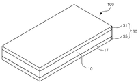
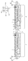
FIG. 1A is a perspective view schematically showing an electronic device module according to an embodiment of the present invention. FIG.
FIG. 1B is a bottom perspective view of the electronic device module shown in FIG. 1A; FIG.
2 is a cross-sectional view of the electronic device module shown in Fig.
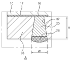
3 is a partially enlarged cross-sectional view showing an enlarged view of a portion A in Fig.
4 is a plan view of the substrate shown in Fig.
5A to 5J are views for explaining a manufacturing method of the electronic device module shown in FIG. 1A;
5K to 5N are views for explaining a method of manufacturing an electronic device module according to another embodiment of the present invention.
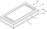
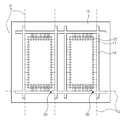
6A is a perspective view schematically showing an electronic device module according to another embodiment of the present invention.
FIG. 6B is a bottom perspective view of the electronic device module shown in FIG. 6A. FIG.
7 is a cross-sectional view of the electronic device module shown in Fig.
8 is a partially enlarged cross-sectional view showing an enlarged view of a portion A in Fig.
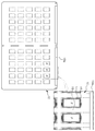
9 is a plan view of the substrate shown in Fig.
10A to 10J are views for explaining a manufacturing method of the electronic element module shown in Fig. 6A. Fig.
11 is a bottom perspective view schematically showing an electronic device module according to another embodiment of the present invention.
Hereinafter, preferred embodiments of the present invention will be described with reference to the accompanying drawings. However, the embodiments of the present invention can be modified into various other forms, and the scope of the present invention is not limited to the embodiments described below. Further, the embodiments of the present invention are provided to more fully explain the present invention to those skilled in the art. In addition, the shape and size of elements in the figures may be exaggerated for clarity.
FIG. 1A is a perspective view schematically showing an electronic device module according to an embodiment of the present invention, and FIG. 1B is a bottom perspective view of the electronic device module shown in FIG. 1A. FIG. 2 is a cross-sectional view of the electronic device module shown in FIG. 1A, FIG. 3 is a partially enlarged cross-sectional view showing an enlarged portion A of FIG. 2, and FIG. 4 is a plan view of the substrate shown in FIG. Here, FIG. 4 shows a state in which electronic elements are mounted, and FIG. 2 shows a cross section corresponding to CC in FIG.
1A to 4, an
The
The
The
A plurality of
The
On the other hand, a
The
The
The
The
The
The
The
The
The connecting
The
The connecting
Therefore, when the
In this case, since a different dissimilar metal such as nickel (Ni) or gold (Au) is not interposed between the
The
The
The other end of the connecting
However, the present invention is not limited to this. The other end of the
In this embodiment, the case where the connecting
Such a
More specifically, the via
For example, the height H of the via-
On the other hand, when the height (length) of the connecting
However, the present invention is not limited to this. When the connecting
The connecting
To this end, the connecting
In the
Accordingly, a plurality of
3 and 4, the
Next, a method of manufacturing an electronic device module according to this embodiment will be described.
5A to 5J are cross-sectional views illustrating a method of manufacturing the electronic device module shown in FIG. 1A.
First, the step of preparing the
Further, the
The
This
in this case. The
The
Then, a step of mounting the
However, the present invention is not limited to this configuration. The
In this step, the same
Subsequently, a step of forming the
In this step, after the
5D, the
Then, as shown in Fig. 5E, the step of mounting the
Next, a step of forming a
Then, a via
The
In the meantime, the via
As described above, the via
More specifically, the via
Therefore, when the mounting height of the
The depth of the via
For example, the via
Subsequently, a connecting
More specifically, as shown in FIG. 5I, the
In FIG. 5I, the
The plating process according to the present embodiment grows a conductive material from the external full-
As described above, the via
In addition, since the size of the via
Therefore, the manufacturing method according to the present embodiment forms the
Also, as described above, the
Therefore, the manufacturing method according to the present embodiment uses a mechanical interlocking (hooking, anchoring theory) or an anchoring effect to plate the conductor on the EMC surface. This means that the adhesive penetrates into the irregular structure (irregularity) of the surface of the adherend and is bonded by mechanical engagement.
That is, in the manufacturing method according to the present embodiment, the inner surface (37a of eh 5h) of the via
For this, in the present embodiment, the inner surface roughness (or roughness) of the via
Even if the molded
On the other hand, in order to increase the bonding force between the
In addition, the surface of the
Finally, a step of cutting the
This step may be performed by cutting the
As a result, the
On the other hand, in the operation of the electronic device module, the plating lines 17 are unnecessary, but these
Although not shown, a step of forming an external terminal (28 in Fig. 3) may be performed at the end of the connecting
Through the above process, the
Meanwhile, the method of manufacturing an electronic device module according to the present invention is not limited to the above-described embodiments, and various modifications are possible.
5K to 5N are views for explaining a method of manufacturing an electronic device module according to another embodiment of the present invention.
First, referring to FIG. 5K, a method for manufacturing an electronic device module according to the present embodiment prepares a
The
In addition, a
Therefore, the
In addition, the
Then, as shown in FIG. 51, an electronic element is mounted on the
The
In this embodiment, the
Then, a via hole is formed in the
Meanwhile, in this step, the electroplating may be performed by electrically connecting the
The current applied to the
Finally, the
This step may be performed by cutting the
Thus, the
The
Further, the
The present invention is not limited to the above-described embodiments, and various modifications are possible.
The embodiments described below are configured similarly to the above embodiment, and have a difference in the configuration of the mold part or the plating line. Therefore, detailed description of the same or similar components to those of the above-described embodiment will be omitted, and differences will be mainly described.
FIG. 6A is a perspective view schematically showing an electronic device module according to another embodiment of the present invention, and FIG. 6B is a bottom perspective view of the electronic device module shown in FIG. 6A. 7 is a cross-sectional view of the electronic device module shown in FIG. 6A, FIG. 8 is a partially enlarged cross-sectional view of the portion A of FIG. 7, and FIG. 9 is a plan view of the substrate shown in FIG. Here, FIG. 9 shows a state in which electronic elements are mounted for convenience of explanation, and FIG. 8 shows a cross section corresponding to CC in FIG.
6A to 9, an
The
The
In the
The
The
The
When the
The
Such a configuration can be realized by a manufacturing method according to an embodiment of the present invention, which will be described later.
The
The
The
The
Also, the
The
The
The connecting
In the
Since the
Next, a method of manufacturing the electronic element module according to the present embodiment will be described.
10A to 10J are cross-sectional views illustrating a method of manufacturing the electronic device module shown in FIG. 6A.
First, a step of preparing the
Further, the
Meanwhile, the
This
At least one through
The through
Then, a step of mounting the
The
In this step, the same
Subsequently, a step of forming a part of the
In this step, the
Meanwhile, the
The
In addition, the
Then, as shown in Fig. 10E, a via
The
Subsequently, the
When the connecting
More specifically, as shown in Fig. 10F, the
The plating process proceeds from the external full-
Then, a step of mounting the
Next, a step of forming the
The molding resin injected into the mold flows into the lower surface B of the
Therefore, the molding resin is formed by forming the
In this process, the further formed
Finally, a step of cutting the
This step may be performed by cutting the
At this time, the cutting line Q is defined such that the
Accordingly, the electronic device module can be separated from the
Although not shown, a step of forming an external connection terminal (28 in Fig. 3) may be performed at the end of the
Through the above process, the
On the other hand, when the problem caused by the plating line exposed to the outside is negligibly small, the outer mold portion may be omitted so that a part of the plating line is exposed to the outside. In this case, the mold part may include only the inner mold part, or may include only the inner mold part and the first mold part.
11 is a bottom perspective view schematically showing an electronic device module according to another embodiment of the present invention.
Referring to FIG. 11, the
The
As described above, the electronic device module according to the present embodiment can be modified into various forms.
While the present invention has been particularly shown and described with reference to exemplary embodiments thereof, it is to be understood that the invention is not limited to the disclosed exemplary embodiments, but, on the contrary, It will be obvious to those of ordinary skill in the art.
100, 200, 300, 400: electronic device module
1: Electronic device
10: substrate
16: Electrode for external connection
17: Plating line
18: pattern for plating
20: connection conductor
28: External terminal
30: Mold part
31: first mold part
35: second mold part
37: via hole
Claims (35)
At least one electronic device mounted thereon;
A mold part sealing the electronic device; And
A plurality of connection conductors extending from the external connection electrode and disposed in the mold part in such a manner as to penetrate the mold part;
.
Electronic device formed by EMC (Epoxy Molding Compound) module.
Wherein the maximum width of the connecting conductor is 1 to 2 times the maximum width of the connecting conductor.
An electronic device module having a height of 200 m or more.
Wherein the mold part is joined to the mold part through a mechanical interlocking mechanism.
Wherein the electronic device module is formed on both sides of the substrate.
And an external terminal connected to an end of the connecting conductor.
Mounting at least one element on the substrate;
Sealing the device to form a mold part;
Forming a via hole in the mold part; And
Forming a connection conductor in the via hole by a plating method through the plating line;
≪ / RTI >
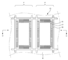
A substrate strip on which a plurality of individual module mounting areas are formed,
Wherein at least one external connection terminal is formed in the individual module mounting area, a conductive pattern is formed outside the individual module mounting area, and the plating line is electrically connected to the external connection terminal Method of manufacturing device module.
Further comprising cutting the substrate strip for each individual module mounting area, wherein the conductive pattern is removed in the cutting step.
And an end of the substrate strip is exposed to the outside of the mold part through a cut surface of the substrate strip.
And the width of the via hole is 1 to 2 times the maximum width of the via hole.
Wherein the height of the electronic device module is 200 mu m or more.
And increasing the roughness of the inner surface of the via hole by using a laser.
And forming the connection conductor by an electrolytic plating process without an electroless plating process.
Wherein the substrate includes an electrode for external connection electrically connected to the plating line,
And forming the via hole includes exposing the external connection electrode to the outside via the via hole.
And a current is applied to the electrode for external connection through the plating line to grow the connection conductor from the electrode for external connection to fill the inside of the via hole.
And bonding the connecting conductor to an inner surface of the via hole through a mechanical interlocking mechanism.
Forming the mold part by using an epoxy molding compound (EMC), and the step of forming the connection conductor is a step of forming the connection conductor through electrolytic copper plating.
And forming an external terminal on the connecting conductor.
And forming an inner mold part so that at least a part of the plating wire is exposed to the outside.
Contacting the metal frame with a plating line exposed to the outside of the inner mold part, and then applying a current to form the connection conductor.
And forming an outer mold part on the outer side of the inner mold part to embed the plating line in the outer mold part.
Wherein a molding resin flows into one surface of the substrate and is formed in a process of forming a new mold part on the other surface of the substrate.
Wherein at least one through hole is formed between the individual module mounting areas and the molding resin flows into one surface of the substrate through the through hole, .
Mounting at least one element on one surface of the substrate;
Forming an inner mold part to seal the element and expose a part of the plating line to the outside;
Forming a via hole in the inner mold part;
Forming a connection conductor in the via hole by a plating method through the plating line; And
Forming an outer mold part on one side of the substrate such that the plating line is completely embedded;
≪ / RTI >
Mounting at least one element on the other surface of the substrate; And
Forming a first mold part by injecting molding resin on the other surface of the substrate;
/ RTI >
Wherein the outer mold part is formed by flowing the molding resin into one surface of the substrate.
At least one electronic device mounted on one surface of the substrate;
An inner mold part sealing the element such that a part of the plating line is exposed to the outside; And
A plurality of connecting conductors extending from the electrode for external connection and disposed in the inner mold part through the inner mold part;
.
And an outer mold part for filling the plating line exposed to the outside of the inner mold part.
An electronic device module formed of different materials.
An electronic device module formed of the same material.
And a first mold part formed on the other surface of the substrate.
An electronic device module formed of the same material.
Priority Applications (2)
| Application Number | Priority Date | Filing Date | Title |
|---|---|---|---|
| US14/724,740 US20160021737A1 (en) | 2014-07-17 | 2015-05-28 | Electric device module and method of manufacturing the same |
| CN201510424692.7A CN105280624A (en) | 2014-07-17 | 2015-07-17 | Electric device module and method of manufacturing the same |
Applications Claiming Priority (2)
| Application Number | Priority Date | Filing Date | Title |
|---|---|---|---|
| KR1020140090550 | 2014-07-17 | ||
| KR20140090550 | 2014-07-17 |
Publications (1)
| Publication Number | Publication Date |
|---|---|
| KR20160010246A true KR20160010246A (en) | 2016-01-27 |
Family
ID=55309530
Family Applications (1)
| Application Number | Title | Priority Date | Filing Date |
|---|---|---|---|
| KR1020140119231A KR20160010246A (en) | 2014-07-17 | 2014-09-05 | Electric component module and manufacturing method threrof |
Country Status (1)
| Country | Link |
|---|---|
| KR (1) | KR20160010246A (en) |
Cited By (2)
| Publication number | Priority date | Publication date | Assignee | Title |
|---|---|---|---|---|
| US10879160B2 (en) | 2018-02-01 | 2020-12-29 | SK Hynix Inc. | Semiconductor package with packaging substrate |
| US10950512B2 (en) | 2018-02-01 | 2021-03-16 | SK Hynix Inc. | Semiconductor packages including a semiconductor chip and methods of forming the semiconductor packages |
Citations (1)
| Publication number | Priority date | Publication date | Assignee | Title |
|---|---|---|---|---|
| JP4840508B2 (en) | 2007-07-06 | 2011-12-21 | 株式会社村田製作所 | Manufacturing method of resin substrate and component built-in substrate, and resin substrate and component built-in substrate |
-
2014
- 2014-09-05 KR KR1020140119231A patent/KR20160010246A/en not_active Application Discontinuation
Patent Citations (1)
| Publication number | Priority date | Publication date | Assignee | Title |
|---|---|---|---|---|
| JP4840508B2 (en) | 2007-07-06 | 2011-12-21 | 株式会社村田製作所 | Manufacturing method of resin substrate and component built-in substrate, and resin substrate and component built-in substrate |
Cited By (3)
| Publication number | Priority date | Publication date | Assignee | Title |
|---|---|---|---|---|
| US10879160B2 (en) | 2018-02-01 | 2020-12-29 | SK Hynix Inc. | Semiconductor package with packaging substrate |
| US10950512B2 (en) | 2018-02-01 | 2021-03-16 | SK Hynix Inc. | Semiconductor packages including a semiconductor chip and methods of forming the semiconductor packages |
| US11557523B2 (en) | 2018-02-01 | 2023-01-17 | SK Hynix Inc. | Semiconductor packages and methods of forming the semiconductor packages |
Similar Documents
| Publication | Publication Date | Title |
|---|---|---|
| US20220102166A1 (en) | Leadframe package with pre-applied filler material | |
| EP2798675B1 (en) | Method for a substrate core layer | |
| US20150062854A1 (en) | Electronic component module and method of manufacturing the same | |
| US20150131231A1 (en) | Electronic component module and manufacturing method thereof | |
| US10573583B2 (en) | Semiconductor device package with grooved substrate | |
| US9510461B2 (en) | Electric component module and method of manufacturing the same | |
| US20160021737A1 (en) | Electric device module and method of manufacturing the same | |
| JP2013236039A (en) | Semiconductor device | |
| KR20180101832A (en) | Electric component module and manufacturing method thereof | |
| US8872329B1 (en) | Extended landing pad substrate package structure and method | |
| US10667419B2 (en) | Manufacturing method of an electronic component module | |
| US10356911B2 (en) | Electronic device module and method of manufacturing the same | |
| KR102117477B1 (en) | Semiconductor package and manufacturing method thereof | |
| KR20160010246A (en) | Electric component module and manufacturing method threrof | |
| KR20150065029A (en) | Printed circuit board, manufacturing method thereof and semiconductor package | |
| KR101983168B1 (en) | Electric component module and manufacturing method threrof | |
| KR20160138754A (en) | Printed circuit board, semiconductor package and method of manufacturing the same | |
| CN107305849B (en) | Packaging structure and manufacturing method thereof | |
| KR20170124769A (en) | Electric component module and manufacturing method threrof | |
| JP6210533B2 (en) | Printed circuit board and manufacturing method thereof | |
| KR101548801B1 (en) | Electric component module and manufacturing method threrof | |
| KR102205195B1 (en) | Semiconductor package with stacked chips and method for fabricating the same | |
| KR101922873B1 (en) | Manufacturing method of electronic component modul | |
| KR101681400B1 (en) | Electronic component module and manufacturing method threrof | |
| KR20160059755A (en) | Electric component module and manufacturing method threrof |
Legal Events
| Date | Code | Title | Description |
|---|---|---|---|
| A201 | Request for examination | ||
| E902 | Notification of reason for refusal |