KR20150136091A - Magnesium alumosilicate-based phosphor - Google Patents
Magnesium alumosilicate-based phosphor Download PDFInfo
- Publication number
- KR20150136091A KR20150136091A KR1020157030383A KR20157030383A KR20150136091A KR 20150136091 A KR20150136091 A KR 20150136091A KR 1020157030383 A KR1020157030383 A KR 1020157030383A KR 20157030383 A KR20157030383 A KR 20157030383A KR 20150136091 A KR20150136091 A KR 20150136091A
- Authority
- KR
- South Korea
- Prior art keywords
- phosphor
- light
- phosphors
- sio
- mixture
- Prior art date
Links
- OAICVXFJPJFONN-UHFFFAOYSA-N Phosphorus Chemical compound [P] OAICVXFJPJFONN-UHFFFAOYSA-N 0.000 title claims description 100
- 229910052749 magnesium Inorganic materials 0.000 title claims description 12
- 239000011777 magnesium Substances 0.000 title description 48
- FYYHWMGAXLPEAU-UHFFFAOYSA-N Magnesium Chemical compound [Mg] FYYHWMGAXLPEAU-UHFFFAOYSA-N 0.000 title 1
- 238000000034 method Methods 0.000 claims abstract description 37
- 150000001875 compounds Chemical class 0.000 claims description 45
- 239000000203 mixture Substances 0.000 claims description 35
- 230000005855 radiation Effects 0.000 claims description 32
- 239000000463 material Substances 0.000 claims description 27
- 239000012298 atmosphere Substances 0.000 claims description 26
- 229910004298 SiO 2 Inorganic materials 0.000 claims description 17
- 238000006243 chemical reaction Methods 0.000 claims description 17
- 229910052710 silicon Inorganic materials 0.000 claims description 14
- 239000002904 solvent Substances 0.000 claims description 14
- 229910052782 aluminium Inorganic materials 0.000 claims description 13
- XUIMIQQOPSSXEZ-UHFFFAOYSA-N Silicon Chemical compound [Si] XUIMIQQOPSSXEZ-UHFFFAOYSA-N 0.000 claims description 12
- 230000008569 process Effects 0.000 claims description 12
- 239000010703 silicon Substances 0.000 claims description 12
- 150000003839 salts Chemical class 0.000 claims description 10
- 238000002360 preparation method Methods 0.000 claims description 8
- 230000001590 oxidative effect Effects 0.000 claims description 7
- 229910052712 strontium Inorganic materials 0.000 claims description 7
- 229910052791 calcium Inorganic materials 0.000 claims description 6
- 238000010438 heat treatment Methods 0.000 claims description 6
- 238000002156 mixing Methods 0.000 claims description 5
- UIIMBOGNXHQVGW-UHFFFAOYSA-M Sodium bicarbonate Chemical group [Na+].OC([O-])=O UIIMBOGNXHQVGW-UHFFFAOYSA-M 0.000 claims description 4
- 229910052738 indium Inorganic materials 0.000 claims description 4
- 229910002601 GaN Inorganic materials 0.000 claims description 3
- 150000002823 nitrates Chemical class 0.000 claims description 3
- ATRRKUHOCOJYRX-UHFFFAOYSA-N Ammonium bicarbonate Chemical compound [NH4+].OC([O-])=O ATRRKUHOCOJYRX-UHFFFAOYSA-N 0.000 claims description 2
- 229910000013 Ammonium bicarbonate Inorganic materials 0.000 claims description 2
- JMASRVWKEDWRBT-UHFFFAOYSA-N Gallium nitride Chemical compound [Ga]#N JMASRVWKEDWRBT-UHFFFAOYSA-N 0.000 claims description 2
- 229910052784 alkaline earth metal Inorganic materials 0.000 claims description 2
- 150000001342 alkaline earth metals Chemical class 0.000 claims description 2
- AUCDRFABNLOFRE-UHFFFAOYSA-N alumane;indium Chemical compound [AlH3].[In] AUCDRFABNLOFRE-UHFFFAOYSA-N 0.000 claims description 2
- 235000012538 ammonium bicarbonate Nutrition 0.000 claims description 2
- 239000001099 ammonium carbonate Substances 0.000 claims description 2
- 229910052799 carbon Inorganic materials 0.000 claims description 2
- 150000004649 carbonic acid derivatives Chemical class 0.000 claims description 2
- 229910052733 gallium Inorganic materials 0.000 claims description 2
- 229910052736 halogen Inorganic materials 0.000 claims description 2
- 150000002367 halogens Chemical class 0.000 claims description 2
- 239000002243 precursor Substances 0.000 claims description 2
- 229910000030 sodium bicarbonate Inorganic materials 0.000 claims description 2
- 235000017557 sodium bicarbonate Nutrition 0.000 claims description 2
- VSCWAEJMTAWNJL-UHFFFAOYSA-K aluminium trichloride Chemical compound Cl[Al](Cl)Cl VSCWAEJMTAWNJL-UHFFFAOYSA-K 0.000 claims 2
- 150000003467 sulfuric acid derivatives Chemical class 0.000 claims 1
- HZVVJJIYJKGMFL-UHFFFAOYSA-N almasilate Chemical class O.[Mg+2].[Al+3].[Al+3].O[Si](O)=O.O[Si](O)=O HZVVJJIYJKGMFL-UHFFFAOYSA-N 0.000 abstract description 3
- 230000005693 optoelectronics Effects 0.000 abstract description 2
- 238000000576 coating method Methods 0.000 description 17
- 239000011248 coating agent Substances 0.000 description 16
- 229910004283 SiO 4 Inorganic materials 0.000 description 14
- XLYOFNOQVPJJNP-UHFFFAOYSA-N water Substances O XLYOFNOQVPJJNP-UHFFFAOYSA-N 0.000 description 13
- 239000011734 sodium Substances 0.000 description 12
- 239000010410 layer Substances 0.000 description 10
- 229910052725 zinc Inorganic materials 0.000 description 10
- 238000005286 illumination Methods 0.000 description 9
- 239000002245 particle Substances 0.000 description 9
- 239000000919 ceramic Substances 0.000 description 8
- 239000008367 deionised water Substances 0.000 description 8
- 229910021641 deionized water Inorganic materials 0.000 description 8
- 229920005989 resin Polymers 0.000 description 8
- 239000011347 resin Substances 0.000 description 8
- 239000000243 solution Substances 0.000 description 8
- 229910017639 MgSi Inorganic materials 0.000 description 7
- 230000000875 corresponding effect Effects 0.000 description 7
- 238000000295 emission spectrum Methods 0.000 description 7
- 230000005284 excitation Effects 0.000 description 7
- 229910052709 silver Inorganic materials 0.000 description 7
- 229910004261 CaF 2 Inorganic materials 0.000 description 6
- 229910004762 CaSiO Inorganic materials 0.000 description 6
- 229910052688 Gadolinium Inorganic materials 0.000 description 6
- 229910003668 SrAl Inorganic materials 0.000 description 6
- 238000009877 rendering Methods 0.000 description 6
- 229910052950 sphalerite Inorganic materials 0.000 description 6
- 239000000126 substance Substances 0.000 description 6
- 229910052984 zinc sulfide Inorganic materials 0.000 description 6
- 101100476480 Mus musculus S100a8 gene Proteins 0.000 description 5
- QVGXLLKOCUKJST-UHFFFAOYSA-N atomic oxygen Chemical compound [O] QVGXLLKOCUKJST-UHFFFAOYSA-N 0.000 description 5
- 229910052788 barium Inorganic materials 0.000 description 5
- 238000000975 co-precipitation Methods 0.000 description 5
- 238000004519 manufacturing process Methods 0.000 description 5
- 229910052751 metal Inorganic materials 0.000 description 5
- 239000002184 metal Substances 0.000 description 5
- 229910052760 oxygen Inorganic materials 0.000 description 5
- 239000001301 oxygen Substances 0.000 description 5
- 238000003825 pressing Methods 0.000 description 5
- 238000010791 quenching Methods 0.000 description 5
- 238000000177 wavelength dispersive X-ray spectroscopy Methods 0.000 description 5
- 229910018072 Al 2 O 3 Inorganic materials 0.000 description 4
- NLXLAEXVIDQMFP-UHFFFAOYSA-N Ammonia chloride Chemical compound [NH4+].[Cl-] NLXLAEXVIDQMFP-UHFFFAOYSA-N 0.000 description 4
- 229910052684 Cerium Inorganic materials 0.000 description 4
- 229910010413 TiO 2 Inorganic materials 0.000 description 4
- 229910052801 chlorine Inorganic materials 0.000 description 4
- 229910052802 copper Inorganic materials 0.000 description 4
- 238000005516 engineering process Methods 0.000 description 4
- 229910052748 manganese Inorganic materials 0.000 description 4
- 230000000171 quenching effect Effects 0.000 description 4
- 230000035945 sensitivity Effects 0.000 description 4
- 230000003595 spectral effect Effects 0.000 description 4
- 229910052718 tin Inorganic materials 0.000 description 4
- 229910052727 yttrium Inorganic materials 0.000 description 4
- 229910052693 Europium Inorganic materials 0.000 description 3
- 229910021193 La 2 O 3 Inorganic materials 0.000 description 3
- OKKJLVBELUTLKV-UHFFFAOYSA-N Methanol Chemical compound OC OKKJLVBELUTLKV-UHFFFAOYSA-N 0.000 description 3
- BPQQTUXANYXVAA-UHFFFAOYSA-N Orthosilicate Chemical compound [O-][Si]([O-])([O-])[O-] BPQQTUXANYXVAA-UHFFFAOYSA-N 0.000 description 3
- 229910052771 Terbium Inorganic materials 0.000 description 3
- 229910008484 TiSi Inorganic materials 0.000 description 3
- 238000002441 X-ray diffraction Methods 0.000 description 3
- GEIAQOFPUVMAGM-UHFFFAOYSA-N ZrO Inorganic materials [Zr]=O GEIAQOFPUVMAGM-UHFFFAOYSA-N 0.000 description 3
- 239000012190 activator Substances 0.000 description 3
- 238000000137 annealing Methods 0.000 description 3
- 230000008901 benefit Effects 0.000 description 3
- 239000011230 binding agent Substances 0.000 description 3
- 229910052793 cadmium Inorganic materials 0.000 description 3
- 230000000052 comparative effect Effects 0.000 description 3
- 230000002596 correlated effect Effects 0.000 description 3
- 230000007423 decrease Effects 0.000 description 3
- 230000000694 effects Effects 0.000 description 3
- 230000005670 electromagnetic radiation Effects 0.000 description 3
- 125000000524 functional group Chemical group 0.000 description 3
- 239000011521 glass Substances 0.000 description 3
- -1 halogenides Chemical class 0.000 description 3
- 229920000647 polyepoxide Polymers 0.000 description 3
- 238000000746 purification Methods 0.000 description 3
- 229920002050 silicone resin Polymers 0.000 description 3
- 238000007704 wet chemistry method Methods 0.000 description 3
- QGZKDVFQNNGYKY-UHFFFAOYSA-N Ammonia Chemical compound N QGZKDVFQNNGYKY-UHFFFAOYSA-N 0.000 description 2
- IJGRMHOSHXDMSA-UHFFFAOYSA-N Atomic nitrogen Chemical compound N#N IJGRMHOSHXDMSA-UHFFFAOYSA-N 0.000 description 2
- UGFAIRIUMAVXCW-UHFFFAOYSA-N Carbon monoxide Chemical compound [O+]#[C-] UGFAIRIUMAVXCW-UHFFFAOYSA-N 0.000 description 2
- 239000004593 Epoxy Substances 0.000 description 2
- LFQSCWFLJHTTHZ-UHFFFAOYSA-N Ethanol Chemical compound CCO LFQSCWFLJHTTHZ-UHFFFAOYSA-N 0.000 description 2
- 229910002420 LaOCl Inorganic materials 0.000 description 2
- 229910010199 LiAl Inorganic materials 0.000 description 2
- 229910010093 LiAlO Inorganic materials 0.000 description 2
- 101100496858 Mus musculus Colec12 gene Proteins 0.000 description 2
- 229910003564 SiAlON Inorganic materials 0.000 description 2
- BQCADISMDOOEFD-UHFFFAOYSA-N Silver Chemical compound [Ag] BQCADISMDOOEFD-UHFFFAOYSA-N 0.000 description 2
- 229910002367 SrTiO Inorganic materials 0.000 description 2
- 238000010521 absorption reaction Methods 0.000 description 2
- 235000019270 ammonium chloride Nutrition 0.000 description 2
- 239000007864 aqueous solution Substances 0.000 description 2
- 229910052794 bromium Inorganic materials 0.000 description 2
- 229910002091 carbon monoxide Inorganic materials 0.000 description 2
- 229910052804 chromium Inorganic materials 0.000 description 2
- 238000007796 conventional method Methods 0.000 description 2
- 230000002950 deficient Effects 0.000 description 2
- 238000010586 diagram Methods 0.000 description 2
- 238000009792 diffusion process Methods 0.000 description 2
- 239000006185 dispersion Substances 0.000 description 2
- 238000001704 evaporation Methods 0.000 description 2
- 230000008020 evaporation Effects 0.000 description 2
- 229910052731 fluorine Inorganic materials 0.000 description 2
- 230000004907 flux Effects 0.000 description 2
- 239000002223 garnet Substances 0.000 description 2
- 229910052739 hydrogen Inorganic materials 0.000 description 2
- 239000001257 hydrogen Substances 0.000 description 2
- 125000004435 hydrogen atom Chemical class [H]* 0.000 description 2
- 238000005259 measurement Methods 0.000 description 2
- 238000002844 melting Methods 0.000 description 2
- 230000008018 melting Effects 0.000 description 2
- 239000010445 mica Substances 0.000 description 2
- 229910052618 mica group Inorganic materials 0.000 description 2
- 238000012986 modification Methods 0.000 description 2
- 230000004048 modification Effects 0.000 description 2
- 229910052759 nickel Inorganic materials 0.000 description 2
- 150000004767 nitrides Chemical class 0.000 description 2
- 230000003647 oxidation Effects 0.000 description 2
- 238000007254 oxidation reaction Methods 0.000 description 2
- 229910052698 phosphorus Inorganic materials 0.000 description 2
- 239000000843 powder Substances 0.000 description 2
- 238000001556 precipitation Methods 0.000 description 2
- SBIBMFFZSBJNJF-UHFFFAOYSA-N selenium;zinc Chemical compound [Se]=[Zn] SBIBMFFZSBJNJF-UHFFFAOYSA-N 0.000 description 2
- 239000004065 semiconductor Substances 0.000 description 2
- 239000004332 silver Substances 0.000 description 2
- SQGYOTSLMSWVJD-UHFFFAOYSA-N silver(1+) nitrate Chemical compound [Ag+].[O-]N(=O)=O SQGYOTSLMSWVJD-UHFFFAOYSA-N 0.000 description 2
- 239000007787 solid Substances 0.000 description 2
- 239000007858 starting material Substances 0.000 description 2
- XLOMVQKBTHCTTD-UHFFFAOYSA-N zinc oxide Inorganic materials [Zn]=O XLOMVQKBTHCTTD-UHFFFAOYSA-N 0.000 description 2
- 229910015999 BaAl Inorganic materials 0.000 description 1
- 229910016066 BaSi Inorganic materials 0.000 description 1
- 101150027751 Casr gene Proteins 0.000 description 1
- VEXZGXHMUGYJMC-UHFFFAOYSA-M Chloride anion Chemical compound [Cl-] VEXZGXHMUGYJMC-UHFFFAOYSA-M 0.000 description 1
- WQZGKKKJIJFFOK-GASJEMHNSA-N Glucose Natural products OC[C@H]1OC(O)[C@H](O)[C@@H](O)[C@@H]1O WQZGKKKJIJFFOK-GASJEMHNSA-N 0.000 description 1
- 229910017414 LaAl Inorganic materials 0.000 description 1
- 229910012506 LiSi Inorganic materials 0.000 description 1
- 229910052765 Lutetium Inorganic materials 0.000 description 1
- 229910020068 MgAl Inorganic materials 0.000 description 1
- 229910017857 MgGa Inorganic materials 0.000 description 1
- 229910017625 MgSiO Inorganic materials 0.000 description 1
- BKQMNPVDJIHLPD-UHFFFAOYSA-N OS(=O)(=O)[Se]S(O)(=O)=O Chemical compound OS(=O)(=O)[Se]S(O)(=O)=O BKQMNPVDJIHLPD-UHFFFAOYSA-N 0.000 description 1
- 229910052777 Praseodymium Inorganic materials 0.000 description 1
- QAOWNCQODCNURD-UHFFFAOYSA-N Sulfuric acid Chemical class OS(O)(=O)=O QAOWNCQODCNURD-UHFFFAOYSA-N 0.000 description 1
- BOTDANWDWHJENH-UHFFFAOYSA-N Tetraethyl orthosilicate Chemical compound CCO[Si](OCC)(OCC)OCC BOTDANWDWHJENH-UHFFFAOYSA-N 0.000 description 1
- 238000006887 Ullmann reaction Methods 0.000 description 1
- 229910007709 ZnTe Inorganic materials 0.000 description 1
- 238000000862 absorption spectrum Methods 0.000 description 1
- 150000001298 alcohols Chemical class 0.000 description 1
- 150000004645 aluminates Chemical class 0.000 description 1
- XAGFODPZIPBFFR-UHFFFAOYSA-N aluminium Chemical compound [Al] XAGFODPZIPBFFR-UHFFFAOYSA-N 0.000 description 1
- PNEYBMLMFCGWSK-UHFFFAOYSA-N aluminium oxide Inorganic materials [O-2].[O-2].[O-2].[Al+3].[Al+3] PNEYBMLMFCGWSK-UHFFFAOYSA-N 0.000 description 1
- 229910021529 ammonia Inorganic materials 0.000 description 1
- 229910052787 antimony Inorganic materials 0.000 description 1
- 125000004429 atom Chemical group 0.000 description 1
- 230000009286 beneficial effect Effects 0.000 description 1
- 229910052790 beryllium Inorganic materials 0.000 description 1
- WQZGKKKJIJFFOK-VFUOTHLCSA-N beta-D-glucose Chemical compound OC[C@H]1O[C@@H](O)[C@H](O)[C@@H](O)[C@@H]1O WQZGKKKJIJFFOK-VFUOTHLCSA-N 0.000 description 1
- 238000009835 boiling Methods 0.000 description 1
- 229910052980 cadmium sulfide Inorganic materials 0.000 description 1
- 238000001354 calcination Methods 0.000 description 1
- 238000005266 casting Methods 0.000 description 1
- 230000015556 catabolic process Effects 0.000 description 1
- 229910010293 ceramic material Inorganic materials 0.000 description 1
- 230000008859 change Effects 0.000 description 1
- 239000007795 chemical reaction product Substances 0.000 description 1
- 239000003795 chemical substances by application Substances 0.000 description 1
- 230000006835 compression Effects 0.000 description 1
- 238000007906 compression Methods 0.000 description 1
- 238000002425 crystallisation Methods 0.000 description 1
- 230000008025 crystallization Effects 0.000 description 1
- 230000003247 decreasing effect Effects 0.000 description 1
- 238000006731 degradation reaction Methods 0.000 description 1
- 230000001419 dependent effect Effects 0.000 description 1
- 238000009826 distribution Methods 0.000 description 1
- 239000002019 doping agent Substances 0.000 description 1
- 238000005401 electroluminescence Methods 0.000 description 1
- 238000004049 embossing Methods 0.000 description 1
- 238000005538 encapsulation Methods 0.000 description 1
- 230000007613 environmental effect Effects 0.000 description 1
- 150000002118 epoxides Chemical class 0.000 description 1
- 239000003822 epoxy resin Substances 0.000 description 1
- 150000002148 esters Chemical class 0.000 description 1
- 238000005530 etching Methods 0.000 description 1
- 238000000695 excitation spectrum Methods 0.000 description 1
- 238000002474 experimental method Methods 0.000 description 1
- 230000002349 favourable effect Effects 0.000 description 1
- 239000007789 gas Substances 0.000 description 1
- 230000008570 general process Effects 0.000 description 1
- 229910052732 germanium Inorganic materials 0.000 description 1
- 239000008103 glucose Substances 0.000 description 1
- 229910052737 gold Inorganic materials 0.000 description 1
- 238000000227 grinding Methods 0.000 description 1
- 230000006872 improvement Effects 0.000 description 1
- 238000010348 incorporation Methods 0.000 description 1
- 229910021331 inorganic silicon compound Inorganic materials 0.000 description 1
- 229910052740 iodine Inorganic materials 0.000 description 1
- 150000002500 ions Chemical class 0.000 description 1
- 229910052746 lanthanum Inorganic materials 0.000 description 1
- 229910052745 lead Inorganic materials 0.000 description 1
- 239000004973 liquid crystal related substance Substances 0.000 description 1
- 238000004020 luminiscence type Methods 0.000 description 1
- OHSVLFRHMCKCQY-UHFFFAOYSA-N lutetium atom Chemical compound [Lu] OHSVLFRHMCKCQY-UHFFFAOYSA-N 0.000 description 1
- QSHDDOUJBYECFT-UHFFFAOYSA-N mercury Chemical compound [Hg] QSHDDOUJBYECFT-UHFFFAOYSA-N 0.000 description 1
- 229910052753 mercury Inorganic materials 0.000 description 1
- 238000001465 metallisation Methods 0.000 description 1
- 239000011259 mixed solution Substances 0.000 description 1
- 229910052757 nitrogen Inorganic materials 0.000 description 1
- 229910000510 noble metal Inorganic materials 0.000 description 1
- 230000003287 optical effect Effects 0.000 description 1
- 150000002894 organic compounds Chemical class 0.000 description 1
- 150000003961 organosilicon compounds Chemical class 0.000 description 1
- 125000004043 oxo group Chemical group O=* 0.000 description 1
- 238000005424 photoluminescence Methods 0.000 description 1
- 239000004038 photonic crystal Substances 0.000 description 1
- 229920006254 polymer film Polymers 0.000 description 1
- 235000019353 potassium silicate Nutrition 0.000 description 1
- 238000010248 power generation Methods 0.000 description 1
- 239000000047 product Substances 0.000 description 1
- 230000001902 propagating effect Effects 0.000 description 1
- 238000006862 quantum yield reaction Methods 0.000 description 1
- 229910052761 rare earth metal Inorganic materials 0.000 description 1
- 230000009467 reduction Effects 0.000 description 1
- 230000027756 respiratory electron transport chain Effects 0.000 description 1
- 230000004044 response Effects 0.000 description 1
- 150000004760 silicates Chemical class 0.000 description 1
- 229910001961 silver nitrate Inorganic materials 0.000 description 1
- 239000002356 single layer Substances 0.000 description 1
- 239000002002 slurry Substances 0.000 description 1
- 239000005361 soda-lime glass Substances 0.000 description 1
- 229910052708 sodium Inorganic materials 0.000 description 1
- NTHWMYGWWRZVTN-UHFFFAOYSA-N sodium silicate Chemical compound [Na+].[Na+].[O-][Si]([O-])=O NTHWMYGWWRZVTN-UHFFFAOYSA-N 0.000 description 1
- 239000007790 solid phase Substances 0.000 description 1
- 238000001228 spectrum Methods 0.000 description 1
- 239000012798 spherical particle Substances 0.000 description 1
- 239000000725 suspension Substances 0.000 description 1
- 229910052714 tellurium Inorganic materials 0.000 description 1
- LFQCEHFDDXELDD-UHFFFAOYSA-N tetramethyl orthosilicate Chemical compound CO[Si](OC)(OC)OC LFQCEHFDDXELDD-UHFFFAOYSA-N 0.000 description 1
- 229910052716 thallium Inorganic materials 0.000 description 1
- 238000012546 transfer Methods 0.000 description 1
- 229910052721 tungsten Inorganic materials 0.000 description 1
- 238000002211 ultraviolet spectrum Methods 0.000 description 1
- 238000009827 uniform distribution Methods 0.000 description 1
- LSGOVYNHVSXFFJ-UHFFFAOYSA-N vanadate(3-) Chemical class [O-][V]([O-])([O-])=O LSGOVYNHVSXFFJ-UHFFFAOYSA-N 0.000 description 1
- 229910052720 vanadium Inorganic materials 0.000 description 1
- 229910052724 xenon Inorganic materials 0.000 description 1
- FHNFHKCVQCLJFQ-UHFFFAOYSA-N xenon atom Chemical compound [Xe] FHNFHKCVQCLJFQ-UHFFFAOYSA-N 0.000 description 1
Images


Classifications
-
- C—CHEMISTRY; METALLURGY
- C09—DYES; PAINTS; POLISHES; NATURAL RESINS; ADHESIVES; COMPOSITIONS NOT OTHERWISE PROVIDED FOR; APPLICATIONS OF MATERIALS NOT OTHERWISE PROVIDED FOR
- C09K—MATERIALS FOR MISCELLANEOUS APPLICATIONS, NOT PROVIDED FOR ELSEWHERE
- C09K11/00—Luminescent, e.g. electroluminescent, chemiluminescent materials
- C09K11/08—Luminescent, e.g. electroluminescent, chemiluminescent materials containing inorganic luminescent materials
- C09K11/77—Luminescent, e.g. electroluminescent, chemiluminescent materials containing inorganic luminescent materials containing rare earth metals
- C09K11/7728—Luminescent, e.g. electroluminescent, chemiluminescent materials containing inorganic luminescent materials containing rare earth metals containing europium
- C09K11/7734—Aluminates
-
- C—CHEMISTRY; METALLURGY
- C09—DYES; PAINTS; POLISHES; NATURAL RESINS; ADHESIVES; COMPOSITIONS NOT OTHERWISE PROVIDED FOR; APPLICATIONS OF MATERIALS NOT OTHERWISE PROVIDED FOR
- C09K—MATERIALS FOR MISCELLANEOUS APPLICATIONS, NOT PROVIDED FOR ELSEWHERE
- C09K11/00—Luminescent, e.g. electroluminescent, chemiluminescent materials
- C09K11/08—Luminescent, e.g. electroluminescent, chemiluminescent materials containing inorganic luminescent materials
- C09K11/77—Luminescent, e.g. electroluminescent, chemiluminescent materials containing inorganic luminescent materials containing rare earth metals
- C09K11/7728—Luminescent, e.g. electroluminescent, chemiluminescent materials containing inorganic luminescent materials containing rare earth metals containing europium
- C09K11/77344—Aluminosilicates
-
- F—MECHANICAL ENGINEERING; LIGHTING; HEATING; WEAPONS; BLASTING
- F21—LIGHTING
- F21K—NON-ELECTRIC LIGHT SOURCES USING LUMINESCENCE; LIGHT SOURCES USING ELECTROCHEMILUMINESCENCE; LIGHT SOURCES USING CHARGES OF COMBUSTIBLE MATERIAL; LIGHT SOURCES USING SEMICONDUCTOR DEVICES AS LIGHT-GENERATING ELEMENTS; LIGHT SOURCES NOT OTHERWISE PROVIDED FOR
- F21K9/00—Light sources using semiconductor devices as light-generating elements, e.g. using light-emitting diodes [LED] or lasers
- F21K9/60—Optical arrangements integrated in the light source, e.g. for improving the colour rendering index or the light extraction
- F21K9/64—Optical arrangements integrated in the light source, e.g. for improving the colour rendering index or the light extraction using wavelength conversion means distinct or spaced from the light-generating element, e.g. a remote phosphor layer
-
- G—PHYSICS
- G02—OPTICS
- G02B—OPTICAL ELEMENTS, SYSTEMS OR APPARATUS
- G02B5/00—Optical elements other than lenses
- G02B5/20—Filters
- G02B5/208—Filters for use with infrared or ultraviolet radiation, e.g. for separating visible light from infrared and/or ultraviolet radiation
-
- H—ELECTRICITY
- H01—ELECTRIC ELEMENTS
- H01J—ELECTRIC DISCHARGE TUBES OR DISCHARGE LAMPS
- H01J1/00—Details of electrodes, of magnetic control means, of screens, or of the mounting or spacing thereof, common to two or more basic types of discharge tubes or lamps
- H01J1/54—Screens on or from which an image or pattern is formed, picked-up, converted, or stored; Luminescent coatings on vessels
- H01J1/62—Luminescent screens; Selection of materials for luminescent coatings on vessels
- H01J1/63—Luminescent screens; Selection of materials for luminescent coatings on vessels characterised by the luminescent material
-
- H—ELECTRICITY
- H01—ELECTRIC ELEMENTS
- H01J—ELECTRIC DISCHARGE TUBES OR DISCHARGE LAMPS
- H01J61/00—Gas-discharge or vapour-discharge lamps
- H01J61/02—Details
- H01J61/38—Devices for influencing the colour or wavelength of the light
- H01J61/42—Devices for influencing the colour or wavelength of the light by transforming the wavelength of the light by luminescence
- H01J61/44—Devices characterised by the luminescent material
-
- H—ELECTRICITY
- H01—ELECTRIC ELEMENTS
- H01L—SEMICONDUCTOR DEVICES NOT COVERED BY CLASS H10
- H01L33/00—Semiconductor devices with at least one potential-jump barrier or surface barrier specially adapted for light emission; Processes or apparatus specially adapted for the manufacture or treatment thereof or of parts thereof; Details thereof
- H01L33/02—Semiconductor devices with at least one potential-jump barrier or surface barrier specially adapted for light emission; Processes or apparatus specially adapted for the manufacture or treatment thereof or of parts thereof; Details thereof characterised by the semiconductor bodies
- H01L33/26—Materials of the light emitting region
- H01L33/30—Materials of the light emitting region containing only elements of group III and group V of the periodic system
- H01L33/32—Materials of the light emitting region containing only elements of group III and group V of the periodic system containing nitrogen
-
- H—ELECTRICITY
- H01—ELECTRIC ELEMENTS
- H01L—SEMICONDUCTOR DEVICES NOT COVERED BY CLASS H10
- H01L33/00—Semiconductor devices with at least one potential-jump barrier or surface barrier specially adapted for light emission; Processes or apparatus specially adapted for the manufacture or treatment thereof or of parts thereof; Details thereof
- H01L33/48—Semiconductor devices with at least one potential-jump barrier or surface barrier specially adapted for light emission; Processes or apparatus specially adapted for the manufacture or treatment thereof or of parts thereof; Details thereof characterised by the semiconductor body packages
- H01L33/50—Wavelength conversion elements
- H01L33/501—Wavelength conversion elements characterised by the materials, e.g. binder
- H01L33/502—Wavelength conversion materials
-
- H—ELECTRICITY
- H01—ELECTRIC ELEMENTS
- H01L—SEMICONDUCTOR DEVICES NOT COVERED BY CLASS H10
- H01L31/00—Semiconductor devices sensitive to infrared radiation, light, electromagnetic radiation of shorter wavelength or corpuscular radiation and specially adapted either for the conversion of the energy of such radiation into electrical energy or for the control of electrical energy by such radiation; Processes or apparatus specially adapted for the manufacture or treatment thereof or of parts thereof; Details thereof
- H01L31/02—Details
- H01L31/0232—Optical elements or arrangements associated with the device
- H01L31/02322—Optical elements or arrangements associated with the device comprising luminescent members, e.g. fluorescent sheets upon the device
-
- H—ELECTRICITY
- H01—ELECTRIC ELEMENTS
- H01L—SEMICONDUCTOR DEVICES NOT COVERED BY CLASS H10
- H01L31/00—Semiconductor devices sensitive to infrared radiation, light, electromagnetic radiation of shorter wavelength or corpuscular radiation and specially adapted either for the conversion of the energy of such radiation into electrical energy or for the control of electrical energy by such radiation; Processes or apparatus specially adapted for the manufacture or treatment thereof or of parts thereof; Details thereof
- H01L31/04—Semiconductor devices sensitive to infrared radiation, light, electromagnetic radiation of shorter wavelength or corpuscular radiation and specially adapted either for the conversion of the energy of such radiation into electrical energy or for the control of electrical energy by such radiation; Processes or apparatus specially adapted for the manufacture or treatment thereof or of parts thereof; Details thereof adapted as photovoltaic [PV] conversion devices
- H01L31/054—Optical elements directly associated or integrated with the PV cell, e.g. light-reflecting means or light-concentrating means
- H01L31/055—Optical elements directly associated or integrated with the PV cell, e.g. light-reflecting means or light-concentrating means where light is absorbed and re-emitted at a different wavelength by the optical element directly associated or integrated with the PV cell, e.g. by using luminescent material, fluorescent concentrators or up-conversion arrangements
-
- Y—GENERAL TAGGING OF NEW TECHNOLOGICAL DEVELOPMENTS; GENERAL TAGGING OF CROSS-SECTIONAL TECHNOLOGIES SPANNING OVER SEVERAL SECTIONS OF THE IPC; TECHNICAL SUBJECTS COVERED BY FORMER USPC CROSS-REFERENCE ART COLLECTIONS [XRACs] AND DIGESTS
- Y02—TECHNOLOGIES OR APPLICATIONS FOR MITIGATION OR ADAPTATION AGAINST CLIMATE CHANGE
- Y02E—REDUCTION OF GREENHOUSE GAS [GHG] EMISSIONS, RELATED TO ENERGY GENERATION, TRANSMISSION OR DISTRIBUTION
- Y02E10/00—Energy generation through renewable energy sources
- Y02E10/50—Photovoltaic [PV] energy
- Y02E10/52—PV systems with concentrators
Abstract
본 발명은, 공-활성화된 마그네슘 알루미노실리케이트계 인광체, 상기 인광체의 제조 방법, 전자 및 전광 장치(예컨대 발광 다이오드 (LED) 및 태양 전지)에서의 상기 인광체의 용도, 및 특히 상기 인광체를 포함하는 조명 유닛에 관한 것이다.The present invention relates to the use of such phosphors in co-activated magnesium aluminosilicate phosphors, methods of making the phosphors, electronic and optoelectronic devices such as light emitting diodes (LEDs) and solar cells, To a lighting unit.
Description
본 발명은, 공-활성화된 마그네슘 알루미노실리케이트계 인광체, 상기 인광체의 제조 방법, 전자 및 전광 장치(예컨대 발광 다이오드(LED) 및 태양 전지)에서의 상기 인광체의 용도, 및 특히 상기 인광체를 포함하는 조명 유닛(illumination unit)에 관한 것이다.The present invention relates to the use of such phosphors in co-activated magnesium aluminosilicate phosphors, methods of making the phosphors, electronic and optoelectronic devices such as light emitting diodes (LEDs) and solar cells, To an illumination unit.
백색 발광 다이오드(LED)는 높은 효율, 긴 수명, 적은 환경 영향, 수은의 부재, 짧은 응답 시간, 다양한 크기의 최종 제품에서의 적용 가능성, 및 많은 더 유리한 특성을 보여준다. 이들은, 액정 디스플레이, 노트북 컴퓨터 모니터, 휴대폰 스크린에 대한 후면-조명원으로서, 및 일반적인 조명에서 주목을 받고 있다. White light-emitting diodes (LEDs) show high efficiency, long lifetime, low environmental impact, absence of mercury, short response times, applicability in various sizes of end products, and many more favorable characteristics. They are receiving attention in liquid-crystal displays, notebook computer monitors, back-lighting sources for cell phone screens, and general lighting.
당업계 숙련자에게 공지된 바와 같이, 백색 LED는, 황색 발광 인광체(예컨대, 560 nm 부근의 발광 피크 파장을 나타내는 YAG:Ce)를 청색 발광 LED에 가함으로써 수득될 수 있다. 상응하는 청색 발광 LED의 방출된 피크 파장은 전형적으로 450 내지 470 nm의 범위이다. 따라서, 인광체가 청색 LED로부터 방출된 범위의 광을 흡수해야 하기 때문에, 한정된 개수의 인광체만이 백색 LED를 수득하는데 사용될 수 있다. As is known to those skilled in the art, a white LED can be obtained by adding a yellow light emitting phosphor (for example, YAG: Ce which exhibits an emission peak wavelength around 560 nm) to a blue light emitting LED. The emitted peak wavelength of the corresponding blue emitting LED is typically in the range of 450 to 470 nm. Thus, only a limited number of phosphors can be used to obtain a white LED, since the phosphors must absorb light in the range emitted from the blue LED.
주요 광원으로서, 전형적으로 280 내지 400 nm의 범위의 파장을 갖는 광을 방출하는 근자외선-LED와 적색, 녹색 및 청색 발광 인광체를 조합하여, 전술된 백색 LED에 비해 더 우수한 발광 강도 및 더 뛰어난 백색을 갖는 3-색 백색 LED를 수득할 수 있다. 결과적으로, 280 nm 내지 400 nm 범위의 파장에서 여기될 수 있는 인광체에 대한 상당한 요구가 존재한다. As a primary light source, a near-ultraviolet-LED emitting light having a wavelength in the range of typically 280 to 400 nm and a combination of red, green and blue luminescent phosphors have been found to have superior luminescence intensity and superior A 3-color white LED having a white color can be obtained. As a result, there is a great need for phosphors that can be excited at wavelengths ranging from 280 nm to 400 nm.
자외선-LED 또는 근자외선-LED를 사용하여 이러한 백색 LED를 수득하기 위해, 전형적으로 적색, 녹색, 및 청색 발광 인광체를 먼저 적합한 수지 내에서 혼합한다. 이어서 수득된 겔을 자외선-LED 칩 또는 근자외선-LED 칩 상에 놓고, 자외선 조사, 어닐링, 또는 유사 공정을 사용하여 경화시킨다. 모든 각도에서 칩을 볼 때, 고른 백색 칼라를 관찰하기 위해서는 수지 내의 인광체 혼합물이 가능한한 균일하게 분산되어야 한다. 하지만, 수지 내의 상이한 인광체의 균일한 분포를 수득하는 것은, 이의 상이한 입자 크기, 모양 및/또는 수지 내의 이의 밀도 때문에 어렵다. 따라서, 3종 미만의 인광체 또는 심지어는 단 하나의 인광체 만을 사용하는 것이 유리하다. 예를 들어, 상이한 파장에서 2개 이상의 주 발광 피크를 갖는 인광체를 사용하면 전술된 문제를 해결할 수 있게 된다.To obtain these white LEDs using ultraviolet-LED or near-ultraviolet-LED, typically red, green, and blue emitting phosphors are first mixed in a suitable resin. The resulting gel is then placed on an ultraviolet-LED chip or near-ultraviolet-LED chip and cured using ultraviolet radiation, annealing, or the like process. When viewing the chip at all angles, it is necessary to disperse the phosphor mixture in the resin as uniformly as possible in order to observe the even white color. However, it is difficult to obtain a uniform distribution of the different phosphors in the resin because of its different particle size, shape and / or its density in the resin. Thus, it is advantageous to use less than three phosphors or even only one phosphor. For example, using the phosphor having two or more main emission peaks at different wavelengths can solve the above-described problem.
이와 관련하여, 이성훈(Sung Hun Lee), 박제홍(Je Hong Park), 손세모(Se Mo Son) 및 김종수(Jong Su Kim)는 문헌[Appl. Phys. Lett. 2006, 89, 221916]에서, 440 nm 및 680 nm에서 주요 피크를 갖고 대략 450 nm, 580 nm, 및 680 nm 부근에서 광을 방출하는 3개의 발광 밴드를 나타내는, CaMgSi2O6:Eu2 +,Mn2 + 인광체를 개시한다. 육안 상 가장 바람직한 스펙트럼 범위가 400 내지 650 nm이므로, 680 nm에서의 발광 피크는 가시광선의 가장자리에 위치한다. 또한, 4845 내지 9180 K의 상관 색온도 및 71% 내지 88%의 연색(color rendering) 지수를 갖는 백색 광을 수득하기 위해, 녹색-부족 CaMgSi2O6:Eu2 +,Mn2 + 및 녹색-황색 발광 (Ba,Sr)2SiO4:Eu2 +의 혼합물이 필요하다.In this regard, Sung Hun Lee, Je Hong Park, Se Mo Son, and Jong Su Kim have been described in Appl. Phys. Lett. 2006, 89, 221 916] in, 440 nm and 680 nm has a main peak at approximately 450 nm, representing the three light-emitting band, which emits light at around 580 nm, and 680 nm, CaMgSi 2 O 6: Eu 2 +, Mn 2 + phosphors. Since the most preferable spectral range from the naked eye is 400 to 650 nm, the emission peak at 680 nm is located at the edge of the visible light line. Also, 4845 to 9180 K in the correlated color temperature and color rendering index of 71% to 88% (color rendering) to give a white light having an index, green- lack CaMgSi 2 O 6: Eu 2 + , Mn 2 + and a green-yellow light-emitting (Ba, Sr) 2 SiO 4 : Eu 2 + of the mixture is required.
하지만, 자외선 또는 근자외선-LED를 사용하여 백색 LED를 생산해내기 위해 2개의 인광체의 혼합물을 사용하여도, 수지 내에서 상이한 크기, 입자 모양 및 밀도를 갖는 인광체를 균일하게 혼합하기가 여전히 어렵다. 또한, 인광체가 가시광 범위에 위치된 파장에 의해 여기되어서는 안된다. 예를 들어, 녹색 인광체의 방출 스펙트럼이 적색 인광체의 여기 스펙트럼과 중첩되는 경우, 색상 조절이 어려워진다. 또한, 청색 발광 LED를 주요 광원으로 사용하여 백색 LED를 제조하기 위해 2개 이상의 인광체의 혼합물이 사용되는 경우, 각각의 인광체의 여기 파장은 LED의 청색 발광 파장과 효율적으로 중첩되어야 한다. However, it is still difficult to uniformly mix phosphors having different sizes, particle shapes and densities in the resin, even when using a mixture of two phosphors to produce a white LED using ultraviolet or near ultraviolet-LED. In addition, the phosphors should not be excited by wavelengths located in the visible range. For example, if the emission spectrum of the green phosphor overlaps the excitation spectrum of the red phosphor, color control becomes difficult. In addition, when a mixture of two or more phosphors is used to produce a white LED using a blue emitting LED as a main light source, the excitation wavelength of each phosphor must efficiently overlap with the blue emitting wavelength of the LED.
자외선 또는 근자외선-LED를 주요 광원으로 하고 단 하나의 인광체를 사용하는 백색 LED의 예는, 문헌[Woan-Jen Yang, Liyang Luo, Teng-Ming Chen, and Niann-Shia Wang in Chem. Mater., 2005, 17 (15), 3883-3888]에 기술되어 있다. 저자는 425 nm 중심의 주 발광 피크 및 586 nm 중심의 광대역 발광 밴드를 나타내는 화학식 CaAl2Si2O8: Eu2 +,Mn2 +의 알루미나실리케이트계 인광체를 기술한다.Examples of white LEDs using ultraviolet or near-ultraviolet-LED as their primary light source and using only one phosphor are described in Woan-Jen Yang, Liyang Luo, Teng-Ming Chen, and Niann-Shia Wang in Chem. Mater., 2005, 17 (15), 3883-3888. By the general formula representing the main emission peak and a wide emission band in the 586 nm center in the 425 nm center CaAl 2 Si 2 O 8: Eu 2 +, describes an alumina silicate-based phosphor of Mn + 2.
자외선 또는 근자외선-LED를 주요 광원으로 하고 단 하나의 인광체를 사용하는 백색 LED의 또 다른 예는 US 2010/0259161 A에 기술되어 있고, 이는 화학식 CaMg2Al6Si9O30 기반의 공-활성화된 인광체를 개시한다. 전술된 인광체의 주 발광 피크는 각각 467nm 및 627nm에 중심을 둔다. 하지만, 발광은 육안으로 가장 잘 감지될 만한 범위 밖인 800nm 까지의 범위이다.Another example of a white LED using ultraviolet or near-ultraviolet-LED as the primary light source and using only one phosphor is described in US 2010/0259161 A, which discloses a co-activator based on the formula CaMg 2 Al 6 Si 9 O 30 Phosphors. The main emission peaks of the above-mentioned phosphors are centered at 467 nm and 627 nm, respectively. However, the emission is in the range up to 800 nm, which is beyond the best detectable range by the naked eye.
따라서, 개선의 여지가 여전히 존재하고, 현대의 발광 물질은 바람직하게는,Therefore, there is still room for improvement, and a modern luminescent material is preferably used,
- 높은 연색 지수를 나타내고,- exhibit a high color rendering index,
- VIS-광의 범위, 바람직하게는, 특히 육안으로 가장 잘 감지될 만한 VIS 광의 범위에서, 2개 이상의 방출 밴드를 나타내고,- the range of VIS-light, preferably in the range of VIS light which is particularly perceptible to the naked eye, two or more emission bands,
- 자외선 또는 근자외선을 방출하는 주요 광원에 의해 효과적으로 여기가능하고, - can be effectively excited by a primary light source emitting ultraviolet or near ultraviolet radiation,
- 높은 양자 수율을 나타내고,- exhibit a high quantum yield,
- 연장된 사용 기간에 걸쳐 높은 효율을 나타내고, - exhibits high efficiency over extended service life,
- 바람직하게는 습도 또는 수분에 대해, 높은 화학적 안정성을 가지고,- preferably with respect to humidity or moisture, having a high chemical stability,
- 더 낮은 열 켄칭 저항률(resistivity)을 나타내고,- exhibit a lower thermal quench resistivity,
- 비용 효율적이고 특히 대량 생산 공정에 적합한 생산 방법에 의해 수득가능하다.- is obtainable by a production method which is cost effective and suitable for mass production processes in particular.
인용된 종래 기술 및 현대의 발광 물질에 대한 전술된 요건에 비추어, 바람직하게는 종래 기술의 입수가능한 인광체의 단점을 보이지 않거나 보이는 경우에도 더 적은 정도로만 보이는 대체 물질에 대한 상당한 요구가 존재한다.In view of the prior art cited prior art and the foregoing requirements for modern luminescent materials, there is a great need for alternative materials that are preferably only of lesser extent, even when the disadvantages of prior art available phosphors are not seen or seen.
놀랍게도, 본 발명자들은, 공-활성화된 마그네슘 알루미노실리케이트계 인광체가 종래 기술의 이미 공지된 인광체에 대한 우수한 대안을 나타내고, 바람직하게는, 종래 기술에 비추어 전술된 요건들 중 하나 이상을 개선하거나, 더욱 바람직하게는, 전술된 요건 모두를 동시에 만족시키는 것을 발견하였다. Surprisingly, the present inventors have found that the co-activated magnesium aluminosilicate-based phosphors represent an excellent alternative to the prior art phosphors known in the art and preferably improve one or more of the above- More preferably, both of the above-mentioned requirements are satisfied at the same time.
다른 이로운 특성 외에도, 본 발명에 따른 인광체는, 자외선 또는 근자외선에 의해 여기되는 경우, VIS-광 범위, 바람직하게는 육안으로 가장 잘 감지되는 VIS 광 범위에서 2개 이상의 주 방출 피크를 나타낸다. 또한, 이들은 낮은 열 켄칭 저항률을 나타내고, 높은 화학적 안정성을 갖고, 높은 연색 지수 특성을 갖는다.In addition to other beneficial properties, the phosphors according to the invention exhibit at least two main emission peaks in the VIS-light range, preferably in the VIS light range best perceived by the naked eye, when excited by ultraviolet or near ultraviolet radiation. In addition, they exhibit low thermal quenching resistivity, high chemical stability, and high color rendering index properties.
따라서, 본 발명은 하기 화학식 I의 화합물에 관한 것이다:Accordingly, the present invention relates to compounds of formula (I)
(M)(Mg1 -z,Alz) (Si2 -z, Tz)O6 : A, B, C I(Mg 1 -z , Al z ) (Si 2 -z , T z ) O 6 : A, B, CI
상기 식에서,In this formula,
M은 Ca, Sr 또는 Ba로부터 선택되는 하나 이상의 알칼리 토금속 원소를 나타내고,M represents at least one alkaline earth metal element selected from Ca, Sr or Ba,
T는 Al, Ga, In, 또는 Sc로부터 선택되는 하나 이상의 3가 원소를 나타내고, T represents at least one trivalent element selected from Al, Ga, In, or Sc,
A 및 B는 서로 상이하게, Pb2 +, Mn2 +, Yb2 +, Sm2 +, Eu2 +, Dy2 + 또는 Ho2 +로부터 선택되는 2가 원소를 나타내고, A and B are made different from each other, Pb + 2, Mn + 2, Yb + 2, Sm + 2, Eu + 2, Dy + 2 or 2 represents an element selected from Ho + 2,
C는 Y3 +, La3 +, Ce3 +, Pr3 +, Nd3 +, Pm3 +, Sm3 +, Eu3 +, Gd3 +, Tb3 +, Dy3 +, Ho3 +, Er3 +, Tm3+, Yb3 +, Lu3 + 또는 Bi3 +로부터 선택되는 3가 원소를 나타내되, C, Y 3 +, La 3 +, Ce 3 +, Pr 3 +, Nd 3 +, Pm 3 +, Sm 3 +, Eu 3 +, Gd 3 +, Tb 3 +, Dy 3 +, Ho 3 +, Er 3 + , Tm 3+ , Yb 3 + , Lu 3 + or Bi 3 +
단, A, B 또는 C로부터 선택된 2개 이상의 원소가 존재해야만 하고, Provided that at least two elements selected from A, B or C must be present,
0 < z < 0.75이다.0 < z < 0.75.
또한, 본 발명은, 본 발명에 따른 화합물의 제조 방법, 자외선 또는 근자외선의 전부 또는 일부를 더 긴 파장으로 변환시키는 변환 인광체로서의 본 발명에 따른 화합물의 용도, 본 발명의 하나 이상의 화합물을 포함하는 혼합물; 본 발명에 따른 화합물 또는 본 발명에 따른 화합물을 포함하는 혼합물의, 전기 및/또는 전자 광학 장치, 예컨대 발광 다이오드(LED) 및 태양 전지에서의 용도, 특히 본 발명의 화합물을 포함하는 조명 유닛 및 LCD 후면 광에 관한 것이다.The invention also relates to a process for the preparation of the compounds according to the invention, to the use of the compounds according to the invention as conversion phosphors for converting all or part of ultraviolet or near ultraviolet radiation to longer wavelengths, mixture; The use of a compound according to the invention or of a mixture comprising a compound according to the invention in electrical and / or electro-optical devices such as light emitting diodes (LEDs) and solar cells, Back light.
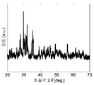
도 1은, 실시예 1에 예시된 공침(co-precipitation) 방법에 의해 제조된, (Ca0.8) (Mg0 .65, Al0 .15) (Si1 .85, Al0 .15)O6 : (Mn2 +)0.2, (Eu2 +)0.2의 XRD 패턴(파장 CuK α의해 측정됨)을 나타낸다.
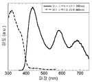
도 2는, 실시예 1에 예시된 공침 방법에 의해 제조된 (Ca0 .8) (Mg0 .65, Al0 .15) (Si1.85, Al0 .15) O6 : (Mn2 +)0.2, (Eu2 +)0.2의, 350 nm 파장 복사선으로 여기 시의 방출 스펙트럼을 나타낸다. 상기 인광체는 대략 680nm, 대략 580 nm 및 대략 440 nm에서 주 발광 최대치를 갖는 광을 방출한다.
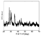
도 3은, 실시예 2에 예시된 공침 방법으로 제조된, (Ca0 .8) (Mg0 .5, Al0 .3) (Si1.7, Al0 .3) O6 : (Mn2 +)0.2, (Eu2 +)0.2의 XRD 패턴(파장 CuK α측정됨)을 나타낸다.
도 4는, 실시예 2에 예시된 공침 방법으로 제조된 (Ca0 .8) (Mg0 .5, Al0 .3) (Si1.7, Al0 .3) O6 : (Mn2 +)0.2, (Eu2 +)0.2의, 350 nm 파장 복사선으로 여기 시의 방출 스펙트럼을 나타낸다. 상기 인광체는 대략 690nm 및 대략 560 nm에서 주 발광 최대치를 갖는 광을 방출한다.
도 5는, 실시예 3에 예시된 마이크로반응 시스템에 의해 제조된, (Ca0 .64, Sr0.16) (Mg0 .65, Al0 .15) (Si1 .85 Al0 .15) O6 : (Mn2 +)0.2, (Eu2 +)0.2의 XRD 패턴(파장 CuK α의해 측정됨)을 나타낸다.
도 6은, 실시예 3에 예시된 마이크로반응 시스템에 의해 제조된 (Ca0 .64, Sr0.16) (Mg0 .65, Al0 .15) (Si1 .85 Al0 .15) O6 : (Mn2 +)0.2, (Eu2 +)0.2의, 350 nm 파장 복사선으로 여기 시의 발광 스펙트럼을 나타낸다. 상기 인광체는 대략 680nm, 대략 570 nm 및 대략 440 nm에서 주 발광 최대치를 갖는 광을 발광한다.
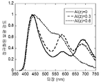
도 7은, 350 nm 파장 복사선으로 여기 시의 (Ca0 .8) (Mg0 .8)Si2O6 : (Mn2 +)0.2, (Eu2+)0.2; (Ca0 .8) (Mg0 .65Al0 .15) (Si1 .85Al0 .15) O6 : (Mn2 +)0.2, (Eu2 +)0.2 및 (Ca0 .8) (Mg0 .5Al0 .3) (Si1 .7Al0 .3) O6 : (Mn2 +)0.2, (Eu2 +)0.2의 발광 스펙트럼을 나타낸다.
도 8은 실시예 1의 발광체 (Ca0 .8) (Mg0 .65, Al0 .15) (Si1 .85, Al0 .15) O6 : (Mn2+)0.2, (Eu2 +)0.2의 적분된 발광 강도를, 비교 실시예(CaMgSi2O6: Eu2+,Mn2+)의 적분된 발광 강도와 비교하여 나타낸다.Figure 1 is prepared by co-precipitation (co-precipitation) method illustrated in Example 1, (Ca 0.8) (Mg 0 .65,
2 is manufactured by a co-precipitation method illustrated in Example 1 (Ca 0 .8) (Mg 0 .65,
3 is manufactured by a co-precipitation method illustrated in Example 2, (Ca 0 .8) ( Mg 0 .5,
Figure 4 is produced by a co-precipitation method illustrated in Example 2 (Ca 0 .8) (Mg 0 .5,
FIG. 5 is a graph showing the relationship between (Ca 0 .64 , Sr 0.16 ) (Mg 0 .65 , Al 0 .15 ) (Si 1 .85 Al 0 .15 ) O 6 : XRD pattern (measured by the wavelength Cu K alpha ) of (Mn 2 + ) 0.2 and (Eu 2 + ) 0.2 .
6 is produced by the microreactor system illustrated in example 3 (Ca 0 .64, Sr 0.16 ) (
Figure 7, when excited by 350 nm wavelength radiation (Ca 0 .8) (Mg 0 .8) Si 2 O 6 : (Mn 2 +) 0.2, (Eu 2+) 0.2; (Ca 0 .8) (Mg 0 .65
8 is a luminous material of Example 1 (Ca 0 .8) (Mg 0 .65,
본 발명의 바람직한 실시양태에서, 화학식 I의 화합물은 하기 화학식 Ia의 화합물로부터 선택된다:In a preferred embodiment of the invention, the compounds of formula (I) are selected from compounds of formula
(M1 -x-u-p,)(Mg1 -z-v-q, Alz -m) (Si2 -z,Tz -n)O6 : Ax, By, Cw Ia (M 1 -xup,) (Mg 1 -zvq, Al z -m) (Si 2 -z, T z -n) O 6: A x, B y, C w Ia
상기 식에서, M, T, A, B 및 C는, 상기 화학식 I에 전술된 바와 동일한 의미를 갖고, Wherein M, T, A, B, and C have the same meanings as described above in formula (I)
m + n + q + p = w이고, 이때 m ≥ 0, n ≥ 0, p ≥ 0, 및 q ≥ 0이고,m + n + q + p = w where m? 0, n? 0, p? 0, and q?
u + v = y이고, 이때 v ≥ 0, u ≥ 0이고, u + v = y, where v? 0, u? 0,
0 ≤ w < 0.3이고,0 < w < 0.3,
0 ≤ x < 0.5이고, 0 < x < 0.5,
0 ≤ y < 0.5이고, 이때 지수 w, x 및 y 중 2개 이상은 0 초과여야 하고,0 < y < 0.5, wherein at least two of the exponents w, x and y must be greater than 0,
0 < z < 0.5이다.0 < z < 0.5.
바람직하게는, 화학식 I의 화합물은 화학식 Ia의 화합물로부터 선택되고, 이때 T는 Al을 나타내고/내거나, w = 0이고/이거나, A는 Eu2 +를 나타내고/내거나, B는 Mn2+를 나타낸다.Preferably, the compound of formula (I) is selected from compounds of formula Ia, wherein T represents the Al / naegeona, w = 0, and / or, A represents an Eu 2 + / naegeona, B represents the Mn 2+ .
더욱 바람직하게는, 본 발명에 따른 화합물은 하기 화학식 Ia-1 내지 Ia-7의 화합물의 군으로부터 선택된다:More preferably, the compounds according to the invention are selected from the group of compounds of the formulas Ia-1 to Ia-7:
((SrsBarCat)1-x-u)(Mg1 -z- v,Alz) (Si2 - z,Alz)O6 : (Eu2 +)x, (Mn2+)y Ia-1 ((Sr s Ba r Ca t ) 1-xu) (Mg 1 -z- v, Al z) (Si 2 - z, Al z) O 6: (Eu 2 +) x, (Mn 2+) y Ia -One
((CatBar)1-x-u)(Mg1 -z-v,Alz) (Si2 -z,Alz)O6 : (Eu2 +)x, (Mn2 +)y Ia-2 ((Ca t Ba r) 1 -xu) (Mg 1 -zv, Al z) (Si 2 -z, Al z) O 6: (Eu 2 +) x, (Mn 2 +) y Ia-2
((SrsBar)1-x-u)(Mg1 -z-v,Alz) (Si2 -z,Alz)O6 : (Eu2 +)x, (Mn2 +)y Ia-3((Sr Ba r s) 1-xu) O 6 (1 -zv Mg, Al z) (-z 2 Si, Al z): (Eu + 2) x, (Mn + 2) y 3-Ia
((SrsCat) 1-x-u)(Mg1 -z-v,Alz) (Si2 -z,Alz)O6 : (Eu2 +)x, (Mn2 +)y Ia-4 ((Sr s Ca t) 1 -xu) (Mg 1 -zv, Al z) (Si 2 -z, Al z) O 6: (Eu 2 +) x, (Mn 2 +) y Ia-4
(Sr1 -x-u)(Mg1 -z-v,Alz) (Si2 -z,Alz)O6 : (Eu2 +)x, (Mn2 +)y Ia-5 (Sr 1 -xu) (Mg 1 -zv, Al z) (Si 2 -z, Al z) O 6: (Eu 2 +) x, (Mn 2 +) y Ia-5
(Ba1 -x-u)(Mg1 -z-v,Alz) (Si2 -z,Alz)O6 : (Eu2 +)x, (Mn2 +)y Ia-6 (Ba 1 -xu) (Mg 1 -zv, Al z) (Si 2 -z, Al z) O 6: (Eu 2 +) x, (Mn 2 +) y Ia-6
(Ca1 -x-u)(Mg1 -z-v,Alz) (Si2 -z,Alz)O6 : (Eu2 +)x, (Mn2 +)y Ia-7 (Ca 1 -xu) (Mg 1 -zv, Al z) (Si 2 -z, Al z) O 6: (Eu 2 +) x, (Mn 2 +) y Ia-7
상기 식에서,In this formula,
0 < r < 1; 0 < s < 1; 0 < t < 1이고; 이때 r + s + t = 1이고,0 < r <1; 0 < s <1; 0 < t <1; Where r + s + t = 1,
u + v = y이고, 이때 v ≥ 0 및 u ≥ 0이고, 지수 u 및 v 중 하나 이상은 0 초과여야 하고,u + v = y, where v? 0 and u? 0, at least one of the exponents u and v must be greater than 0,
0.1 < x < 0.3이고, 0.1 < x < 0.3,
0.1 < y < 0.3이고,0.1 < y < 0.3,
0.05 < z < 0.4이다.0.05 < z < 0.4.
특히 바람직한 화합물은 화학식 Ia-1, Ia-2, Ia-4 및 Ia-7의 화합물의 군, 더욱 바람직하게는 화학식 Ia-2, Ia-4 및 Ia-7의 화합물의 군으로부터 선택되고, 이때 x, y 둘 모두는 0.15 내지 0.2이고/이거나 u는 0이다.Particularly preferred compounds are selected from the group of compounds of formulas Ia-1, Ia-2, Ia-4 and Ia-7, more preferably from the group of compounds of formulas Ia-2, Ia-4 and Ia-7, both x and y are 0.15 to 0.2 and / or u is zero.
특히 바람직한 화합물은 하기 화학식 Ia-2a, Ia-4a 및 Ia-7a의 화합물의 군으로부터 선택된다: Particularly preferred compounds are selected from the group of compounds of the formulas Ia-2a, Ia-4a and Ia-7a:

상기 식에서,In this formula,
0 < r < 1; 0 < s < 1; 0 < t < 1이고, 바람직하게는 0.75 < r < 1; 0 < s < 0.25; 0 < t < 0.25이되, 단 r + t = 1이고, s + t = 1이고, 0 < r <1; 0 < s <1; 0 < t < 1, preferably 0.75 < r < 0 < s <0.25; 0 < t < 0.25, provided that r + t = 1, s + t =
0.075 < z < 0.3이다.0.075 < z < 0.3.
본 발명에 따른 화합물은, 상기 자외선 또는 근자외선을 더 긴 파장, 바람직하게는 VIS 광 범위로 변환하는데 특히 적절하다. The compounds according to the invention are particularly suitable for converting said ultraviolet or near ultraviolet radiation to longer wavelengths, preferably VIS light ranges.
본원 문맥에서, 용어 "자외선(UV radiation)"은, 달리 명백히 기술하지 않는 한, 대략 100 nm 내지 대략 280 nm의 범위의 파장을 갖는 전자기 복사선의 의미를 갖는다. In the present context, the term "UV radiation " has the meaning of electromagnetic radiation having a wavelength in the range of approximately 100 nm to approximately 280 nm, unless expressly stated otherwise.
또한, 용어 "근자외선(near UV radiation)"은, 달리 명백히 기술하지 않는 한, 대략 280 nm 내지 대략 400 nm의 범위의 파장을 갖는 전자기 복사선의 의미를 갖는다. In addition, the term " near UV radiation " has the meaning of electromagnetic radiation having a wavelength in the range of about 280 nm to about 400 nm, unless explicitly stated otherwise.
또한, 용어 "VIS 광 또는 VIS-광 영역"은, 달리 명백히 기술하지 않는 한, 대략 400 nm 내지 대략 800 nm의 범위의 파장을 갖는 전자기 복사선의 의미를 갖는다. In addition, the term "VIS light or VIS-light region" has the meaning of electromagnetic radiation having a wavelength in the range of approximately 400 nm to approximately 800 nm, unless expressly stated otherwise.
본원 문맥에서, 용어 "변환 인광체(conversion phosphor)" 및 용어 "인광체"는 동일한 의미로 사용된다. In the present context, the terms " conversion phosphor "and the term" phosphor "are used interchangeably.
바람직하게는, 본 발명에 따른 화합물은 전형적으로, 근자외선 스펙트럼 범위, 바람직하게는 약 280 내지 약 400 nm에서, 인공 또는 자연 복사선원에 의해 여기된다. 따라서, 본 발명은 또한, 화학식 I의 화합물의 변환 인광체, 또는 간단히 "인광체"로서의 용도에 관한 것이다.Preferably, the compounds according to the invention are typically excited by artificial or natural radiation sources, in the near-ultraviolet spectrum range, preferably from about 280 to about 400 nm. The invention therefore also relates to the use of the compounds of formula I as conversion phosphors, or simply as "phosphors ".
인공적인 "복사선원(radiation source)" 또는 "광원(light source)"은 바람직하게는 불가시광선(black light), 단파장 자외선 램프(short wave ultraviolet lamp), 가스-방전 램프(gas-discharge lamp), 자외선-LED, 근자외선 LED 또는 자외선-레이저로부터 선택된다. Artificial " radiation source "or" light source "is preferably a light source such as a black light, a short wave ultraviolet lamp, a gas- Ultraviolet-LED, near ultraviolet LED or ultraviolet-laser.
본원 문맥에서, 용어 "자연(natural) 복사선원"은 태양 복사선(irradiation) 또는 태양광(sunlight)을 의미한다.In the present context, the term "natural radiation source" means solar radiation or sunlight.
복사선원의 방출 스펙트럼과 본 발명의 화합물의 흡수 스펙트럼이 10 면적% 초과, 바람직하게는 30 면적% 초과, 더욱 바람직하게는 60 면적% 초과, 가장 바람직하게는 90 면적% 초과인 것이 바람직하다. It is preferred that the emission spectrum of the radiation source and the absorption spectrum of the compound of the present invention are greater than 10% area, preferably greater than 30% area, more preferably greater than 60% area, most preferably greater than 90% area.
용어 "흡수(absorption)"는 물질의 흡수성을 의미하고, 이는 물질 상에 떨어지는 복사선 대 물질을 통과하는 복사선의 로그함수 비에 해당된다.The term "absorption" refers to the absorbency of a material, which means that the radiation that falls on the material versus the logarithmic function .
용어 "방출(emission)"은, 원자 및 분자에서의 전자 전이에 의한 전자기파의 방출을 의미한다.The term "emission" refers to the emission of electromagnetic waves due to electron transfer in atoms and molecules.
바람직하게는, 본 발명에 따른 인광체는, 자외선 또는 근자외선 광에 의해 여기되면서도 VIS 광 영역에서 2개 이상의 방출 피크를 나타낸다. 바람직하게는, 첫번째 방출 피크는 바람직하게는 약 400 nm 내지 약 500 nm, 더욱 바람직하게는 약 420 nm 내지 약 480 nm의 방출 최대치를 갖고, 두번째 방출 피크는 바람직하게는 약 550 nm 내지 약 625 nm, 더욱 바람직하게는 약 560 nm 내지 약 600 nm의 방출 최대치를 갖는다. Preferably, the phosphor according to the invention exhibits two or more emission peaks in the VIS light region while being excited by ultraviolet or near-ultraviolet light. Preferably, the first emission peak preferably has an emission maximum of from about 400 nm to about 500 nm, more preferably from about 420 nm to about 480 nm, and the second emission peak preferably has a wavelength of from about 550 nm to about 625 nm , More preferably from about 560 nm to about 600 nm.
또 다른 바람직한 실시양태에서, 본 발명에 따른 인광체는, 자외선 또는 근자외선 광에 의해 여기되면서 VIS 광 영역에서 3개 이상의 방출 피크를 나타낸다. 첫번째 방출 피크는 각각, 약 400 nm 내지 약 500 nm, 더욱 바람직하게는 약 420 nm 내지 약 480 nm의 범위의 방출 최대치를 갖고, 제2 방출 피크는 약 550 nm 내지 625 nm, 더욱 바람직하게는 약 560 nm 내지 약 600 nm의 범위의 방출 최대치를 갖고, 세번째 방출 피크는 약 625 nm 내지 약 790 nm, 더욱 바람직하게는 약 650 nm 내지 약 720 nm 범위의 방출 최대치를 갖는다. In another preferred embodiment, the phosphor according to the present invention exhibits three or more emission peaks in the VIS light region, being excited by ultraviolet or near-ultraviolet light. The first emission peak has an emission maximum in the range of about 400 nm to about 500 nm, more preferably in the range of about 420 nm to about 480 nm, the second emission peak is in the range of about 550 nm to about 625 nm, Has an emission maximum in the range of 560 nm to about 600 nm and the third emission peak has an emission maximum in the range of about 625 nm to about 790 nm, more preferably about 650 nm to about 720 nm.
본 발명에 따른 화합물의 방출 피크는, 바람직하게는 서로 중첩된다. 바람직하게는 중첩은 90 면적% 미만, 더욱 바람직하게는 60 면적% 미만, 더욱 더 바람직하게는 30 면적% 미만이다.The emission peaks of the compounds according to the invention are preferably superimposed on one another. Preferably, the overlap is less than 90 area%, more preferably less than 60 area%, even more preferably less than 30 area%.
본 발명의 화합물 내의 Al의 양(특히 변수 z와 관련하여)을 변화시킴으로써, 약 550 nm 내지 약 625 nm의 범위의 방출 최대치를 갖는 방출 피크 및 625 nm 내지 약 790 nm의 범위의 방출 최대치를 갖는 방출 피크의 상대 강도가 제어될 수 있다. By varying the amount of Al in the compound of the present invention (particularly with respect to the variable z), it is possible to have an emission peak having an emission maximum in the range of about 550 nm to about 625 nm and an emission peak in the range of 625 nm to about 790 nm The relative intensity of the emission peak can be controlled.
따라서, Al 함량을 변화시킴으로써 인광체의 방출 색을 변화시킬 수 있다. 일반적으로, z 값이 더 커질수록, 약 550 nm 내지 약 625 nm의 범위의 주 발광 최대치를 갖는 방출 피크의 강도가 커지고, 약 625 nm 내지 약 790 nm의 범위의 주 발광 최대치를 갖는 방출 피크의 강도는 작아진다.Therefore, the emission color of the phosphor can be changed by changing the Al content. Generally, the greater the z value, the greater the intensity of the emission peak having a main emission maximum in the range of about 550 nm to about 625 nm, and the higher the emission peak in the range of about 625 nm to about 790 nm The strength becomes smaller.
따라서, 본 발명의 바람직한 화합물은 바람직하게는 하기 하위화학식의 화합물로부터 선택된다:Accordingly, preferred compounds of the present invention are preferably selected from compounds of the sub-formulas:


![]()
![]()
상기 식에서, 0 < r < 1; 0 < s < 1; 0 < t < 1, 바람직하게는 0.75 < r < 1; 0 < s < 0.25; 0 < t < 0.25이고, 이때 r + t = 1, 및 s + t = 1이다.Wherein 0 < r <1; 0 < s <1; 0 < t < 1, preferably 0.75 < r < 0 < s <0.25; 0 < t < 0.25, where r + t = 1 and s + t = 1.
본 발명에 따른 화합물의 제조를 위한 출발 물질은 상업적으로 수득가능하고, 본 발명에 따른 화합물의 제조에 적합한 공정은 2개의 일반적인 공정 유형으로 요약될 수 있다. 첫번째는, 고상 확산 공정(solid state diffusion process)이고, 두번째는 습식-화학 공정(wet-chemical process)이다. Starting materials for the preparation of the compounds according to the invention are commercially obtainable and processes suitable for the preparation of the compounds according to the invention can be summarized in two general process types. The first is a solid state diffusion process and the second is a wet-chemical process.
본원 문맥에서, 용어 "고상 확산 공정"은, Mg, Al, M의 산화물과, A, B 또는 C로부터 선택되는 2개 이상의 원소를 포함하는 하나 이상의 염을 사전 결정된 몰 비로 혼합시키는 단계, 임의적으로 상기 혼합물을 분쇄(grinding)하는 단계, 및 1500℃ 이하의 온도에서 로(furnace) 내에서, 임의적으로 환원 대기 하에서, 며칠 동안 분말을 하소(calcining)시키는 단계(문헌[Phosphor Handbook, second edition, CRC Press, 2006, 341-354] 참조)를 포함하는, 임의의 혼합 및 소성 방법 또는 고상 방법을 지칭한다. In the context of the present application, the term " solid phase diffusion process "includes mixing at least one salt comprising oxides of Mg, Al, M and two or more elements selected from A, B or C at a predetermined molar ratio, Grinding the mixture and calcining the powder for several days under a reducing atmosphere, optionally in a furnace at temperatures below 1500 DEG C (Phosphor Handbook, second edition, CRC Press, 2006, 341-354). ≪ / RTI >
본원 문맥에서, 용어 "습식-화학 공정"은 바람직하게는, In the context of the present application, the term "wet-chemical process"
a) 규소 함유 물질, 적어도 Mg, Al, M 원소를 포함하는 염의 혼합물, 및 A, B 또는 C로부터 선택되는 2개 이상의 원소를 포함하는 하나 이상의 염을 사전결정된 몰 비로 용매 중에서 혼합시키는 단계;a) mixing at least one salt comprising a silicon-containing material, a mixture of salts comprising at least Mg, Al and M elements, and two or more elements selected from A, B or C in a solvent in a predetermined molar ratio;
b) 침전제를 가하는 단계;b) adding a precipitant;
c) 혼합물에 대해 산화성 대기 하에서 800 내지 1300℃의 온도 범위로 1차 열처리하는 단계; 및c) subjecting the mixture to a first heat treatment in a temperature range of 800 to 1300 占 폚 under an oxidizing atmosphere; And
d) 상기 혼합물에 대해 환원성 대기 하에서 800 내지 1300℃의 온도 범위로 2차 열처리하는 단계d) subjecting the mixture to a secondary heat treatment in a temperature range of 800 to 1300 캜 under a reducing atmosphere
를 포함한다. .
단계 c) 및/또는 d)의 전술된 가열 처리는 바람직하게는 1000℃ 초과의 온도, 더욱 바람직하게는 1100℃ 내지 1300℃의 범위에서 수행된다. The above-mentioned heat treatment of step c) and / or d) is preferably carried out at a temperature of more than 1000 ° C, more preferably in a range of 1100 ° C to 1300 ° C.
용어 "환원성 대기"는 환원 특성을 갖는 대기, 바람직하게는 질소 스트림(바람직하게는 N2/H2의 스트림 및 특히 바람직하게는 N2/H2(95 - 80 : 5 - 20)의 스트림) 중에서 가스 또는 수소 또는 적어도 진공 또는 산소-결핍 대기를 형성하는, 바람직하게는 일산화탄소의 대기를 의미한다.The term "reducing atmosphere" refers to an atmosphere, preferably a nitrogen stream (preferably a stream of N 2 / H 2 and particularly preferably a stream of N 2 / H 2 (95 - 80: 5 - 20) Means a gas or hydrogen, or at least an atmosphere of carbon monoxide, which forms at least a vacuum or oxygen-deficient atmosphere.
용어 "산화성 대기"는 산화 특성을 갖는 대기, 바람직하게는 공기 또는 산소 대기의 의미를 갖는다. The term "oxidizing atmosphere" has the meaning of an atmosphere, preferably an air or oxygen atmosphere, having oxidation characteristics.
단계 a)는 바람직하게는, 마이크로 반응기, 1 mm 내지 10 mm 너비 범위의 내부 지름을 갖는 작은 한정된 영역의 유동 채널에서 수행되고, 이때 상기 유동 채널을 통해 둘 이상의 용액이 혼합된다. 상기 마이크로 반응기에서, 혼합된 용액의 화학적 반응은 몇 밀리미터 미만의 통상적인 측방향 치수의 구획에서 일어난다. Step a) is preferably carried out in a microreactor, in a small confined region of flow channels with an inner diameter in the range of 1 mm to 10 mm width, wherein two or more solutions are mixed through the flow channel. In the microreactor, the chemical reaction of the mixed solution takes place in a section of conventional lateral dimensions of less than a few millimeters.
상기 인광체의 실제 조성 비는 파장 분산 X-선 분광법(WDX)에 의해 확인될 수 있고, WDX의 결과를 사용하여 상기 혼합 단계 a)에서의 원소 Mg, Al, M, A, B 및 C를 포함하는 염의 몰 비를 사전결정할 수 있다.The actual composition ratios of the phosphors can be confirmed by wavelength dispersive X-ray spectroscopy (WDX) and include the elements Mg, Al, M, A, B and C in the mixing step a) Can be determined in advance.
상기 단계 a)에서의 혼합물의 제조를 위해, 상기 염 또는 성분들의 일부 또는 전부의 혼합물을 분말로서 제조하고 용매를 가하거나, 상기 혼합물을 용매 중에서 직접 단계적으로 제조할 수 있다. 하지만, 침전 단계 전(단계 b) 전) 어느 때에나 전술된 염이 가해질 수 있다.For the preparation of the mixture in step a), the salt or a mixture of some or all of the components may be prepared as a powder and a solvent added, or the mixture may be prepared stepwise directly in a solvent. However, the above-mentioned salts may be applied at any time before the precipitation step (step b).
"규소-함유 물질(silicon containing agent)"이라는 용어는, 무기 규소 화합물, 바람직하게는 화학식 SiO2를 갖는 규소의 산화물을 포함한다. 이는 비결정질 형태뿐만 아니라 다수의 다른 결정질 형태(다형체)를 가진다. SiO2는 1 μm 미만의 직경을 갖는 작은 입자여야 하며, 200 nm 미만의 직경이 더 바람직하다. 규소-함유 물질은 또한 임의의 유기 규소 화합물을 지칭하며, 예컨대 테트라알킬 오르쏘-실리케이트(다르게는, 테트라알콕시 실란으로도 공지됨), 바람직하게는 테트라에톡시실란 또는 테트라메톡시실란이다.The term "silicon-containing material (silicon containing agent)" is to include inorganic silicon compound, preferably comprises an oxide of silicon having the formula SiO 2. It has many different crystalline forms (polymorphs) as well as amorphous forms. SiO 2 should be small particles having a diameter of less than 1 μm, more preferably less than 200 nm in diameter. The silicon-containing material also refers to any organosilicon compound, such as tetraalkyl orthosilicate (otherwise known as tetraalkoxysilane), preferably tetraethoxysilane or tetramethoxysilane.
원소 Mg, Al, M, A, B 및 C의 적합한 염은 바람직하게는 상응하는 나이트레이트, 할로게나이드, 하이드로겐설페이트 또는 카보네이트, 더욱 바람직하게는 나이트레이트 또는 할로게나이드, 가장 바람직하게는 할로게나이드, 특히 클로라이드로부터 선택된다. Suitable salts of the elements Mg, Al, M, A, B and C are preferably the corresponding nitrates, halogenides, hydrogen sulphates or carbonates, more preferably nitrates or halogens, 0.0 > chloride, < / RTI >
용어 "용매"는 Si-화합물을 반드시 용해시키지는 않는 용매를 의미한다. 물과 알코올, 예컨대 메탄올, 에탄올 등이 본 발명에 따른 바람직한 용매이다. The term "solvent" means a solvent which does not necessarily dissolve the Si-compound. Water and alcohols such as methanol, ethanol and the like are preferred solvents according to the present invention.
단계 b)에서의 바람직한 침전제는 바람직하게는 나트륨 하이드로겐 카보네이트, 암모늄 클로라이드, 또는 암모늄 하이드로겐 카보네이트로부터 선택되고, 더욱 바람직하게는 상기 침전제는 암모늄 클로라이드이다.The preferred precipitant in step b) is preferably selected from sodium hydrogencarbonate, ammonium chloride, or ammonium hydrogencarbonate, more preferably the precipitant is ammonium chloride.
본 발명의 바람직한 실시양태에서, 상기 침전제는 적합한 용매 중에 첨가되고, 바람직하게는 상응하는 용매의 융점 이상이고 용매의 비점 이하인 온도에서 용매와 혼합된다. 더욱 바람직하게는 약 70℃ 이하, 더욱 더 바람직하게는 약 60℃ 이하의 온도 범위에서, 바람직하게는 약 1 시간 이상, 더욱 바람직하게는 약 2 시간 이상 동안 수행된다.In a preferred embodiment of the present invention, the precipitant is added to a suitable solvent and is preferably mixed with the solvent at a temperature above the melting point of the corresponding solvent and below the boiling point of the solvent. More preferably about 70 DEG C or less, and even more preferably about 60 DEG C or less, preferably about 1 hour or more, and more preferably about 2 hours or more.
본 발명의 바람직한 실시양태에서, 예비-가열 처리 단계는 임의적으로, 단계 b)의 혼합물로부터 용매를 증발시키기 위해, 단계 b)를 수행한 이후 단계 c)를 수행하기 이전에 수행될 수 있다. 당업계 숙련자에게 통상적으로 공지된 바와 같이, 적합한 온도 조건은 사용된 용매에 따라 주로 결정된다. 하지만, 바람직한 온도 조건은 100℃ 이하이고, 더욱 바람직하게는 90℃ 이하이고, 더욱 더 바람직하게는 80℃ 이하이다. In a preferred embodiment of the present invention, the pre-heat treatment step may optionally be performed prior to performing step c) after performing step b) to evaporate the solvent from the mixture of step b). As is commonly known to those skilled in the art, suitable temperature conditions are determined primarily by the solvent used. However, the preferable temperature condition is 100 DEG C or lower, more preferably 90 DEG C or lower, even more preferably 80 DEG C or lower.
적합한 증발 대기는, 압력 또는 대기와 관련된 임의의 특정 조건에 특별히 한정되지 않는다. 하지만, 바람직하게는 용매의 증발은 공기 대기 하에서 수행되고, 또한 감압 조건을 적용하는 것도 본 발명에 적용가능하다.A suitable evaporation atmosphere is not particularly limited to any particular conditions associated with pressure or atmosphere. Preferably, however, evaporation of the solvent is carried out in an air atmosphere, and application of a reduced pressure condition is also applicable to the present invention.
단계 c)와 관련하여, 당업계 숙련자에게 공지된 바와 같이, 어닐링 오븐은, 바람직하게는 산화성 대기(예컨대 산소 또는 공기 또는 산소-함유 대기) 하에서 작동된다. 본 발명의 추가의 바람직한 실시양태에서, 통상적으로 공지된 산화 로가 단계 c)에서 사용된다.With regard to step c), as is known to those skilled in the art, the annealing oven is preferably operated under an oxidizing atmosphere (such as oxygen or air or an oxygen-containing atmosphere). In a further preferred embodiment of the present invention, a conventionally known oxidation furnace is used in step c).
단계 d)와 관련하여, 당업계 숙련자에게 공지된 바와 같이, 어닐링 오븐은, 바람직하게는 환원성 대기(예컨대 일산화탄소, 순수 수소, 진공, 또는 산소-결핍 대기) 하에서 작동된다. 본 발명의 추가의 바람직한 실시양태에서, 통상적으로 공지된 환원 로가 단계 d)에서 사용된다.With regard to step d), the annealing oven is preferably operated under a reducing atmosphere (such as a carbon monoxide, a pure hydrogen, a vacuum, or an oxygen-deficient atmosphere), as is known to those skilled in the art. In a further preferred embodiment of the present invention, a conventionally known reduction reactor is used in step d).
본 발명에 따른 인광체의 입자 크기는 전형적으로 50 nm 내지 30 μm, 바람직하게는 1 μm 내지 20 μm이다.The particle size of the phosphor according to the invention is typically 50 nm to 30 μm, preferably 1 μm to 20 μm.
추가의 바람직한 실시양태에서, 입자 형태의 인광체는 SiO2, TiO2, Al2O3, ZnO, ZrO2 및/또는 Y2O3 또는 이들의 혼합된 산화물로 이루어진 연속적인 표면 코팅을 갖는다. 상기 표면 코팅은, 코팅 물질의 적합한 등급의 굴절 지수에 의해, 상기 굴절 지수가 환경에 매칭될 수 있다는 장점이 있다. 이러한 경우, 인광체의 표면에서 광의 산란은 감소하고, 더 큰 비율의 광이 인광체 내로 침투되고, 흡수되고, 그 안에서 변환될 수 있다. 또한, 상기 굴절지수-매칭된 표면 코팅은 총 내부 반사가 감소하기 때문에 인광체의 외부에 더 많은 광이 커플링될 수 있게 한다.In a further preferred embodiment, the phosphor in particle form is selected from the group consisting of SiO 2 , TiO 2 , Al 2 O 3 , ZnO, ZrO 2 and / or Y 2 O 3 or a mixed oxide thereof. The surface coating has the advantage that the index of refraction can be matched to the environment by a refractive index of a suitable grade of the coating material. In this case, scattering of light at the surface of the phosphor is reduced, and a greater proportion of light can be penetrated into the phosphor, absorbed, and converted therein. In addition, the refractive index-matched surface coating allows more light to be coupled to the exterior of the phosphor as the total internal reflection decreases.
또한, 인광체가 캡슐화되어야 하는 경우에 연속적인 층이 유리하다. 이는, 즉각적인 환경에서 확산하는 물 또는 다른 물질에 대한 인광체 또는 이의 부분의 민감성을 억제하기 위해 필요할 수 있다. 밀폐된 쉘로 캡슐화하는 추가의 이유는, 칩 내에서 발생된 열에 의해 실제 인광체가 열적 탈커플링(thermal decoupling)되기 때문이다. 상기 열은 인광체의 형광 수율을 감소시키는 결과를 낳고, 또한 형광의 색상에 영향을 줄 수 있다. 마지막으로, 이러한 유형의 코팅은, 인광체에서 발생되는 격자 진동이 주변 환경으로 전파되는 것을 방지함으로써 인광체의 효율을 증가시킨다.Also, a continuous layer is advantageous when the phosphor is to be encapsulated. This may be necessary to suppress the sensitivity of the phosphor or portion thereof to water or other materials diffusing in an immediate environment. A further reason for encapsulation with a closed shell is that the actual phosphor is thermally decoupled by the heat generated within the chip. This heat results in a decrease in the phosphor yield of the phosphor and can also affect the color of the fluorescence. Finally, this type of coating increases the efficiency of the phosphor by preventing lattice vibrations occurring in the phosphor from propagating to the environment.
또한, 상기 인광체가 SiO2, TiO2, Al2O3, ZnO, ZrO2 및/또는 Y2O3 또는 이들의 혼합된 옥사이드 또는 인광체 조성물로 이루어진 다공성 표면 코팅을 갖는 것이 바람직하다. 이러한 다공성 코팅은 단일 층의 굴절 지수를 추가로 감소시키는 가능성을 제공한다. 이러한 유형의 다공성 코팅은 WO 03/027015에 기술된 3가지 통상적인 방법, 즉 유리(예컨대, 소다-석회 유리(US 4019884 참조))의 에칭(etching), 다공성 층의 적용, 및 다공성 층과 에칭 작용의 조합에 의해 제조될 수 있고, 이를 전체범위로 본원에 참고로 인용한다.Further, it is desirable to have a porous surface coating the phosphor is composed of SiO 2, TiO 2, Al 2 O 3, ZnO, ZrO 2 and / or Y 2 O 3 or a mixed oxide or phosphor composition. This porous coating offers the possibility of further reducing the refractive index of a single layer. This type of porous coating can be applied by three conventional methods described in WO 03/027015, namely etching of glass (e.g., soda-lime glass (cf. US 4019884)), application of a porous layer, ≪ / RTI > and are incorporated herein by reference in their entirety.
추가의 바람직한 실시양태에서, 상기 인광체 입자는, 바람직하게는 에폭시 또는 실리콘 수지로 이루어진, 환경에 대한 화학 결합을 용이하게 하는 작용기를 함유하는 표면을 갖는다. 이들 작용기는, 예를 들어, 에스터 또는 다른 유도체일 수 있으며, 이들은 옥소 기를 통해 결합되고 에폭사이드 및/또는 실리콘 기반의 결합제의 구성 성분에 대한 결합을 형성할 수 있다. 이러한 유형의 표면은, 인광체를 결합제 내로 균질하게 혼입시키는 것을 용이하게 하는 장점이 있다. 또한, 인광체/결합제 시스템의 유변학적(rheological) 특성 및 또한 포트 수명은 이로써 특정한 정도로 조절될 수 있다. 따라서 혼합물의 공정이 간소화된다.In a further preferred embodiment, the phosphor particles have a surface comprising a functional group which facilitates chemical bonding to the environment, preferably consisting of an epoxy or silicone resin. These functional groups can be, for example, esters or other derivatives, which can be bonded through oxo groups and form bonds to the components of the epoxide and / or silicon based binder. This type of surface has the advantage of facilitating homogeneous incorporation of the phosphor into the binder. In addition, the rheological properties of the phosphor / binder system as well as the port life can thereby be adjusted to a certain degree. Thus simplifying the process of the mixture.
LED 칩에 적용된 본 발명에 따른 인광체 층은 바람직하게는, 벌크 주조(bulk casting)에 의해 적용되는, 실리콘 및 균질 인광체 입자의 혼합물로 이루어지고 상기 실리콘은 표면 장력을 갖기 때문에, 상기 인광체 층은 미시적 수준에서 균일하지 않거나 층의 두께가 전체적으로 일정하지 않다. 이는 일반적으로 또한, 인광체가 벌크-주조 공정에 의해 적용되지 않고 대신에 소위 칩-수준 변환 공정(여기서는, 고도로 농축된 얇은 인광체층이 정전기적 방법의 도움으로 칩의 표면에 직접적으로 적용된다)에 의해 적용되는 경우에 그러하다.The phosphor layer according to the present invention applied to the LED chip preferably comprises a mixture of silicon and homogeneous phosphor particles, applied by bulk casting, and since the silicon has surface tension, the phosphor layer is microscopic Level is not uniform or the thickness of the layer is not uniform throughout. This generally also means that the phosphor is not applied by the bulk-cast process and instead is applied to the so-called chip-level conversion process (here a highly concentrated thin phosphor layer is applied directly to the surface of the chip with the aid of an electrostatic process) And so on.
전술된 방법의 도움으로, 인광체 입자, 예컨대 구형 입자, 플레이크 및 구조화된 물질 및 세라믹의 임의의 바람직한 외부 형상을 제조하는 것이 가능하다.With the aid of the above-described method, it is possible to produce any desired external shape of the phosphor particles, such as spherical particles, flakes and structured materials and ceramics.
추가의 바람직한 실시양태로서의 플레이크형 인광체의 제조는, 상응하는 금속 염 및/또는 희토류 염으로부터 통상적인 방법에 의해 수행된다. 이 제조 방법은 EP 763573 및 DE 102006054331에 자세히 기술되어 있고, 이들을 참조로써 본원에 이의 전체 범위로 인용한다. 이러한 플레이크형 인광체는, 예컨대, 운모, SiO2, Al2O3, ZrO2, 유리 또는 TiO2 플레이크(이는 매우 큰 종횡비, 원자적으로 평활한 표면(atomically smooth surface), 및 조절가능한 두께를 가짐)를 포함하는 천연 또는 인공적으로 제조된 고안정성 지지체 또는 기판을, 수성 분산액 또는 현탁액 중의 침전 반응에 의해, 인광체 층으로 코팅함으로써 제조될 수 있다. 운모, ZrO2, SiO2, Al2O3, 유리 또는 TiO2 또는 이들의 혼합물 외에도, 상기 플레이크는 또한 인광체 물질 자체로 이루어지거나 또는 하나의 물질로 구성될 수 있다. 플레이크 그 자체가 단지 인광체 코팅을 위한 지지체 역할만을 하는 경우, 인광체 코팅은 LED의 일차적인 복사선에 투과성이거나 일차적인 복사선을 흡수하고 이 에너지를 인광체 층에 전달하는 물질로 이루어져야만 한다. 플레이크형 인광체는 수지(예컨대 실리콘 또는 에폭시 수지) 내에 분산되어 있고, 이 분산액은 LED 칩으로 적용된다. 플레이크형 인광체는 50 nm 내지 약 20 μm, 바람직하게는 150 nm 내지 5 μm의 두께의 큰 공업용 스케일로 제조될 수 있다. 이때 지름은 50 nm 내지 20 μm이다. 이는 일반적으로 1 : 1 내지 400 : 1 및 특히 3 : 1 내지 100 : 1의 종횡비(지름 대 입자 두께의 비율)를 갖는다.The preparation of flaky phosphors as further preferred embodiments is carried out by conventional methods from the corresponding metal salts and / or rare earth salts. This preparation process is described in detail in EP 763573 and DE 102006054331, which are incorporated herein by reference in their entirety. The flake-shaped phosphor is, for example, mica, SiO 2, Al 2 O 3, ZrO 2, glass or TiO 2 flakes (which has a very large aspect ratio, the atomic surface smooth by (atomically smooth surface), and the adjustable thickness By coating with a phosphor layer by a precipitation reaction in an aqueous dispersion or suspension. ≪ RTI ID = 0.0 > [0050] < / RTI > In addition to mica, ZrO 2 , SiO 2 , Al 2 O 3 , glass or TiO 2 or mixtures thereof, the flakes may also consist of the phosphor material itself or of a single material. If the flake itself only serves as a support for the phosphor coating, the phosphor coating must be made of a material which is transparent to the primary radiation of the LED or which absorbs the primary radiation and transfers this energy to the phosphor layer. The flaky phosphor is dispersed in a resin (for example, silicone or epoxy resin), and the dispersion is applied to an LED chip. The flaked phosphors may be produced on a large industrial scale with a thickness of from 50 nm to about 20 μm, preferably from 150 nm to 5 μm. With a diameter of 50 nm to 20 μm. It has an aspect ratio (ratio of diameter to particle thickness) of generally from 1: 1 to 400: 1 and in particular from 3: 1 to 100: 1.
플레이크 치수(길이 x 너비)는 배열에 따라 달라진다. 플레이크는 또한, 특히 작은 치수를 갖는 경우, 변환 층 내의 산란(scattering) 중심으로서 적합하다. The flake dimension (length x width) depends on the array. The flakes are also suitable as scattering centers in the conversion layer, especially with small dimensions.
LED 칩에 닿는 본 발명에 따른 플레이크형 인광체의 표면에는, LED 칩에 의해 방출되는 일차적인 복사선에 대해 반사방지(antireflection) 작용을 하는 코팅이 제공된다. 이는 일차적인 복사선의 후방-산란(back-scattering)을 감소시켜, 일차적인 복사선이 본 발명의 인광체 내로 더 잘 결합되게 한다.The surface of the flaked phosphor according to the present invention touching the LED chip is provided with a coating that antireflects against the primary radiation emitted by the LED chip. This reduces the back-scattering of the primary radiation, allowing the primary radiation to better couple into the phosphors of the present invention.
이러한 목적에 적합한 것은, 예를 들어, 두께 d(이때, d= [LED 칩의 일차적인 복사의 파장/(4* 인광체 세라믹의 굴절 지수)])를 가져야 하는 매칭된 굴절 지수의 코팅이고, 예컨대, 문헌[Gerthsen, Physik [Physics], Springer Verlag, 18th Edition, 1995]을 참조할 수 있다. 상기 코팅은 또한 광자 결정(photonic crystal)으로 이루어질 수 있으며, 이는 특정한 작용기를 수득하기 위해 플레이크형 인광체의 표면을 구조화시키는 것을 포함한다. Suitable for this purpose is, for example, a coating of matched refractive indices which should have a thickness d, where d = [the wavelength of the primary radiation of the LED chip / (4 * the refractive index of the phosphor ceramic) , Gerthsen, Physik [Physics], Springer Verlag, 18th Edition, 1995). The coating may also consist of a photonic crystal, which involves structuring the surface of the flaked phosphor to obtain a specific functional group.
본 발명에 따른 인광체를 세라믹 형태로 제조하는 것은 DE 102006037730(메르크)에 기술된 공정과 유사하게 수행되고, 상기 특허를 참조로써 본원의 문맥에 이의 전체 범위로 인용한다. 이 공정에서, 인광체는, 상응하는 출발 물질 및 도판트를 혼합하고 이어서 등압 프레싱 처리하고, 균질하고 얇고 무공성인 플레이크의 형태의 칩의 표면에 바로 적용됨으로써 습식-화학 방법에 의해 제조된다. 따라서, 인광체의 여기 및 방출의 위치-의존적인 변화가 없고, 이는, 이로써 제공되는 LED가 일정한 색상의 균질한 광원 뿔(light cone)을 방출하고 높은 광 출력을 갖는 것을 의미한다. 세라믹 인광체 바디는 큰 공업적 스케일, 예컨대, 수백 nm 내지 약 500 μm의 두께의 플레이크로 생산될 수 있다. 플레이크 치수(길이 x 너비)는 배열에 따라 달라진다. 칩에 직접적으로 적용되는 경우, 플레이크의 크기는, 적합한 칩 정렬(예컨대 플립-칩(flip-chip) 정렬)로 또는 상응하게, 칩 표면의 약 10% 내지 30%의 특정 오버사이즈로 칩 치수(약 100 μm * 100 μm 내지 수 mm2)에 따라 선택되어야 한다. 인광체 플레이크가 최종 LED 상에 구비되는 경우, 존재하는 광원 뿔 전체가 플레이크를 통과한다. The preparation of the phosphor according to the invention in the form of a ceramic is carried out analogously to the process described in DE 102006037730 (Merck), which is incorporated herein by reference in its entirety. In this process, the phosphors are prepared by a wet-chemical process by mixing the corresponding starting materials and dopants and then isostatically pressing and applying directly to the surface of the chip in the form of homogeneous, thin, nonporous flakes. Thus, there is no position-dependent change in the excitation and emission of the phosphors, which means that the LEDs thus provided emit a uniform light cone of uniform hue and have a high light output. The ceramic phosphor body can be produced on a large industrial scale, e.g., a flake with a thickness of between a few hundred nanometers and about 500 microns. The flake dimension (length x width) depends on the array. When applied directly to the chip, the size of the flakes can be adjusted by suitable chip alignment (e.g., flip-chip alignment) or corresponding chip dimensions (e.g., about 10% to 30% About 100 μm * 100 μm to several mm 2 ). When a phosphorescent flake is provided on the final LED, the entire cone of the existing light source passes through the flake.
세라믹 인광체 바디의 측면이 가벼운 금속 또는 귀금속, 바람직하게는 알루미늄 또는 은으로 코팅될 수 있다. 금속 코팅은, 인광체 바디로부터 광이 측방향으로 나오지 않는 효과를 갖는다. 측방향으로 나오는 광은 LED의 외부에 커플링될 광류(luminous flux)를 감소시킨다. 세라믹 인광체 바디의 금속 코팅은, 막대(rod) 또는 플레이크를 제공하는 등압 프레싱 후의 공정 단계에서 수행되며, 이때 상기 막대 또는 플레이크는 임의적으로 금속 코팅 전에 필요한 크기로 절단될 수 있다. 이를 위해, 측면은 예컨대 질산 은 및 글루코오스를 포함하는 용액으로 습윤되고, 이어서 승온에서 암모니아 대기에 노출된다. 예를 들어 은 코팅은 상기 공정에서 측면 상에 형성된다. The side of the ceramic phosphor body may be coated with a light metal or a noble metal, preferably aluminum or silver. The metal coating has the effect that light does not sideways from the phosphor body. The light coming out in the lateral direction reduces the luminous flux to be coupled to the outside of the LED. The metal coating of the ceramic phosphor body is performed at a process step after isobaric pressing to provide a rod or flake, wherein the bar or flake may optionally be cut to the required size prior to metal coating. To this end, the side is wetted with a solution containing, for example, silver nitrate and glucose, and then exposed to an ammonia atmosphere at elevated temperatures. For example, silver coatings are formed on the sides in the process.
달리, 무전류(current less) 금속화 공정이 또한 적합하다(예컨대, 문헌[Hollemann-Wiberg, Lehrbuch der Anorganischen Chemie [Textbook of Inorganic Chemistry], Walter de Gruyter Verlag or Ullmanns Enzyklopadie der chemischen Technologie [Ullmann's Encyclopaedia of Chemical Technology]]을 참조한다). 세라믹 인광체 바디는, 필요한 경우, 물-유리 용액을 사용하여 LED 칩의 베이스보드(baseboard)에 고정될 수 있다. Alternatively, a current less metallization process is also suitable (see, for example, Hollemann-Wiberg, Lehrbuch der Anorganischen Chemie [Textbook of Inorganic Chemistry], Walter de Gruyter Verlag or Ullmanns Enzyklopadie der chemischen Technologie [Ullmann's Encyclopedia of Chemical Technology]]). The ceramic phosphor body may be secured to the baseboard of the LED chip using a water-glass solution, if desired.
추가의 실시양태에서, 상기 세라믹 인광체 바디는 LED 칩의 양 대향면 상에 구조화된(예컨대 피라미드형) 표면을 갖는다. 이는 가능한 많은 광이 인광체 바디 외부에 커플링되게 한다. 인광체 바디의 구조화된 표면은, 구조화된 압력 판을 갖는 압축 금형을 사용하여 등압 프레싱을 수행하고 이어서 구조체를 표면 내로 엠보싱함으로써 제조될 수 있다. 구조화된 표면은, 가능한 가장 얇은 인광체 바디 또는 플레이크를 생산하기 위한 목적인 경우에 바람직하다. 프레싱 조건은 당업계 숙련자에게 공지되어 있다(문헌[J. Kriegsmann, Technische keramische Werkstoffe [Industrial Ceramic Materials], Chapter 4, Deutscher Wirtschaftsdienst, 1998] 참조). 사용된 프레싱 온도는 프레싱될 물질의 융점의 2/3 내지 5/6인 것이 중요하다.In a further embodiment, the ceramic phosphor body has a structured (e.g., pyramidal) surface on both opposing sides of the LED chip. This allows as much light as possible to be coupled outside the body of the phosphor. The structured surface of the phosphor body can be made by performing isobaric pressing using a compression mold with a structured pressure plate and then embossing the structure into the surface. The structured surface is desirable for the purpose of producing the thinnest phosphor body or flake possible. Pressing conditions are known to those skilled in the art (see J. Kriegsmann, Technische keramische Werkstoffe [Industrial Ceramic Materials], Chapter 4, Deutscher Wirtschaftsdienst, 1998). It is important that the pressing temperature used is 2/3 to 5/6 of the melting point of the material to be pressed.
본 발명에 따른 화합물은 높은 열 켄칭 저항률을 보인다.The compounds according to the invention show a high thermal quenching resistivity.
용어 "열 켄칭 저항률(thermal quenching resistivity)"은 25℃에서의 원래 강도에 비해 더 높은 온도에서의 방출 강도의 감소를 의미한다.The term " thermal quenching resistivity "means a decrease in the emission intensity at higher temperatures relative to the original strength at 25 占 폚.
본 발명의 화합물은 분해와 관련하여 습도 또는 수분에 대해 높은 화학적 안정성을 보인다.The compounds of the present invention exhibit high chemical stability with respect to humidity or moisture with respect to degradation.
본 발명에 따른 화합물은 바람직하게는 80% 이상, 더욱 바람직하게는 90% 이상의 양자 효율을 나타낸다.The compound according to the present invention preferably exhibits a quantum efficiency of 80% or more, more preferably 90% or more.
본 발명의 화합물은 우수한 LED 품질을 갖는다. 본원에서, LED 품질은 통상적으로 공지된 변수, 예컨대 연색 지수(color rendering index (CRI)), 상관 색 온도(Correlated Color Temperature (CCT)), 및 루멘 등가(lumen equivalent) 또는 절대 루멘, 및 CIE x 및 y 좌표에서의 색점에 의해 결정된다.The compounds of the present invention have excellent LED quality. Here, LED quality is typically measured using known parameters such as color rendering index (CRI), Correlated Color Temperature (CCT), and lumen equivalent or absolute lumen and CIE x And the color point in the y coordinate.
당업계에 공지된 바와 같이, 연색 지수(CRI)는, 인공적인 광원의 색 정확도(color fidelity)를 태양광 또는 필라멘트 광원의 색 정확도(이들 두개는 100의 CRI를 가짐)와 비교하는 무-단위(unit less) 광도 측정 크기이다.As is known in the art, the color rendering index (CRI) is a non-unit that compares the color fidelity of an artificial light source with the color accuracy of a sunlight or filament light source (both of which have a CRI of 100) (unit less) is the magnitude of the light measurement.
당업계 숙련자에게 공지된 바와 같이, 상관 색 온도(CCT)는 켈빈(Kelvin) 단위를 갖는 광도 측정 변수이다. 이 값이 더 높을 수록 광의 청색 성분이 더 커져서 인공 광원의 백색 광이 관찰자에게 더 차갑게 보여진다. CCT는, 색 온도가 CIE 도표에서 소위 플랑크 곡선(Planck's curve)을 기술하는 흑색 광 청색 램프의 개념을 따른다.As is known to those skilled in the art, correlated color temperature (CCT) is a photometric variable with a Kelvin unit. The higher this value is, the larger the blue component of the light is, and the white light of the artificial light source appears colder to the observer. The CCT follows the concept of a black light blue lamp in which the color temperature describes the so-called Planck's curve in the CIE diagram.
당업계 숙련자에게 공지된 바와 같이, 루멘 등가는, 단위 lm/W를 갖는 광도 측정 변수이다. 루멘 등가는, 와트 단위를 갖는 비(specific) 복사측정 복사 전력(radiometric radiation power)에서의 광원의 광도측정 광류(luminous flux)의 크기를 기술한다. 루멘 등가가 높을수록 광원이 더 효율적이다.As is known to those skilled in the art, the lumen equivalent is a photometric variable having a unit of 1 m / W. The lumen equivalent describes the magnitude of the luminous flux of a light source in a specific radiometric radiation power with a unit of watts. The higher the lumen equivalent, the more efficient the light source.
당업계 숙련자에게 공지된 바와 같이, 루멘은, VIS 영역에서 광원에 의해 방출된 총 복사의 척도인, 광원의 광류를 기술하는 광도 측정 변수이다. 광 출력이 높을수록 관찰자에게 광원이 더 밝게 보인다.As is known to those skilled in the art, a lumen is a photometric variable that describes the optical current of a light source, a measure of total radiation emitted by a light source in the VIS region. The higher the light output, the brighter the light source to the observer.
CIE x 및 CIE y는, 광원의 색상을 기술하는 CIE 색도도(여기서는 1931 표준 옵저버)의 좌표이다.CIE x and CIE y are the coordinates of the CIE chromaticity diagram (here, 1931 standard observer) describing the color of the light source.
상기 변수 모두는 당업계 숙련자에게 공지된 방법에 의해 광원의 방출 스펙트럼으로부터 산출될 수 있다.All of these variables can be calculated from the emission spectrum of the light source by methods known to those skilled in the art.
본 발명에 따른 인광체는 수득된 그대로 또는 다른 인광체와의 혼합물로 사용될 수 있다. 따라서, 본 발명은 또한 하나 이상의 본 발명에 따른 화합물을 포함하는 인광체 혼합물에 관한 것이다.The phosphor according to the present invention can be used as it is or as a mixture with other phosphors. Accordingly, the present invention also relates to a phosphor mixture comprising one or more compounds according to the invention.
본 발명에 따른 혼합물에 적합한 인광체는 예를 들어 하기와 같다:Suitable phosphors for the mixtures according to the invention are for example:
Ba2SiO4:Eu2 +, BaSi2O5:Pb2 +, BaxSr1 - xF2:Eu2 +, BaSrMgSi2O7:Eu2 +, BaTiP2O7, (Ba,Ti)2P2O7:Ti, Ba3WO6:U, BaY2F8:Er3 +,Yb+, Be2SiO4:Mn2 +, Bi4Ge3O12, CaAl2O4:Ce3 +, CaLa4O7:Ce3+, CaAl2O4:Eu2 +, CaAl2O4:Mn2 +, CaAl4O7:Pb2 +,Mn2 +, CaAl2O4:Tb3 +, Ca3Al2Si3O12:Ce3+, Ca3Al2Si3Oi2:Ce3 +, Ca3Al2Si3O,2:Eu2 +, Ca2B5O9Br:Eu2 +, Ca2B5O9Cl:Eu2 +, Ca2B5O9Cl:Pb2+, CaB2O4:Mn2 +, Ca2B2O5:Mn2 +, CaB2O4:Pb2 +, CaB2P2O9:Eu2 +, Ca5B2SiO10:Eu3 +, Ca0.5Ba0.5Al12O19:Ce3+,Mn2+, Ca2Ba3(PO4)3Cl:Eu2 +, SiO2 중의 CaBr2:Eu2 +, SiO2 중의 CaCl2:Eu2+, SiO2 중의 CaCl2:Eu2 +,Mn2 +, CaF2:Ce3 +, CaF2:Ce3 +,Mn2 +, CaF2:Ce3 +,Tb3 +, CaF2:Eu2+, CaF2:Mn2 +, CaF2:U, CaGa2O4:Mn2 +, CaGa4O7:Mn2 +, CaGa2S4:Ce3 +, CaGa2S4:Eu2 +, CaGa2S4:Mn2+, CaGa2S4:Pb2 +, CaGeO3:Mn2 +, SiO2 중의 CaI2:Eu2 +, SiO2 중의 CaI2:Eu2+,Mn2+, CaLaBO4:Eu3 +, CaLaB3O7:Ce3 +,Mn2 +, Ca2La2BO6.5:Pb2 +, Ca2MgSi2O7, Ca2MgSi2O7:Ce3+, CaMgSi2O6:Eu2 +, Ca3MgSi2O8:Eu2 +, Ca2MgSi2O7:Eu2 +, CaMgSi2O6:Eu2 +,Mn2 +, Ca2MgSi2O7:Eu2 +,Mn2 +, CaMoO4, CaMoO4:Eu3 +, CaO:Bi3 +, CaO:Cd2+, CaO:Cu+, CaO:Eu3 +, CaO:Eu3+, Na+, CaO:Mn2 +, CaO:Pb2 +, CaO:Sb3 +, CaO:Sm3 +, CaO:Tb3 +, CaO:Tl, CaO:Zn2 +, Ca2P2O7:Ce3+, α-Ca3(PO4)2:Ce3 +, β-Ca3(PO4)2:Ce3 +, Ca5(PO4)3Cl:Eu2 +, Ca5(PO4)3Cl:Mn2 +, Ca5(PO4)3Cl:Sb3+, Ca5(PO4)3Cl:Sn2 +, β-Ca3(PO4)2:Eu2 +,Mn2 +, Ca5(PO4)3F:Mn2 +, Cas(PO4)3F:Sb3+, Cas(PO4)3F:Sn2 +, α-Ca3(PO4)2:Eu2 +, β-Ca3(PO4)2:Eu2 +, Ca2P2O7:Eu2 +, Ca2P2O7:Eu2+,Mn2+, CaP2O6:Mn2 +, α-Ca3(PO4)2:Pb2 +, α-Ca3(PO4)2:Sn2 +, β-Ca3(PO4)2:Sn2+, β-Ca2P2O7:Sn,Mn, α-Ca3(PO4)2:Tr, CaS:Bi3 +, CaS:Bi3 +,Na, CaS:Ce3 +, CaS:Eu2+, CaS:Cu+,Na+, CaS:La3 +, CaS:Mn2 +, CaSO4:Bi, CaSO4:Ce3 +, CaSO4:Ce3 +,Mn2 +, CaSO4:Eu2 +, CaSO4:Eu2 +,Mn2 +, CaSO4:Pb2 +, CaS:Pb2+, CaS:Pb2 +,Cl, CaS:Pb2 +,Mn2 +, CaS:Pr3 +,Pb2 +,Cl, CaS:Sb3 +, CaS:Sb3+,Na, CaS:Sm3 +, CaS:Sn2 +, CaS:Sn2 +,F, CaS:Tb3 +, CaS:Tb3 +,Cl, CaS:Y3+, CaS:Yb2 +, CaS:Yb2 +,Cl, CaSiO3:Ce3 +, Ca3SiO4Cl2:Eu2 +, Ca3SiO4Cl2:Pb2+, CaSiO3:Eu2 +, CaSiO3:Mn2 +,Pb, CaSiO3:Pb2 +, CaSiO3:Pb2 +,Mn2 +, CaSiO3:Ti4+, CaSr2(PO4)2:Bi3 +, β-(Ca,Sr)3(PO4)2:Sn2 +Mn2 +, CaTi0.9Al0.1O3:Bi3 +, CaTiO3:Eu3+, CaTiO3:Pr3 +, Ca5(VO4)3Cl, CaWO4, CaWO4:Pb2 +, CaWO4:W, Ca3WO6:U, CaYAlO4:Eu3 +, CaYBO4:Bi3 +, CaYBO4:Eu3 +, CaYB0.8O3.7:Eu3 +, CaY2ZrO6:Eu3+, (Ca,Zn,Mg)3(PO4)2:Sn, CeF3, (Ce,Mg)BaAl11O18:Ce, (Ce,Mg)SrAl11O18:Ce, CeMgAl11O19:Ce:Tb, Cd2B6O11:Mn2 +, CdS:Ag+,Cr, CdS:In, CdS:In, CdS:In,Te, CdS:Te, CdWO4, CsF, Csl, CsI:Na+, CsI:Tl, (ErCl3)0.25(BaCl2)0.75, GaN:Zn, Gd3Ga5O12:Cr3 +, Gd3Ga5O12:Cr,Ce, GdNbO4:Bi3 +, Gd2O2S:Eu3+, Gd2O2Pr3 +, Gd2O2S:Pr,Ce,F, Gd2O2S:Tb3 +, Gd2SiO5:Ce3 +, KAI11O17:Tl+, KGa11O17:Mn2 +, K2La2Ti3O10:Eu, KMgF3:Eu2 +, KMgF3:Mn2 +, K2SiF6:Mn4+, LaAl3B4O12:Eu3 +, LaAlB2O6:Eu3 +, LaAlO3:Eu3 +, LaAlO3:Sm3 +, LaAsO4:Eu3+, LaBr3:Ce3 +, LaBO3:Eu3 +, (La,Ce,Tb)PO4:Ce:Tb, LaCl3:Ce3 +, La2O3:Bi3+, LaOBr:Tb3 +, LaOBr:Tm3 +, LaOCl:Bi3 +, LaOCl:Eu3 +, LaOF:Eu3 +, La2O3:Eu3+, La2O3:Pr3 +, La2O2S:Tb3 +, LaPO4:Ce3 +, LaPO4:Eu3 +, LaSiO3Cl:Ce3 +, LaSiO3Cl:Ce3+,Tb3+, LaVO4:Eu3 +, La2W3O12:Eu3 +, LiAlF4:Mn2 +, LiAl5O8:Fe3 +, LiAlO2:Fe3+, LiAlO2:Mn2 +, LiAl5O8:Mn2 +, Li2CaP2O7:Ce3 +,Mn2 +, LiCeBa4Si4O14:Mn2+, LiCeSrBa3Si4O14:Mn2 +, LiInO2:Eu3 +, LiInO2:Sm3 +, LiLaO2:Eu3+, LuAlO3:Ce3 +, (Lu,Gd)2Si05:Ce3 +, Lu2SiO5:Ce3 +, Lu2Si2O7:Ce3 +, LuTaO4:Nb5+, Lu1 - xYxAlO3:Ce3 +, MgAl2O4:Mn2 +, MgSrAl10O17:Ce, MgB2O4:Mn2 +, MgBa2(PO4)2:Sn2+, MgBa2(PO4)2:U, MgBaP2O7:Eu2 +, MgBaP2O7:Eu2 +,Mn2 +, MgBa3Si2O8:Eu2+, MgBa(SO4)2:Eu2 +, Mg3Ca3(PO4)4:Eu2 +, MgCaP2O7:Mn2 +, Mg2Ca(SO4)3:Eu2+, Mg2Ca(SO4)3:Eu2 +,Mn2, MgCeAlnO19:Tb3 +, Mg4(F)GeO6:Mn2 +, Mg4(F)(Ge,Sn)O6:Mn2+, MgF2:Mn2 +, MgGa2O4:Mn2 +, Mg8Ge2O11F2:Mn4 +, MgS:Eu2 +, MgSiO3:Mn2+, Mg2SiO4:Mn2 +, Mg3SiO3F4:Ti4 +, MgSO4:Eu2 +, MgSO4:Pb2 +, MgSrBa2Si2O7:Eu2+, MgSrP2O7:Eu2 +, MgSr5(PO4)4:Sn2 +, MgSr3Si2O8:Eu2 +,Mn2 +, Mg2Sr(SO4)3:Eu2+, Mg2TiO4:Mn4 +, MgWO4, MgYBO4:Eu3+, Na3Ce(PO4)2:Tb3 +, NaI:Tl, Na1.23KO.42Eu0.12TiSi4O11:Eu3 +, Na1.23K0.42Eu0.12TiSi5O13·xH2O:Eu3 +, Na1 .29K0 .46Er0 .08TiSi4O11:Eu3 +, Na2Mg3Al2Si2O10:Tb, Na(Mg2-xMnx)LiSi4O10F2:Mn, NaYF4:Er3 +, Yb3 +, NaYO2:Eu3 +, P46(70%) + P47 (30%), SrAl12O19:Ce3+, Mn2 +, SrAl2O4:Eu2 +, SrAl4O7:Eu3 +, SrAl12O19:Eu2 +, SrAl2S4:Eu2 +, Sr2B5O9Cl:Eu2+, SrB4O7:Eu2 +(F,Cl,Br), SrB4O7:Pb2 +, SrB4O7:Pb2 +, Mn2 +, SrB8O13:Sm2 +, SrxBayClzAl2O4-z/2: Mn2 +, Ce3 +, SrBaSiO4:Eu2 +, SiO2 중의 Sr(Cl,Br,I)2:Eu2 +, SiO2 중의 SrCl2:Eu2+, Sr5Cl(PO4)3:Eu, SrwFxB4O6 .5:Eu2 +, SrwFxByOz:Eu2 +,Sm2 +, SrF2:Eu2 +, SrGa12O19:Mn2+, SrGa2S4:Ce3 +, SrGa2S4:Eu2 +, SrGa2S4:Pb2 +, SrIn2O4:Pr3 +, Al3 +, (Sr,Mg)3(PO4)2:Sn, SrMgSi2O6:Eu2 +, Sr2MgSi2O7:Eu2 +, Sr3MgSi2O8:Eu2 +, SrMoO4:U, SrO·3B2O3:Eu2+,Cl, β-SrO·3B2O3:Pb2 +, β-SrO·3B2O3 :Pb2 +,Mn2 +, α-SrO·3B2O3:Sm2 +, Sr6P5BO20:Eu, Sr5(PO4)3Cl:Eu2 +, Sr5(PO4)3Cl:Eu2 +,Pr3 +, Sr5(PO4)3Cl:Mn2 +, Sr5(PO4)3Cl:Sb3 +, Sr2P2O7:Eu2 +, β-Sr3(PO4)2:Eu2 +, Sr5(PO4)3F:Mn2+, Sr5(PO4)3F:Sb3 +, Sr5(PO4)3F:Sb3 +,Mn2 +, Sr5(PO4)3F:Sn2 +, Sr2P2O7:Sn2+, β-Sr3(PO4)2:Sn2 +, β-Sr3(PO4)2:Sn2 +,Mn2 +(Al), SrS:Ce3 +, SrS:Eu2 +, SrS:Mn2+, SrS:Cu+,Na, SrSO4:Bi, SrSO4:Ce3 +, SrSO4:Eu2 +, SrSO4:Eu2 +,Mn2 +, Sr5Si4O10Cl6:Eu2+, Sr2SiO4:Eu2 +, SrTiO3:Pr3 +, SrTiO3:Pr3 +,Al3 +, Sr3WO6:U, SrY2O3:Eu3+, ThO2:Eu3 +, ThO2:Pr3 +, ThO2:Tb3 +, YAl3B4O12:Bi3 +, YAl3B4O12:Ce3 +, YAl3B4O12:Ce3+,Mn, YAl3B4O12:Ce3 +,Tb3 +, YAl3B4O12:Eu3 +, YAl3B4O12:Eu3 +,Cr3 +, YAl3B4O12:Th4+,Ce3+,Mn2+, YAlO3:Ce3 +, Y3Al5O12:Ce3 +, Y3Al5O12:Cr3 +, YAlO3:Eu3 +, Y3Al5O12:Eu3r, Y4Al2O9:Eu3 +, Y3Al5O12:Mn4 +, YAlO3:Sm3 +, YAlO3:Tb3 +, Y3Al5O12:Tb3+, YAsO4:Eu3 +, YBO3:Ce3 +, YBO3:Eu3 +, YF3:Er3 +,Yb3 +, YF3:Mn2 +, YF3:Mn2+,Th4+, YF3:Tm3 +,Yb3 +, (Y,Gd)BO3:Eu, (Y,Gd)BO3:Tb, (Y,Gd)2O3:Eu3 +, Y1.34Gd0.60O3(Eu,Pr), Y2O3:Bi3 +, YOBr:Eu3 +, Y2O3:Ce, Y2O3:Er3 +, Y2O3:Eu3 +(YOE), Y2O3:Ce3+,Tb3+, YOCl:Ce3 +, YOCl:Eu3 +, YOF:Eu3 +, YOF:Tb3 +, Y2O3:Ho3 +, Y2O2S:Eu3+, Y2O2S:Pr3 +, Y2O2S:Tb3 +, Y2O3:Tb3 +, YPO4:Ce3 +, YPO4:Ce3 +,Tb3 +, YPO4:Eu3+, YPO4:Mn2 +,Th4 +, YPO4:V5 +, Y(P,V)O4:Eu, Y2SiO5:Ce3 +, YTaO4, YTaO4:Nb5+, YVO4:Dy3 +, YVO4:Eu3 +, ZnAl2O4:Mn2 +, ZnB2O4:Mn2 +, ZnBa2S3:Mn2 +, (Zn,Be)2SiO4:Mn2+, Zn0 .4Cd0 .6S:Ag, Zn0 .6Cd0 .4S:Ag, (Zn,Cd)S:Ag,Cl, (Zn,Cd)S:Cu, ZnF2:Mn2+, ZnGa2O4, ZnGa2O4:Mn2 +, ZnGa2S4:Mn2 +, Zn2GeO4:Mn2 +, (Zn,Mg)F2:Mn2+, ZnMg2(PO4)2:Mn2 +, (Zn,Mg)3(PO4)2:Mn2 +, ZnO:Al3 +,Ga3 +, ZnO:Bi3+, ZnO:Ga3 +, ZnO:Ga, ZnO-CdO:Ga, ZnO:S, ZnO:Se, ZnO:Zn, ZnS:Ag+,Cl-, ZnS:Ag,Cu,Cl, ZnS:Ag,Ni, ZnS:Au,In, ZnS-CdS (25-75), ZnS-CdS (50-50), ZnS-CdS (75-25), ZnS-CdS:Ag,Br,Ni, ZnS-CdS:Ag+,Cl, ZnS-CdS:Cu,Br, ZnS-CdS:Cu,I, ZnS:Cl-, ZnS:Eu2 +, ZnS:Cu, ZnS:Cu+,Al3 +, ZnS:Cu+,Cl-, ZnS:Cu,Sn, ZnS:Eu2 +, ZnS:Mn2 +, ZnS:Mn,Cu, ZnS:Mn2 +,Te2 +, ZnS:P, ZnS:P3 -,Cl-, ZnS:Pb2 +, ZnS:Pb2 +,Cl-, ZnS:Pb,Cu, Zn3(PO4)2:Mn2 +, Zn2SiO4:Mn2+, Zn2SiO4:Mn2 +,As5 +, Zn2SiO4:Mn,Sb2O2, Zn2SiO4:Mn2 +,P, Zn2SiO4:Ti4+, ZnS:Sn2 +, ZnS:Sn,Ag, ZnS:Sn2 +,Li+, ZnS:Te,Mn, ZnS-ZnTe:Mn2+, ZnSe:Cu+,Cl 및 ZnWO4. Ba 2 SiO 4: Eu 2 + , BaSi 2 O 5: Pb 2 +, Ba x Sr 1 - x F 2: Eu 2 +, BaSrMgSi 2 O 7: Eu 2 +, BaTiP 2 O 7, (Ba, Ti) 2 P 2 O 7: Ti, Ba 3 WO 6: U, BaY 2 F 8: Er 3 +, Yb +, Be 2 SiO 4: Mn 2 +, Bi 4 Ge 3 O 12, CaAl 2 O 4: Ce 3 +, CaLa 4 O 7: Ce 3+, CaAl 2 O 4: Eu 2 +, CaAl 2 O 4: Mn 2 +, CaAl 4 O 7: Pb 2 +, Mn 2 +, CaAl 2 O 4: Tb 3 + , Ca 3 Al 2 Si 3 O 12: Ce 3+, Ca 3 Al 2 Si 3 Oi 2: Ce 3 +, Ca 3 Al 2 Si 3 O, 2: Eu 2 +, Ca 2 B 5 O 9 Br: Eu 2 +, Ca 2 B 5 O 9 Cl: Eu 2 +, Ca 2 B 5 O 9 Cl: Pb 2+, CaB 2 O 4: Mn 2 +, Ca 2 B 2 O 5: Mn 2 +, CaB 2 O 4: Pb 2 +, CaB 2 P 2 O 9: Eu 2 +, Ca 5 B 2 SiO 10: Eu 3 +, Ca 0.5 Ba 0.5 Al 12 O 19: Ce 3+, Mn 2+, Ca 2 Ba 3 ( PO 4) 3 Cl: Eu 2 +, SiO 2 of the CaBr 2: Eu 2 +, SiO 2 in CaCl 2: CaCl 2 in the Eu 2+, SiO 2: Eu 2 +, Mn 2 +, CaF 2: Ce 3 + , CaF 2: Ce 3 +, Mn 2 +, CaF 2: Ce 3 +, Tb 3 +, CaF 2: Eu 2+, CaF 2: Mn 2 +, CaF 2: U, CaGa 2 O 4: Mn 2 + , CaGa 4 O 7: Mn 2 +, CaGa 2 S 4: Ce 3 +, CaGa 2 S 4: Eu 2 +, CaGa 2 S 4: Mn 2+, Ca Ga 2 S 4: Pb 2 + , CaGeO 3: Mn 2 +, SiO 2 of the CaI 2: Eu 2 +, SiO 2 of the CaI 2: Eu 2+, Mn 2+ , CaLaBO 4: Eu 3 +, CaLaB 3 O 7 : Ce 3 + , Mn 2 + , Ca 2 La 2 BO 6 . 5: Pb 2 +, Ca 2 MgSi 2 O 7, Ca 2 MgSi 2 O 7: Ce 3+, CaMgSi 2 O 6: Eu 2 +, Ca 3 MgSi 2 O 8: Eu 2 +, Ca 2 MgSi 2 O 7 : Eu 2 +, CaMgSi 2 O 6: Eu 2 +, Mn 2 +, Ca 2 MgSi 2 O 7: Eu 2 +, Mn 2 +, CaMoO 4, CaMoO 4: Eu 3 +, CaO: Bi 3 +, CaO : Cd 2+, CaO: Cu + , CaO: Eu 3 +, CaO: Eu 3+, Na +, CaO: Mn 2 +, CaO: Pb 2 +, CaO: Sb 3 +, CaO: Sm 3 +, CaO : Tb 3 +, CaO: Tl , CaO: Zn 2 +, Ca 2 P 2 O 7: Ce 3+, α-Ca 3 (PO 4) 2: Ce 3 +, β-Ca 3 (PO 4) 2: Ce 3 +, Ca 5 (PO 4) 3 Cl: Eu 2 +, Ca 5 (PO 4) 3 Cl: Mn 2 +, Ca 5 (PO 4) 3 Cl: Sb 3+, Ca 5 (PO 4) 3 Cl: Sn 2 +, β- Ca 3 (PO 4) 2: Eu 2 +, Mn 2 +, Ca 5 (PO 4) 3 F: Mn 2 +, Ca s (PO 4) 3 F: Sb 3+, Ca s (PO 4) 3 F : Sn 2 +, α-Ca 3 (PO 4) 2: Eu 2 +, β-Ca 3 (PO 4) 2: Eu 2 +, Ca 2 P 2 O 7: Eu 2 +, Ca 2 P 2 O 7 : Eu 2+, Mn 2+, CaP 2 O 6: Mn 2 +, α-Ca 3 (PO 4) 2: Pb 2 +, α-Ca 3 (PO 4) 2: Sn 2 +, β-Ca 3 (PO 4) 2: Sn 2+, β-Ca 2 P 2 O 7: Sn, Mn, α-Ca 3 (PO 4) 2: Tr, CaS: Bi 3 +, CaS : Bi 3 +, Na, CaS : Ce 3 +, CaS: Eu 2+, CaS: Cu +, Na +, CaS: La 3 +, CaS: Mn 2 +, CaSO 4: Bi, CaSO 4: Ce 3 +, CaSO 4: Ce 3 +, Mn 2 +, CaSO 4: Eu 2 +, CaSO 4: Eu 2 + , Mn 2 +, CaSO 4: Pb 2 +, CaS: Pb 2+, CaS: Pb 2 +, Cl, CaS: Pb 2 +, Mn 2 +, CaS: Pr 3 +, Pb 2 +, Cl, CaS: Sb 3 +, CaS: Sb 3+ , Na, CaS: Sm 3 +, CaS: Sn 2 +, CaS: Sn 2 +, F, CaS: Tb 3 +, CaS: Tb 3 +, Cl, CaS: Y 3 +, CaS: Yb 2 +, CaS: Yb 2 +, Cl, CaSiO 3: Ce 3 +, Ca 3 SiO 4 Cl 2: Eu 2 +, Ca 3 SiO 4 Cl 2: Pb 2+, CaSiO 3: Eu 2 +, CaSiO 3: Mn 2 + , Pb, CaSiO 3: Pb 2 +, CaSiO 3: Pb 2 +, Mn 2 +, CaSiO 3: Ti 4+, CaSr 2 (PO 4) 2: Bi 3 +, β- (Ca, Sr) 3 (PO 4) 2: Sn 2 + Mn 2 +, CaTi 0. 9 Al 0 . 1 O 3: Bi 3 +, CaTiO 3: Eu 3+, CaTiO 3: Pr 3 +, Ca 5 (VO 4) 3 Cl, CaWO 4, CaWO 4: Pb 2 +, CaWO 4: W, Ca 3 WO 6 : U, CaYAlO 4: Eu 3 +, CaYBO 4: Bi 3 +, CaYBO 4: Eu 3 +,
전술된 바와 같이, 본 발명에 따른 인광체는 약 280 nm에서 400 nm로, 바람직하게는 300 nm에서 약 400 nm로 확장되는 넓은 범위에 걸쳐 여기될 수 있다. As described above, the phosphor according to the present invention can be excited over a wide range extending from about 280 nm to 400 nm, preferably from 300 nm to about 400 nm.
따라서, 본 발명은 또한, 하나 이상의 본 발명에 따른 화합물의, 적합한 광원으로부터 방출되는 자외선 또는 근자외선의 전부 또는 일부를 변환시키기 위한 변환 인광체로서의 용도에 관한 것이다.The invention therefore also relates to the use of one or more compounds according to the invention as conversion phosphors for the conversion of all or part of the ultraviolet or near-ultraviolet radiation emitted from suitable light sources.
따라서, 본 발명은 또한, 280 nm 내지 400 nm의 범위에서 방출 최대치를 갖는 하나 이상의 광원을 포함하는 조명 유닛에 관한 것이고, 상기 복사선의 전부 또는 일부는, 상기 및 하기에 기술된 본 발명에 따른 화합물 또는 상응하는 인광체 혼합물에 의해 더 긴 파장의 복사선으로 변환된다.Thus, the present invention also relates to an illumination unit comprising at least one light source having an emission maximum in the range of 280 nm to 400 nm, wherein all or part of said radiation is present in the compound according to the invention Or converted into longer wavelength radiation by the corresponding phosphor mixture.
바람직하게는, 상기 조명 유닛은 자외선 또는 근자외선 LED 및 하나 이상의 본 발명에 따른 인광체를 포함한다. 이러한 조명 유닛은 바람직하게는 특히 x = 0.12-0.43 및 y = 0.07-0.43, 더욱 바람직하게는 x = 0.15-0.33 및 y = 0.10-0.33의 색 좌표를 갖는 백색-광 방출성이다.Preferably, the illumination unit comprises an ultraviolet or near ultraviolet LED and one or more phosphors according to the invention. Such illumination units are preferably white-light emissive, especially with color coordinates of x = 0.12-0.43 and y = 0.07-0.43, more preferably x = 0.15-0.33 and y = 0.10-0.33.
또한, 바람직한 것은 특히, 60 초과, 바람직하게는 70 초과, 더욱 바람직하게는 80 초과의 CRI를 갖는 것을 특징으로 하는, 특히 일반적인 조명을 위한, 조명 유닛이다.Also preferred is a lighting unit, especially for general lighting, characterized by having a CRI of more than 60, preferably more than 70, more preferably more than 80.
또 다른 실시양태에서, 상기 조명 유닛은 특정 색점(주문형 색상(colour-on-demand) 원리)을 갖는 광을 방출한다. 상기 주문형 색상 개념은 하나 이상의 인광체를 사용하는 pcLED(= 인광체-변환된 LED)를 사용하여 특정 색점을 갖는 광을 생성하는 것을 의미한다. 이 개념은, 예를 들어, 특정 기업 디자인, 예를 들어 채색된 회사 로고, 상표 등을 제조하는데 사용된다. In another embodiment, the illumination unit emits light having a specific color point (color-on-demand principle). The custom color concept means to generate light having a specific color point using a pcLED (= phosphor-converted LED) using one or more phosphors. This concept is used, for example, to manufacture specific corporate designs, such as a colored company logo, trademark, and the like.
특히 특정한 색 공간이 구축되어야 하는 용도를 위해, 상기 인광체는 바람직하게는, 옥사이드, 몰리브데이트, 텅스테이트, 바나데이트, 가넷(garnet), 실리케이트, 알루미네이트, 나이트라이드 및 옥시나이트라이드의 군으로부터 선택되는 하나 이상의 추가의 인광체(각각의 경우 독립적으로, 또는 이들의 혼합물로) 및 하나 이상의 활성화제 이온, 예컨대 Ce, Eu, Mn, Cr 및/또는 Bi와 혼합된다. Particularly for applications where a particular color space needs to be built, the phosphor is preferably selected from the group of oxides, molybdates, tungstates, vanadates, garnets, silicates, aluminates, nitrides and oxynitrides Is mixed with one or more additional phosphors (in each case independently or as a mixture thereof) and one or more activator ions such as Ce, Eu, Mn, Cr and / or Bi.
적합한 녹색 방출 인광체는, 바람직하게는 Ce-도핑된 루테튬-함유 가넷, Eu-도핑된 설포셀레나이드, 티오갈레이트, BaMgAl10O17:Eu,Mn(BAM:Eu,Mn), SrGa2S4:Eu 및/또는 Ce- 및/또는 Eu-도핑된 나이트라이드 함유 인광체, 및/또는 β-SiAlON:Eu로부터 선택된다.Suitable green emitting phosphor is preferably Ce- doped lutetium-containing garnet, Eu- doped sulfo-selenide, thiogallate, BaMgAl 10 O 17: Eu, Mn (BAM: Eu, Mn), SrGa 2 S 4 : Eu and / or Ce- and / or Eu-doped nitride containing phosphors, and / or [beta] -SiAlON: Eu.
적합한 청색-방출 인광체는, 바람직하게는 BAM: Eu 또는 Sr10(PO4)6Cl2:Eu로부터 선택된다. Suitable blue-emitting phosphors are preferably selected from BAM: Eu or Sr 10 (PO 4 ) 6 Cl 2 : Eu.
적합한 황색 광 방출 인광체는, 바람직하게는 가넷 인광체(예컨대, (Y,Tb,Gd)3Al5O12:Ce), 오쏘-실리케이트 인광체(예컨대, (Ca,Sr,Ba)2SiO4: Eu), 또는 시알론-인광체(예컨대, α-SiAlON: Eu)로부터 선택된다. Suitable yellow light emitting phosphors are preferably selected from the group consisting of garnet phosphors such as (Y, Tb, Gd) 3 Al 5 O 12 : Ce, ortho-silicate phosphors such as (Ca, Sr, Ba) 2 SiO 4 : Eu ), Or a sialon-phosphor (e.g., alpha -SiAlON: Eu).
용어 "청색-발광 인광체"는, 435 nm 내지 507 nm 범위의 하나 이상의 발광 최대치를 갖는 파장을 방출하는 인광체를 지칭한다.The term "blue-emitting phosphor" refers to a phosphor that emits a wavelength having at least one emission maximum in the range of 435 nm to 507 nm.
용어 "녹색 발광 인광체"는, 508 nm 내지 550 nm 범위의 하나 이상의 발광 최대치를 갖는 파장을 방출하는 인광체를 지칭한다.The term "green emitting phosphor" refers to a phosphor that emits a wavelength having at least one emission maximum in the range of 508 nm to 550 nm.
용어 "황색 발광 인광체"는, 551 nm 내지 585 nm 범위의 하나 이상의 발광 최대치를 갖는 파장을 방출하는 인광체를 지칭한다.The term "yellow light emitting phosphor" refers to a phosphor that emits a wavelength having at least one emission maximum in the range of 551 nm to 585 nm.
용어 "적색-발광 인광체"는, 586 내지 670 nm 범위의 하나 이상의 발광 최대치를 갖는 파장을 방출하는 인광체를 지칭한다.The term "red-emitting phosphor" refers to a phosphor that emits a wavelength having at least one emission maximum in the range of 586 to 670 nm.
바람직한 실시양태에서, 본 발명에 따른 조명 유닛은 광원을 포함하고, 이는 특히 화학식 IniGajAlkN(이때 0≤i, 0≤j, 0≤k이고, i + j + k = 1임)의 발광성 인듐 알루미늄 갈륨 나이트라이드이다. In a preferred embodiment, the illumination unit according to the invention comprises a light source, which is in particular of the formula In i Ga j Al k N (where 0? I, 0? J , 0? K and i + j + k = 1 ) Luminescent indium aluminum gallium nitride.
본 발명에 따른 조명 유닛의 또 다른 바람직한 실시양태에서, 광원은 ZnO, TCO(투명 전도성 옥사이드(transparent conducting oxide)), ZnSe 또는 SiC 기반의 발광성 정렬 또는 유기 발광 층(OLED) 기반의 정렬이다. In another preferred embodiment of the illumination unit according to the present invention, the light source is a luminescent alignment based on ZnO, TCO (transparent conducting oxide), ZnSe or SiC or an alignment based on an organic light emitting layer (OLED).
본 발명에 따른 조명 유닛의 추가의 바람직한 실시양태에서, 광원은 전기발광 및/또는 광발광을 나타내는 공급원이다. 상기 광원은 또한, 플라즈마 또는 방전 원(discharge source)일 수 있다. 이러한 유형의 광원의 가능한 형태는 당업계 숙련자에게 공지되어 있다. 이들은 다양한 구조의 광방출 LED 칩일 수 있다.In a further preferred embodiment of the illumination unit according to the present invention, the light source is a source which exhibits electroluminescence and / or photoluminescence. The light source may also be a plasma or a discharge source. Possible forms of this type of light source are known to those skilled in the art. These may be light emitting LED chips of various structures.
본 발명에 따른 인광체는 또한, 수지(예컨대 에폭시 또는 실리콘 수지) 내에 분산될 수 있거나, 적합한 크기의 비율의 경우, 적용에 따라, 광원 상에 직접 배열되거나, 달리 이로부터 떨어져서 배열된다(후자의 배열은 또한 "원격(remote) 인광체 기술"을 포함한다). 원격 인광체 기술의 장점은 당업계 숙련자에게 공지되어 있고, 예를 들어, 문헌[Japanese Journal of Appl. Phys. Vol. 44, No. 21 (2005). L649-L651]에 공개되어 있다.The phosphors according to the present invention may also be dispersed in a resin (for example epoxy or silicone resin), or in the case of a suitable size ratio, arranged directly on the light source or otherwise away from it, depending on the application Also includes "remote phosphor technology"). The advantages of remote phosphor technology are well known to those skilled in the art and are described, for example, in Japanese Journal of Appl. Phys. Vol. 44, No. 21 (2005). L649-L651.
또한, 본 발명에 따른 화합물은 대략 400 nm 미만의 파장을 갖는 태양 복사선의 일부를 대략 400 nm 초과의 파장의 복사선으로 바꾸는데 적합하고, 이는 태양 전지 내에서 다양한 반도체 물질로 더욱 효율적으로 사용될 수 있다. In addition, the compounds according to the invention are suitable for converting part of the solar radiation having a wavelength of less than about 400 nm into radiation of wavelengths above about 400 nm, which can be used more efficiently with various semiconductor materials in solar cells.
따라서, 본 발명은 또한 하나 이상의 본 발명에 따른 화합물의 태양 전지를 위한 파장 변환 물질로서의 용도에 관한 것이다.Accordingly, the invention also relates to the use of at least one compound according to the invention as a wavelength conversion material for solar cells.
따라서, 본 발명은 또한, 예컨대 본 발명에 따른 인광체를 포함하는 중합체 필름을 적용시킴으로써 태양 전지 모듈을 개선하는 방법에 관한 것으로서, 이는, 태양 전지 모듈의 반도체 물질의 흡수 특성 때문에 일반적으로는 사용될 수 없는 태양 복사선 스펙트럼의 단파 일부의 파장 변환으로 인해, 광 사용 효율 및 전력-발생 효율을 증가시킬 수 있다.Thus, the present invention also relates to a method for improving a solar cell module by applying, for example, a polymer film comprising a phosphor according to the present invention, which can not be used generally due to the absorption characteristics of the semiconductor material of the solar cell module Due to the wavelength conversion of the shortwave portion of the solar radiation spectrum, the light use efficiency and power-generation efficiency can be increased.
본 발명은 바람직한 실시양태를 특히 참조하여 상기 및 하기에 기술된다. 본 발명의 진의 및 범위를 벗어나지 않으면서 다양한 변화 및 수정이 본 발명에 행해질 수 있음이 이해되어야 한다.The invention is described above and below with particular reference to preferred embodiments thereof. It should be understood that various changes and modifications may be made therein without departing from the spirit and scope of the invention.
상기 및 하기 언급된 다수의 화합물 또는 이의 혼합물은 상업적으로 수득가능하다. 유기 화합물은 공지되어 있거나 또는, 문헌(for example in the standard works such as Houben-Weyl, Methoden der Organischen Chemie [Methods of Organic Chemistry], Georg-Thieme-Verlag, Stuttgart)에 기술된 바와 같이, 공지된 방법에 의해, 정확히는 공지되고 상기 반응에 적합한 반응 조건 하에서, 제조될 수 있다. 또한, 본원에서 언급되지 않지만 그 자체로 공지된 변형체 또한 사용될 수 있다.Many of the compounds mentioned above and below or mixtures thereof are commercially obtainable. Organic compounds are known or can be prepared by known methods, such as described in for example in the standard works such as Houben-Weyl, Methoden der Organischen Chemie, Georg-Thieme-Verlag, Stuttgart , Under reaction conditions well known and suitable for the reaction. In addition, variants known per se, which are not mentioned here, may also be used.
문맥상 명백히 달리 지시되지 않는 한, 본원에 사용된 용어의 복수 형태는 단수 형태를 포함하는 것으로 해석되어야 하며, 그 반대도 마찬가지이다.Unless the context clearly indicates otherwise, the plural forms of the terms used herein should be interpreted to include the singular forms, and vice versa.
본원 전체에 걸쳐, 달리 명백히 기술하지 않는 한, 모든 농도는 중량%로 주어지고, 각각의 완전 혼합물에 관한 것이고, 모든 온도는 ℃(섭씨 온도)이고, 온도의 차이는 ℃이다. Throughout this application, unless otherwise expressly stated otherwise, all concentrations are given by weight and refer to each complete mixture, all temperatures are in degrees centigrade and the difference in temperature is in degrees centigrade.
본원 명세서 및 청구범위에 걸쳐, "포함하다" 및 "함유하다" 및 이를 변형한 용어, 예를 들면 "포함하는" 및 "포함한다"라는 용어는 "~를 포함하나 이에 국한되지 않음"을 의미하고 다른 구성요소들을 배제하거나 배제하려는 것은 아니다. 하지만, 용어 "포함하다"는 또한 용어 "구성된"을 포함하지만, 이제 제한되지 않는다.Throughout this specification and claims, the terms "comprises" and "comprising" and variations thereof, such as "including" and "includes", mean "including but not limited to" And does not exclude or exclude other components. However, the term "comprising " also includes the term" composed "
본 발명의 범위 내에 드는 본 발명의 전술된 실시양태에 대한 변형이 만들어질 수 있음이 이해될 것이다. 달리 언급되지 않는 한, 본원에 개시된 각각의 특징은, 동일하거나 등가이거나 또는 유사한 목적을 제공하는 대안적 특징으로 대체될 수 있다. 따라서, 달리 언급되지 않는 한, 개시된 각각의 특징은, 등가이거나 또는 유사한 특징의 포괄적 시리즈의 한 예일 뿐이다.It will be appreciated that modifications to the above-described embodiments of the invention that fall within the scope of the invention can be made. Unless otherwise stated, each feature disclosed herein may be replaced by alternative features providing the same, equivalent, or similar purpose. Thus, unless stated otherwise, each feature disclosed is but one example of a comprehensive series of equivalent or similar features.
본 명세서에 개시된 모든 특징은, 이러한 특징 및/또는 단계의 일부 이상이 상호 배타적인 조합을 제외하고 임의의 조합으로 합쳐질 수 있다. 특히, 본 발명의 바람직한 특징은 본 발명의 모든 양태에 적용가능하고, 임의의 조합으로 사용될 수 있다. 마찬가지로, 필수적이지 않은 조합으로 기술된 특징은 개별적으로(조합되지 않고) 사용될 수 있다.All features disclosed in this specification may be combined in any combination, with the exception of mutually exclusive combinations of at least some of these features and / or steps. In particular, the preferred features of the present invention are applicable to all aspects of the present invention and can be used in any combination. Likewise, features described in non-essential combinations can be used separately (without being combined).
상기 기술된, 특히 바람직한 실시양태의 특징의 다수는, 단지 본 발명의 실시양태 일부로서가 아니라 그것들 자체로 진보성이 있는 것으로 인식될 것이다. 본 발명에 청구된 발명에 덧붙여 또는 그의 대안으로, 이들 특징에 대해 독립적인 보호가 추구될 것이다.It will be appreciated that many of the features of the particularly preferred embodiments described above are merely illustrative of themselves, not merely as part of the embodiments of the present invention. In addition to or as an alternative to the invention claimed herein, independent protection against these features will be sought.
본 발명은 하기 실시예를 참조하여 더 자세히 기술되지만, 이러한 실시예는 단시 예시적인 것이며 본 발명의 범주를 제한하지 않는다. The present invention is described in more detail with reference to the following examples, which are illustrative only and do not limit the scope of the invention.
실시예Example
실시예Example 1: One:
공침 방법을 통한 (Through co-ordination method ( CaCa 00 .8.8 ) () ( MgMg 00 .65.65 , , AlAl 00 .15.15 ) () ( SiSi 1One .85.85 , , AlAl 00 .15.15 ) ) OO 66 : : MnMn 22 ++ 0.20.2 , , EuEu 22 ++ 0.20.2 의 제조 Manufacturing
AlCl3x6H2O(0.0075 mol, 메르크), CaCl2x2H2O(0.0200 mol, 메르크), SiO2(0.0463 mol, 메르크), EuCl3x6H2O(0.0050 mol, 아우어-레미(Auer-Remy)), MnCl2x4H2O(0.0050 mol, 메르크), 및 MgCl2x4H2O(0.0163 mol, 메르크)를 탈이온수 중에 용해시켰다. NH4HCO3(0.5 mol, 메르크)를 탈이온수 중에 별도로 용해시켰다. 두 수성 용액을 동시에 탈이온수 내로 교반시켰다. 합친 용액을 90℃로 가열하고, 농축 건고시켰다. 잔여 물질을 1000℃에서 4 시간 동안 산화 분위기 하에서 어닐링하였다. 수득된 산화 물질을 1000℃에서 4 시간 동안 환원 분위기 하에서 어닐링하였다. 통상적인 정제 단계(물로 세척하고 건조함) 후에, 원하는 (Ca0 .8, Eu0 .2) (Mg0.65, Mn0.2, Al0.15) (Si1.85, Al0.15) O6를 XRD에 의해 특성분석하였다(도 1 참조). AlCl 3 x 6 H 2 O (0.0075 mol, Merck), CaCl 2 x 2 H 2 O (0.0200 mol, Merck), SiO 2 (0.0463 mol, Merck), EuCl 3 x 6 H 2 O (0.0050 mol, Auer -Remy), MnCl 2 x 4 H 2 O (0.0050 mol, Merck), and MgCl 2 x 4 H 2 O (0.0163 mol, Merck) were dissolved in deionized water. NH 4 HCO 3 (0.5 mol, Merck) was dissolved separately in deionized water. The two aqueous solutions were simultaneously stirred into deionized water. The combined solution was heated to 90 < 0 > C, concentrated to dryness. The remaining material was annealed at 1000 캜 for 4 hours under an oxidizing atmosphere. The obtained oxide material was annealed at 1000 캜 for 4 hours under a reducing atmosphere. After (also washed with water and dried) conventional purification step, the desired (Ca 0 .8, Eu 0 .2 ) (Mg 0.65, Mn 0.2, Al 0.15) (Si 1.85, Al 0.15) O 6 analyzed by the XRD characteristic (See FIG. 1).
인광체의 조성비(Al/Si 비)는 WDX로 확인된다. 인광체는, 350 nm에서 여기 시에, 435 및 585 nm에서 2개의 주요 피크를 갖는 밝은 적색 광을 방출한다(도 2 참조).The composition ratio (Al / Si ratio) of the phosphor is confirmed by WDX. The phosphor emits bright red light with two main peaks at 435 and 585 nm at excitation at 350 nm (see FIG. 2).
Al을 CaMgSi2O6:Eu,Mn 인광체에 첨가할 때, 680nm의 방출 강도(육안에 대해 낮은 스펙트럼 감지성을 가짐)가 감소하였다. When Al was added to the CaMgSi 2 O 6 : Eu, Mn phosphor, the emission intensity at 680 nm (low spectral sensitivity to the naked eye .
실시예Example 2: 2:
공침 방법을 통한 (Through co-ordination method ( CaCa 00 .8.8 ) () ( MgMg 00 .5.5 , , AlAl 00 .3.3 ) () ( SiSi 1One .7.7 , , AlAl 00 .3.3 ) ) OO 66 : : MnMn 22 ++ 0.20.2 , , EuEu 22 ++ 0.0. 2 2 의of 제조 Produce
AlCl3x6H2O(0.0150 mol, 메르크), CaCl2x2H2O(0.0200 mol, 메르크), SiO2(0.0425 mol, 메르크), EuCl3x6H2O(0.0050 mol, 아우어-레미), MnCl2x4H2O(0.0050 mol, 메르크), 및 MgCl2x4H2O(0.0125 mol, 메르크)를 탈이온수 중에 용해시켰다. NH4HCO3(0.5 mol, 메르크)을 탈이온수 중에 별도로 용해시켰다. 두 수성 용액을 이어서 동시에 탈이온수 내로 교반시켰다. 합친 용액을 90℃로 가열하고, 농축 건고시켰다. 잔여 물질을 1000℃에서 4 시간 동안 산화 분위기 하에서 어닐링하였다. 수득된 산화 물질을 1000℃에서 4 시간 동안 환원 분위기 하에서 어닐링하였다. 물을 사용하는 통상적인 정제 단계를 수행하고 건조시킨 후에, (Ca0.8) (Mg0 .5, Al0 .3) (Si1 .7, Al0 .3) O6 : Mn2 + 0.2, Eu2 + 0. 2 를 수득하고, 이를 XRD 기술법에 의해 특성 분석하였다(도 3). AlCl 3 x 6 H 2 O (0.0150 mol, Merck), CaCl 2 x 2 H 2 O (0.0200 mol, Merck), SiO 2 (0.0425 mol, Merck), EuCl 3 x 6 H 2 O (0.0050 mol, MnCl 2 x 4 H 2 O (0.0050 mol, Merck), and MgCl 2 x 4 H 2 O (0.0125 mol, Merck) were dissolved in deionized water. NH 4 HCO 3 (0.5 mol, Merck) was dissolved separately in deionized water. The two aqueous solutions were then simultaneously stirred into deionized water. The combined solution was heated to 90 < 0 > C, concentrated to dryness. The remaining material was annealed at 1000 캜 for 4 hours under an oxidizing atmosphere. The obtained oxide material was annealed at 1000 캜 for 4 hours under a reducing atmosphere. After performing the conventional purification step using water, dried, (Ca 0.8) (Mg 0 .5,
인광체의 조성비(Al/Si 비)는 WDX로 확인된다. 인광체는, 350 nm에서 여기 시에, 435 및 585 nm에서 2개의 발광 피크를 갖는 밝은 적색 광을 방출한다(도 4). The composition ratio (Al / Si ratio) of the phosphor is confirmed by WDX. The phosphor emits bright red light having two emission peaks at 435 and 585 nm at excitation at 350 nm (FIG. 4).
Al을 CaMgSi2O6:Eu,Mn 인광체에 첨가할 때, 680nm에서의 방출 강도(육안에 대해 낮은 스펙트럼 감지성을 가짐)가 감소하였다. When Al was added to the CaMgSi 2 O 6 : Eu, Mn phosphors, the emission intensity at 680 nm (with low spectral sensitivity to the naked eye) decreased.
실시예Example 3: 3:
마이크로 반응 방법을 통한 (Through micro reaction method ( CaCa 00 .64.64 , , SrSr 00 .16.16 ) () ( MgMg 00 .65.65 , , AlAl 00 .15.15 ) () ( SiSi 1One .85.85 AlAl 00 .15.15 ) ) OO 66 : Mn: Mn 2+2+ 0.20.2 , , EuEu 22 ++ 0.20.2 의 제조Manufacturing
튜브 지름과 유속을 바꿈으로써 생성물의 영향을 조사하였다. 튜브 지름은 활성화제 분포에 영향을 미치고, 유속은 결정에 영향을 미친다. AlCl3x6H2O(0.0075 mol, 메르크), CaCl2x2H2O(0.0160 mol, 메르크), SrCl2x2H2O(0.0040 mol, 메르크), SiO2(0.0463 mol, 메르크), EuCl3x6H2O(0.0050 mol, 아우어-레미), MnCl2x4H2O(0.0050 mol, 메르크), 및 MgCl2x4H2O(0.0125 mol, 메르크)를 함께 탈이온수 중에 용해시켰다. 이어서, NH4HCO3(0.5 mol, 메르크)를 탈이온수 중에 별도로 용해시켰다. 용액들을 동시에 펌핑하고, 연결장치에서 반응기로 구동하였다. 반응 용액을 약 60℃에서 튜브에 통과시켰다. 전구체를 비이커에 취하였다. 생성 용액을 약 90℃에서 증발 건고시키고, 수득된 고체를 1000℃에서 4 시간 동안 산화 분위기 하에서 어닐링하였다. 수득된 산화 물질을 1000℃에서 4 시간 동안 환원 분위기 하에서 어닐링하였다. 물을 사용하여 통상적인 정제 단계를 수행하고 건조시킨 후에, 원하는 (Ca0 .64, Sr0 .16) (Mg0.65, Al0 .15) (Si1 .85 Al0 .15) O6 : Mn2 + 0.2, Eu2 + 0.2가 XRD 패턴에 의해 확인된 바와 같이 형성되었다(도 5 참조). 인광체의 조성비(Al/Si 비)는 WDX로 확인된다. 인광체는, 350 nm에서 여기 시에, 435 및 585 nm에서 피크를 갖는 밝은 적색 광을 방출한다(도 6). The effect of the product was investigated by changing the tube diameter and flow rate. The tube diameter affects the activator distribution, and the flow rate affects the crystallization. AlCl 3 x 6 H 2 O (0.0075 mol, Merck), CaCl 2 x 2 H 2 O (0.0160 mol, Merck), SrCl 2 x 2 H 2 O (0.0040 mol, Merck), SiO 2 (0.0463 mol, 3 x 6H 2 O (0.0050 mol, Au-Remy), MnCl 2 x 4 H 2 O (0.0050 mol, Merck), and MgCl 2 x 4 H 2 O (0.0125 mol, Merck) were dissolved together in deionized water. NH 4 HCO 3 (0.5 mol, Merck) was then dissolved separately in deionized water. The solutions were pumped at the same time and driven into the reactor at the junction. The reaction solution was passed through a tube at about 60 ° C. The precursor was taken in a beaker. The resulting solution was evaporated to dryness at about 90 < 0 > C and the resulting solid was annealed at 1000 < 0 > C for 4 hours under an oxidizing atmosphere. The obtained oxide material was annealed at 1000 캜 for 4 hours under a reducing atmosphere. After performing the conventional purification steps with water and dried to give the desired (Ca 0 .64, Sr 0 .16 ) (Mg 0.65,
Al을 CaMgSi2O6:Eu,Mn 인광체에 첨가할 때, 680nm에서의 방출 강도(육안에 대해 낮은 스펙트럼 감지성을 가짐)가 감소하였다.When Al was added to the CaMgSi 2 O 6 : Eu, Mn phosphor, the emission intensity at 680 nm (low spectral sensitivity to the naked eye .
실시예Example 4 4 : :
(( CaCa 00 .8.8 , , EuEu 00 .2.2 ) () ( MgMg 00 .5.5 , , MnMn 00 .2.2 , , AlAl 00 .3.3 ) () ( SiSi 1One .7.7 , , AlAl 00 .3.3 ) ) OO 66 인광체를The phosphor 사용하는 380 Using 380 nmnm -방출 -Release LEDLED 칩을 갖는 백색 White with chips LEDLED
텀블 믹서 내에서 실시예 2로부터의 인광체 (Ca0 .8) (Mg0 .5, Al0 .3) (Si1 .7, Al0.3) O6 : Mn2 + 0.2, Eu2 + 0.2를 실리콘 수지 시스템 OE 6550(다우 코닝(Dow Corning))과 혼합시켰다. 실리콘 중의 인광체의 최종 농도는 8 몰%이다. 슬러리를 380 nm의 파장을 방출하는 InGaN-계 LED 칩에 적용시켰다. Phosphor from Example 2 in a tumble mixer (Ca 0 .8) (Mg 0 .5,
생성된 조명 유닛은 백색 색상(CIE 1937 (x, y) = (0.28, 0.31))을 갖는 광을 방출한다.The resulting illumination unit emits light with a white color (CIE 1937 (x, y) = (0.28, 0.31)).
실시예Example 5: 5:
열 Ten 켄칭의Ken Qing 측정 Measure
실시예 1의 인광체를 샘플 홀더(holder)에 두었다. 홀더를 열 조절기(자스코(JASCO)) 하에서, TQ 측정 시스템으로서 작용하는 FP6500(자스코)에 두었다. 380 nm 내지 780 nm의 범위의 인광체의 방출 스펙트럼의 강도를, 25℃에서 출발하여 100℃까지 25℃씩 증가되는 증가 온도에 따라 FP6500에 의해 측정한다. The phosphor of Example 1 was placed in a sample holder. The holder was placed in a FP6500 (Jasco) serving as a TQ measurement system under a thermal conditioner (JASCO). The intensity of the emission spectrum of the phosphor in the range of 380 nm to 780 nm is measured by FP6500 according to the increasing temperature starting from 25 캜 and increasing by 25 캜 to 100 캜.
350 nm의 여기 파장을 갖는 150 W 제논 램프가 여기 광원으로서 사용된다.A 150 W xenon lamp with an excitation wavelength of 350 nm is used as the excitation light source.
화학식 CaMgSi2O6: Eu2 +,Mn2 +를 갖는 비교용 인광체를 샘플 홀더에 두고, 실험을 실시예 1로부터의 인광체와 동일한 방법으로 수행하였다.The experiment was carried out in the same manner as the phosphor from Example 1, with the comparative phosphor having the chemical formula CaMgSi 2 O 6: Eu 2 + , Mn 2 + placed in the sample holder.
그 결과, 실시예 1의 인광체의 적분된 방출 강도는 비교예의 적분된 방출 강도보다 5% 더 높다(도 8 참조). 이 결과는, 본 발명에 따른 인광체의 열 켄칭 저항률의 효능을 명백히 보여준다. As a result, the integrated emission intensity of the phosphor of Example 1 is 5% higher than the integrated emission intensity of the comparative example (see FIG. 8). This result clearly shows the effect of the thermal quenching resistivity of the phosphor according to the present invention.
Claims (16)
(M)(Mg1 -z,Alz) (Si2 -z, Tz)O6 : A, B, C I
상기 식에서,
M은 Ca, Sr 또는 Ba로부터 선택되는 하나 이상의 알칼리 토금속 원소를 나타내고,
T는 Al, Ga, In, 또는 Sc로부터 선택되는 하나 이상의 3가 원소를 나타내고,
A 및 B는 서로 상이하게, Pb2 +, Mn2 +, Yb2 +, Sm2 +, Eu2 +, Dy2 + 또는 Ho2 +로부터 선택되는 2가 원소를 나타내고,
C는 Y3 +, La3 +, Ce3 +, Pr3 +, Nd3 +, Pm3 +, Sm3 +, Eu3 +, Gd3 +, Tb3 +, Dy3 +, Ho3 +, Er3 +, Tm3+, Yb3 +, Lu3 + 또는 Bi3 +로부터 선택되는 3가 원소를 나타내되,
단, A, B 또는 C로부터 선택된 2개 이상의 원소가 존재해야만 하고,
0 < z < 0.75이다.A compound of formula (I)
(Mg 1 -z , Al z ) (Si 2 -z , T z ) O 6 : A, B, CI
In this formula,
M represents at least one alkaline earth metal element selected from Ca, Sr or Ba,
T represents at least one trivalent element selected from Al, Ga, In, or Sc,
A and B are made different from each other, Pb + 2, Mn + 2, Yb + 2, Sm + 2, Eu + 2, Dy + 2 or 2 represents an element selected from Ho + 2,
C, Y 3 +, La 3 +, Ce 3 +, Pr 3 +, Nd 3 +, Pm 3 +, Sm 3 +, Eu 3 +, Gd 3 +, Tb 3 +, Dy 3 +, Ho 3 +, Er 3 + , Tm 3+ , Yb 3 + , Lu 3 + or Bi 3 +
Provided that at least two elements selected from A, B or C must be present,
0 < z < 0.75.
상기 화학식 I의 화합물이 하기 화학식 Ia의 화합물로부터 선택되는 화합물:
(M1 -x-u-p,)(Mg1 -z-v-q, Alz -m) (Si2 -z,Tz -n)O6 : Ax, By, Cw Ia
상기 식에서, M, T, A, B 및 C는, 상기 화학식 I에 전술된 바와 동일한 의미를 갖고,
m + n + q + p = w이고, 이때 m ≥ 0, n ≥ 0, p ≥ 0, 및 q ≥ 0이고,
u + v = y이고, 이때 v ≥ 0, u ≥ 0이고,
0 ≤ w < 0.3이고,
0 ≤ x < 0.5이고,
0 ≤ y < 0.5이고, 이때 지수 w, x 및 y 중 2개 이상은 0 초과여야 하고,
0 < z < 0.5이다.The method according to claim 1,
Wherein the compound of formula < RTI ID = 0.0 > (I) <
(M 1 -xup,) (Mg 1 -zvq, Al z -m) (Si 2 -z, T z -n) O 6: A x, B y, C w Ia
Wherein M, T, A, B, and C have the same meanings as described above in formula (I)
m + n + q + p = w where m? 0, n? 0, p? 0, and q?
u + v = y, where v? 0, u? 0,
0 < w < 0.3,
0 < x < 0.5,
0 < y < 0.5, wherein at least two of the exponents w, x and y must be greater than 0,
0 < z < 0.5.
T가 Al을 나타내는, 화합물.3. The method according to claim 1 or 2,
And T represents Al.
w = 0인, 화합물.The method according to claim 2 or 3,
w = 0.
A가 Eu2 +를 나타내는, 화합물.5. The method according to any one of claims 1 to 4,
A represents Eu < 2 + >.
B가 Mn2 +를 나타내는, 화합물.6. The method according to any one of claims 1 to 5,
And B represents Mn < 2 + >.
하기 화학식 Ia-1 내지 Ia-7의 화합물의 군으로부터 선택되는 화합물:
((SrsBarCat)1-x-u)(Mg1 -z-v,Alz) (Si2 -z,Alz)O6 : (Eu2 +)x, (Mn2 +)y Ia-1
((CatBar)1-x-u)(Mg1 -z-v,Alz) (Si2 -z,Alz)O6 : (Eu2 +)x, (Mn2 +)y Ia-2
((SrsBar)1-x-u)(Mg1 -z-v,Alz) (Si2 -z,Alz)O6 : (Eu2 +)x, (Mn2 +)y Ia-3
((SrsCat) 1-x-u)(Mg1 -z-v,Alz) (Si2 -z,Alz)O6 : (Eu2 +)x, (Mn2 +)y Ia-4
(Sr1 -x-u)(Mg1 -z-v,Alz) (Si2 -z,Alz)O6 : (Eu2 +)x, (Mn2 +)y Ia-5
(Ba1 -x-u)(Mg1 -z-v,Alz) (Si2 -z,Alz)O6 : (Eu2 +)x, (Mn2 +)y Ia-6
(Ca1 -x-u)(Mg1 -z-v,Alz) (Si2 -z,Alz)O6 : (Eu2 +)x, (Mn2 +)y Ia-7
상기 식에서,
0 < r < 1; 0 < s < 1; 0 < t < 1이고, 이때 r + s + t = 1이고,
u + v = y이고, 이때 v ≥ 0 및 u ≥ 0이고, 지수 u 및 v 중 하나 이상은 0 초과여야 하고,
0.1 < x < 0.3이고,
0.1 < y < 0.2이고,
0.075 < z < 0.3이다.7. The method according to any one of claims 1 to 6,
Compounds selected from the group of compounds of formulas (Ia-1) to (Ia-7):
((Sr s Ba r Ca t ) 1-xu) (Mg 1 -zv, Al z) (Si 2 -z, Al z) O 6: (Eu 2 +) x, (Mn 2 +) y Ia-1
((Ca t Ba r) 1 -xu) (Mg 1 -zv, Al z) (Si 2 -z, Al z) O 6: (Eu 2 +) x, (Mn 2 +) y Ia-2
((Sr Ba r s) 1-xu) O 6 (1 -zv Mg, Al z) (-z 2 Si, Al z): (Eu + 2) x, (Mn + 2) y 3-Ia
((Sr s Ca t) 1 -xu) (Mg 1 -zv, Al z) (Si 2 -z, Al z) O 6: (Eu 2 +) x, (Mn 2 +) y Ia-4
(Sr 1 -xu) (Mg 1 -zv, Al z) (Si 2 -z, Al z) O 6: (Eu 2 +) x, (Mn 2 +) y Ia-5
(Ba 1 -xu) (Mg 1 -zv, Al z) (Si 2 -z, Al z) O 6: (Eu 2 +) x, (Mn 2 +) y Ia-6
(Ca 1 -xu) (Mg 1 -zv, Al z) (Si 2 -z, Al z) O 6: (Eu 2 +) x, (Mn 2 +) y Ia-7
In this formula,
0 < r <1; 0 < s <1; 0 < t < 1, where r + s + t = 1,
u + v = y, where v? 0 and u? 0, at least one of the exponents u and v must be greater than 0,
0.1 < x < 0.3,
0.1 < y < 0.2,
0.075 < z < 0.3.
b) 침전제를 가하는 단계;
c) 혼합물에 대해 산화성 대기 하에서 800 내지 1300℃의 온도 범위로 1차 열처리하는 단계; 및
d) 상기 혼합물에 대해 환원성 대기 하에서 800 내지 1300℃의 온도 범위로 2차 열처리하는 단계
를 포함하는, 제 1 항 내지 제 7 항 중 어느 한 항에 따른 화합물의 제조 방법.a) mixing at least one salt comprising a silicon-containing material, a mixture of salts comprising at least Mg, Al and M elements, and two or more elements selected from A, B or C in a solvent in a predetermined molar ratio;
b) adding a precipitant;
c) subjecting the mixture to a first heat treatment in a temperature range of 800 to 1300 占 폚 under an oxidizing atmosphere; And
d) subjecting the mixture to a secondary heat treatment in a temperature range of 800 to 1300 캜 under a reducing atmosphere
8. A process for the preparation of a compound according to any one of claims 1 to 7,
단계 a)에서 염이 나이트레이트, 할로게나이드, 하이드로설페이트, 및 카보네이트의 군으로부터 선택되는, 방법.9. The method of claim 8,
Wherein in step a) the salt is selected from the group of nitrates, halogens, hydrous sulphates, and carbonates.
단계 b)에서 침전제가 나트륨 수소 카보네이트, 알루미늄 클로라이드 또는 암모늄 수소 카보네이트로부터 선택되는, 방법.10. The method according to claim 8 or 9,
Wherein in step b) the precipitant is selected from sodium hydrogen carbonate, aluminum chloride or ammonium hydrogen carbonate.
단계 a)에서 규소-함유 물질이 SiO2이거나 또는 SiO2의 전구체인 것을 특징으로하는, 방법.11. The method according to any one of claims 8 to 10,
Characterized in that in step a) the silicon-containing material is SiO 2 or a precursor of SiO 2 .
상기 광원이 발광성 인듐 알루미늄 갈륨 나이트라이드인, 조명 유닛.14. The method of claim 13,
Wherein the light source is luminescent indium aluminum gallium nitride.
Applications Claiming Priority (3)
| Application Number | Priority Date | Filing Date | Title |
|---|---|---|---|
| EP13001499.6 | 2013-03-22 | ||
| EP13001499 | 2013-03-22 | ||
| PCT/EP2014/000479 WO2014146748A1 (en) | 2013-03-22 | 2014-02-24 | Magnesium alumosilicate-based phosphor |
Publications (1)
| Publication Number | Publication Date |
|---|---|
| KR20150136091A true KR20150136091A (en) | 2015-12-04 |
Family
ID=47998132
Family Applications (1)
| Application Number | Title | Priority Date | Filing Date |
|---|---|---|---|
| KR1020157030383A KR20150136091A (en) | 2013-03-22 | 2014-02-24 | Magnesium alumosilicate-based phosphor |
Country Status (7)
| Country | Link |
|---|---|
| US (1) | US10000697B2 (en) |
| EP (1) | EP2976410B1 (en) |
| JP (1) | JP6393307B2 (en) |
| KR (1) | KR20150136091A (en) |
| CN (1) | CN105051154B (en) |
| TW (1) | TWI614327B (en) |
| WO (1) | WO2014146748A1 (en) |
Cited By (1)
| Publication number | Priority date | Publication date | Assignee | Title |
|---|---|---|---|---|
| US10100249B2 (en) | 2015-11-16 | 2018-10-16 | Samsung Electronics Co., Ltd. | Phosphor and method for manufacturing the same |
Families Citing this family (8)
| Publication number | Priority date | Publication date | Assignee | Title |
|---|---|---|---|---|
| CN106811800B (en) * | 2015-11-28 | 2019-06-04 | 中国科学院新疆理化技术研究所 | Lithium aluminosilicate nonlinear optical crystal and its preparation method and application |
| BR112020001602A2 (en) * | 2017-07-26 | 2020-07-21 | Merck Patent Gmbh | phosphorus and a composition |
| WO2019020598A2 (en) * | 2017-07-26 | 2019-01-31 | Merck Patent Gmbh | Composition |
| US10720554B2 (en) | 2017-09-20 | 2020-07-21 | General Electric Company | Green-emitting phosphors and devices thereof |
| KR20220165280A (en) | 2020-04-14 | 2022-12-14 | 제네럴 일렉트릭 컴퍼니 | Ink compositions and films containing narrowband light emitting phosphor materials |
| CN111704900B (en) * | 2020-06-24 | 2022-05-06 | 中山大学 | Silicate activated based on divalent europium ions and divalent manganese ions as well as preparation method and application thereof |
| US11294238B1 (en) | 2020-10-29 | 2022-04-05 | Lextar Electronics Corporation | Low blue light backlight module |
| CN115232617B (en) * | 2021-04-23 | 2023-12-22 | 有研稀土新材料股份有限公司 | Luminescent material and luminescent device comprising same |
Family Cites Families (6)
| Publication number | Priority date | Publication date | Assignee | Title |
|---|---|---|---|---|
| KR101303179B1 (en) | 2006-07-21 | 2013-09-09 | 삼성전자주식회사 | A phosphor for white LED, and white light emitting device including the same |
| US7648650B2 (en) | 2006-11-10 | 2010-01-19 | Intematix Corporation | Aluminum-silicate based orange-red phosphors with mixed divalent and trivalent cations |
| US7952279B2 (en) * | 2007-03-01 | 2011-05-31 | Panasonic Corporation | Light emitting display device, plasma display device and phosphor particles |
| KR20100112445A (en) * | 2009-04-09 | 2010-10-19 | 삼성전자주식회사 | Phosphors and white light emitting devices including same |
| CN101935204B (en) | 2009-10-23 | 2013-02-27 | 郑子山 | Super long afterglow luminescence ceramic material and preparation method thereof |
| CN103068952A (en) | 2010-08-26 | 2013-04-24 | 默克专利有限公司 | Silicate-based phosphor |
-
2014
- 2014-02-24 WO PCT/EP2014/000479 patent/WO2014146748A1/en active Application Filing
- 2014-02-24 CN CN201480017137.6A patent/CN105051154B/en not_active Expired - Fee Related
- 2014-02-24 EP EP14707095.7A patent/EP2976410B1/en not_active Not-in-force
- 2014-02-24 JP JP2016504507A patent/JP6393307B2/en not_active Expired - Fee Related
- 2014-02-24 US US14/778,807 patent/US10000697B2/en not_active Expired - Fee Related
- 2014-02-24 KR KR1020157030383A patent/KR20150136091A/en active IP Right Grant
- 2014-03-21 TW TW103110766A patent/TWI614327B/en not_active IP Right Cessation
Cited By (1)
| Publication number | Priority date | Publication date | Assignee | Title |
|---|---|---|---|---|
| US10100249B2 (en) | 2015-11-16 | 2018-10-16 | Samsung Electronics Co., Ltd. | Phosphor and method for manufacturing the same |
Also Published As
| Publication number | Publication date |
|---|---|
| WO2014146748A1 (en) | 2014-09-25 |
| US20160053170A1 (en) | 2016-02-25 |
| TW201444954A (en) | 2014-12-01 |
| CN105051154B (en) | 2018-02-09 |
| JP6393307B2 (en) | 2018-09-19 |
| EP2976410A1 (en) | 2016-01-27 |
| EP2976410B1 (en) | 2018-02-07 |
| JP2016520673A (en) | 2016-07-14 |
| US10000697B2 (en) | 2018-06-19 |
| CN105051154A (en) | 2015-11-11 |
| TWI614327B (en) | 2018-02-11 |
Similar Documents
| Publication | Publication Date | Title |
|---|---|---|
| US9758722B2 (en) | Eu2+-activated phosphors | |
| US10000697B2 (en) | Magnesium alumosilicate-based phosphor | |
| KR101769175B1 (en) | Luminescent substances | |
| KR101849806B1 (en) | Silicophosphate luminophores | |
| US20120300155A1 (en) | Phosphors | |
| KR101717245B1 (en) | LED red fluorescent material and lighting device having same | |
| US9856417B2 (en) | Eu-activated luminophores | |
| US8858834B2 (en) | Co-doped 1-1-2 nitrides | |
| JP6115432B2 (en) | Composite wavelength conversion particle, composite wavelength conversion particle-containing resin composition, and light emitting device | |
| US9102873B2 (en) | SM-activated aluminate and borate phosphors | |
| KR20130097161A (en) | Carbodiimide luminescent substances | |
| US20170084797A1 (en) | Conversion phosphors | |
| TW202024305A (en) | Blue-emitting phosphor compounds | |
| Zych et al. | Eu 2+-activated phosphors |
Legal Events
| Date | Code | Title | Description |
|---|---|---|---|
| A201 | Request for examination | ||
| E902 | Notification of reason for refusal | ||
| N231 | Notification of change of applicant | ||
| E701 | Decision to grant or registration of patent right |