KR20150131195A - Device architecture and method for temperature compensation of vertical field effect devices - Google Patents
Device architecture and method for temperature compensation of vertical field effect devices Download PDFInfo
- Publication number
- KR20150131195A KR20150131195A KR1020157028652A KR20157028652A KR20150131195A KR 20150131195 A KR20150131195 A KR 20150131195A KR 1020157028652 A KR1020157028652 A KR 1020157028652A KR 20157028652 A KR20157028652 A KR 20157028652A KR 20150131195 A KR20150131195 A KR 20150131195A
- Authority
- KR
- South Korea
- Prior art keywords
- temperature coefficient
- resistance
- field effect
- region
- sub
- Prior art date
Links
- 230000005669 field effect Effects 0.000 title claims abstract description 56
- 238000000034 method Methods 0.000 title claims description 46
- 239000010409 thin film Substances 0.000 claims abstract description 46
- 239000000463 material Substances 0.000 claims abstract description 24
- 229910021420 polycrystalline silicon Inorganic materials 0.000 claims abstract description 22
- 229920005591 polysilicon Polymers 0.000 claims abstract description 21
- 229910021417 amorphous silicon Inorganic materials 0.000 claims abstract description 17
- PEUPIGGLJVUNEU-UHFFFAOYSA-N nickel silicon Chemical compound [Si].[Ni] PEUPIGGLJVUNEU-UHFFFAOYSA-N 0.000 claims abstract description 11
- DYRBFMPPJATHRF-UHFFFAOYSA-N chromium silicon Chemical compound [Si].[Cr] DYRBFMPPJATHRF-UHFFFAOYSA-N 0.000 claims abstract description 9
- 239000010408 film Substances 0.000 claims description 41
- 239000000758 substrate Substances 0.000 claims description 22
- 239000004065 semiconductor Substances 0.000 claims description 21
- 229910052751 metal Inorganic materials 0.000 claims description 13
- 239000002184 metal Substances 0.000 claims description 13
- 238000000137 annealing Methods 0.000 claims description 11
- XUIMIQQOPSSXEZ-UHFFFAOYSA-N Silicon Chemical compound [Si] XUIMIQQOPSSXEZ-UHFFFAOYSA-N 0.000 claims description 10
- 229910052710 silicon Inorganic materials 0.000 claims description 10
- 239000010703 silicon Substances 0.000 claims description 10
- 239000002131 composite material Substances 0.000 claims description 9
- ZOXJGFHDIHLPTG-UHFFFAOYSA-N Boron Chemical compound [B] ZOXJGFHDIHLPTG-UHFFFAOYSA-N 0.000 claims description 4
- 229910052796 boron Inorganic materials 0.000 claims description 4
- OAICVXFJPJFONN-UHFFFAOYSA-N Phosphorus Chemical compound [P] OAICVXFJPJFONN-UHFFFAOYSA-N 0.000 claims description 3
- 229910052785 arsenic Inorganic materials 0.000 claims description 3
- RQNWIZPPADIBDY-UHFFFAOYSA-N arsenic atom Chemical compound [As] RQNWIZPPADIBDY-UHFFFAOYSA-N 0.000 claims description 3
- 229910044991 metal oxide Inorganic materials 0.000 claims description 3
- 150000004706 metal oxides Chemical class 0.000 claims description 3
- 229910052698 phosphorus Inorganic materials 0.000 claims description 3
- 239000011574 phosphorus Substances 0.000 claims description 3
- QKJXFFMKZPQALO-UHFFFAOYSA-N chromium;iron;methane;silicon Chemical group C.[Si].[Cr].[Fe] QKJXFFMKZPQALO-UHFFFAOYSA-N 0.000 claims description 2
- 238000005224 laser annealing Methods 0.000 claims description 2
- 238000004519 manufacturing process Methods 0.000 claims 7
- BHEPBYXIRTUNPN-UHFFFAOYSA-N hydridophosphorus(.) (triplet) Chemical compound [PH] BHEPBYXIRTUNPN-UHFFFAOYSA-N 0.000 claims 1
- 230000003068 static effect Effects 0.000 claims 1
- 210000000746 body region Anatomy 0.000 description 11
- 238000011065 in-situ storage Methods 0.000 description 11
- 238000010586 diagram Methods 0.000 description 7
- 238000002513 implantation Methods 0.000 description 7
- 230000015572 biosynthetic process Effects 0.000 description 3
- 230000007423 decrease Effects 0.000 description 3
- 239000002019 doping agent Substances 0.000 description 3
- 230000000694 effects Effects 0.000 description 2
- 230000017525 heat dissipation Effects 0.000 description 2
- 239000007943 implant Substances 0.000 description 2
- 230000003071 parasitic effect Effects 0.000 description 2
- 238000004544 sputter deposition Methods 0.000 description 2
- 238000003786 synthesis reaction Methods 0.000 description 2
- 230000015556 catabolic process Effects 0.000 description 1
- 230000001419 dependent effect Effects 0.000 description 1
- 230000005684 electric field Effects 0.000 description 1
- 230000005284 excitation Effects 0.000 description 1
- 238000000227 grinding Methods 0.000 description 1
- 238000009413 insulation Methods 0.000 description 1
- 238000005468 ion implantation Methods 0.000 description 1
- 150000004682 monohydrates Chemical class 0.000 description 1
- 238000005245 sintering Methods 0.000 description 1
Images


Classifications
-
- H—ELECTRICITY
- H01—ELECTRIC ELEMENTS
- H01L—SEMICONDUCTOR DEVICES NOT COVERED BY CLASS H10
- H01L29/00—Semiconductor devices specially adapted for rectifying, amplifying, oscillating or switching and having potential barriers; Capacitors or resistors having potential barriers, e.g. a PN-junction depletion layer or carrier concentration layer; Details of semiconductor bodies or of electrodes thereof ; Multistep manufacturing processes therefor
- H01L29/66—Types of semiconductor device ; Multistep manufacturing processes therefor
- H01L29/68—Types of semiconductor device ; Multistep manufacturing processes therefor controllable by only the electric current supplied, or only the electric potential applied, to an electrode which does not carry the current to be rectified, amplified or switched
- H01L29/76—Unipolar devices, e.g. field effect transistors
- H01L29/772—Field effect transistors
- H01L29/80—Field effect transistors with field effect produced by a PN or other rectifying junction gate, i.e. potential-jump barrier
- H01L29/808—Field effect transistors with field effect produced by a PN or other rectifying junction gate, i.e. potential-jump barrier with a PN junction gate, e.g. PN homojunction gate
- H01L29/8083—Vertical transistors
-
- H—ELECTRICITY
- H01—ELECTRIC ELEMENTS
- H01L—SEMICONDUCTOR DEVICES NOT COVERED BY CLASS H10
- H01L29/00—Semiconductor devices specially adapted for rectifying, amplifying, oscillating or switching and having potential barriers; Capacitors or resistors having potential barriers, e.g. a PN-junction depletion layer or carrier concentration layer; Details of semiconductor bodies or of electrodes thereof ; Multistep manufacturing processes therefor
- H01L29/66—Types of semiconductor device ; Multistep manufacturing processes therefor
- H01L29/68—Types of semiconductor device ; Multistep manufacturing processes therefor controllable by only the electric current supplied, or only the electric potential applied, to an electrode which does not carry the current to be rectified, amplified or switched
- H01L29/76—Unipolar devices, e.g. field effect transistors
- H01L29/772—Field effect transistors
- H01L29/78—Field effect transistors with field effect produced by an insulated gate
- H01L29/7801—DMOS transistors, i.e. MISFETs with a channel accommodating body or base region adjoining a drain drift region
- H01L29/7802—Vertical DMOS transistors, i.e. VDMOS transistors
- H01L29/7803—Vertical DMOS transistors, i.e. VDMOS transistors structurally associated with at least one other device
-
- H—ELECTRICITY
- H01—ELECTRIC ELEMENTS
- H01L—SEMICONDUCTOR DEVICES NOT COVERED BY CLASS H10
- H01L21/00—Processes or apparatus adapted for the manufacture or treatment of semiconductor or solid state devices or of parts thereof
- H01L21/02—Manufacture or treatment of semiconductor devices or of parts thereof
- H01L21/02041—Cleaning
- H01L21/02057—Cleaning during device manufacture
- H01L21/02068—Cleaning during device manufacture during, before or after processing of conductive layers, e.g. polysilicon or amorphous silicon layers
-
- H—ELECTRICITY
- H01—ELECTRIC ELEMENTS
- H01L—SEMICONDUCTOR DEVICES NOT COVERED BY CLASS H10
- H01L23/00—Details of semiconductor or other solid state devices
- H01L23/34—Arrangements for cooling, heating, ventilating or temperature compensation ; Temperature sensing arrangements
- H01L23/36—Selection of materials, or shaping, to facilitate cooling or heating, e.g. heatsinks
- H01L23/367—Cooling facilitated by shape of device
-
- H—ELECTRICITY
- H01—ELECTRIC ELEMENTS
- H01L—SEMICONDUCTOR DEVICES NOT COVERED BY CLASS H10
- H01L29/00—Semiconductor devices specially adapted for rectifying, amplifying, oscillating or switching and having potential barriers; Capacitors or resistors having potential barriers, e.g. a PN-junction depletion layer or carrier concentration layer; Details of semiconductor bodies or of electrodes thereof ; Multistep manufacturing processes therefor
- H01L29/02—Semiconductor bodies ; Multistep manufacturing processes therefor
- H01L29/06—Semiconductor bodies ; Multistep manufacturing processes therefor characterised by their shape; characterised by the shapes, relative sizes, or dispositions of the semiconductor regions ; characterised by the concentration or distribution of impurities within semiconductor regions
- H01L29/0684—Semiconductor bodies ; Multistep manufacturing processes therefor characterised by their shape; characterised by the shapes, relative sizes, or dispositions of the semiconductor regions ; characterised by the concentration or distribution of impurities within semiconductor regions characterised by the shape, relative sizes or dispositions of the semiconductor regions or junctions between the regions
-
- H—ELECTRICITY
- H01—ELECTRIC ELEMENTS
- H01L—SEMICONDUCTOR DEVICES NOT COVERED BY CLASS H10
- H01L29/00—Semiconductor devices specially adapted for rectifying, amplifying, oscillating or switching and having potential barriers; Capacitors or resistors having potential barriers, e.g. a PN-junction depletion layer or carrier concentration layer; Details of semiconductor bodies or of electrodes thereof ; Multistep manufacturing processes therefor
- H01L29/66—Types of semiconductor device ; Multistep manufacturing processes therefor
- H01L29/66007—Multistep manufacturing processes
- H01L29/66075—Multistep manufacturing processes of devices having semiconductor bodies comprising group 14 or group 13/15 materials
- H01L29/66227—Multistep manufacturing processes of devices having semiconductor bodies comprising group 14 or group 13/15 materials the devices being controllable only by the electric current supplied or the electric potential applied, to an electrode which does not carry the current to be rectified, amplified or switched, e.g. three-terminal devices
- H01L29/66409—Unipolar field-effect transistors
- H01L29/66477—Unipolar field-effect transistors with an insulated gate, i.e. MISFET
- H01L29/66674—DMOS transistors, i.e. MISFETs with a channel accommodating body or base region adjoining a drain drift region
- H01L29/66712—Vertical DMOS transistors, i.e. VDMOS transistors
-
- H—ELECTRICITY
- H01—ELECTRIC ELEMENTS
- H01L—SEMICONDUCTOR DEVICES NOT COVERED BY CLASS H10
- H01L29/00—Semiconductor devices specially adapted for rectifying, amplifying, oscillating or switching and having potential barriers; Capacitors or resistors having potential barriers, e.g. a PN-junction depletion layer or carrier concentration layer; Details of semiconductor bodies or of electrodes thereof ; Multistep manufacturing processes therefor
- H01L29/66—Types of semiconductor device ; Multistep manufacturing processes therefor
- H01L29/68—Types of semiconductor device ; Multistep manufacturing processes therefor controllable by only the electric current supplied, or only the electric potential applied, to an electrode which does not carry the current to be rectified, amplified or switched
- H01L29/76—Unipolar devices, e.g. field effect transistors
- H01L29/772—Field effect transistors
- H01L29/80—Field effect transistors with field effect produced by a PN or other rectifying junction gate, i.e. potential-jump barrier
- H01L29/808—Field effect transistors with field effect produced by a PN or other rectifying junction gate, i.e. potential-jump barrier with a PN junction gate, e.g. PN homojunction gate
-
- H—ELECTRICITY
- H01—ELECTRIC ELEMENTS
- H01L—SEMICONDUCTOR DEVICES NOT COVERED BY CLASS H10
- H01L29/00—Semiconductor devices specially adapted for rectifying, amplifying, oscillating or switching and having potential barriers; Capacitors or resistors having potential barriers, e.g. a PN-junction depletion layer or carrier concentration layer; Details of semiconductor bodies or of electrodes thereof ; Multistep manufacturing processes therefor
- H01L29/02—Semiconductor bodies ; Multistep manufacturing processes therefor
- H01L29/04—Semiconductor bodies ; Multistep manufacturing processes therefor characterised by their crystalline structure, e.g. polycrystalline, cubic or particular orientation of crystalline planes
-
- H—ELECTRICITY
- H01—ELECTRIC ELEMENTS
- H01L—SEMICONDUCTOR DEVICES NOT COVERED BY CLASS H10
- H01L29/00—Semiconductor devices specially adapted for rectifying, amplifying, oscillating or switching and having potential barriers; Capacitors or resistors having potential barriers, e.g. a PN-junction depletion layer or carrier concentration layer; Details of semiconductor bodies or of electrodes thereof ; Multistep manufacturing processes therefor
- H01L29/02—Semiconductor bodies ; Multistep manufacturing processes therefor
- H01L29/06—Semiconductor bodies ; Multistep manufacturing processes therefor characterised by their shape; characterised by the shapes, relative sizes, or dispositions of the semiconductor regions ; characterised by the concentration or distribution of impurities within semiconductor regions
- H01L29/08—Semiconductor bodies ; Multistep manufacturing processes therefor characterised by their shape; characterised by the shapes, relative sizes, or dispositions of the semiconductor regions ; characterised by the concentration or distribution of impurities within semiconductor regions with semiconductor regions connected to an electrode carrying current to be rectified, amplified or switched and such electrode being part of a semiconductor device which comprises three or more electrodes
- H01L29/0843—Source or drain regions of field-effect devices
- H01L29/0847—Source or drain regions of field-effect devices of field-effect transistors with insulated gate
- H01L29/0852—Source or drain regions of field-effect devices of field-effect transistors with insulated gate of DMOS transistors
- H01L29/0873—Drain regions
- H01L29/0878—Impurity concentration or distribution
Landscapes
- Engineering & Computer Science (AREA)
- Microelectronics & Electronic Packaging (AREA)
- Power Engineering (AREA)
- Condensed Matter Physics & Semiconductors (AREA)
- General Physics & Mathematics (AREA)
- Physics & Mathematics (AREA)
- Computer Hardware Design (AREA)
- Ceramic Engineering (AREA)
- Manufacturing & Machinery (AREA)
- Chemical & Material Sciences (AREA)
- Materials Engineering (AREA)
- Semiconductor Integrated Circuits (AREA)
- Electrodes Of Semiconductors (AREA)
- Junction Field-Effect Transistors (AREA)
- Metal-Oxide And Bipolar Metal-Oxide Semiconductor Integrated Circuits (AREA)
Abstract
접합 온도에 따라 온-저항에서의 감소된 편차를 제공하는 전계 효과 디바이스가 개시된다. 전계 효과 디바이스는 소스 접합, 게이트 접합 및 드레인 접합을 가지며, 드레인 접합에 인접하는 저항성 박막을 포함하고, 여기서 저항성 박막은 저항이 부 온도 계수를 갖는 물질을 포함한다. 이러한 물질은 도핑된 폴리실리콘, 비정질 실리콘, 실리콘-크롬, 및 실리콘-니켈로 구성되는 그룹으로부터의 하나 이상의 물질들 중에서 선택되는데, 전계 효과 디바이스에 대한 원하는 저항 및 온도 프로파일을 생성하기 위해 두께 및 도핑 레벨과 같은 물질 특성들이 선택된다. 개시되는 전계 효과 디바이스에 대한 온-저항의 온도 편차는 저항성 박막이 없는 유사한 전계 효과 디바이스에 대한 온도 편차와 비교해 감소된다.A field effect device is disclosed that provides a reduced deviation in on-resistance with junction temperature. A field effect device includes a resistive thin film having a source junction, a gate junction and a drain junction, and adjacent to the drain junction, wherein the resistive thin film comprises a material having a resistance having a negative temperature coefficient. Such materials are selected from one or more materials from the group consisting of doped polysilicon, amorphous silicon, silicon-chromium, and silicon-nickel, which may be selected from the group consisting of thickness and doping Material properties such as level are selected. The temperature deviation of the on-resistance for the disclosed field effect device is reduced as compared to the temperature deviation for the similar field effect device without the resistive thin film.
Description
본 발명은 일반적으로 수직 MOSFET(Metal Oxide Silicon Field Effect transistor)의 저항의 온도 편차를 감소시키기 위한 방법 및 기법에 관한 것이다.Field of the Invention [0002] The present invention generally relates to methods and techniques for reducing the temperature variation of the resistance of a vertical MOSFET (Metal Oxide Silicon Field Effect Transistor).
여러 해 동안, 고성능 전력 전자기기의 제조자 및 개발자는 전력-처리 밀도를 향상시키고 개개의 전자 컴포넌트들의 디바이스 열 방산(heat dissipation)을 관리하기 위해 노력해 오고 있다.Over the years, manufacturers and developers of high performance power electronic devices have sought to improve power-processing density and manage device heat dissipation of individual electronic components.
수직 MOSFET들은 온도에 따라 단조적으로(monotonically) 그리고 슈퍼-리니어하게(super-linearly) 증가하는 온-저항(on-resistance)("RdsOn")을 갖는다. 온-저항이 증가함에 따라, 소정의 드레인 전류(Id)에 대해 소비되는 전력(이것은 전력 방정식: 전력 = Id 2 x RdsOn을 따름)도 증가한다. 전력 소비는 또한 MOSFET 접합 온도가 증가하게 하고, 이것은 온-저항을 또한 증가시킨다. 만약 열 방산이 충분하다면, RdsOn은 MOSFET 내에서의 열 평형(thermal equilibrium)에 도달할 때까지 증가할 것이다. 만약 열 방산 시스템이 충분하지 못하다면, MOSFET은 열 폭주(thermal runaway)를 겪게 될 것이다.Vertical MOSFETs have an on-resistance ("RdsOn") that increases monotonically and super-linearly with temperature. As the on-resistance increases, the power consumed for a given drain current I d (which follows the power equation: power = I d 2 x RdsOn) also increases. Power consumption also causes the MOSFET junction temperature to increase, which also increases the on-resistance. If thermal dissipation is sufficient, RdsOn will increase until thermal equilibrium is reached in the MOSFET. If the heat dissipation system is not sufficient, the MOSFET will experience thermal runaway.
현대의 수직 MOSFET 디바이스들에서 RdsOn이 감소하면 결과적으로 전력 공급 효율이 상당량 증가하게 된다. 그러나, RdsOn은 또한 온도에 따라 증가한다. 이러한 디바이스들을 포함하는 시스템들, 특히 다양한 듀티 싸이클(duty cycles) 및 다양한 주위 온도(ambient temperatures)에서 동작하는 시스템들은 온도에 따라 감소된 편차를 보여주는 RdsOn으로부터 큰 혜택을 받게 된다.The reduction in RdsOn in modern vertical MOSFET devices results in a significant increase in power supply efficiency. However, RdsOn also increases with temperature. Systems comprising these devices, especially those operating at a variety of duty cycles and at various ambient temperatures, benefit greatly from RdsOn, which exhibits a reduced variation with temperature.
본 개시내용은 저항의 온도 편차를 감소시키는 전계-효과 디바이스 아키텍처이다. 특히, 본 개시내용은 온도 증가로 인한 RdsOn의 편차를 감소시키기 위한 방법 및 장치를 제공한다.The present disclosure is a field-effect device architecture that reduces the temperature deviation of a resistor. In particular, the present disclosure provides a method and apparatus for reducing the deviation of RdsOn due to temperature increase.
바람직한 실시예에 따르면, 온도에 따라 더 안정적인 저항 편차를 획득하기 위해 부 온도 계수(Negative Temperature Coefficient, "NTC")를 갖는 저항기가 수직 MOSFET과 직렬로 연결된다. 또한, 온도에 따른 디바이스 저항의 편차가 상당량 감소된다.According to a preferred embodiment, a resistor having a Negative Temperature Coefficient ("NTC") is connected in series with the vertical MOSFET to obtain a more stable resistance variation with temperature. In addition, the variation in device resistance with temperature is significantly reduced.
바람직한 실시예에서, n+ 도핑된 베이스 기판(n+ doped base substrate)을 갖는 에피택셜 Si 웨이퍼(epitaxial Si wafer) 상에 MOSFET 수직 전계-효과 디바이스가 구성된다.In a preferred embodiment, a MOSFET vertical field effect device is constructed on an epitaxial Si wafer having an n + doped base substrate.
또 하나의 다른 실시예에서, n- 도핑된 기판을 갖는 논-에피택셜 Si 웨이퍼(non-epitaxial Si wafer) 상에 MOSFET 수직 전계-효과 디바이스가 구성된다.In yet another embodiment, a MOSFET vertical field-effect device is constructed on a non-epitaxial Si wafer having an n-doped substrate.
본 발명의 장치는 공핍 모드(depletion mode) 혹은 인핸스먼트 모드(enhancement mode)에서 동작하는 n-채널 디바이스 및 p-채널 디바이스 모두에서 적용가능하다.The device of the present invention is applicable to both n-channel devices and p-channel devices operating in a depletion mode or an enhancement mode.
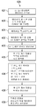
도 1a는 종래의 전계-효과 디바이스를 예시한다.
도 1b는 종래의 전계 효과 디바이스의 온-저항에 대한 저항성 경로를 예시한다.
도 2a는 통합된 부 온도 계수 저항기를 갖는 전계-효과 디바이스의 바람직한 실시예를 예시한다.
도 2b는 통합된 부 온도 계수 저항기를 갖는 전계 효과 디바이스의 바람직한 실시예의 온-저항에 대한 저항성 경로를 예시한다.
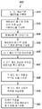
도 3은 종래 기술의 수직 전계 효과 디바이스에 대한 접합 온도에 따른 정규화된 온-저항의 예시적 그래프, 통합된 NTC 저항기를 갖는 수직 전계 효과 디바이스의 바람직한 실시예에 대한 접합 온도에 따른 정규화된 온-저항의 예시적 그래프, 그리고 독립된 부 온도 계수 저항기의 온도 의존성 곡선이다.
도 4a는 온도에 따른 온-저항의 감소된 편차를 갖는 수직 전계 효과 디바이스를 구성하기 위한 방법의 바람직한 실시예의 흐름도이다.
도 4b는 온도에 따른 온-저항의 감소된 편차를 갖는 수직 전계 효과 디바이스를 구성하기 위한 방법의 다른 실시예의 흐름도이다.
도 4c는 온도에 따른 온-저항의 감소된 편차를 갖는 수직 전계 효과 디바이스를 구성하기 위한 방법의 다른 실시예의 흐름도이다.
도 4d는 온도에 따른 온-저항의 감소된 편차를 갖는 수직 전계 효과 디바이스를 구성하기 위한 방법의 다른 실시예의 흐름도이다.
도 4e는 온도에 따른 온-저항의 감소된 편차를 갖는 수직 전계 효과 디바이스를 구성하기 위한 방법의 다른 실시예의 흐름도이다.
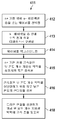
도 4f는 온도에 따른 온-저항의 감소된 편차를 갖는 수직 전계 효과 디바이스를 구성하기 위한 방법의 다른 실시예의 흐름도이다.
도 5는 부 온도 계수 저항기를 구성하기 위한 방법의 바람직한 실시예의 흐름도이다.Figure 1A illustrates a conventional field effect device.
Figure IB illustrates a resistive path to an on-resistance of a conventional field effect device.
2A illustrates a preferred embodiment of a field-effect device having an integrated negative temperature coefficient resistor.
Figure 2B illustrates the resistive path to the on-resistance of a preferred embodiment of a field effect device having an integrated negative temperature coefficient resistor.
Figure 3 is an exemplary graph of normalized on-resistance versus junction temperature for a vertical field effect device of the prior art, a normalized on-resistance versus junction temperature for a preferred embodiment of a vertical field effect device with an integrated NTC resistor, An exemplary graph of the resistance, and a temperature dependent curve of an independent negative temperature coefficient resistor.
4A is a flow diagram of a preferred embodiment of a method for constructing a vertical field effect device having a reduced deviation of on-resistance with temperature.
Figure 4B is a flow diagram of another embodiment of a method for constructing a vertical field effect device having a reduced deviation of on-resistance with temperature.
4C is a flow diagram of another embodiment of a method for constructing a vertical field effect device having a reduced deviation of on-resistance with temperature.
4D is a flow diagram of another embodiment of a method for constructing a vertical field effect device having a reduced deviation of on-resistance with temperature.
Figure 4e is a flow diagram of another embodiment of a method for constructing a vertical field effect device having a reduced deviation of on-resistance with temperature.
Figure 4f is a flow diagram of another embodiment of a method for constructing a vertical field effect device having a reduced deviation of on-resistance with temperature.
Figure 5 is a flow diagram of a preferred embodiment of a method for constructing a negative temperature coefficient resistor.
수직 반도체 디바이스들은 반도체 구조들(예컨대, MOSFET들, IGBT들 및 다이오드들)이며, 여기서 전류 흐름의 주된 방향은 수직 방향인바, 즉 상부로부터 하부로의 방향, 혹은 하부로부터 상부로의 방향, 혹은 이들 방향 모두를 말한다. 개개의 전력 반도체 디바이스들은 종종 이러한 수직 아키텍처로 구축된다.Vertical semiconductor devices are semiconductor structures (e.g., MOSFETs, IGBTs, and diodes), where the primary direction of current flow is a vertical direction, that is, a direction from top to bottom, or from bottom to top, Direction. Individual power semiconductor devices are often built with this vertical architecture.
"온-저항"(RdsOn)은 반도체 디바이스의 전극에 전압 및/또는 전류가 인가됨으로써 "온-상태(on-state)"로 바이어스(bias)될 때의 반도체 디바이스의 저항이다. 예를 들어, MOSFET은 게이트 전극, 소스 전극, 및 드레인 전극을 가지며, 드레인 전극과 소스 전극 간에는 드레인-소스 전압(Vds)이 인가되고, 게이트 전극과 소스 전극 간에는 게이트-소스 전압(Vgs)이 인가된다. "온-상태"는 소스 전극으로부터 드레인 전극으로의 전류(Id)가 게이트-소스 전압에 의해 인에이블(enable)된 것을 의미한다. 예를 들어, 전력 MOSFET에 있어서, RdsOn은 다음과 같이 정의된다.The "on-resistance" RdsOn is the resistance of the semiconductor device when it is biased "on-state" by applying voltage and / or current to the electrodes of the semiconductor device. For example, the MOSFET has a gate electrode, a source electrode, and a drain electrode, a drain-source voltage Vds is applied between the drain electrode and the source electrode, and a gate-source voltage Vgs is applied between the gate electrode and the source electrode. do. The "on-state" means that the current Id from the source electrode to the drain electrode is enabled by the gate-source voltage. For example, for a power MOSFET, RdsOn is defined as:
![]()
![]()
여기서, 드레인-소스 전압(Vds)은 전형적으로 0.1V 내지 5V의 값으로 설정되고, 게이트-소스 전압(Vgs)은 전형적으로 10V로 설정된다.Here, the drain-source voltage Vds is typically set to a value of 0.1V to 5V, and the gate-source voltage Vgs is typically set to 10V.
비-전하 보상 수직 전계 효과 디바이스들(non-charge compensated vertical field effect devices) 및 전하-보상 수직 전계 효과 디바이스들(charge-compensated vertical field effect devices)(예를 들어, 슈퍼-접합 MOSFET들(super-junction MOSFETS))은 일부 다른 수직 반도체 디바이스들과 같이, 정 온도 계수 디바이스들(positive temperature coefficient devices)이다. 일반적으로, 정 온도 계수 디바이스들은 온도 증가에 따라 증가하는 디바이스 저항을 갖는다.Non-charge compensated vertical field effect devices and charge-compensated vertical field effect devices (e.g., super-junction MOSFETs) junction MOSFETS) are positive temperature coefficient devices, like some other vertical semiconductor devices. In general, constant temperature coefficient devices have a device resistance that increases with increasing temperature.
역으로, NTC 디바이스들은 온도 증가에 따라 감소하는 저항을 갖는다. NTC 디바이스의 일 예는 NTC 저항기이다.Conversely, NTC devices have a resistance that decreases with increasing temperature. An example of an NTC device is an NTC resistor.
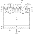
도 1a는 종래 기술에서 알려진 바와 같은 수직 MOSFET 디바이스(100)의 단면도를 보여준다. 수직 전계-효과 디바이스(100)는 상부 표면(121) 및 하부 표면(122)을 구비하고, 소스 전극(102), 드레인 전극(103), 및 게이트 전극(101)을 포함한다. 게이트 전극은 소스 전극(102)과 드레인 전극(103) 간의 전류 흐름을 제어한다. 수직 전계-효과 디바이스(100)는 또한 "n+" 드레인 영역(106)을 포함하며, 드레인 전극(103)의 형성을 위해 하부 표면에 인접하는 금속 층(107)을 갖는다. n+ 드레인 영역(106)은 "n-" 드리프트 영역(drift region)(105)과 접촉한다. n- 드리프트 영역(105)은 또한 "p-" 타입 바디 영역(body region)(140)과 접촉한다.1A shows a cross-sectional view of a
n+ 소스 영역(109)은 "p" 타입 바디 영역들에 인접한다. p 타입 바디 영역들은 p- 바디(140), "p+" 바디(141), 및 p+ 바디-접촉 영역(142)을 포함한다. p+ 바디-접촉 영역(142)은 소스 금속 층(108)에 접촉하고, 소스 금속 층(108)은 n+ 소스 영역, p 타입 바디 영역들, 및 드레인 전극(103) 간에 형성되는 기생 양극성 접합 트랜지스터(parasitic bipolar junction transistor)의 우발적 여기(excitation)를 피하기 위해 n+ 소스 영역(109)을 p+ 바디-접촉 영역(142)에 전기적으로 단락시킨다. 소스 금속 층(108)은 또한 소스 전극(102)과 접촉한다. n- 드리프트 영역(105)은 p-타입 바디 영역들(140, 141, 142) 아래에 있음과 아울러 n+ 드레인 영역(106)에 인접한다.The n +
게이트 영역(113)은 절연 옥사이드 층(insulation oxide layer)(112)과 접촉하고, 절연 옥사이드 층(112)은 n- 드리프트 영역(105), p- 바디 영역(140), n+ 소스 영역(109) 및 절연 층(111)에 인접한다. 게이트 영역(113)은 게이트 물질로 채워지며 게이트 옥사이드 층(112)에 인접한다. 게이트 영역(113)은 게이트 전극(101)과 전기적으로 접촉한다. 게이트 옥사이드 층(112)은 또한 n- 드리프트 영역(105)에 인접한다. MOSFET 디바이스들에서 일반적으로 사용되는 게이트 물질은 다결정성 실리콘(polycrystalline silicon)(폴리실리콘(polysilicon))이다.The
도 1b는 종래 기술의 디바이스의 온-저항에 대한 경로를 보여준다. 방정식 1에서와 같은 온-저항은 디바이스의 온-상태 동안 소스와 드레인 간의 총 저항이다. 온-저항에 대한 경로가 경로(150)에서 보여지고 있다. 수직 전계 효과 디바이스(100)에 있어서, 온-저항은 다음과 같이 일련의 저항 결합으로 주어진다.Figure 1B shows the path to on-resistance of a prior art device. The on-resistance, as in
![]()
![]()
여기서, RdsOn은 온-저항이고, Rn(151)은 n+ 소스 영역(109)의 저항이고, 그리고 Rch(152)는 p-타입 바디 영역(140)의 p- 부분에 형성된 채널의 저항이다. Ra(153)는 인가되는 게이트-소스 전압에 의해 변조되는 n- 드리프트 영역의 표면 저항이다. JFET 영역(130)은 p 타입 바디 (p- 바디) 영역(140)의 표면들(132) 사이에 있는 n- 드리프트 영역(105)의 일부분이다. 드레인 전압이 공급됨에 따라, 공핍 영역이 표면들(132)에서의 접합부로부터 바깥쪽을 향해 확장하고, 이것은 저항(154)(Rj)을 유발 및 증가시키는데 왜냐하면 표면들(132) 사이에 있는 n- 드리프트 영역의 압축(constriction)때문이다. Rj(154)는 JFET 영역의 저항이다. RD(155)는 JFET 영역(130)과 n+ 드레인 영역(106)의 상부 간의 저항이다. RD는 n- 드리프트 영역의 저항이며, 고전압 MOSFET에서 RdsOn의 가장 지배적 인자이다. RS(156)는 n+ 드레인 영역의 저항이다. RS는 또한, 브레이크다운 전압(breakdown voltage)이 약 50V 아래에 있는 저전압 MOSFET에서, 온-저항에 큰 영향을 미친다. 추가적인 온-저항이 다양한 영역들 간의 비-이상적 접촉으로부터 일어날 수 있고, 뿐만 아니라 디바이스를 패키지에 연결하기 위해 사용되는 전극 리드(electrode lead)들로부터 일어날 수 있다.Here, RdsOn is the on-resistance, Rn 151 is the resistance of the n +
RdsOn은 온도에 따라 증가하는데, 왜냐하면 온도가 증가함에 따라 정공들 및 전자들의 이동도가 감소하기 때문이다. n- 채널 전력 MOSFET 디바이스의 RdsOn은 다음과 같은 방정식으로 추정될 수 있다.RdsOn increases with temperature because the mobility of holes and electrons decreases as the temperature increases. The RdsOn of an n-channel power MOSFET device can be estimated by the following equation.
![]()
![]()
여기서, T는 디바이스 온도(단윈: 켈빈(Kelvin))이고, β는 온도 계수이고, RdsOn(T)은 디바이스 온도(T)에서의 온-저항이다. 온도 계수는 양의 값이고 일반적으로 그 범위는 MOSFET 디바이스들에 대해 2.0 내지 2.5이다.Where T is the device temperature (monohydrate: Kelvin), beta is the temperature coefficient and RdsOn (T) is the on-resistance at the device temperature T. The temperature coefficient is a positive value and typically the range is 2.0 to 2.5 for MOSFET devices.
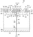
도 2a는 RdsOn 온도 보상을 갖는 수직 전계 효과 디바이스(200)의 바람직한 실시예의 단면도를 보여준다. 상부 표면(221) 및 하부 표면(222)이 제공되며, 소스 전극(202), 드레인 전극(203), 및 게이트 전극(201)이 포함되어 있다. 게이트 전극(201)은 소스 전극(202)과 드레인 전극(203) 간의 전류 흐름을 제어한다. 디바이스(200)는 또한 n+ 드레인 영역(206)을 포함한다. n+ 드레인 영역(206)에 인접하여 저항성 층(220)이 존재한다. 저항성 층(220)은 부 온도 계수를 나타낸다. 저항성 층(220)에 인접하여 금속 층(207)이 존재한다. 금속 층(207)은 드레인 전극(203)에 부착된다. n+ 드레인 영역(206)은 n- 드리프트 영역(205)과 접촉한다. n- 드리프트 영역(205)은 p 타입 바디 영역들(240, 241, 242)과 접촉한다.2A shows a cross-sectional view of a preferred embodiment of a vertical
n+ 소스 영역(209)은 p 타입 바디 영역들에 인접한다. p 타입 바디 영역들은 p- 바디(240), p+ 바디(241), 및 p+ 바디 접촉 영역(242)을 포함한다. p+ 바디-접촉 영역(242)은 소스 금속 층(208)에 접촉하고, 소스 금속 층(208)은 n+ 소스 영역(209)을 p 타입 바디 영역들(240, 241, 242)에 전기적으로 단락시킨다. 소스 전극(202)은 소스 금속 층(208)에 부착된다.The n +
게이트 영역(213)은 게이트 옥사이드 층(212)에 인접하고, 게이트 옥사이드 층(212)은 n- 드리프트 영역(205), p- 바디 영역(240), n+ 소스 영역(209) 및 절연 층(211)에 인접한다. 게이트 영역(213)은 게이트 전극(201)과 전기적으로 접촉한다. 게이트 옥사이드 층(212)은 또한 n- 드리프트 영역(205)에 인접한다.The
도 2b는 바람직한 디바이스 실시예의 온-저항에 대한 경로(250)를 보여준다. 디바이스(200)에 대해, 온-저항은 다음과 같은 방정식으로 주어진다.2B shows a
![]()
![]()
여기서, RdsOn은 온-저항이고, Rn(251)은 n+ 소스 영역(209)의 저항이고, Rch(252)는 p- 바디 영역(240)에 형성된 채널의 저항이다. JFET 영역(230)은 p 타입 바디 (p- 바디) 영역(240)의 표면들(232) 사이에 있는 n- 드리프트 영역(205)의 일부분이다. 드레인 전압이 공급됨에 따라, 공핍 영역이 표면들(232)에서의 접합부로부터 바깥쪽을 향해 확장하고, 이것은 저항(Rj)을 생성 및 증가시키는데 왜냐하면 표면들(232) 사이에 있는 n- 드리프트 영역의 압축때문이다. Rj(254)는 JFET 영역의 저항이다. RD(255)는 JFET 영역(230)과 n+ 드레인 영역(206)의 상부 간의 n- 드리프트 영역 저항이다. Ra(253)는 인가되는 게이트-소스 전압에 의해 변조되는 n- 드리프트 영역의 표면 저항이다. RS(256)는 n+ 드레인 영역의 저항이다. RNTC(257)는 부온도 계수를 갖는 저항성 층(220)의 저항인바, 온도 증가에 따라 RNTC(257)의 저항에서의 감소가 일어나는 특징이 있다.Here, RdsOn the on-resistance and, R n (251) is the resistance of the n + source region (209), R ch (252 ) is a resistance of the channel formed in the p-
수직 MOSFET 디바이스의 바람직한 실시예에서, MOSFET과 직렬로 연결되는 NTC 저항기를 부가함으로써 온도에 따른 RdsOn 저항의 편차 감소가 달성된다.In a preferred embodiment of the vertical MOSFET device, a reduction in the RdsOn resistance variation with temperature is achieved by adding an NTC resistor in series with the MOSFET.
바람직한 실시예에서, NTC 저항기는 저항성 층(220)에 의해 제공되며, 이러한 NTC 저항기는 인-시츄(in-situ)로 도핑되는 폴리실리콘(혹은 예를 들어, 스퍼터링(sputtering)에 의해 증착되는 비정질 실리콘)으로 만들어지는 박막(thin film)으로 구성된다. 또 하나의 다른 실시예에서, 저항성 층(220)은, 주입에 의해 도핑되고 후속적으로 어닐링되는 폴리실리콘(혹은 비정질 실리콘)으로 구성되는 박막이며, 여기서 폴리실리콘 혹은 비정질 실리콘 층의 두께는 대략 100 옹스트롬(angstroms) 내지 대략 4000 옹스트롬의 범위 내에 있다.In a preferred embodiment, an NTC resistor is provided by a
폴리실리콘 혹은 비정질 실리콘 박막의 도핑 레벨은 바람직하게는 약 1e17 atoms/cm3 내지 약 1e21 atoms/cm3의 범위 내에 있다. 이러한 값들은 ± 5%만큼 변할 수 있다. 폴리실리콘 혹은 비정질 실리콘 박막 내의 도펀트(dopant)들은, 베이스 온도(base temperature)(예컨대, 25℃)에서의 저항성 층에 대해 원하는 저항 값, 그리고 저항 값의 원하는 부 온도 계수를 달성하기 위해 요구되는 바에 따라, 비소(arsenic), 인(phosphorus), 붕소(boron) 혹은 이러한 원소들의 임의의 조합으로 구성되는 원소들의 그룹으로부터 선택된다.Doping levels of polysilicon or amorphous silicon thin film is preferably in the range of about 1e17 atoms / cm 3 to about 1e21 atoms / cm 3. These values can vary by +/- 5%. The dopants in the polysilicon or amorphous silicon thin film are doped to a desired resistance value for the resistive layer at a base temperature (e.g., 25 占 폚) And is thus selected from the group of elements consisting of arsenic, phosphorus, boron or any combination of these elements.
또 하나의 다른 실시예에서, 저항성 층(220)은 실리콘-크롬(silicon-chromium)으로 만들어지는 금속화된 저항성 박막이다. 실리콘-크롬 막의 실리콘 퍼센티지는 바람직하게는 약 40% 내지 약 80%의 범위 내에 있다. 이러한 값들은 ± 5%만큼 변할 수 있다. 실리콘-크롬 막의 두께는, 베이스 온도(예컨대, 25℃)에서의 저항성 층에 대해 원하는 시트 저항 값(sheet resistance value), 그리고 저항 값의 원하는 부 온도 계수를 달성하기 위해 요구되는 바에 따라, 대략 25 옹스트롬 내지 대략 2000 옹스트롬의 범위 내에 있다. 이러한 값들은 ± 10%만큼 변할 수 있다.In yet another embodiment, the
또 하나의 다른 실시예에서, 저항성 층(220)은 실리콘-니켈(silicon-nickel)로 만들어지는 금속화된 저항성 박막이다. 실리콘-니켈 막의 실리콘 퍼센티지(silicon percentage)는 바람직하게는 약 40% 내지 약 80%의 범위 내에 있다. 실리콘-니켈 막의 두께는, 베이스 온도(예컨대, 25℃)에서의 저항성 층에 대해 원하는 시트 저항 값, 그리고 저항 값의 원하는 부 온도 계수를 달성하기 위해 요구되는 바에 따라, 대략 25 옹스트롬 내지 대략 2000 옹스트롬의 범위 내에 있다. 이러한 값들은 ± 10%만큼 변할 수 있다.In yet another embodiment, the
도 3은 수직 전계-효과 디바이스 내에 저항성 층(220)을 포함하는 효과의 예를 예시적으로 보여주는 그래프이다. 그래프(300)는 디바이스의 접합 온도에 따른 저항(단위: 오옴)을 도시한 것이다. 그래프(300)는 3개의 곡선을 포함한다. 이들 곡선들은 약 -25℃ 내지 약 150℃ 범위 내에 있는 접합 온도에 대해 도시된 것이다. 곡선(310)은 β=2.0에 대해서 방정식 3을 따르는 온도 의존성을 보여주는 MOSFET 디바이스의 온-저항을 도시한 것이고, 그 온도 의존성은 -25℃에서의 약 0.8 오옴으로부터 150℃에서의 약 2.25 오옴에 이르는 범위를 갖는다. 저항 값들은 ± 5%만큼 변할 수 있다. 곡선(320)은 부 온도 계수 저항성 층의 저항을 도시한 것이다. 저항성 층은 -25℃에서의 약 1.6 오옴으로부터 125℃의 온도 및 그 이상에서의 약 1.0 오옴의 점근값(asymptotic value)에 이르는 범위를 갖는 온도 의존성을 보여준다. 곡선(330)은 MOSFET 디바이스와 직렬로 접촉하고 있는 저항성 층을 갖는 합성 디바이스의 합성 온-저항을 도시한 것이다. 합성 온-저항은 -25℃에서의 약 2.4 오옴으로부터 150℃에서의 약 3.2 오옴에 이르는 범위를 갖는 온도 의존성을 보여주고 있는바, 온도 범위 -25℃에서 150℃에 걸친 총 저항 편차는 0.8 오옴이다. 이러한 예에서, NTC 저항기(220)를 갖는 MOSFET의 합성 저항(RdsOn)은 NTC 저항기가 없는 MOSFET과 비교하여 더 평평하고 안정된 저항 프로파일을 보여주고 있다. 이러한 예에서의 합성 저항은 25℃와 150℃ 간에 약 32%만큼 변했고, 반면 비-합성 MOSFET의 RdsOn은 거의 95%만큼 변했다. 따라서, 합성 디바이스의 온도에 따른 온-저항(RdsOn)의 편차는 저항성 층이 없는 MOSFET 디바이스에 대한 온-저항의 온도 편차와 비교해 약 50%만큼 감소된다.FIG. 3 is a graph illustratively illustrating an example of the effect of including a
도 4a를 참조하면, 전계 효과 디바이스 및 기판의 바람직한 실시예를 구성하는 바람직한 방법(400)이 설명된다. 단계(402)에서, n+ 기판의 상부 상에 n- 에피택셜 층을 갖는 웨이퍼가 반도체 기판으로서 선택된다. 이러한 웨이퍼에서, n- 에피택셜 층은 에피택셜 층 성장 동안 정당한 n- 레벨까지 도핑된다. 단계(404)에서, 수직 전계 효과 디바이스가 n- 에피택셜 층 상에 구성된다. 바람직한 실시예에서, MOSFET은 수직 전계 효과 디바이스이다.4A, a
단계(406)에서는, 웨이퍼 두께를 감소시키기 위해 제 2 면 상에 백그라인드(backgrind)가 행해진다.In
단계(407)에서, NTC 저항성 박막이 n+ 기판 상에 성장 혹은 증착된다. 예를 들어, NTC 저항성 박막은 제 2 면 상에 증착 혹은 성장되는 폴리실리콘으로 만들어질 수 있거나, 또는 스퍼터링 혹은 다른 방법에 의해 증착되는 비정질 실리콘으로 만들어질 수 있다. NTC 저항성 박막은 인-시츄로 도핑될 수 있다.At
단계(408)에서는, NTC 저항성 박막이 인-시츄로 도핑되었는지 여부에 따라 그리고 이러한 도핑이 원하는 부 온도 계수 특성들을 달성하기에 충분한지 여부에 따라, NTC 저항성 박막이 원하는 부 온도 계수의 저항을 갖도록 하기 위해 NTC 저항성 박막은 주입에 의해 더 도핑될 수 있다. 단계(409)에서, NTC 저항성 박막은 (예를 들어, 레이저 어닐링 혹은 RF 어닐링에 의해) 어닐링된다.In
단계(410)에서는, 드레인 연결을 생성하기 위해 NTC 저항성 박막에 금속 층이 도포된다.In
도 4b를 참조하면, 전계 효과 디바이스 및 기판의 바람직한 실시예를 구성하는 다른 방법(411)이 설명된다. 단계(412)에서, n+ 기판의 상부 상에 n- 에피택셜 층을 갖는 웨이퍼가 반도체 기판으로서 선택된다. 단계(413)에서, 수직 전계 효과 디바이스가 n- 에피택셜 층 상에 구성된다. 바람직한 실시예에서, MOSFET은 수직 전계 효과 디바이스이다. 단계(414)에서는, 제 2 면 상에 백그라인드가 행해진다. 단계(415)에서는, NTC 저항성 박막이 n+ 기판 상에서 성장 혹은 증착된다. NTC 저항성 박막은 원하는 부 온도 계수를 달성하기 위해 인-시츄로 도핑되는 실리콘-니켈 혹은 실리콘-크롬으로부터 만들어지는 금속화된 저항성 박막이다. 단계(416)에서는, 금속화된 NTC 저항성 박막에 대해, 금속화된 박막의 어닐링을 위해 저온 신터링(low temp sintering)이 행해질 수 있다. 단계(418)에서는, 드레인 연결을 생성하기 위해 NTC 저항성 박막에 금속 층이 도포된다.4B, another
도 4c를 참조하여, 수직 전계 효과 디바이스를 구성하는 다른 방법(425)이 설명될 것이다. 단계(427)에서, 기판에 대해 n- 논-에피택셜 웨이퍼(non-epitaxial wafer)가 선택된다.Referring to Figure 4C, another
단계(429)에서, 수직 전계 효과 디바이스가 제 1 면 상에 구성된다. 단계(431)에서, 제 2 면 상에 백그라인드가 행해진다. 단계(432)에서, n+ 드레인 영역이 제 2 면 상에 주입된다. 단계(433)에서, n+ 드레인 영역이 어닐링된다. 단계(435)에서, NTC 저항성 박막이 제 2 면 상에 성장 혹은 증착되며, 여기서 저항성 막은 인-시츄로 도핑될 수 있다. 단계(436)에서는, NTC 저항성 박막이 인-시츄로 도핑되었는지 여부에 따라 그리고 이러한 도핑이 원하는 부 온도 계수 특성들을 달성하기에 충분한지 여부에 따라, NTC 저항성 막이 주입에 의해 더 도핑될 수 있다. 단계(438)에서는, NTC 저항성 박막이 어닐링된다. 단계(439)에서는, 드레인 연결을 생성하기 위해 제 2 면이 금속화된다.In
도 4d를 참조하면, 수직 전계 효과 디바이스를 구성하는 다른 방법(440)이 설명된다. 단계(441)에서, 기판에 대해 n- 논-에피택셜 웨이퍼가 선택된다.Referring to Figure 4d, another
단계(443)에서, 수직 전계 효과 디바이스가 제 1 면 상에 구성된다. 단계(444)에서, 제 2 면 상에 백그라인드가 행해진다.At
단계(445)에서, n+ 드레인 영역이 제 2 면 상에 주입된다. 단계(446)에서, n+ 드레인 영역이 어닐링된다. 단계(447)에서, NTC 저항성 박막이 제 2 면 상에 성장 혹은 증착된다. 단계(448)에서는, 원하는 부 온도 계수 특성을 달성하기 위해 NTC 저항성 박막이 주입을 통해 도핑된다. 단계(449)에서는, NTC 저항성 박막이 어닐링된다. 단계(450)에서는, 드레인 연결을 생성하기 위해 제 2 면이 금속화된다.At
도 4e를 참조하여, 수직 전계 효과 디바이스를 구성하는 다른 방법(451)이 설명될 것이다. 단계(452)에서, 기판에 대해 n- 논-에피택셜 웨이퍼가 선택된다.Referring to Figure 4E, another
단계(456)에서, 수직 전계 효과 디바이스가 제 1 면 상에 구성된다. 단계(457)에서, 제 2 면 상에 백그라인드가 행해진다. 단계(458)에서, n+ 드레인 영역이 제 2 면 상에 주입된다. 단계(460)에서, NTC 저항성 박막이 제 2 면 상에 성장 혹은 증착되며, 여기서 박막은 인-시츄로 도핑될 수 있다. 단계(461)에서는, 저항성 박막이 인-시츄로 도핑되는지 여부에 따라 그리고 이러한 도핑이 원하는 부 온도 계수 특성을 달성하기에 충분한지 여부에 따라, NTC 저항성 막이 주입에 의해 더 도핑될 수 있다. 단계(462)에서는, n+ 드레인 영역과 NTC 저항성 박막이 함께 어닐링된다. 단계(464)에서는, 드레인 연결을 생성하기 위해 제 2 면이 금속화된다.In
도 4f를 참조하여, 수직 전계 효과 디바이스를 구성하는 다른 방법(475)이 설명될 것이다. 단계(477)에서, 기판에 대해 n- 논-에피택셜 웨이퍼가 선택된다. 단계(481)에서, 수직 전계 효과 디바이스가 제 1 면 상에 구성된다. 단계(482)에서, 백그라인드가 행해진다.Referring to FIG. 4F, another
단계(483)에서, 폴리실리콘 혹은 비정질 실리콘 NTC 저항성 막이 n- 기판 상에 성장 혹은 증착된다. 단계(485)에서, n+ 드레인 영역이 NTC 막을 통해 주입된다. NTC 막을 통해 n+ 드레인 영역을 주입하는 것에 대한 한 가지 이점은 NTC 막의 유효 깊이가 n+ 드레인 주입의 깊이에 의해 설정될 것이라는 점이다. 이것은 결과적으로 n+ 이온 주입의 정밀한 깊이 제어가 가능하기 때문에 웨이퍼에 걸쳐 유효 NTC 막 두께를 매우 균일하게 할 것이다. 단계(486)에서는, NTC 막이 인-시츄로 도핑되는지 여부에 따라 그리고 이러한 도핑이 원하는 부 온도 계수 특성을 달성하기에 충분한지 여부에 따라, NTC 저항성 막이 주입에 의해 더 도핑될 수 있다. 단계(487)에서는, NTC 드레인 영역과 NTC 막이 함께 어닐링된다. 단계(439)에서는, 드레인 연결을 생성하기 위해 제 2 면이 금속화된다.In
도 5를 참조하면, 저항성 박막을 선택 및 형성하는 방법(520)이 설명된다. 단계(522)에서는, 합성 디바이스에 대한 합성 온-저항이, 온도에 따른 온-저항의 원하는 편차와 함께 특정된다. 단계(524)에서, 일 세트의 디바이스들에 대해 접합 온도의 범위에 걸쳐 일 세트의 온-저항 값들이 측정되고 디바이스 온-저항을 결정하기 위해 평균화된다. 단계(526)에서는, 특정된 합성 온-저항으로부터 디바이스 온-저항을 뺌으로써 저항성 박막의 온도 의존성 곡선이 결정된다.Referring to FIG. 5, a
단계(528)에서는, 온도 의존성 곡선에 근거하여, 아울러 온도 팽창 계수를 포함하는 반도체 기판과의 물리적 호환가능성에 근거하여, 저항성 박막에 대한 물질이 선택되고 또한 특정된다. 이러한 물질은 특정 도핑 레벨을 갖는 도펀트들을 포함할 수 있다. 단계(530)에서는, 이러한 물질에 대해 저항성 박막에 대한 시트 저항이 결정된다.At
단계(532)에서는, 저항성 박막을 생성하기 위해 일 세트의 원하는 프로세싱 특성들이 결정된다. 일 세트의 원하는 프로세싱 특성들은, 저항성 박막의 원하는 성분, 도핑 타입 및 레벨, 그리고 두께를 포함하고, 이것은 25℃에서의 특정된 저항을 시트 저항으로 나눔으로써 결정된다. 단계(533)에서, 수직 전계 디바이스가 웨이퍼의 제 1 면 상에 구성된다.In
단계(534)에서는, 물질 특성, 프로세싱 특성 및 원하는 성분, 도핑 타입 및 레벨, 그리고 웨이퍼의 면 상의 두께에 따라 저항성 박막이 성장 혹은 증착되고 프로세싱된다.At
단계(536)에서, 박막은 인-시츄로 혹은 주입에 의해 도핑된다. 단계(538)에서, 박막은 (어닐링이 요구된다면) 어닐링된다.In
본 방법의 바람직한 실시예에서, 저항성 박막의 물질은 폴리실리콘, 비정질 실리콘, 실리콘-크롬, 실리콘-니켈 혹은 이들 물질의 임의의 조합을 포함하는 물질들의 그룹으로부터 선택된다. 또 하나의 다른 실시예에서는, 부 온도 계수의 저항을 달성하기 위한 물질 및 프로세싱 특성들이 도출될 수 있다면 상이한 물질이 선택될 수 있다.In a preferred embodiment of the method, the material of the resistive thin film is selected from the group of materials comprising polysilicon, amorphous silicon, silicon-chromium, silicon-nickel or any combination of these materials. In yet another embodiment, different materials may be selected provided that the materials and processing characteristics for achieving the resistance of the sub-temperature coefficient can be derived.
제 1 실시예에서는, 폴리실리콘 혹은 비정질 실리콘이 저항성 박막에 대한 물질로서 선택되고, 폴리실리콘은 인-시츄로 도핑된다. 제 2 바람직한 실시예에서는, 폴리실리콘 혹은 비정질 실리콘이 저항성 박막에 대한 물질로서 선택되고, 폴리실리콘 혹은 비정질 실리콘은 주입에 의해 도핑되고 후속적으로 어닐링된다. 제 1 실시예 및 제 2 실시예에서, 폴리실리콘 혹은 비정질 실리콘 박막의 도핑 레벨은 1e17 atoms/cm3 내지 1e21 atoms/cm3의 범위 내에 있도록 선택되고, 폴리실리콘 혹은 비정질 실리콘 박막 내의 도펀트들은 베이스 온도(25℃)에서의 저항성 층에 대해 원하는 저항 값, 그리고 원하는 온도 의존성 곡선을 달성하기 위해 요구되는 바에 따라, 비소, 인, 붕소 혹은 이러한 원소들의 임의의 조합으로 구성되는 원소들의 그룹으로부터 선택된다.In the first embodiment, polysilicon or amorphous silicon is selected as the material for the resistive thin film, and the polysilicon is doped in-situ. In a second preferred embodiment, polysilicon or amorphous silicon is selected as the material for the resistive thin film, and polysilicon or amorphous silicon is doped by implantation and subsequently annealed. The first embodiment and the second embodiment, the polysilicon or the doping level of the amorphous silicon thin film is selected to be in the range of 1e17 atoms / cm 3 to 1e21 atoms / cm 3, a polysilicon or the dopant in the amorphous silicon thin film are a base temperature Phosphorus, boron, or any combination of these elements, as required to achieve a desired resistance value for the resistive layer at room temperature (25 占 폚) and a desired temperature dependency curve.
제 3 실시예에서는, 실리콘-크롬이 저항성 박막의 물질로서 선택된다. 실리콘-크롬 막의 실리콘 퍼센티지는 40% 내지 80%의 범위 내에서 선택되고, 이러한 박막은 베이스 온도(예를 들어, 25℃)에서의 저항성 층에 대해 원하는 시트 저항 값, 그리고 원하는 온도 의존성 곡선을 달성하기 위해 요구되는 바에 따라, 대략 25A 내지 대략 2000A의 범위 내에 있는 두께로 성장된다.In the third embodiment, silicon-chromium is selected as the material of the resistive thin film. The silicon percentage of the silicon-chromium film is selected in the range of 40% to 80%, and this film has a desired sheet resistance value for the resistive layer at the base temperature (e.g., 25 占 폚) Lt; RTI ID = 0.0 > 2000A. ≪ / RTI >
제 4 실시예에서는, 실리콘-니켈이 저항성 박막의 물질로서 선택된다. 실리콘-니켈 막의 실리콘 퍼센티지는 40% 내지 80%의 범위 내에서 선택되고, 이러한 박막은 베이스 온도(예를 들어, 25℃)에서의 저항성 층에 대해 특정 저항 값, 그리고 원하는 온도 의존성 곡선을 달성하기 위해 요구되는 바에 따라, 대략 25A 내지 대략 2000A의 범위 내에 있는 두께로 성장된다.In the fourth embodiment, silicon-nickel is selected as the material of the resistive thin film. The silicon percentage of the silicon-nickel film is selected within the range of 40% to 80%, and this thin film has a specific resistance value for the resistive layer at the base temperature (e.g., 25 占 폚) Lt; RTI ID = 0.0 > 2000A, < / RTI >
본 개시내용에서 제시되는 실시예들은 본 발명의 구현가능한 예들을 제공하기 위해 의도된 것이지, 본 발명을 한정하려고 의도된 것이 아니다. 예를 들어, Si 이외에 다른 물질들이 베이스 반도체 물질로서 사용될 수 있다. n+ 영역들, n-컬럼들, p-컬럼들 및 p-타입 바디에 대한 도핑 레벨의 다양한 범위가 필요에 따라 사용될 수 있다.The embodiments presented in this disclosure are intended to provide implementable examples of the invention and are not intended to limit the invention. For example, other materials than Si can be used as the base semiconductor material. Various ranges of doping levels for n + regions, n-columns, p-columns and p-type bodies can be used as needed.
Claims (37)
기판(substrate)과;
상기 기판 상에 구성되며 드레인 영역(drain region)을 갖는 수직 전계 효과 디바이스(vertical field effect device)와; 그리고
상기 드레인 영역에 인접하는 부 온도 계수 저항기(negative temperature coefficient resistor)를 포함하는 것을 특징으로 하는 반도체 디바이스.As a semiconductor device,
A substrate;
A vertical field effect device configured on the substrate and having a drain region; And
And a negative temperature coefficient resistor adjacent said drain region.
상기 부 온도 계수 저항기는 폴리실리콘(polysilicon)인 것을 특징으로 하는 반도체 디바이스.The method according to claim 1,
Wherein the sub-temperature coefficient resistor is a polysilicon.
상기 폴리실리콘은 입방 센티미터(cubic centimeter) 당 약 1×10¹⁷개의 원자들 내지 약 1×10²¹개의 원자들로 도핑(doping)되는 것을 특징으로 하는 반도체 디바이스.3. The method of claim 2,
Wherein the polysilicon is doped with about 1 x 10 17 atoms to about 1 x 10 21 atoms per cubic centimeter.
상기 폴리실리콘은 비소(arsenic), 인(phosphorous), 및 붕소(boron)로 이루어진 그룹 중 하나로 도핑되는 것을 특징으로 하는 반도체 디바이스.3. The method of claim 2,
Wherein the polysilicon is doped with one of the group consisting of arsenic, phosphorous, and boron.
상기 부 온도 계수 저항기는 비정질 실리콘(amorphous silicon)인 것을 특징으로 하는 반도체 디바이스.The method according to claim 1,
Wherein the sub-temperature coefficient resistor is amorphous silicon.
상기 비정질 실리콘은 입방 센티미터 당 약 1×10¹⁷개의 원자들 내지 약 1×10²¹개의 원자들로 도핑되는 것을 특징으로 하는 반도체 디바이스.6. The method of claim 5,
Wherein the amorphous silicon is doped with about 1 x 10 17 atoms to about 1 x 10 21 atoms per cubic centimeter.
상기 비정질 실리콘은 비소, 인, 및 붕소로 이루어진 그룹 중 하나로 도핑되는 것을 특징으로 하는 반도체 디바이스.6. The method of claim 5,
Wherein the amorphous silicon is doped with one of the group consisting of arsenic, phosphorus, and boron.
상기 부 온도 계수 저항기는 실리콘-크롬(silicon-chromium)인 것을 특징으로 하는 반도체 디바이스.The method according to claim 1,
Wherein the sub-temperature coefficient resistor is silicon-chromium.
상기 실리콘-크롬은 약 40% 내지 약 80%의 실리콘인 것을 특징으로 하는 반도체 디바이스.9. The method of claim 8,
Wherein the silicon-chromium is about 40% to about 80% silicon.
상기 부 온도 계수 저항기는 실리콘-니켈(silicon-nickel)인 것을 특징으로 하는 반도체 디바이스.The method according to claim 1,
Wherein the sub-temperature coefficient resistor is silicon-nickel.
상기 실리콘-니켈은 약 40% 내지 약 80%의 실리콘인 것을 특징으로 하는 반도체 디바이스.11. The method of claim 10,
Wherein the silicon-nickel is about 40% to about 80% silicon.
상기 부 온도 계수 저항기의 두께는 약 25 옹스트롬(angstroms) 내지 약 2000 옹스트롬인 것을 특징으로 하는 반도체 디바이스.The method according to claim 1,
Wherein the thickness of the sub-temperature coefficient resistor is between about 25 angstroms and about 2000 angstroms.
상기 수직 전계 효과 디바이스는 MOSFET(Metal Oxide Silicon Field Effect transistor)인 것을 특징으로 하는 반도체 디바이스.The method according to claim 1,
Wherein the vertical field effect device is a metal oxide silicon field effect transistor (MOSFET).
상기 수직 전계 효과 디바이스는 전하 보상 MOSFET(charge compensated MOSFET)인 것을 특징으로 하는 반도체 디바이스.The method according to claim 1,
Wherein the vertical field effect device is a charge compensated MOSFET.
상기 MOSFET은 n+ 소스 영역(source region), p- 채널(channel), JFET(Junction Field Effcet Transistor) 영역, n- 드리프트 영역(drift region) 및 부 온도 계수 저항 층(negative temperature coefficient resistance layer)을 구비하며, 상기 MOSFET의 온-저항(on-resistance)은 아래의 방정식에 의해 정의되고,
여기서,
RdsOn = 상기 MOSFET의 온-저항,
Rn = 상기 n+ 소스 영역의 저항,
Rch = 상기 p- 채널의 저항,
Ra = 상기 n- 드리프트 영역의 표면 저항(surface resistance),
Rj = 상기 JFET 영역의 저항,
Rd = 상기 n- 드리프트 영역의 저항,
Rs = 상기 n+ 드레인 영역의 저항, 그리고
RNTC = 상기 부 온도 계수 저항 층의 저항인 것을 특징으로 하는 MOSFET.As MOSFET (Metal Oxide Silicon Field Effect Transistor)
The MOSFET includes an n + source region, a p-channel, a junction field effect transistor (JFET) region, an n-drift region, and a negative temperature coefficient resistance layer And the on-resistance of the MOSFET is defined by the following equation,
here,
RdsOn = on-resistance of the MOSFET,
R n = resistance of the n + source region,
R ch = resistance of said p-channel,
R a = surface resistance of the n-drift region,
R j = resistance of the JFET region,
R d = resistance of the n-drift region,
R s = resistance of the n + drain region, and
R NTC = resistance of said sub-temperature coefficient resistor layer.
상기 RNTC의 범위는 약 -25℃ 내지 약 125℃에서 약 1.6 오옴(ohms) 내지 약 1.0 오옴인 것을 특징으로 하는 MOSFET.16. The method of claim 15,
Wherein the R NTC ranges from about 1.6 ohms to about 1.0 ohms at about -25 ° C to about 125 ° C.
상기 RdsOn의 범위는 약 -25℃ 내지 약 125℃에서 약 2.4 오옴 내지 약 3.2 오옴인 것을 특징으로 하는 MOSFET.16. The method of claim 15,
Wherein the RdsOn ranges from about 2.4 ohms to about 3.2 ohms at about -25 [deg.] C to about 125 [deg.] C.
상기 RdsOn은 약 125℃의 온도 편차에 대해 약 0.8 오옴의 총 저항 편차를 나타내는 것을 특징으로 하는 MOSFET.16. The method of claim 15,
Wherein the RdsOn exhibits a total resistance deviation of about 0.8 Ohms for a temperature deviation of about 125 < 0 > C.
정 온도 계수 디바이스(positive temperature coefficient device)와; 그리고
상기 정 온도 계수 디바이스와 물리적으로 접촉하며 직렬로 연결된 부 온도 계수 저항기를 포함하는 것을 특징으로 하는 수직 전계 효과 디바이스.1. A vertical field effect device,
A positive temperature coefficient device; And
And a negative temperature coefficient resistor in physical contact with and in series with said constant temperature coefficient device.
상기 정 온도 계수 디바이스는 MOSFET인 것을 특징으로 하는 수직 전계 효과 디바이스.20. The method of claim 19,
Wherein the static temperature coefficient device is a MOSFET.
상기 부 온도 계수 저항기는 비정질 실리콘인 것을 특징으로 하는 수직 전계 효과 디바이스.20. The method of claim 19,
Wherein the sub-temperature coefficient resistor is amorphous silicon.
상기 부 온도 계수 저항기는 실리콘-크롬인 것을 특징으로 하는 수직 전계 효과 디바이스.20. The method of claim 19,
Wherein the sub-temperature coefficient resistor is silicon-chrome.
상기 부 온도 계수 저항기는 실리콘-니켈인 것을 특징으로 하는 수직 전계 효과 디바이스.20. The method of claim 19,
Wherein the sub-temperature coefficient resistor is silicon-nickel.
상기 n- 에피택셜 층 상에 수직 전계 효과 디바이스를 구성하는 단계와;
상기 n+ 기판 상에 부 온도 계수 저항성 층을 도포(applying)하는 단계와;
상기 부 온도 계수 저항성 층을 도핑하는 단계와;
상기 부 온도 계수 저항성 층에 금속 층을 도포하는 단계를 포함하는 것을 특징으로 하는 반도체 디바이스를 제조하는 방법.A method of fabricating a semiconductor device on a wafer having an n-epitaxial layer on an n + substrate,
Forming a vertical field effect device on the n-epitaxial layer;
Applying a negative temperature coefficient resistive layer on the n + substrate;
Doping the sub-temperature coefficient resistive layer;
And applying a metal layer to the sub-temperature coefficient resistive layer.
상기 구성하는 단계는 또한 MOSFET를 구성하는 것을 포함하는 것을 특징으로 하는 반도체 디바이스를 제조하는 방법.26. The method of claim 25,
Wherein the configuring step further comprises configuring a MOSFET. ≪ RTI ID = 0.0 > 11. < / RTI >
상기 n- 에피택셜 층 상에 수직 전계 효과 디바이스를 구성하는 단계와;
상기 n+ 기판 상에 부 온도 계수 저항성 층을 도포하는 단계와;
상기 부 온도 계수 저항성 층을 어닐링(annealing)하는 단계와; 그리고
상기 부 온도 계수 저항성 층에 금속 층을 도포하는 단계를 포함하는 것을 특징으로 하는 반도체 디바이스를 제조하는 방법.A method of fabricating a semiconductor device on a wafer having an n-epitaxial layer on an n + substrate,
Forming a vertical field effect device on the n-epitaxial layer;
Applying a negative temperature coefficient resistive layer on the n + substrate;
Annealing the sub-temperature coefficient resistive layer; And
And applying a metal layer to the sub-temperature coefficient resistive layer.
상기 구성하는 단계는 또한 MOSFET를 구성하는 것을 포함하는 것을 특징으로 하는 반도체 디바이스를 제조하는 방법.28. The method of claim 27,
Wherein the configuring step further comprises configuring a MOSFET. ≪ RTI ID = 0.0 > 11. < / RTI >
상기 웨이퍼의 제 1 면 상에 수직 전계 효과 디바이스를 구성하는 단계와;
상기 웨이퍼의 제 2 면에 n+ 영역을 주입하는 단계와;
상기 n+ 영역을 어닐링하는 단계와;
상기 n+ 영역 상에 부 온도 계수 저항성 막을 도포하는 단계와;
상기 부 온도 계수 저항성 막을 주입 도핑(implant doping)하는 단계와;
상기 부 온도 계수 저항성 막을 어닐링하는 단계와; 그리고
상기 제 2 면을 금속화하는 단계를 포함하는 것을 특징으로 하는 반도체 디바이스를 제조하는 방법.A method of fabricating a semiconductor device on a non-epitaxial wafer,
Configuring a vertical field effect device on a first side of the wafer;
Implanting an n + region on a second side of the wafer;
Annealing the n + region;
Applying a negative temperature coefficient resistive film over the n + region;
Implanting the negative temperature coefficient resistive film;
Annealing the negative temperature coefficient resistive film; And
And metallizing said second surface. ≪ RTI ID = 0.0 > 11. < / RTI >
상기 어닐링하는 단계는 또한 레이저 어닐링(laser annealing)을 포함하는 것을 특징으로 하는 반도체 디바이스를 제조하는 방법.30. The method of claim 29,
Wherein the annealing further comprises laser annealing. ≪ RTI ID = 0.0 > 8. < / RTI >
상기 웨이퍼의 제 1 면 상에 수직 전계 효과 디바이스를 구성하는 단계와;
상기 웨이퍼의 제 2 면에 n+ 영역을 주입하는 단계와;
상기 n+ 영역을 어닐링하는 단계와;
상기 n+ 영역 상에 부 온도 계수 저항성 막을 도포하는 단계와;
상기 부 온도 계수 저항성 막을 주입 도핑하는 단계와;
상기 부 온도 계수 저항성 막을 어닐링하는 단계와; 그리고
상기 제 2 면을 금속화하는 단계를 포함하는 것을 특징으로 하는 반도체 디바이스를 제조하는 방법.A method of fabricating a semiconductor device on an n-non-epitaxial wafer,
Configuring a vertical field effect device on a first side of the wafer;
Implanting an n + region on a second side of the wafer;
Annealing the n + region;
Applying a negative temperature coefficient resistive film over the n + region;
Implanting the negative temperature coefficient resistive film;
Annealing the negative temperature coefficient resistive film; And
And metallizing said second surface. ≪ RTI ID = 0.0 > 11. < / RTI >
상기 웨이퍼의 제 1 면 상에 수직 전계 효과 디바이스를 구성하는 단계와;
상기 웨이퍼의 제 2 면에 n+ 드레인 영역을 주입하는 단계와;
상기 제 2 면 상에 부 온도 계수 저항성 막을 도포하는 단계와;
상기 n+ 드레인 영역 및 상기 부 온도 계수 저항성 막을 어닐링하는 단계와; 그리고
상기 제 2 면을 금속화하는 단계를 포함하는 것을 특징으로 하는 반도체 디바이스를 제조하는 방법.A method of fabricating a semiconductor device on an n-non-epitaxial wafer,
Configuring a vertical field effect device on a first side of the wafer;
Implanting an n + drain region on a second side of the wafer;
Applying a negative temperature coefficient resistive film on the second side;
Annealing the n + drain region and the negative temperature coefficient resistive film; And
And metallizing said second surface. ≪ RTI ID = 0.0 > 11. < / RTI >
상기 부 온도 계수 저항성 막을 도포한 이후에, 상기 부 온도 계수 저항성 막을 주입 도핑하는 것을 특징으로 하는 반도체 디바이스를 제조하는 방법.33. The method of claim 32,
Wherein after the application of the sub-temperature coefficient resistive film, the sub-temperature coefficient resistive film is implanted.
상기 웨이퍼의 제 1 면 상에 수직 전계 효과 디바이스를 구성하는 단계와;
상기 웨이퍼의 제 2 면 상에 폴리실리콘 부 온도 계수 저항성 막을 도포하는 단계와;
상기 부 온도 계수 저항성 막을 통해 n+ 영역을 주입하는 단계와;
상기 n+ 영역과 상기 부 온도 계수 저항성 막을 동시에 어닐링하는 단계와; 그리고
상기 부 온도 계수 저항성 막을 금속화하는 단계를 포함하는 것을 특징으로 하는 반도체 디바이스를 제조하는 방법.A method of fabricating a semiconductor device on an n-non-epitaxial wafer,
Configuring a vertical field effect device on a first side of the wafer;
Applying a polysilicon portion temperature coefficient resistive film on a second side of the wafer;
Implanting the n + region through the negative temperature coefficient resistive film;
Annealing the n + region and the sub-temperature coefficient resistive film simultaneously; And
And metallizing said sub-temperature coefficient resistive film. ≪ Desc / Clms Page number 20 >
상기 n+ 영역을 주입한 이후에, 상기 부 온도 계수 저항성 막을 주입 도핑하는 단계를 더 포함하는 것을 특징으로 하는 반도체 디바이스를 제조하는 방법.35. The method of claim 34,
Implanting the negative temperature coefficient resistive film after implanting the n + region. ≪ RTI ID = 0.0 > 11. < / RTI >
상기 반도체 디바이스에 대한 합성 온-저항(composite on-resistance)을 특정하는 단계와;
상기 반도체 디바이스에 대한 요구된 온-저항 편차(on-resistance variation)를 특정하는 단계와;
일 세트의 비-합성 반도체 디바이스들(non-composite semiconductor devices)에 대한 평균 디바이스 온-저항(average device on-resistance)을 결정하는 단계와;
저항성 박막(resistive thin film)에 대한 온도 의존성 곡선(temperature dependence curve)을 결정하는 단계와;
상기 온도 의존성 곡선에 근거하여 임의의 물질을 선택하는 단계와;
상기 물질에 대한 시트 저항(sheet resistive)을 결정하는 단계와;
상기 저항성 박막에 대한 일 세트의 원하는 특성(property)들을 결정하는 단계와;
웨이퍼의 제 1 면 상에 수직 전계 효과 디바이스를 구성하는 단계와;
상기 웨이퍼의 제 2 면에 상기 저항성 박막을 도포하는 단계와; 그리고
상기 저항성 박막을 도핑하는 단계를 포함하는 것을 특징으로 하는 반도체 디바이스를 제조하는 방법.A method of manufacturing a semiconductor device,
Identifying a composite on-resistance for the semiconductor device;
Identifying a desired on-resistance variation for the semiconductor device;
Determining an average device on-resistance for a set of non-composite semiconductor devices;
Determining a temperature dependence curve for a resistive thin film;
Selecting an arbitrary material based on the temperature dependency curve;
Determining a sheet resistive for the material;
Determining a set of desired properties for the resistive film;
Constructing a vertical field effect device on a first side of the wafer;
Applying the resistive thin film to a second side of the wafer; And
And doping the resistive thin film. ≪ Desc / Clms Page number 22 >
상기 저항성 박막을 어닐링하는 단계를 더 포함하는 것을 특징으로 하는 반도체 디바이스를 제조하는 방법.37. The method of claim 36,
And annealing the resistive thin film. ≪ RTI ID = 0.0 > 11. < / RTI >
Applications Claiming Priority (3)
| Application Number | Priority Date | Filing Date | Title |
|---|---|---|---|
| US201361778698P | 2013-03-13 | 2013-03-13 | |
| US61/778,698 | 2013-03-13 | ||
| PCT/US2014/026668 WO2014160453A2 (en) | 2013-03-13 | 2014-03-13 | Device architecture and method for temperature compensation of vertical field effect devices |
Publications (1)
| Publication Number | Publication Date |
|---|---|
| KR20150131195A true KR20150131195A (en) | 2015-11-24 |
Family
ID=51523591
Family Applications (1)
| Application Number | Title | Priority Date | Filing Date |
|---|---|---|---|
| KR1020157028652A KR20150131195A (en) | 2013-03-13 | 2014-03-13 | Device architecture and method for temperature compensation of vertical field effect devices |
Country Status (6)
| Country | Link |
|---|---|
| US (1) | US20140264343A1 (en) |
| EP (1) | EP2973720A4 (en) |
| JP (1) | JP2016516303A (en) |
| KR (1) | KR20150131195A (en) |
| CN (1) | CN105393362A (en) |
| WO (1) | WO2014160453A2 (en) |
Cited By (1)
| Publication number | Priority date | Publication date | Assignee | Title |
|---|---|---|---|---|
| WO2023081586A1 (en) * | 2021-11-02 | 2023-05-11 | Analog Power Conversion LLC | Semiconductor device with improved temperature uniformity |
Families Citing this family (8)
| Publication number | Priority date | Publication date | Assignee | Title |
|---|---|---|---|---|
| DE102014115314B4 (en) * | 2014-10-21 | 2018-10-11 | Infineon Technologies Austria Ag | BIPOLAR TRANSISTOR WITH INSULATED GATE WITH A THERMISTOR WITH NEGATIVE TEMPERATURE COEFFICIENT AND METHOD OF MANUFACTURE |
| DE102015112919B4 (en) * | 2015-08-06 | 2019-12-24 | Infineon Technologies Ag | Semiconductor components, a semiconductor diode and a method for forming a semiconductor component |
| EP3357084A4 (en) | 2015-10-01 | 2019-06-19 | D3 Semiconductor LLC | Source-gate region architecture in a vertical power semiconductor device |
| US9806186B2 (en) | 2015-10-02 | 2017-10-31 | D3 Semiconductor LLC | Termination region architecture for vertical power transistors |
| DE102016104256B3 (en) * | 2016-03-09 | 2017-07-06 | Infineon Technologies Ag | Wide band gap semiconductor device having transistor cells and compensation structure |
| CN113035950B (en) * | 2019-12-25 | 2022-08-05 | 株洲中车时代半导体有限公司 | IGBT chip and preparation method thereof |
| US11869762B2 (en) | 2020-10-13 | 2024-01-09 | Alpha Power Solutions Limited | Semiconductor device with temperature sensing component |
| CN115976482B (en) * | 2022-12-08 | 2024-07-23 | 中国科学院新疆理化技术研究所 | Preparation method of NTC composite thermosensitive film based on ion implantation |
Family Cites Families (19)
| Publication number | Priority date | Publication date | Assignee | Title |
|---|---|---|---|---|
| US3477935A (en) * | 1966-06-07 | 1969-11-11 | Union Carbide Corp | Method of forming thin film resistors by cathodic sputtering |
| US4837606A (en) * | 1984-02-22 | 1989-06-06 | General Electric Company | Vertical MOSFET with reduced bipolar effects |
| JP3030337B2 (en) * | 1991-09-26 | 2000-04-10 | アンリツ株式会社 | Cryogenic thermometer |
| US5304918A (en) * | 1992-01-22 | 1994-04-19 | Samsung Semiconductor, Inc. | Reference circuit for high speed integrated circuits |
| JP3054937B2 (en) * | 1996-03-25 | 2000-06-19 | セイコーインスツルメンツ株式会社 | Semiconductor device and manufacturing method thereof |
| US6627949B2 (en) * | 2000-06-02 | 2003-09-30 | General Semiconductor, Inc. | High voltage power MOSFET having low on-resistance |
| DE10053957C2 (en) * | 2000-10-31 | 2002-10-31 | Infineon Technologies Ag | Temperature compensated semiconductor resistance and its use |
| US7956672B2 (en) * | 2004-03-30 | 2011-06-07 | Ricoh Company, Ltd. | Reference voltage generating circuit |
| JP4064436B2 (en) * | 2004-06-11 | 2008-03-19 | 松下電器産業株式会社 | Power element |
| DE102005061263B4 (en) * | 2005-12-20 | 2007-10-11 | Infineon Technologies Austria Ag | Semiconductor wafer substrate for power semiconductor devices and method of making the same |
| JP5225546B2 (en) * | 2005-12-27 | 2013-07-03 | 株式会社豊田中央研究所 | Semiconductor device |
| US7397691B2 (en) * | 2006-04-24 | 2008-07-08 | International Business Machines Corporation | Static random access memory cell with improved stability |
| JP4483900B2 (en) * | 2007-06-21 | 2010-06-16 | 株式会社デンソー | Method for manufacturing silicon carbide semiconductor device |
| JP5588670B2 (en) * | 2008-12-25 | 2014-09-10 | ローム株式会社 | Semiconductor device |
| JP2011199000A (en) * | 2010-03-19 | 2011-10-06 | Toshiba Corp | Semiconductor device and method for manufacturing the same |
| US8436426B2 (en) * | 2010-08-24 | 2013-05-07 | Stmicroelectronics Pte Ltd. | Multi-layer via-less thin film resistor |
| US20120126313A1 (en) * | 2010-11-23 | 2012-05-24 | Microchip Technology Incorporated | Ultra thin die to improve series resistance of a fet |
| US9252261B2 (en) * | 2011-04-19 | 2016-02-02 | Nissan Motor Co., Ltd. | Semiconductor device and manufacturing method of the same |
| US8710615B2 (en) * | 2011-08-31 | 2014-04-29 | Infineon Technologies Ag | Semiconductor device with an amorphous semi-insulating layer, temperature sensor, and method of manufacturing a semiconductor device |
-
2014
- 2014-03-13 US US14/210,038 patent/US20140264343A1/en not_active Abandoned
- 2014-03-13 KR KR1020157028652A patent/KR20150131195A/en not_active Application Discontinuation
- 2014-03-13 CN CN201480027352.4A patent/CN105393362A/en active Pending
- 2014-03-13 JP JP2016502207A patent/JP2016516303A/en active Pending
- 2014-03-13 WO PCT/US2014/026668 patent/WO2014160453A2/en active Application Filing
- 2014-03-13 EP EP14772971.9A patent/EP2973720A4/en not_active Withdrawn
Cited By (2)
| Publication number | Priority date | Publication date | Assignee | Title |
|---|---|---|---|---|
| WO2023081586A1 (en) * | 2021-11-02 | 2023-05-11 | Analog Power Conversion LLC | Semiconductor device with improved temperature uniformity |
| US12074198B2 (en) | 2021-11-02 | 2024-08-27 | Analog Power Conversion LLC | Semiconductor device with improved temperature uniformity |
Also Published As
| Publication number | Publication date |
|---|---|
| EP2973720A4 (en) | 2016-11-02 |
| WO2014160453A2 (en) | 2014-10-02 |
| WO2014160453A3 (en) | 2014-11-27 |
| EP2973720A2 (en) | 2016-01-20 |
| CN105393362A (en) | 2016-03-09 |
| US20140264343A1 (en) | 2014-09-18 |
| JP2016516303A (en) | 2016-06-02 |
Similar Documents
| Publication | Publication Date | Title |
|---|---|---|
| KR20150131195A (en) | Device architecture and method for temperature compensation of vertical field effect devices | |
| CN107026207B (en) | Semiconductor device including lateral transistor | |
| US9190492B2 (en) | Semiconductor device with improved linear and switching operating modes | |
| US10749002B2 (en) | Short-circuit performance for silicon carbide semiconductor device | |
| JPH08181314A (en) | Low threshold voltage mos transistor and manufacture thereof | |
| US8841682B2 (en) | Transistors with a gate insulation layer having a channel depleting interfacial charge and related fabrication methods | |
| US20230420557A1 (en) | Power mosfet device having improved safe-operating area and on resistance, manufacturing process thereof and operating method thereof | |
| US11309413B2 (en) | Semiconductor device with improved short circuit withstand time and methods for manufacturing the same | |
| WO2019016268A1 (en) | Diamond mis transistor | |
| JP2016519428A (en) | SiC power vertical DMOS with expanded safe operating area | |
| US20110147764A1 (en) | Transistors with a dielectric channel depletion layer and related fabrication methods | |
| US10490656B2 (en) | Charge-compensation semiconductor device and a manufacturing method therefor | |
| US9373713B2 (en) | Silicon carbide semiconductor device and method of manufacture thereof | |
| US20070059906A1 (en) | Semiconductor device having a spacer layer doped with slower diffusing atoms than substrate | |
| JP2013201401A (en) | Semiconductor device | |
| JP7150609B2 (en) | Short channel trench power MOSFET | |
| CN108172618B (en) | high-K dielectric groove transverse double-diffusion metal oxide wide band gap semiconductor field effect transistor and manufacturing method thereof | |
| He et al. | A vertical current regulator diode with trench cathode based on double epitaxial layers for LED lighting | |
| JP2011165861A (en) | Silicon carbide semiconductor device | |
| KR101367491B1 (en) | Method for manufacturing semiconductor device having a single floating island and semiconductor device manufactured thereby | |
| KR101581690B1 (en) | Lateral diffusion MOS device and method for manufacturing the device | |
| TWI856931B (en) | Combined igbt and superjunction mosfet device with tuned switching speed | |
| JP2022544750A (en) | Optimized Retrograde Channel Implant for Planar SiC MOSFETs | |
| US20090050958A1 (en) | Semiconductor device having a spacer layer doped with slower diffusing atoms than substrate | |
| WO2022078908A1 (en) | TRENCH SiC POWER SEMICONDUCTOR DEVICE |
Legal Events
| Date | Code | Title | Description |
|---|---|---|---|
| WITN | Application deemed withdrawn, e.g. because no request for examination was filed or no examination fee was paid |