KR20150103324A - Magnetic sensor device - Google Patents
Magnetic sensor device Download PDFInfo
- Publication number
- KR20150103324A KR20150103324A KR1020157022947A KR20157022947A KR20150103324A KR 20150103324 A KR20150103324 A KR 20150103324A KR 1020157022947 A KR1020157022947 A KR 1020157022947A KR 20157022947 A KR20157022947 A KR 20157022947A KR 20150103324 A KR20150103324 A KR 20150103324A
- Authority
- KR
- South Korea
- Prior art keywords
- magnet
- magnetic
- sensor device
- magnetic field
- magnetic sensor
- Prior art date
Links
Images


Classifications
-
- G—PHYSICS
- G01—MEASURING; TESTING
- G01D—MEASURING NOT SPECIALLY ADAPTED FOR A SPECIFIC VARIABLE; ARRANGEMENTS FOR MEASURING TWO OR MORE VARIABLES NOT COVERED IN A SINGLE OTHER SUBCLASS; TARIFF METERING APPARATUS; MEASURING OR TESTING NOT OTHERWISE PROVIDED FOR
- G01D5/00—Mechanical means for transferring the output of a sensing member; Means for converting the output of a sensing member to another variable where the form or nature of the sensing member does not constrain the means for converting; Transducers not specially adapted for a specific variable
- G01D5/12—Mechanical means for transferring the output of a sensing member; Means for converting the output of a sensing member to another variable where the form or nature of the sensing member does not constrain the means for converting; Transducers not specially adapted for a specific variable using electric or magnetic means
- G01D5/14—Mechanical means for transferring the output of a sensing member; Means for converting the output of a sensing member to another variable where the form or nature of the sensing member does not constrain the means for converting; Transducers not specially adapted for a specific variable using electric or magnetic means influencing the magnitude of a current or voltage
- G01D5/142—Mechanical means for transferring the output of a sensing member; Means for converting the output of a sensing member to another variable where the form or nature of the sensing member does not constrain the means for converting; Transducers not specially adapted for a specific variable using electric or magnetic means influencing the magnitude of a current or voltage using Hall-effect devices
- G01D5/147—Mechanical means for transferring the output of a sensing member; Means for converting the output of a sensing member to another variable where the form or nature of the sensing member does not constrain the means for converting; Transducers not specially adapted for a specific variable using electric or magnetic means influencing the magnitude of a current or voltage using Hall-effect devices influenced by the movement of a third element, the position of Hall device and the source of magnetic field being fixed in respect to each other
-
- G—PHYSICS
- G01—MEASURING; TESTING
- G01R—MEASURING ELECTRIC VARIABLES; MEASURING MAGNETIC VARIABLES
- G01R33/00—Arrangements or instruments for measuring magnetic variables
- G01R33/02—Measuring direction or magnitude of magnetic fields or magnetic flux
- G01R33/06—Measuring direction or magnitude of magnetic fields or magnetic flux using galvano-magnetic devices
- G01R33/09—Magnetoresistive devices
-
- G—PHYSICS
- G01—MEASURING; TESTING
- G01R—MEASURING ELECTRIC VARIABLES; MEASURING MAGNETIC VARIABLES
- G01R1/00—Details of instruments or arrangements of the types included in groups G01R5/00 - G01R13/00 and G01R31/00
- G01R1/02—General constructional details
- G01R1/16—Magnets
-
- G—PHYSICS
- G01—MEASURING; TESTING
- G01R—MEASURING ELECTRIC VARIABLES; MEASURING MAGNETIC VARIABLES
- G01R33/00—Arrangements or instruments for measuring magnetic variables
- G01R33/02—Measuring direction or magnitude of magnetic fields or magnetic flux
-
- G—PHYSICS
- G01—MEASURING; TESTING
- G01R—MEASURING ELECTRIC VARIABLES; MEASURING MAGNETIC VARIABLES
- G01R33/00—Arrangements or instruments for measuring magnetic variables
- G01R33/02—Measuring direction or magnitude of magnetic fields or magnetic flux
- G01R33/06—Measuring direction or magnitude of magnetic fields or magnetic flux using galvano-magnetic devices
- G01R33/09—Magnetoresistive devices
- G01R33/096—Magnetoresistive devices anisotropic magnetoresistance sensors
-
- G—PHYSICS
- G07—CHECKING-DEVICES
- G07D—HANDLING OF COINS OR VALUABLE PAPERS, e.g. TESTING, SORTING BY DENOMINATIONS, COUNTING, DISPENSING, CHANGING OR DEPOSITING
- G07D7/00—Testing specially adapted to determine the identity or genuineness of valuable papers or for segregating those which are unacceptable, e.g. banknotes that are alien to a currency
- G07D7/04—Testing magnetic properties of the materials thereof, e.g. by detection of magnetic imprint
-
- G—PHYSICS
- G07—CHECKING-DEVICES
- G07D—HANDLING OF COINS OR VALUABLE PAPERS, e.g. TESTING, SORTING BY DENOMINATIONS, COUNTING, DISPENSING, CHANGING OR DEPOSITING
- G07D7/00—Testing specially adapted to determine the identity or genuineness of valuable papers or for segregating those which are unacceptable, e.g. banknotes that are alien to a currency
- G07D7/20—Testing patterns thereon
-
- G—PHYSICS
- G01—MEASURING; TESTING
- G01N—INVESTIGATING OR ANALYSING MATERIALS BY DETERMINING THEIR CHEMICAL OR PHYSICAL PROPERTIES
- G01N27/00—Investigating or analysing materials by the use of electric, electrochemical, or magnetic means
- G01N27/72—Investigating or analysing materials by the use of electric, electrochemical, or magnetic means by investigating magnetic variables
Abstract
자기 센서 장치는, 반송로(2)에 대해 서로 반대측에 위치하는 제1 자석(6)과 제2 자석(7)을 구비하고, 제1 자석(6)의 자극의 각각과 제2 자석(7)의 상기 자극과 다른 자극이 대향한다. 제1 자석(6)과 제2 자석(7)에 의해 반송 방향에 직교하는 간격 방향의 자계 강도가 소정의 범위인 교차 자계가 생성된다. AMR 소자(10)는, 교차 자계의 간격 방향의 자계 강도가 소정의 범위인 강자계 강도 영역에 위치하고, 피검출체(5)에 의한 교차 자계의 반송 방향의 성분의 변화를, 저항값의 변화로서 검출한다. 다층 기판(9)은, AMR 소자(10)가 검출한 저항값의 변화를 처리회로(15)에 출력한다.The magnetic sensor device includes a first magnet 6 and a second magnet 7 which are located on opposite sides of the conveying path 2 and each of the magnetic poles of the first magnet 6 and the second magnet 7 ) Is opposite to the other stimulus. The first magnet 6 and the second magnet 7 generate a crossing magnetic field having a magnetic field intensity in a direction perpendicular to the carrying direction and in a predetermined range. The AMR element 10 is arranged so that the magnetic field intensity in the direction of the crossing magnetic field in the interval direction is located in the strong magnetic field intensity region and the change in the component of the crossing magnetic field in the conveying direction by the to- . The multilayer board 9 outputs a change in the resistance value detected by the AMR element 10 to the processing circuit 15. [
Description
본 발명은, 피검출체가 갖는 자성 패턴을 검출하는 자기 센서 장치에 관한 것이다.
The present invention relates to a magnetic sensor device for detecting a magnetic pattern of a subject.
자기 센서 장치는, 자계 강도에 대응하여 저항값이 변화하는 특성을 갖는 자기 저항 효과 소자를 사용한 센서 장치이다. 지폐 등의 지엽형 매체가 갖는 자성 패턴의 자화량은 미소하다. 자화량이 미소한 피검출체의 자성 패턴을 검출하는 감도를 향상시키기 위해서는, 자기 센서 장치는, 반도체 자기 저항 효과 소자보다도 검출 감도가 높은 이방성 자기 저항 효과 소자를 사용하고, 이방성 자기 저항 효과 소자를 감도가 가장 높아지는 자계 강도 환경하에 설치한 후에, 피검출체가 강자계 환경을 통과하도록 구성할 필요가 있다.The magnetic sensor device is a sensor device using a magnetoresistance effect element having a characteristic in which the resistance value changes in accordance with the magnetic field strength. The magnetization amount of the magnetic pattern of the paper-like medium such as paper money is small. In order to improve the sensitivity of detecting the magnetic pattern of the object to be detected with a small amount of magnetization, the magnetic sensor device uses an anisotropic magnetoresistance effect element having a higher detection sensitivity than the semiconductor magnetoresistance effect element, It is necessary to configure the body to be detected so as to pass through the ferromagnetic environment after it is installed under the magnetic field intensity environment where the magnetic field strength is the highest.
그렇지만, 이방성 자기 저항 효과 소자를 사용한 자기 센서 장치에 있어서는, 이방성 자기 저항 효과 소자가 10mT 정도의 자계 강도에서 포화하기 때문에, 이방성 자기 저항 효과 소자가 포화하지 않고, 검출 감도가 가장 높아지는 자계 강도 환경하에 배치하는 것이 어렵다고 하는 문제가 있었다.However, in the magnetic sensor device using the anisotropic magnetoresistive effect element, the anisotropic magnetoresistive effect element saturates at a magnetic field strength of about 10 mT. Therefore, under the magnetic field intensity environment in which the anisotropic magnetoresistive effect element is not saturated and the detection sensitivity is the highest, There is a problem that it is difficult to arrange it.
또한, 비접촉형의 자기 센서 장치에 있어서는, 지엽형 매체 등의 피검출체와 자기 저항 효과 소자는 소정의 거리만큼 떨어져 있기 때문에, 자기 저항 효과 소자의 저항값의 변화의 출력이 작아져, 검출 감도가 저하하는 문제가 있었다.Further, in the non-contact type magnetic sensor device, since the object to be detected such as a leaf-like medium and the magnetoresistance effect element are separated by a predetermined distance, the output of the change in the resistance value of the magnetoresistance effect element becomes small, There is a problem in that it is lowered.
이와 같은 문제를 해결하기 위해, 특허문헌 1에는, 영구자석에 의한 검출용 자계가 부여하는 강자성체 박막 자기 저항소자의 자기 감지 방향의 바이어스 자계 강도가 포화 자계 이하의 자속량이 되도록 영구자석의 위치를 조정하여 배치한 자기 센서가 개시되어 있다.
In order to solve such a problem,
그렇지만, 특허문헌 1에는, 구체적인 강자성체 박막 자기 저항소자의 자기 감지 방향의 바이어스 자계 강도가 포화 자계 이하의 자속량이 되도록 하는 영구자석의 배치방법이 개시되어 있지 않다. 또한, 비접촉형의 자기 센서 장치의 검출 감도를 향상시키기 위해서는, 바이어스 자석의 자력을 높이고, 이방성 자기 저항 효과 소자에 적절한 바이어스 자계를 인가하면서, 피검출체가 반송되는 반송로의 자계 강도를 향상시킬 필요로 있다. 그러나, 피검출체는 이방성 자기 저항 효과 소자보다도 바이어스 자석에서 떨어져 통과하는 경우와 같이, 피검출체에 의한 자계 강도의 변화가 작으면, 이방성 자기 저항 효과 소자의 출력 신호가 작아진다고 하는 과제가 있다.However,
본 발명은 전술한 것과 같은 과제를 해결하기 위해 이루어진 것으로, 자성 패턴을 갖는 피검출체와 자기 저항 효과 소자가 소정의 거리만큼 떨어져 있는 비접촉 상태에서, 피검출체의 자성 패턴을 검출하는 감도를 향상시키는 것을 목적으로 한다.
SUMMARY OF THE INVENTION The present invention has been made in order to solve the problems as described above, and it is an object of the present invention to improve the sensitivity of detecting a magnetic pattern of an object to be detected in a noncontact state in which the object to be detected having a magnetic pattern and the magnetoresistive element are separated by a predetermined distance .
본 발명에 관한 자기 센서 장치는, 자성 패턴을 포함하는 피검출체가 반송되는 반송로를 구비한다. 반송로에 대해 서로 반대측에 위치하는 한 쌍의 자석, 또는 반송로에 대해 서로 반대측에 위치하는 자석 및 자성체를 구비한 자계 생성부는, 반송로에 있어서, 피검출체의 반송 방향과 직교하는 방향으로서, 자성 패턴을 수직하게 관통하는 방향인 간격 방향의 자계 강도가 소정의 범위인 교차 자계를 생성한다. 자기 센서 장치는, 교차 자계에 있어서, 자석 또는 자성체와 반송로 사이에 위치하고, 피검출체의 자성 패턴에 의한 교차 자계의 반송 방향의 성분의 변화를, 저항값의 변화로서 검출하는 자기 저항 효과 소자와, 자기 저항 효과 소자에 접속되어, 자기 저항 효과 소자가 검출한 저항값의 변화를 출력하는 출력부를 구비한다.
A magnetic sensor device according to the present invention includes a conveying path through which an object to be detected including a magnetic pattern is conveyed. The magnetic field generating section having a pair of magnets located on opposite sides of the conveying path or magnets and a magnetic body located on opposite sides of the conveying path are arranged in a direction orthogonal to the conveying direction of the conveying path , And generates a crossing magnetic field whose magnetic field strength in the direction of the interval, which is the direction perpendicularly penetrating the magnetic pattern, is within a predetermined range. The magnetic sensor device includes a magnetoresistive element which is disposed between a magnet or a magnetic body and a conveying path in a crossing magnetic field and detects a change in a component of a crossing magnetic field in a conveying direction by a magnetic pattern of the detected member as a change in resistance value And an output section connected to the magnetoresistance effect element and outputting a change in the resistance value detected by the magnetoresistance effect element.
본 발명에 따르면, 자성 패턴을 갖는 피검출체와 자기 저항 효과 소자가 소정의 거리만큼 떨어져 있는 비접촉 상태에서, 피검출체의 자성 패턴을 검출하는 감도를 향상시키는 것이 가능해진다.
According to the present invention, it is possible to improve the sensitivity of detecting the magnetic pattern of the detected object in a non-contact state in which the magnetically resistive element and the to-be-detected object having a magnetic pattern are separated by a predetermined distance.
도 1은 본 발명의 실시형태 1에 관한 자기 센서 장치의 반송 방향을 따른 단면도다.
도 2는 실시형태 1에 관한 자기 센서 장치의 반송 방향에 직교하는 단면도다.
도 3은 실시형태 1에 관한 자기 센서 장치에 있어서 금속 캐리어에의 다층 기판과 AMR 소자의 실장 상태를 나타낸 확대도다.
도 4는 실시형태 1에 관한 자기 센서 장치에 있어서 다층 기판과 AMR 소자를 반송로측에서 본 평면도다.
도 5는 실시형태 1에 관한 자기 센서 장치에 있어서 AMR 소자와 외부 회로의 접속을 나타낸 접속도다.
도 6은 실시형태 1에 관한 자기 센서 장치의 반송로에 있어서 제1 자석과 제2 자석에 의해 생성되는 자계 분포를 도시한 도면이다.
도 7은 실시형태 1에 관한 자기 센서 장치의 반송로에 있어서 간격 방향의 자계의 반송 방향에 걸치는 강도 변화를 도시한 도면이다.
도 8은 실시형태 1에 관한 자기 센서 장치의 검출 원리를 설명하는 자력선 벡터도다.
도 9는 실시형태 1에 관한 자기 센서 장치의 반송로에 있어서 반송 방향 및 간격 방향의 자계의 간격 방향에 걸치는 강도 변화를 도시한 도면이다.
도 10은 AMR 소자의 인가 자계와 저항 변화율을 도시한 도면이다.
도 11은 실시형태 1에 관한 자기 센서 장치에 있어서 미앤더(meander) 형상의 저항을 갖는 AMR 소자의 평면도다.
도 12는 본 발명의 실시형태 2에 관한 자기 센서 장치에 있어서의 다층 기판과 AMR 소자를 반송로측에서 본 평면도다.
도 13은 실시형태 2에 관한 자기 센서 장치에 있어서의 AMR 소자와 외부 회로의 접속을 나타낸 접속도다.
도 14는 실시형태 2에 관한 자기 센서 장치에 있어서의 미앤더 형상의 저항을 갖는 AMR 소자의 평면도다.
도 15는 본 발명의 실시형태 3에 관한 자기 센서 장치의 반송 방향에 따른 단면도다.
도 16은 실시형태 3에 관한 자기 센서 장치의 반송로에 있어서 제1 자석용 요크와 제2 자석용 요크에 의해 생성되는 간격 방향의 자계 분포를 도시한 도면이다.
도 17은 실시형태 3에 관한 자기 센서 장치의 반송로에 있어서 반송 방향 및 간격 방향의 자계의 간격 방향에 걸치는 강도 변화를 도시한 도면이다.
도 18은 본 발명의 실시형태 4에 관한 자기 센서 장치의 반송 방향에 따른 단면도다.
도 19는 실시형태 4에 관한 자기 센서 장치의 반송로에 있어서의 자석과 자성체에 의해 생성되는 자계 분포를 도시한 도면이다.
도 20은 본 발명의 실시형태 5에 관한 자기 센서 장치의 반송 방향에 따른 단면도다.
도 21은 실시형태 5에 관한 자기 센서 장치의 반송로에 있어서 자석용 요크와 자성체에 의해 생성되는 자계 분포를 도시한 도면이다.
도 22는 본 발명의 실시형태 6에 관한 자기 센서 장치의 반송 방향에 따른 단면도다.
도 23은 실시형태 6에 관한 자기 센서 장치의 반송로에 있어서의 자석과 자성체에 의해 생성되는 자계 분포를 도시한 도면이다.
도 24는 본 발명의 실시형태 7에 관한 자기 센서 장치에 있어서 다층 기판과 AMR 소자를 반송로측에서 본 평면도다.
도 25는 본 발명의 실시형태 8에 관한 자기 센서 장치의 반송 방향에 따른 단면도다.
도 26은 실시형태 8에 관한 자기 센서 장치의 반송로에 있어서 자석과 자성체에 의해 생성되는 자계 분포를 도시한 도면이다.
도 27은 본 발명의 실시형태 9에 관한 자기 센서 장치의 반송 방향에 따른 단면도다.
도 28은 실시형태 9에 관한 자기 센서 장치에 있어서의 금속 캐리어에의 단층 기판과 AMR 소자의 실장 상태를 나타낸 확대도다.
도 29는 본 발명의 실시형태 10에 관한 자기 센서 장치의 반송 방향에 따른 단면도다.
도 30은 실시형태 10에 관한 자기 센서 장치에 있어서의 금속 캐리어에의 단층 기판과 AMR 소자의 실장 상태를 나타낸 확대도다.
도 31은 본 발명의 실시형태 11에 관한 자기 센서 장치의 반송 방향에 따른 단면도다.
도 32는 실시형태 11에 관한 자기 센서 장치에 있어서의 단층 기판과 AMR 소자의 실장 상태를 나타낸 확대도다.
도 33은 본 발명의 실시형태 12에 관한 자기 센서 장치의 반송 방향에 따른 단면도다.
도 34는 실시형태 12에 관한 자기 센서 장치에 있어서 단층 기판과 AMR 소자의 실장 상태를 나타낸 확대도다.
도 35는 본 발명의 실시형태 13에 관한 자기 센서 장치의 반송 방향에 따른 단면도다.
도 36은 실시형태 13에 관한 자기 센서 장치에 있어서의 단층 기판과 AMR 소자의 실장 상태를 나타낸 확대도다.BRIEF DESCRIPTION OF DRAWINGS FIG. 1 is a cross-sectional view of a magnetic sensor device according to
Fig. 2 is a cross-sectional view perpendicular to the carrying direction of the magnetic sensor device according to
3 is an enlarged view showing the mounting state of the multilayer substrate and the AMR element on the metal carrier in the magnetic sensor device according to the first embodiment;
4 is a plan view of the multilayer substrate and the AMR element in the magnetic sensor device according to the first embodiment, as viewed from the conveying path side.
5 is a connection diagram showing a connection between an AMR element and an external circuit in the magnetic sensor device according to the first embodiment;
6 is a diagram showing the magnetic field distribution generated by the first magnet and the second magnet in the conveying path of the magnetic sensor device according to the first embodiment.
7 is a diagram showing a change in strength over a conveying direction of the magnetic field in the spacing direction in the conveying path of the magnetic sensor device according to the first embodiment.
8 is a magnetic line vector diagram for explaining the detection principle of the magnetic sensor device according to the first embodiment.
Fig. 9 is a diagram showing a change in strength over the gap direction of the magnetic field in the transport direction and the gap direction in the transport path of the magnetic sensor device according to the first embodiment. Fig.
10 is a diagram showing the applied magnetic field and resistance change rate of the AMR element.
11 is a plan view of an AMR element having resistance in the shape of a meander in the magnetic sensor device according to the first embodiment.
12 is a plan view of the multilayer substrate and the AMR element in the magnetic sensor device according to
13 is a connection diagram showing the connection between an AMR element and an external circuit in the magnetic sensor device according to the second embodiment.
14 is a plan view of an AMR element having a meander-shaped resistance in the magnetic sensor device according to the second embodiment.
15 is a cross-sectional view of the magnetic sensor device according to the third embodiment of the present invention in the carrying direction.
16 is a diagram showing the magnetic field distribution in the direction of the interval generated by the first magnet yoke and the second magnet yoke in the conveying path of the magnetic sensor device according to the third embodiment.
Fig. 17 is a diagram showing a change in strength over the gap direction of the magnetic field in the transport direction and the gap direction in the transport path of the magnetic sensor device according to the third embodiment. Fig.
18 is a cross-sectional view of the magnetic sensor device according to the fourth embodiment of the present invention in the carrying direction.
19 is a view showing a magnetic field distribution generated by a magnet and a magnetic body in a conveying path of the magnetic sensor device according to the fourth embodiment.
20 is a cross-sectional view of the magnetic sensor device according to
21 is a diagram showing a magnetic field distribution generated by a yoke for a magnet and a magnetic body in a conveying path of the magnetic sensor device according to the fifth embodiment.
22 is a cross-sectional view of the magnetic sensor device according to
23 is a diagram showing a magnetic field distribution generated by a magnet and a magnetic body in a conveying path of the magnetic sensor device according to the sixth embodiment.
24 is a plan view of the multilayer substrate and the AMR element in the magnetic sensor device according to
25 is a cross-sectional view of the magnetic sensor device according to the eighth embodiment of the present invention in the carrying direction.
26 is a view showing a magnetic field distribution generated by a magnet and a magnetic body in the conveying path of the magnetic sensor device according to the eighth embodiment.
27 is a cross-sectional view of the magnetic sensor device according to the ninth embodiment of the present invention in the carrying direction.
28 is an enlarged view showing the mounting state of the single layer substrate and the AMR element on the metal carrier in the magnetic sensor device according to the ninth embodiment;
29 is a cross-sectional view of the magnetic sensor device according to the tenth embodiment of the present invention in the carrying direction.
30 is an enlarged view showing the mounting state of the single layer substrate and the AMR element on the metal carrier in the magnetic sensor device according to the tenth embodiment;
31 is a cross-sectional view of the magnetic sensor device according to
32 is an enlarged view showing the mounting state of the single layer substrate and the AMR element in the magnetic sensor device according to the eleventh embodiment;
33 is a cross-sectional view of the magnetic sensor device according to
34 is an enlarged view showing a mounting state of a single layer substrate and an AMR element in the magnetic sensor device according to the twelfth embodiment.
35 is a cross-sectional view of the magnetic sensor device according to
36 is an enlarged view showing a mounting state of a single layer substrate and an AMR element in the magnetic sensor device according to the 13th embodiment;
(실시형태 1)(Embodiment 1)
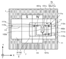
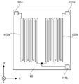
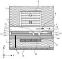
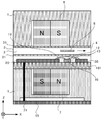
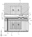
도 1은, 본 발명의 실시형태 1에 관한 자기 센서 장치의 반송 방향에 따른 단면도다. 도 2는, 실시형태 1에 관한 자기 센서 장치의 반송 방향에 직교하는 단면도다. 도면 중의 X축 방향을 반송 방향, Y축 방향을 판독 폭 방향, Z축 방향을 간격 방향으로 한다. 반송 방향, 판독 폭 방향 및 간격 방향은 서로 직교한다. 또한, 간격 방향은, 피검출체(5)가 갖는 자성 패턴을 수직하게 관통하는 방향이다. 반송로(2)는, 지폐 등의 지엽형 매체인 피검출체(5)를 반송하기 위한 것이다. 피검출체(5)는, 하우징(1)의 한쪽의 측면(측벽)에 판독 폭 방향에 걸쳐 설치된 제1 슬릿부(3)로부터 삽입된다. 피검출체(5)는, 반송로(2)를 도면 중의 화살표로 나타낸 반송 방향으로 도시하지 않은 반송수단에 의해 반송되어, 다른쪽의 측면(측벽)에 판독 폭 방향에 걸쳐 설치된 제2 슬릿부(4)로부터 배출된다.1 is a cross-sectional view of a magnetic sensor device according to
영구자석인 제1 자석(6) 및 제2 자석(7)은, 반송로(2)에 대해 서로 반대측에 위치하고, 제1 자석(6)의 자극의 각각과 제2 자석(7)의 이 자극과 다른 자극이 대향한다. 즉, 제1 자석(6)의 N극과 제2 자석(7)의 S극이 대향하고, 제1 자석(6)의 S극과 제2 자석(7)의 N극이 대향한다. 제1 자석(6) 및 제2 자석(7)은 각각, 피검출체(5)로부터 떨어진 위치에 설치되어 있다. 반송로(2)의 제1 자석(6)측과 제2 자석(7)측에 각각 접하도록 전기 실드판(31)이 설치되어 있다.The
제2 자석(7)의 반송로(2)측에 접하도록, 비자성체의 금속 캐리어(191)가 설치되어 있다. 피검출체(5)로부터 떨어진 위치로서, 금속 캐리어(191)의 표면에, 글래스 에폭시 등의 수지로 형성된 다층 기판(9), 및 AMR(Anisotropic MagnetoResistance effect: 이방성 자기저항 효과) 소자(10)가 설치되어 있다. AMR 소자(10)는 표면에 저항을 구비하고, 저항을 흐르는 전류의 방향에 직교하는 자계의 변화에 대응하여 저항값이 변화하는 특성을 갖고 있다.A
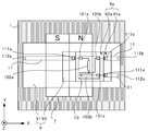
도 3은, 실시형태 1에 관한 자기 센서 장치에 있어서의 금속 캐리어에의 다층 기판과 AMR 소자의 실장 상태를 나타낸 확대도다. 도 3은, 도 1의 일부를 확대한 도면이다. 도 4는, 실시형태 1에 관한 자기 센서 장치에 있어서의 다층 기판과 AMR 소자를 반송로측에서 본 평면도다. 도 5는, 실시형태 1에 관한 자기 센서 장치에 있어서 AMR 소자와 외부 회로의 접속 상태를 나타낸 접속도다. 다층 기판(9)은, 적어도 1층째 기판(91)및 2층째 기판(92)을 구비하고, 금속 캐리어(191)에 고정되어 있다. 다층 기판(9)은, 구멍부(9a)를 갖고, 구멍부(9a)는, 1층째 기판의 구멍부(91a) 및 2층째 기판의 구멍부(92a)로 구성되고, 1층째 기판의 구멍부(91a)의 개구부는 2층째 기판의 구멍부(92a)의 개구부보다도 크다. 이때, 다층 기판(9)은, 3층째 이후의 기판을 구비하도록 구성해도 된다.3 is an enlarged view showing the mounting state of the multilayer substrate and the AMR element in the metal carrier in the magnetic sensor device according to the first embodiment. Fig. 3 is an enlarged view of a part of Fig. Fig. 4 is a plan view of the multilayer substrate and the AMR element in the magnetic sensor device according to
AMR 소자(10)는, 2층째 기판의 구멍부(92a)에 노출되어 있는 금속 캐리어(191)의 표면에 접착재로 고정되어, 다층 기판(9)이 AMR 소자(10)를 둘러싸고 있다. 1층째의 구멍부(91a)와 2층째의 구멍부(92a)는, 수지(13)로 1층째 기판(91)의 표면을 넘지 않도록 봉지되어 있다. AMR 소자(10)의 전극(101a∼101c)은, 1층째 기판의 구멍부(91a)에 노출되어 있는 2층째 기판(92)의 표면에 설치된 전극(111a∼111c)과 각각 전기적 접속수단인 금속 와이어(12)로 접속되어 있다. 전극(111a∼111c)은 전송선로(11)를 통해 다층 기판(9)의 이면에 설치된 접속 패드(112a∼112c)와 접속되어 있다.The
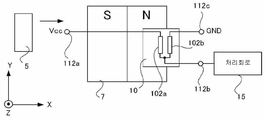
AMR 소자(10)의 저항 102a와 저항 102b는, 각각 사각형 형상의 긴 변이 판독 폭 방향으로 연장되도록 형성된다. 저항 102a, 102b는, 예를 들면 박막으로 형성되어 있다. 저항 102a와 저항 102b는 직렬접속되고, 저항 102a와 저항 102b의 접속점이 전극 101b에 접속되고, 전극 101b는 금속 와이어(12)에 의해 전극 111b에 접속되고, 접속 패드 112b 및 케이블(71)을 거쳐 신호를 처리하는 처리회로(15)에 접속되어 있다. 저항 102a의 다른쪽이 전극 101a에 접속되고, 전극 101a는 금속 와이어(12)에 의해 전극 111a에 접속되고, 접속 패드 112a에 의해 직류 전원 전압 Vcc에 접속되어 있다. 저항 102b의 다른쪽이 전극 101c에 접속되고, 전극 101c는 금속 와이어(12)에 의해 전극 111c에 접속되고, 접속 패드 112c를 경유하여 직류 접지되어 있다.The
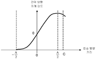
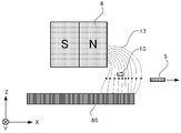
도 6은, 실시형태 1에 관한 자기 센서 장치의 반송로에 있어서 제1 자석과 제2 자석에 의해 생성되는 자계 분포를 도시한 도면이다. 도 7은, 실시형태 1에 관한 자기 센서 장치의 반송로에 있어서 간격 방향의 자계의 반송 방향에 걸치는 강도 변화를 도시한 도면이다. 횡축은 제1 자석(6)의 반송 방향의 중심을 0으로 한 경우의 반송 방향의 거리, 종축은 간격 방향의 자계 강도이다. 도 8은, 실시형태 1에 관한 자기 센서 장치의 검출 원리를 설명하는 자력선 벡터도다. 도 8은, 도 6에 있어서 점선으로 둘러싸인 D부를 확대한 것이다. 이때, 도 6 및 도 8에서는 도 1의 구성요소로부터 자계 분포를 설명하기 위해 필요한 구성요소를 기재하고, 기타는 생략하고 있다.6 is a view showing a magnetic field distribution generated by the first magnet and the second magnet in the conveying path of the magnetic sensor device according to the first embodiment. Fig. 7 is a diagram showing a change in strength over the conveying direction of the magnetic field in the spacing direction in the conveying path of the magnetic sensor device according to the first embodiment. Fig. The abscissa represents the distance in the conveying direction when the center of the
도 6에 나타낸 것과 같이, 제1 자석(6) 및 제2 자석(7)에 의해, 반송로(2)에 있어서, 반송 방향과 직교하는 소정의 방향인 간격 방향의 자계 강도가 소정의 범위인 교차 자계가 생성된다. 예를 들면, 제1 자석(6)의 양 단부에, 자계 강도가 강자계 강도라고 간주할 수 있는 소정의 값 이상인 교차 자계가 생성된다. 또한, AMR 소자(10)는 간격 방향의 자계 강도가 소정의 범위인 강자계 강도 영역에 위치한다. As shown in Fig. 6, the
피검출체(5)는 강자계 강도 영역을 간격 방향의 자계와 교차하도록 통과한다.The to-
도 6에 있어서, AMR 소자(10)가 배치되어 있는 반송 방향에 직교하는 교차 자계에 있어서는, 제2 자석(7)의 N극으로부터 제1 자석(6)의 S극으로 향하는 간격 방향의 성분이 자력선(17)의 주성분으로 되어 있다. 자력선(17)은, 도 8a에 나타낸 것과 같이, 간격 방향으로부터 약간만큼 반송 방향으로 경사져 있기 때문에, 교차 자계의 반송 방향 성분이 AMR 소자(10)의 바이어스 자계로서 작용하고 있다.6, in the crossing magnetic field orthogonal to the conveying direction in which the
피검출체(5)가 근접해 오면, 도 8b에 나타낸 것과 같이, 자력선(17)이 피검출체(5)측으로 경사지기 때문에, 교차 자계의 반송 방향 성분이 작아진다. 피검출체(5)가 떨어져 가면, 도 8c에 나타낸 것과 같이, 자력선(17)이 피검출체(5)측으로 경사지기 때문에, 교차 자계의 반송 방향 성분이 커진다. 교차 자계의 반송 방향 성분의 변화에 의해, 교차 자계의 반송 방향 성분의 변화를 감지하는 AMR 소자(10)의 저항값이 변화하여, 피검출체(5)를 검출할 수 있다.When the to-
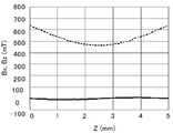
도 9는, 실시형태 1에 관한 자기 센서 장치의 반송로에 있어서 반송 방향 및 간격 방향의 자계의 간격 방향에 걸치는 강도 변화를 도시한 도면이다. 횡축은 간격 방향의 거리 Z(단위: mm)이고, 제2 자석(7)으로부터의 거리를 표시한다. 종축은 반송 방향의 자계 강도 및 간격 방향의 자계 강도(단위: mT)이다. 도 10은, AMR 소자의 인가 자계와 저항 변화율을 도시한 도면이다. 횡축은 인가 자계(단위: mT), 종축은 저항 변화율(단위:%)이다. 도 6에 있어서, 제1 자석(6) 및 제2 자석(7)의 반송 방향의 두께 A=5mm, 제1 자석(6) 및 제2 자석(7)의 간격 방향의 두께 B=10mm, 제1 자석(6)과 제2 자석(7)의 간격 G=5mm이다. 제1 자석(6) 및 제2 자석(7)으로서 네오디뮴 소결 자석을 사용한다. 그리고, 제1 자석(6)의 중심으로부터 반송 방향으로 거리 C=2.7mm 떨어진 위치에서의, 반송 방향의 자계 강도 Bx와 간격 방향의 자계 강도 Bz의 간격 방향에 걸치는 강도 변화를 계산하였다. 자계 강도 Bx가 실선의 그래프이고, 자계 강도 Bz가 점선의 그래프다.Fig. 9 is a diagram showing a change in strength over the gap direction of the magnetic field in the transport direction and the gap direction in the transport path of the magnetic sensor device according to the first embodiment. Fig. The abscissa represents the distance Z in the direction of the distance (unit: mm), and represents the distance from the
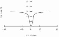
제1 자석(6)과 제2 자석(7)의 간격 G의 중간 지점(Z=2.5mm=G/2)에서 자계 강도 Bx가 0으로 되고 있다. AMR 소자(10)의 포화 자계 강도는, 도 10에 있어서 실선으로 도시한 것과 같이 5mT이고, 도 9에 나타낸 것과 같이, Z=2.65mm 부근에서 Bx가 5mT가 된다. AMR 소자(10)의 위치를 제1 자석(6)과 제2 자석(7)의 간격 G의 중간 지점으로부터 제1 자석(6)의 방향으로 α 이동한 위치로 한다. 0<α<0.15mm로 설정한 경우에는, AMR 소자(10)의 출력이 포화하지 않아, AMR 소자(10)에 적절한 바이어스 자계가 인가된다. 가장 바람직한 것은 AMR 소자(10)의 감도 기울기가 가장 큰 자계 강도 Bx=2.5mT 정도의 바이어스 자계가 인가되는 상태이고, α=0.08mm 부근으로 설정한 경우에, 가장 높은 출력이 얻어진다.The magnetic field strength Bx is 0 at the middle point (Z = 2.5 mm = G / 2) of the gap G between the
피검출체(5)의 자성 패턴이 저항 102a, 102b에 걸렸을 때에 AMR 소자(10)가 검출하는 자계 변화는, 피검출체(5)의 주변의 자계(피검출체(5)에 인가되는 자계)에 비례한다. AMR 소자(10)의 출력을 크게 하기 위해서는, 피검출체(5)에 의해 큰 자계를 가할 필요가 있다. 실시형태 1에 관한 자기 센서 장치에서는, 피검출체(5)와 AMR 소자(10)의 거리가 가까운 경우, 예를 들면, 피검출체(5)가 Z=3mm 부근에 있는 경우, 도 9에서 피검출체(5)에 인가되는 자계 Bz=약 300mT이다. 피검출체(5)와 AMR 소자(10)의 거리가 더 멀어져, 피검출체(5)가 Z=4mm 부근에 있는 경우에는, Bz=약 370mT이다. AMR 소자(10)와 피검출체(5)가 더욱 더 떨어진 위치에 있어서도, 일정 이상의 검출 감도가 유지된다.The change in the magnetic field detected by the
피검출체(5)가 Z=4mm의 지점을 통과하도록 구성한 경우, AMR 소자(10)와 피검출체(5)의 간격은 전술한 기재내용으로부터 1.5mm 정도에 근접하고 있다. 비접촉 상태를 유지하면서 AMR 소자(10)를 보호하는 AMR 소자(10)의 실장방법에 대해 도 3 및 도 4를 사용하여 설명한다.The distance between the
AMR 소자(10)의 두께는 0.5mm 정도이고, 저항 102a, 102b는 AMR 소자(10)의 표면에 형성되어 있다. 저항 102a, 102b가 Z=G/2+α=2.52mm의 지점에 위치하도록, 두께가 2.02mm인 금속 캐리어(191)의 표면에 AMR 소자(10)가 접착되어 있다.The thickness of the
2층째 기판(92)의 두께를 0.5mm로 한다. 2층째 기판(92)의 전극(111a∼111c)과 AMR 소자(10)의 전극(101a∼101c)은 금속 와이어(12)로 접속되어 있다. 2층째 기판(92)의 두께를 AMR 소자(10)의 두께와 동일하게 함으로써, 금속 와이어(12)의 루프 높이를 최소로 할 수 있다.The thickness of the
1층째 기판(91)의 두께는 금속 와이어(12)의 루프 높이와 같은 정도인 0.3mm로 하고, 1층째 기판의 구멍부(91a) 및 2층째 기판의 구멍부(92a)에 점성이 낮은 에폭시계의 수지(13)를 1층째 기판(91)의 표면으로부터 돌출하지 않도록 도포하여, AMR 소자(10)와 금속 와이어(12)를 보호한다. 2층째 기판(92)의 전극(111a∼111c)은 전송선로(11)를 통해 다층 기판(9)의 이면에 설치된 접속 패드(112a∼112c)에 접속되고, 접속 패드(112a∼112c)를 거쳐 전원전압 Vcc, 처리회로(15) 등에 접속되어 있다. 이 실장에 의해, AMR 소자(10)는 보호되고, 또한 피검출체(5)의 반송을 방해하는 돌기물은 없어, 안정적으로 다층 기판(9)의 표면과 피검출체(5) 사이에 1.2mm의 간격이 확보된다.The thickness of the
이와 같이, 피검출체(5)에는 간격 방향의 강자계가 인가되고, AMR 소자(10)와의 거리가 떨어짐에 따라, 한층 더 강자계가 인가되기 때문에, AMR 소자(10)와 피검출체(5)가 떨어져 있어도, 피검출체(5)의 자성 패턴을 검출할 수 있고, 일정 이상의 검출 감도를 유지하는 것이 가능해진다. 또한, AMR 소자(10)에 인가되는 반송 방향의 바이어스 자계의 강도는, 간격 방향의 위치에 따른 변화가 작기 때문에, 조립 정밀도가 향상된다. 더구나, 제1 자석(6)과 제2 자석(7)이 대향하도록 배치하고 있기 때문에, 안정된 자로가 형성되고, 외부의 자성체의 영향을 받기 어려워, 안정적으로 피검출체(5)의 자성 패턴을 검출하는 것이 가능해진다.As the ferromagnetic system in the interval direction is applied to the to-
도 11은, 실시형태 1에 관한 자기 센서 장치에 있어서 미앤더 형상의 저항을 갖는 AMR 소자의 평면도다. AMR 소자(10)의 저항 102a, 102b의 사각형 패턴에 대해서는, 도 11에 나타낸 것과 같이, 긴 변이 판독 폭 방향으로 연장하도록 배치한 미앤더 형상으로 해도 된다. 미앤더 형상이란, 도 11에 나타낸 것과 같은 절곡 모양 형상을 의미한다. 사각형 형상의 저항 102a, 102b와 비교하여, 저항 102a, 102b의 저항값이 증가하여, 고저항값으로 되므로, AMR 소자(10)의 자계 변화의 검출 감도가 향상되어, 자기 센서 장치의 검출 감도가 향상된다.11 is a plan view of an AMR element having a meander-shaped resistance in the magnetic sensor device according to the first embodiment. The square patterns of the
실시형태 1에서는, AMR 소자(10)는 다층 기판(9)의 금속 캐리어(191)의 표면에 접착되어 있다. 저항 변화율이나 포화 자계 강도가 다른 AMR 소자(10)를 사용하여, AMR 소자(10)를 제1 자석(6)에 근접시키는 경우에 있어서는, 금속 캐리어(191)를 설치하지 않고, 제1 자석(6)의 반송로(2)측의 표면에 AMR 소자(10)를 접착하는 구조로 해도 된다.In the first embodiment, the
이때, AMR 소자(10) 대신에, GMR(Giant MagnetoResistance effect: 거대 자기저항 효과) 소자나 TMR(Tunnel MagnetoResistance effect: 터널 자기저항 효과) 소자를 사용해도 된다.
At this time, instead of the
(실시형태 2)(Embodiment 2)
도 12는, 본 발명의 실시형태 2에 관한 자기 센서 장치에 있어서의 다층 기판과 AMR 소자를 반송로측에서 본 평면도다. 도 4와 동일한 구성요소에는 동일한 부호를 붙이고 있다. 도 12에 있어서, AMR 소자(10)의 저항 102a는 사각형 형상의 긴 변이 판독 폭 방향으로 연장하도록 배치되고, 저항 102b는 사각형 형상의 긴 변이 반송 방향으로 연장하도록 배치되고, 저항 102a와 저항 102b가 직렬접속되는 접속점이 AMR 소자(10)의 전극 101b에, 저항 102a의 다른쪽이 전극 101a에, 저항 102b의 다른쪽이 전극 101c에 접속되어 있다.
12 is a plan view of the multilayer substrate and the AMR element in the magnetic sensor device according to
도 13은, 실시형태 2에 관한 자기 센서 장치에 있어서의 AMR 소자와 외부 회로와의 접속 상태를 나타낸 접속도다. 도 5와 동일한 구성요소에는 동일한 부호를 붙이고 있다. 도 12 및 도 13에 있어서, 전극 101a는 금속 와이어(12)에 의해 전극 111a에 접속되고, 접속 패드 112a를 통해 직류 전원 전압 Vcc에 접속되어 있다. 전극 101b는 금속 와이어(12)에 의해 전극 111b에 접속되고, 접속 패드 112b를 통해 신호를 처리하는 처리회로(15)에 접속되어 있다. 전극 101c는 금속 와이어(12)에 의해 전극 111c에 접속되고, 접속 패드 112c를 통해 직류접지되어 있다.13 is a connection diagram showing a connection state between an AMR element and an external circuit in the magnetic sensor device according to the second embodiment. The same components as those in Fig. 5 are denoted by the same reference numerals. 12 and 13, the
실시형태 2에 관한 자기 센서 장치로는, 실시형태 1에 관한 자기 센서 장치 와 마찬가지로, 교차 자계에 있어서 간격 방향의 성분이 자력선(17)의 주성분으로 되고 있다. 또한, 자력선(17)은, 간격 방향으로부터 약간만큼 반송 방향으로 경사져 있기 때문에, 이 자계의 반송 방향 성분이 AMR 소자(10)의 바이어스 자계로서 작용하고 있다. 저항 102a에는 바이어스 자계 Bx가 걸리지만, 저항 102b는 Bx가 자기 감지 방향이 아니기 때문에, 바이어스 자계가 인가되지 않는다. 이 상태에서 피검출체(5)가 반송 방향으로 반송되어, 저항 102a 위에 피검출체(5)의 자성 패턴이 걸리면, 저항 102a 부근의 자계 Bx가 변화하여 저항 102a의 저항값이 변화한다. 한편, 저항 102b 부근의 자계 Bx가 변화하여도, 그 자계 변화를 저항 102b는 감지되지 않기 때문에, 저항 102b의 저항값은 항상 일정하다. 따라서, 저항 102a가 감지하는 자계 변화 만으로 자기 패턴을 검지할 수 있다.In the magnetic sensor device according to the second embodiment, as in the magnetic sensor device according to the first embodiment, the component in the direction of the gap in the crossing magnetic field is the main component of the magnetic force lines 17. Since the magnetic line of
도 14는, 실시형태 2에 관한 자기 센서 장치에 있어서 미앤더 형상의 저항을 갖는 AMR 소자의 평면도다. AMR 소자(10)의 저항 102a, 102b에 대해서는, 도 14에 나타낸 것과 같이, 저항 102a는 긴 변이 판독 폭 방향으로 연장하도록 배치한 미앤더 형상으로 하고, 저항 102b는 긴 변이 반송 방향으로 연장하도록 배치한 미앤더 형상으로 해도 된다. 이 경우, 저항 102a, 102b의 저항값이 사각형 형상의 것보다 증가하여, 고저항값이 되므로, AMR 소자(10)의 자계 변화의 검출 감도가 향상되어, 자기 센서 장치의 검출 감도가 향상된다.
14 is a plan view of an AMR element having a meander-shaped resistance in the magnetic sensor device according to the second embodiment. As shown in Fig. 14, the
(실시형태 3)(Embodiment 3)
도 15는, 본 발명의 실시형태 3에 관한 자기 센서 장치의 반송 방향에 따른 단면도다. 도 1과 동일한 구성요소에는 동일한 부호를 붙이고 있다. 실시형태 3에 관한 자기 센서 장치는, 도 1에 나타낸 실시형태 1에 관한 자기 센서 장치의 구성 이외에, 제1 자석(6)의 측면 중에서, 반송 방향과 직교하는 측면에, 각각 접하는 한 쌍의 자성체인, 제1 자석용 요크(81), 및 제2 자석(7)의 측면 중에서, 반송 방향과 직교하는 측면에, 각각 접하는 한 쌍의 자성체인, 제2 자석용 요크(82)를 더 구비한다.Fig. 15 is a cross-sectional view of the magnetic sensor device according to the third embodiment of the present invention in the carrying direction. Fig. The same components as those in Fig. 1 are denoted by the same reference numerals. In addition to the configuration of the magnetic sensor device according to the first embodiment shown in Fig. 1, the magnetic sensor device according to the third embodiment includes, on the side surface of the
도 16은, 실시형태 3에 관한 자기 센서 장치의 반송로에 있어서 제1 자석용 요크와 제2 자석용 요크에 의해 생성되는 간격 방향의 자계 분포를 도시한 도면이다. 이때, 도 16에서는, 도 15의 구성요소로부터 자계 분포를 설명하기 위해 필요한 구성요소를 기재하고, 기타는 생략하고 있다.16 is a view showing a magnetic field distribution in the direction of the interval generated by the first magnet yoke and the second magnet yoke in the conveying path of the magnetic sensor device according to the third embodiment. At this time, in Fig. 16, the components necessary for explaining the magnetic field distribution from the constituent elements in Fig. 15 are described, and the others are omitted.
도 16에 나타낸 것과 같이, AMR 소자(10)는 간격 방향의 자계 강도가 소정의 범위인 강자계 강도 영역에 위치한다. 피검출체(5)는 강자계 강도 영역을 간격 방향의 자계와 교차하도록 통과한다.As shown in Fig. 16, the
제1 자석용 요크(81)는, 반송 방향의 두께가 P(제1 자석(6) 및 제2 자석(7)의 간격 방향의 두께 B>P)인 판형의 연자성체에 의해 형성된다. 제1 자석용 요크(81)와 제1 자석(6)의 간격 방향의 하단의 위치가 같아지도록, 또는 제1 자석용 요크(81)의 간격 방향의 하단이 제1 자석(6)의 간격 방향의 하단보다 소정의 두께만큼 아래에 위치하도록, 제1 자석용 요크(81)는, 제1 자석(6)의 양측에 접착, 일체 성형, 자력에 의한 흡인 등의 방법으로 부착된다. 제2 자석용 요크(82)는, 반송 방향의 두께가 P인 판형의 연자성체에 의해 형성된다. 제2 자석용 요크(82)와 제2 자석(7)의 간격 방향의 상단의 위치가 같아지도록, 또는 제2 자석용 요크(82)의 간격 방향의 상단이 제2 자석(7)의 간격 방향의 상단보다 소정의 두께만큼 위에 위치하도록, 제2 자석용 요크(82)는, 제2 자석(7)의 양측에 접착, 일체성형, 자력에 의한 흡인 등의 방법으로 부착된다.The
본 구성에 따르면, 제1 자석(6) 및 제2 자석(7)의 측면에서 발생한 자력선(17)이, 반송 방향의 두께가 P인 제1 자석용 요크(81) 및 제2 자석용 요크(82)에 모인다. 자력선(17)은 도 16에 나타낸 것과 같이, 제1 자석(6)의 N극측과 접하고 있는 제1 자석용 요크(81)의 단부로부터 발생하여, 제2 자석(7)의 S극측과 접하고 있는 제2 자석용 요크(82)의 단부를 향하는 루프를 그린다. 또한, 자력선(17)은 제2 자석(7)의 N극측과 접하고 있는 제2 자석용 요크(82)의 단부로부터 각각 발생하여, 제1 자석(6)의 S극측과 접하고 있는 제1 자석용 요크(81)의 단부를 향하는 루프를 그린다. 실시형태 3에 관한 자기 센서 장치에 있어서도, 도 8에 나타낸 실시형태 1에 관한 자기 센서 장치가 사용하는 원리와 같은 원리로 지폐 등의 피검출체(5)의 검출이 가능하다. 제1 자석용 요크(81) 및 제2 자석용 요크(82)를 설치함으로써, 제1 자석(6)및 제2 자석(7) 만을 대향시킨 경우에 비해 한층 더 큰 자계가 피검출체(5)에 인가되고, 또한 조립 정밀도가 개선된다.The
도 17은, 실시형태 3에 관한 자기 센서 장치의 반송로에 있어서 반송 방향 및 간격 방향의 자계의 간격 방향에 걸치는 강도 변화를 도시한 도면이다. 횡축은 간격 방향의 거리 Z(단위: mm)이고, 제2 자석용 요크(82)로부터의 거리를 표시한다. 종축은 반송 방향의 자계 강도 및 간격 방향의 자계 강도(단위: mT)이다. 도 16에 있어서, 제1 자석(6) 및 제2 자석(7)의 반송 방향의 두께 A=5mm, 제1 자석(6) 및 제2 자석(7)의 간격 방향의 두께 B=10mm, 제1 자석용 요크(81) 및 제2 자석용 요크(82)의 반송 방향의 두께 P=3mm이다. 제1 자석용 요크(81)의 간격 방향의 하단은 제1 자석(6)의 간격 방향의 하단보다 Q=1mm만큼 아래에 위치하고, 제2 자석용 요크(82)의 간격 방향의 상단은 제2 자석(7)의 간격 방향의 상단보다 Q=1mm만큼 위에 위치한다. 제1 자석용 요크(81)와 제2 자석용 요크(82)와의 간격 G=5mm이다. 제1 자석(6) 및 제2 자석(7)으로서 네오디뮴 소결 자석을 사용한다. 그리고, 제1 자석(6)의 중심으로부터 반송 방향으로 거리 C=4.0mm 떨어진 위치에서의, 반송 방향의 자계 강도 Bx와 간격 방향의 자계 강도 Bz의 간격 방향에 걸치는 강도 변화를 계산하였다. 자계 강도 성분 Bx가 실선의 그래프이고, 자계 강도 성분 Bz가 점선의 그래프다.Fig. 17 is a diagram showing a change in strength over the gap direction of the magnetic field in the transport direction and the gap direction in the transport path of the magnetic sensor device according to the third embodiment. Fig. The horizontal axis indicates the distance Z in the direction of the distance (unit: mm), and indicates the distance from the
자계 강도는, 제1 자석용 요크(81)와 제2 자석용 요크(82)의 간격 G의 중간 지점(Z=2.5mm=G/2)에서 자계 강도 Bx가 0으로 되어 있다. AMR 소자(10)의 포화 자계 강도는, 도 10에 있어서 실선으로 도시한 것과 같이 5mT이고, 도 17에 나타낸 것과 같이, Z=3.0mm 부근에서 Bx가 5mT가 된다. AMR 소자(10)의 위치를 제1 자석용 요크(81)와 제2 자석용 요크(82)의 간격 G의 중간 지점에서 제1 자석용 요크(81)의 방향으로 α 이동한 위치로 한다. 0<α<0.5mm로 설정한 경우에는, AMR 소자(10)의 출력이 포화하지 않아, AMR 소자(10)에 적절한 바이어스 자계가 인가된다. 이것은, 실시형태 1에 관한 자기 센서 장치의 조립 정밀도(0<α<0.15mm)와 비교하면 대폭적으로 개선되어 있는 것을 알 수 있다. 또한, 가장 바람직한 것은 AMR 소자(10)의 감도 기울기가 가장 큰 자계 강도 Bx=2.5mT 정도의 바이어스 자계가 인가되는 상태로서, α=0.25mm 부근으로 설정한 경우에, 가장 높은 출력이 얻어진다.The magnetic field intensity Bx is 0 at the midpoint (Z = 2.5 mm = G / 2) of the gap G between the
피검출체(5)의 자성 패턴이 저항 102a, 102b에 걸렸을 때에 AMR 소자(10)가 검출하는 자계 변화는, 피검출체(5)의 주변의 자계(피검출체(5)에 인가되는 자계)에 비례한다. AMR 소자(10)의 출력을 크게 하기 위해서는, 피검출체(5)에 의해 큰 자계를 가할 필요가 있다. 실시형태 2에 관한 자기 센서 장치에서는, 피검출체(5)와 AMR 소자(10)의 거리가 가까운 경우, 예를 들면 피검출체(5)가 Z=3mm 부근에 있는 경우, 도 17에서 피검출체(5)에 인가되는 자계는 Bz=약 480mT이다. 피검출체(5)와 AMR 소자(10)의 거리가 더 멀어져, 피검출체(5)가 Z=4mm 부근에 있는 경우에는, Bz=약 540mT이다. AMR 소자(10)와 피검출체(5)가 한층 더 떨어진 위치에 있어도, 일정 이상의 검출 감도가 유지된다. 이것은, 실시형태 1에 관한 자기 센서 장치에 있어서 피검출체(5)에 인가되는 자계와 비교하여 대폭적으로 강화되어 있는 것을 알 수 있다. 그 결과, 안정된 출력을 얻을 수 있다.The change in the magnetic field detected by the
또한, 제1 자석용 요크(81) 및 제2 자석용 요크(82)를 각각 제1 자석(6) 및 제2 자석(7)의 양 측면에 부착함으로써, 제1 자석(6) 및 제2 자석(7)의 판독 폭 방향의 자력의 격차를 균일화할 수 있다. 특히 라인형 자기 센서의 경우, 각 채널 사이의 바이어스 자계의 격차를 억제하여, 결과적으로 라인 사이의 출력의 격차를 억제할 수 있어, 수율 향상, 코스트 삭감에 이어진다.
By attaching the
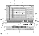
(실시형태 4)(Fourth Embodiment)
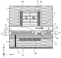
도 18은, 본 발명의 실시형태 4에 관한 자기 센서 장치의 반송 방향에 따른 단면도다. 도 1과 동일한 구성요소에는 동일한 부호를 붙이고 있다. 실시형태 4에 관한 자기 센서 장치는, 도 1에 나타낸 실시형태 1에 관한 자기 센서 장치와 달리 자석(8)과 자성체(80)가 대향하고 있다. 이때, 자성체(80)로서, 예를 들면, 철 등의 연자성체를 사용한다.18 is a cross-sectional view of the magnetic sensor device according to the fourth embodiment of the present invention in the carrying direction. The same components as those in Fig. 1 are denoted by the same reference numerals. The magnetic sensor device according to the fourth embodiment is different from the magnetic sensor device according to the first embodiment shown in Fig. 1 in that the
도 19는, 실시형태 4에 관한 자기 센서 장치의 반송로에 있어서의 자석과 자성체에 의해 생성되는 자계 분포를 도시한 도면이다. 이때, 도 19에서는, 도 18의 구성요소로부터 자계 분포를 설명하기 위해 필요한 구성요소를 기재하고, 기타는 생략하고 있다. 도 19에 있어서, 대향하는 자석(8)과 자성체(80)에 의해 생성되는 간격 방향의 자계의 반송 방향에 걸치는 강도 변화는, 도 7과 마찬가지로, 자석(8)의 반송 방향의 중앙 부근에서 0이 되고, 자석(8)의 양 단부를 향해 절대값이 증대해가는 분포를 갖는다.19 is a diagram showing a magnetic field distribution generated by a magnet and a magnetic body in a conveying path of the magnetic sensor device according to the fourth embodiment. 19, components necessary for explaining the magnetic field distribution from the components in Fig. 18 are described, and the other components are omitted. 19, the change in the strength in the direction of the magnetic field in the direction of the gap generated by the opposing
도 19에 나타낸 것과 같이, AMR 소자(10)는 간격 방향의 자계 강도가 소정의 범위인 강자계 강도 영역에 위치한다. 피검출체(5)는 강자계 강도 영역을 간격 방향의 자계와 교차하도록 통과한다.As shown in Fig. 19, the
도 19에 있어서, AMR 소자(10)가 배치되어 있는 반송 방향에 직교하는 교차 자계에 있어서는, 자석(8)의 N극으로부터 자성체(80)로 향하는 간격 방향의 성분이 자력선(17)의 주성분으로 되고 있다. 실시형태 4에 관한 자기 센서 장치에 있어서도, 도 8에 나타낸 실시형태 1에 관한 자기 센서 장치가 사용하는 원리와 같은 원리로 지폐 등의 피검출체(5)의 검출이 가능하다.19, in the crossing magnetic field orthogonal to the conveying direction in which the
실시형태 4에 관한 자기 센서 장치에 따르면, 바이어스 자석을 한쪽에만 배치하고, 대향측에는 저렴한 철 등의 연자성체를 배치하기 때문에, 자기 센서 장치의 제조 코스트를 삭감하는 것이 가능하다.
According to the magnetic sensor device of
(실시형태 5)(Embodiment 5)
도 20은, 본 발명의 실시형태 5에 관한 자기 센서 장치의 반송 방향에 따른 단면도다. 실시형태 5에 관한 자기 센서 장치는, 도 18에 나타낸 실시형태 4에 관한 자기 센서 장치의 구성 이외에, 자석(8)의 측면 중에서, 반송 방향과 직교하는 측면에, 각각 접하는 한 쌍의 자성체인, 자석용 요크(83)를 배치하고 있다. 요크의 형상은 실시형태 3에 관한 자기 센서 장치가 구비한 제1 자석용 요크(81)와 같다. 도 18과 동일한 구성요소에는 동일한 부호를 붙이고 있다.Fig. 20 is a cross-sectional view of the magnetic sensor device according to
도 21은, 실시형태 5에 관한 자기 센서 장치의 반송로에 있어서의 자석용 요크와 자성체에 의해 생성되는 자계 분포를 도시한 도면이다. 이때, 도 21에서는, 도 20의 구성요소로부터 자계 분포를 설명하기 위해 필요한 구성요소를 기재하고, 기타는 생략하고 있다.21 is a view showing a magnetic field distribution generated by the magnet yoke and the magnetic body in the conveying path of the magnetic sensor device according to the fifth embodiment. At this time, in Fig. 21, the components necessary for explaining the magnetic field distribution from the constituent elements in Fig. 20 are described, and the others are omitted.
도 21에 나타낸 것과 같이, AMR 소자(10)는 간격 방향의 자계 강도가 소정의 범위인 강자계 강도 영역에 위치한다. 피검출체(5)는 강자계 강도 영역을 간격 방향의 자계와 교차하도록 통과한다.As shown in Fig. 21, the
도 21에 있어서, AMR 소자(10)가 배치되어 있는 반송 방향에 직교하는 교차 자계에 있어서는, 자석(8)의 N극측에 접하는 자석용 요크(83)로부터 자성체(80)로 향하는 간격 방향의 성분이 자력선(17)의 주성분으로 되고 있다. 실시형태 5에 관한 자기 센서 장치에 있어서도, 도 8에 나타낸 실시형태 1에 관한 자기 센서 장치가 사용하는 원리와 같은 원리로 지폐 등의 피검출체(5)의 검출이 가능하다.21, in the crossing magnetic field orthogonal to the conveying direction in which the
본 구성에 따르면, 자석(8)의 측면에서 발생한 자력선(17)이, 반송 방향의 두께가 P인 자석용 요크(83)에 모이고, 자력선(17)은 도 21에 나타낸 것과 같이, 자석(8)의 N극측과 접하고 있는 자석용 요크(83)의 단부로부터 발생하여, 자성체(80)를 향하는 루프를 그린다. 자석용 요크(83)를 설치함으로써, 실시형태 4에 관한 자기 센서 장치와 비교하여 보다 큰 자계가 피검출체(5)에 인가되고, 또한 조립 정밀도가 개선된다.According to this configuration, the
또한, 실시형태 5에 관한 자기 센서 장치에 따르면, 바이어스 자석을 한 쪽에만 배치하고, 대향측에는 저렴한 철 등의 연자성체를 배치하기 때문에, 자기 센서 장치의 제조 코스트를 삭감하는 것이 가능하다.
Further, according to the magnetic sensor device of
(실시형태 6)(Embodiment 6)
도 22는, 본 발명의 실시형태 6에 관한 자기 센서 장치의 반송 방향에 따른 단면도다. 실시형태 6에 관한 자기 센서 장치는, 도 18에 나타낸 실시형태 4에 관한 자기 센서 장치가 구비하는 자석(8)의 방향을 변경하고, 자석(8)의 어느 한쪽의 자극과 자성체(80)가 대향하도록 배치한 것이다. 도 18과 동일한 구성요소에는 동일한 부호를 붙이고 있다.22 is a cross-sectional view of the magnetic sensor device according to
도 23은, 실시형태 6에 관한 자기 센서 장치의 반송로에 있어서의 자석과 자성체에 의해 생성되는 자계 분포를 도시한 도면이다. 이때, 도 23에서는, 도 22의 구성요소로부터 자계 분포를 설명하기 위해 필요한 구성요소를 기재하고, 기타는 생략하고 있다. 도 23에 있어서, 간격 방향의 자계 강도는, 자석(8)의 반송 방향의 중앙 부근에서 절대값이 최대가 되고, 자석(8)의 양 단부를 향해 감소해가는 분포를 갖는다.23 is a diagram showing a magnetic field distribution generated by a magnet and a magnetic body in a conveying path of the magnetic sensor device according to the sixth embodiment. At this time, in Fig. 23, components necessary for explaining the magnetic field distribution from the constituent elements in Fig. 22 are described, and the others are omitted. 23, the magnetic field strength in the spacing direction has a distribution in which the absolute value becomes maximum near the center in the conveying direction of the
도 23에 나타낸 것과 같이, AMR 소자(10)는 간격 방향의 자계 강도가 소정의 범위인 강자계 강도 영역에 위치한다. 피검출체(5)는 강자계 강도 영역을 간격 방향의 자계와 교차하도록 통과한다.As shown in Fig. 23, the
도 23에 있어서, AMR 소자(10)가 배치되어 있는 반송 방향에 직교하는 교차 자계에 있어서는, 자석(8)의 N극으로부터 자성체(80)로 향하는 간격 방향의 성분이 자력선(17)의 주성분으로 되고 있다. 실시형태 6에 관한 자기 센서 장치에 있어서도, 도 8에 나타낸 실시형태 1에 관한 자기 센서 장치가 사용하는 원리와 같은 원리로 지폐 등의 피검출체(5)의 검출이 가능하다.
23, in the crossing magnetic field orthogonal to the conveying direction in which the
(실시형태 7)(Seventh Embodiment)
도 24는, 본 발명의 실시형태 7에 관한 자기 센서 장치에 있어서의 다층 기판과 AMR 소자를 반송로측에서 본 평면도다. 실시형태 7에 관한 자기 센서 장치는, 도 12에 나타낸 실시형태 2에 관한 자기 센서 장치가 구비하는 AMR 소자(10)를 어레이 형상으로 배치한 것이다. 도 24에 있어서 도 12와 동일한 구성요소에는 동일한 부호를 붙이고 있다. 도 24에 있어서, 다층 기판(9)의 구멍부(9a)에, 판독 폭 방향에 걸쳐 복수의 AMR 소자(10)가 어레이 형상으로 설치되어 있다. 동작에 대해서는, 본 발명의 실시형태 2에 관한 자기 센서 장치와 같다. 이때, AMR 소자(10)의 저항 102a, 102b와 전극 101a∼101c의 접속 방법은 도 12에 나타낸 것에 한정되지 않고, 도 4에 도시하는 것과 같이 접속해도 된다. 또한, 저항 102a, 102b의 사각형 형상의 패턴은, 도 11 또는 도 14와 같이 미앤더 형상으로 해도 된다. 또한, 반송로(2)에 대해 서로 반대측에 위치하는 한 쌍의 자석, 또는 반송로(2)에 대해 서로 반대측에 위치하는 자석 및 자성체의 배치는, 실시형태 1∼6에 나타낸 어느쪽의 배치이어도 된다.24 is a plan view of the multilayer substrate and the AMR element in the magnetic sensor device according to the seventh embodiment of the present invention, as viewed from the conveying path side. The magnetic sensor device according to
도 24에 있어서는, 모든 AMR 소자(10)가 1개의 구멍부(9a)에 위치하고 있고, 다층 기판(9)이 모든 AMR 소자(10)를 일괄적으로 둘러싸고 있지만, 다층 기판(9)이 AMR 소자(10)를 1개씩 둘러싸도록 구성해도 된다. 또한, 다층 기판(9)이 복수의 구멍부(9a)를 구비하고, 복수의 AMR 소자(10)가 각각의 구멍부(9a)에 위치하고, 다층 기판(9)이 복수의 AMR 소자(10)를 각각 일괄적으로 둘러싸도록 구성해도 된다.24, all of the
이와 같이, AMR 소자(10)를 판독 폭 방향으로 복수개 어레이 형상으로 배치한 라인형의 자기 센서 장치로 함으로써, 검지 폭이 넓어진다.
As described above, the detection width is widened by using a line-type magnetic sensor device in which a plurality of
(실시형태 8)(Embodiment 8)
도 25는, 본 발명의 실시형태 8에 관한 자기 센서 장치의 반송 방향에 따른 단면도다. 실시형태 8에 관한 자기 센서 장치는, 도 18에 나타낸 실시형태 4에 관한 자기 센서 장치가 구비하는 자석(8)과 자성체(80)를 교체하여, 자기 센서 장치의 상하를 반전시킨 것이다. 도 18과 동일한 구성요소에는 동일한 부호를 붙이고 있다. 이때, 자성체(80)로서, 예를 들면, 철 등의 연자성체를 사용한다.Fig. 25 is a cross-sectional view of the magnetic sensor device according to the eighth embodiment of the present invention in the carrying direction. Fig. The magnetic sensor device according to
도 26은, 실시형태 8에 관한 자기 센서 장치의 반송로에 있어서의 자석과 자성체에 의해 생성되는 자계 분포를 도시한 도면이다. 이때, 도 26에서는, 도 25의 구성요소로부터 자계 분포를 설명하기 위해 필요한 구성요소를 기재하고, 기타는 생략하고 있다. 도 26에 있어서, 대향하는 자석(8)과 자성체(80)의 간격 방향의 자계의 반송 방향에 걸치는 강도 변화는, 도 7과 마찬가지로, 자석(8)의 반송 방향의 중앙 부근에서 0이 되고, 자석(8)의 양 단부를 향해 절대값이 증대해가는 분포를 갖는다.26 is a diagram showing a magnetic field distribution generated by a magnet and a magnetic body in a conveying path of the magnetic sensor device according to the eighth embodiment. 26, elements necessary for explaining the magnetic field distribution from the constituent elements of Fig. 25 are described, and the others are omitted. 26, the change in the strength of the magnetic field in the direction of the gap between the opposing
도 26에 나타낸 것과 같이, AMR 소자(10)는 간격 방향의 자계 강도가 소정의 범위인 강자계 강도 영역에 위치한다. 피검출체(5)는 강자계 강도 영역을 간격 방향의 자계와 교차하도록 통과한다.As shown in Fig. 26, the
도 26에 있어서, AMR 소자(10)가 배치되어 있는 반송 방향에 직교하는 교차 자계에 있어서는, 자석(8)의 N극으로부터 자성체(80)로 향하는 간격 방향의 성분이 자력선(17)의 주성분으로 되고 있다. 실시형태 8에 관한 자기 센서 장치에 있어서도, 도 8에 나타낸 실시형태 1에 관한 자기 센서 장치가 사용하는 원리와 같은 원리로 지폐 등의 피검출체(5)의 검출이 가능하다.26, in the crossing magnetic field orthogonal to the conveying direction in which the
실시형태 8에 관한 자기 센서 장치에 따르면, 실시형태 4에 관한 자기 센서 장치와 마찬가지로, 바이어스 자석을 한 쪽에만 배치하고, 대향측에는 저렴한 철 등의 연자성체를 배치하기 때문에, 자기 센서 장치의 제조 코스트를 삭감하는 것이 가능하다.According to the magnetic sensor device according to the eighth embodiment, since bias magnets are disposed on only one side and soft magnetic material elements such as inexpensive iron are disposed on the opposite sides as in the magnetic sensor device according to the fourth embodiment, Can be reduced.
실시형태 5에 관한 자기 센서 장치와 마찬가지로, 실시형태 8에 관한 자기 센서 장치가 구비하는 자석(8)의 측면 중에서, 반송 방향과 직교하는 측면에, 각각 접하는 한 쌍의 자성체인, 자석용 요크를 배치한 경우에는, 실시형태 5에 관한 자기 센서 장치와 같은 작용 효과가 얻어진다.As in the magnetic sensor device according to
실시형태 6에 관한 자기 센서 장치와 마찬가지로, 실시형태 8에 관한 자기 센서 장치가 구비하는 자석(8)의 착자 방향을 간격 방향으로 한 경우에는, 실시형태 6에 관한 자기 센서 장치와 같은 작용 효과가 얻어진다.
When the magnetization direction of the
(실시형태 9)(Embodiment 9)
도 27은, 본 발명의 실시형태 9에 관한 자기 센서 장치의 반송 방향에 따른 단면도다. 도 28은, 실시형태 9에 관한 자기 센서 장치에 있어서 금속 캐리어에의 단층 기판과 AMR 소자의 실장 상태를 나타낸 확대도다. 도 27 및 도 28에 있어서, 각각 도 1 및 도 3과 동일한 구성요소에는 동일한 부호를 붙이고 있다. 실시형태 9에 관한 자기 센서 장치는, 실시형태 1에 관한 자기 센서 장치가 구비하는 다층 기판(9) 대신에, 단층 기판(20)을 구비한다.27 is a cross-sectional view of the magnetic sensor device according to the ninth embodiment of the present invention in the carrying direction. 28 is an enlarged view showing the mounting state of the single layer substrate and the AMR element on the metal carrier in the magnetic sensor device according to the ninth embodiment; In Figs. 27 and 28, the same components as those in Figs. 1 and 3 are denoted by the same reference numerals. A magnetic sensor device according to
금속 캐리어(191)의 표면에, 단층 기판(20) 및 AMR 소자(10)가 설치되어 있다. 단층 기판(20)은, 구멍부(20a)를 갖는다. AMR 소자(10)는, 구멍부(20a)에 노출되어 있는 금속 캐리어(191)의 표면에 접착제로 고정되고, 단층 기판(20)이 AMR 소자(10)를 둘러싸고 있다. 도 4와 마찬가지로, AMR 소자(10)의 전극(101a∼101c)은, 단층 기판(20)의 표면에 설치된 전극(111a∼111c)과 각각 금속 와이어(12)로 접속되어 있다. 전극 111a∼111c는 전송선로(11)를 통해 단층 기판(20)의 이면에 설치된 접속 패드(112a∼112c)와 접속되어 있다. 접속 패드 112a는 직류 전원 전압 Vcc에 접속되고, 접속 패드 112b는 처리회로(15)에 접속되고, 접속 패드 112c는 직류접지되어 있다. 또한, AMR 소자(10)와 금속 와이어(12)는, 수지(13)에 의해 봉지되고 있어, 보호되어 있다.On the surface of the
실시형태 9에 관한 자기 센서 장치에 있어서도, 실시형태 1에 관한 자기 센서 장치와 동일한 작용 효과가 얻어진다.
Also in the magnetic sensor device according to the ninth embodiment, the same operational effects as those of the magnetic sensor device according to the first embodiment can be obtained.
(실시형태 10)(Embodiment 10)
도 29는, 본 발명의 실시형태 10에 관한 자기 센서 장치의 반송 방향에 따른 단면도이고, 도 30은, 실시형태 10에 관한 자기 센서 장치에 있어서의 금속 캐리어에의 단층 기판과 AMR 소자의 실장 상태를 나타낸 확대도다. 도 29 및 도 30에 있어서, 각각 도 1 및 도 3과 동일한 구성요소에는 동일한 부호를 붙이고 있다. 실시형태 10에 관한 자기 센서 장치는, 실시형태 1에 관한 자기 센서 장치가 구비하는 다층 기판(9) 대신에, 단층 기판(20)을 구비한다.Fig. 29 is a cross-sectional view of the magnetic sensor device according to the tenth embodiment of the present invention in the carrying direction, Fig. 30 is a cross-sectional view of the monolayer substrate and the AMR element mounted on the metal carrier in the magnetic sensor device according to the tenth embodiment Fig. 29 and 30, the same components as those in Figs. 1 and 3 are denoted by the same reference numerals. The magnetic sensor device according to
금속 캐리어(191)의 표면에, 단층 기판(20) 및 AMR 소자(10)가 설치되어 있다. 단층 기판(20)은, 구멍부(20a)를 갖는다. AMR 소자(10)는, 구멍부(20a)에 노출되어 있는 금속 캐리어(191)의 표면에 접착제로 고정되고, 단층 기판(20)이 AMR 소자(10)를 둘러싸고 있다. 도 4와 마찬가지로, AMR 소자(10)의 전극(101a∼101c)은, 단층 기판(20)의 표면에 설치된 전극(111a∼111c)과 각각 금속 탭(21)으로 접속되어 있다. 전극 111a∼111c는 전송선로(11)를 통해 단층 기판(20)의 이면에 설치된 접속 패드(112a∼112c)와 접속되어 있다. 접속 패드 112a는 직류 전원 전압 Vcc에 접속되고, 접속 패드 112b는 처리회로(15)에 접속되고, 접속 패드 112c는 직류접지되어 있다.On the surface of the
실시형태 10에 관한 자기 센서 장치에 있어서도, 실시형태 1에 관한 자기 센서 장치와 같은 작용 효과가 얻어진다. 더구나, AMR 소자(10)의 전극(101a∼101c)과 단층 기판(20)의 표면에 설치된 전극(111a∼111c)이 금속 탭(21)으로 접속되어 있으므로, AMR 소자(10)와 전기 실드판(31)의 틈이 작아지고, AMR 소자(10)와 피검출체(5)의 거리가 짧아져, AMR 소자(10)의 출력이 커지므로, 검출 감도가 향상된다.
The same effects as those of the magnetic sensor device according to the first embodiment can be obtained also in the magnetic sensor device according to the tenth embodiment. In addition, since the
(실시형태 11)(Embodiment 11)
도 31은, 본 발명의 실시형태 11에 관한 자기 센서 장치의 반송 방향에 따른 단면도다. 도 32는, 실시형태 11에 관한 자기 센서 장치에 있어서의 단층 기판과 AMR 소자의 실장 상태를 나타낸 확대도다. 도 31 및 도 32에 있어서, 각각 도 1 및 도 3과 동일한 구성요소에는 동일한 부호를 붙이고 있다. 실시형태 11에 관한 자기 센서 장치는, 실시형태 1에 관한 자기 센서 장치가 구비하는 다층 기판(9) 대신에, 단층 기판(20)을 구비한다. 또한, 실시형태 11에 관한 자기 센서 장치는, 금속 캐리어(191)를 구비하지 않는다.Fig. 31 is a cross-sectional view of the magnetic sensor device according to
AMR 소자(10)는, 단층 기판(20)의 표면에 접착제로 고정되어 있다. 도 4와 마찬가지로, AMR 소자(10)의 전극(101a∼101c)은, 단층 기판(20)의 표면에 설치된 전극(111a∼111c)과 각각 금속 와이어(12)로 접속되어 있다. 전극 111a∼111c는 전송선로(11)를 통해 단층 기판(20)의 이면에 설치된 접속 패드(112a∼112c)와 접속되어 있다. 접속 패드 112a는 직류 전원 전압 Vcc에 접속되고, 접속 패드 112b는 처리회로(15)에 접속되고, 접속 패드 112c는 직류접지되어 있다. 또한, AMR 소자(10)와 금속 와이어(12)는, 수지(13)에 의해 봉지되어 있어, 보호되어 있다.The
실시형태 11에 관한 자기 센서 장치에 있어서도, 실시형태 1에 관한 자기 센서 장치와 같은 작용 효과가 얻어진다. 또한, 금속 캐리어(191)를 설치하지 않기 때문에, 구조를 간단화하는 것이 가능해진다.
The same effects as those of the magnetic sensor device according to the first embodiment can be obtained also in the magnetic sensor device according to the eleventh embodiment. Further, since the
(실시형태 12)(Embodiment 12)
도 33은, 본 발명의 실시형태 12에 관한 자기 센서 장치의 반송 방향에 따른 단면도다. 실시형태 12에 관한 자기 센서 장치는, 실시형태 11에 관한 자기 센서 장치가 구비하는 제1 자석(6) 및 제2 자석(7)의 방향을 변화시켜, 제1 자석(6)의 어느쪽인가의 자극과 제2 자석(7)의 이 자극과 다른 자극이 대향하도록 배치한다. 그리고, 제2 자석(7)의 표면에 AMR 소자(10)를 설치하고, 단층 기판(20)이 AMR 소자(10)를 둘러싸도록 배치한 것이다. 도 34는, 실시형태 12에 관한 자기 센서 장치에 있어서 단층 기판과 AMR 소자의 실장 상태를 나타낸 확대도다. 도 33 및 도 34에 있어서, 도 31 및 도 32와 동일한 구성요소에는 동일한 부호를 붙이고 있다.Fig. 33 is a cross-sectional view of the magnetic sensor device according to
단층 기판(20)은 제2 자석(7)에 고정되어 있고, 구멍부(20a)를 갖는다. AMR 소자(10)는, 구멍부(20a)에 노출되어 있는 제2 자석(7)의 표면에 접착제로 고정되고, 단층 기판(20)이 AMR 소자(10)를 둘러싸고 있다. 도 4와 마찬가지로, AMR 소자(10)의 전극(101a∼101c)은, 단층 기판(20)의 표면에 설치된 전극(111a∼111c)과 각각 금속 와이어(12)로 접속되어 있다. 전극(111a∼111c)은 전송선로(11)를 통해 단층 기판(20)의 이면에 설치된 접속 패드(112a∼112c)와 접속되어 있다. 접속 패드 112a는 직류 전원 전압 Vcc에 접속되고, 접속 패드 112b는 처리회로(15)에 접속되고, 접속 패드 112c는 직류접지되어 있다. 또한, AMR 소자(10)와 금속 와이어(12)는, 수지(13)에 의해 봉지되고 있어, 보호되어 있다.The
제1 자석(6)과 제2 자석(7)은 다른 극이 대향하고 있으므로, 도 23과 마찬가지로 피검출체(5) 및 AMR 소자(10)에 반송 방향의 자계가 인가되므로, 실시형태 6에 관한 자기 센서 장치와 같은 작용 효과가 얻어진다.
Since the first and
(실시형태 13)(Embodiment 13)
도 35는, 본 발명의 실시형태 13에 관한 자기 센서 장치의 반송 방향에 따른 단면도다. 실시형태 12에 관한 자기 센서 장치가 구비하는 금속 와이어(12) 대신에, 금속 탭(21)으로 AMR 소자(10)의 전극(101a∼101c)과 단층 기판(20)의 표면에 설치된 전극(111a∼111c)을 접속한 것이다. 도 36은, 실시형태 13에 관한 자기 센서 장치에 있어서의 단층 기판과 AMR 소자의 실장 상태를 나타낸 확대도다. 도 35 및 도 36에 있어서, 도 33 및 도 34와 동일한 구성요소에는 동일한 부호를 붙이고 있다.35 is a cross-sectional view of the magnetic sensor device according to
단층 기판(20)은 제2 자석(7)에 고정되어 있고, 구멍부(20a)를 갖는다. AMR 소자(10)는, 구멍부(20a)에 노출되어 있는 제2 자석(7)의 표면에 접착제로 고정되고, 단층 기판(20)이 AMR 소자(10)를 둘러싸고 있다. 도 4와 마찬가지로, AMR 소자(10)의 전극(101a∼101c)은, 단층 기판(20)의 표면에 설치된 전극(111a∼111c)과 각각 금속 탭(21)으로 접속되어 있다. 전극 111a∼111c는 전송선로(11)를 통해 단층 기판(20)의 이면에 설치된 접속 패드(112a∼112c)와 접속되어 있다. 접속 패드 112a는 직류 전원 전압 Vcc에 접속되고, 접속 패드 112b는 처리회로(15)에 접속되고, 접속 패드 112c는 직류접지되어 있다.The
제1 자석(6)과 제2 자석(7)은 다른 극이 대향하고 있으므로, 도 23과 마찬가지로 피검출체(5) 및 AMR 소자(10)에 반송 방향의 자계가 인가되므로, 실시형태 6에 관한 자기 센서 장치와 같은 작용 효과가 얻어진다. 더구나, AMR 소자(10)의 전극(101a∼101c)과 단층 기판(20)의 표면에 설치된 전극(111a∼111c)이 금속 탭(21)으로 접속되어 있다. 그 때문에, AMR 소자(10)와 전기 실드판(31)의 틈이 작아지고, AMR 소자(10)와 피검출체(5)의 거리가 짧아져, AMR 소자(10)의 출력이 커지므로, 검출 감도가 향상된다.Since the first and
상기 실시형태는, 모두 본 발명의 취지의 범위 내에서 각종의 변형이 가능하다. 상기 실시형태는 본 발명을 설명하기 위한 것이고, 본 발명의 범위를 한정하는 것을 의도한 것은 아니다. 본 발명의 범위는 실시형태보다도 첨부한 청구항에 의해 표시된다. 청구항의 범위 내, 및 발명의 청구항과 균등한 범위에서 행해지는 각종 변형은 본 발명의 범위에 포함된다.All of the above-described embodiments can be modified in various ways within the scope of the present invention. The foregoing embodiments are intended to illustrate the present invention and are not intended to limit the scope of the invention. The scope of the invention is indicated by the appended claims rather than the embodiments. Various modifications made within the scope of the claims and the equivalents of the claims of the invention are included in the scope of the present invention.
본 출원은, 2011년 5월 16일에 출원된, 명세서, 특허청구범위, 도면 및 요약서를 포함하는 일본국 특허출원 2011-109628호, 및 2012년 3월 29일에 출원된, 명세서, 특허청구범위, 도면 및 요약서를 포함하는 일본국 특허출원 2012-077356호에 근거한 우선권을 주장하는 것이다. 이것의 기초가 되는 특허출원의 개시 내용은 참조에 의해 전체로서 본 출원에 포함된다.
This application claims the benefit of Japanese Patent Application No. 2011-109628, filed on May 16, 2011, including specifications, claims, drawings and summary, and the specification, And claims the priority based on Japanese Patent Application No. 2012-077356, which includes scope, drawings and summary. The disclosures of which are incorporated herein by reference in their entirety.
본 발명은, 자성 패턴을 갖는 피검출체와 자기 저항 효과 소자가 소정의 거리만큼 떨어져 있는 비접촉 상태에서, 피검출체의 자성 패턴을 검출하는 자기 센서 장치에 적합하게 채용될 수 있다.
INDUSTRIAL APPLICABILITY The present invention can be suitably applied to a magnetic sensor device that detects a magnetic pattern of a detected object in a non-contact state in which the magnetically resistive element having a magnetic pattern and the magnetoresistive element are separated by a predetermined distance.
1 하우징
2 반송로
3 제1 슬릿부
4 제2 슬릿부
5 피검출체
6 제1 자석
7 제2 자석
8 자석
9 다층 기판
9a 구멍부
10 AMR 소자
11 전송선로
12 금속 와이어
13 수지
15 처리회로
17 자력선
20 단층 기판
20a 구멍부
21 금속 탭
31 전기 실드판
71 케이블
80 자성체
81 제1 자석용 요크
82 제2 자석용 요크
83 자석용 요크
91 1층째 기판
91a 1층째 기판의 구멍부
92 2층째 기판
92a 2층째 기판의 구멍부
101a, 101b, 101c 전극
102a, 102b 저항
111a, 111b, 111c 전극
112a, 112b, 112c 접속 패드
191 금속 캐리어1 Housing
2 carrier path
3 First slit part
4 second slit portion
5 Detected body
6 First magnet
7 Second magnet
8 magnets
9 multilayer substrate
9a hole
10 AMR element
11 transmission line
12 metal wire
13 resin
15 processing circuit
17 magnetic lines
20 single layer substrate
20a hole portion
21 Metal tap
31 Electrical shield plate
71 Cable
80 magnetic body
81 yoke for first magnet
82 yoke for second magnet
83 yoke for magnets
91 First layer substrate
91a hole portion of the first layer substrate
92 Second layer substrate
92a hole portion of the second layer substrate
101a, 101b, 101c electrodes
102a, 102b Resistance
111a, 111b, and 111c electrodes
112a, 112b, 112c connecting pads
191 metal carrier
Claims (3)
각각의 자극이 상기 반송로에 대향하는 자석과,
상기 자석의 측면 중에서, 상기 피검출체의 반송 방향과 직교하는 측면에 접하는 제1 자성체와,
상기 반송로에 대해 상기 제1 자성체와 반대측에 위치하는 제2 자성체와,
상기 반송로에 있어서, 상기 반송 방향과 직교하는 방향으로서, 상기 자성 패턴을 수직하게 관통하는 방향인 간격 방향에 있어서의 제1 자성체와 제2 자성체에 의해 생성되는 자계 강도가 소정의 범위인 교차 자계에 있어서, 상기 제2 자성체와 상기 반송로 사이에 위치하고, 상기 피검출체의 상기 자성 패턴에 의한 상기 교차 자계의 상기 반송 방향의 성분의 변화를, 저항값의 변화로서 검출하는 자기 저항 효과 소자와,
상기 자기 저항 효과 소자에 접속되고, 상기 자기 저항 효과 소자가 검출한 상기 저항값의 변화를 출력하는 출력부를 구비한 자기 센서 장치.
A conveying path for conveying a member to be detected including a magnetic pattern,
A magnet in which each magnetic pole faces the conveying path,
A first magnetic body in contact with a side surface of the magnet facing the conveying direction of the to-be-detected object,
A second magnetic body positioned on the side opposite to the first magnetic body with respect to the conveying path,
The magnetic field intensity generated by the first magnetic body and the second magnetic body in the direction perpendicular to the magnetic pattern in the direction perpendicular to the conveying direction is set to a cross magnetic field A magnetoresistance effect element which is located between the second magnetic body and the conveying path and detects a change in the component of the crossing magnetic field in the conveying direction by the magnetic pattern of the detected member as a change in the resistance value ,
And an output section connected to the magneto-resistance effect element and outputting a change in the resistance value detected by the magneto-resistance effect element.
제2 자석을 더 구비하고,
상기 자석은 제1 자석이며,
상기 제1 자석 및 상기 제2 자석은, 상기 반송로에 대해 서로 반대측에 위치하고, 상기 제1 자석의 자극의 각각과 상기 제2 자석의 상기 자극과 다른 자극이 대향하고,
상기 제1 자성체는, 상기 제1 자석의 측면 중에서, 상기 반송 방향과 직교하는 측면에 각각 접하는 한 쌍의 제1 자석용 요크이고,
상기 제2 자성체는, 상기 제2 자석의 측면 중에서, 상기 반송 방향과 직교하는 측면에 각각 접하는 한 쌍의 제2 자석용 요크인 자기 센서 장치.
The method according to claim 1,
Further comprising a second magnet,
The magnet is a first magnet,
Wherein the first magnet and the second magnet are located on opposite sides of the conveying path, each of the magnetic poles of the first magnet and the magnetic poles of the second magnet are opposed to each other,
Wherein the first magnetic body is a pair of first magnet yokes which are respectively in contact with side surfaces perpendicular to the carrying direction among the side surfaces of the first magnet,
And the second magnetic body is a pair of yokes for second magnets which are respectively in contact with sides of the side surface of the second magnet perpendicular to the carrying direction.
상기 자석의 자극의 각각과 상기 제2 자성체가 대향하고,
상기 제1 자성체는, 상기 자석의 측면 중에서, 상기 반송 방향과 직교하는 측면에 각각 접하는 한 쌍의 자석용 요크인 자기 센서 장치.
The method according to claim 1,
Each of the magnetic poles of the magnet and the second magnetic body face each other,
Wherein the first magnetic body is a pair of yokes for magnet which are respectively in contact with side surfaces perpendicular to the carrying direction among side surfaces of the magnet.
Applications Claiming Priority (5)
| Application Number | Priority Date | Filing Date | Title |
|---|---|---|---|
| JPJP-P-2011-109628 | 2011-05-16 | ||
| JP2011109628 | 2011-05-16 | ||
| JPJP-P-2012-077356 | 2012-03-29 | ||
| JP2012077356A JP5867235B2 (en) | 2011-05-16 | 2012-03-29 | Magnetic sensor device |
| PCT/JP2012/062126 WO2012157558A1 (en) | 2011-05-16 | 2012-05-11 | Magnetic sensor device |
Related Parent Applications (1)
| Application Number | Title | Priority Date | Filing Date |
|---|---|---|---|
| KR1020137029138A Division KR20140002024A (en) | 2011-05-16 | 2012-05-11 | Magnetic sensor device |
Publications (1)
| Publication Number | Publication Date |
|---|---|
| KR20150103324A true KR20150103324A (en) | 2015-09-09 |
Family
ID=47176878
Family Applications (2)
| Application Number | Title | Priority Date | Filing Date |
|---|---|---|---|
| KR1020137029138A KR20140002024A (en) | 2011-05-16 | 2012-05-11 | Magnetic sensor device |
| KR1020157022947A KR20150103324A (en) | 2011-05-16 | 2012-05-11 | Magnetic sensor device |
Family Applications Before (1)
| Application Number | Title | Priority Date | Filing Date |
|---|---|---|---|
| KR1020137029138A KR20140002024A (en) | 2011-05-16 | 2012-05-11 | Magnetic sensor device |
Country Status (8)
| Country | Link |
|---|---|
| US (1) | US9244135B2 (en) |
| EP (1) | EP2711728B1 (en) |
| JP (1) | JP5867235B2 (en) |
| KR (2) | KR20140002024A (en) |
| CN (1) | CN103842838B (en) |
| CA (1) | CA2827487A1 (en) |
| RU (1) | RU2013151002A (en) |
| WO (1) | WO2012157558A1 (en) |
Families Citing this family (27)
| Publication number | Priority date | Publication date | Assignee | Title |
|---|---|---|---|---|
| CN104105977B (en) * | 2012-02-13 | 2017-09-26 | 株式会社村田制作所 | magnetic sensing device |
| US9279866B2 (en) | 2012-04-09 | 2016-03-08 | Mitsubishi Electric Corporation | Magnetic sensor |
| US9664533B2 (en) | 2013-02-07 | 2017-05-30 | Mitsubishi Electric Corporation | Magnetic sensor device |
| JP5793735B2 (en) * | 2013-02-19 | 2015-10-14 | ジーエヌエス有限会社 | Magnetic foreign matter inspection apparatus and magnetic foreign matter inspection method |
| CN105026924B (en) * | 2013-03-22 | 2019-01-08 | 光荣株式会社 | Magnetic characteristic detection device |
| JP6034731B2 (en) * | 2013-03-26 | 2016-11-30 | 浜松光電株式会社 | Magnetic detection device |
| JP5677652B1 (en) * | 2013-04-05 | 2015-02-25 | 三菱電機株式会社 | Image reading device |
| JP6075225B2 (en) * | 2013-06-25 | 2017-02-08 | 三菱電機株式会社 | Magnetic sensor device |
| CN203551758U (en) * | 2013-07-26 | 2014-04-16 | 江苏多维科技有限公司 | Single-magnetoresistance TMR magnetic field sensor chip and magnetic head of counterfeit detector |
| JP6301709B2 (en) * | 2014-04-09 | 2018-03-28 | グローリー株式会社 | Magnetic quality discrimination device and magnetic quality discrimination method |
| DE112015002254T5 (en) * | 2014-05-13 | 2017-03-02 | Mitsubishi Electric Corporation | MAGNETIC SENSOR DEVICE |
| CN106461742B (en) * | 2014-06-18 | 2019-05-28 | 三菱电机株式会社 | Magnet sensor arrangement and its manufacturing method |
| JP6316429B2 (en) * | 2014-07-25 | 2018-04-25 | 三菱電機株式会社 | Magnetic sensor device |
| US9689903B2 (en) * | 2014-08-12 | 2017-06-27 | Analog Devices, Inc. | Apparatus and methods for measuring current |
| CN107873085B (en) * | 2015-02-02 | 2020-03-10 | 三菱电机株式会社 | Magnetic sensor device |
| JP6125119B2 (en) * | 2015-03-26 | 2017-05-10 | 三菱電機株式会社 | System design support apparatus, system design support method, and system design support program |
| CN107037381A (en) | 2015-12-29 | 2017-08-11 | 爱盛科技股份有限公司 | Magnetic field sensing device and sensing method thereof |
| DE112016006539T5 (en) * | 2016-03-03 | 2018-11-15 | Tdk Corporation | MAGNETIC SENSOR |
| CN109073716B (en) * | 2016-03-30 | 2021-09-17 | 三菱电机株式会社 | Magnetic sensor device |
| US11522901B2 (en) * | 2016-09-23 | 2022-12-06 | OPSWAT, Inc. | Computer security vulnerability assessment |
| WO2018096862A1 (en) * | 2016-11-25 | 2018-05-31 | 三菱電機株式会社 | Magnetic sensor device |
| US10341725B2 (en) | 2016-12-27 | 2019-07-02 | Rovi Guides, Inc. | Methods and systems for determining user engagement based on user interactions during different time intervals |
| US10051326B2 (en) | 2016-12-27 | 2018-08-14 | Rovi Guides, Inc. | Methods and systems for determining user engagement based on user interactions during different advertisement slots |
| JP6490130B2 (en) * | 2017-03-24 | 2019-03-27 | Tdk株式会社 | Magnetic sensor |
| US10788517B2 (en) | 2017-11-14 | 2020-09-29 | Analog Devices Global Unlimited Company | Current measuring apparatus and methods |
| US10712369B2 (en) | 2018-03-23 | 2020-07-14 | Analog Devices Global Unlimted Company | Current measurement using magnetic sensors and contour intervals |
| US11639974B1 (en) | 2020-03-30 | 2023-05-02 | Mitsubishi Electric Corporation | Magnetic sensor device |
Family Cites Families (37)
| Publication number | Priority date | Publication date | Assignee | Title |
|---|---|---|---|---|
| SU920596A1 (en) | 1980-07-08 | 1982-04-15 | Физико-технический институт АН ТССР | Magnetoresistor |
| JPS582994A (en) | 1981-06-29 | 1983-01-08 | 株式会社東芝 | Detector for existing in sheet paper |
| US4416044A (en) | 1981-04-02 | 1983-11-22 | The Air Preheater Company, Inc. | Cast recuperator tube |
| JPS6241266Y2 (en) * | 1981-04-30 | 1987-10-22 | ||
| JPS6241266A (en) | 1985-08-19 | 1987-02-23 | Asahi Chem Ind Co Ltd | Electrically conductive high-molecular material |
| JP2668252B2 (en) * | 1987-12-25 | 1997-10-27 | 東洋通信機株式会社 | Magnetic sensor |
| JP2921262B2 (en) | 1992-06-04 | 1999-07-19 | 株式会社村田製作所 | Long magnetic sensor |
| JPH06167302A (en) | 1992-12-01 | 1994-06-14 | Smc Corp | Detecting apparatus of position of moving body |
| JPH06231336A (en) * | 1993-02-01 | 1994-08-19 | Murata Mfg Co Ltd | Magnetic sensor |
| DE4407759A1 (en) | 1993-03-10 | 1994-09-15 | Honeywell Inc | Magnetic sensor |
| JPH06350159A (en) * | 1993-06-10 | 1994-12-22 | Sankyo Seiki Mfg Co Ltd | Magnetic sensor |
| JPH07210833A (en) * | 1994-01-11 | 1995-08-11 | Murata Mfg Co Ltd | Magnetic sensor device |
| JPH0815590A (en) * | 1994-06-29 | 1996-01-19 | Olympus Optical Co Ltd | Optical element positioning device |
| JP3314548B2 (en) | 1994-09-16 | 2002-08-12 | 松下電器産業株式会社 | Magnetic detector |
| JP3487452B2 (en) | 1994-12-19 | 2004-01-19 | 株式会社デンソー | Magnetic detector |
| JPH08249602A (en) | 1995-03-06 | 1996-09-27 | Mitsubishi Electric Corp | Magnetic storing/reproducing method and magnetic reproducing device used for it, magnetic storing medium, and its manufacturing method |
| JP2823539B2 (en) | 1995-12-01 | 1998-11-11 | エスエムシー株式会社 | Position detection device |
| JPH1019601A (en) * | 1996-07-02 | 1998-01-23 | Yazaki Corp | Magnetic detector |
| JP3311614B2 (en) | 1996-11-21 | 2002-08-05 | 矢崎総業株式会社 | Magnetic detection device and magnetoresistive element |
| JP4024964B2 (en) * | 1998-07-28 | 2007-12-19 | キヤノン電子株式会社 | Magnetic sensor for magnetic ink detection, signal processing method thereof, and magnetic ink detection device |
| RU2175455C2 (en) | 1998-12-08 | 2001-10-27 | Институт физики металлов Уральского отделения РАН | Magnetoresistive converter to read information from magnetic carriers |
| JP4697498B2 (en) * | 1999-07-06 | 2011-06-08 | ニッコーシ株式会社 | Magnetic sensor device |
| JP2002131406A (en) | 2000-10-20 | 2002-05-09 | Sankyo Seiki Mfg Co Ltd | Magnetism detector |
| JP4500472B2 (en) * | 2001-08-13 | 2010-07-14 | アルプス電気株式会社 | Magnetic switch and magnetic sensor |
| JP2005129009A (en) | 2003-09-30 | 2005-05-19 | Fuji Electric Retail Systems Co Ltd | Paper sheet discriminating device and method |
| DE102004032484B3 (en) * | 2004-07-05 | 2005-11-24 | Infineon Technologies Ag | Sensor and method for manufacturing a sensor |
| US7019607B2 (en) * | 2004-08-09 | 2006-03-28 | Honeywell International Inc. | Precision non-contact digital switch |
| DE102006022336B8 (en) * | 2006-02-28 | 2015-12-31 | Infineon Technologies Ag | Magnetic field sensor and sensor arrangement with the same |
| JP4894040B2 (en) * | 2006-12-13 | 2012-03-07 | 浜松光電株式会社 | Magnetic sensor |
| US8378674B2 (en) | 2007-05-28 | 2013-02-19 | Mitsubishi Electric Corporation | Magnetic field detection device |
| JP5175350B2 (en) | 2008-07-29 | 2013-04-03 | アルプス電気株式会社 | Magnetic detector |
| JP4735686B2 (en) * | 2008-09-02 | 2011-07-27 | 株式会社村田製作所 | Magnetic sensor |
| JP4798191B2 (en) | 2008-09-02 | 2011-10-19 | 株式会社村田製作所 | Magnetic sensor device |
| WO2010052797A1 (en) * | 2008-11-10 | 2010-05-14 | グローリー株式会社 | Magnetic property detection apparatus |
| DE102008058538A1 (en) * | 2008-11-21 | 2010-05-27 | Bernstein Ag | Giant magnetoresistance sensor for detection of magnetic material, has sensor element and temperature sensor element arranged in sensor housing with multilayered structure, where elements are enclosed by embedding layer |
| US9222993B2 (en) * | 2010-07-30 | 2015-12-29 | Mitsubishi Electric Corporation | Magnetic substance detection device |
| WO2012015012A1 (en) | 2010-07-30 | 2012-02-02 | 三菱電機株式会社 | Magnetic sensor device |
-
2012
- 2012-03-29 JP JP2012077356A patent/JP5867235B2/en active Active
- 2012-05-11 RU RU2013151002/28A patent/RU2013151002A/en not_active Application Discontinuation
- 2012-05-11 US US14/009,441 patent/US9244135B2/en active Active
- 2012-05-11 KR KR1020137029138A patent/KR20140002024A/en active Application Filing
- 2012-05-11 CA CA2827487A patent/CA2827487A1/en not_active Abandoned
- 2012-05-11 EP EP12784930.5A patent/EP2711728B1/en active Active
- 2012-05-11 CN CN201280023413.0A patent/CN103842838B/en active Active
- 2012-05-11 KR KR1020157022947A patent/KR20150103324A/en active IP Right Grant
- 2012-05-11 WO PCT/JP2012/062126 patent/WO2012157558A1/en active Application Filing
Also Published As
| Publication number | Publication date |
|---|---|
| EP2711728A1 (en) | 2014-03-26 |
| EP2711728A4 (en) | 2015-04-15 |
| US9244135B2 (en) | 2016-01-26 |
| US20140028308A1 (en) | 2014-01-30 |
| JP5867235B2 (en) | 2016-02-24 |
| EP2711728B1 (en) | 2021-03-17 |
| CN103842838A (en) | 2014-06-04 |
| JP2012255770A (en) | 2012-12-27 |
| KR20140002024A (en) | 2014-01-07 |
| CN103842838B (en) | 2016-03-16 |
| CA2827487A1 (en) | 2012-11-22 |
| WO2012157558A1 (en) | 2012-11-22 |
| RU2013151002A (en) | 2015-06-27 |
Similar Documents
| Publication | Publication Date | Title |
|---|---|---|
| KR20150103324A (en) | Magnetic sensor device | |
| KR101376987B1 (en) | magnetic sensor device | |
| US9279866B2 (en) | Magnetic sensor | |
| JP5516773B2 (en) | Magnetic sensor device | |
| JP6265484B2 (en) | Magnetic sensor module | |
| CN106537166B (en) | Magnetic sensor device | |
| JP5799882B2 (en) | Magnetic sensor device | |
| US20190204396A1 (en) | Magnetoresistive effect element unit and magnetoresistive effect element device | |
| JP2012215405A (en) | Magnetic sensor device | |
| JP5861551B2 (en) | Magnetic sensor device | |
| JP2013047610A (en) | Magnetic balance type current sensor | |
| WO2021199757A1 (en) | Magnetic sensor device | |
| CN114207857A (en) | Magnetic sensor device | |
| WO2019049414A1 (en) | Magnetic sensor and current sensor provided with same |
Legal Events
| Date | Code | Title | Description |
|---|---|---|---|
| A107 | Divisional application of patent | ||
| A201 | Request for examination | ||
| E902 | Notification of reason for refusal | ||
| E701 | Decision to grant or registration of patent right |