KR20150066547A - Current switching transistor - Google Patents
Current switching transistor Download PDFInfo
- Publication number
- KR20150066547A KR20150066547A KR1020157010907A KR20157010907A KR20150066547A KR 20150066547 A KR20150066547 A KR 20150066547A KR 1020157010907 A KR1020157010907 A KR 1020157010907A KR 20157010907 A KR20157010907 A KR 20157010907A KR 20150066547 A KR20150066547 A KR 20150066547A
- Authority
- KR
- South Korea
- Prior art keywords
- semiconductor material
- terminal
- terminals
- current
- electronic device
- Prior art date
Links
- 239000000463 material Substances 0.000 claims abstract description 144
- 239000004065 semiconductor Substances 0.000 claims abstract description 133
- 239000004020 conductor Substances 0.000 claims abstract description 35
- 238000007639 printing Methods 0.000 claims abstract description 27
- 238000004519 manufacturing process Methods 0.000 claims abstract description 21
- 238000000576 coating method Methods 0.000 claims abstract description 11
- 239000011248 coating agent Substances 0.000 claims abstract description 9
- 239000000758 substrate Substances 0.000 claims description 38
- 238000000034 method Methods 0.000 claims description 35
- 238000006243 chemical reaction Methods 0.000 claims description 20
- 238000010030 laminating Methods 0.000 claims description 12
- 239000011810 insulating material Substances 0.000 claims description 9
- 239000002245 particle Substances 0.000 claims description 4
- 239000011856 silicon-based particle Substances 0.000 claims description 3
- 238000000151 deposition Methods 0.000 claims description 2
- 239000000203 mixture Substances 0.000 claims description 2
- 239000011236 particulate material Substances 0.000 claims 1
- 239000000976 ink Substances 0.000 description 15
- 230000005669 field effect Effects 0.000 description 12
- 229910052751 metal Inorganic materials 0.000 description 11
- 239000002184 metal Substances 0.000 description 11
- XUIMIQQOPSSXEZ-UHFFFAOYSA-N Silicon Chemical compound [Si] XUIMIQQOPSSXEZ-UHFFFAOYSA-N 0.000 description 10
- 230000006870 function Effects 0.000 description 10
- 239000000123 paper Substances 0.000 description 10
- 229910052710 silicon Inorganic materials 0.000 description 10
- 239000010703 silicon Substances 0.000 description 10
- BQCADISMDOOEFD-UHFFFAOYSA-N Silver Chemical compound [Ag] BQCADISMDOOEFD-UHFFFAOYSA-N 0.000 description 8
- 238000013461 design Methods 0.000 description 8
- 230000008569 process Effects 0.000 description 8
- 239000004332 silver Substances 0.000 description 8
- 238000007650 screen-printing Methods 0.000 description 7
- 229910052709 silver Inorganic materials 0.000 description 7
- 150000002739 metals Chemical class 0.000 description 6
- 238000004806 packaging method and process Methods 0.000 description 5
- 239000010409 thin film Substances 0.000 description 5
- 239000002131 composite material Substances 0.000 description 4
- 238000010586 diagram Methods 0.000 description 4
- 239000002657 fibrous material Substances 0.000 description 4
- 239000005543 nano-size silicon particle Substances 0.000 description 4
- -1 polyethylene terephthalate Polymers 0.000 description 4
- 238000012545 processing Methods 0.000 description 4
- 238000000427 thin-film deposition Methods 0.000 description 4
- 230000008859 change Effects 0.000 description 3
- 238000011161 development Methods 0.000 description 3
- 239000000835 fiber Substances 0.000 description 3
- 238000003475 lamination Methods 0.000 description 3
- 238000000059 patterning Methods 0.000 description 3
- 229920000139 polyethylene terephthalate Polymers 0.000 description 3
- 239000005020 polyethylene terephthalate Substances 0.000 description 3
- 229910001316 Ag alloy Inorganic materials 0.000 description 2
- RYGMFSIKBFXOCR-UHFFFAOYSA-N Copper Chemical compound [Cu] RYGMFSIKBFXOCR-UHFFFAOYSA-N 0.000 description 2
- PXHVJJICTQNCMI-UHFFFAOYSA-N Nickel Chemical compound [Ni] PXHVJJICTQNCMI-UHFFFAOYSA-N 0.000 description 2
- KDLHZDBZIXYQEI-UHFFFAOYSA-N Palladium Chemical compound [Pd] KDLHZDBZIXYQEI-UHFFFAOYSA-N 0.000 description 2
- 239000004698 Polyethylene Substances 0.000 description 2
- ATJFFYVFTNAWJD-UHFFFAOYSA-N Tin Chemical compound [Sn] ATJFFYVFTNAWJD-UHFFFAOYSA-N 0.000 description 2
- RTAQQCXQSZGOHL-UHFFFAOYSA-N Titanium Chemical compound [Ti] RTAQQCXQSZGOHL-UHFFFAOYSA-N 0.000 description 2
- 229910045601 alloy Inorganic materials 0.000 description 2
- 239000000956 alloy Substances 0.000 description 2
- 229920006217 cellulose acetate butyrate Polymers 0.000 description 2
- 238000005234 chemical deposition Methods 0.000 description 2
- 229910052802 copper Inorganic materials 0.000 description 2
- 239000010949 copper Substances 0.000 description 2
- 230000005684 electric field Effects 0.000 description 2
- 238000001459 lithography Methods 0.000 description 2
- 239000002105 nanoparticle Substances 0.000 description 2
- 238000005289 physical deposition Methods 0.000 description 2
- 229920003223 poly(pyromellitimide-1,4-diphenyl ether) Polymers 0.000 description 2
- 229920000573 polyethylene Polymers 0.000 description 2
- 229920000642 polymer Polymers 0.000 description 2
- 238000007736 thin film deposition technique Methods 0.000 description 2
- 239000011135 tin Substances 0.000 description 2
- 229910052718 tin Inorganic materials 0.000 description 2
- 239000010936 titanium Substances 0.000 description 2
- 229910052719 titanium Inorganic materials 0.000 description 2
- 239000002023 wood Substances 0.000 description 2
- 210000002268 wool Anatomy 0.000 description 2
- 229910000838 Al alloy Inorganic materials 0.000 description 1
- 229910000851 Alloy steel Inorganic materials 0.000 description 1
- JBRZTFJDHDCESZ-UHFFFAOYSA-N AsGa Chemical compound [As]#[Ga] JBRZTFJDHDCESZ-UHFFFAOYSA-N 0.000 description 1
- ZOXJGFHDIHLPTG-UHFFFAOYSA-N Boron Chemical compound [B] ZOXJGFHDIHLPTG-UHFFFAOYSA-N 0.000 description 1
- OKTJSMMVPCPJKN-UHFFFAOYSA-N Carbon Chemical compound [C] OKTJSMMVPCPJKN-UHFFFAOYSA-N 0.000 description 1
- 229920000742 Cotton Polymers 0.000 description 1
- 229910000881 Cu alloy Inorganic materials 0.000 description 1
- 229910001218 Gallium arsenide Inorganic materials 0.000 description 1
- DGAQECJNVWCQMB-PUAWFVPOSA-M Ilexoside XXIX Chemical compound C[C@@H]1CC[C@@]2(CC[C@@]3(C(=CC[C@H]4[C@]3(CC[C@@H]5[C@@]4(CC[C@@H](C5(C)C)OS(=O)(=O)[O-])C)C)[C@@H]2[C@]1(C)O)C)C(=O)O[C@H]6[C@@H]([C@H]([C@@H]([C@H](O6)CO)O)O)O.[Na+] DGAQECJNVWCQMB-PUAWFVPOSA-M 0.000 description 1
- GPXJNWSHGFTCBW-UHFFFAOYSA-N Indium phosphide Chemical compound [In]#P GPXJNWSHGFTCBW-UHFFFAOYSA-N 0.000 description 1
- FYYHWMGAXLPEAU-UHFFFAOYSA-N Magnesium Chemical compound [Mg] FYYHWMGAXLPEAU-UHFFFAOYSA-N 0.000 description 1
- 229910000861 Mg alloy Inorganic materials 0.000 description 1
- ZOKXTWBITQBERF-UHFFFAOYSA-N Molybdenum Chemical compound [Mo] ZOKXTWBITQBERF-UHFFFAOYSA-N 0.000 description 1
- 229920000784 Nomex Polymers 0.000 description 1
- 229920001609 Poly(3,4-ethylenedioxythiophene) Polymers 0.000 description 1
- 239000004642 Polyimide Substances 0.000 description 1
- 229910001069 Ti alloy Inorganic materials 0.000 description 1
- HCHKCACWOHOZIP-UHFFFAOYSA-N Zinc Chemical compound [Zn] HCHKCACWOHOZIP-UHFFFAOYSA-N 0.000 description 1
- 229920005822 acrylic binder Polymers 0.000 description 1
- 229910052782 aluminium Inorganic materials 0.000 description 1
- XAGFODPZIPBFFR-UHFFFAOYSA-N aluminium Chemical compound [Al] XAGFODPZIPBFFR-UHFFFAOYSA-N 0.000 description 1
- 230000003466 anti-cipated effect Effects 0.000 description 1
- 229910052787 antimony Inorganic materials 0.000 description 1
- WATWJIUSRGPENY-UHFFFAOYSA-N antimony atom Chemical compound [Sb] WATWJIUSRGPENY-UHFFFAOYSA-N 0.000 description 1
- 239000004760 aramid Substances 0.000 description 1
- 229920003235 aromatic polyamide Polymers 0.000 description 1
- JRPBQTZRNDNNOP-UHFFFAOYSA-N barium titanate Chemical compound [Ba+2].[Ba+2].[O-][Ti]([O-])([O-])[O-] JRPBQTZRNDNNOP-UHFFFAOYSA-N 0.000 description 1
- 229910002113 barium titanate Inorganic materials 0.000 description 1
- 230000004888 barrier function Effects 0.000 description 1
- 230000008901 benefit Effects 0.000 description 1
- 230000015572 biosynthetic process Effects 0.000 description 1
- 229910052796 boron Inorganic materials 0.000 description 1
- 239000005388 borosilicate glass Substances 0.000 description 1
- 238000003490 calendering Methods 0.000 description 1
- 229910052799 carbon Inorganic materials 0.000 description 1
- 229920002678 cellulose Polymers 0.000 description 1
- 239000001913 cellulose Substances 0.000 description 1
- 229920002301 cellulose acetate Polymers 0.000 description 1
- 239000000919 ceramic Substances 0.000 description 1
- 229910010293 ceramic material Inorganic materials 0.000 description 1
- 239000002800 charge carrier Substances 0.000 description 1
- 239000011093 chipboard Substances 0.000 description 1
- 238000004891 communication Methods 0.000 description 1
- 150000001875 compounds Chemical class 0.000 description 1
- 238000002508 contact lithography Methods 0.000 description 1
- UIPVMGDJUWUZEI-UHFFFAOYSA-N copper;selanylideneindium Chemical compound [Cu].[In]=[Se] UIPVMGDJUWUZEI-UHFFFAOYSA-N 0.000 description 1
- 230000001419 dependent effect Effects 0.000 description 1
- 230000008021 deposition Effects 0.000 description 1
- 238000001035 drying Methods 0.000 description 1
- 238000004049 embossing Methods 0.000 description 1
- 239000003822 epoxy resin Substances 0.000 description 1
- 239000004744 fabric Substances 0.000 description 1
- 239000000945 filler Substances 0.000 description 1
- 238000001914 filtration Methods 0.000 description 1
- 238000007647 flexography Methods 0.000 description 1
- 239000011888 foil Substances 0.000 description 1
- 229910052732 germanium Inorganic materials 0.000 description 1
- GNPVGFCGXDBREM-UHFFFAOYSA-N germanium atom Chemical compound [Ge] GNPVGFCGXDBREM-UHFFFAOYSA-N 0.000 description 1
- 239000011521 glass Substances 0.000 description 1
- 230000006872 improvement Effects 0.000 description 1
- 229910052738 indium Inorganic materials 0.000 description 1
- APFVFJFRJDLVQX-UHFFFAOYSA-N indium atom Chemical compound [In] APFVFJFRJDLVQX-UHFFFAOYSA-N 0.000 description 1
- 238000002347 injection Methods 0.000 description 1
- 239000007924 injection Substances 0.000 description 1
- 238000007641 inkjet printing Methods 0.000 description 1
- 229910052500 inorganic mineral Inorganic materials 0.000 description 1
- 230000002452 interceptive effect Effects 0.000 description 1
- 238000010147 laser engraving Methods 0.000 description 1
- 238000010329 laser etching Methods 0.000 description 1
- 238000007644 letterpress printing Methods 0.000 description 1
- 239000007788 liquid Substances 0.000 description 1
- 229910052749 magnesium Inorganic materials 0.000 description 1
- 239000011777 magnesium Substances 0.000 description 1
- 238000004377 microelectronic Methods 0.000 description 1
- 238000003801 milling Methods 0.000 description 1
- 239000011707 mineral Substances 0.000 description 1
- 239000011490 mineral wool Substances 0.000 description 1
- 229910052750 molybdenum Inorganic materials 0.000 description 1
- 239000011733 molybdenum Substances 0.000 description 1
- 239000012802 nanoclay Substances 0.000 description 1
- 239000002073 nanorod Substances 0.000 description 1
- 239000002071 nanotube Substances 0.000 description 1
- 239000002070 nanowire Substances 0.000 description 1
- 229910052759 nickel Inorganic materials 0.000 description 1
- 239000004763 nomex Substances 0.000 description 1
- 239000004745 nonwoven fabric Substances 0.000 description 1
- 238000007649 pad printing Methods 0.000 description 1
- 229910052763 palladium Inorganic materials 0.000 description 1
- 239000011087 paperboard Substances 0.000 description 1
- 230000003071 parasitic effect Effects 0.000 description 1
- 150000002989 phenols Chemical class 0.000 description 1
- 238000000206 photolithography Methods 0.000 description 1
- 229920000301 poly(3-hexylthiophene-2,5-diyl) polymer Polymers 0.000 description 1
- 229920000515 polycarbonate Polymers 0.000 description 1
- 239000004417 polycarbonate Substances 0.000 description 1
- 229920000647 polyepoxide Polymers 0.000 description 1
- 239000011112 polyethylene naphthalate Substances 0.000 description 1
- 229920001721 polyimide Polymers 0.000 description 1
- 229920001296 polysiloxane Polymers 0.000 description 1
- 239000010453 quartz Substances 0.000 description 1
- 230000009467 reduction Effects 0.000 description 1
- 230000004044 response Effects 0.000 description 1
- 229910052594 sapphire Inorganic materials 0.000 description 1
- 239000010980 sapphire Substances 0.000 description 1
- 150000004760 silicates Chemical class 0.000 description 1
- VYPSYNLAJGMNEJ-UHFFFAOYSA-N silicon dioxide Inorganic materials O=[Si]=O VYPSYNLAJGMNEJ-UHFFFAOYSA-N 0.000 description 1
- 239000011734 sodium Substances 0.000 description 1
- 229910052708 sodium Inorganic materials 0.000 description 1
- 239000007787 solid Substances 0.000 description 1
- 238000004528 spin coating Methods 0.000 description 1
- 239000007921 spray Substances 0.000 description 1
- 229910001256 stainless steel alloy Inorganic materials 0.000 description 1
- 239000010959 steel Substances 0.000 description 1
- 239000004575 stone Substances 0.000 description 1
- 239000004758 synthetic textile Substances 0.000 description 1
- 238000013518 transcription Methods 0.000 description 1
- 230000035897 transcription Effects 0.000 description 1
- 238000012546 transfer Methods 0.000 description 1
- WFKWXMTUELFFGS-UHFFFAOYSA-N tungsten Chemical compound [W] WFKWXMTUELFFGS-UHFFFAOYSA-N 0.000 description 1
- 229910052721 tungsten Inorganic materials 0.000 description 1
- 239000010937 tungsten Substances 0.000 description 1
- 235000013311 vegetables Nutrition 0.000 description 1
- 238000005303 weighing Methods 0.000 description 1
- 229910052725 zinc Inorganic materials 0.000 description 1
- 239000011701 zinc Substances 0.000 description 1
Images


Classifications
-
- H—ELECTRICITY
- H01—ELECTRIC ELEMENTS
- H01L—SEMICONDUCTOR DEVICES NOT COVERED BY CLASS H10
- H01L29/00—Semiconductor devices adapted for rectifying, amplifying, oscillating or switching, or capacitors or resistors with at least one potential-jump barrier or surface barrier, e.g. PN junction depletion layer or carrier concentration layer; Details of semiconductor bodies or of electrodes thereof ; Multistep manufacturing processes therefor
- H01L29/66—Types of semiconductor device ; Multistep manufacturing processes therefor
- H01L29/68—Types of semiconductor device ; Multistep manufacturing processes therefor controllable by only the electric current supplied, or only the electric potential applied, to an electrode which does not carry the current to be rectified, amplified or switched
- H01L29/70—Bipolar devices
- H01L29/705—Double base diodes
-
- H—ELECTRICITY
- H01—ELECTRIC ELEMENTS
- H01L—SEMICONDUCTOR DEVICES NOT COVERED BY CLASS H10
- H01L29/00—Semiconductor devices adapted for rectifying, amplifying, oscillating or switching, or capacitors or resistors with at least one potential-jump barrier or surface barrier, e.g. PN junction depletion layer or carrier concentration layer; Details of semiconductor bodies or of electrodes thereof ; Multistep manufacturing processes therefor
- H01L29/66—Types of semiconductor device ; Multistep manufacturing processes therefor
- H01L29/68—Types of semiconductor device ; Multistep manufacturing processes therefor controllable by only the electric current supplied, or only the electric potential applied, to an electrode which does not carry the current to be rectified, amplified or switched
- H01L29/70—Bipolar devices
- H01L29/72—Transistor-type devices, i.e. able to continuously respond to applied control signals
-
- H—ELECTRICITY
- H01—ELECTRIC ELEMENTS
- H01L—SEMICONDUCTOR DEVICES NOT COVERED BY CLASS H10
- H01L29/00—Semiconductor devices adapted for rectifying, amplifying, oscillating or switching, or capacitors or resistors with at least one potential-jump barrier or surface barrier, e.g. PN junction depletion layer or carrier concentration layer; Details of semiconductor bodies or of electrodes thereof ; Multistep manufacturing processes therefor
- H01L29/02—Semiconductor bodies ; Multistep manufacturing processes therefor
- H01L29/04—Semiconductor bodies ; Multistep manufacturing processes therefor characterised by their crystalline structure, e.g. polycrystalline, cubic or particular orientation of crystalline planes
-
- H—ELECTRICITY
- H01—ELECTRIC ELEMENTS
- H01L—SEMICONDUCTOR DEVICES NOT COVERED BY CLASS H10
- H01L29/00—Semiconductor devices adapted for rectifying, amplifying, oscillating or switching, or capacitors or resistors with at least one potential-jump barrier or surface barrier, e.g. PN junction depletion layer or carrier concentration layer; Details of semiconductor bodies or of electrodes thereof ; Multistep manufacturing processes therefor
- H01L29/02—Semiconductor bodies ; Multistep manufacturing processes therefor
- H01L29/06—Semiconductor bodies ; Multistep manufacturing processes therefor characterised by their shape; characterised by the shapes, relative sizes, or dispositions of the semiconductor regions ; characterised by the concentration or distribution of impurities within semiconductor regions
- H01L29/0684—Semiconductor bodies ; Multistep manufacturing processes therefor characterised by their shape; characterised by the shapes, relative sizes, or dispositions of the semiconductor regions ; characterised by the concentration or distribution of impurities within semiconductor regions characterised by the shape, relative sizes or dispositions of the semiconductor regions or junctions between the regions
- H01L29/0692—Surface layout
-
- H01L51/0504—
-
- H—ELECTRICITY
- H10—SEMICONDUCTOR DEVICES; ELECTRIC SOLID-STATE DEVICES NOT OTHERWISE PROVIDED FOR
- H10N—ELECTRIC SOLID-STATE DEVICES NOT OTHERWISE PROVIDED FOR
- H10N97/00—Electric solid-state thin-film or thick-film devices, not otherwise provided for
-
- H—ELECTRICITY
- H10—SEMICONDUCTOR DEVICES; ELECTRIC SOLID-STATE DEVICES NOT OTHERWISE PROVIDED FOR
- H10N—ELECTRIC SOLID-STATE DEVICES NOT OTHERWISE PROVIDED FOR
- H10N99/00—Subject matter not provided for in other groups of this subclass
-
- H—ELECTRICITY
- H01—ELECTRIC ELEMENTS
- H01C—RESISTORS
- H01C7/00—Non-adjustable resistors formed as one or more layers or coatings; Non-adjustable resistors made from powdered conducting material or powdered semi-conducting material with or without insulating material
- H01C7/10—Non-adjustable resistors formed as one or more layers or coatings; Non-adjustable resistors made from powdered conducting material or powdered semi-conducting material with or without insulating material voltage responsive, i.e. varistors
- H01C7/1013—Thin film varistors
-
- H—ELECTRICITY
- H10—SEMICONDUCTOR DEVICES; ELECTRIC SOLID-STATE DEVICES NOT OTHERWISE PROVIDED FOR
- H10K—ORGANIC ELECTRIC SOLID-STATE DEVICES
- H10K10/00—Organic devices specially adapted for rectifying, amplifying, oscillating or switching; Organic capacitors or resistors having a potential-jump barrier or a surface barrier
-
- H—ELECTRICITY
- H10—SEMICONDUCTOR DEVICES; ELECTRIC SOLID-STATE DEVICES NOT OTHERWISE PROVIDED FOR
- H10K—ORGANIC ELECTRIC SOLID-STATE DEVICES
- H10K85/00—Organic materials used in the body or electrodes of devices covered by this subclass
- H10K85/10—Organic polymers or oligomers
- H10K85/111—Organic polymers or oligomers comprising aromatic, heteroaromatic, or aryl chains, e.g. polyaniline, polyphenylene or polyphenylene vinylene
- H10K85/113—Heteroaromatic compounds comprising sulfur or selene, e.g. polythiophene
- H10K85/1135—Polyethylene dioxythiophene [PEDOT]; Derivatives thereof
Abstract
본 발명에 따르면, 전자 장치 및 전자 장치를 제조하는 방법이 개시된다. 전자 장치는 반도체 물질의 몸체, 및 각각의 단자들을 형성하기 위해 적어도 3개의 도전성 접점들을 형성하는 도전성 물질을 포함한다. 반도체 물질과 도전성 접점들은 전자 장치를 형성하기 위해 적어도 부분적으로 오버랩되어, 어느 한 쌍의 단자들 사이의 전자 장치의 전기적 특성들은 배리스터의 전기적 특성들에 대응한다. 반도체 물질의 몸체는 인쇄 또는 코팅에 의해 적층된 층일 수 있다. 각 쌍의 단자들 사이의 배리스터 특성들은, 제 1 단자로의 양 전류가 있을 때, 양 전위가 인가되는 제 2 단자를 통한 미세 전류, 및 제 2 단자에 대하여 음 전위로 유지되는 제 3 단자로부터의 양 전류가 있는 방식으로, 하나의 단자와 나머지 2개의 단자들 사이의 전류의 전환을 가능하게 한다. 제 1 단자의 바깥으로의 음 전류가 있을 때, 제 2 단자로의 양 전류, 및 제 3 단자를 통한 미세 전류가 있다. According to the present invention, a method of manufacturing an electronic device and an electronic device is disclosed. The electronic device comprises a body of semiconductor material and a conductive material forming at least three conductive contacts to form respective terminals. The semiconductor material and the conductive contacts are at least partially overlapped to form an electronic device such that the electrical characteristics of the electronic device between the pair of terminals correspond to the electrical characteristics of the varistor. The body of the semiconductor material may be a layer laminated by printing or coating. The varistor characteristics between each pair of terminals are such that, when there is a positive current to the first terminal, the fine current through the second terminal to which the positive potential is applied and the third terminal from the negative terminal to the negative terminal Of the current between the one terminal and the remaining two terminals. When there is a negative current to the outside of the first terminal, there is a positive current to the second terminal and a fine current to the third terminal.
Description
본 발명은 전자 장치, 특히 트랜지스터, 및 이러한 전자 장치를 제조하는 방법에 관한 것이다. The present invention relates to electronic devices, particularly transistors, and methods of manufacturing such electronic devices.
본 발명은 또한 인쇄, 코팅 및 패키징(packaging) 기술을 이용한 전자 장치 및 회로의 제조인 인쇄 전자 분야에 관한 것이다. The present invention also relates to the field of printed electronics, which is the manufacture of electronic devices and circuits using printing, coating and packaging techniques.
트랜스컨덕턴스(transconductance) 또는 트랜스레지스턴스(transresistance)를 나타내는 전자 장치인 트랜지스터는 당업계에 잘 알려져 있다. 통상의 트랜지스터는 2개의 부류, 즉 접합 트랜지스터 및 전계 효과 트랜지스터(FET; Field Effect Transistor)로 분류된다. 릴리엔펠드(Lilienfeld)가 발명한 전계 효과 트랜지스터의 동작의 원리 및 접합 전계 효과 트랜지스터의 디자인은 1925년 10월 22일에 특허문헌 1에서 처음으로 개시되었으며, 바딘(Bardeen)이 발명한 절연 게이트 전계 효과 트랜지스터의 변형(a variation of IG(Insulated Gate)-FET)은 1948년 2월 26일에 출원된 특허문헌 2에서 개시되었다. 쇼클리(Shockley)가 발명한 양극성 접합 트랜지스터(BJT; Bipolar Juction Transistor)는 동일자에 특허문헌 3에서 처음으로 개시되었다. 바딘 및 쇼클리는 브라타인(Brattain)과 일하면서, 처음으로 산업적으로 이용가능한 트랜지스터였던 점접촉 트랜지스터(PCT; Point Contact Transistor)를 개발하였으며, 이로 인해 1956년 노벨 물리학상을 수상하였고, 이 발명은 특허문헌 4에 개시되었다. 본질적으로, 모든 이후의 트랜지스터 개발은 전계 효과 트랜지스터 및 양극성 접합 트랜지스터의 아키텍쳐(architecture), 제조 또는 재료에서의 개량이었다. Transistors that are electronic devices that exhibit transconductance or transresistance are well known in the art. Conventional transistors are classified into two classes: junction transistors and field effect transistors (FETs). The principle of operation of the field effect transistor invented by Lilienfeld and the design of the junction field effect transistor was first disclosed in Patent Literature 1 on October 22, 1925 and is described in detail in Bardeen, A variation of IG (Insulated Gate) -FET is disclosed in
종래의 트랜지스터는 트라이오드 밸브(triode valve) 또는 진공관과 동일한 원리로 동작하여, (접합 트랜지스터에서의) 이미터(emitter)와 컬렉터(collector) 또는 (전계 효과 트랜지스터에서의) 소스(source)와 드레인(drain)으로 알려진 2개의 단자들 또는 전극들 사이의 전류를 변조하거나, (양극성 접합 트랜지스터에서의) 베이스(base) 또는 (전계 효과 트랜지스터에서의) 게이트(gate)로 알려진 제 3 전극에 전위를 인가한다. 이에 따라, 트랜지스터의 초기 응용예는, 양극성 접합 트랜지스터에서의 작은 베이스 전류의 변조가 더 큰 이미터-컬렉터 전류로의 선형 관계로 매핑되는 신호 증폭기이었다. 전계 효과 트랜지스터에서, 소스-드레인 전류의 변조의 주원인은 게이트에 대한 전위 인가로부터 생겨나는 전계에 의해 반도체 물질에서 자유 전하 캐리어들의 개수가 감소하거나 상승하는 것이다. 따라서, 이러한 부류들의 트랜지스터는 소스-드레인 전류를 온(on) 또는 오프(off)로 전환하는 데에 매우 적합하고, 논리 회로, 메모리 및 디스플레이 전환에 주로 응용된다. Conventional transistors operate on the same principle as a triode valve or a vacuum tube and can be used to control the emitter and collector of a junction transistor or the source and drain of a field- modulating the current between the two terminals or electrodes known as the drain, or applying a potential to the third electrode, known as the base (at the bipolar junction transistor) or the gate (at the field effect transistor) . Thus, an initial application of the transistor was a signal amplifier in which the modulation of the small base current in the bipolar junction transistor was mapped to a linear relationship to the larger emitter-collector current. In field effect transistors, the main source of modulation of the source-drain current is the reduction or increase in the number of free charge carriers in the semiconductor material by the electric field resulting from the potential application to the gate. Thus, the transistors of these classes are well suited for switching the source-drain current on or off and are mainly applied to logic circuit, memory and display switching.
인쇄 전자에 있어서, 대부분의 개발은, 유기 반도체가 대부분인 물질을 이용하여, 절연 게이트 전계 효과 트랜지스터에서 행해져 왔다. 인쇄 무기 반도체에 있어서, 대부분의 동작 트랜지스터는, 예를 들어 비특허문헌 1에 기술된 절연 게이트 전계 효과 트랜지스터, 및 특허문헌 5에 개시된 금속 반도체 접합 전계 효과 트랜지스터이었다. 그러나, 인쇄 양극성 접합 트랜지스터의 개념은 여전히 실현되어야 하는 목표이고, 예를 들어, 슈미드 등(Schmid et al)의 특허문헌 6에 개시되어 있다. 전계 효과 트랜지스터에 대한 이러한 초점은, 트랜지스터가 상호작용 패키징, 공급 사슬 보안, 무선 주파수 식별, 및 마케팅에서 논리 게이트 및 디스플레이 구동기로서 이용되는 예상된 응용예들에 의해 크게 추진되어 왔다. 이러한 응용예들의 개발에서의 진보는, 서로 다른 물질의 복수의 층들의 특성들, 처리 동안의 상호양립성, 배열 및 두께의 정확한 제어를 필요로 하는 인쇄 트랜지스터의 복잡성에 의해 어느 정도 저해되어 왔다. In printing electronics, most development has been done in insulated gate field effect transistors using materials that are mostly organic semiconductors. Most of the operation transistors in the print inorganic semiconductor are the insulated gate field effect transistor described in, for example, Non-Patent Document 1 and the metal semiconductor junction field effect transistor disclosed in
본 발명의 제 1 양상에 따르면, 전자 부품 또는 적어도 3개의 단자들을 가진 전자부품들의 조합을 포함하는 트랜지스터로서, 상기 트랜지스터와 동등한 회로는 단자들을 연결하는 3개의 배리스터(varistor)들의 3각 네트워크이고, 1개의 단자와 나머지 2개의 단자들 중 하나 사이의 전류가, 다음과 같은 방식: 제 1 단자로의 양 전류가 있을 때, 양 전위가 인가되는 제 2 단자를 통한 미세 전류, 및 제 2 단자에 대하여 음 전위로 유지되는 제 3 단자로부터의 양 전류가 있으며; 제 1 단자의 바깥으로의 음 전류가 있을 때, 제 2 단자로의 양 전류, 및 제 3 단자를 통한 미세 전류가 있는 방식으로 경로설정되는 트랜지스터가 제공된다. According to a first aspect of the present invention there is provided a transistor comprising an electronic component or a combination of electronic components having at least three terminals, the circuit equivalent to said transistor being a triangular network of three varistors connecting the terminals, The current between one terminal and one of the remaining two terminals is changed in the following manner: a minute current through a second terminal to which a positive potential is applied when there is a positive current to the first terminal, There is a positive current from a third terminal held at a negative potential with respect to the first terminal; There is provided a transistor which is routed in such a way that when there is a negative current to the outside of the first terminal, there is a positive current to the second terminal and a fine current through the third terminal.
본 발명의 제 2 양상에 따르면, 반도체 물질 및 적어도 3개의 도전성 접점 형성 단자들을 포함하는 전자 부품으로서, 반도체 물질 또는 반도체 물질 및 어느 한 쌍의 접점들의 조합은 단자들 사이의 배리스터 특성들을 부여하고, 제 1 단자로의 양 전류가 있을 때, 양 전위가 인가되는 제 2 단자를 통한 미세 전류, 및 제 2 단자에 대하여 음 전위로 유지되는 제 3 단자로부터의 양 전류가 있으며; 제 1 단자의 바깥으로의 음 전류가 있을 때, 제 2 단자로의 양 전류, 및 제 3 단자를 통한 미세 전류가 있는 방식으로, 1개의 단자와 나머지 2개의 단자들 사이의 전류를 전환하는 전자 부품이 제공된다. According to a second aspect of the present invention there is provided an electronic component comprising a semiconductor material and at least three conductive contact forming terminals wherein a combination of a semiconductor material or semiconductor material and a pair of contacts impart varistor characteristics between the terminals, When there is a positive current to the first terminal, there is a fine current through the second terminal to which the positive potential is applied and a positive current from the third terminal to be held at the negative potential with respect to the second terminal; An electronic switch for switching the current between one terminal and the other two terminals in such a manner that when there is a negative current to the outside of the first terminal, there is a positive current to the second terminal and a fine current through the third terminal, Parts are provided.
본 발명의 제 3 양상에 따르면, 반도체 물질의 몸체, 및 각각의 단자들을 형성하는 3개 이상의 도전성 접점들을 형성하는 도전성 물질을 포함하는 전자 장치로서, 반도체 물질 및 도전성 접점들은 전자 장치를 형성하기 위해 적어도 부분적으로 오버랩(overlap)하며, 어느 한 쌍의 단자들 사이의 전자 장치의 전기적 특성들은 배리스터의 전기적 특성들에 대응하는 전자 장치가 제공된다. According to a third aspect of the present invention there is provided an electronic device comprising a conductive material forming a body of semiconductor material and three or more conductive contacts forming respective terminals wherein the semiconductor material and the conductive contacts are arranged to form an electronic device Wherein the electrical characteristics of the electronic device between a pair of terminals correspond to the electrical characteristics of the varistor.
일 실시형태에서, 세라믹 물질의 몸체는 인쇄 또는 코팅에 의해 적층된 층을 포함한다. In one embodiment, the body of the ceramic material comprises a layer laminated by printing or coating.
본 전자 장치는, 도전성 물질이 반도체 물질 층 상에 적층되어 있으면서, 상기 반도체 물질 층이 적층된 기판을 포함할 수 있다. The electronic device may include a substrate on which the semiconductor material layer is stacked, with a conductive material stacked on the semiconductor material layer.
선택적으로, 본 전자 장치는, 반도체 물질 층이 도전성 물질 상에 적층되어 있으면서, 상기 도전성 물질이 적층된 기판을 포함할 수 있다. Alternatively, the electronic device may include a substrate on which the conductive material is stacked, with a layer of a semiconductor material stacked on the conductive material.
본 전자 장치는, 바람직하게는, 제 1 단자로의 양 전류가 있을 때, 양 전위가 인가되는 제 2 단자를 통한 미세 전류, 및 제 2 단자에 대하여 음 전위로 유지되는 제 3 단자로부터의 양 전류가 있으며; 제 1 단자의 바깥으로의 음 전류가 있을 때, 제 2 단자로의 양 전류, 및 제 3 단자를 통한 미세 전류가 있는 방식으로, 하나의 단자와 나머지 2개의 단자들 사이의 전류의 전환을 가능하게 하는 각 쌍의 단자들 사이의 배리스터 특성들을 갖는다. The present electronic device is preferably configured so that when there is positive current to the first terminal, a fine current through the second terminal to which the positive potential is applied and a quantity from the third terminal to be held at the negative potential with respect to the second terminal There is current; It is possible to switch the current between one terminal and the remaining two terminals in such a manner that when there is a negative current to the outside of the first terminal, there is a positive current to the second terminal and a fine current through the third terminal And varistor characteristics between each pair of terminals to cause the current to flow.
일 실시형태에서, 배리스터 특성은 반도체 물질과 접점들을 형성하는 물질 사이의 동일한 정류 접합들로부터 생긴다. In one embodiment, the varistor characteristics result from the same rectification junctions between the semiconductor material and the materials that form the contacts.
또 다른 실시형태에서, 반도체 물질은 미립자 또는 미세 입자형 재료이고, 배리스터 특성들은, 다수의 대칭 반도체 접합들이 입자들 사이의 계면에 형성되는 상기 반도체 물질에서의 다수의 대칭 반도체 접합들로부터 생겨난다. In yet another embodiment, the semiconductor material is a particulate or microparticulate material, and the varistor characteristics arise from a plurality of symmetric semiconductor junctions in the semiconductor material wherein a plurality of symmetric semiconductor junctions are formed at the interface between the particles.
또 다른 실시형태에서, 반도체 물질은 적어도 2개의 전기적으로 상이한 물질들을 포함하는 합성물이고, 배리스터 특성들은, 다수의 무작위로 배향되거나 대향하는 정류 접합들이 2개의 전기적으로 상이한 물질들 사이의 계면에 형성되는 상기 반도체 물질에서의 상기 정류 접합들로부터 생겨난다. In yet another embodiment, the semiconductor material is a composition comprising at least two electrically different materials, the varistor characteristics being such that a plurality of randomly oriented or opposing rectifying junctions are formed at the interface between the two electrically different materials Resulting from the rectification junctions in the semiconductor material.
반도체 물질의 몸체는 일면에 배치된 2개 이상의 단자들 및 타면에 배치된 1개 이상의 단자를 갖는 플레이트(plate), 층 또는 디스크의 형태를 가질 수 있다. The body of the semiconductor material may have the form of a plate, layer or disk having two or more terminals disposed on one side and one or more terminals disposed on the other side.
선택적으로, 반도체 물질은 한 쌍의 대향하는 면들을 가진 원통 또는 정각 기둥의 형태를 가질 수 있으며, 2개의 단자들이 각각의 상기 대향하는 면들에 배치되고, 1개 이상의 단자가 상기 대향하는 면들을 연결하는 표면에 배치된다. Alternatively, the semiconductor material may have the form of a cylinder or square column having a pair of opposing faces, two terminals being disposed on each of the opposing faces, and one or more terminals connecting the opposing faces As shown in FIG.
본 전자 장치는, 기판 상에 반도체 물질 층을 적층함으로써 제조될 수 있고, 3개 이상의 단자들이 상기 반도체 물질 층의 일면에 동일면을 형성하며 배치된다. The electronic device may be manufactured by laminating a layer of semiconductor material on a substrate, and three or more terminals are disposed on one surface of the layer of semiconductor material to form a coplanar surface.
본 전자 장치는, 1개 이상의 추가 접점, 및 추가 접점과 다른 접점 또는 반도체 물질의 몸체 중 적어도 하나 사이에 배치된 절연 물질 층을 포함할 수 있고, 상기 1개 이상의 추가 접점은 추가 몸체 또는 접지 접점을 형성한다. The electronic device may include one or more additional contacts and a layer of insulating material disposed between at least one of the additional contacts and the body of the other contact or semiconductor material and wherein the one or more additional contacts are connected to the additional body or ground contact .
전자 부품은 인쇄 또는 코팅에 의해 제조될 수 있다. Electronic components can be manufactured by printing or coating.
전자부품이 제조되는 반도체 물질은 바람직하게는 실리콘 입자들을 포함한다. The semiconductor material from which the electronic component is made preferably comprises silicon particles.
본 발명의 또 다른 양상에 따르면, 반도체 물질의 몸체를 제공하는 단계, 및 각각의 단자들을 형성하기 위해 상기 반도체 물질의 몸체에 3개 이상의 도전성 접점들을 제공하는 단계를 포함하고, 어느 한 쌍의 단자들 사이의 전자 장치의 전기적 특성들은 배리스터의 전기적 특성들에 대응하는 전자 장치를 제조하는 방법이 제공된다. According to another aspect of the invention there is provided a method of manufacturing a semiconductor device comprising the steps of providing a body of semiconductor material and providing three or more conductive contacts to the body of semiconductor material to form respective terminals, The electrical characteristics of the electronic device between them are provided by a method of manufacturing an electronic device corresponding to the electrical characteristics of the varistor.
본 전자 장치를 제조하는 방법은, 기판 상에 적어도 제 1 층의 반도체 물질을 적층하는 단계, 및 각각의 단자들을 형성하기 위해 3개 이상의 도전성 접점들을 형성하는 도전성 물질을 적층하는 단계를 더 포함할 수 있고, 상기 반도체 물질 및 상기 도전성 접점들은 상기 전자 장치를 형성하기 위해 적어도 부분적으로 오버랩한다. The method of manufacturing the electronic device further includes laminating at least a first layer of semiconductor material on the substrate and laminating a conductive material forming at least three conductive contacts to form respective terminals And the semiconductor material and the conductive contacts at least partially overlap to form the electronic device.
도전성 물질은 기판에 먼저 적층할 수 있고, 반도체 물질은 상기 도전성 물질에 의해 형성된 접점들과 적어도 부분적으로 오버랩하게 적층한다. The conductive material may first be laminated to the substrate, and the semiconductor material is at least partially overlapped with the contacts formed by the conductive material.
선택적으로, 반도체 물질이 먼저 적층될 수 있고, 접점들을 형성하는 도전성 물질이 상기 반도체 물질 위에 적층된다. Optionally, a semiconductor material may be deposited first, and a conductive material forming contacts is deposited over the semiconductor material.
어느 경우든지, 본 전자 장치는 본질적으로 2 단계 적층 과정으로 제조된다. In either case, the electronic device is essentially manufactured in a two-step lamination process.
반도체 물질 및 도전성 물질 중 적어도 하나는 바람직하게는 인쇄 또는 코팅 과정에 의해 적층된다. At least one of the semiconductor material and the conductive material is preferably laminated by a printing or coating process.
따라서, 본 명세서에 개시된 전자 장치는 반도체 물질 및 도전성 접점들만으로 구성되고, 공지된 인쇄, 코팅 또는 박막 적층 기술을 이용하여 단지 2 단계만으로 제조될 수 있다는 것이 본 발명의 중요한 양상이다. Thus, it is an important aspect of the present invention that the electronic devices disclosed herein consist solely of semiconductor material and conductive contacts, and can be manufactured in only two steps using known printing, coating or thin film deposition techniques.
본 전자 장치를 제조하는 방법은, 기판에 반도체 물질 층을 적층하는 단계, 및 상기 반도체 물질 층의 3개 이상의 단자들을 동일면으로 적층하는 단계를 더 포함할 수 있다. The method of manufacturing the electronic device may further include laminating a layer of semiconductor material on the substrate and laminating three or more terminals of the layer of semiconductor material on the same side.
선택적으로, 본 전자 장치를 제조하는 방법은, 반도체 물질의 몸체를 플레이트, 층 또는 디스크의 형태로 제공하는 단계, 2개 이상의 단자들을 상기 몸체의 일면에 형성하는 단계, 및 1개 이상의 단자를 상기 몸체의 타면에 형성하는 단계를 더 포함할 수 있다. Alternatively, the method of fabricating the electronic device may include providing a body of semiconductor material in the form of a plate, layer or disc, forming two or more terminals on one side of the body, On the other surface of the body.
본 전자 장치를 제조하는 방법은, 절연 물질 층을 다른 접점들 또는 반도체 물질의 몸체 중 적어도 하나 위에 적층하는 단계, 및 1개 이상의 추가 접점을 절연 물질 층에 형성하는 단계를 더 포함할 수 있고, 상기 1개 이상의 추가 접점은 추가 몸체 또는 접지 접점을 형성한다. The method of manufacturing the electronic device may further include laminating a layer of insulating material on at least one of the other contacts or the body of the semiconductor material and forming at least one additional contact in the layer of insulating material, The at least one further contact forms an additional body or ground contact.
또 다른 실시형태에서, 본 전자 장치를 제조하는 방법은, 반도체 물질의 몸체를 한 쌍의 대향하는 면들을 갖는 원통 또는 정각 기둥의 형태로 제공하는 단계, 제 1 단자 및 제 2 단자를 각각 상기 대향하는 면들에 형성하는 단계, 및 1개 이상의 단자를 상기 대향하는 면들을 연결하는 표면에 형성하는 단계를 더 포함할 수 있다. In yet another embodiment, a method of manufacturing an electronic device includes providing a body of semiconductor material in the form of a cylinder or a square column having a pair of opposing surfaces, a first terminal and a second terminal, And forming at least one terminal on a surface connecting the opposing surfaces.
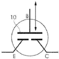
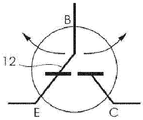
도 1a 및 1b는 각각 종래의 트랜지스터 및 본 발명에 따른 트랜지스터의 기계적 스위치 유사체(mechanical switch analogues)의 동작을 도시하는 개략도이고;
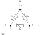
도 2는 본 발명의 예시적 실시형태에 따른 3 단자 트랜지스터의 등가 회로의 모델을 도시하는 개략도이며;
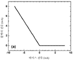
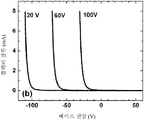
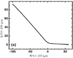
도 3a는 도 2의 모델 트랜지스터 회로에 대응하는 장치의 변환 특성의 그래프로서, 100V의 컬렉터 전위에 있어서 베이스 전류에 대한 컬렉터 전류의 상관성을 도시하고;
도 3b는 동일한 장치의 변환 특성의 그래프로서, 20V, 60V 및 100V의 컬렉터 전위들에 있어서 베이스 전위에 대한 컬렉터 전류의 상관성을 도시하며;
도 4는 본 발명에 따른 트랜지스터의 제 1 예시적 실시형태의 개략도이고;
도 5는 본 발명에 따른 트랜지스터의 제 2 예시적 실시형태의 개략도이며;
도 6은 본 발명에 따른 트랜지스터의 제 3 예시적 실시형태의 개략도이고;
도 7a, 7b 및 7c는 본 발명에 따른 트랜지스터의 제 4 예시적 실시형태의 3개의 변형례들의 개략도이며;
도 8은 본 발명에 따른 트랜지스터의 제 5 예시적 실시형태의 개략도이고;
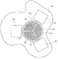
도 9는 도 6에 도시된 제 3 예시적 실시형태에 대응하는 원형 트랜지스터(a prototype version of a transistor)의 사진이며;
도 10 내지 12는 도 9에 도시된 원형 트랜지스터의 변환 기능들을 보여주는 그래프이고;
도 13은 도 7b에 도시된 제 4 예시적 실시형태에 대응하는 원형 트랜지스터의 사진이며;
도 14a 및 14b는 도 13에 도시된 원형 트랜지스터의 변환 기능들을 도시하는 그래프이고;
도 15는 본 발명에 따른 트랜지스터의 제 6 예시적 실시형태의 개략도이다.Figures 1a and 1b are schematic diagrams showing the operation of mechanical switch analogues of conventional transistors and transistors according to the invention, respectively;
2 is a schematic diagram showing a model of an equivalent circuit of a three-terminal transistor according to an exemplary embodiment of the present invention;
FIG. 3A is a graph of the conversion characteristics of the device corresponding to the model transistor circuit of FIG. 2, showing the correlation of the collector current to the base current at a collector potential of 100V;
3B is a graph of the conversion characteristics of the same device, showing the correlation of the collector current to the base potential at 20V, 60V and 100V collector potentials;
Figure 4 is a schematic view of a first exemplary embodiment of a transistor according to the invention;
5 is a schematic view of a second exemplary embodiment of a transistor according to the invention;
Figure 6 is a schematic view of a third exemplary embodiment of a transistor according to the invention;
Figures 7a, 7b and 7c are schematic diagrams of three variants of a fourth exemplary embodiment of a transistor according to the invention;
Figure 8 is a schematic view of a fifth exemplary embodiment of a transistor according to the present invention;
Figure 9 is a photograph of a prototype version of a transistor corresponding to the third exemplary embodiment shown in Figure 6;
Figures 10 to 12 are graphs showing the conversion functions of the circular transistor shown in Figure 9;
13 is a photograph of a circular transistor corresponding to the fourth exemplary embodiment shown in Fig. 7B; Fig.
14A and 14B are graphs showing the conversion functions of the circular transistor shown in FIG. 13;
15 is a schematic diagram of a sixth exemplary embodiment of a transistor according to the present invention.
본 발명은 일종의 전자 장치 및 이러한 전자 장치를 제조하는 방법에 관한 것이다. 구체적으로, 본 발명은, 전자 장치의 제 1 단자를 통한 전류의 방향에 따라, 제 2 단자 및 제 3 단자 중 어느 하나를 통한 전류를 경로설정하는 투-웨이 스위치(two-way switch)로 동작하는 트랜지스터에 관한 것이다. BACKGROUND OF THE INVENTION 1. Field of the Invention The present invention relates to a kind of electronic apparatus and a method of manufacturing such an electronic apparatus. Specifically, the present invention operates with a two-way switch that routes current through either the second terminal or the third terminal, depending on the direction of the current through the first terminal of the electronic device Lt; / RTI >
본 발명은 또한 인쇄, 코팅 및 패키징 기술을 이용한 전자 장치 및 회로의 제조인 인쇄 전자 분야에 관한 것이다. 본 명세서에 있어서, 용어 "인쇄(printing)"는, 다음과 같은, 그러나 이에 한정되지 않는 방법들: 플렉소 인쇄(flexography) 또는 활판 인쇄와 같은 볼록판 인쇄; 그라비어(gravure)와 같은 오목판 인쇄; 패드 인쇄(pad printing) 및 오프셋 리소그래피(offset lithography)를 포함하는 전사법; 리소그래피 및 제로그래피(xerography)와 같은 플랫 인쇄(flat printing) 방법; 스크린 인쇄와 같은 스텐실(stencil) 방법; 및 잉크젯 인쇄와 같은 비접촉 인쇄에 의해 액체 또는 콜로이드 잉크로 기판 물질에 패턴 또는 디자인을 형성하는 것을 의미한다. The present invention also relates to the field of printing electronics, which is the manufacture of electronic devices and circuits using printing, coating and packaging techniques. As used herein, the term "printing" includes but is not limited to the following: but not limited to, flexographic printing such as flexography or letterpress printing; Concave printing such as gravure; Transfer methods including pad printing and offset lithography; Flat printing methods such as lithography and xerography; Stencil methods such as screen printing; And forming a pattern or design on the substrate material with liquid or colloidal ink by non-contact printing, such as inkjet printing.
"코팅(coating)"은 예를 들어 스프레이, 닥터 블레이드(doctor blade), 슬롯-염료(slot-dye) 또는 스핀 코팅(spin coating)에 의해 연속적인 물질 층을 적층하는 것을 의미한다. 이러한 층은 예를 들어 포토리소그래피(photolithography), 기계적 또는 레이저 새김, 또는 에칭에 의해 이후에 패턴화되는 것이 필요할 수 있다. 패키징 기술은, 열간 냉간 적층; 비인쇄 요소 및 부품의 전사; 칼렌더링(calendaring); 스탬핑(stamping); 및 엠보싱(embossing)을 포함하지만 이에 한정되지 않는, 물질의 추가, 제거 및 형성을 위한 인쇄 및 패키징 산업에서 흔하게 발견되는 다른 기술이다. "Coating" means laminating successive layers of material by, for example, spray, doctor blade, slot-dye or spin coating. This layer may need to be patterned later, for example by photolithography, mechanical or laser engraving, or etching. Packaging techniques include hot cold lamination; Transcription of non-printing elements and parts; Calendaring; Stamping; And embossing, which are commonly found in the printing and packaging industries for the addition, removal and formation of materials.
본 명세서에 개시된 트랜지스터는 본질적으로 반도체 물질 및 전기 접점들만으로 이루어져 있고, 공지된 인쇄 또는 박막 적층 기술을 이용하여 2 단계만으로 간단히 제조될 수 있다는 것이 본 발명의 양상이다. 그러므로, 고 전압에서 기능할 수 있는 전류 전환 트랜지스터로서, 특히, 무선 주파수 통신, 및 전계발광 디스플레이와 같은 고 전압 디스플레이 요소를 구동하는 것과 관련된 인쇄 로직의 다른 양상들에 응용할 수 있다. It is an aspect of the present invention that the transistor disclosed herein consists essentially of a semiconductor material and electrical contacts only and can be manufactured simply in two steps using known printing or thin film deposition techniques. Therefore, it can be applied to other aspects of the print logic related to driving a high voltage display element, such as a radio frequency communication, and an electroluminescent display, as a current switching transistor that can function at a high voltage.
본 명세서에 개시된 트랜지스터는, 베이스를 통한 전류가 있을 때 이미터와 컬렉터 사이에 미세 전류가 있다는 점, 및 베이스를 통한 전류의 방향에 따라 이미터와 베이스 사이 또는 베이스와 컬렉터 사이에 전류가 있다는 점에서, 전계 효과 트랜지스터 및 접합 트랜지스터 모두와 다른 동작 원리를 가진다. 비교를 쉽게 하기 위해, 2가지 동작 원리의 기계적 스위치 유사체가 도 1에 도시되어 있다. The transistor disclosed herein has a current between the emitter and the base or between the base and the collector depending on whether there is a microcurrent between the emitter and the collector when there is current through the base and the direction of the current through the base The operation principle is different from that of both the field effect transistor and the junction transistor. For ease of comparison, a mechanical switch analog of two operating principles is shown in Fig.
도 1a 및 1b에는, 각각, 종래의 양극성 접합 트랜지스터 및 본 발명의 트랜지스터에 대한 트랜지스터 동작의 기계적 스위치 유사체가 개략적으로 도시되어 있다. 도 1a에서, 베이스(B)로의 신호 인가는 화살표에 의해 표시된 방향으로 플런저(10)가 선형적으로 움직이는 것과 동등하며, 이에 따라, 이미터(E)와 컬렉터(C) 사이의 연결이 행해지거나 끊어진다. 도 1b에서, 베이스(B)를 통한 전류의 방향 변화는 레버(12)의 회전과 동등하며, 이에 따라, 베이스(B)와 이미터(E) 사이 또는 베이스(B)와 컬렉터(C) 사이의 연결이 행해진다. Figures 1A and 1B schematically illustrate a conventional bipolar junction transistor and a mechanical switch analog of transistor operation for the transistor of the present invention, respectively. 1A, the application of a signal to the base B is equivalent to moving the
따라서, 도 1a에 도시된 동작의 종래의 트랜지스터 모드는 베이스(B)에서의 전류에 의한 전하 주입( 또는 전계 효과 트랜지스터의 게이트에 대한 전위 인가)은 플런저(10)의 수직적 움직임과 동등하여, 이미터(E)와 컬렉터(C) 사이의 연결이 행해지거나 끊어진다. 본 발명에 따른 트랜지스터에서, 베이스를 통한 전류의 방향 변화는 도 1b의 기계적 레버의 회전과 동등하여, 이미터 또는 컬렉터를 베이스와 연결한다. Thus, in the conventional transistor mode of operation shown in FIG. 1A, the charge injection by the current in the base B (or the application of the potential to the gate of the field effect transistor) is equivalent to the vertical movement of the
본 발명의 기본 트랜지스터는 전자 부품 또는 3개 이상의 단자들을 가진 전자 부품들의 조합을 포함하고, 상기 기본 트랜지스터의 등가 회로는 도 2에 도시된 것처럼, 3개의 단자들의 각 쌍을 연결하는 3개의 배리스터들의 3각 네트워크이다. 도 2는, 베이스(B), 이미터(E) 및 컬렉터(C)의 3개의 단자들을 가지며, 3개의 배리스터들(RBE, RCB 및 RCE)로 구성된 트랜지스터의 등가 회로의 모델을 개략적으로 도시한다. The basic transistor of the present invention comprises an electronic component or a combination of electronic components with three or more terminals, and the equivalent circuit of the basic transistor comprises three varistors < RTI ID = 0.0 > 3 each network. 2 shows a model of an equivalent circuit of a transistor having three terminals of a base B, an emitter E and a collector C and consisting of three varistors R BE , R CB and R CE . .
도 2의 전자 장치에서, 1개의 단자와 나머지 2개의 단자들 중 하나 사이의 전류는, 다음과 같은 방식: 양 전류가 제 1 단자에 존재할 때, 즉 제 1 단자로 안쪽을 향하여 흐르는 전류가 존재할 때, 양 전위가 인가되는 제 2 단자를 통한 미세 전류가 있고, 제 2 단자에 대하여 음 전위로 유지되는 제 3 단자로부터의 양 전류가 있으며; 음 전류, 즉 제 1 단자로부터 바깥쪽으로 흐르는 전류가 있을 때, 제 2 단자로의 양 전류 및 제 3 단자를 통한 음 전류가 있는 방식으로 경로설정된다. In the electronic device of Figure 2, the current between one terminal and one of the remaining two terminals is in the following manner: when a positive current is present at the first terminal, i. E. There is a current flowing inward towards the first terminal There is a fine current through a second terminal to which a positive potential is applied and a positive current from a third terminal which is held at a negative potential with respect to the second terminal; When there is a negative current, that is, a current flowing outward from the first terminal, there is a positive current to the second terminal and a negative current through the third terminal.
어느 한 쌍의 단자들 사이의 필요한 배리스터 특성들은, 단자들 사이의 전류 또는 인가된 전위차가 낮을 때 매우 높은 전기 저항을 가지고, 단자들 사이의 전류 또는 인가된 전위가 높을 때 낮은 전기 저항을 가지는 것이다. 전위 Vc가 컬렉터(C)에 인가되고 양 전류 IB가 베이스로 주입될 때, 베이스(B)의 전위(VB)는 이미터(E)에 대하여 큰 양의 값이면서, 컬렉터(C)에 대하여 낮은 값을 가진다. 컬렉터와 이미터를 연결하는 배리스터의 특성들에 대하여 컬렉터 전위(VC)의 크기에 따라, 다른 트랜지스터 유형과 유사하게 오프-전류로서 설명될 수 있는 컬렉터로의 작은 전류가 있을 수 있다. 반대로, 베이스에서의 음 전류, 즉 바깥 방향으로의 전류가 있다면, 베이스 전위(VB)는 컬렉터에 대하여 큰 음의 값을 가지며, 이미터에 대해서는 낮은 값을 가진다. 베이스와 컬렉터를 연결하는 배리스터의 저항 RCB는, 베이스를 이미터에 연결하는 배리스터의 저항 RBE보다 훨씬 낮고, 컬렉터로 흐르는 전류가 가장 많다. The required varistor characteristics between any pair of terminals have a very high electrical resistance when the current between the terminals or the applied potential difference is low and a low electrical resistance when the current between the terminals or the applied potential is high . When the potential V c is applied to the collector C and the positive current I B is injected into the base, the potential V B of the base B is a large positive value with respect to the emitter E, Lt; / RTI > There may be a small current to the collector that can be described as an off-current similar to other transistor types, depending on the magnitude of the collector potential (V C ) for the characteristics of the varistor connecting the collector and emitter. Conversely, if there is a negative current in the base, that is, a current in the outward direction, the base potential (V B ) has a large negative value for the collector and a low value for the emitter. The resistance R CB of the varistor connecting the base and the collector is much lower than the resistance R BE of the varistor connecting the base to the emitter, and the current flowing to the collector is the greatest.
이러한 트랜지스터는 도 2에 도시된 것처럼 함께 연결된 3개의 개별적인 배리스터들로 간단히 구성될 수 있고, 이러한 배리스터들은 전자 부품 제조 분야에서 공지된 적합한 방법에 따라 단지 3개의 단자들 또는 연결 리드들을 가진 통상의 하우징으로 함께 패키징될 수 있다. 선택적으로, 트랜지스터는, 집적 회로 제조, 박막 전자, 또는 인쇄 전자에 통상적으로 적용되는 물질의 적층 및 패터닝에 대한 기술을 이용하여, 통상의 기판 상에 적어도 3개의 개별적 배리스터들의 집적 회로로 형성될 수 있다. These transistors may simply be constructed of three individual varistors connected together as shown in Fig. 2, and these varistors may be connected to a common housing with only three terminals or connection leads in accordance with a suitable method known in the manufacture of electronic components Can be packaged together. Alternatively, the transistor may be formed of an integrated circuit of at least three individual varistors on a conventional substrate, using techniques for stacking and patterning materials commonly applied to integrated circuit fabrication, thin film electronics, or printing electronics have.
그러나, 트랜지스터 자체는 가능한한 적은 단계들로 제조된 단일의 전자 부품만을 포함하는 것이 바람직하다. 그러므로, 본 발명의 바람직한 실시형태에 따르면, 적어도 반도체 물질 및 단자들을 형성하는 적어도 3개의 도전성 접점들을 포함하는 전자 부품이 제조되고, 다음과 같은 방식: 제 1 단자로의 양 전류가 있을 때, 양 전위가 인가되는 제 2 단자를 통한 미세 전류, 및 제 2 단자에 대하여 음 전위로 유지되는 제 3 단자로부터의 양 전류가 있고; 제 1 단자에서의 음 전류, 즉 제 1 단자의 바깥쪽으로의 전류가 있을 때, 제 2 단자로의 양 전류 및 제 3 단자를 통한 미세 전류가 있다. However, the transistor itself preferably includes only a single electronic component fabricated in as few steps as possible. Therefore, according to a preferred embodiment of the present invention, an electronic component is manufactured which comprises at least three conductive contacts forming at least a semiconductor material and terminals, in the following manner: when there is a positive current to the first terminal, There is a fine current through a second terminal to which a potential is applied and a positive current from a third terminal which is held at a negative potential with respect to the second terminal; When there is negative current at the first terminal, that is, current to the outside of the first terminal, there is a positive current to the second terminal and a fine current through the third terminal.
배리스터 특성들은 반도체 물질과 접점들을 형성하는 물질 사이의 동일한 정류 접합들의 존재로부터 생길 수 있다. The varistor characteristics can arise from the presence of the same rectifying junctions between the semiconductor material and the material forming the contacts.
또 다른 실시형태에서, 배리스터 특성들은, 반도체 물질이 미립자 또는 미세 입자형 재료임에 따라, 반도체 접합이 입자들 사이의 계면을 형성하는 반도체 물질에서의 다수의 대칭 반도체 접합들로부터 생겨난다. In yet another embodiment, the varistor characteristics arise from a plurality of symmetric semiconductor junctions in a semiconductor material, wherein the semiconductor junction forms an interface between the particles, as the semiconductor material is a particulate or microparticulate material.
또 다른 실시형태에서, 배리스터 특성들은, 반도체 물질이 적어도 2개의 전기적으로 상이한 물질들을 포함하는 합성물임에 따라, 다수의 무작위로 배향되거나 대향하는 정류 접합들이 상기 2개의 전기적으로 상이한 물질들 사이의 계면을 형성하는 상기 반도체 물질에서의 상기 정류 접합들로부터 생겨난다. In yet another embodiment, the varistor characteristics are such that as the semiconductor material is a composite comprising at least two electrically different materials, a plurality of randomly oriented or opposing rectifying junctions are formed between the two electrically different materials Lt; RTI ID = 0.0 > semiconductor material < / RTI >
반도체 물질은, 일면에 배치된 2개 이상의 단자들 및 타면에 배치된 1개 이상의 단자를 갖는 플레이트, 층 또는 디스크의 형태를 가질 수 있다. The semiconductor material may have the form of a plate, layer or disk having two or more terminals disposed on one side and one or more terminals disposed on the other side.
한 쌍의 단자들 사이의 원하는 배리스터 특성들을 달성하는 2개의 방법들이 문헌에 공지되어 있다. 첫번째 방법은, 반도체 물질과 접점들을 형성하는 물질 사이의 동일한 정류 접합들을 구성하여, 어느 2개의 단자들 사이의 경로가 한 쌍의 동일하지만 대향하는 다이오드를 포함하는 것이다. 이러한 정류 접합은, 접점의 도전성 물질과 반도체 물질 사이의 계면을 포함하는 쇼트키 장벽(Schottky barrier)의 형태를 가질 수 있다. 선택적으로, 정류 접합은, 일종의 도전성을 가진 반도체 물질과 반대되는 도전성을 가진 또 다른 고 첨가 반도체 사이의 반도체 접합일 수 있고, 상기 고 첨가 반도체는 전기적 연결에 필요한 도전성 물질과 옴 접촉을 행한다. Two methods of achieving desired varistor characteristics between a pair of terminals are known in the literature. The first method is to construct the same rectifying junctions between the semiconductor material and the materials that form the contacts so that the path between any two terminals includes a pair of identical but opposing diodes. Such a rectifying junction may have the form of a Schottky barrier including an interface between the conductive material of the contact and the semiconductor material. Optionally, the rectifying junction may be a semiconductor junction between a semiconductor material having a conductivity type and another high-doped semiconductor having conductivity opposite to the conductivity type, and the high-doped semiconductor makes ohmic contact with the conductive material necessary for electrical connection.
두번째 바람직한 방법은, 고유 전계 또는 전류 의존 도전성을 가지고, 이에 따라 배리스터 물질로 설명되는 반도체 물질을 사용하는 것이다. 이러한 방법의 장점은, 자유 전하를 안내한다면, 더 이상 정류 접합을 제공할 필요가 없기 때문에, 접점 및 전기적 연결을 위한 물질을 자유롭게 선택할 수 있다는 것이다. 이러한 물질의 예가 고시 등(Ghosh et al)의 WO 2012/027109, 홍 등(Hong et al)의 US 2012/0153237, 및 쉬 등(Shi et al)의 WO 2012/071051에 개시되어 있다. A second preferred method is to use a semiconductor material that has a high electric field or current-dependent conductivity and is thus described as a varistor material. An advantage of this method is that if the free charge is guided, there is no need to provide a rectifying junction anymore, so that the material for the contacts and the electrical connection can be freely selected. Examples of such materials are disclosed in WO 2012/027109 of Ghosh et al., US 2012/0153237 of Hong et al, and WO 2012/071051 of Shi et al.
이러한 물질들 중 대부분은 적어도 2개의 전기적으로 상이한 물질들을 포함하는 합성물이고, 배리스터 특성들은, 상기 2개의 전기적으로 상이한 물질들 사이의 계면에 형성되는 반도체 물질에서의 다수의 무작위로 배향되거나 대향하는 정류 접합들로부터 생겨난다. 선택적으로, WO 2007/0004014에 개시된 바와 같이, 실리콘 나노 입자로 구성된 단상 물질이 제공되며, 상기 단상 물질은, WO 2012/035494에서, 서미스터와 같이 응용에 적합한 우수한 배리스터 특성들을 가진다는 것이 밝혀졌다. Most of these materials are composites comprising at least two electrically different materials and the varistor characteristics include a number of randomly oriented or opposing rectification in the semiconductor material formed at the interface between the two electrically different materials It arises from junctions. Alternatively, as disclosed in WO 2007/0004014, there is provided a single-phase material consisting of silicon nanoparticles, said single phase material being found in WO 2012/035494 to have excellent varistor characteristics suitable for applications such as thermistors.
본 발명의 제 1 예시적 실시형태는, 도 2에 도시된 회로와 관련하여, TDK EPCOS에서 제조된 SIOV-S14K75 유형의 3개의 개별적인 배리스터들을 이용하여 구성된 모델 회로이다. 회로는, 베이스(B), 이미터(E) 및 컬렉터(C)로 표시된 3개의 단자들을 가진다. 컬렉터 전류(IC)에 대한 측정된 변환 특성들은, 도 3a에서는, 100V의 컬렉터 전위에 대한 베이스 전류(IB)의 함수로서 도시되고, 도 3b에서는, 20V, 60V 및 100V의 컬렉터 전위들에 대한 베이스 전압(VB)의 함수로서 도시된다. 전류-전류 변환 특성은, 음의 베이스 전류에 대해 1보다 약간 작은 음의 경사의 선형 반응을 가지며, 양의 베이스 전류에 대해 낮은 오프-전류를 가진 거의 완벽한 전환 행위를 보여준다. 또한, 도 3b에 도시된 바와 같이, 전류가 변환되는 명확한 베이스 전위가 있으며, 이러한 스위치-온 전압은 컬렉터에 인가된 전위에 의존한다. 따라서, 이러한 구성의 장치는, 근사적인 단일 이득 증폭기/감쇠기로서 또는 인버터로서 사용될 수 있다. 추가적인 응용예들은 컬렉터로의 음 신호와 이미터로의 양 신호를 분리함으로써 가능한 정류, 필터링 및 신호 처리를 포함한다. A first exemplary embodiment of the present invention is a model circuit constructed using three separate varistors of the SIOV-S14K75 type fabricated in TDK EPCOS with respect to the circuit shown in Fig. The circuit has three terminals denoted as base (B), emitter (E) and collector (C). The measured conversion characteristics for the collector current I C are shown as a function of the base current I B for a collector potential of 100 V in Figure 3A and are shown as a function of the collector potentials of 20 V, 60 V and 100 V in Figure 3B Is shown as a function of the base voltage (V B ). The current-to-current conversion characteristic has a linear response with a negative slope of slightly less than 1 for negative base current, and shows a nearly perfect conversion behavior with low off-current for a positive base current. Also, as shown in FIG. 3B, there is a definite base potential at which the current is converted, and this switch-on voltage depends on the potential applied to the collector. Thus, a device of this configuration can be used as an approximate single gain amplifier / attenuator or as an inverter. Additional applications include possible rectification, filtering, and signal processing by separating the negative signal to the collector and both signals to the emitter.
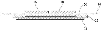
본 발명의 제 2 실시형태는, 반도체 물질의 몸체 및 베이스, 이미터 및 컬렉터 단자를 형성하는 적어도 3개의 도전성 접점들을 포함하는 개별적인 부품으로서의 단일체 구성의 트랜지스터이다. 예시적으로, 2개의 가능한 구성들이 도 4 및 5에 도시되어 있다. A second embodiment of the present invention is a monolithic transistor as a discrete component comprising at least three conductive contacts forming the body and base, emitter and collector terminals of a semiconductor material. Illustratively, two possible configurations are shown in Figures 4 and 5.
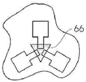
도 4의 경우, 반도체 몸체(14)는 플레이트 또는 디스크 또는 물질 층의 형태를 가진 평판을 포함한다. 이격되게 인접한 이미터 단자(16) 및 컬렉터 단자(18)는 반도체 몸체(14)의 상면에 형성되어 있고, 베이스 단자(20)는 반도체 몸체의 반대측 하면에 형성되어 있다. 도시된 것처럼, 몸체(14)는 접점들에 의해 점유된 영역을 넘어 연장될 수 있다. In the case of FIG. 4, the
베이스 접점(20)은 서로 인접한 이미터 접점(16)과 컬렉터 접점(18)으로부터 몸체의 반대측 면에 있기 때문에, 베이스와, 컬렉터 또는 이미터 사이에서 정의된 배리스터들을 포함하는 경로는 몸체의 두께를 지나고, 이에 반하여, 컬렉터와 이미터 사이의 경로는 몸체의 상면에 가까운 횡 방향이 된다. 따라서, 이러한 구조는, 자동적으로, 동일한 전위 차에 있어서, 이미터와 컬렉터 사이의 저항이 이미터 또는 컬렉터와 베이스 사이의 저항보다 확실히 높아지게 하고, 상대적으로 작은 오프-전류를 보장한다. Since the
베이스 접점(20)을 덮는 절연층(22)은 몸체(14)의 하면에 형성되고, 추가 도전성 접점(24)은 절연층의 노출면에 형성된다. 이러한 접점(24)은 트랜지스터에 대한 몸체 또는 접지 단자를 제공하는 역할을 한다. An insulating
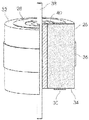
도 5에 도시된 제 2 실시형태의 선택적인 구성은, 실린더 또는 정각 기둥의 형태를 가진 반도체 물질의 몸체(26), 상기 몸체의 각각의 대향하는 말단면들(32, 34)에 배치된 대향하는 환형의 이미터 단자(28)와 컬렉터 단자(30), 및 2개의 상기 말단면들을 연결하는 원통면에 배치된 적어도 1개의 베이스 단자(36)을 포함한다. 베이스 단자(36)는 도 5에 도시된 바와 같이 몸체(26)를 완전히 둥글게 감싸는 단일의 원주형 접점을 포함할 수도 있고, 몸체의 표면 중 서로 다른 위치들에 분포된 2개 이상의 개별적인 접점들을 포함할 수도 있다. The alternative configuration of the second embodiment shown in Fig. 5 comprises a
몸체(26)를 통하여 축방향으로 연장되는 보조 접점(38)은 동축 슬리브 또는 원통(40)에 의해 몸체의 반도체 물질로부터 분리되고, 몸체 또는 접지 단자로서 사용가능한 도 4의 접점(24)과 동등하다. The
접지 단자는 전자 장치를 완전히 둘러쌈으로써 하우징을 형성하도록 구성되거나, 또는 선택적으로, 예를 들면 도 4에 도시된 하면의 도전성 층 또는 접점(24) 또는 도 5에 도시된 도전성 동축 코어(38)와 같은 추가적인 특징으로 형성될 수 있다. The ground terminal may be configured to form the housing by completely enclosing the electronic device, or alternatively may be configured to form a housing, e.g., a conductive layer or contact 24 of the lower surface shown in FIG. 4 or the conductive
본 발명의 바람직한 실시형태들은 제한된 개수의 단계로 기판에 인쇄 공정 또는 박막 적층 공정에 의해 제조될 수 있다. 일반적으로, 이러한 제조는, 동시에 배치되고, 반도체 층의 동일면 상에 배치된 이미터 접점, 베이스 접점 및 컬렉터 접점을 위한 물질을 가진 동일면 구조의 접점들의 채택을 암시한다. 그러나, 특별한 응용의 경우, 예를 들면, 고 전류가 필요한 경우, 도 4에 도시된 구조와 유사한 엇갈리거나 대향하는 구조를 채택하는 것이 바람직할 수 있으며, 절연 층(22)은 폴리머 박막과 같은 절연성 물질 또는 종이 또는 직물과 같은 섬유상 물질로 구성된 기판을 포함하거나, 또는 접지 단자(24)는 금속 호일(metal foil)과 같은 도전성 물질로 구성된 기판을 포함한다. Preferred embodiments of the present invention can be produced by a printing process or a thin film deposition process on a substrate in a limited number of steps. Generally, this manufacturing implies the adoption of co-planar contacts having materials for emitter, base and collector contacts arranged at the same time and disposed on the same side of the semiconductor layer. However, for special applications, for example, where high current is required, it may be desirable to employ a staggered or opposing structure similar to that shown in FIG. 4, Or a substrate made of a fibrous material such as paper or cloth, or the
도 6은, 도전성 접점들이 동일면 구조로 배치되고, 인쇄에 의해 바람직하게 제조된 본 발명의 제 3 예시적 실시형태를 도시한다. 이러한 실시형태에서, 절연성 물질로 구성되는 비도전성 표면을 가진 기판(42)이 제공되거나, 선택적으로, 전자 장치가 제조되는 표면의 적어도 일부분을 덮는 절연성 물질 층을 가진 도전성 또는 반도체 물질이 제공된다. Figure 6 shows a third exemplary embodiment of the present invention in which the conductive contacts are arranged in a coplanar configuration and are preferably produced by printing. In this embodiment, a
전자 장치의 관점에서, 적층 방법 이용 및 응용 분야에 적합해야 한다는 것을 제외하고는, 기판 물질 또는 기판의 크기의 선택에 제한은 없다. 이상적으로, 인쇄 전자 분야에서 예상되는 응용에 있어서, 기판 물질은, 연속적인 박막, 직물 또는 비직물 섬유상 물질, 또는 연속적인 박막과 섬유상 물질의 복합물일 수 있는 가요성 또는 견고한 시트 물질이다. There is no restriction on the choice of the size of the substrate material or the substrate, except in terms of electronic devices, which should be suitable for lamination method applications and applications. Ideally, for applications expected in the printed electronics field, the substrate material is a flexible or rigid sheet material that can be a continuous thin film, woven or nonwoven fibrous material, or a composite of continuous thin film and fibrous material.
박막 물질의 예는 다음과 같다: 폴리에틸렌 테레프탈레이트(polyethylene terephthalate; PET), 폴리에틸렌(polyethylene; PE), 폴리카보네이트, 폴리에틸렌 나프탈레이트(polyethylene napthalate; PEN), 폴리이미드 (켑톤(kapton), 베스펠(vespel)), 셀룰로오스 아세테이트 및 셀룰로오스 아세테이트 뷰티레이트(cellulose acetate butyrate; CAB)와 같은 셀룰로오스 유도체, 및 페놀 및 알킬 에폭시 수지를 포함하지만 이에 한정되지 않는 폴리머들; 및 강철 및 스테인리스 스틸 합금과 같은 철 금속, 구리 및 구리 합금, 알루미늄 및 알루미늄 합금, 티타늄 및 티타늄 합금, 및 마그네슘 및 마그네슘 합금을 포함하지만 이에 한정되지 않는 금속. Examples of thin film materials are as follows: polyethylene terephthalate (PET), polyethylene (PE), polycarbonate, polyethylene naphthalate (PEN), polyimide (kapton, vespel), cellulose derivatives such as cellulose acetate and cellulose acetate butyrate (CAB), and polymers including, but not limited to, phenols and alkyl epoxy resins; And metals such as but not limited to ferrous metals such as steel and stainless steel alloys, copper and copper alloys, aluminum and aluminum alloys, titanium and titanium alloys, and magnesium and magnesium alloys.
섬유상 물질은 다음을 포함한다: 합성 섬유, 및 식물, 채소, 광물, 울, 면, 리넨, 또는 스톤 울(stone wool; 락 울(rock wool))과 같은 천연 섬유의 직물 및 비직물 섬유; 식물 섬유로부터 제조된 전통적 종이 및 보드, 및 듀퐁 노멕스(Du Pont Nomex)와 같은 아라미드 종이(aramid paper) 및 세라믹 종이와 같은 종이 유사 물질. Fibrous materials include: synthetic and nonwoven fabrics of natural fibers such as plants, vegetables, minerals, wool, cotton, linen, or stone wool (rock wool); Traditional paper and boards made from plant fibers, and paper-like materials such as aramid paper and ceramic paper such as Du Pont Nomex.
복합 기판 물질은 다음을 포함한다: 임의의 물질로 이루어진 나노입자, 나노튜브, 나노와이어, 나노로드(nanorod) 및 삽입 나노클레이(intercalated nanoclay)와 같은 나노스케일 필러(filler)를 가진 것들을 포함하지만 이에 제한되지 않는 섬유 및 입자 강화 폴리머 및 금속; 목재와 같은 천연 물질; 수퍼우드(superwood) 또는 칩보드(chipboard)와 같은 재구성 목재; 적층 시트; 및 적어도 하나의 표면에 형성된 연속적이거나 텍스쳐 코팅을 가진 박막 또는 섬유상 시트. Composite substrate materials include those with nanoscale fillers such as nanoparticles of any material, nanotubes, nanowires, nanorods and intercalated nanoclay, Fiber and particle reinforced polymers and metals; Natural materials such as wood; Reconstructed wood such as superwood or chipboard; A laminated sheet; And a thin film or fibrous sheet having a continuous or textured coating formed on at least one surface.
박막 적층 또는 마이크로 전자기술 제조와 같은 다른 응용 또는 제조 공정에 있어서, 기판 물질은 또한 결정 또는 비결정 산화물, 나트륨 유리, 붕규산 유리, 석영, 티탄산 바륨 또는 사파이어와 같은 규산염 및 티탄산염, 또는 실리콘, 게르마늄을 포함하고 이에 한정되지 않는 반도체, 또는 갈륨 아세나이드(gallium arsenide), 인화인듐 또는 셀렌화 인듐 구리와 같은 화합물 반도체를 포함할 수 있다. In other applications or fabrication processes such as thin film deposition or microelectronic fabrication, the substrate material may also include silicates and titanates, such as crystalline or amorphous oxides, sodium glass, borosilicate glass, quartz, barium titanate or sapphire, or silicon, germanium But are not limited to, semiconductors, or compound semiconductors such as gallium arsenide, indium phosphide, or indium selenide copper.
위의 예들은 제한하려는 의도를 가지고 있는 것은 아니다. The above examples are not intended to be limiting.
베이스, 이미터, 및 컬렉터를 위한 도전성 접점들은 기판(42)의 절연층 상에 적층되고, 베이스를 정의하는 2개의 대향하는 전기 접점들(42, 46)이 각각, 이미터 및 컬렉터를 위한 접점들(50, 52)을 분리하는 좁게 연장된 갭(gap; 48)의 대향하는 말단들에 배치되는 패턴으로 형성된다. 2개의 베이스 접점(44, 46)은 컬렉터 접점(52)을 감싸는 도전성 물질의 경로(54)에 의해 연결된다. 베이스 접점들(44, 46)은 갭(48)의 길이를 결정하는 3각형 모양으로 테이퍼(taper)된 끝을 가진다는 것을 도 6으로부터 알 수 있다. 도시된 전자 장치의 구성은 이미터와 컬렉터에 대해 대칭을 이루므로, 이미터와 컬렉터는 자유롭게 서로 교환될 수 있다. The conductive contacts for the base, emitter, and collector are stacked on an insulating layer of the
접점들을 정의하는 도전성 물질의 적층 및 패터닝은, 예를 들어, 도전성 잉크의 인쇄에 의해, 또는 마스크를 통한 물리적 또는 화학적 증착에 의해 동일한 처리 단계에서 일어나야 한다. 인쇄 장치의 경우, 접점에 적합한 물질들은, 마이크로범위 또는 나누구조 형태일 수 있는 금속 또는 탄소를 함유하는 잉크들이지만, 인듐, 주석, 아연 및 안티모니의 산화물들과 같은 다른 도전성 물질들, 또는 PEDOT:PPS와 같은 유기 도체들을 함유하는 잉크들이 동등하게 적용될 수 있다. 반도체 물질이 박막 적층에 의해 적층될 장치의 경우, 금속의 선택은, 정류 접합에 반도체를 제공하는 데에 필요한 조합에 의해 제한될 수 있다. 따라서, 일반적으로, 몰리브덴, 팔라듐, 티타늄, 텅스텐, 니켈 또는 이들의 합금을 포함하는 높은 일 함수 금속, 또는 은, 구리 도는 주석과 같은 중간 일 함수를 가진 금속 및 합금이 바람직할 수 있다. The deposition and patterning of the conductive material defining the contacts should take place in the same processing step, for example, by printing of the conductive ink, or by physical or chemical deposition through a mask. In the case of printing devices, materials suitable for the contacts are metals or carbon-containing inks which may be in the micro-range or in the form of a split structure, but other conductive materials such as oxides of indium, tin, zinc and antimony, : Inks containing organic conductors such as PPS are equally applicable. In the case of a device in which a semiconductor material is to be deposited by thin film deposition, the choice of metal may be limited by the combination required to provide the semiconductor for rectifying junction. Thus, in general, high work function metals, including molybdenum, palladium, titanium, tungsten, nickel or alloys thereof, or metals and alloys having an intermediate work function such as silver, copper or tin may be preferred.
그 다음에, 반도체 몸체(56)는 적층되고 패턴화되어, 4개의 접점들(44, 46, 50 및 52) 사이의 갭을 덮으며, 베이스 접점들을 통하여 연장되는 갭(48)의 축을 중심으로 거울 대칭을 가진다. 반도체 몸체(56)는, 갭(48)에 인접한 접점들의 가장 안쪽에 있는 말단들과 오버랩되기에 충분히 크다. The
점접들을 덮는 반도체 물질의 면적은 전기적 특성에 영향이 없고, 이러한 디자인에 대한 대안에서 도체 물질에 의해 분로되기 때문에, 반도체 물질은, 도체들 사이의 5개의 갭들 각각(즉, 이미터와 베이스 (상단), 컬렉터와 베이스 (상단), 이미터와 베이스 (하단), 컬렉터와 베이스 (하단), 및 이미터와 컬렉터)을 브릿지(bridge)하는 5개의 트랙(track)들을 포함하는 패턴으로 제한될 수 있다. 반도체 몸체의 적층 및 패터닝은, 예를 들어 반도체 잉크의 인쇄에 의해 또는 마스크를 통한 물리적 또는 화학적 증착에 의해 단일 단계로 행해지는 것이 바람직하다. Since the area of the semiconductor material covering the gaps does not affect the electrical properties and is shunted by the conductor material in an alternative to this design, the semiconductor material can be electrically connected to each of the five gaps between the conductors (i.e., ), Five tracks that bridge the collector and base (top), emitter and base (bottom), collector and base (bottom), and emitter and collector) have. The stacking and patterning of the semiconductor body is preferably performed in a single step, for example by printing of a semiconductor ink or by physical or chemical deposition through a mask.
인쇄 장치에서, 건조 또는 경화로 배리스터 물질을 형성하는 잉크는, 인쇄 장치의 도전성 부분들에 대한 물질의 선택에 제한을 두지 않기 때문에, 동종의 반도체들을 형성하는 것들을 이용하는 것이 바람직하다. 바람직한 물질은, WO 2007/0004014에 개시된 특정 표면 특성들을 가진 나노 입자들이거나, WO 2012/035494에 개시된 서미스터에서의 사용을 통해 배리스터 물질을 형성하는 것으로 증명된 실리콘 입자를 포함하는 잉크이다. P3HT 또는 PEDOT와 같은 유기 반도체 물질은, 통상적인 배리스터 물질이 아닐지라도, 일반적으로 가장 흔한 금속들과 정류 접합을 형성하기 때문에 선택적으로 사용될 수 있다. In the printing apparatus, it is preferable to use those which form homogeneous semiconductors, since the ink which forms the varistor material by drying or curing does not restrict the selection of the material for the conductive parts of the printing apparatus. Preferred materials are nanoparticles having specific surface properties disclosed in WO 2007/0004014 or inks comprising silicon particles which have been proven to form varistor materials through use in thermistors as disclosed in WO < RTI ID = 0.0 > Organic semiconductor materials, such as P3HT or PEDOT, can be used selectively because they form a rectifying junction with generally the most common metals, although not a conventional varistor material.
선택적인 공정에 있어서, 적층의 순서가 뒤바뀌어, 반도체 몸체가 먼저 기판 상에 적층되고 최종 구성에서 단자와 기판 사이에 배치될 수도 있다. In an optional process, the stacking order is reversed so that the semiconductor body may first be stacked on the substrate and disposed between the terminal and the substrate in the final configuration.
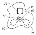
절연면을 가진 기판 물질에 인쇄, 박막 적층 또는 통상의 반도체 제조 기술에 의해 제조될 수 있는 본 발명의 제 4 예시적 실시형태는, 반도체 몸체와 접촉하고 대칭 패턴으로 배열된 3개의 단자들만을 포함한다. 본 실시형태는, 베이스 단자들(44, 46) 사이에서 연장되는 도체(54)가 중앙 컬렉터 단자(52)로의 접근을 제한한다는 점에서, 도 6의 실시형태를 하나의 회로로 집적하는 데에 어려움을 인식하였다. 결과적으로, 예를 들어 절연성 물질 및 도전성 물질을 적층함으로써 비어를 형성하는 적어도 2개의 추가 처리 단계들이 회로를 완성하는 데에 필요하다. 제 4 실시형태에서, 기판 면으로의 접근이 모든 단자들에 개방되고, 전기적 연결이 단자로서 동일한 처리 단계에서 행해지는 것을 가능하게 한다. 본 실시형태의 3개의 디자인 실시예들은, 각각 적절한 대칭을 가지면서, 도 7a, 7b 및 7c에 도시되어 있다. A fourth exemplary embodiment of the present invention, which may be produced by printing, thin-film deposition or conventional semiconductor fabrication techniques on a substrate material having an insulating surface, comprises only three terminals in contact with the semiconductor body and arranged in a symmetrical pattern do. This embodiment differs from the embodiment shown in Fig. 6 in that the
베이스, 이미터 및 컬렉터로서 사용되는 3개의 대칭 배열 전기 접점들(58, 60, 62)은 기판(64)에 적층되고 패턴화된다. 한편, 사용되는 물질 및 공정은 도 6에 도시된 실시형태와 동일하다. 그 다음에, 반도체 몸체(66)는, 단자들(58, 60, 62)의 인접한 안쪽 말단들 사이에 정의된 3각형 갭(68) 위에, 3개의 단자들을 동일하게 연결하는 3회 회전 대칭을 가진 디자인으로 적층되고 패턴화된다. The three symmetrical array
적층된 반도체 물질(66)의 바람직한 모양들은, 도 7a, 7b 및 7c에 각각 도시된 바와 같이, 원, 접점들의 안쪽 말단들을 지나 연장되고 전기적 접촉을 행하는 변들을 가진 정삼각형, 및 접점들의 안쪽 말단들을 지나 연장되는 꼭지점들을 가진 정삼각형이다. 이전의 실시형태와 같이, 반도체 물질의 고체 층 또는 시트를 포함하는 몸체(66)는, 단자들 사이의 정확한 방향과 위치에서 만곡형 또는 직선형 트랙들에 의해 대체될 수 있다. 반도체 물질의 선택 및 제조 방법은 이전의 실시형태와 동일하며, 도체 및 반도체 물질을 적층하는 순서는 바뀔 수 있다. The preferred shapes of the stacked
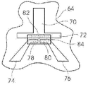
도 7a 내지 7c에 도시된 제 4 실시형태의 대칭 디자인은 각 쌍의 단자들 사이의 저항의 변화를 가능하게 하도록 변화될 수 있지만, 디자인에 있어서 제한된 유연성을 가진다. 이전의 2개의 실시형태들과 동일한 물질들 및 공정들을 이용하여 제조될 수 있는 제 5 실시형태는 이러한 파라미터들을 더욱 정밀하게 제어할 수 있게 한다. 도 8에 도시된 이러한 실시형태에서, 베이스(70)는 T의 머리(72)가 연장된 T 모양을 가진다. 이미터 및 컬렉터 접점들(74, 76)은, 베이스 단자의 머리(72)와 인접하게 배치되고, 서로 인접하게 대칭적으로 배치되는 안쪽으로 연장된 직사각형 말단부들(78, 80)을 가지며, 각각의 말단부(78, 80)의 한쪽 가장자리는 베이스 단자의 인접한 가장자리와 평행하고, 이미터 및 컬렉터 말단부들의 대향하는 가장자리들은 갭을 사이에 두고 서로 평행하게 연장한다. 종합적으로, T 모양 갭(82)이 각각의 접점들 사이에 존재한다. The symmetrical design of the fourth embodiment shown in Figs. 7a to 7c can be varied to enable a change of resistance between each pair of terminals, but has limited flexibility in design. A fifth embodiment, which may be fabricated using the same materials and processes as the previous two embodiments, allows for more precise control of these parameters. In this embodiment shown in Fig. 8, the
기생 저항 및 부유 용량을 최소화하기 위해, 이미터 및 컬렉터 접점들의 바깥쪽 단자부들(74, 76)은 서로 멀어지는 각도로 연장된다. 반도체 몸체(84)가 3개의 갭들을 덮도록 적층된 이후에, 등가 회로의 배리스터들의 상대 저항들은 이미터 및 컬렉터 접점들의 말단부들(78, 80)의 길이들 및 각 쌍의 접점들 사이의 갭의 길이에 의해서만 결정된다. 따라서, 이러한 디자인은 이미터-베이스, 베이스-컬렉터 및 이미터-컬렉터 채널들에 대해 비대칭 저항 값들을 가능하게 한다. To minimize parasitic resistance and stray capacitance, the outer
실시예들Examples
도 9는 도체 잉크 및 반도체 잉크의 스크린 인쇄에 의해 제조된 제 3 실시형태(도 6)의 원형 트랜지스터의 사진을 도시한다. 기판은 제곱미터 당 90 그램 중량의 비코팅 백상지를 포함한다. 본 실시형태의 다른 실시예들이 또한 160 gsm 비코팅 종이 보드 상에 제조되고, 100 마이크론 PET 상에 제조되었다. Fig. 9 shows a photograph of a circular transistor of the third embodiment (Fig. 6) produced by screen printing of conductive ink and semiconductor ink. The substrate includes an uncoated backing paper weighing 90 grams per square meter. Other embodiments of this embodiment were also fabricated on a 160 gsm uncoated paper board and made on 100 micron PET.
전자 장치의 접점들 및 다른 도체 부분들은 듀퐁 룩스프린트 5000 은 도체(Du Pont Luxprint 5000 silver conductor)를 이용하여 인쇄된다. 접점들이 크리에이티브 머티리얼즈(Creative Materials Inc.) 및 피켐(PChem Inc.)을 포함한 다른 제조자들로부터 얻어진 은 및 은 합금 잉크; 및 반도체 물질에 일정한 전계 독립 저항을 제공하는 듀퐁 7162 룩스프린트 반투명 도체를 이용하여 인쇄된 유사한 장치들이 제조되었다. Contacts and other conductor portions of the electronic device are printed using a Du Pont Luxprint 5000 silver conductor from DuPont Luxx Print 5000. Silver and silver alloy inks where the contacts are obtained from other manufacturers including Creative Materials Inc. and PChem Inc.; And similar devices printed using a DuPont 7162 Lux Print translucent conductor that provides a constant field-independent resistance to the semiconductor material.
반도체 패턴은 실리콘 나노입자 및 아크릴 바인더를 포함하는 잉크를 이용하여 인쇄되었다. 이용된 실리콘 나노입자는 WO 2007/0004014에 개시된 유형이었으며, 실트로닉스(Siltronix)에 의해 제공된 0.005 Ωcm 보다 낮은 저항의 붕소 도핑 p 타입 실리콘 공급원료로부터 WO 2009/125370에 개시된 밀링 방법을 이용하여 제조되었다. 이용된 다른 잉크들은, 실트로닉스에 의해 제공된 유사한 저항을 가진 n 타입 실리콘 공급원료, 및 실리콘 스멜터즈(Silicon Smelters (Pty) Ltd.)에 의해 제공된 2503 등급 실리콘 금속으로부터 준비되었다. Semiconductor patterns were printed using inks containing silicon nanoparticles and acrylic binders. The silicon nanoparticles used were of the type disclosed in WO 2007/0004014 and were prepared using the milling method disclosed in WO 2009/125370 from a boron doped p-type silicon feedstock of resistance lower than 0.005 Ωcm provided by Siltronix . Other inks used were prepared from n-type silicon feedstock with similar resistance provided by Siltronic, and 2503 grade silicone metal provided by Silicon Smelters (Pty) Ltd.
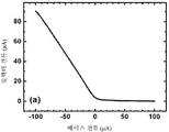
도 10 및 11은, p 및 n 타입 실리콘 나노입자들을 포함하는 잉크 및 은 접점들을 이용하여 인쇄된 본 실시형태의 트랜지스터들의 변환 특성들을 도시하고, 도 10a에서는 베이스 전류에 대한 컬렉터 전류의 의존성이 도시되며, 도 10b에서는 베이스 전압에 대한 컬렉터 전류의 의존성이 도시된다. 도 11에서는, 등가 회로에서의 3개의 배리스터들 각각을 지나는 (즉, 각 쌍의 단자들 사이의) 전위차들에 대한 컬렉터 전류를 묘사하는 모델 함수로의 피트(fit)가 도시된다. Figures 10 and 11 illustrate the conversion characteristics of the transistors of this embodiment printed using ink and silver contacts comprising p and n type silicon nanoparticles where the dependence of the collector current on the base current is shown in Figure 10A, And the dependence of the collector current on the base voltage is shown in Fig. 10B. In FIG. 11, a fit to a model function is depicted that depicts the collector current for potential differences across each of the three varistors in the equivalent circuit (i. E., Between each pair of terminals).
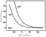
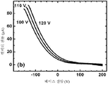
더욱 구체적으로, 도 10은, 평면 종이 기판에 은 접점들 및 p 타입 실리콘 반도체를 스크린 인쇄함으로써 제조된 제 3 실시형태에 따른 트랜지스터의 변환 특성을 도시하고, 100V의 컬렉터 전위에 있어서 베이스 전류에 대한 컬렉터 전류의 의존성(도 10a) 및 80V 및 120V의 컬렉터 전위에 있어서 베이스 전위에 대한 컬렉터 전류의 의존성(도 10b)을 보여준다. More specifically, Fig. 10 shows the conversion characteristics of the transistor according to the third embodiment produced by screen printing the silver contacts and the p-type silicon semiconductor on a flat paper substrate, and shows the conversion characteristics for the base current at a collector potential of 100 V 10A) and the dependence of the collector current on the base potential at collector potentials of 80V and 120V (FIG. 10B).
도 11은, 평면 종이 기판에 은 접점들 및 n 타입 실리콘 반도체를 스크린 인쇄함으로써 제조된 제 3 실시형태에 따른 트랜지스터의 변환 특성들을 도시하고, 100V의 컬렉터 전위에 있어서 베이스 전류에 대한 컬렉터 전류의 의존성(도 11a) 및 100V, 110V 및 120V의 컬렉터 전위에 있어서 베이스 전위에 대한 컬렉터 전류의 의존성(도 10b)을 보여준다. 도 11a 및 11b에서의 실선들은, 베이스 전위 및 컬렉터 전위에 대한 컬렉터 전류의 의존성을 묘사하는 모델 함수로의 피트이다. 11 shows the conversion characteristics of the transistor according to the third embodiment made by screen printing silver contacts and n type silicon semiconductor on a flat paper substrate and shows the dependency of the collector current on the base current at the collector potential of 100 V (FIG. 11A) and the dependence of the collector current on the base potential at collector potentials of 100V, 110V, and 120V (FIG. 10B). The solid lines in Figs. 11A and 11B are pits into a model function that depicts the base potential and the dependence of the collector current on the collector potential.
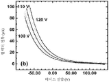
도 12는, 듀퐁 7162 반투명 도체 및 p 타입 실리콘 잉크를 이용하여 인쇄된 접점들을 가진 다른 유사한 트랜지스터에 대한 유사한 데이터를 도시한다. 3개의 장치들에 대한 변환 특성들은 개별적인 부품들로 구성된 모델 트랜지스터의 변환 특성들(도 3)과 유사하고, 베이스 전류가 음일 때 베이스 전류에 대한 컬렉터 전류가 선형 의존성을 가지며, 베이스 전류가 양일 때 작은 오프-전류를 가진다. Figure 12 shows similar data for other similar transistors with printed contacts using DuPont 7162 translucent conductor and p type silicon ink. The conversion characteristics for the three devices are similar to the conversion characteristics (Figure 3) of a model transistor made up of discrete components, and the collector current for the base current has a linear dependence when the base current is negative, Has a small off-current.
더욱 구체적으로, 도 12는, 평면 종이 기판에 반투명 도전성 산화물 접점들 및 p 타입 실리콘 반도체를 스크린 인쇄함으로써 제조된 제 3 실시형태에 따른 트랜지스터의 변환 특성을 도시하고, 120V의 컬렉터 전위에 있어서 베이스 전류에 대한 컬렉터 전류의 의존성(도 12a) 및 100V, 110V 및 120V의 컬렉터 전위에 있어서 베이스 전위에 대한 컬렉터 전류의 의존성(도 12b)을 보여준다. More specifically, Fig. 12 shows the conversion characteristics of the transistor according to the third embodiment produced by screen printing semitransparent conductive oxide contacts and p-type silicon semiconductor on a flat paper substrate, and shows the base current (Fig. 12A) and the dependence of collector current on base potential at collector potentials of 100V, 110V and 120V (Fig. 12B).
도 13은, 제곱미터 당 80 그램의 비코팅 평면 백상지 기판에 은 및 p 타입 실리콘 잉크의 스크린 인쇄에 의해 제조된 도 7a 내지 7c의 제 4 실시형태의 트랜지스터의 사진을 도시한다. 본 실시형태의 다른 실시예들도 또한 이전의 실시예들에서 설명된 물질들을 이용하여 제조되었다. 13 shows a photograph of the transistor of the fourth embodiment of Figs. 7A to 7C produced by screen printing of silver and p type silicon inks on a non-coated flat paper substrate of 80 grams per square meter. Other embodiments of this embodiment have also been fabricated using the materials described in the previous embodiments.
도 14는, 도 7b에 도시된 제 4 실시형태의 트랜지스터에 대한 전류-전류(도 14a) 및 전류-전압(도 14b) 변환 특성들을 도시하고, 이전의 실시형태의 변환 특성들과 대체로 비슷하여, 음의 베이스 전류에 대한 컬렉터 전류의 선형 의존성을 가지지만, 양의 베이스 전류에 대해 약한 선형 의존성을 보여주는 약간 높은 오프-전류를 가진다. 그러나, 대칭 구성은, 비대칭 디자인과 비교하여 전류-전압 변환 특성 곡선들에서 더 높은 경사를 가지는 것처럼(도 14b), 전류가 변환되는 베이스 전위를 더 잘 정의한다. 이러한 스위치 온 전압은 컬렉터에 인가된 전위에 의존한다. 14 shows the current-to-current (FIG. 14A) and current-voltage (FIG. 14B) conversion characteristics for the transistor of the fourth embodiment shown in FIG. 7B and is substantially similar to the conversion characteristics of the previous embodiment Has a linear dependence of the collector current on the negative base current, but has a slightly higher off-current showing a weak linear dependence on the positive base current. However, the symmetry configuration better defines the base potential at which the current is converted, as if it had a higher slope in the current-voltage conversion characteristic curves as compared to the asymmetric design (Fig. 14b). This switch-on voltage depends on the potential applied to the collector.
더욱 구체적으로, 도 14는, 평면 종이 기판에 은 접점들 및 p 타입 실리콘 반도체를 스크린 인쇄함으로써 제조된 제 4 실시형태에 따른 트랜지스터의 변환 특성을 도시하고, 90V, 110V 및 130V의 컬렉터 전위에 있어서 베이스 전류에 대한 컬렉터 전류의 의존성(도 14a) 및 90V, 110V 및 130V의 컬렉터 전위에 있어서 베이스 전위에 대한 컬렉터 전류의 의존성(도 14b)을 보여준다. More specifically, Fig. 14 shows the conversion characteristics of the transistor according to the fourth embodiment produced by screen-printing silver contacts and p-type silicon semiconductor on a planar paper substrate, and shows the conversion characteristics at 90 V, 110 V and 130 V collector potential 14A) and the dependence of the collector current on the base potential at the collector potentials of 90V, 110V and 130V (FIG. 14B).
도 15는 제 4 실시형태의 특징과 제 5 실시형태의 특징을 결합한 본 발명의 제 6 예시적 실시형태를 도시한다.Fig. 15 shows a sixth exemplary embodiment of the present invention combining the features of the fourth embodiment and the features of the fifth embodiment.
도전성 베이스, 이미터 및 컬렉터 단자들(86, 88, 90)은 절연면을 가진 기판(64) 상에 인쇄된다. 각각의 접점은, 서로에 대해 120도 방향을 가진 3개의 축들을 정의하는 안쪽으로 연장된 도전성 트랙(92, 94, 96)을 가진다. 각각의 트랙(92, 94, 96)의 양 측면에는, 동심원 커브 형태로 서로 맞물려 있는 접점들(98, 100, 102)의 세트들이 연장되어 있다. 단자들 및 서로 맞물려 있는 접점들의 패턴은, 이전의 실시형태들에서 설명된 물질 및 공정을 이용하여 기판에 적층된다. The conductive base, emitter and
접점들(98, 100, 102)은 도 15에 도시된 것처럼, 일련의 원호들을 형성할 수도 있고, 또는 3각형 또는 6각형과 같은 3회 대칭을 가진 다각형의 부분들일 수 있다. 그 다음에, 반도체 몸체(104)는 이전에 설명된 것과 동일한 방식으로 접점들 사이의 갭들을 브릿지하도록 적층된다. 선택적으로, 적층의 순서가 뒤바뀌어, 반도체 패턴이 접점들과 기판 사이에 위치할 수도 있다.
유리하게는, 각 쌍의 단자들 사이의 배리스터들의 상대 저항들은, 3회 대칭 및 3개의 단자들로의 용이한 접근을 유지하면서, 도전성 접점들 사이의 반도체 브릿지의 길이, 폭 및 개수를 변경함으로써 자유롭게 변화될 수 있다. Advantageously, the relative resistances of the varistors between each pair of terminals can be varied by varying the length, width, and number of semiconductor bridges between the conductive contacts while maintaining easy symmetry and easy access to the three terminals It can be changed freely.
Claims (22)
각각의 단자들을 형성하는 3개 이상의 도전성 접점들을 형성하는 도전성 물질을 포함하는 전자 장치로서,
상기 반도체 물질 및 상기 도전성 접점들은 상기 전자 장치를 형성하기 위해 적어도 부분적으로 오버랩하며, 어느 한 쌍의 단자들 사이의 상기 전자 장치의 전기적 특성들은 배리스터의 전기적 특성들에 대응하는 것을 특징으로 하는 전자 장치. The body of the semiconductor material, and
An electronic device comprising a conductive material forming at least three conductive contacts forming respective terminals,
Wherein the semiconductor material and the conductive contacts at least partially overlap to form the electronic device wherein the electrical characteristics of the electronic device between the pair of terminals correspond to electrical characteristics of the varistor .
제 1 단자로의 양 전류가 있을 때, 양 전위가 인가되는 제 2 단자를 통한 미세 전류, 및 상기 제 2 단자에 대하여 음 전위로 유지되는 제 3 단자로부터의 양 전류가 있으며; 상기 제 1 단자의 바깥으로의 음 전류가 있을 때, 상기 제 2 단자로의 양 전류, 및 상기 제 3 단자를 통한 미세 전류가 있는 방식으로, 하나의 단자와 나머지 2개의 단자들 사이의 전류의 전환을 가능하게 하는 각 쌍의 단자들 사이의 배리스터 특성들을 갖는 것을 특징으로 하는 전자 장치. 5. The method according to any one of claims 1 to 4,
There is a fine current through a second terminal to which a positive potential is applied and a positive current from a third terminal to be held at a negative potential with respect to the second terminal when there is a positive current to the first terminal; The current between the one terminal and the remaining two terminals is changed in such a manner that there is a negative current to the second terminal and a fine current through the third terminal when there is a negative current to the outside of the first terminal. And varistor characteristics between each pair of terminals enabling conversion.
배리스터 특성들은, 다수의 대칭 반도체 접합들이 입자들 사이의 계면에 형성되는 상기 반도체 물질에서의 상기 대칭 반도체 접합들로부터 생겨나는 것을 특징으로 하는 전자 장치. 6. The method of any one of claims 1 to 5, wherein the semiconductor material is a particulate or particulate material,
Wherein the varistor characteristics arise from the symmetric semiconductor junctions in the semiconductor material in which a plurality of symmetric semiconductor junctions are formed at interfaces between the particles.
배리스터 특성들은, 다수의 무작위로 배향되거나 대향하는 정류 접합들이 상기 2개의 전기적으로 상이한 물질들 사이의 계면에 형성되는 상기 반도체 물질에서의 상기 정류 접합들로부터 생겨나는 것을 특징으로 하는 전자 장치. 6. A method according to any one of claims 1 to 5, wherein the semiconductor material is a composition comprising at least two electrically different materials,
The varistor characteristics arise from the rectifying junctions in the semiconductor material in which a plurality of randomly oriented or opposing rectifying junctions are formed at the interface between the two electrically different materials.
3개 이상의 단자들이 상기 반도체 물질 층의 일면에 동일면을 형성하며 배치되어 있는 것을 특징으로 하는 전자 장치. 2. The semiconductor device of claim 1, further comprising a layer of semiconductor material deposited on the substrate,
And three or more terminals are arranged on one surface of the semiconductor material layer to form the same surface.
상기 1개 이상의 추가 접점은 추가 몸체 또는 접지 접점을 형성하는 것을 특징으로 하는 전자 장치. 12. A device according to any one of the preceding claims, comprising at least one further contact point and a layer of insulating material disposed between at least one of the further contact points and the body of another contact or semiconductor material,
Said at least one further contact forming an additional body or ground contact.
각각의 단자들을 형성하기 위해 상기 반도체 물질의 몸체에 3개 이상의 도전성 접점들을 제공하는 단계를 포함하고,
어느 한 쌍의 단자들 사이의 전자 장치의 전기적 특성들은 배리스터의 전기적 특성들에 대응하는 것을 특징으로 하는 전자 장치를 제조하는 방법. Providing a body of semiconductor material, and
Providing three or more conductive contacts to the body of semiconductor material to form respective terminals,
Wherein electrical characteristics of the electronic device between a pair of terminals correspond to electrical characteristics of the varistor.
기판 상에 적어도 제 1 층의 반도체 물질을 적층하는 단계, 및
각각의 단자들을 형성하기 위해 3개 이상의 도전성 접점들을 형성하는 도전성 물질을 적층하는 단계를 더 포함하고,
상기 반도체 물질 및 상기 도전성 접점들은 상기 전자 장치를 형성하기 위해 적어도 부분적으로 오버랩하는 것을 특징으로 하는 전자 장치를 제조하는 방법. 15. The electronic device manufacturing method according to claim 14,
Laminating at least a first layer of semiconductor material on a substrate, and
Further comprising laminating a conductive material to form three or more conductive contacts to form respective terminals,
Wherein the semiconductor material and the conductive contacts at least partially overlap to form the electronic device.
상기 반도체 물질은 상기 도전성 물질에 의해 형성된 접점들과 적어도 부분적으로 오버랩하게 적층되는 것을 특징으로 하는 전자 장치를 제조하는 방법. 16. The method of claim 15, wherein the conductive material is first deposited on the substrate,
Wherein the semiconductor material is at least partially overlapped with contacts formed by the conductive material. ≪ RTI ID = 0.0 > 11. < / RTI >
상기 접점들을 형성하는 도전성 물질은 상기 반도체 물질 위에 적층되는 것을 특징으로 하는 전자 장치 제조 방법. 16. The method of claim 15, wherein the semiconductor material is deposited first,
Wherein the conductive material forming the contacts is deposited on the semiconductor material.
기판에 반도체 물질 층을 적층하는 단계, 및
상기 반도체 물질 층의 3개 이상의 단자들을 동일면으로 적층하는 단계를 더 포함하는 것을 특징으로 하는 전자 장치를 제조하는 방법. 19. The method according to any one of claims 14 to 18,
Laminating a layer of semiconductor material on a substrate, and
≪ / RTI > further comprising laminating three or more terminals of the layer of semiconductor material in the same plane.
반도체 물질의 몸체를 플레이트, 층 또는 디스크의 형태로 제공하는 단계,
2개 이상의 단자들을 상기 몸체의 일면에 형성하는 단계, 및
1개 이상의 단자를 상기 몸체의 타면에 형성하는 단계를 더 포함하는 것을 특징으로 하는 전자 장치를 제조하는 방법. 15. The method of claim 14,
Providing a body of semiconductor material in the form of a plate, layer or disc,
Forming two or more terminals on one side of the body, and
Further comprising the step of forming at least one terminal on the other side of the body.
절연 물질 층을 다른 접점들 또는 상기 반도체 물질의 몸체 중 적어도 하나 위에 적층하는 단계, 및
1개 이상의 추가 접점을 상기 절연 물질 층에 형성하는 단계를 더 포함하고,
상기 1개 이상의 추가 접점은 추가 몸체 또는 접지 접점을 형성하는 것을 특징으로 하는 전자 장치를 제조하는 방법. 21. The method according to any one of claims 14 to 20,
Depositing a layer of insulating material on at least one of the other contacts or the body of the semiconductor material; and
Further comprising forming one or more additional contacts in the layer of insulating material,
Wherein the at least one additional contact forms an additional body or ground contact.
반도체 물질의 몸체를 한 쌍의 대향하는 면들을 갖는 원통 또는 정각 기둥의 형태로 제공하는 단계,
제 1 단자 및 제 2 단자를 각각 상기 대향하는 면들에 형성하는 단계, 및
1개 이상의 단자를 상기 대향하는 면들을 연결하는 표면에 형성하는 단계를 더 포함하는 것을 특징으로 하는 전자 장치를 제조하는 방법. 15. The method of claim 14,
Providing a body of semiconductor material in the form of a cylinder or square column having a pair of opposing surfaces,
Forming a first terminal and a second terminal on the opposing surfaces, respectively, and
Forming at least one terminal on a surface connecting said opposing surfaces. ≪ RTI ID = 0.0 > 11. < / RTI >
Applications Claiming Priority (3)
| Application Number | Priority Date | Filing Date | Title |
|---|---|---|---|
| ZA2012/07163 | 2012-09-25 | ||
| ZA201207163 | 2012-09-25 | ||
| PCT/IB2013/058692 WO2014049500A1 (en) | 2012-09-25 | 2013-09-20 | Current switching transistor |
Publications (1)
| Publication Number | Publication Date |
|---|---|
| KR20150066547A true KR20150066547A (en) | 2015-06-16 |
Family
ID=50387078
Family Applications (1)
| Application Number | Title | Priority Date | Filing Date |
|---|---|---|---|
| KR1020157010907A KR20150066547A (en) | 2012-09-25 | 2013-09-20 | Current switching transistor |
Country Status (7)
| Country | Link |
|---|---|
| US (1) | US9601604B2 (en) |
| EP (1) | EP2901492A4 (en) |
| JP (1) | JP2016500914A (en) |
| KR (1) | KR20150066547A (en) |
| CN (1) | CN104662670B (en) |
| WO (1) | WO2014049500A1 (en) |
| ZA (1) | ZA201502852B (en) |
Families Citing this family (2)
| Publication number | Priority date | Publication date | Assignee | Title |
|---|---|---|---|---|
| US9431205B1 (en) | 2015-04-13 | 2016-08-30 | International Business Machines Corporation | Fold over emitter and collector field emission transistor |
| USD848384S1 (en) * | 2017-08-17 | 2019-05-14 | Epistar Corporation | Transistor |
Family Cites Families (25)
| Publication number | Priority date | Publication date | Assignee | Title |
|---|---|---|---|---|
| CA272437A (en) | 1925-10-22 | 1927-07-19 | Edgar Lilienfeld Julius | Electric current control mechanism |
| US2524033A (en) | 1948-02-26 | 1950-10-03 | Bell Telephone Labor Inc | Three-electrode circuit element utilizing semiconductive materials |
| US2524035A (en) | 1948-02-26 | 1950-10-03 | Bell Telphone Lab Inc | Three-electrode circuit element utilizing semiconductive materials |
| US2569347A (en) | 1948-06-26 | 1951-09-25 | Bell Telephone Labor Inc | Circuit element utilizing semiconductive material |
| FR2241875B1 (en) * | 1973-08-21 | 1977-09-09 | Radiotechnique Compelec | |
| JPS5816602B2 (en) * | 1979-02-09 | 1983-04-01 | ティーディーケイ株式会社 | Voltage nonlinear resistance element |
| GB2044531B (en) * | 1979-02-09 | 1983-05-25 | Tdk Electronics Co Ltd | Non-linear resistance elements and method for manufacturing same |
| JPS5735303A (en) * | 1980-07-30 | 1982-02-25 | Taiyo Yuden Kk | Voltage vs current characteristic nonlinear semiconductor porcelain composition and method of producing same |
| JPH01146305A (en) * | 1987-12-03 | 1989-06-08 | Nec Corp | Metal oxide varistor |
| JP2712046B2 (en) * | 1989-10-18 | 1998-02-10 | 宇部興産株式会社 | Liquid crystal display |
| JP2556151B2 (en) * | 1989-11-21 | 1996-11-20 | 株式会社村田製作所 | Stacked Varistor |
| JPH05275958A (en) * | 1992-03-25 | 1993-10-22 | Murata Mfg Co Ltd | Noise filter |
| JP2001023805A (en) * | 1999-07-09 | 2001-01-26 | Matsushita Electric Ind Co Ltd | Manufacture of varistor |
| DE10059498A1 (en) | 2000-11-30 | 2002-06-13 | Infineon Technologies Ag | Substrate with a semiconducting layer, electronic component with this substrate, electronic circuit with at least one such electronic component, printable composition and method for producing a substrate |
| EP1593163B1 (en) | 2003-01-30 | 2015-06-17 | PST Sensors (Pty) Limited | A thin film semiconductor device and method of manufacturing a thin film semiconductor device |
| JP2005340301A (en) * | 2004-05-24 | 2005-12-08 | Tdk Corp | Voltage-dependent nonlinear resistor |
| KR20060103864A (en) * | 2005-03-28 | 2006-10-04 | 타이코 일렉트로닉스 코포레이션 | Surface mount multi-layer electrical circuit protection device with active element between pptc layers |
| JP4487963B2 (en) * | 2006-03-27 | 2010-06-23 | Tdk株式会社 | Varistor and light emitting device |
| WO2008010437A1 (en) * | 2006-07-20 | 2008-01-24 | Otowa Electric Co., Ltd. | Lead line extracting type spd and spd manufacturing method |
| US8203421B2 (en) * | 2008-04-14 | 2012-06-19 | Shocking Technologies, Inc. | Substrate device or package using embedded layer of voltage switchable dielectric material in a vertical switching configuration |
| US20100159259A1 (en) * | 2008-12-19 | 2010-06-24 | Lex Kosowsky | Voltage switchable dielectric material incorporating p and n type material |
| CN102550132A (en) * | 2009-03-26 | 2012-07-04 | 肖克科技有限公司 | Components having voltage switchable dielectric materials |
| US20110132645A1 (en) * | 2009-12-04 | 2011-06-09 | Ning Shi | Granular varistor and applications for use thereof |
| JP5543190B2 (en) * | 2009-12-17 | 2014-07-09 | 株式会社日本自動車部品総合研究所 | Rotation detector |
| US9320135B2 (en) * | 2010-02-26 | 2016-04-19 | Littelfuse, Inc. | Electric discharge protection for surface mounted and embedded components |
-
2013
- 2013-09-20 EP EP13840678.0A patent/EP2901492A4/en not_active Withdrawn
- 2013-09-20 WO PCT/IB2013/058692 patent/WO2014049500A1/en active Application Filing
- 2013-09-20 KR KR1020157010907A patent/KR20150066547A/en not_active Application Discontinuation
- 2013-09-20 US US14/430,585 patent/US9601604B2/en not_active Expired - Fee Related
- 2013-09-20 JP JP2015532558A patent/JP2016500914A/en active Pending
- 2013-09-20 CN CN201380049979.5A patent/CN104662670B/en not_active Expired - Fee Related
-
2015
- 2015-04-24 ZA ZA2015/02852A patent/ZA201502852B/en unknown
Also Published As
| Publication number | Publication date |
|---|---|
| WO2014049500A1 (en) | 2014-04-03 |
| US9601604B2 (en) | 2017-03-21 |
| CN104662670A (en) | 2015-05-27 |
| JP2016500914A (en) | 2016-01-14 |
| EP2901492A1 (en) | 2015-08-05 |
| US20150236140A1 (en) | 2015-08-20 |
| CN104662670B (en) | 2019-03-12 |
| EP2901492A4 (en) | 2016-06-22 |
| ZA201502852B (en) | 2016-11-30 |
Similar Documents
| Publication | Publication Date | Title |
|---|---|---|
| Lüssem et al. | Vertical organic transistors | |
| Fujimoto et al. | Fabrication of a vertical-type organic transistor with a planar metal base | |
| US6414543B1 (en) | Rectifying charge storage element | |
| US20080197343A1 (en) | Organic Field Effect Transistor Gate | |
| US7652339B2 (en) | Ambipolar transistor design | |
| JP5382763B2 (en) | SEMICONDUCTOR ELEMENT, ITS MANUFACTURING METHOD, AND ELECTRONIC DEVICE HAVING THE SEMICONDUCTOR ELEMENT | |
| JP2019525461A (en) | Amorphous metal hot electron transistor | |
| JP2005513802A (en) | Organic field effect transistor having offset threshold voltage and use thereof | |
| Kraft et al. | Printed and organic diodes: devices, circuits and applications | |
| KR20150066547A (en) | Current switching transistor | |
| KR101487443B1 (en) | Transistor for reforming dielectric film surface and the product method thereof | |
| US7579620B2 (en) | Field-effect transistor comprising a layer of an organic semiconductor | |
| JP5898226B2 (en) | Diode, its use, and method for manufacturing it | |
| GB2552488A (en) | Field-effect transistor and method for the production thereof | |
| CN105932049A (en) | Nanometer diode device and preparation method thereof | |
| KR101499075B1 (en) | Transistor for reforming dielectric film surface and the product method thereof | |
| CN109791988A (en) | Decker and its manufacturing method | |
| Kawanishi et al. | High-mobility organic single crystal transistors with submicrometer channels | |
| US20090108253A1 (en) | Electronic component | |
| Kaschura | The Organic Permeable Base Transistor: Operation Principle and Optimizations | |
| JP6123413B2 (en) | Thin film transistor array and image display device | |
| US20080237584A1 (en) | Organic Component and Electric Circuit Comprising Said Component | |
| Fujimoto et al. | Large current modulation in novel vertical-type organic transistor using sheet metal base | |
| WO2012037474A1 (en) | Two-and three-terminal molecular electronic devices with ballistic electron transport | |
| Fujimoto et al. | High Performance Vertical Organic Transistor Using Sheet Metal Base |
Legal Events
| Date | Code | Title | Description |
|---|---|---|---|
| E902 | Notification of reason for refusal | ||
| E601 | Decision to refuse application |