KR20150064174A - Imaging optical system and method for manufacturing lens array - Google Patents
Imaging optical system and method for manufacturing lens array Download PDFInfo
- Publication number
- KR20150064174A KR20150064174A KR1020157011453A KR20157011453A KR20150064174A KR 20150064174 A KR20150064174 A KR 20150064174A KR 1020157011453 A KR1020157011453 A KR 1020157011453A KR 20157011453 A KR20157011453 A KR 20157011453A KR 20150064174 A KR20150064174 A KR 20150064174A
- Authority
- KR
- South Korea
- Prior art keywords
- optical system
- lens
- lens optical
- imaging
- light
- Prior art date
Links
Images


Classifications
-
- G—PHYSICS
- G02—OPTICS
- G02B—OPTICAL ELEMENTS, SYSTEMS OR APPARATUS
- G02B3/00—Simple or compound lenses
- G02B3/0006—Arrays
- G02B3/0037—Arrays characterized by the distribution or form of lenses
- G02B3/0062—Stacked lens arrays, i.e. refractive surfaces arranged in at least two planes, without structurally separate optical elements in-between
-
- B—PERFORMING OPERATIONS; TRANSPORTING
- B29—WORKING OF PLASTICS; WORKING OF SUBSTANCES IN A PLASTIC STATE IN GENERAL
- B29C—SHAPING OR JOINING OF PLASTICS; SHAPING OF MATERIAL IN A PLASTIC STATE, NOT OTHERWISE PROVIDED FOR; AFTER-TREATMENT OF THE SHAPED PRODUCTS, e.g. REPAIRING
- B29C33/00—Moulds or cores; Details thereof or accessories therefor
- B29C33/38—Moulds or cores; Details thereof or accessories therefor characterised by the material or the manufacturing process
- B29C33/3842—Manufacturing moulds, e.g. shaping the mould surface by machining
-
- G—PHYSICS
- G02—OPTICS
- G02B—OPTICAL ELEMENTS, SYSTEMS OR APPARATUS
- G02B13/00—Optical objectives specially designed for the purposes specified below
- G02B13/001—Miniaturised objectives for electronic devices, e.g. portable telephones, webcams, PDAs, small digital cameras
- G02B13/0015—Miniaturised objectives for electronic devices, e.g. portable telephones, webcams, PDAs, small digital cameras characterised by the lens design
- G02B13/002—Miniaturised objectives for electronic devices, e.g. portable telephones, webcams, PDAs, small digital cameras characterised by the lens design having at least one aspherical surface
-
- G—PHYSICS
- G02—OPTICS
- G02B—OPTICAL ELEMENTS, SYSTEMS OR APPARATUS
- G02B3/00—Simple or compound lenses
- G02B3/0006—Arrays
-
- G—PHYSICS
- G02—OPTICS
- G02B—OPTICAL ELEMENTS, SYSTEMS OR APPARATUS
- G02B3/00—Simple or compound lenses
- G02B3/0006—Arrays
- G02B3/0012—Arrays characterised by the manufacturing method
- G02B3/0025—Machining, e.g. grinding, polishing, diamond turning, manufacturing of mould parts
-
- G—PHYSICS
- G02—OPTICS
- G02B—OPTICAL ELEMENTS, SYSTEMS OR APPARATUS
- G02B3/00—Simple or compound lenses
- G02B3/0006—Arrays
- G02B3/0012—Arrays characterised by the manufacturing method
- G02B3/0031—Replication or moulding, e.g. hot embossing, UV-casting, injection moulding
-
- G—PHYSICS
- G02—OPTICS
- G02B—OPTICAL ELEMENTS, SYSTEMS OR APPARATUS
- G02B3/00—Simple or compound lenses
- G02B3/0006—Arrays
- G02B3/0037—Arrays characterized by the distribution or form of lenses
- G02B3/0056—Arrays characterized by the distribution or form of lenses arranged along two different directions in a plane, e.g. honeycomb arrangement of lenses
-
- G—PHYSICS
- G03—PHOTOGRAPHY; CINEMATOGRAPHY; ANALOGOUS TECHNIQUES USING WAVES OTHER THAN OPTICAL WAVES; ELECTROGRAPHY; HOLOGRAPHY
- G03G—ELECTROGRAPHY; ELECTROPHOTOGRAPHY; MAGNETOGRAPHY
- G03G15/00—Apparatus for electrographic processes using a charge pattern
- G03G15/04—Apparatus for electrographic processes using a charge pattern for exposing, i.e. imagewise exposure by optically projecting the original image on a photoconductive recording material
-
- H—ELECTRICITY
- H04—ELECTRIC COMMUNICATION TECHNIQUE
- H04N—PICTORIAL COMMUNICATION, e.g. TELEVISION
- H04N1/00—Scanning, transmission or reproduction of documents or the like, e.g. facsimile transmission; Details thereof
- H04N1/024—Details of scanning heads ; Means for illuminating the original
- H04N1/028—Details of scanning heads ; Means for illuminating the original for picture information pick-up
- H04N1/02805—Details of scanning heads ; Means for illuminating the original for picture information pick-up with photodetectors arranged in a two-dimensional array
-
- H—ELECTRICITY
- H04—ELECTRIC COMMUNICATION TECHNIQUE
- H04N—PICTORIAL COMMUNICATION, e.g. TELEVISION
- H04N1/00—Scanning, transmission or reproduction of documents or the like, e.g. facsimile transmission; Details thereof
- H04N1/024—Details of scanning heads ; Means for illuminating the original
- H04N1/028—Details of scanning heads ; Means for illuminating the original for picture information pick-up
- H04N1/03—Details of scanning heads ; Means for illuminating the original for picture information pick-up with photodetectors arranged in a substantially linear array
- H04N1/031—Details of scanning heads ; Means for illuminating the original for picture information pick-up with photodetectors arranged in a substantially linear array the photodetectors having a one-to-one and optically positive correspondence with the scanned picture elements, e.g. linear contact sensors
- H04N1/0311—Details of scanning heads ; Means for illuminating the original for picture information pick-up with photodetectors arranged in a substantially linear array the photodetectors having a one-to-one and optically positive correspondence with the scanned picture elements, e.g. linear contact sensors using an array of elements to project the scanned image elements onto the photodetectors
- H04N1/0312—Details of scanning heads ; Means for illuminating the original for picture information pick-up with photodetectors arranged in a substantially linear array the photodetectors having a one-to-one and optically positive correspondence with the scanned picture elements, e.g. linear contact sensors using an array of elements to project the scanned image elements onto the photodetectors using an array of optical fibres or rod-lenses
-
- H—ELECTRICITY
- H04—ELECTRIC COMMUNICATION TECHNIQUE
- H04N—PICTORIAL COMMUNICATION, e.g. TELEVISION
- H04N1/00—Scanning, transmission or reproduction of documents or the like, e.g. facsimile transmission; Details thereof
- H04N1/024—Details of scanning heads ; Means for illuminating the original
- H04N1/032—Details of scanning heads ; Means for illuminating the original for picture information reproduction
- H04N1/036—Details of scanning heads ; Means for illuminating the original for picture information reproduction for optical reproduction
-
- H—ELECTRICITY
- H04—ELECTRIC COMMUNICATION TECHNIQUE
- H04N—PICTORIAL COMMUNICATION, e.g. TELEVISION
- H04N1/00—Scanning, transmission or reproduction of documents or the like, e.g. facsimile transmission; Details thereof
- H04N1/04—Scanning arrangements, i.e. arrangements for the displacement of active reading or reproducing elements relative to the original or reproducing medium, or vice versa
- H04N1/19—Scanning arrangements, i.e. arrangements for the displacement of active reading or reproducing elements relative to the original or reproducing medium, or vice versa using multi-element arrays
- H04N1/191—Scanning arrangements, i.e. arrangements for the displacement of active reading or reproducing elements relative to the original or reproducing medium, or vice versa using multi-element arrays the array comprising a one-dimensional array, or a combination of one-dimensional arrays, or a substantially one-dimensional array, e.g. an array of staggered elements
- H04N1/192—Simultaneously or substantially simultaneously scanning picture elements on one main scanning line
-
- H—ELECTRICITY
- H04—ELECTRIC COMMUNICATION TECHNIQUE
- H04N—PICTORIAL COMMUNICATION, e.g. TELEVISION
- H04N2201/00—Indexing scheme relating to scanning, transmission or reproduction of documents or the like, and to details thereof
- H04N2201/0077—Types of the still picture apparatus
- H04N2201/0081—Image reader
-
- H—ELECTRICITY
- H04—ELECTRIC COMMUNICATION TECHNIQUE
- H04N—PICTORIAL COMMUNICATION, e.g. TELEVISION
- H04N2201/00—Indexing scheme relating to scanning, transmission or reproduction of documents or the like, and to details thereof
- H04N2201/0077—Types of the still picture apparatus
- H04N2201/0082—Image hardcopy reproducer
-
- H—ELECTRICITY
- H04—ELECTRIC COMMUNICATION TECHNIQUE
- H04N—PICTORIAL COMMUNICATION, e.g. TELEVISION
- H04N2201/00—Indexing scheme relating to scanning, transmission or reproduction of documents or the like, and to details thereof
- H04N2201/024—Indexing scheme relating to scanning, transmission or reproduction of documents or the like, and to details thereof deleted
- H04N2201/02487—Manufacturing details
Abstract
결상 광학계는 제1 방향으로 배열된 복수의 렌즈 광학계를 각각 포함하는 복수의 렌즈 광학계 열을 포함한다. 상기 복수의 렌즈 광학계 열은 상기 제1 방향 및 광축 방향에 수직인 제2 방향으로 배열된다. 상기 복수의 렌즈 광학계 열 각각의 상기 복수의 렌즈 광학계 각각은, 제2 방향에 수직인 단면 내에서는 정립 등배상을 형성하도록 구성되고, 상기 제1 방향에 수직인 단면 내에서는 도립상을 형성하도록 구성된다. 광축 방향에 수직인 단면 내에서, 상기 복수의 렌즈 광학계 열 중 인접하는 렌즈 광학계 열 내의 복수의 렌즈 광학계 각각의 광축은, 제1 방향으로 서로 이격하며, 동일한 선 상에 위치한다.The imaging optical system includes a plurality of lens optical systems each including a plurality of lens optical systems arranged in a first direction. The plurality of lens optical system rows are arranged in the first direction and the second direction perpendicular to the optical axis direction. Wherein each of the plurality of lens optical systems of each of the plurality of lens optical system columns is configured to form a correction image in a cross section perpendicular to the second direction and to form an inverted image in a cross section perpendicular to the first direction do. The optical axes of the plurality of lens optical systems in adjacent lens optical system columns of the plurality of lens optical system columns are spaced from each other in the first direction and located on the same line in a cross section perpendicular to the optical axis direction.
Description
본 발명은 결상 광학계에 관한 것이며, 예를 들어 화상 형성 장치나 화상 판독 장치에 사용되는 결상 광학계에 적합하다.The present invention relates to an imaging optical system, and is suitable, for example, for an imaging optical system used in an image forming apparatus and an image reading apparatus.
최근, 소직경 렌즈 어레이를 포함하는 렌즈 어레이 광학계(결상 광학계)를 사용한 화상 형성 장치 및 화상 판독 장치가 개발되고 있다. 예를 들어, 렌즈 어레이 광학계를 어레이 형상 광원(발광 다이오드(LED))이나 라인 센서와 함께 하우징에 내에 보유 지지한 내장된 유닛을 포함하는 화상 형성 장치 및 화상 판독 장치가 알려져 있다. 이러한 렌즈 어레이 광학계를 사용함으로써 그러한 장치의 크기 및 비용을 감소시킬 수 있다.Recently, an image forming apparatus and an image reading apparatus using a lens array optical system (imaging optical system) including a small diameter lens array have been developed. For example, an image forming apparatus and an image reading apparatus are known, which include an embedded unit in which a lens array optical system is held in a housing together with an array light source (light emitting diode (LED)) or a line sensor. By using such a lens array optical system, the size and cost of such a device can be reduced.
렌즈 어레이 광학계에는, 상 면(image plane)(화상 판독 장치의 경우에는 센서면을 가리키고, 화상 형성 장치의 경우에는 감광면을 가리킨다) 상의 결상 광량 및 결상 성능이 저하되기 쉽고, 결상 광량 및 결상 성능에 불균일이 발생한다는 과제가 있다. 이와 같은 과제를 해결하는 기술이 일본 특허 출원 공개 소63-274915호 및 미국 특허 출원 공개 제2008/0080057호에 제안되고 있다.In the lens array optical system, the imaging light quantity and image forming performance on the image plane (pointing to the sensor surface in the case of an image reading apparatus and pointing to the photosensitive surface in the case of the image forming apparatus) There is a problem in that unevenness occurs in the substrate. A technique for solving such a problem is proposed in Japanese Patent Application Laid-Open No. 63-274915 and U.S. Patent Application Publication 2008/0080057.
일본 특허 출원 공개 소63-274915호에는, 복수의 렌즈 광학계가 일 방향(주배열 방향)으로 배열되는 렌즈 어레이 광학계가 개시되어 있다. 이 렌즈 어레이 광학계는, 주배열 방향 및 광축 방향에 수직인 방향(부배열 방향)에서 보았을 때에, 복수의 렌즈 광학계가 1열로 배열되도록 구성된다. 복수의 렌즈 광학계의 각각에 입사하는 광속은, 부배열 방향에 수직인 단면 내에서는 정립 등배 결상하고, 주배열 방향에 수직인 단면 내에서는 도립 등배 결상한다. 이러한 구성에 의하면, 주배열 방향에 수직인 단면 내에서 정립 등배 결상하는 광학계와 비교하여 부배열 방향에 있어서 필요한 렌즈 파워가 더 작다. 따라서, F 값을 더 작게 해도 양호한 결상 성능이 얻어지고, 이것은 결상 광량과 결상 성능의 양립을 보장할 수 있다.Japanese Patent Application Laid-Open No. 63-274915 discloses a lens array optical system in which a plurality of lens optical systems are arranged in one direction (main array direction). This lens array optical system is configured so that a plurality of lens optical systems are arranged in one row when viewed in a main alignment direction and a direction perpendicular to the optical axis direction (sub-alignment direction). The light beams incident on each of the plurality of lens optical systems form a focal plane in a section perpendicular to the sub-array direction and form a focal plane in a section perpendicular to the main array direction. According to such a configuration, the lens power required in the sub-array direction is smaller than that of the optical system that forms a uniform image within a section perpendicular to the main array direction. Therefore, even if the F value is made smaller, good imaging performance can be obtained, which can ensure the compatibility between the imaging light quantity and the imaging performance.
미국 특허 출원 공개 제2008/0080057호에는, 주배열 방향으로 배열된 렌즈 광학계를 각각 포함하는 2개의 렌즈 광학계 열이 부배열 방향으로 배열된 렌즈 어레이 광학계가 개시되어 있다. 이 렌즈 광학계는 지그재그 형상으로 배열된다. 보다 구체적으로, 렌즈 광학계 열의 각 렌즈 광학계의 광축은 주배열 방향으로 서로 이격된다. 이러한 구성에 의하면, 어레이 형상 광원의 각 발광점으로부터의 광속이 통과하는 렌즈 광학계의 수를 증가되어, 각 발광점 위치에서의 결상 광속이 평균화된다. 그 결과, 결상 광량 및 결상 성능의 불균일을 저감할 수 있다.United States Patent Application Publication No. 2008/0080057 discloses a lens array optical system in which two lens optical system columns each including a lens optical system arranged in the main arrangement direction are arranged in the sub-arrangement direction. The lens optical system is arranged in a zigzag shape. More specifically, the optical axes of the respective lens optical systems of the lens optical system array are spaced apart from each other in the main array direction. According to such a configuration, the number of lens optical systems through which the light fluxes from the respective light emission points of the array light source pass increases, so that the imaging light fluxes at the respective light emission point positions are averaged. As a result, it is possible to reduce unevenness of the imaging light quantity and the imaging performance.
일본 특허 출원 공개 소63-274915호에 개시된 렌즈 어레이 광학계는, 부배열 방향의 렌즈 광학계가 1열을 포함한다. 이러한 구성은, 결상 광량 및 결상 성능의 불균일의 점에서는 불리하다. 미국 특허 출원 공개 제2008/0080057호에 개시된 렌즈 어레이 광학계는, 주배열 방향에 수직인 단면 내에서 물체를 도립 결상하는 계에는 적용할 수 없다. 이러한 구성은, 결상 광량 및 결상 성능의 양립을 보장하는 점에 관해서는 불리하다.In the lens array optical system disclosed in Japanese Patent Application Laid-Open No. 63-274915, the lens optical system in the sub-arrangement direction includes one row. Such a configuration is disadvantageous in terms of unevenness of the imaging light quantity and imaging performance. The lens array optical system disclosed in U.S. Patent Application Publication No. 2008/0080057 can not be applied to a system that forms an object on the basis of a sectional plane perpendicular to the main array direction. Such a configuration is disadvantageous in terms of assuring compatibility between the imaging light amount and imaging performance.
미국 특허 출원 공개 제2008/0080057호에 개시된 것과 마찬가지로, 렌즈 광학계가 부배열 방향(Z 방향)으로 2개의 열이 배치되는 것으로 가정한다. 도 36은, 주배열 방향에 수직인 구성의 단면도(ZX 단면도)를 도시한다. 각 렌즈 광학계는, 일점 쇄선으로 나타낸 광축의 방향(X 방향)으로 나란히 놓인 2개의 렌즈를 포함한다. 이 렌즈는 이상 렌즈(도의 화살표)에 의해 나타내고 있다. 도 36으로부터 알 수 있는 바와 같이, 물체를 정립 등배 결상하는 계에서는, 상측 및 하측의 렌즈 광학계가 동일한 위치에 결상한다. 한편, 물체를 도립 결상하는 계에서는, 렌즈 광학계는 부배열 방향의 별도의 위치에 결상한다. 결상 위치는 서로 일치하지 않는다.As is disclosed in U.S. Patent Application Publication 2008/0080057, it is assumed that the lens optical system has two rows arranged in the sub-arrangement direction (Z direction). Fig. 36 shows a cross-sectional view (ZX cross-sectional view) of a configuration perpendicular to the main array direction. Each lens optical system includes two lenses arranged side by side in the direction of the optical axis (X direction) indicated by the one-dot chain line. This lens is indicated by an abnormal lens (arrows in the figure). As can be seen from Fig. 36, in the system for forming the object by the equal magnification, the upper and lower lens optical systems form an image at the same position. On the other hand, in a system for imaging an object in an on-state, the lens optical system forms an image at a different position in the sub-arrangement direction. The imaging positions do not coincide with each other.
즉, 단순히 일본 특허 출원 공개 소63-274915호 및 미국 특허 출원 공개 제2008/0080057호에 개시된 기술을 조합하더라도, 결상 광량 및 결상 성능이 저하되기 쉽다는 과제와, 결상 광량 및 결상 성능에 불균일이 발생한다는 과제의 양쪽 모두에 대한 해결책을 제공할 수는 없다.That is, even if the technique disclosed in Japanese Patent Application Laid-Open No. 63-274915 and US Patent Application Publication No. 2008/0080057 is simply combined, there is a problem in that the imaging light amount and the imaging performance tend to deteriorate and the problem of unevenness in the imaging light amount and imaging performance It can not provide a solution to both of the problems that arise.
본 발명은 결상 광량과 결상 성능의 양립을 보장할 수 있고, 결상 광량 및 결상 성능의 불균일을 감소시킬 수 있는 결상 광학계에 관한 것이다.The present invention relates to an imaging optical system capable of ensuring compatibility between an imaging light quantity and an imaging performance, and capable of reducing unevenness of an imaging light quantity and an imaging performance.
본 발명의 일 양태에 따르면, 결상 광학계는 제1 방향으로 배열된 복수의 렌즈 광학계를 각각 포함하는 복수의 렌즈 광학계 열을 포함하고, 상기 복수의 렌즈 광학계 열은 상기 제1 방향 및 광축 방향에 수직인 제2 방향으로 배열되고, 상기 복수의 렌즈 광학계 열 각각의 상기 복수의 렌즈 광학계 각각은, 제2 방향에 수직인 단면 내에서는 정립 등배상(erect equal-magnification image)을 형성하도록 구성되고, 상기 제1 방향에 수직인 단면 내에서는 도립상(inverted image)을 형성하도록 구성되며, 광축 방향에 수직인 단면 내에서, 상기 복수의 렌즈 광학계 열 중 인접하는 렌즈 광학계 열의 복수의 렌즈 광학계 각각의 광축은, 제1 방향으로 서로 이격하며, 동일한 선 상에 위치한다.According to an aspect of the present invention, an imaging optical system includes a plurality of lens optical system columns each including a plurality of lens optical systems arranged in a first direction, and the plurality of lens optical system columns are perpendicular to the first direction and the optical axis direction Wherein each of the plurality of lens optical systems of each of the plurality of lens optical systems is configured to form an erect equal-magnification image in a section perpendicular to the second direction, An optical axis of each of a plurality of lens optical systems of adjacent lens optical system columns among the plurality of lens optical system columns is configured so as to form an inverted image in a cross section perpendicular to the first direction, Are spaced apart from each other in the first direction, and are located on the same line.
본 발명의 추가적인 특징은 첨부 도면을 참조해서 아래의 실시예의 설명으로부터 명확해질 것이다.Further features of the present invention will become apparent from the following description of embodiments with reference to the accompanying drawings.
도 1a는 본 실시예에 따른 화상 형성 장치의 개략도.
도 1b는 본 실시예에 따른 컬러 화상 형성 장치의 개략도.
도 2는 본 실시예에 따른 결상 광학계의 개략도.
도 3a, 3b 및 3c는 실시예 1에 따른 결상 광학계의 주요부의 개략도.
도 4a 및 4b는 실시예 1에 따른 렌즈 광학계의 주배열 단면도 및 부배열 단면도.
도 5a, 5b 및 5c는 실시예 1에 따른 각 발광점 위치로부터의 결상 광속을 나타내는 주배열 단면도.
도 6a, 6b 및 6c는 비교예에 따른 각 발광점 위치로부터의 결상 광속을 나타내는 주배열 단면도.
도 7은 실시예 1에 따른 물체 높이와 광 이용 효율비 간의 관계도.
도 8a 및 8b는 실시예 1에 따른 발광점 위치와 광 이용 효율비 간의 관계도.
도 9는 실시예 1에 따른 발광점 위치와 결상 광량비 간의 관계도.
도 10은 비교예에 따른 발광점 위치와 결상 광량비 간의 관계도.
도 11a 및 11b는 실시예 1에 따른 각 발광점 위치로부터의 결상 광속의 결상 성능을 도시하는 도면.
도 12a 및 12b는 비교예에 따른 각 발광점 위치로부터의 결상 광속의 결상 성능을 도시하는 도면.
도 13은 실시예 2에 따른 결상 광학계의 정면 단면도.
도 14a 및 14b는 실시예 2에 따른 발광점 위치와 광 이용 효율비 간의 관계도.
도 15는 실시예 2에 따른 발광점 위치와 결상 광량비 간의 관계도.
도 16a 및 16b는 실시예 2에 따른 각 발광점 위치로부터의 결상 광속의 결상 성능을 도시하는 도면.
도 17은 실시예 3에 따른 결상 광학계의 정면 단면도.
도 18a, 18b 및 18c는 실시예 3에 따른 렌즈 광학계의 주배열 단면도 및 부배열 단면도.
도 19는 실시예 3에 따른 물체 높이와 광 이용 효율비 간의 관계도.
도 20a, 20b 및 20c는 실시예 3에 따른 발광점 위치와 광 이용 효율비 간의 관계도.
도 21은 실시예 3에 따른 발광점 위치와 결상 광량비 간의 관계도.
도 22a 및 22b는 실시예 3에 따른 각 발광점 위치로부터의 결상 광속의 결상 성능을 도시하는 도면.
도 23은 실시예 4에 따른 결상 광학계의 정면 단면도.
도 24a, 24b 및 24c는 실시예 4에 따른 렌즈 광학계의 주배열 단면도 및 부배열 단면도.
도 25는 실시예 4에 따른 물체 높이와 광 이용 효율비 간의 관계도.
도 26a, 26b 및 26c는 실시예 4에 따른 발광점 위치와 광 이용 효율비 간의 관계도.
도 27은 실시예 4에 따른 발광점 위치와 결상 광량비 간의 관계도.
도 28a 및 28b는 실시예 4에 따른 각 발광점 위치로부터의 결상 광속의 결상 성능을 도시하는 도면.
도 29는 본 실시예에 따른 렌즈 어레이의 제조 방법 설명도.
도 30은 본 실시예에 따른 렌즈 어레이의 제조 방법 흐름도.
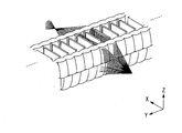
도 31은 본 실시예에 따른 렌즈 어레이의 정면도 및 사시도.
도 32는 본 실시예에 따른 렌즈 어레이의 사시도.
도 33a 및 33b는 본 실시예에 따른 미러 마무리 면 피스(mirror finished surface piece)의 미러 마무리 면의 최종 형상 가공의 설명도.
도 34는 본 실시예에 따른 미러 마무리 면 피스에서의 스코어 라인(score line) 가공의 설명도.
도 35는 본 실시예에 따른 미러 마무리 면 피스 보유 지지 부재의 사시도.
도 36은 지그재그 배열된 종래의 렌즈 어레이의 부배열 단면의 개념도.FIG. 1A is a schematic view of an image forming apparatus according to the present embodiment. FIG.
1B is a schematic view of a color image forming apparatus according to the present embodiment.
2 is a schematic view of an imaging optical system according to the present embodiment.
Figs. 3A, 3B and 3C are schematic views of the main part of an imaging optical system according to
4A and 4B are a main arrangement sectional view and a subordinate arrangement sectional view of the lens optical system according to the first embodiment;
5A, 5B and 5C are main cross-sectional views showing an imaging light flux from each light emitting point position according to the first embodiment;
FIGS. 6A, 6B and 6C are main array cross-sectional views showing an imaging light flux from each light emitting point position according to a comparative example; FIG.
Fig. 7 is a diagram showing the relationship between the object height and the light utilization efficiency ratio according to
8A and 8B are diagrams showing the relationship between the light emitting point position and the light utilization efficiency ratio according to
Fig. 9 is a diagram showing a relationship between a light-emitting point position and an image-forming light amount ratio according to
10 is a diagram showing a relationship between a light emitting point position and an imaging light amount ratio according to a comparative example;
FIGS. 11A and 11B are diagrams showing image forming performance of an imaging light flux from each light emitting point position according to the first embodiment; FIG.
12A and 12B are diagrams showing image forming performance of an imaging light flux from each light emitting point position according to a comparative example;
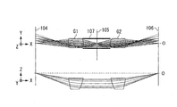
13 is a front cross-sectional view of an imaging optical system according to
14A and 14B are diagrams showing the relationship between light emitting point positions and light utilization efficiency ratios according to
Fig. 15 is a diagram showing the relationship between the light-emitting point position and the imaging light amount ratio according to
16A and 16B are diagrams showing image forming performance of an imaging light flux from each light emitting point position according to the second embodiment;
17 is a front sectional view of the imaging optical system according to the third embodiment.
18A, 18B and 18C are a main arrangement sectional view and a subordinate arrangement sectional view of the lens optical system according to the third embodiment;
19 is a diagram showing a relationship between an object height and a light utilization efficiency ratio according to Embodiment 3. Fig.
20A, 20B and 20C are diagrams showing the relationship between the light emitting point position and the light utilization efficiency ratio according to the third embodiment.
Fig. 21 is a diagram showing the relationship between the light-emitting point position and the imaging light amount ratio according to the third embodiment; Fig.
FIGS. 22A and 22B are diagrams showing image forming performance of an imaging light flux from each light emitting point position according to the third embodiment; FIG.
23 is a front sectional view of the imaging optical system according to the fourth embodiment.
24A, 24B and 24C are a main arrangement sectional view and a subordinate arrangement sectional view of the lens optical system according to the fourth embodiment;
25 is a diagram showing a relationship between an object height and a light utilization efficiency ratio according to
Figs. 26A, 26B and 26C are diagrams showing the relationship between light-emitting-point positions and light utilization efficiency ratios according to
27 is a diagram showing a relationship between a light-emitting point position and an image-forming light amount ratio according to
28A and 28B are diagrams showing image forming performance of an imaging light flux from each light emitting point position according to the fourth embodiment;
29 is an explanatory view of a manufacturing method of a lens array according to the present embodiment.
30 is a flowchart of a manufacturing method of a lens array according to the present embodiment;
31 is a front view and a perspective view of a lens array according to the present embodiment;
32 is a perspective view of the lens array according to the present embodiment;
33A and 33B are explanatory views of the final shape processing of the mirror finished surface of the mirror finished surface piece according to the present embodiment.
34 is an explanatory diagram of a score line processing in a mirror finished surface piece according to the present embodiment;
35 is a perspective view of the mirror finished facepiece holding member according to the present embodiment;
36 is a conceptual diagram of a sub-array section of a conventional lens array arranged in a zigzag arrangement;
본 발명의 각종 실시예, 특징 및 양태에 대해서 도면을 참조해서 아래에서 상세하게 설명한다.Various embodiments, features and aspects of the present invention will be described in detail below with reference to the drawings.
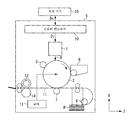
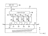
도 1a 및 도 1b는 각각 본 실시예에 따른 화상 형성 장치 및 컬러 화상 형성 장치의 개략도이다(상세한 내용은 후술한다). 본 실시예에서, 화상 형성 장치의 노광 유닛(1) 및 컬러 화상 형성 장치의 노광 유닛(17 내지 20)은 결상 광학계(렌즈 어레이 광학계)를 포함한다. 본 실시예에 따른 결상 광학계를 사용함으로써, 노광 유닛(1 및 17 내지 20)을 콤팩트하게 할 수 있고, 화상 형성 장치 전체의 크기를 작게할 수 있다.Figs. 1A and 1B are schematic views of an image forming apparatus and a color image forming apparatus according to the present embodiment (details will be described later). In this embodiment, the
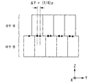
본 실시예에 따른 결상 광학계는, 도 2에 도시한 바와 같이, 제1 방향인 주배열 방향(Y 방향)으로 배열된 복수의 렌즈 광학계를 각각 포함하는 복수의 렌즈 광학계 열을 포함한다. 구체적으로는, 복수의 렌즈 광학계 열이 제2 방향인 부배열 방향(Z 방향)으로 배열된다. 광축 방향(X 방향)에 수직인 단면(YZ 단면) 내에서는, 렌즈 광학계 열에 포함되는 복수의 렌즈 광학계의 광축의 열(광축 열)이 모두 동일한 라인 상에 위치한다. 즉, 각 렌즈 광학계 열의 광축 열의 위치는 부배열 방향으로 동일하게 된다. 보다 구체적으로, 물체면 상의 부배열 방향으로의 위치가 동일한 물체점의 상 면 상의 결상 위치는, 렌즈 광학계 열 사이의 부배열 방향으로 동일하게 된다. (부배열 방향으로 물체면 상의 동일한 위치에 위치하는 물체점은 렌즈 광학계 열에 의해 부배열 방향으로의 동일한 위치에 결상된다.) 이러한 구성은, 주배열 방향에 수직인 단면(ZX 단면) 내에서 물체의 도립 상을 형성하는 어긋난 배열(지그재그 배열)을 제공한다. 이하, 정립 등배 결상하는 계를 정립 등배 결상계라고 한다. 물체를 도립 결상하는 계를 도립 결상계라고 한다.As shown in Fig. 2, the imaging optical system according to this embodiment includes a plurality of lens optical systems each including a plurality of lens optical systems arranged in the main array direction (Y direction) which is the first direction. More specifically, a plurality of lens optical system rows are arranged in the sub-arrangement direction (Z direction) which is the second direction. In the cross section (YZ cross section) perpendicular to the optical axis direction (X direction), the columns (optical axis columns) of the optical axes of the plurality of lens optical systems included in the lens optical system are all located on the same line. That is, the positions of the optical axis arrays of the respective lens optical system columns are the same in the sub-array direction. More specifically, the imaging positions on the image plane of the object point at the same position in the sub-arrangement direction on the object plane are the same in the sub-arrangement direction between the lens optical system columns. (The object point located at the same position on the object plane in the sub-array direction is imaged at the same position in the sub-arrangement direction by the lens optical system row). This configuration is such that, in the cross section perpendicular to the main array direction (Zigzag arrangement) for forming an inverted image of the image. Hereinafter, the system which forms the image by the equalization is referred to as the image equalization system. A system that performs on-imaging of an object is referred to as a in-phase imaging system.
본 실시예에서 사용된 "어긋난 배열(지그재그 배열)"은, 복수의 렌즈 광학계 열의 인접하는 렌즈 광학계 열 내의 복수의 렌즈 광학계 각각의 광축이 주배열 방향으로 서로 이격하는 구성을 말한다. 본 실시예에서는, 렌즈 광학계 열이 부배열 방향으로 인접해서 배열되어 있는 것을, "복수의 렌즈 광학계 열이 부배열 방향으로 배열되고 있다"라고 표현한다. 이러한 표현은, 렌즈 광학계 열이 서로 주배열 방향으로 어긋나 있는 어긋난 배열의 구성을 포함한다. 본 실시예에서 사용된 "부배열 방향으로 인접하는 렌즈 광학계 열"이란, 부배열 방향으로 가장 가까이 놓여있는 것을 말한다. 예를 들어, 렌즈 광학계 열이 그 사이에 중간 부재를 개재해서 배열되고 있어, 렌즈 광학계 열이, 엄밀한 의미에서 서로 밀착하고 있지 않다고 가정한다. 그러한 경우에도, 렌즈 광학계 열은 "인접하는 렌즈 광학계 열"이라고 부른다.Quot; misaligned arrangement (zigzag arrangement) "used in this embodiment refers to a configuration in which optical axes of a plurality of lens optical systems in adjacent lens optical system columns of a plurality of lens optical system columns are spaced from each other in the main array direction. In this embodiment, the fact that the lens optical system columns are arranged adjacently in the sub-arrangement direction is expressed as "a plurality of lens optical system columns are arranged in the sub-arrangement direction ". This expression includes a configuration of a shifted arrangement in which the lens optical system rows are displaced from each other in the main alignment direction. The term " lens optical system column adjacent in the sub-arrangement direction "used in this embodiment means a lens system that lies closest to the sub-arrangement direction. For example, it is assumed that the lens optical system rows are arranged with the intermediate member therebetween, and the lens optical system columns are not in close contact with each other in a strict sense. Even in such a case, the lens optical system row is referred to as "adjacent lens optical system row ".
본 실시예에 따른 결상 광학계는 도립 결상계의 어긋남 배열을 제공할 수 있다. 이것은, 결상 광량과 결상 성능 간의 양립을 확보할 수 있고, 결상 광량 및 결상 성능의 불균일을 저감할 수 있다.The imaging optical system according to this embodiment can provide a misalignment arrangement of the imaging system. This can ensure compatibility between the imaging light amount and the imaging performance, and it is possible to reduce unevenness of the imaging light amount and the imaging performance.
이하, 본 실시예에 따른 결상 광학계에 대해서, 구체적인 실시예와 관련하여 상세하게 설명한다.Hereinafter, the imaging optical system according to the present embodiment will be described in detail with reference to specific embodiments.
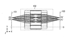
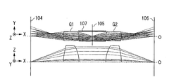
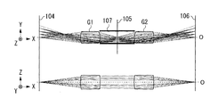
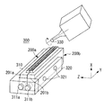
도 3a, 3b 및 3c는 실시예 1에 따른 결상 광학계(102)의 주요부의 개략도이다. 도 3a는 XY 단면, 도 3b는 ZX 단면, 도 3c는 YZ 단면을 나타낸다. 이하, XY 단면(부배열 방향에 수직인 단면)은 주배열 단면이라고 한다. ZX 단면(주배열 방향에 수직인 단면)은 부배열 단면이라고 한다. 본 실시예에서는, 결상 광학계(102)가 화상 형성 장치의 노광 유닛(1) 내에 배치된다는 가정하에 설명한다.3A, 3B and 3C are schematic views of the main part of the imaging
본 실시예에 따른 결상 광학계(102)는 부배열 방향(Z 방향)으로 배열된 2개의 렌즈 광학계 열을 포함한다. 렌즈 광학계 열은 각각 주배열 방향(Y 방향)으로 배열된 복수의 렌즈 광학계를 포함한다. 도 3a에 도시된 바와 같이, 광원(101)의 발광점으로부터 출사된 광속은 렌즈 광학계를 통과하여, 감광 유닛(103) 상의 한 점에 집광된다. 예를 들어, 광원(101)의 발광점 P1로부터의 광속은 점 P1'에 집광된다. 발광점 P2로부터의 광속은 점 P2'에 집광된다. 이 구성에 의해, 광원(101)의 발광 상태에 대응하는 노광이 가능하게 된다. 도 3a 및 3b에서, 렌즈 광학계의 광축 O를 파선으로 나타내고 있다.The imaging
광원(101)은 주배열 방향으로 규칙적인 간격으로 배열된 복수의 발광점을 포함한다. 인접하는 발광점 간의 간격은 수십 μm이다. 인접하는 발광점 간의 간격은 인접하는 렌즈 광학계 간의 간격(수백 μm 이상)에 비하여 충분히 작다. 따라서, 이하에서 발광점은 전반적으로 연속적으로 존재하는 것으로 간주한다. 광원(101)은 주배열 방향으로 규칙적인 간격으로 배열된 복수의 발광점의 열을, 부배열 방향으로 복수 개 배열함으로써 형성되는, 복수의 발광점의 지그재그 형상의 배열을 포함할 수도 있다. 이러한 구성으로 함으로써, 주배열 방향으로 인접하는 발광점 사이에 충분한 간격을 가능하게 한다. 광원(101)의 예는, LED 어레이를 포함할 수 있다.The
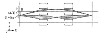
광원(101)의 발광점은 각각, 도 3a에 도시된 주배열 단면(XY 단면) 내에서는 정립 등배 결상하고, 도 3b에 도시된 부배열 단면(ZX 단면) 내에서는 도립 결상한다. 도 3c에 도시된 바와 같이, 부배열 방향으로 배열된 2개의 렌즈 광학계 열의 각각을, 상부 열(top row)(제1 렌즈 광학계 열) 및 하부 열(bottom row)(제2 렌즈 광학계 열)로 부른다. 상부 열을 이루는 렌즈 광학계 각각의 광축을 속이 채워진 원(●)으로 나타낸다. 하부 열을 이루는 렌즈 광학계의 각각의 광축을 속이 채워진 삼각형(▲)으로 나타낸다. 상부 열 및 하부 열 모두의 렌즈 광학계는 주배열 방향으로 0.76mm의 배열 피치 p를 가진다.The light-emitting points of the
도 3c에 도시한 바와 같이, 상부 열의 각 광축과 하부 열의 광축은 동일한 선(광축 열) 상에 위치하고 있다. 광축 열이 Z=0이라고 하면, Z=-1.22mm 내지 0mm의 범위에 하부 열의 렌즈면이 위치한다. 상부 열의 렌즈면은 Z=0mm 내지 1.22mm의 범위에 있다. 상부 열 및 하부 열을 주배열 방향으로 서로 ΔY 만큼 어긋나게 함으로써, 상부 열 및 하부 열의 광축을 주배열 방향으로 서로 이격시켜서 지그재그 형상으로 배치하고 있다. 상부 열의 광축과 하부 열의 광축 간의 최단 거리는 ΔY로 표시한다. 주배열 방향으로, 하부 열에 렌즈 광학계의 광축을 기준으로 하면, ΔY는 해당 광축에 가장 가까운 상부 열의 렌즈 광학계의 광축까지의 최단 거리이다. 본 실시예에서는, 최단 거리 ΔY를 렌즈 광학계의 주배열 방향의 배열 피치 p의 절반으로 한다. ΔY=(1/2)p(=0.38mm)이다.As shown in Fig. 3C, the optical axes of the respective optical axes and the bottom axes of the upper row are located on the same line (optical axis row). Assuming that the optical axis column is Z = 0, the lens surface of the lower row is located in the range of Z = -1.22 mm to 0 mm. The lens surface of the upper row is in the range of Z = 0 mm to 1.22 mm. The upper and lower rows are displaced from each other by DELTA Y in the main array direction so that the optical axes of the upper row and the lower row are arranged in a staggered configuration in the main array direction. The shortest distance between the optical axis of the upper row and the optical axis of the lower row is denoted by? Y. With reference to the optical axis of the lens optical system in the main row direction and the bottom row,? Y is the shortest distance to the optical axis of the lens optical system of the upper row closest to the optical axis. In this embodiment, the shortest distance DELTA Y is set to be half of the arrangement pitch p in the main array direction of the lens optical system. ? Y = (1/2) p (= 0.38 mm).
표 1은 결상 광학계(102)의 배열 설계값을 나타낸다.Table 1 shows the array design values of the imaging

렌즈 광학계는 각각 제1 렌즈 G1 및 제2 렌즈 G2를 포함한다. 제1 및 제2 렌즈 G1, G2의 입사면 R1 및 출사면 R2(G1R1 면, G1R2 면, G2R1 면, G2R2 면)은 아나몰픽(anamorphic) 비구면으로 구성된다. 그 렌즈 광학계의 각 렌즈면과 광축(X축)의 교점을 원점으로 하고, 주배열 방향으로 광축과 직교하는 축을 Y축, 부배열 방향으로 광축과 직교하는 축을 Z축으로 한다. 그 아나몰픽 비구면의 형상은 이하의 비구면식 (1)로 표현된다.The lens optical system includes a first lens G1 and a second lens G2, respectively. The incident surface R1 and the exit surface R2 (G1R1 surface, G1R2 surface, G2R1 surface, and G2R2 surface) of the first and second lenses G1 and G2 are configured as anamorphic aspherical surfaces. The intersection between each lens surface of the lens optical system and the optical axis (X axis) is defined as the origin, the axis orthogonal to the optical axis in the main array direction is defined as the Y axis, and the axis orthogonal to the optical axis is defined as the Z axis. The shape of the anamorphic aspheric surface is represented by the following aspherical surface expression (1).
![]()
![]()
Ci,j(i, j=0, 1, 2,...)는 비구면 계수이다. 렌즈 광학계 열을 구성하는 각 렌즈 광학계의 렌즈면 중 하나 이상이 주배열 방향 및 부배열 방향으로 제로가 아닌 파워(non-zero power)를 갖는 아나몰픽 비구면이다. 이러한 구성은 결상 성능을 향상시킬 수 있다. 렌즈 광학계의 모든 렌즈면이 아나몰픽 비구면으로 구성될 수도 있다.Ci, j (i, j = 0, 1, 2, ...) is an aspherical surface coefficient. At least one of lens surfaces of each lens optical system constituting the lens optical system row is an anamorphic aspherical surface having a non-zero power in the main array direction and the subordinate array direction. Such a configuration can improve image forming performance. All lens surfaces of the lens optical system may be made of an anamorphic aspherical surface.
표 2는 렌즈 광학계의 광학 설계값을 나타낸다.Table 2 shows the optical design values of the lens optical system.


표 2에 도시한 바와 같이, 본 실시예에서는, 각 렌즈 광학계의 주배열 단면 내에서의 중간 결상 배율 β(상세는 후술)를 -0.45로 설정한다. β는, 렌즈 광학계가 주배열 방향으로 정립 등배 광학계로 기능하기만 하면 어떤 값도 취할 수 있다.As shown in Table 2, in this embodiment, the intermediate imaging magnification? (To be described later in detail) in the main array section of each lens optical system is set to -0.45. beta can take any value as long as the lens optical system functions as a magnification-equalizing optical system in the main array direction.
또한, 표 2에 열거된 계수 C2,0(주 열(main row) 단면 내의 근축 굴절력(paraxial refractive power)에 대응하는 계수)으로부터 G1R1 면(G2R2 면) 및 G1R2 면(G2R1 면) 양자 모두가 광축 근처에서 양의 굴절력을 가짐을 알 수 있다. 또한, 계수 C2,0의 절대값의 크기의 비교로부터 알 수 있는 바와 같이, G1R2 면(G2R1 면)의 굴절력은 G1R1 면(G2R2 면)의 굴절력보다 크다. 즉, G1R2 면(G2R1 면)의 광축 근처에서의 곡률 반경의 절대값은 G1R1 면(G2R2 면)의 그것보다 작다. 그러한 구성은, 중간 결상 배율 β가 0 내지 -1의 범위 내의 값(본 실시예에서는 -0.45)을 취할 때에 구면 수차 및 파일된 곡률(filed curvature)이 감소된 바람직한 결상 기능을 가능하게 한다.In addition, both the G1R1 surface (G2R2 surface) and the G1R2 surface (G2R1 surface) from the coefficient C2,0 (the coefficient corresponding to the paraxial refractive power in the main row section) listed in Table 2, It can be seen that there is a positive refracting power in the vicinity. As can be seen from the comparison of the absolute values of the coefficients C2 and 0, the refractive power of the G1R2 surface (G2R1 surface) is larger than the refractive power of the G1R1 surface (G2R2 surface). That is, the absolute value of the radius of curvature near the optical axis of the G1R2 plane (G2R1 plane) is smaller than that of the G1R1 plane (G2R2 plane). Such a configuration enables a desired image forming function in which the spherical aberration and the filed curvature are reduced when the intermediate imaging magnification β takes a value within a range of 0 to -1 (-0.45 in this embodiment).
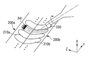
도 4a 및 4b는 각각 본 실시예에 따른 결상 광학계(102)를 구성하는 렌즈 광학계 중 하나의 주배열 단면도(XY 단면도) 및 부배열 단면도(ZX 단면도)를 도시한다.Figs. 4A and 4B respectively show a main arrangement sectional view (XY sectional view) and a subordinate arrangement sectional view (ZX sectional view) of one of the lens optical systems constituting the imaging
도 4a는 상부 열의 렌즈 광학계를 도시한다. 도 4b는 하부 열의 렌즈 광학계를 도시한다.4A shows the lens optical system of the upper row. 4B shows the lens optical system of the bottom row.
도 4a와 4b를 비교하면, 상부 열 및 하부 열을 구성하는 렌즈 광학계는 주배열 단면 내에서는 동일한 구성을 가지며, 부배열 단면 내에서는, 광축 O에 대하여 대칭인 구성을 가짐을 알 수 있다. 상부 열 및 하부 열을 구성하는 렌즈 광학계 각각은, 동일한 광축 O 상에 배치된 제1 광학계(제1 렌즈 G1) 및 제2 광학계(제2 렌즈 G2)를 포함한다. 광원(104)의 각 발광점의 중간 상을 형성하는 광학계를 제1 광학계라고 한다. 제1 광학계가 중간 상을 형성하는 면을 중간 결상면(105)이라고 한다. 중간 결상면(105)에 형성된 중간 상을 상 면(106)에 결상하는 광학계를 제2 광학계라고 한다. 본 실시예에서는, 제1 광학계는 제1 렌즈 G1만을 포함한다. 제2 광학계는 제2 렌즈 G2만을 포함한다.Comparing FIGS. 4A and 4B, it can be seen that the lens optical system constituting the upper and lower rows has the same configuration in the principal arrangement section, and has a configuration symmetrical with respect to the optical axis O in the sub-arrangement section. Each of the lens optical systems constituting the upper row and the lower row includes a first optical system (first lens G1) and a second optical system (second lens G2) arranged on the same optical axis O. An optical system forming an intermediate image of each light emitting point of the
제1 렌즈 G1과 제2 렌즈 G2의 사이에는 차광 부재(107)가 배치된다. 차광 부재(107)는 각각의 렌즈 광학계의 제1 렌즈 G1을 통과하고, 다른 렌즈 광학계의 제2 렌즈 광학계에 입사하는 광속(결상에 기여하지 않는 미광)을 차광하는 역할을 한다.A
도 2에 도시한 바와 같이, 차광 부재(107)의 개구는 렌즈 광학계의 렌즈면의 유효 직경보다 크게 설정되고, 각 발광점으로부터의 광속은 각 렌즈 광학계의 렌즈 면에 의해 제한된다. 즉, 차광 부재(107)는 결상에 기여하는 광속은 차광하지 않고, 결상에 기여하지 않는 미광만을 차단하도록 구성된다. 이러한 구성에 의해, 결상량과 결상 기능 간의 양립이 얻어질 수 있다.2, the opening of the
차광 부재(107)의 개구가 렌즈면의 유효 직경보다 작은 경우에는, 차광 부재(107)는 결상에 기여하는 광속을 바람직하지 않게도 차단할 수 있다. 이러한 문제를 해결하기 위해, 결상량을 확보하기 위해 렌즈면의 유효 직경을 확대하는 방법이 고려될 수 있다. 그러나, 광속을 차단하는 데에 차광 부재(107)가 이용되는 경우에는, 차광 부재(107) 또는 렌즈 광학계 내에서 발생하는 어떠한 위치결정 에러는 광속이 통과하는 렌즈면의 면적을 변화시킬 수 있어서, 바람직한 결상 기능을 얻는 것을 어렵게 한다.When the opening of the
주배열 단면 내에서는, 광원(104)으로부터 출사된 광속은 제1 렌즈 G1을 통과하고, 중간 결상면(105) 상에 중간 상을 형성하고, 제2 렌즈 G2를 통과해서 상 면(106)에 정립 등배 상을 형성한다. 제1 렌즈 G1의 중간 결상면(105) 상의 근축 결상 배율을 중간 결상 배율 β라고 한다. 부배열 단면 내에서는, 광원(104)으로부터 출사된 광속은, 제1 렌즈 G1을 통과하고, 중간 결상을 행하지 않고 제2 렌즈 G2를 통과해서 상 면(106)에 도립 결상한다. 이와 같이, 본 실시예에 따른 결상 광학계(102)는, 부배열 방향으로 도립 결상계로서 구성된다. 이러한 구성은, 결상 성능을 유지한 채로 광의 도입 각도를 크게 할 수 있어, 결상 광량 및 결상 성능의 양립을 달성하고 있다.The light flux emitted from the
상부의 렌즈 광학계 열은 도 4a에 도시된 렌즈 광학계를 복수 개 포함한다. 하부의 렌즈 광학계 열은 도 4b에 도시된 렌즈 광학계를 복수 개 포함한다. 주배열 방향으로 배열된 복서의 제1 렌즈 G1을 제1 렌즈 열이라고 한다. 주배열 방향으로 배열된 복서의 제2 렌즈 G2를 제2 렌즈 열이라고 한다. 이러한 용어에 의해, 결상 광학계(102)는, 부배열 방향으로 배열된 2개의 제1 렌즈를 포함하는 제1 렌즈와, 부배열 방향으로 배열된 2개의 제2 렌즈 열을 포함하는 제2 렌즈 열과, 차광 부재(107)를 결합해서 구성되는 것으로 설명될 수 있다.The upper lens optical system row includes a plurality of lens optical systems shown in Fig. 4A. The lower lens optical system row includes a plurality of lens optical systems shown in Fig. 4B. The first lens G1 of the boxer arranged in the main array direction is referred to as a first lens train. And the second lens G2 of the boxer arranged in the main array direction is referred to as a second lens train. With this terminology, the imaging
본 실시예는, 제1 광학계로서의 제1 렌즈 G1과, 제2 광학계로서의 제2 렌즈 G2를 포함하며, 각 렌즈 광학계는 2개의 렌즈를 포함한다. 그러나, 각 렌즈 광학계는 3개 이상의 렌즈를 포함하여도 된다. 바꿔 말하면, 제1 광학계 및 제2 광학계 중 하나 이상이 2개 이상의 렌즈를 포함할 수도 있다. 3개 이상의 렌즈를 포함하는 렌즈 광학계는 부품 개수를 증가시키기 때문에, 본 실시예와 같이 2 렌즈 구성이 바람직하다. 혹은, 본 실시예에 따른 결상 광학계(102)를 구성하는 렌즈 광학계는 각각 제1 광학계와 제2 광학계와로 분할되지 않고, 1개의 렌즈를 포함할 수도 있다. 그러한 경우에도, 1개의 렌즈가 주배열 단면 내에서는 정립 등배 결상계, 부배열 단면 내에서는 도립 결상계의 역할을 하도록 구성될 수 있다. 그러한 구성은 상술한 바와 같은 2개 이상의 렌즈를 갖는 구성과 마찬가지로 생각할 수 있다.The present embodiment includes a first lens G1 as a first optical system and a second lens G2 as a second optical system, and each lens optical system includes two lenses. However, each lens optical system may include three or more lenses. In other words, at least one of the first optical system and the second optical system may include two or more lenses. Since the lens optical system including three or more lenses increases the number of parts, a two-lens configuration is preferable as in this embodiment. Alternatively, the lens optical system constituting the imaging
본 실시예에서는, 상하부 열을 구성하는 렌즈 광학계는, 렌즈 광학계가 광축(면 정점)을 포함하는 주배열 단면에 의해 절단되고 분할되는 각각의 형상에 대응하는 구성을 가진다. 보다 구체적으로, 주배열 방향으로, 하부 열의 렌즈 광학계의 광축으로부터 해당 광축에 가장 가까운 상부 열의 렌즈 광학계의 광축까지의 최단 거리 ΔY가 0이라고 가정한다(지그재그 형상으로 배열하지 않음). 그러한 경우에, 인접하는 상하부 열을 구성하는 렌즈 광학계의 렌즈면은 동일한 등식에 의해 표현될 수 있는 형상을 가지도록 구성된다. 상하부 열이 중간 부재를 개재해서 배열되어 있는 경우에도, 상하부 열을 구성하는 렌즈 광학계의 렌즈은 동일한 등식에 의해 표현될 수 있는 형상을 가지도록 구성될 수 있으며, 이것은 성형을 용이하게 할 수 있다.In this embodiment, the lens optical system constituting the upper and lower rows has a configuration corresponding to each shape in which the lens optical system is cut and divided by the main array section including the optical axis (surface vertex). More specifically, it is assumed that the shortest distance DELTA Y from the optical axis of the lens system of the lower row to the optical axis of the lens system of the upper row closest to the optical axis in the main array direction is 0 (not arranged in a zigzag shape). In such a case, the lens surface of the lens optical system constituting the adjacent upper and lower rows is configured to have a shape that can be expressed by the same equation. Even when the upper and lower rows are arranged via the intermediate member, the lens of the lens optical system constituting the upper and lower rows can be configured to have a shape that can be expressed by the same equation, which can facilitate the molding.
본 실시예에서는, 상하부 열 각각을 구성하는 렌즈 광학계의 제1 광학계(제1 렌즈 G1)와 제2 광학계(제2 렌즈 G2)가 중간 결상면(105)에 대하여 대칭적으로 구성된다. 이러한 구성으로, 양쪽 광학계에 동일 부재를 사용하는 것이 가능하게 된다. 결상 광학계(102)를 구성하는 모든 렌즈 광학계는 직사각형 형상의 개구를 가지는 렌즈면을 가지는 것이 바람직하다. 보다 구체적으로, 렌즈 광학계의 제1 광학계 및 제2 광학계는 축상 물체 높이를 가지는 광속에 대하여 직사각형의 개구면을 가지도록 구성될 수 있다. 이러한 구성으로, 렌즈면을 가능한 한 밀접하게 배치할 수 있어, 광 이용 효율을 향상시킬 수 있다. 또한, 직사각형 형상이란, 직사각형의 변 중 하나 이상을 곡선으로 한 것과, 정점없이 전반적으로 원 형상 및 전반적으로 타원 형상인 것을 포함하여도 된다.In the present embodiment, the first optical system (first lens G1) and the second optical system (second lens G2) of the lens optical system constituting each of the upper and lower rows are symmetrically configured with respect to the
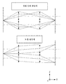
이어서, 각 발광점으로부터 출사되는 광속을 포함하는 결상 광속에 대해서 도 5a 내지 5c를 사용해서 설명한다. 도 5a 내지 5c는 주배열 단면 내에서의, 발광점 위치 A 내지 C로부터 출사되는 결상 광속을 도시하는 도면이다.Next, an imaging light flux including a light flux emitted from each light emitting point will be described with reference to Figs. 5A to 5C. Figs. 5A to 5C are diagrams showing the image forming luminous flux emitted from the luminous point positions A to C in the main array section. Fig.
도 5a 내지 5c에 도시된 바와 같이, 본 실시예에 따른 결상 광학계는, 렌즈 광학계 열의 각 렌즈 광학계의 광축이 인접하는 렌즈 광학계 열 사이의 주배열 방향으로 서로 이격하는 구성을 가진다. 이러한 구성에서, 각 렌즈 광학계는 주배열 단면 내에서 정립 등배 결상계이다. 따라서, 주배열 방향으로의 위치가 물체면 상에서 동일한 발광점의 중간 결상면 상의 결상 위치가 주배열 방향으로 상이하더라도, 결상면 상의 결상 위치는 주배열 방향으로 동일하다.As shown in Figs. 5A to 5C, the imaging optical system according to the present embodiment has a configuration in which the optical axes of the respective lens optical systems of the lens optical system columns are spaced apart from each other in the main array direction between adjacent lens optical system columns. In this configuration, each lens optical system is a stereolithography system in the main alignment section. Therefore, even if the positions in the main array direction on the object plane are different from each other in the main array direction, the imaging positions on the image plane are the same in the main array direction.
도 5a는 렌즈 광학계의 광축 상의 물체 위치인 발광점 위치 A를 도시한다. 발광점 위치 A로부터의 결상 광속은, (광축 상의) 렌즈 광학계의 물체 높이 0의 광속과, 2개의 다른 렌즈 광학계의 물체 높이 (1/2)p의 렌즈 광속을 포함한다. 도 5b는 발광점 위치 A로부터 주배열 방향으로 배열 피치 p의 1/4만큼 이격된 위치인 발광점 위치 B를 도시한다. 발광점 위치 B로부터의 결상 광속은, 2개의 렌즈 광학계의 물체 높이 (1/4)p의 렌즈 광속과, 다른 2개의 렌즈 광학계의 물체 높이 (3/4)p의 렌즈 광속을 포함한다. 도 5c는 발광점 위치 A로부터 배열 피치 p의 1/2만큼 주배열 방향으로 이격된 발광점 위치 C를 도시한다. 발광점 위치 C로부터의 결상 광속은, 2개의 렌즈 광학계의 물체 높이 (1/2)p의 렌즈 광속과, 다른 렌즈 광학계의 광축 상의 렌즈 광속을 포함한다.5A shows a light emitting point position A which is an object position on the optical axis of the lens optical system. The imaging light flux from the light emitting point position A includes the light flux of
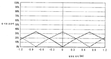
비교예로서, 단지 하나의 렌즈 광학계만을 부배열 방향으로 포함하는 결상 광항계를 고려한다(렌즈 광학계 열의 지그재그 형상의 배열이 없다). 보다 구체적으로, 비교예는 본 실시예에 따른 상하부 렌즈 광학계 열의 광축이 주배열 방향으로 서로 이격하지 않는(최단 거리 ΔY=0) 결상 광학계를 상정한다. 다른 점에서는, 비교예에 따른 결상 광학계는 본 실시예에 따른 결상 광학계(102)와 동일한 구성(광학 설계값)을 가진다.As a comparative example, an imaging optical system including only one lens optical system in the sub-arrangement direction is considered (there is no arrangement of zigzag shapes of lens optical system columns). More specifically, the comparative example assumes an imaging optical system in which the optical axes of the upper and lower lens optical system columns according to the present embodiment are not separated from each other in the main array direction (the shortest distance DELTA Y = 0). In other respects, the imaging optical system according to the comparative example has the same configuration (optical design value) as the imaging
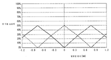
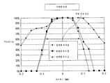
도 6a 내지 6c는 비교예에 따른 결상 광학계에서, 발광점 위치 A 내지 C의 각각으로부터 출사된 광속을 포함하는 결상 광속을 도시한다. 발광점 위치 A로부터의 결상 광속은, 하나의 렌즈 광학계의 물체 높이 0의 렌즈 광속만을 포함한다(도 6a). 발광점 위치 B로부터의 결상 광속은, 하나의 렌즈 광학계의 물체 높이 (1/4)p의 렌즈 광속과, 인접하는 렌즈 광학계의 물체 높이 (3/4)p의 렌즈 광속을 포함한다(도 6b). 발광점 위치 C로부터의 결상 광속은, 인접하는 2개의 렌즈 광학계의 각각의 물체 높이 (1/2)p의 렌즈 광속 2개를 포함한다. 비교예에서는, 각 발광점 위치로부터의 결상 광속은 더 적은 렌즈 광속을 포함한다. 따라서, 발광점 위치 간의 렌즈 광속의 광량의 차이는 결상 광량의 차이에 더 많은 영향을 미친다.6A to 6C show an imaging light flux including a light flux emitted from each of the light emission point positions A to C in the imaging optical system according to the comparative example. The imaging light flux from the light emitting point position A includes only the lens flux of the
도 5a 내지 5c에 도시한 바와 같이, 본 실시예에 따른 결상 광학계(102)에서는, 상하부 렌즈 광학계 열에 어긋난 배열을 적용하면, 결상 광속을 구성하는 렌즈 광속의 수 및 종류(상이한 물체 높이)를 증가시킬 수 있다. 이에 의해, 각 발광점 위치에서의 결상 광속을 평균화하는 것이 가능하게 되어, 결상 광량 및 결상 성능의 불균일을 저감하는 효과를 제공한다. 특히, 본 실시예에서는, 상하부 열의 광축 사이의 이격량 ΔY를, 렌즈 광학계의 주배열 방향의 배열 피치 p의 절반으로 설정한다. 이것은 발광점 위치 A와 C의 결상 광속을 동일하게 할 수 있다.As shown in Figs. 5A to 5C, in the imaging
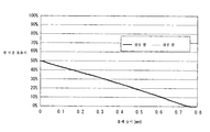
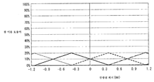
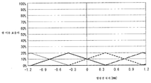
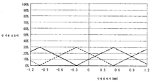
도 7은 본 실시예에 따른 렌즈 광학계의 각 물체 높이에서의 광 이용 효율비를 도시하는 도면이다. 도 7에서는, 상하부 렌즈 광학계 열에서의 각 렌즈 광학계의 광축이 주배열 방향으로 서로 이격하지 않는(최단 거리 ΔY=0) 때에, 광축 상의(물체 높이 0) 광 이용 효율을 100%로 정규화한다. 물체면(광원)으로부터 출사하는 광속의 광량과 상 면(감광 유닛)에 결상하는 광속의 광량의 비를 검사하기 위해서, 개구 효율(광속의 통과 면적에 전반적으로 비례)과 렌즈 광학계의 투과율을 적산함으로써 광 이용 효율이 취득된다. 도 7에 도시한 바와 같이, 본 실시예에 따른 결상 광학계(102)는, 물체 높이가 증가함에 따라 광 이용 효율비가 감소하도록 설계된다. 물체 높이가 배열 피치 p(0.76mm)와 일치할 때에, 광 이용 효율비가 0%가 되도록 설계된다. 도 4a 및 4b에 나타낸 바와 같이, 상부 열의 렌즈 광학계와 하부 열의 렌즈 광학계는, 부배열 단면 내에서 광축 O에 대하여 대칭적으로 구성된다. 따라서, 렌즈 광학계는 각각의 물체 높이에서 동일한 광 이용 효율비를 가진다.Fig. 7 is a diagram showing the light utilization efficiency ratio at each object height of the lens optical system according to the present embodiment. Fig. 7, the light utilization efficiency on the optical axis (object height 0) is normalized to 100% when the optical axes of the respective lens optical systems in the upper and lower lens optical system columns are not spaced apart from each other in the main array direction (shortest distance DELTA Y = 0). In order to examine the ratio of the light amount of the light beam emitted from the object plane (light source) to the light amount of the light beam forming the image plane (photosensitive unit), the aperture efficiency (overall proportion to the passage area of the light flux) Whereby the light utilization efficiency is obtained. As shown in Fig. 7, the imaging
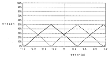
도 8a 및 8b는 렌즈 광학계 열의 각 발광점 위치에서의 광 이용 효율비를 도시한 도면이다. 도 8a는 상부 렌즈 광학계 열에 대응한다. 도 8b는 하부 렌즈 광학계 열에 대응한다. 하부 열에서의 렌즈 광학계의 광축 상의 발광점 위치를 원점으로 상정한다. 광원의 발광점은 주배열 방향으로 전반적으로 연속적으로 존재한다. 도 8a 및 8b로부터 알 수 있는 바와 같이, 광 이용 효율비의 분포는, 배열 피치 p(0.76mm)에서 정점을 가지는 산(mountain) 형이 된다. 이 정점은 각 렌즈 광학계의 광축에 대응한다. 도 8a 및 8b를 비교하면, 상하부 렌즈 광학계 열의 광 이용 효율비의 분포는, 그들의 광축의 최단 거리 ΔY 만큼 어긋나 있음을 알 수 있다.8A and 8B are diagrams showing the light utilization efficiency ratios at the respective light emission point positions of the lens optical system column. 8A corresponds to the upper lens optical system row. 8B corresponds to the lower lens optical system column. The light emitting point position on the optical axis of the lens optical system in the lower row is assumed to be the origin. The light-emitting points of the light source are generally continuous in the main array direction. As can be seen from Figs. 8A and 8B, the distribution of the light utilization efficiency ratios becomes a mountain type having a peak at the arrangement pitch p (0.76 mm). This apex corresponds to the optical axis of each lens optical system. 8A and 8B, it can be seen that the distribution of the light utilization efficiency ratios of the upper and lower lens optical system lines is shifted by the shortest distance DELTA Y of their optical axes.
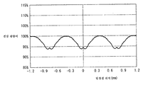
결상 광량의 불균일을 평가하기 위해서, 도 9는 각 발광점 위치에서의 결상 광량비를 나타낸다. 각 발광점 위치의 결상 광량은, 결상 광속을 구성하는 렌즈 광속의 광 이용 효율의 합에 비례한다. 결상 광량은 렌즈 광학계의 광축 상의 발광점 위치의 결상 광량을 100%로서 정규화하고 있다. 도 9로부터, 본 실시예에서는, 결상 광량비의 최댓값과 최솟값의 차가 1.0% 발생하고 있는 것을 안다. 전술한 비교예에 따른 결상 광학계에서의 각 발광점 위치에 대응한 결상 광량의 비를 도 10에 도시한다. 결상 광량비의 최댓값과 최솟값의 차가 6.2% 발생하고 있다. 도 9와 도 10을 비교하면, 본 실시예에 따른 결상 광학계(102)가 결상 광량비의 최댓값과 최솟값의 차가 작고, 결상 광량 불균일이 저감된 것을 안다.To evaluate the unevenness of the imaging light quantity, Fig. 9 shows the imaging light quantity ratio at each light emission point position. The imaging light quantity at each light emission point position is proportional to the sum of the light utilization efficiencies of the lens luminous flux constituting the imaging luminous flux. The imaging light amount is normalized by setting the imaging light amount at the light emission point position on the optical axis of the lens optical system as 100%. It is understood from Fig. 9 that in this embodiment, the difference between the maximum value and the minimum value of the imaging light amount ratio is 1.0%. FIG. 10 shows the ratio of the imaging light quantity corresponding to each light emission point position in the imaging optical system according to the above-described comparative example. The difference between the maximum value and the minimum value of the imaging light amount ratio is 6.2%. Comparing FIG. 9 and FIG. 10, it is known that the imaging
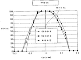
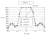
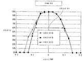
결상 성능 불균일을 평가하기 위해서, 각 발광점 위치의 결상 광속의 결상 성능을 검사한다. 결상 광속의 결상 성능은, 결상 광속을 구성하는 복수의 중첩된 렌즈 광속의 결상 성능을 말한다. 결상 광량(광 이용 효율)과는 상이하게, 결상 성능은 복수의 렌즈 광속의 각각의 결상 성능을 단순하게 더하는 것에 의해서 산출할 수는 없다. 전술한 발광점 위치 A 내지 C의 각각에 대응한 결상 성능을 평가하기 위해서, 콘트라스트와 디포커스의 관계를 도 11a 및 11b에 도시한다. 도 11a는 주배열 단면 내에서의 공통 초점 심도를 나타낸다. 도 11b는 부배열 단면 내에서의 공통 초점 심도를 나타내고 있다. 주배열 방향의 폭이 42.3μm, 부배열 방향의 폭이 25.3μm인 발광점을 발광시켰을 때에, 84.6μm의 주기(600dpi 라인 페어에 상당함)로 반복적으로 더한 결상 광속의 LSF(Line Spread Function)의 분포를 사용해서 콘트라스트를 산출하였다.In order to evaluate the imaging performance irregularity, the imaging performance of the imaging light flux at each light emitting point position is examined. The imaging performance of the imaging light flux means the imaging performance of a plurality of superimposed lens light fluxes constituting the imaging light flux. The imaging performance can not be calculated by simply adding the imaging performance of each of the plurality of lens luminous fluxes differently from the imaging light quantity (light use efficiency). The relationship between contrast and defocus is shown in Figs. 11A and 11B in order to evaluate the imaging performance corresponding to each of the above-mentioned light-emitting point positions A to C. Fig. 11A shows the common depth of focus in the main array section. 11B shows the common depth of focus in the sub-array section. (Line Spread Function) of an imaging light flux repeatedly added at a period of 84.6 占 퐉 (corresponding to a 600 dpi line pair) when a light emitting point having a main alignment direction width of 42.3 占 퐉 and a sub- The contrast was calculated.
마찬가지로, 전술한 비교예에 따른 결상 광학계의 콘트라스트 및 디포커스의 관계를 도 12a 및 12b에 나타낸다. 고정밀의 출력 화상에 대한 요구의 관점에서, 콘트라스트 값 60% 이상에서의 초점 심도를 설명한다. 도 11a 및 11b와, 도 12a 및 12b를 비교하면, 부배열 단면 내에서는, 각 발광점 위치 A 내지 C로부터의 결상 광속의 초점 심도의 변화는 거의 없는 것을 알 수 있다. 주배열 단면 내에서는, 비교예(도 12a)에 따른 초점 심도의 변화는 발광점 위치에 따라 크게 변한다. 본 실시예(도 11a)에 따른 초점 심도의 변화는 발광점 위치에 따라 상당히 적다. 즉, 본 실시예에 따른 결상 광학계(102)에 의하면, 발광점 위치마다의 초점 심도의 변화를 작게 할 수 있고, 이에 의해 결상 성능? 불균일의 저감을 실현할 수 있다.Similarly, the relationship between the contrast and defocus of the imaging optical system according to the comparative example described above is shown in Figs. 12A and 12B. The depth of focus at a contrast value of 60% or more will be described from the viewpoint of a demand for a high-precision output image. Comparing Figs. 11A and 11B with Figs. 12A and 12B, it can be seen that there is almost no change in the depth of focus of the imaging light flux from each light emission point position A to C in the sub-arrangement section. In the main array section, the variation of the depth of focus according to the comparative example (Fig. 12A) largely changes depending on the position of the light emitting point. The variation of the depth of focus according to this embodiment (Fig. 11A) is considerably small depending on the position of the light emitting point. That is, with the imaging
결상 광학계의 결상 성능은, 각 발광점 위치에 대응하는 초점 심도의 공통 범위인 공통 초점 심도에 의해 평가한다. 주배열 단면 내에서, 비교예의 공통 초점 심도는 0.160mm이다. 본 실시예의 공통 초점 심도는 0.180mm이다. 따라서, 본 실시예에서는, 비교예보다 양호한 결상 성능을 실현하고 있다.The imaging performance of the imaging optical system is evaluated by the common depth of focus, which is a common range of the depth of focus corresponding to each light emitting point position. Within the main array section, the common focus depth of the comparative example is 0.160 mm. The common depth of focus of this embodiment is 0.180 mm. Therefore, in the present embodiment, better image forming performance is achieved than in the comparative example.
이와 같이, 본 실시예에 따른 결상 광학계(102)에서는, 결상 광속을 구성하는 렌즈 광속의 수와 종류를 증가시키고, 이에 의해 각 발광점 위치에서의 결상 광속을 평균화한다. 이에 의해, 결상 광량 및 결상 성능의 불균일을 저감하는 효과를 얻고 있다.As described above, in the imaging
각 발광점의 부배열 방향의 물체 높이는, 발광점의 사이즈(25.3μm)의 절반, 즉 12.7μm만큼 작다. 따라서, 본 실시예의 구성에 어긋난 배열을 적용하면, 결상 광량의 변화를 거의 0으로 할 수 있다. 도 11b의 부배열 단면 내에서의 콘트라스트 피크로부터 알 수 있는 바와 같이, 결상 성능의 변화도 거의 없다. 즉, 어긋난 배열을 사용하는 경우에도, 부배열 단면 내에서 결상 광량 및 결상 성능의 양립을 유지할 수 있다.The height of the object in the sub-array direction of each light emitting point is as small as half the size (25.3 mu m) of the light emitting point, i.e., 12.7 mu m. Therefore, by applying an arrangement that is different from the configuration of the present embodiment, the change of the imaging light amount can be made almost zero. As can be seen from the contrast peak in the sub-array section of Fig. 11B, there is almost no change in the imaging performance. That is, even when a misaligned array is used, it is possible to maintain both the amount of image-forming light and the image-forming performance in the sub-array section.
이상과 같이, 본 실시예에 따른 결상 광학계(102)는 부배열 단면 내에 도립 결상계를 형성하고, 어긋난 배열을 사용한다. 이에 의해, 결상 광량과 결상 성능의 양립을 보장하고, 결상 광량 및 결상 성능의 불균일을 저감할 수 있다.As described above, the imaging
렌즈 광학계 열의 각 발광점 위치에서의 결상 광량 및 결상 성능은, 배열 피치 p에서 주기적으로 변동한다. 도 9, 11a 및 11b로부터 알 수 있는 바와 같이, 이러한 변동은 렌즈 광학계의 광축 상의 발광점 위치(발광점 위치 A에 대응함)와, 이 발광점 위치로부터 배열 피치 p의 1/2 어긋난 위치(발광점 위치 C에 대응함)에서 각각 전반적인 피크(peak) 및 전반적인 보텀(bottom)이 발생하도록 된다. 본 실시예에서는, 상하부 열이 동일한 배열 피치 p를 가진다. 광축 열 사이의 최단 거리 ΔY는 배열 피치 p의 1/2이다. 이러한 구성에 의해, 상부 열의 전반적인 피크(및 전반적인 보텀) 및 하부 열의 전반적인 보텀(및 전반적인 피크)를 상쇄할 수 있다. 이 효과는, 도 5a 내지 5c에 도시한 바와 같이, 발광점 위치 A 및 발광점 위치 C에서의 결상 광속이 서로 동일해지는 사실로부터도 알 수 있다. 즉, 본 실시예에 따른 결상 광학계(102)의 구성에 의하면, 결상 광속의 평균화 효과를 보다 크게할 수 있어, 결상 광량 및 결상 성능의 불균일을 보다 저감할 수 있는 효과를 얻을 수 있다.The imaging light quantity and the imaging performance at each light emission point position of the lens optical system line periodically fluctuate at the arrangement pitch p. As can be seen from Figs. 9, 11A and 11B, this fluctuation is caused by the light emitting point position (corresponding to the light emitting point position A) on the optical axis of the lens optical system and the position shifted from the light emitting point position by 1/2 of the array pitch p (Corresponding to the point C), the overall peak and the overall bottom are generated. In the present embodiment, the upper and lower rows have the same arrangement pitch p. The shortest distance DELTA Y between the optical axis rows is 1/2 of the array pitch p. With this arrangement, the overall peak (and overall bottom) of the upper row and the overall bottom (and overall peak) of the lower row can be canceled. This effect can be seen from the fact that the imaging light fluxes at the light emission point position A and the light emission point position C become equal to each other as shown in Figs. 5A to 5C. That is, according to the configuration of the imaging
렌즈 광학계 열의 부배열 방향의 수를 k로 가정한다. 결상 광량 및 결상 성능의 변동을 평균화하는 방법(렌즈 광학계 열의 배치 패턴)은, k≥n≥2를 만족하는 양의 정수 n의 개수, 즉 (k-1) 패턴만큼 존재한다. k열의 렌즈 광학계 열을 조합함으로써, 결상 광량 및 결상 성능의 변동을 평균화할 경우, (n-1) 개의 방식으로 렌즈 광학계 열이 조합될 수 있다. 렌즈 광학계 열의 변동의 전반적인 피크(및 전반적인 보텀)와 전반적인 보텀(및 전반적인 피크)을 더함으로써 평균화를 실행한다. 이때, 결상 광학계(102)의 임의의 2개의 렌즈 광학계 열이, 광축 간의 최단 거리 ΔY가 p/n이 되도록 조합될 경우, 보다 큰 평균 효과가 얻어진다.Let k be the number of sub-arrangement directions of the lens optical system row. The method of averaging the variations of the imaging light quantity and the imaging performance (the arrangement pattern of the lens optical system) exists by the number of the positive integers n satisfying k? N? 2, that is, (k-1) patterns. When the variation of the imaging light quantity and imaging performance is averaged by combining the k lens optical system columns, the lens optical system columns can be combined in (n-1) ways. Averaging is performed by adding the overall peak (and overall bottom) and the overall bottom (and overall peak) of the variation of the lens optic column. At this time, when any two lens optical system columns of the imaging
n이 k≥n≥2를 만족하는 양의 정수라고 가정한다. 전술한 바로부터, (p/n)-1/2×(p/n)=p/(2n)≤ΔY≤(p/n)+1/2×(p/n)=3p/(2n)이다. 결과적으로, 본 발명의 실시예는 렌즈 광학계 열이 아래의 식에 의해 주어지는 조건의 범위 내에 놓이는 경우에 충분한 효과를 제공한다.It is assumed that n is a positive integer satisfying k? n? 2. (P / n) = 1/2 (p / n) = p / (2n) to be. As a result, the embodiment of the present invention provides a sufficient effect when the lens optical system row lies within the range of the condition given by the following equation.
p/(2n)≤ΔY≤3p/(2n) (2)p / (2n)?? Y? 3p / (2n) (2)
이러한 범위를 일탈했을 경우, 전반적인 피크끼리 및 전반적인 보텀이 서로 강화되어 평균화의 효과를 얻지 못해진다.When deviating from this range, the overall peaks and the overall bottom are strengthened with each other and the averaging effect is not obtained.
본 실시예에서는, 렌즈 광학계 열의 수 k=2이다. k≥n≥2를 만족하는 유일한 양의 정수 n은 2이다. 따라서, 렌즈 광학계 열의 배치 패턴은 1개(k-1=2-1=1)가 된다. 렌즈 광학계 열의 조합의 수도 1개이기 때문에, (n-1)=1에 의해 n=2가 된다. 상하부 열의 배열 피치 p=0.76mm이고, 광축 열의 최단 거리 ΔY=(1/2)p이다. 최단 거리 ΔY가 (1/2)p이면, n=2에 대하여 식 (2)를 충족하는 것, 즉 p/4≤ΔY≤3p/4임을 알 수 있다.In this embodiment, the number of lens optical system columns is k = 2. The only positive integer n satisfying k? n? 2 is 2. Therefore, the arrangement pattern of the lens optical system columns is one (k-1 = 2-1 = 1). (N-1) = 1, n = 2 because the number of combinations of the lens optical system columns is one. The arrangement pitch of the upper and lower rows is p = 0.76 mm, and the shortest distance of the row of optical axes is Y = (1/2) p. If the shortest distance DELTA Y is (1/2) p, it can be seen that the equation (2) is satisfied for n = 2, that is, p / 4 DELTA Y 3p / 4.
본 실시예에서는, 렌즈 광속의 수 및 종류를 증가시킴으로써, 각 발광점 위치에서의 결상 광속을 평균화하는 것에 대해서 설명했다. 결상 광속을 구성하는 렌즈 광속의 수는, 렌즈 광학계의 광학 설계값에도 의존하는 것을 알고 있다. 구체적으로는, 물체 높이 0의(광축 상의) 발광점으로부터의 결상 광속을 구성하는 렌즈 광속의 수는, 이하와 같이 구해진다.In this embodiment, the description has been given of averaging the imaging light fluxes at the respective light emission point positions by increasing the number and types of lens light fluxes. It is known that the number of lens luminous fluxes forming the image-forming luminous flux also depends on the optical design value of the lens optical system. Specifically, the number of lens luminous fluxes constituting the image-forming luminous flux from the luminous point of the object height 0 (on the optical axis) is obtained as follows.
주배열 단면 내에서, 렌즈 광학계가 도입할 수 있는 최대의 물체 높이(최외측 축외 물체 높이)는, 렌즈 광학계의 중간 결상면 상에서의 유효 직경이 R이고, 중간 결상 배율이 β인 경우, (-R/2)÷β=R/(2β)에 의해 근사적으로 나타낼 수 있다. 즉, 유효 직경 R의 반값(R/2)은, 최외측 축외 물체 높이의 중간 상의 주배열 방향으로의 결상 위치에 상당한다. 유효 직경 R은, 렌즈 광학계를 구성하는 제1 광학계의 유효 직경을 R1, 제2 광학계의 유효 직경을 R2로 했을 때, R=(R1+R2)/2에 의해 결정된다. 본 실시예와 같이, 제1 광학계(제1 렌즈 G1)의 유효 직경과 제2 광학계(제2 렌즈 G2)의 유효 직경이 동일한 경우에는, 중간 결상면 상에서의 유효 직경 R은 제1 광학계 및 제2 광학계의 유효 직경과 일치한다.The maximum object height (outermost off-axis object height) that can be introduced by the lens optical system in the main alignment section is (-) when the effective diameter on the intermediate imaging plane of the lens optical system is R and the intermediate imaging magnification is? R / 2) /? = R / (2?). That is, the half value (R / 2) of the effective diameter R corresponds to the image forming position in the main array direction in the middle of the outermost off-axis object height. The effective diameter R is determined by R = (R1 + R2) / 2 when the effective diameter of the first optical system constituting the lens optical system is R1 and the effective diameter of the second optical system is R2. When the effective diameter of the first optical system (first lens G1) is equal to the effective diameter of the second optical system (second lens G2) as in the present embodiment, the effective diameter R on the intermediate image- 2 coincides with the effective diameter of the optical system.
렌즈 광학계 열에서의 어떤 렌즈 광학계의 광축 상의 발광점 위치(물체 높이)는, 정수 n과 배열 피치 p에 의해, n×p로서 나타낼 수 있다. 물체 높이의 양과 음을 고려하여, 광축 상의 발광점으로부터의 결상 광속에 포함되는 렌즈 광속의 수는, n×p<│R/(2β)│를 만족하는 정수 n에 의해 부여된다.The light emitting point position (object height) on the optical axis of a certain lens optical system in the lens optical system column can be expressed as n x p by the integer n and the array pitch p. The number of lens fluxes included in the imaging light flux from the light emitting point on the optical axis is given by an integer n satisfying nxp <R / (2?) |
렌즈 광속의 수를 증가시킴으로써, 결상 광량 및 결상 성능의 불균일을 저감할 수 있다. 그러나, 렌즈 광속의 수를 증가시킬 경우, 그로 인한 광학 설계값은 도입하는 광속의 보다 예리한 화각을 포함한다. 그 결과, 구면 수차 및 필드의 곡률을 제거하기 어려워진다. 이러한 단점의 관점에서, 각 렌즈 광학계 열에서, 렌즈 광학계의 광축 상의 발광점 위치로부터의 결상 광속을 구성하는 렌즈 광속의 수가 3개 이하로 되도록 적절한 광학 설계값을 결정한다. 보다 구체적으로, 렌즈 광속의 수가 3개 이하로 되는 광학 설계값의 범위는, 이하의 식 (3)에 의해 나타낼 수 있다.By increasing the number of lens luminous fluxes, it is possible to reduce unevenness of the imaging light quantity and the imaging performance. However, when increasing the number of lens luminous fluxes, the resulting optical design value includes a sharper angle of view of the luminous flux to be introduced. As a result, it becomes difficult to eliminate the spherical aberration and the curvature of the field. In view of such drawbacks, in each lens optical system series, an appropriate optical design value is determined so that the number of lens luminous fluxes constituting the imaging luminous flux from the luminous point position on the optical axis of the lens optical system becomes three or less. More specifically, the range of the optical design value at which the number of the lens luminous fluxes becomes 3 or less can be expressed by the following formula (3).
│R/(2βp)│≤2 (3)R / (2? P)? 2 (3)
이 식 (3)을 만족하도록 광학 설계값을 결정함으로써, 결상 광학계(102)는 수차를 양호하게 보정하면서, 결상 광량 및 결상 성능의 불균일을 저감할 수 있는 효과를 제공할 수 있다. 본 실시예에서는, 상하부 열을 구성하는 렌즈 광학계는 모두 중간 결상 배율 β=-0.45, 중간 결상면 상에서의 유효 직경 R=0.70mm, 배열 피치 p=0.76mm이다. 따라서, │R/(2βp)│=1.02<2가 되어, 상기의 식 (3)을 만족하고 있다.By determining the optical design value so as to satisfy the expression (3), the imaging
이하, 본 발명의 실시예 2에 대해서 설명한다. 실시예 1과 동일 또는 유사한 구성 부분에 대해서는 동일한 참조 부호를 부여한다. 그 설명은 간략화하거나, 혹은 생략한다.A second embodiment of the present invention will be described below. The same or similar constituent parts as those of the first embodiment are denoted by the same reference numerals. The description is simplified or omitted.
도 13은 본 실시예에 따른 결상 광학계의 정면도(YZ 단면도)이다. 본 실시예는, 실시예 1과 마찬가지로, 상하부 열의 광축 열이 동일한 선 상에 위치하도록 구성된다. 본 실시예의 구성은, 상하부 열의 광축 사이의 주배열 방향으로의 최단 거리 ΔY가 (1/4)p(= 0.19mm)라는 점에서 실시예 1과 상이하다. 본 실시예에 따른 렌즈 광학계의 배열의 설계값을 표 3에 나타낸다.13 is a front view (YZ cross-sectional view) of the imaging optical system according to the present embodiment. In this embodiment, similarly to the first embodiment, the optical axis lines of the upper and lower rows are arranged on the same line. The configuration of the present embodiment is different from the first embodiment in that the shortest distance DELAYY in the main array direction between the optical axes of the upper and lower rows is (1/4) p (= 0.19 mm). Table 3 shows the design values of the arrangement of the lens optical system according to this embodiment.

실시예 1과 마찬가지로, 본 실시예에 따른 각 발광점 위치 A 내지 C로부터 출사하는 광속을 포함하는 결상 광속에 대해서 설명한다.As in the first embodiment, an image forming light flux including light fluxes emitted from the respective light emission point positions A to C according to the present embodiment will be described.
발광점 위치 A(하부 열의 렌즈 광학계의 광축 상의 물체면 위치)로부터의 결상 광속은, 렌즈 광학계의 물체 높이 0(광축 상)의 1개의 렌즈 광속과, 렌즈 광학계의 물체 높이 (1/4)p의 1개의 렌즈 광속과, 렌즈 광학계의 물체 높이 (3/4)p의 1개의 렌즈 광속을 포함한다. 발광점 위치 B로부터의 결상 광속은, 렌즈 광학계의 물체 높이 (1/4)p의 1개의 렌즈 광속과, 렌즈 광학계의 물체 높이 (1/2)p의 렌즈 광속 2개를 포함한다. 발광점 위치 C로부터의 결상 광속은, 렌즈 광학계의 물체 높이 (1/2)p의 렌즈 광속 2개와, 렌즈 광학계의 물체 높이 (1/4)p의 렌즈 광속 1개를 포함한다.The image forming light flux from the light emitting point position A (the position of the object plane on the optical axis of the lens system of the lower row) is expressed by one lens flux of the object height 0 (on the optical axis) of the lens optical system, , And one lens flux of the object height (3/4) p of the lens optical system. The imaging light flux from the light emitting point position B includes one lens flux of object height (1/4) p of the lens optical system and two lens fluxes of object height (1/2) p of the lens optical system. The image forming light flux from the light emitting point position C includes two lens fluxes of an object height (1/2) p of the lens optical system and one lens flux of object height (1/4) p of the lens optical system.
이와 같이, 실시예 1과 마찬가지로, 결상 광속을 구성하는 렌즈 광속의 수 및 종류를 증가시킴으로써, 각 발광점 위치에서의 결상 광속을 평균화할 수 있다.Thus, similarly to the first embodiment, by increasing the number and types of lens luminous fluxes constituting the imaging luminous flux, the imaging luminous fluxes at the respective luminous point positions can be averaged.
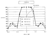
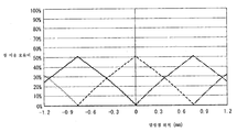
본 실시예에서, 상하부 열의 렌즈 광학계의 각각의 구성은 실시예 1과 마찬가지이다. 따라서, 물체 높이마다의 광 이용 효율비는, 도 7에 나타낸 것과 동일해진다. 발광점 위치마다의 광 이용 효율비는, 도 14a(상부 열) 및 도 14b(하부 열)에 도시한다. 도 14a 및 도 14b를 비교하면, 렌즈 광학계 열의 광축 간의 최단 거리 ΔY만큼 광 이용 효율비의 분포가 어긋나 있는 것을 안다. 도 15는 본 실시예에 따른 발광점 위치마다의 결상 광량의 비를 도시한다. 본 실시예에서는, 결상 광량비의 최댓값과 최솟값의 차가 4.8%인데, 이것은 도 10에 도시한 비교예(6.2%)와 비교해서 더 작다. 이것은 결상 광량의 불균일이 더 작다는 것을 나타낸다.In this embodiment, the respective constitutions of the lens optical systems in the upper and lower rows are the same as those in the first embodiment. Therefore, the light utilization efficiency ratio for each object height is the same as that shown in Fig. The light utilization efficiency ratio for each light emitting point position is shown in Fig. 14A (upper row) and Fig. 14B (lower row). 14A and 14B, it is found that the distribution of light utilization efficiency ratios deviates by the shortest distance DELTA Y between the optical axes of the lens optical system columns. Fig. 15 shows the ratio of the amount of imaging light for each light emitting point position according to this embodiment. In this embodiment, the difference between the maximum value and the minimum value of the imaging light amount ratio is 4.8%, which is smaller than the comparative example (6.2%) shown in Fig. This indicates that the unevenness of the imaging light amount is smaller.
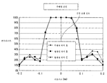
본 실시예에 따른 발광점 위치 A 내지 C로부터의 결상 광속의 결상 성능을 도 16a 및 16b에 나타낸다. 비교예(도 12a 및 12b 참조)와 비교하면, 주배열 단면 내에서는, 콘트라스트 값 60% 이상에 대한 발광점 위치 A 내지 C에 대한 초점 심도의 변화가 작아져, 결상 성능의 불균일이 저감하고 있는 것을 알 수 있다. 콘트라스트 값 60% 이상에서, 주배열 단면 내에서의 공통 초점 심도는 0.167mm이며, 비교예에서의 공통 초점 심도(0.160mm)보다도 큰 것을 안다.16A and 16B show the imaging performance of the imaging light flux from the light emitting point positions A to C according to the present embodiment. Compared with the comparative example (see Figs. 12A and 12B), the variation of the depth of focus with respect to the light emission point positions A to C with respect to the contrast value of 60% or more is reduced within the main array cross section, . At a contrast value of 60% or more, the common depth of focus in the main array section is 0.167 mm, which is larger than the common depth of focus (0.160 mm) in the comparative example.
이와 같이, 본 실시예에 따른 결상 광학계에서는, 결상 광속을 구성하는 렌즈 광속의 수와 종류를 증가시켜, 발광점 위치마다의 결상 광속을 평균화할 수 있다. 이에 의해, 결상 광량 및 결상 성능의 불균일을 저감하는 효과를 얻고 있다.As described above, in the imaging optical system according to the present embodiment, the number and types of the lens luminous flux forming the imaging luminous flux can be increased, and the imaging luminous flux for each luminous point position can be averaged. Thereby, the effect of reducing the unevenness of the imaging light quantity and the imaging performance is obtained.
이상, 본 실시예에 따른 결상 광학계에 의하면, 부배열 단면 내에서 도립 결상계를 형성하고, 어긋난 배열을 사용한다. 이에 의해, 결상 광량과 결상 성능의 양립을 확보할 수 있고, 결상 광량 및 결상 성능의 불균일을 저감할 수 있다.As described above, according to the imaging optical system according to the present embodiment, the inlaid imaging system is formed within the sub-array section and a misaligned array is used. As a result, it is possible to ensure both the image-forming light amount and the image-forming performance, and the unevenness of the image-forming light quantity and the image-forming performance can be reduced.
본 실시예에서는, 최소 간격 ΔY가 (1/2)p로 엄밀하게 설정되는 실시예 1과는 달리, 최소 간격 ΔY=(1/4)p로 설정함으로써, 결상 광속의 평균화를 달성하고 있다. 마찬가지로, 최소 간격이 (1/4)p≤ΔY≤(3/4)p의 범위 내이면, 본 발명의 실시예는 충분한 효과를 얻을 수 있다.In this embodiment, unlike
본 실시예에서도, 렌즈 광학계 열의 수 k는 2이다(즉, n=2). 상하부 열의 배열 피치 p=0.76mm이다. 광축 열의 최단 거리 ΔY=(1/4)p이다. 따라서, 최소 간격 ΔY는 n=2에 대하여 식 (2), 즉 p/4≤ΔY≤3p/4를 충족하는 것을 안다.In this embodiment, the number k of lens optical system columns is 2 (i.e., n = 2). The arrangement pitch of the upper and lower rows is p = 0.76 mm. The shortest distance of the optical axis row is DELTA Y = (1/4) p. Therefore, we find that the minimum spacing DELTA Y satisfies equation (2), i.e. p / 4 DELTA Y &le; 3p / 4, for n =
이하, 본 발명의 실시예 3에 대해서 설명한다. 실시예 1과 동일 또는 유사한 구성 부분에 대해서는 동일한 참조 부호를 부여한다. 그 설명을 간략화하거나, 혹은 생략한다.Hereinafter, a third embodiment of the present invention will be described. The same or similar constituent parts as those of the first embodiment are denoted by the same reference numerals. The description thereof is simplified or omitted.
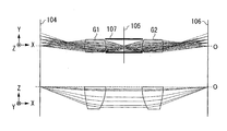
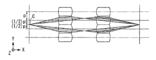
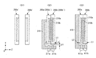
도 17은 본 실시예에 따른 결상 광학계의 개략도이다. 본 실시예는, 실시예 1과는 상이하게, 렌즈 광학계 열을 부배열 방향(Z 방향)으로 3열 배치한 구성이다. 렌즈 광학계 열은, 부배열 방향으로의 음의 방향(-Z 방향)으로 순서대로 하부 열(제3 렌즈 광학계 열), 중간 열(제2 렌즈 광학계 열), 상부 열(제1 렌즈 광학계 열)로 정의한다. 도 17에서는, 상부 열의 렌즈 광학계의 광축을 속이 빈 원(○)으로 나타내고, 중간 열의 렌즈 광학계의 광축을 속이 빈 삼각형(△)으로 나타내고, 하부 열의 렌즈 광학계의 광축을 속이 빈 정사각형(□)으로 나타내고 있다. 도 17로부터 알 수 있는 바와 같이, 본 실시예에 따른 결상 광학계에서는, 상부, 중간 및 하부 열의 모든 렌즈 광학계의 광축이 동일한 선 상에 위치하고 있다. 상하부 열의 렌즈 광학계의 광축이 동일 위치에 존재하고 있다. 상하부 열의 렌즈 광학계는 광축 열에 대하여 부배열 방향으로 대칭적으로 배열된다.17 is a schematic view of an imaging optical system according to this embodiment. This embodiment differs from
도 17에서, 광축 열이 Z=0에 위치하는 것으로 가정한다. Z=-1.22mm 내지 -0.61mm의 범위에 하부 열의 렌즈면이 있다. Z=-0.61mm 내지 0.61mm의 범위에 중간 열의 렌즈면이 있다. Z=0.61mm 내지 1.22mm의 범위에 상부 열의 렌즈면이 있다. 본 실시예에 따른 결상 광학계와 실시예 1에 따른 결상 광학계(102)는, 어긋난 배열을 가지지 않으면, 렌즈 광학계의 면 형상 등의 광학 설계값이 동일해 진다. 상부, 중간, 하부 렌즈 광학계 열은 모두 주배열 방향으로의 배열 피치 p=0.76mm를 가진다.In Fig. 17, it is assumed that the optical axis column is located at Z = 0. Z = -1.22 mm to -0.61 mm in the lower row. There is a middle row of lens surfaces in the range of Z = -0.61 mm to 0.61 mm. There is a lens surface in the upper row in the range of Z = 0.61 mm to 1.22 mm. The imaging optical system according to the present embodiment and the imaging
상하부 열의 렌즈 광학계의 광축이 동일 위치에 존재하기 때문에, 주배열 방향으로, 하부 열의 렌즈 광학계의 광축으로부터 해당 광축에 가장 가까운 상부 열의 렌즈 광학계의 광축까지의 거리 ΔY는 0mm이다. 중간 열의 렌즈 광학계의 광축으로부터 해당 광축에 가장 가까운 상부 열(하부 열)의 렌즈 광학계의 광축까지의 최단 거리 ΔY는 (1/2)p(=0.38mm)이다. 이 배열 설계값을 표 4에 나타낸다.The distance DELTA Y from the optical axis of the lens system of the lower row to the optical axis of the lens system of the upper row closest to the optical axis in the main array direction is 0 mm because the optical axes of the lens systems of the upper and lower rows exist at the same position. The shortest distance? Y from the optical axis of the lens system of the middle row to the optical axis of the lens system of the upper row (lower row) closest to the optical axis is (1/2) p (= 0.38 mm). Table 4 shows the array design values.

상부, 중간, 하부 열의 각각을 구성하는 렌즈 광학계의 주배열 단면도(XY 단면도) 및 부배열 단면도(ZX 단면도)를 도 18a, 18b, 18c에 나타낸다. 도 18a, 18b, 18c로부터 알 수 있는 바와 같이, 상부, 중간, 하부 열을 구성하는 렌즈 광학계는 주배열 단면 내에서는 같은 구성을 가지지만, 부배열 단면 내에서는 다른 구성을 가진다. 상하부 열의 렌즈 광학계는, 부배열 단면 내에서 보았을 때에는, 광축 O에 대하여 부배열 방향으로 대칭적으로 구성된다.Figs. 18A, 18B and 18C show a main arrangement sectional view (XY sectional view) and a subordinate sectional view (sectional view ZX) of the lens optical system constituting each of the upper, middle and lower rows. As can be seen from Figs. 18A, 18B and 18C, the lens optical system constituting the upper, middle, and lower rows has the same configuration in the principal arrangement section, but has different configurations in the sub-arrangement section. The lens optical systems in the upper and lower rows are symmetrically arranged in the sub-arrangement direction with respect to the optical axis O when viewed in the sub-arrangement section.
실시예 1과 마찬가지로, 본 실시예에 따른 각 발광점 위치 A 내지 C로부터 출사하는 광속을 포함하는 결상 광속에 대해서 설명한다.As in the first embodiment, an image forming light flux including light fluxes emitted from the respective light emission point positions A to C according to the present embodiment will be described.
발광점 위치 A(중간 열의 렌즈 광학계의 광축 상의 물체면 위치)로부터의 결상 광속은, 중간 열의 렌즈 광학계의 물체 높이 0(광축 상)의 렌즈 광속 1개와, 상부 열의 렌즈 광학계의 물체 높이 (1/2)p의 렌즈 광속 2개와, 하부 열의 렌즈 광학계의 물체 높이 (1/2)p의 렌즈 광속 2개를 포함한다. 발광점 위치 B로부터의 결상 광속은, 중간 열의 렌즈 광학계의 각 물체 높이 (1/4)p 및 물체 높이 (3/4)p의 렌즈 광속 2개와, 상부 열의 렌즈 광학계의 각 물체 높이 (1/4)p 및 물체 높이 (3/4)p의 렌즈 광속 2개와, 하부 열의 렌즈 광학계의 각 물체 높이 (1/4)p 및 물체 높이 (3/4)p의 렌즈 광속 2개로 구성된다. 발광점 위치 C로부터의 결상 광속은, 중간 열의 렌즈 광학계의 물체 높이 (1/2)p의 렌즈 광속 2개와, 상부 열의 렌즈 광학계의 광축 상의 렌즈 광속 1개와, 하부 열의 렌즈 광학계의 광축 상의 렌즈 광속 1개를 포함한다.The image forming luminous flux from the light emitting point position A (the position of the object plane on the optical axis of the lens system of the middle row) is one of the lens luminous flux of the object height 0 (on the optical axis) of the lens system of the middle row, 2) p and two lens beams of an object height (1/2) p of the lens system of the lower row. The image forming luminous flux from the luminous point position B is obtained by two lens luminous fluxes having the object height (1/4) p and the object height (3/4) p of the middle-row lens optical system, 4) p and the object height (3/4) p, and the object lens height (1/4) p and object height (3/4) p of the lens system in the lower row. The image forming light flux from the light emitting point position C is formed by two lens fluxes of an object height (1/2) p of the middle-row lens optical system and one lens flux on the optical axis of the lens system of the upper row, 1 < / RTI >
즉, 실시예 1과 마찬가지로, 결상 광속을 구성하는 렌즈 광속의 수 및 종류를 증가시킴으로써, 각 발광점 위치에서의 결상 광속을 평균화할 수 있다. 본 실시예에서는, 렌즈 광속의 종류는, 물체 높이의 차이뿐만 아니라, 렌즈 광속을 사출하는 상이한 렌즈 광학계 열 또한 가리킨다.That is, similarly to the first embodiment, by increasing the number and types of lens luminous fluxes constituting the imaging luminous flux, the imaging luminous fluxes at the respective luminous point positions can be averaged. In this embodiment, the type of the lens luminous flux refers not only to the difference in object height, but also to different lens optical system radiating the lens luminous flux.
도 19는 본 실시예에 따른 상부, 중간, 하부 열의 렌즈 광학계의 물체 높이마다의 광 이용 효율비를 나타낸 것이다. 본 실시예에서의 광 이용 효율비는 실시예 1(도 7 참조)에 대하여 스케일링된다. 상하부 열의 렌즈 광학계의 구성은 부배열 방향으로 대칭이기 때문에, 물체 높이마다의 광 이용 효율비는 동일해진다. 상하부 열과 중간 열의 렌즈 광학계는 부배열 단면 내에서 보았을 때에 다른 구성이기 때문에, 물체 높이마다의 광 이용 효율비가 크게 상이한 것을 안다. 도 20a, 20b, 20c는 발광점 위치마다의 상부, 중간, 하부 열의 광 이용 효율비를 도시한다. 광 이용 효율비의 분포는, 각각의 렌즈 광학계 열의 광축 간의 최단 거리 ΔY만큼 어긋나 있는 것을 안다.19 shows the light utilization efficiency ratios for the object heights of the upper, middle, and lower rows of the lens optical system according to the present embodiment. The light utilization efficiency ratio in this embodiment is scaled with respect to Embodiment 1 (see Fig. 7). Since the configuration of the lens optical system in the upper and lower rows is symmetrical in the sub-arrangement direction, the light utilization efficiency ratio is the same for each object height. Since the lens optical systems of the upper and lower rows and the middle row have different structures when viewed in the sub-array section, it is known that the light utilization efficiency ratio for each object height is greatly different. 20A, 20B, and 20C show the light utilization efficiency ratios of the upper, middle, and lower rows for each light emitting point position. The distribution of the light utilization efficiency ratios is found to be shifted by the shortest distance DELTA Y between the optical axes of the respective lens optical system columns.
본 실시예에 따른 발광점 위치마다의 결상 광량비를 도 21에 나타낸다. 본 실시예에서는, 결상 광량비의 최댓값과 최솟값의 차가 2.9%이며, 이것은 도 10에 도시한 비교예(6.2%)와 비교해서 더 작다. 이에 의해, 결상 광량 불균일이 저감하고 있는 것을 안다.FIG. 21 shows the imaging light amount ratio for each light emitting point position according to this embodiment. In this embodiment, the difference between the maximum value and the minimum value of the imaging light amount ratio is 2.9%, which is smaller than the comparative example (6.2%) shown in Fig. As a result, it is known that the unevenness of the imaging light quantity is reduced.
본 실시예에 따른 발광점 위치 A 내지 C의 각각으로부터의 결상 광속의 결상 성능을 도 22a 및 22b에 나타낸다. 비교예(도 12a, 12b 참조)와 비교하여, 발광점 위치 A 내지 C에 대한 초점 심도의 변화가 작아져, 결상 성능 불균일이 저감하고 있는 것을 안다. 콘트라스트 값 60% 이상에서, 주배열 단면 내에서의 공통 초점 심도는 0.173mm이며, 비교예에서의 공통 초점 심도(0.160mm)보다 큰 것을 안다.22A and 22B show the imaging performance of the imaging light flux from each of the light emitting point positions A to C according to the present embodiment. It is understood that the variation of the depth of focus with respect to the positions A to C of the light emitting points is smaller than that in the comparative example (see Figs. 12A and 12B), and the image forming performance unevenness is reduced. At a contrast value of 60% or more, the common depth of focus in the main array section is 0.173 mm, which is larger than the common depth of focus (0.160 mm) in the comparative example.
본 실시예에 따른 결상 광학계에서는, 결상 광속을 구성하는 렌즈 광속의 수와 종류를 증가시켜서, 발광점 위치마다의 결상 광속을 평균화할 수 있다. 이에 의해, 결상 광량 및 결상 성능의 불균일을 저감하는 효과를 얻고 있다.In the imaging optical system according to the present embodiment, it is possible to increase the number and kinds of lens luminous fluxes constituting the imaging luminous flux, and to average out the imaging luminous fluxes at each luminous point position. Thereby, the effect of reducing the unevenness of the imaging light quantity and the imaging performance is obtained.
이상, 본 실시예에 따른 결상 광학계는 부배열 단면 내에서 도립 결상계를 형성하고, 어긋난 배열을 사용한다. 이에 의해, 결상 광량과 결상 성능의 양립을 확보하고, 결상 광량 및 결상 성능의 불균일을 저감할 수 있다.As described above, the imaging optical system according to the present embodiment forms an inlaid imaging system in a sub-array section and uses a misaligned arrangement. Thus, it is possible to secure both the image-forming light amount and the image-forming performance, and to reduce unevenness of the image-forming light quantity and image forming performance.
본 실시예에서는, 렌즈 광학계 열의 수는 k=3이다. 상부, 중간, 하부 열의 배열 피치 p=0.76mm이다. 상부 및 중간 열의 광축 열 간의 최단 거리는 ΔY=(1/2)p이다. 중간 및 하부 열의 광축 열 간의 최단 거리 ΔY=(1/2)p이다. 본 실시예에 따른 결상 광학계에서는, 렌즈 광학계 열이 광축 열에 대하여 부배열 방향으로 대칭적으로 배열되고 있다. 보다 구체적으로, 결상 광학계는 유사한 렌즈 광학계 열의 조합을 2개 포함한다(상부 및 중간 열과, 중간 및 하부 열). 즉, (n-1)=1에 의해 n=2이다. 상부 열과 중간 열의 조합 및 중간 열과 하부 열의 조합의 모두에서, 식 (2), 즉 p/4≤ΔY≤3p/4를 충족하는 것을 안다. 즉, 실시예 1과 마찬가지로, 발광점 위치마다의 중간 열의 결상 광량 및 결상 성능의 변동의 전반적인 피크(및 전반적인 보텀)와, 상하부 열의 결상 광량 및 결상 성능의 변동의 전반적인 보텀(및 전반적인 피크)을 상쇄할 수 있어 보다 큰 평균화 효과를 얻고 있다.In this embodiment, the number of lens optical system columns is k = 3. The arrangement pitch of the upper, middle, and lower rows is p = 0.76 mm. The shortest distance between the upper and middle rows of optical axes is? Y = (1/2) p. The shortest distance between the optical axis columns of the middle and bottom rows is? Y = (1/2) p. In the imaging optical system according to the present embodiment, the lens optical system columns are symmetrically arranged in the sub-array direction with respect to the optical axis. More specifically, the imaging optical system includes two combinations of similar lens optical system columns (upper and middle rows, middle and lower rows). That is, n = 2 by (n-1) = 1. (2), i.e., p / 4 &le; Y &le; 3p / 4, in both the combination of the upper row and the middle row and the combination of the middle row and the lower row. That is, similarly to the first embodiment, the overall peak (and the overall bottom) of the amount of the imaging light in the intermediate row and the fluctuation of the imaging performance for each light emitting point position and the overall bottom (and the overall peak) Can be canceled, and a larger averaging effect is obtained.
이하, 본 발명의 실시예 4에 대해서 설명한다. 실시예 1과 동일 또는 유사한 구성 부분에 대해서는 동일한 참조 부호를 부여한다. 그 설명을 간략화 혹은 생략한다.A fourth embodiment of the present invention will be described below. The same or similar constituent parts as those of the first embodiment are denoted by the same reference numerals. The description thereof is simplified or omitted.
도 23은 본 실시예에 따른 결상 광학계의 개략도이다. 본 실시예는, 실시예 3과 마찬가지로, 부배열 방향으로 배치된 3개의 렌즈 광학계 열을 포함한다. 본 실시예는, 상부, 중간, 하부 열의 렌즈 광학계의 Z 방향의 범위 및 광축 간의 최단 거리 ΔY에 있어서 실시예 3과 상이하다. 도 23에서는, 상부 열의 렌즈 광학계의 광축을 속이 채워진 원(●)으로 나타내고, 중간 열의 렌즈 광학계의 광축을 속이 채워진 삼각형(▲)으로 나타내고, 하부 열의 렌즈 광학계의 광축을 속이 채워진 정사각형(■)으로 나타낸다. 도 23으로부터 알 수 있는 바와 같이, 본 실시예에 따른 결상 광학계는, 상부, 중간, 하부 열의 모든 렌즈 광학계의 광축 열이 동일한 선 상에 위치하도록 구성된다.23 is a schematic view of an imaging optical system according to the present embodiment. This embodiment includes three lens optical systems arranged in the sub-arrangement direction as in the third embodiment. The present embodiment is different from the third embodiment in terms of the shortest distance DELTA Y between the optical axis and the range of the lens system of the upper, middle, and lower rows in the Z direction. 23, the optical axis of the lens optical system in the upper row is represented by a filled circle (), the optical axis of the lens system in the middle row is represented by a filled triangle (), and the optical axis of the lens optical system in the lower row is filled with a square . As can be seen from FIG. 23, the imaging optical system according to this embodiment is configured so that the optical axis lines of all the lens optical systems of the upper, middle, and lower rows are located on the same line.
도 23에서, 광축 열의 위치를 Z= 0으로 가정한다. Z=-1.22mm 내지 -0.41mm의 범위에 하부 열의 렌즈면이 있다. Z=-0.41mm 내지 0.41mm의 범위에 중간 열의 렌즈면이 있다. Z=0.41mm 내지 1.22mm의 범위에 상부 열의 렌즈면이 있다. 본 실시예에 따른 결상 광학계와 실시예 1에 따른 결상 광학계(102)는, 어긋난 배열을 가지지 않을 경우, 렌즈 광학계의 면 형상 등의 광학 설계값이 동일해 진다. 상부, 중간, 하부 렌즈 광학계 열의 주배열 방향의 배열 피치는 모두 p=0.76mm이다.In Fig. 23, it is assumed that the position of the optical axis column is Z = 0. Z = -1.22 mm to -0.41 mm in the lower row. There is a middle row of lens surfaces in the range of Z = -0.41 mm to 0.41 mm. There is a lens surface of the upper row in the range of Z = 0.41 mm to 1.22 mm. When the imaging optical system according to this embodiment and the imaging
주배열 방향으로, 중간 열의 렌즈 광학계의 광축을 기준으로 했을 때, 해당 광축에 가장 가까운 상부 열(하부 열)의 렌즈 광학계의 광축까지의 거리 ΔY는 (1/3)p(=0.253mm)이다. 마찬가지로, 하부 열의 렌즈 광학계의 광축을 기준으로 했을 때, 해당 광축에 가장 가까운 상부 열의 렌즈 광학계의 광축까지의 최단 거리 ΔY는 (1/3)p(= 0.253mm)이다. 이 배열 설계값을 표 5에 나타낸다.The distance? Y to the optical axis of the lens optical system of the upper row (lower row) closest to the optical axis in the main array direction with respect to the optical axis of the lens optical system in the middle row is (1/3) p (= 0.253 mm) . Similarly, when the optical axis of the lens system of the lower row is taken as a reference, the shortest distance DELTA Y to the optical axis of the lens system of the upper row closest to the optical axis is (1/3) p (= 0.253 mm). Table 5 shows the array design values.

상부, 중간, 하부 열의 각각을 구성하는 렌즈 광학계의 주배열 단면도(XY 단면도) 및 부배열 단면도(ZX 단면도)를 도 24a, 24b, 24c에 나타낸다. 도 24a, 24b, 24c로부터 알 수 있는 바와 같이, 상부, 중간, 하부 열을 구성하는 렌즈 광학계는, 주배열 단면 내에서는 같은 구성으로 되어 있지만, 부배열 단면 내에서는 다른 구성으로 된다. 상하부 열을 구성하는 렌즈 광학계는, 부배열 단면 내에서는 광축 O에 대하여 부배열 방향으로 대칭적으로배치된다.Figs. 24A, 24B and 24C show a main arrangement sectional view (XY sectional view) and a subordinate sectional view (sectional view ZX) of the lens optical system constituting each of the upper, middle and lower rows. As can be seen from Figs. 24A, 24B and 24C, the lens optical system constituting the upper, middle, and lower rows has the same configuration in the principal arrangement section, but has a different configuration within the sub-arrangement section. The lens optical systems constituting the upper and lower rows are symmetrically arranged in the sub-arrangement direction with respect to the optical axis O in the sub-arrangement section.
실시예 1과 마찬가지로, 본 실시예에 따른 각각의 발광점 위치 A 내지 C로부터 출사하는 광속을 포함하는 결상 광속에 대해서 설명한다.The image forming beam including the light flux emitted from each of the light emission point positions A to C according to the present embodiment will be described.
발광점 위치 A(중간 열의 렌즈 광학계의 광축 상의 물체면 위치)로부터의 결상 광속은, 중간 열의 렌즈 광학계의 물체 높이 0(광축 상)의 렌즈 광속 1개와, 상부 열의 렌즈 광학계의 물체 높이 (1/3)p 및 (2/3)p 각각의 렌즈 광속 2개와, 하부 열의 렌즈 광학계의 물체 높이 (1/3)p 및 (2/3)p 각각의 렌즈 광속 2개를 포함한다. 발광점 위치 B로부터의 결상 광속은, 중간 열의 렌즈 광학계의 물체 높이 (1/4)p 및 (3/4)p 각각의 렌즈 광속 2개와, 상부 열의 렌즈 광학계의 물체 높이 (1/12)p 및 (11/12)p 각각의 렌즈 광속 2개와, 하부 열의 렌즈 광학계의 물체 높이 (5/12)p 및 (7/12)p 각각의 렌즈 광속 2개를 포함한다. 발광점 위치 C로부터의 결상 광속은, 중간 열의 렌즈 광학계의 물체 높이 (1/2)p의 렌즈 광속 2개와, 상부 열의 렌즈 광학계의 물체 높이 (1/6)p 및 (5/6)p 각각의 렌즈 광속 2개와, 하부 열의 렌즈 광학계의 물체 높이 (5/12)p 및 (1/6)p 각각의 렌즈 광속 2개를 포함한다.The image forming luminous flux from the light emitting point position A (the position of the object plane on the optical axis of the lens system of the middle row) is one of the lens luminous flux of the object height 0 (on the optical axis) of the lens system of the middle row, 3) p and (2/3) p, respectively, and two lens beams of object height (1/3) p and (2/3) p of the lens system of the lower row, respectively. The image forming luminous flux from the luminous point position B is obtained by two lens luminous fluxes each of object height (1/4) p and (3/4) p of the lens system of the middle row and object luminous flux And (11/12) p, and two lens beams of
즉, 실시예 1과 마찬가지로, 결상 광속을 구성하는 렌즈 광속의 수 및 종류를 증가시킴으로써, 발광점 위치마다의 결상 광속을 평균화할 수 있다.That is, similarly to the first embodiment, by increasing the number and kinds of the lens luminous fluxes constituting the imaging luminous flux, the imaging luminous fluxes for each luminous point position can be averaged.
도 25는 본 실시예에 따른 상부, 중간, 하부 열의 렌즈 광학계에서의 물체 높이마다의 광 이용 효율비를 나타낸 것이다. 본 실시예에 따른 광 이용 효율비 또한 실시예 1(도 7 참조)에 따라 스케일링된다. 상하부 열의 렌즈 광학계는 부배열 방향으로 대칭적으로 구성되어, 물체 높이마다의 광 이용 효율비는 동일하다. 상하부 열과 중간 열은 물체 높이마다의 광 이용 효율비가 크게 상이한 것을 안다. 발광점 위치마다의 상부, 중간, 하부 열의 광 이용 효율비를 도 26a, 26b, 26c에 도시한다. 각 렌즈 광학계 열의 광축 간의 최단 거리 ΔY만큼 광 이용 효율비의 분포가 서로 어긋나 있는 것을 안다.25 shows the light utilization efficiency ratio for each object height in the upper, middle, and lower rows of the lens optical system according to the present embodiment. The light utilization efficiency ratio according to this embodiment is also scaled according to Embodiment 1 (see FIG. 7). The lens optical systems in the upper and lower rows are symmetrically arranged in the sub-arrangement direction, and the light utilization efficiency ratios are the same for each object height. The upper and lower rows and the middle row show that the light utilization efficiency ratio for each object height is greatly different. 26A, 26B, and 26C show light utilization efficiency ratios of the upper, middle, and lower rows for each light emitting point position. The distributions of the light utilization efficiency ratios are different from each other by the shortest distance DELTA Y between the optical axes of the respective lens optical system columns.
본 실시예에 따른 발광점 위치마다의 결상 광량을 도 27에 나타낸다. 본 실시예에서는, 결상 광량의 최댓값과 최솟값의 차가 2.4%이며, 이것은 도 10에 도시한 비교예(6.2%)와 비교해서 더 작다. 이에 의해, 결상 광량 불균일이 더 작은 것을 안다.FIG. 27 shows the amount of imaging light for each light emitting point position according to this embodiment. In this embodiment, the difference between the maximum value and the minimum value of the imaging light amount is 2.4%, which is smaller than the comparative example (6.2%) shown in Fig. As a result, it is known that the unevenness of the imaging light quantity is smaller.
본 실시예에 따른 발광점 위치 A 내지 C의 각각으로부터의 결상 광속의 결상 성능을 도 28a 및 28b에 나타낸다. 비교예(도 12a, 12b 참조)와 비교하면, 발광점 위치 A 내지 C에 대한 초점 심도의 변화가 작아져서, 결상 성능의 불균일이 저감하고 있는 것을 안다. 콘트라스트 값 60% 이상에서, 주배열 단면 내에서의 공통 초점 심도는 0.179mm이며, 이것은 비교예에 따른 공통 초점 심도(0.160mm)보다 큰 것을 안다.Figs. 28A and 28B show the imaging performance of the imaging light flux from each of the light emitting point positions A to C according to the present embodiment. Compared with the comparative example (see Figs. 12A and 12B), it is known that the variation of the depth of focus with respect to the positions A to C of the light emitting points becomes small, and the unevenness of the imaging performance is reduced. At a contrast value of 60% or more, the common depth of focus in the main array section is 0.179 mm, which is larger than the common depth of focus (0.160 mm) according to the comparative example.
본 실시예에 따른 결상 광학계에서는, 결상 광속을 구성하는 렌즈 광속의 수와 종류를 증가시켜서, 발광점 위치마다의 결상 광속을 평균화할 수 있다. 이에 의해, 결상 광량 및 결상 성능의 불균일을 저감하는 효과를 얻고 있다.In the imaging optical system according to the present embodiment, it is possible to increase the number and kinds of lens luminous fluxes constituting the imaging luminous flux, and to average out the imaging luminous fluxes at each luminous point position. Thereby, the effect of reducing the unevenness of the imaging light quantity and the imaging performance is obtained.
이상, 본 실시예에 따른 결상 광학계는 부배열 단면 내에서 도립 결상계를 형성하고, 어긋난 배열을 사용한다. 이에 의해, 결상 광량과 결상 성능의 양립을 달성하고, 결상 광량 및 결상 성능의 불균일을 저감할 수 있다.As described above, the imaging optical system according to the present embodiment forms an inlaid imaging system in a sub-array section and uses a misaligned arrangement. Thereby, it is possible to achieve both of the imaging light amount and the imaging performance, and to reduce the unevenness of the imaging light amount and the imaging performance.
상술한 실시예 1 및 2에서는, 발광점 위치마다의 렌즈 광학계 열의 결상 광량 및 결상 성능의 변동의 전반적인 피크(및 전반적인 보텀) 및 전반적인 보텀(및 전반적인 피크)을 상쇄시켜, 평균화의 효과를 크게 하고 있다. 보다 구체적으로, 렌즈 광학계 열의 하나의 조합(상하부 열)을 사용하여 결상 광량 및 결상 성능의 변동을 평균화하고 있다. 실시예 3에 따른 결상 광학계에서는, 렌즈 광학계 열이 광축 열에 대하여 부배열 방향으로 대칭적으로 배열되고 있어, 상하부 열의 광축 열끼리가 주배열 방향으로 일치한다. 즉, 결상 광학계는 유사한 렌즈 광학계 열의 2개의 조합을 포함한다(상부 및 중간 열과, 중간 및 하부 열). 상부 및 중간 열과, 중간 및 하부 열의 각각의 조합에서, 실시예 1 및 2와 마찬가지로 전반적인 피크(및 전반적인 보텀)와 전반적인 보텀(및 전반적인 피크)을 상쇄시켜서, 결상 광량 및 결상 성능의 변동 평균화를 실현하고 있다.In
본 실시예에서는, 렌즈 광학계 열이 광축 열에 대하여 부배열 방향으로 비대칭적으로 배열되고 있다. 상하부 열의 광축끼리는 주배열 방향으로 이격된다. 즉, 상부 및 중간 열과, 중간 및 하부 열은, 상이한 2개의 렌즈 광학계 열의 조합을 사용함으로써 결상 광량 및 결상 성능의 변동을 평균화하고 있다((n-1)=2로부터 n=3이 된다). 3열 이상의 렌즈 광학 열을 포함하는 구성에서는, 본 실시예와 같이, 1개의 렌즈 광학계 열(본 실시예에서는 중간 열에 대응함)의 전반적인 피크(및 전반적인 보텀)를, 다른 2개의 렌즈 광학계 열(본 실시예에서는 상하부 열에 대응함)을 가산함으로써 상쇄하도록 해도 된다.In this embodiment, the lens optical system columns are arranged asymmetrically with respect to the optical axis column in the sub-arrangement direction. The optical axes of the upper and lower rows are spaced apart from each other in the main array direction. Namely, the upper and middle rows and the middle and lower rows use a combination of two different lens optical system columns to average the variations of the imaging light quantity and imaging performance ((n-1) = 2 to n = 3). In the configuration including three or more rows of lens optical columns, the overall peak (and the overall bottom) of one lens optical system column (corresponding to the middle column in the present embodiment) (Corresponding to the upper and lower rows in the embodiment).
본 실시예에서는, 상부 및 중간 열의 광축 열은 최단 거리 ΔY=(1/3)p를 가진다. 중간 및 하부 열의 광축 열은 최단 거리 ΔY=(1/3)p를 가진다. 하부 및 상부 열의 광축 열은 최단 거리 ΔY=(1/3)p를 가진다. 즉, 본 실시예에서는, 광축 간의 최단 거리는 ΔY=(1/3)p로 설정된다. 이러한 설정에 의해, 다른 2가지의 렌즈 광학계 열의 조합을 포함하는 구성이 가능하게 되어, 보다 큰 평균화 효과를 얻을 수 있다. 본 실시예에서는, 렌즈 광학계 열의 수 k=3이다. 상부, 중간, 하부 열의 배열 피치 p=0.76mm이다. 렌즈 광학계 열의 조합은 n=3인 경우에 식 (2), 즉 p/6≤ΔY≤p/2를 충족하는 것을 안다. 전술한 식 (2)를 충족하는 구성으로 함으로써, 결상 광량 및 결상 성능의 불균일을 크게 저감할 수 있는 효과를 얻고 있다.In this embodiment, the optical axis arrays of the upper and middle rows have the shortest distance DELTA Y = (1/3) p. The optical axis arrays in the middle and bottom rows have the shortest distance DELTA Y = (1/3) p. The optical axis of the lower and upper rows has the shortest distance DELTA Y = (1/3) p. That is, in this embodiment, the shortest distance between the optical axes is set to? Y = (1/3) p. With this setting, a configuration including a combination of two other lens optical system columns becomes possible, and a larger averaging effect can be obtained. In this embodiment, the number of lens optical system columns is k = 3. The arrangement pitch of the upper, middle, and lower rows is p = 0.76 mm. The combination of the lens optical system columns satisfies equation (2), that is, p / 6? Y? P / 2 when n = 3. By adopting the constitution satisfying the above-mentioned expression (2), it is possible to remarkably reduce the unevenness of the imaging light quantity and the imaging performance.
본 발명의 실시예에 따른 결상 광학계는, 2열 이상의 렌즈 광학계 열을 포함하면 되고, 상기의 실시예에 나타낸 바와 같이 렌즈 광학계 열을 2 또는 3열 포함하는 구성에 한정되지 않는다. 예를 들어, 4열 이상의 렌즈 광학계 열을 포함하는 구성해도 본 발명의 실시예의 효과를 얻을 수 있다. 단, 본 발명의 실시예의 효과를 얻는 데 있어서 가장 간단한 구성은 렌즈 광학계 열을 2열 포함하는 것이다. 그러한 가장 간단한 구성은 성형성 및 조립성에 관해서 유리하다. 렌즈 광학계 열이 동일한 렌즈 광학계를 포함하는 결상 광학계에 대해서 설명하였다. 그러나, 렌즈 광학계 열을 구성하는 렌즈 광학계가 동일한 필요는 없다. 예를 들어, 상부 열과 하부 열은 각각 다른 렌즈 광학계를 포함해도 된다.The imaging optical system according to the embodiment of the present invention may include two or more lens optical system columns and is not limited to a configuration including two or three rows of lens optical system columns as shown in the above embodiment. For example, the configuration including the lens optical system column of four or more columns can also obtain the effect of the embodiment of the present invention. However, in order to obtain the effects of the embodiment of the present invention, the simplest configuration includes two rows of lens optical systems. Such a simplest configuration is advantageous in terms of moldability and assemblability. An imaging optical system including a lens optical system having the same lens optical system row has been described. However, the lens optical system constituting the lens optical system column is not necessarily the same. For example, the upper row and the lower row may include different lens optical systems.
실시예에는, 결상 광학계가 갖는 각 렌즈 광학계 열의 렌즈 광학계가 동일한 배열 피치를 가지는 경우를 다루었다. 그러나, 렌즈 광학계 열의 배열 피치는 상이하여도 된다. 실시예에서는, 인접하는 렌즈 광학계 열이 전술한 식 (2)를 만족하는 경우에 대해서도 다루었다. 그러나, 서로 인접하지 않는 렌즈 광학계 열이 식 (2)를 만족하는 구성에서도, 전술한 바와 같은 효과를 얻을 수 있다. 예를 들어, 렌즈 광학계 열을 3열 이상 포함하고, 그 중 하나 이상이 다른 렌즈 광학계 열과는 다른 렌즈 광학계의 배열 피치를 가지는 결상 광학계를 가정한다. 그러한 구성에서는, 배열 피치가 동일한 임의의 2개의 렌즈 광학계 열이 식 (2)를 만족하면, 전술한 바와 같은 효과를 얻을 수 있다.The embodiments have dealt with the case where the lens optical system of each lens optical system column of the imaging optical system has the same arrangement pitch. However, the arrangement pitch of the lens optical system columns may be different. In the embodiment, the case where the adjacent lens optical system column satisfies the above-mentioned formula (2) is also dealt with. However, even when the lens optical system column which is not adjacent to each other satisfies the expression (2), the above-described effects can be obtained. For example, assume an imaging optical system that includes three or more rows of lens optical systems and at least one of them has an arrangement pitch of a lens optical system that is different from other lens optical system rows. In such a configuration, when any two lens optical system columns having the same arrangement pitch satisfy equation (2), the above-described effect can be obtained.
실시예 1 및 실시예 2에서는, 렌즈 광학계 열을 구성하는 렌즈 광학계의 각각이, 1개의 렌즈 광학계를, 광축을 포함하는 주배열 단면에 의해 절단된 형상으로 되어 있다. 그러나, 본 발명의 실시예는 이에 한정되지 않는다. 렌즈 광학계는 어떠한 면에 의해 절단된 형상을 취할 수도 있다. 실시예에서, 렌즈 광학계는 그들의 광축을 중심으로 해서 광학 배열 방향으로 대칭이다. 광축을 중심으로 비대칭인 렌즈 광학계도 본 발명의 실시예의 효과를 얻는 것이 가능하다. 렌즈 광학계는 중간 결상면을 축으로서 제1 광학계와 제2 광학계가 광학적으로 대칭인 구성으로 되어 있다. 본 발명의 실시예의 요건을 만족하는 구성이라면, 렌즈 광학계는 이러한 구성에 한정되지 않는다.In
실시예에서는, 렌즈 광학계 열은 배열 피치 p가 동일하다. 그러나, 렌즈 광학계 열의 배열 피치가 각각 상이한 경우에도, 본 발명의 실시예의 효과를 얻을 수 있다. 렌즈 광학계 열은 Z 방향으로의 범위가 겹치지 않도록 배치한다. 그러나, 렌즈 광학계 열이 Z 방향으로의 범위가 일부 중복하도록 배치해도 된다. 실시예에 따른 렌즈 광학계는, 주배열 단면 내에서 정립 등배 결상계를 구성한다. 그러나, 본 발명의 실시예의 효과가 얻어질 수 있다면, 렌즈 강학계는 엄밀하게 등배가 되도록 구성되지 않아도 된다. 부배열 단면 내에서는, 렌즈 광학계가 확대계이어도 된다.In the embodiment, the lens optical system rows have the same arrangement pitch p. However, even when the arrangement pitches of the lens optical system columns are different from each other, the effects of the embodiment of the present invention can be obtained. The lens optical system columns are arranged so that their ranges in the Z direction do not overlap. However, the lens optical system column may be arranged so that the range in the Z direction partially overlaps. The lens optical system according to the embodiment constitutes an image equalizing imaging system in the main array section. However, if the effect of the embodiment of the present invention can be obtained, the lens-curvature system may not be constituted to be strictly doubled. In the sub-arrangement section, the lens optical system may be enlarged.
실시예에서는, 광축 열이 렌즈 광학계 열 상(실시예 1 및 2에서는 상하부 열의 경계부, 실시예 3 및 4에서는 중간 열 상)에 존재한다. 그러나, 광축 열이 렌즈 광학계 열 위에 존재하지 않는 경우에도, 본 발명의 실시예의 효과를 얻을 수 있다.In the embodiment, the optical axis is in the form of a lens optical system (upper and lower boundaries in Examples 1 and 2, and intermediate columns in Examples 3 and 4). However, even when the optical axis is not present on the lens optical system, the effect of the embodiment of the present invention can be obtained.
상기의 실시예에서는, 렌즈 광학계 열의 광축이 동일한 선 상에 위치하는 구성을 다루었다. 화상 형성 장치의 각 발광 유닛의 발광점의 부배열 방향의 사이즈를 H, 렌즈 광학계 열의 광축 열끼리의 부배열 방향으로의 최대 이격량을 Δ라고 할 때, 다음의 조건식 (4)를 만족시키는 경우에, 광축이 동일한 선 상에 위치하는 것으로 정의한다.In the above embodiment, the optical axis of the lens optical system row is located on the same line. Assuming that the size of the light emitting points of the light emitting units of the image forming apparatus in the sub-array direction is H and the maximum spacing in the sub-array direction of the optical axis columns of the lens optical system is Δ, , The optical axis is located on the same line.
Δ<(1/2)H (4)≪ (1/2) H (4)
광축끼리의 부배열 방향으로의 이격량이 전술한 조건식 (4)의 범위 내이면, 렌즈 광학계 열의 상끼리가 이격하지 않고 남기 때문에, 이러한 경우에는 본 발명의 실시예의 효과를 충분히 얻을 수 있다. 화상 판독 장치는 복수의 수광 유닛(라인 센서)을 포함하여도 된다. 이러한 화상 판독 장치는, 각 수광 유닛의 수광면(센서면)의 부배열 방향의 사이즈를 H라고 하면, 조건식 (4)를 만족하도록 구성될 수 있다. 본 실시예에서는, 발광 유닛 각각의 발광점의 부배열 방향의 사이즈 H가 25.3μm이다. 모든 렌즈 광학계의 광축끼리의 부배열 방향의 최대 이격량 Δ가, (1/2)H=(1/2)×25.3μm=12.7μm보다도 작으면, 본 발명의 실시예의 효과를 충분히 얻을 수 있다.If the distance between the optical axes in the sub-arrangement direction is within the range of the above-mentioned conditional expression (4), the image of the lens optical system remains without being separated from each other. In such a case, the effect of the embodiment of the present invention can be sufficiently obtained. The image reading apparatus may include a plurality of light receiving units (line sensors). Such an image reading apparatus can be configured to satisfy the conditional expression (4) when the size of the light receiving surface (sensor surface) of each light receiving unit in the sub-array direction is H. In the present embodiment, the size H of the light emitting points in the sub-array direction of each light emitting unit is 25.3 占 퐉. The effect of the embodiment of the present invention can be sufficiently obtained if the maximum amount of separation Δ in the sub-arrangement direction of the optical axes of all the lens optical systems is smaller than (1/2) H = (1/2) × 25.3 μm = 12.7 μm .
[화상 형성 장치][Image Forming Apparatus]
도 1a는 본 발명의 실시예에 따른 화상 형성 장치(5)의 주요부 개략도(ZX 단면도)이다. 화상 형성 장치(5)는 노광 유닛(1)을 포함한다. 노광 유닛(1)은 상술한 실시예 중 어느 하나에 따른 결상 광학계를 포함한다. 노광 유닛(1)은 결상 광학계의 부배열 방향이 감광 드럼(2)의 회전 방향인 부주사 방향(Z 방향)과 일치하도록 배치된다. 본 실시예에 따른 화상 형성 장치(5)에 결상 광학계를 적용함으로써, 광주사 유닛을 사용하는 경우와 비교하여, 화상 형성 장치(5) 전체의 소형화나 저비용화를 실현할 수 있다.1A is a schematic diagram (ZX cross-sectional view) of a main part of an
도 1a에 도시한 바와 같이, 화상 형성 장치(5)에는, 퍼스널 컴퓨터 등의 외부 기기(15)로부터 코드 데이터 Dc가 입력된다. 화상 형성 장치(5)는 이 코드 데이터 Dc를 화상 데이터(도트 데이터) Di로 변환하는 프린터 컨트롤러(10)를 포함한다. 이 화상 데이터 Di는, 상술한 실시예 중 어느 하나에 따른 결상 광학계를 포함하는 노광 유닛(1)에 입력된다. 이 노광 유닛(1)은 화상 데이터 Di에 따라서 변조된 노광광(4)을 발광한다. 이 노광광(4)에 의해 감광 드럼(2)의 감광면이 노광된다. 프린터 컨트롤러(10)는 전술한 데이터의 변환뿐만 아니라, 모터(13) 등의 화상 형성 장치(5)의 구성 요소의 제어를 행한다.As shown in Fig. 1A, code data Dc is inputted from an
정전 잠상 담지체(감광체)로 기능하는 감광 드럼(2)은 모터(13)에 의해 시계 방향으로 회전된다. 이 회전에 수반하여, 감광 드럼(2)의 감광면이 노광광(4)에 대하여 부주사 방향으로 이동한다. 감광 드럼(2)의 상방에는, 감광 드럼(2)의 표면을 균일하게 대전하게 하는 대전 롤러(3)가 감광 드럼(2)의 표면에 접촉하여 설치된다. 대전 롤러(3)에 의해 대전된 감광 드럼(2)의 표면 상에, 노광 유닛(1)으로부터의 노광광(4)이 부주사 방향으로 순차적으로 결상한다.The
앞서 설명한 바와 같이, 노광광(4)은 화상 데이터 Di에 기초하여 변조된다. 이 노광광(4)을 조사함으로써 감광 드럼(2)의 표면에 정전 잠상을 형성한다. 현상 장치는(6)는, 노광광(4)의 조사 위치의, 감광 드럼(2)의 회전 방향 하류 측에서 감광 드럼(2)에 접촉하여 배치된다. 현상 장치(6)는 정전 잠상을 토너상으로 현상한다.As described above, the
전사 장치(전사 롤러)(7)는 감광 드럼(2)의 하방에 감광 드럼(2)에 대향하게 배치된다. 전사 장치(7)는 현상 장치(6)에 의해 현상된 토너상을 피전사재로서 기능하는 용지(11)에 전사한다. 용지(11)는 감광 드럼(2)의 전방(도 1a에서 우측)의 용지 카세트(8) 내에 수납되고 있다. 용지(11)는 수동 급지가 가능하다. 용지 카세트(8)의 단부에는 급지 롤러(9)가 배치되어 있다. 이 급지 롤러(9)에 의해 용지 카세트(8) 내의 용지(11)가 반송로에 보내어 진다.The transfer device (transfer roller) 7 is disposed below the
전술한 바와 같이, 미정착 토너상이 전사된 용지(11)는 감광 드럼(2) 후방(도 1에서 좌측)의 정착 장치에 더 반송된다. 정착 장치는 정착 롤러(12)와 가압 롤러(14)를 포함한다. 이 정착 장치(12)는 내부에 정착 히터(도시하지 않음)를 포함한다. 가압 롤러(14)는 정착 롤러(12)에 압접된다. 정착 장치는 정착 롤러(12)와 가압 롤러(14) 사이의 가압부에서 용지(11)를 가압 및 가열함으로써 전사 장치(7)로부터 반송된 용지(11)에 미정착 노터상을 정착시킨다. 정착 롤러(12)의 후방에는 배지 롤러(도시하지 않음)가 배치되어 있다. 배지 롤러는 정착된 용지(11)를 화상 형성 장치(5)의 외부로 배출한다.As described above, the
[컬러 화상 형성 장치][Color image forming apparatus]
도 1b는 본 발명의 실시예에 따른 컬러 화상 형성 장치(33)의 주요 부분의 개략도(ZX 단면도)이다. 도 1b에 도시한 바와 같이, 컬러 화상 형성 장치(33)는 노광 유닛이 4개 배열되어, 상 담지체인 각각의 감광 드럼의 표면 상에 화상 정보를 병렬적으로 기록하는 탠덤 타입의 컬러 화상 형성 장치이다. 컬러 화상 형성 장치(33)는 노광 유닛(17, 18, 19, 20), 감광 드럼(21, 22, 23, 24), 현상 장치(25, 26, 27, 28), 반송 벨트(34) 및 정착 장치(37)를 포함한다. 노광 유닛(17, 18, 19, 20)은 각각 전술한 실시예에서 설명한 결상 광학계 중 어느 하나를 포함한다. 감광 드럼(21, 22, 23, 24)은 각각의 상 담지체로서 기능한다. 노광 유닛(17, 18, 19, 20)은, 그들의 결상 광학계의 부배열 방향이 감광 드럼(21, 22, 23, 24)의 회전 방향인 부주사 방향(Z 방향)과 일치하도록 배치된다.1B is a schematic view (ZX cross-sectional view) of a main part of the color
도 1b에서, 퍼스널 컴퓨터 등의 외부 기기(35)는 레드(R), 그린(G), 블루(B)의 색 신호를 컬러 화상 형성 장치(33)에 입력한다. 컬러 화상 형성 장치(33)는, 색 신호를 시안(C), 마젠타(M), 옐로우(Y), 블랙(K)의 화상 데이터(도트 데이터)로 변환하는 프린터 컨트롤러(36)를 포함한다. 이러한 화상 데이터는 각각 노광 유닛(17, 18, 19, 20)에 입력된다. 컬러 노광 유닛(17, 18, 19, 20)은 각각의 화상데이터에 따라 변조된 노광광(29, 30, 31, 32)을 방출한다. 감광 드럼(21, 22, 23, 24)의 감광면은 대응하는 노광광(29, 30, 31, 32)에 의해 부주사 방향으로 순차 노광된다.1B, an
감광 드럼(21, 22, 23, 24)의 감광면 상에 형성된 각 색의 잠상은, 현상 장치(25, 26, 27, 28)에 의해 각 색의 토너상으로 현상된다. 각 색의 토너상이 도시하지 않은 전사 장치에 의해 피전사재에 다중 방식으로 전사된다. 그 후에, 정착 장치(37)에 의해 각 색의 토너 상이 정착됨으로써, 풀컬러 화상을 형성한다. 본 실시예에 따른 컬러 화상 형성 장치(33)는, 결상 광학계를 적용함으로써, 광 주사 유닛을 사용하는 경우와 비교하여, 장치 전체의 소형화 및 저비용화를 실현할 수 있다.The latent images of the respective colors formed on the photosensitive surfaces of the
[화상 판독 장치][Image reading apparatus]
상술한 실시예에 따른 결상 광학계를 화상 판독 장치에 사용해도 된다. 보다 구체적으로, 화상 판독 장치는, 전술한 결상 광학계와, 복수의 수광 유닛을 포함하도록 구성되어도 된다. 복수의 수광 유닛의 예는, CCD(charge-coupled device) 센서 및 CMOS(complementary metal-oxide semiconductor) 센서 등의 라인 센서를 포함한다. 본 실시예에 따른 화상 판독 장치는, 결상 광학계를 적용함으로써, 종래의 광학계를 사용하는 경우와 비교하여, 장치 전체의 소형화 및 저비용화를 실현할 수 있다.The imaging optical system according to the above-described embodiment may be used in an image reading apparatus. More specifically, the image reading apparatus may be configured to include the above-described imaging optical system and a plurality of light receiving units. Examples of the plurality of light receiving units include a line sensor such as a charge-coupled device (CCD) sensor and a complementary metal-oxide semiconductor (CMOS) sensor. The image reading apparatus according to the present embodiment can realize downsizing and cost reduction of the entire apparatus as compared with the case of using a conventional optical system by applying an imaging optical system.
이러한 구성에서는, 광원을 포함하는 조명 유닛이 원고를 조사한다. 그 원고로부터의 복수의 광속(반사광 또는 투과광)을 결상 광학계에 의해 집광하고, 복수의 수광 유닛의 센서면에 의해 수광할 수 있다. 결상 광학계의 부배열 방향이, 구동 유닛에 의해 원고와 결상 광학계의 상대적 위치를 이동시키는 방향(부주사 방향)과 일치하도록 배치함으로써, 화상 판독 장치는 원고를 부주사 방향으로 순차 판독할 수 있다.In this configuration, the illumination unit including the light source irradiates the original. A plurality of light beams (reflected light or transmitted light) from the original can be condensed by the imaging optical system and received by the sensor surfaces of the plurality of light receiving units. The image reading apparatus can sequentially read the original in the sub scanning direction by disposing the sub-array direction of the imaging optical system so as to coincide with the direction (sub-scan direction) in which the relative position of the original and the imaging optical system is moved by the drive unit.
이 화상 판독 장치를, 전술한 외부 기기(35)로서 컬러 화상 형성 장치(33)에 접속함으로써, 컬러 디지털 복사기를 구성해도 된다.By connecting this image reading apparatus to the color
[렌즈 어레이의 제조 방법][Manufacturing method of lens array]
이하, 본 실시예에 따른 렌즈 어레이의 제조 방법에 대해서 상세하게 설명한다. 렌즈 어레이는 결상 광학계를 구성하는 복수의 제1 렌즈 G1(제2 렌즈 G2)의 배열을 포함하는 구성을 말한다. 예를 들어, 실시예 1에 따른 렌즈 어레이는 부배열 방향으로 배열된 2개의 렌즈 열을 포함하며, 이 렌즈 열은 각각 주배열 방향으로 배열된 복수의 렌즈를 포함한다.Hereinafter, a method of manufacturing the lens array according to the present embodiment will be described in detail. The lens array refers to a configuration including a plurality of first lenses G1 (second lenses G2) constituting an imaging optical system. For example, the lens array according to
실시예 1과 같이 인접하는 상하부의 렌즈 열의 광축 간의 최단 거리 ΔY가 배열 피치 p의 1/2인 렌즈 어레이의 제조 방법에 대해서, 도 29를 참조하면서 도 30의 흐름에 따라 설명한다.The manufacturing method of the lens array in which the shortest distance DELTA Y between the optical axes of the adjacent upper and lower lens rows is 1/2 of the arrangement pitch p as in the first embodiment will be described with reference to FIG.
스텝 S1에서, 처음에 블랭크(200a', 200b')를 성형한다. 블랭크(200a', 200b')는 렌즈 어레이를 구성하는 상하부 렌즈 열을 성형하기 위한 미러 마무리 면 피스(mirror finished surface piece)(200a, 200b)를 제조하기 위한 것이다.In step S1,
스텝 S2에서, 미러 마무리 면 피스 가공 지그(300)(가공용 보유 지지 기재(310) 및 접촉 기준 핀(311a, 311b))을 사용하여, 블랭크(200a', 200b')를 인접하는 렌즈 열의 광축 간의 최단 거리 ΔY(배열 피치 p의 1/2) 만큼 주배열 방향(Y 방향)으로 어긋난 위치에서 서로 밀착시킨 상태에서 보유 지지한다. 본 실시예에서는, 블랭크(200b')를 블랭크(200a')에 대하여 Y 방향으로 최단 거리 ΔY만큼 어긋난 상태에서 보유 지지하고 있다. 그리고, 인접하는 상하부의 렌즈 열의 각각의 렌즈면에 대응하는 미러 마무리 면을 복수 개 형성함으로써, 미러 마무리 면 피스(200a, 200b)를 제작한다. 구체적으로는, 미러 마무리 면 피스(200a)의 미러 마무리 면(210a)과, 미러 마무리 면 피스(200b)의 미러 마무리 면(210b)이 연속적인 곡면(또는 동일한 등식으로 표현할 수 있는 곡면)을 형성하도록, 블랭크(200a', 200b')에 걸쳐서 동시에 가공한다. 도 29에 도시한 바와 같이, 접촉 기준 핀(311a, 311b)은 Y 방향으로의 조정에 독립적일 수 있다. 블랭크(200a', 200b')를 일시적으로 조합하여, 블랭크(200a', 200b')의 상대적인 위치는 접촉 기준 핀(311a, 311b)을 사용하여 광축 열의 최단 거리 ΔY의 ±2μm 이내로 조정될 수 있다.In step S2, the blank 200a ', 200b' is moved between the optical axes of adjacent lens rows by using the mirror finished surface piece processing jig 300 (the processing supporting
통상적으로, 미러 마무리 면(210a, 210b)을 형성하는 최종 형상 가공에서는, 도 31에 도시한 바와 같이, 광축 열 Lp를 따라 단차(111)를 수반하는 불연속인 렌즈면(110a, 110b)을 형성하기 위해 매우 복잡한 가공을 필요로 하였다. 본 실시예에서는, 상술한 바와 같이 블랭크(200a', 200b')를 어긋나게 하고, 다이아몬드 절삭 가공이나 미립 지석을 사용한 의한 정밀 연삭 가공을 행한다. 이에 의해 블랭크(200a', 200b')를 동시에 가공하여 Y 방향으로의 단부로부터 순서대로 미러 마무리 면(210a, 210b)을 형성한다. 이에 의해, 서로 연속적인 곡면을 갖는 미러 마무리 면(210a, 210b)을 용이하게 형성할 수 있다. 미러 마무리 면(210a, 210b)을 Y 방향으로 순서대로 가공하는 과정에서, 인접하는 미러 마무리 면은 그 사이에 부배열 방향(Z 방향)에서 가공 오차를 생성한다. 그러한 가공 오차는 매우 작기 때문에, 요구되는 0.1μm 이하의 정도의 정밀도는 일반적인 초정밀 가공기라도 충분히 보증할 수 있다.In the final shape processing for forming the mirror finished
스텝 S2에서는, 미러 마무리 면 피스 가공 지그(300)에 의해 미러 마무리 면 피스(200a, 200b)를 보유 지지한 상태에서, 초정밀 가공기를 사용하여 각 미러 마무리 면 피스(200a, 200b)에 대하여 Z 방향으로 스코어 라인 L1 및 L2 또한 형성한다. 스코어 라인 L1 및 L2는 광축 사이의 최단 거리 ΔY와 같은 거리만큼 간격을 두고, 미러 피스(200a, 200b)에 걸쳐서 형성된다.In step S2, the mirror finished
스텝 S3에서, 스텝 S2에서 Y 방향으로 최단 거리 ΔY 만큼 엇갈려 보유 지지하고 있었던 미러 마무리 면 피스(200a, 200b)를 원위치로 복원시켜서 서로 밀착시킨다. 그러한 상태의 미러 마무리 면 피스(200a, 200b)를 금형으로서 기능하는 미러 마무리 면 피스 보유 지지 부재(400)(미러 마무리 면 피스 보유 지지 기재(410) 및 접촉 기준 핀(411a, 411b))에 내장한다. 미러 마무리 면 피스(200a, 200b)는 미러 마무리 면 피스 가공 지그(300) 및 미러 마무리 면 피스 보유 지지 부재(400)에 마찬가지 방식으로 부착될 수 있기 때문에, 미러 마무리 면(210a, 210b) 사이에 높은 상대 정밀도를 얻을 수 있다.In step S3, the mirror finished
미러 마무리 면 피스(200a, 200b)의 Y 방향으로의 상대 위치를 높은 정밀도로 조정하기 위해서, 도 29에 도시한 바와 같은 접촉 기준 핀(411a, 411b)을 사용할 수 있다. 스텝 S2에서 설치한 스코어 라인 L1 및 L2를 기준으로 해서 조정이 이루어질 수 있다. 본 실시예에서는, 미러 마무리 면 피스(200a, 200b)는, 스코어 라인 L1 및 L2(미러 마무리 면 피스(200a) 상의 스코어 라인 L2와 미러 마무리 면 피스(200b) 상의 스코어 라인 L1)가 일직선 상에 정렬되도록 위치결정될 수도 있다. 이리하여, 미러 마무리 면 피스(200a, 200b)를 ΔY 만큼 어긋나게 조정을 행할 수 있다.The
스텝 S4에서는, 미러 마무리 면 피스 보유 지지 부재(400)에 미러 마무리 면 피스(200a, 200b)를 내장해서 보유 지지한 상태에서, 사출 성형, 광경화 수지의 경화 성형 또는 유리 몰드 등에 의해 성형 전사를 행한다. 이에 의해, 광축 열을 끼워서 인접하는 렌즈 열의 한쪽이, 다른 쪽의 렌즈 열에 대하여 ΔY 만큼 어긋난 렌즈 어레이를 얻을 수 있다.In step S4, in the state where the mirror finished face
도 32는 본 실시예에 따른 제조 방법에 의해 제조된 렌즈 어레이(100)의 개요를 나타낸다. 이 렌즈 어레이(100)에서는, 주배열 방향(Y 방향)에 수직인 부배열 방향(Z 방향)에서 동일한 선 위로 렌즈의 광축이 배치되어 있다. 각 렌즈의 광축이 이루는 열을 광축 열 Lp라고 한다. 렌즈 어레이(100)는, 광축 열 Lp의 한쪽의 렌즈면(110a)과 다른 쪽의 렌즈면(110b)의 상대 위치가, Y 방향으로 배열 피치 p의 1/2만큼 어긋나도록 구성된다. 렌즈 어레이(100)의 제조 시에 미러 마무리 면 피스(200a, 200b)를 서로 밀착시켰을 때의 경계가 광축 열 Lp에 대응하게 된다.32 shows an outline of the
본 실시예에 따른 렌즈 어레이(100)는 투명한 플라스틱 부재이며, 길이 220mm, 폭 10mm, 두께 5mm로 된다. 렌즈 어레이(100)를 구성하는 각 렌즈는, 배열 피치 p=0.76mm로 Y 방향으로 균등 배열되고 있다. 렌즈면(110a)와 렌즈면(110b)의 상대 위치의 어긋남량은, ΔY=(1/2)p=0.38mm로 된다. 도 31에 도시한 바와 같이, 렌즈면(110a, 110b)은, 광축 방향으로 곡률을 갖고, Y 방향과 Z 방향으로 형상이 다른 아나몰픽(anamorphic) 자유 곡면이 Y 방향으로 복수 개가 인접해서 배치되도록 구성된다. 각 렌즈면(110a, 110b)의 형상은 도시된 형상에 한정되지 않고, 전술한 바와 같은 전반적인 직사각형 형상으로 해도 된다.The
상술한 흐름에서의 각 공정에 대해서, 더욱 상세하게 설명한다.Each step in the above-described flow will be described in more detail.
상술한 스텝 S1에서는, 일반 가공 기기에 의해 SUS(stainless steel) 재료를 가공함으로써, 미러 마무리 면 피스(200a, 200b)를 제조하기 위한 블랭크(200a', 200b')를 제작한다. 다이아몬드 절삭을 위하여, 블랭크(200a', 200b')의 표면에 200μm 두께의 NiP 도금을 실시한다. 그리고, 블랭크(200a', 200b')의 최종 형상 가공을 행하는 부분 이외의 표면에는 연삭 가공을 실시하여, 블랭크(200a', 200b')의 외형의 치수를 마무리한다.In step S1,
미러 마무리 면 피스(200a, 200b)가 금형에 내장될 것이다. 블랭크(200a', 200b')의 접촉면에는 연마에 의해 마무리를 실시하여, 접촉면이 표면 거칠기 RA=0.05μm 이하의 미러 마무리 면 상태이다. 블랭크(200a', 200b')의 제작 공정에서는, 렌즈 어레이의 재료 및 성형 형태에 따라 SUS 재료 이외의 강재를 사용해도 된다. 그 예는, 직접 다이아몬드 절삭이 가능한 구리 및 알루미늄 재료, 유리 성형을 위한 초경도 재료 및 SiC 등을 사용할 수 있다. 블랭크(200a', 200b')의 재질 및 그 가공 방법은 본 실시예에 한정되지 않는다.Mirror-
도 33a는 금속면(210a, 210b)의 최종 형상 가공에서 사용하는 미러 마무리 면 피스 가공 지그(300)를 도시한다. 금속면 피스 가공 지그(300)는 가공용 보유 지지 기재(310), 2개의 접촉 기준 핀(311a, 311b), 가공용 고정 부재(320)를 포함한다. 가공용 보유 지지 기재(310)는 도면에 도시하지 않은 나사 구멍을 가진다. 접촉 기준 핀(311a, 311b)은 길이가 △Y만큼 상이하다. 가공용 고정 부재(320)는 나사 구성(321)을 가진다.FIG. 33A shows a mirror finished surface
상술한 스텝 S2에서는, 가공용 보유 지지 기재(310)에 대하여 접촉 기준 핀(311a, 311b)을 설치한다. 그 후에, 블랭크(200a', 200b')를 각각 접촉 기준 핀(311a, 311b)에 접촉시킨다. 이에 의해, 블랭크(200a', 200b')는 상대 위치를 ΔY만큼 Y 방향으로 어긋나게 해서 보유 지지될 수 있다. 블랭크(200a', 200b')에 관통 구멍을 형성할 수 있다. 그 경우, 가공용 보유 지지 기재(310)와 가공용 고정 부재(320)의 사이에 미러 마무리 면 피스(200a, 200b)를 끼우고, 나사를 사용해서 고정할 수 있다.In step S2 described above, the
본 실시예에서는, 블랭크(200a')의 접촉 기준 핀 측의 단부면(201a)과, 블랭크(200b')의 접촉 기준 핀 측의 단부면(201b)의 상대 거리를, 프로브 방식의 삼차원 계측기로 계측한다. ΔY=0.38mm에 대한 오차가 2μm 이하로 되도록, 접촉 기준 핀(311a, 311b)의 어느 한쪽을 깎아서 조정한다. 이와 같이, 블랭크(200a', 200b')의 상대 위치를 고정밀도로 설정해서 보유 지지한 상태에서, 초정밀 가공 기기에 미러 마무리 면 피스 가공 지그(300)를 고정하여, 미러 마무리 면(210a, 210b)의 최종 형상 가공을 행한다.The relative distance between the
본 실시예에 따른 최종 형상 가공에서는, 생크(shank)를 개재해서 R 형상의 다이아몬드 공구(330)가 설치된 회전 스핀들을 구비하는 절단 공구를 사용한다. 도 33b에 도시된 바와 같이, 다이아몬트 툴(330)을 회전 스핀들의 회전축에 대하여 경사지게 설치한다. 다이아몬드 공구(330)를 회전시켜서, 가공 패스(341)가 블랭크(200a', 200b')을 걸치도록, 미러 마무리 면(210a, 210b)를 일면씩 가공한다. 이에 의해, 미러 마무리 면(210a, 210b) 양쪽 모두가 연속한 곡면으로 되도록 동시에 가공할 수 있다. 가공 패스(341)의 방향은, Z 방향에 한하지 않고 Y 방향이어도 된다. 미러 마무리 면(210a, 210b)의 가공은, 블랭크(200a', 200b')의 Y 방향의 한쪽의 단부로부터 다른 쪽의 단부를 향해서 순서대로 행할 수 있다. 이에 의해, 가공이 장시간이 되어도 인접하는 렌즈면 간의 상대 위치 정밀도를 높게 할 수 있다.In the final shape machining according to the present embodiment, a cutting tool having a rotary spindle provided with an R-shaped
미러 마무리 면(210a, 210b)의 최종 형상 가공에 의해 미러 마무리 면 피스(200a, 200b)가 완성한 후, 미러 마무리 면 피스 가공 지그(300)에 의해 보유 지지된 미러 마무리 면 피스(200a, 200b)를 가공하여, 2개의 스코어 라인 L1 및 L2를 Z 방향으로 형성한다. 도 34에 도시된 바와 같이, 가공은 선단이 역삼각형 형상인 다이아몬드 공구(340)를 사용한다. 스코어 라인 L1 및 L2는, 가공기의 NC(numerical control) 명령에 따라, 서로로부터의 간격 ΔY=(1/2)p에서 미러 마무리 면 피스(200a, 200b)에 걸쳐서 가공된다.After finishing the mirror finished
상술한 스텝 S3에서는, 미러 마무리 면(210a, 210b)의 최종 형상 가공을 종료한 후에, 미러 마무리 면 피스(200a, 200b)를 그들의 원 위치로 복원한다. 그 후에, 미러 마무리 면 피스(200a, 200b)는 도 35에 도시한 바와 같은 미러 마무리 면 피스 보유 지지 부재(400)에 내장된다. 본 실시예에 따른 미러 마무리 면 피스 보유 지지 부재(400)는 면 피스 보유 지지 기재(410), 2개의 접촉 기준 핀(411a, 411b), 금형 가압 부재(420), 미러 마무리 면 피스 가압 부재(430), 높이 조정 부재(450) 및 금형 기재(460)를 포함한다. 미러 마무리 면 피스 보유 지지 기재(410)는 L자 형상이며, 도시하지 않은 나사 구멍을 가진다. 2개의 접촉 기준 핀(411a, 411b)은 동일한 길이를 가진다. 금형 가압 부재(420)에는 2개의 나사 구멍(421)이 설치된다. 미러 마무리 면 피스 가압 부재(430)에는 2개의 나사 구멍이 설치된다. 높이 조정 부재(450)의 두께는 마이크로미터 오더로 미리 계측해 둔다.In the above-described step S3, after finishing the final shape processing of the mirror finished
스텝 S3에서는, 금형 기재(460)에 미러 마무리 면 피스 보유 지지 기재(410) 및 금형 가압 부재(420)를 처음에 설치한다. 높이 조정 부재(450)를 미러 마무리 면 피스 보유 지지 기재(410)의 L자 형상을 따라 금형 기재(460) 위에 둔다. 높이 조정 부재(450) 상에 미러 마무리 면 피스(200a, 200b)를 배치한다.In step S3, the mirror finished facepiece holding
이어서, 미러 마무리 면 피스 보유 지지 기재(410)에 접촉 기준 핀(411a, 411b)을 설치한다. 미러 마무리 면 피스(200a, 200b)를 각각 접촉 기준 핀(411a, 411b)에 접촉시킨다. 그 상태에서, 미러 마무리 면 피스 보유 지지 기재(410)와 금형 가압 부재(420)의 사이에 미러 마무리 면 피스(200a, 200b)를 끼워 넣고, 나사 구멍 및 관통 구멍에 나사를 통과시킴으로써, 미러 마무리 면 피스(200a, 200b)를 고정한다. 동시에, 미러 마무리 면 피스(200a, 200b)를 접촉 기준 핀(411a, 411b)에 대하여 확실히 접촉시킨 상태로 고정한다. 구체적으로는, 미러 마무리 면 피스 가압 부재(430)의 나사 구멍에 나사(440a 및 440b)를 통과시킨다. 나사(440a 및 440b)에 의해 미러 마무리 면 피스(200a, 200b)를 가압 및 고정하여, 기준 핀(411a, 411b)에 접촉한다. 높이 조정 부재(450)는 금형 기재(460)측으로부터 나사가 삽입되는 관통 홀 또한 가져, 미러 마무리 면 피스(200a, 200b)를 더 고정한다.Next, the
이 상태에서, 미러 마무리 면 피스(200a)에 형성한 스코어 라인 L2와, 미러 마무리 면 피스(200b)에 형성한 스코어 라인 L1이 일직선 상에 정렬되고 있는지 여부를 현미경을 사용해서 확인한다. 미러 마무리 면 피스(200a, 200b)가 설계값대로 제작과 조립이 되어 있으면, 2개의 스코어 라인 L1, L2는 일직선상에서 서로 정확하게 일치할 것이다. 스텝 S2 및 스텝 S3에서, 미러 마무리 면 피스(200a, 200b)의 상대 위치를 ΔY만큼 어긋나게 하는 위치 조정을 행할 때에, 각각 다른 접촉 핀(접촉 기준 핀(311a, 311b), 접촉 기준 핀(411a, 411b))을 사용할 필요가 있다. 그로 인해, 접촉 핀의 제작 오차 및 그 영향에 의한 조립 상태의 미소한 차이 등에 의해, 2개의 스코어 라인 L1, L2의 위치에 오차가 발생한다는 문제가 있다. 따라서, 현미경에 의한 관찰 결과에 따라, 일단 미러 마무리 면 피스 보유 지지 부재(400)의 부재를 분해하여, 접촉 기준 핀(411a, 411b) 및 높이 조정 부재(450)의 조정을 행한다.In this state, whether or not the score line L2 formed on the mirror finished
예를 들어, 본 실시예에서는, 현미경을 사용한 관찰 결과, 미러 마무리 면 피스(200b)의 스코어 라인 L1쪽이, 미러 마무리 면 피스(200a)의 스코어 라인 L2보다 접촉 기준 핀 측에서 2.5μm 더 떨어져서 관찰되었다. 미러 마무리 면 피스 보유 지지 부재(410)의 상면(401)은 금형 기재(460)의 반대측과 접촉하는 파팅(parting) 면에 대응한다. 상면(401)과 미러 마무리 면(210a, 210b)의 높이의 차를 초고정밀도 삼차원 측정기를 사용하여 계측하였다. 이러한 계측에 의하면, 설계값의 높이에 대하여 렌즈면이 15μm 더 높은 것을 알았다. 본 실시예에서는, 일단 미러 마무리 면 피스 보유 지지 부재(400)의 각 부재를 분해하였다. 미러 마무리 면 피스(200b)를 위한 접촉 기준 핀(411b)을 2.5μm만큼 삭감해서 짧게 한다. 높이 조정 부재(450)를 가공해서 두께를 15μm만큼 감소시킨다. 이러한 조정을 행한 후에, 미러 마무리 면 피스(200a, 200b)를 다시 미러 마무리 면 피스 보유 지지 부재(400)에 내장한다. 이에 의해, 직선, 즉 미러 마무리 면 피스(200a)의 스코어 라인 L2와 미러 마무리 면 피스(200b)의 스코어 라인 L1의 상대 차를 0.5μm보다 작게 억제할 수 있다. 미러 마무리 면 피스 보유 지지 기재(410)의 상면(401)과 미러 마무리 면(210a, 210b)의 높이의 차를 1μm보다 작게 억제할 수 있다.For example, in the present embodiment, as a result of observation using a microscope, the score line L1 of the mirror finished
이상의 일련의 공정과 마찬가지로 하여, 렌즈 어레이의 이면 측 렌즈면을 성형하기 위한 미러 마무리 면 피스를 제작한다. 제작된 미러 마무리 면 피스를 표면 측의 미러 마무리 면 피스(200a, 200b)와 조합하여 렌즈 어레이의 금형을 제작한다. 이 금형을 성형기에 설치하고, 사출 성형 등을 행함으로써, 광축 열을 끼워서 렌즈 열 중 한쪽이 다른 쪽에 대하여 배열 피치 p의 1/2만큼 어긋나서 구성된 렌즈 어레이를 얻을 수 있다.A mirror finished face piece for molding the lens surface on the back side of the lens array is manufactured in the same manner as the series of steps described above. The fabricated mirror finished face piece is combined with the mirror finished
본 발명의 실시예에 따른 제조 방법은 실시예 1에 따른 렌즈 어레이의 제조 방법에 한정되지 않는다. 보다 구체적으로, 본 실시예는 실시예 1과 같이 2개의 렌즈 열을 포함하는 렌즈 어레이의 제조 방법에 대해서 다루었다. 본 발명의 실시예는 이에 한정되지 않고, 3 이상의 렌즈 열의 배열을 포함하는 구성에도 적용될 수 있다. 본 실시예에서는, 광축 열 간의 최단 거리 ΔY는 (1/2)p이다. 그러나, 본 발명의 실시예에 따른 렌즈 어레이의 제조 방법은, 어떠한 ΔY의 값에 대하여도 적용할 수 있다. ΔY가 상술한 식 (2)를 만족하도록 렌즈 어레이를 제조할 수 있다.The manufacturing method according to the embodiment of the present invention is not limited to the manufacturing method of the lens array according to the first embodiment. More specifically, this embodiment deals with a method of manufacturing a lens array including two lens rows as in the first embodiment. The embodiment of the present invention is not limited thereto and can be applied to a configuration including an array of three or more lens arrays. In this embodiment, the shortest distance DELTA Y between the optical axis lines is (1/2) p. However, the manufacturing method of the lens array according to the embodiment of the present invention can be applied to any value of DELTA Y. The lens array can be manufactured such that? Y satisfies the above-described formula (2).
이상 설명한 바와 같이, 본 실시예에 따른 렌즈 어레이의 제조 방법에 의하면, 어긋난 배열(지그재그 배열)을 가지는 렌즈 어레이를, 인접하는 렌즈 열의 광축 간의 최단 거리 ΔY가 원하는 값이 되도록, 고정밀도로 제조할 수 있다.As described above, according to the manufacturing method of the lens array according to the present embodiment, it is possible to manufacture a lens array having a shifted arrangement (zigzag arrangement) with high accuracy so that the shortest distance DELTA Y between the optical axes of adjacent lens rows becomes a desired value have.
본 발명이 실시예를 참조하여 설명되었지만, 본 발명이 개시된 실시예에 한정되지 않음을 이해하여야 한다. 아래의 청구범위의 범위는 모든 변경과, 등가 구조 및 기능을 포함하도록 최광의의 해석에 따라야 한다.While the present invention has been described with reference to exemplary embodiments, it is to be understood that the invention is not limited to the disclosed embodiments. The scope of the following claims is to be accorded the broadest interpretation so as to encompass all such modifications and equivalent structures and functions.
본 출원은, 2012년 10월 12일 출원된 일본 특허 출원 제2012-226900호의 이익을 주장하며, 상기 일본 특허 출원은 그 전체가 본 명세서에서 참조로 인용된다.The present application claims the benefit of Japanese Patent Application No. 2012-226900 filed on October 12, 2012, which is incorporated herein by reference in its entirety.
Claims (24)
상기 복수의 렌즈 광학계 열은 상기 제1 방향 및 광축 방향에 수직인 제2 방향으로 배열되고,
상기 복수의 렌즈 광학계 열 각각의 상기 복수의 렌즈 광학계 각각은, 제2 방향에 수직인 단면 내에서는 정립 등배상(erect equal-magnification image)을 형성하도록 구성되고, 상기 제1 방향에 수직인 단면 내에서는 도립상(inverted image)을 형성하도록 구성되며,
광축 방향에 수직인 단면 내에서, 상기 복수의 렌즈 광학계 열 중 인접하는 렌즈 광학계 열의 복수의 렌즈 광학계 각각의 광축은, 제1 방향으로 서로 이격하며, 동일한 선 상에 위치하는 결상 광학계.An imaging optical system comprising a plurality of lens optical system columns each including a plurality of lens optical systems arranged in a first direction,
The plurality of lens optical system rows are arranged in a first direction and a second direction perpendicular to the optical axis direction,
Wherein each of the plurality of lens optical systems of each of the plurality of lens optical system columns is configured to form an erect equal-magnification image in a section perpendicular to the second direction, An inverted image is formed,
An optical axis of each of a plurality of lens optical systems of adjacent lens optical system columns among the plurality of lens optical system columns is spaced apart from each other in the first direction and located on the same line within a cross section perpendicular to the optical axis direction.
상기 복수의 렌즈 광학계 열 중 2개 이상의 렌즈 광학계 열 각각의 복수의 렌즈 광학계 각각은, 제1 방향으로 규칙적 배열 피치 p로 배열되고,
상기 복수의 렌즈 광학계 열의 수를 k, 2개 이상의 상기 렌즈 광학계 열 중 어느 2개의 렌즈 광학계 열의 복수의 렌즈 광학계의 각각의 광축 간의 제1 방향으로의 최단 거리를 ΔY, k≥n≥2를 만족하는 양의 정수를 n이라고 하고, 상기 어느 2개의 렌즈 광학계 열이 (n-1)개의 배치의 조합을 가질 때에,
p/(2n)≤ΔY≤3p/(2n)
으로 주어지는 조건을 충족하는 결상 광학계.The method according to claim 1,
Wherein each of the plurality of lens optical systems of the two or more lens optical system columns of the plurality of lens optical system columns is arranged at a regular arrangement pitch p in the first direction,
K is the shortest distance in the first direction between the optical axes of the plurality of lens optical systems of two or more of the two or more lens optical systems, (N-1) -th lens optical system has a combination of (n-1)
p / (2n)?? Y? 3p / (2n)
Is satisfied.
상기 복수의 렌즈 광학계 열 각각의 상기 복수의 렌즈 광학계 각각은, 물체면과 상 면(image plane) 사이에 중간 결상면을 포함하고,
상기 복수의 렌즈 광학계 열 각각의 복수의 렌즈 광학계 각각은, 상기 중간 결상면 상의 유효 직경을 R, 상기 중간 결상면 상의 근축 결상 배율(paraxial imaging magnification)을 β, 제1 방향의 배열 피치를 p라고 할 때,
│R/(2βp)│≤2
로 주어지는 조건을 충족하는 결상 광학계.3. The method according to claim 1 or 2,
Wherein each of the plurality of lens optical systems of each of the plurality of lens optical system columns includes an intermediate image plane between an object plane and an image plane,
Wherein each of the plurality of lens optical systems of each of the plurality of lens optical system columns has an effective diameter on the intermediate imaging surface of R, a paraxial imaging magnification on the intermediate imaging surface of?, An array pitch of the first direction of p when doing,
R / (2? P)? 2
Is satisfied.
상기 복수의 렌즈 광학계 열 각각의 복수의 렌즈 광학계 각각은, 동일한 광축 상에 배치된 제1 광학계와 제2 광학계를 포함하는 결상 광학계.4. The method according to any one of claims 1 to 3,
Wherein each of the plurality of lens optical systems of each of the plurality of lens optical system columns includes a first optical system and a second optical system disposed on the same optical axis.
상기 제1 광학계와 상기 제2 광학계는, 상기 렌즈 광학계의 중간 결상면에 대하여 광학적으로 대칭적인 구조를 가지는 결상 광학계.5. The method of claim 4,
Wherein the first optical system and the second optical system have an optically symmetrical structure with respect to an intermediate image plane of the lens optical system.
상기 제1 광학계는, 상기 광축의 근방에서 양의 굴절률을 가지는 입사면과 출사면 양자를 모두 가지는 단일 렌즈로 구성되고, 상기 광축 근방에서의 상기 출사면의 상기 굴절률이 상기 제2 방향에 수직인 단면 내에서의 상기 광축 근방에서의 상기 입사면의 굴절률보다 큰 결상 광학계.The method according to claim 4 or 5,
Wherein the first optical system comprises a single lens having both an incident surface and an exit surface both having a positive refractive index in the vicinity of the optical axis and the refractive index of the exit surface in the vicinity of the optical axis is perpendicular to the second direction Wherein the refractive index of the incident surface in the vicinity of the optical axis in the cross section is larger than the refractive index of the incident surface in the vicinity of the optical axis in the cross section.
상기 제1 광학계는, 상기 광축의 근방에서 볼록한 입사면과 출사면 양자 모두를 가지는 단일 렌즈로 구성되고, 상기 광축 근방에서의 상기 출사면의 곡률 반경이 상기 제2 방향에 수직인 단면 내에서의 상기 광축의 근방에서의 상기 입사면의 곡률 반경보다 작은 결상 광학계.7. The method according to any one of claims 4 to 6,
Wherein the first optical system is made up of a single lens having both an incident surface and an exit surface which are convex in the vicinity of the optical axis and in which the radius of curvature of the exit surface in the vicinity of the optical axis is perpendicular to the second direction Wherein a radius of curvature of the incident surface in the vicinity of the optical axis is smaller than a radius of curvature of the incident surface in the vicinity of the optical axis.
상기 제2 광학계는, 상기 광축의 근방에서 양의 굴절률을 가지는 입사면과 출사면 양자를 모두 가지는 단일 렌즈로 구성되고, 상기 광축 근방에서의 상기 입사면의 상기 굴절률은 상기 제2 방향에 수직인 단면 내에서의 상기 광축 근방에서의 상기 출사면의 굴절률보다 큰 결상 광학계.8. The method according to any one of claims 4 to 7,
Wherein the second optical system comprises a single lens having both an incident surface and an exit surface both having a positive refractive index in the vicinity of the optical axis and the refractive index of the incident surface in the vicinity of the optical axis is perpendicular to the second direction Wherein the refractive index of the exit surface in the vicinity of the optical axis in the cross section is larger than that of the exit surface.
상기 제2 광학계는, 상기 광축의 근방에서 볼록한 입사면과 출사면 양자 모두를 가지는 단일 렌즈로 구성되고, 상기 광축 근방에서의 상기 입사면의 곡률 반경이 상기 제2 방향에 수직인 단면 내에서의 상기 광축의 근방에서의 상기 출사면의 곡률 반경보다 작은 결상 광학계.9. The method according to any one of claims 4 to 8,
Wherein the second optical system is made up of a single lens having both an incident surface and an emergent surface which are convex in the vicinity of the optical axis and in which the radius of curvature of the incident surface in the vicinity of the optical axis is perpendicular to the second direction Wherein a radius of curvature of the exit surface in the vicinity of the optical axis is smaller than a radius of curvature of the exit surface in the vicinity of the optical axis.
상기 복수의 렌즈 광학계 열 각각의 상기 복수의 렌즈 광학계 각각은, 제2 방향에 수직인 단면 내에서, 상기 제1 광학계를 통과해서 다른 렌즈 광학계의 상기 제2 광학계에 입사하는 광속을 차광하도록 구성되는 차광 부재를 포함하는 결상 광학계.10. The method according to any one of claims 4 to 9,
Wherein each of the plurality of lens optical systems of each of the plurality of lens optical system columns is configured to shield a light beam passing through the first optical system and entering the second optical system of another lens optical system in a cross section perpendicular to the second direction An imaging optical system including a light shielding member.
상기 차광 부재는 결상에 기여하지 않는 광속만을 차광하는 결상 광학계.11. The method of claim 10,
Wherein the light shielding member shields only a light beam not contributing to image formation.
상기 복수의 렌즈 광학계 열 각각의 상기 렌즈 광학계 각각은, 상기 제2 방향에 수직인 단면 내의 각각의 대응하는 렌즈 면에 의해 결상에 기여하는 광속을 제한하는 결상 광학계.12. The method according to any one of claims 1 to 11,
Wherein each of the lens optical systems of each of the plurality of lens optical system columns limits a light beam contributing to image formation by each corresponding lens surface in a cross section perpendicular to the second direction.
상기 복수의 렌즈 광학계 열 중 인접하는 렌즈 광학계 열은, 상기 복수의 렌즈 광학계 각각의 광축 간의 제1 방향으로의 이격량이 0인 경우에, 각각의 렌즈면이 동일한 식에 의해 표현될 수 있도록 구성되는 결상 광학계.13. The method according to any one of claims 1 to 12,
Wherein adjacent lens optical system columns among the plurality of lens optical system columns are configured so that the respective lens surfaces can be expressed by the same equation when the distance between the optical axes of the plurality of lens optical systems in the first direction is zero Imaging optical system.
상기 복수의 렌즈 광학계 열 각각의 상기 복수의 렌즈 광학계 각각은, 직사각형의 개구면을 포함하는 결상 광학계.14. The method according to any one of claims 1 to 13,
Wherein each of the plurality of lens optical systems of each of the plurality of lens optical system columns includes a rectangular opening surface.
상기 복수의 렌즈 광학계 열 각각의 상기 복수의 렌즈 광학계 각각은, 제1 방향 및 제2 방향으로 파워(power)를 갖는 아나몰픽 면(anamorphic surface)을 포함하는 결상 광학계.15. The method according to any one of claims 1 to 14,
Wherein each of the plurality of lens optical systems of each of the plurality of lens optical system columns includes an anamorphic surface having power in a first direction and a second direction.
상기 복수의 렌즈 광학계 열 각각의 상기 복수의 렌즈 광학계 각각은, 제1 방향으로 동일한 규칙적 배열 피치로 배열되고,
상기 복수의 렌즈 광학계 열 중 인접하는 렌즈 광학계 열은, 복수의 렌즈 광학계 각각의 광축 간의 제1 방향으로의 최단 거리가 상기 배열 피치의 1/2이 되도록 구성되는 결상 광학계.16. The method according to any one of claims 1 to 15,
Wherein each of the plurality of lens optical systems of each of the plurality of lens optical system columns is arranged at the same regularly arranged pitch in the first direction,
Wherein an adjacent lens optical system column among the plurality of lens optical system columns is configured such that a shortest distance in a first direction between optical axes of a plurality of lens optical systems is ½ of the arrangement pitch.
제1 방향으로 배열된 복수의 렌즈 광학계를 각각 포함하는 복수의 렌즈 광학계 열을 포함하는 결상 광학계와,
복수의 발광 유닛을 포함하는 광원과,
상기 결상 광학계가 상기 광원으로부터 출사된 광속을 사용하여 상기 결상 광학계의 상 면에 배치된, 감광체의 감광면 상에 형성하는 정전 잠상을, 토너상으로 현상하도록 구성되는 현상 장치와,
현상된 상기 토너상을 피전사재에 전사하도록 구성되는 전사 장치와,
전사된 상기 토너상을 상기 피전사재에 정착시키도록 구성되는 정착 장치를 포함하고,
상기 복수의 렌즈 광학계 열은 제1 방향과 광축 방향에 수직인 제2 방향으로 배열되고,
상기 복수의 렌즈 광학계 열 각각의 상기 복수의 렌즈 광학계 각각은, 상기 제2 방향에 수직인 단면 내에서는 정립 등배상을 형성하도록 구성되고, 상기 제1 방향에 수직인 단면 내에서는 도립상을 형성하도록 구성되며,
상기 복수의 렌즈 광학계 열 중 인접하는 렌즈 광학계 열의 상기 복수의 렌즈 광학계 각각의 광축은, 상기 제1 방향으로 이격하고, 동일한 선 상에 위치하며,
상기 결상 광학계는, 상기 감광체의 회전 방향이 상기 제2 방향이 되도록 배치되는 화상 형성 장치.An image forming apparatus comprising:
An imaging optical system including a plurality of lens optical system columns each including a plurality of lens optical systems arranged in a first direction,
A light source including a plurality of light emitting units,
A developing device configured to develop the electrostatic latent image formed on the photosensitive surface of the photosensitive member, the image forming optical system being disposed on the image-forming optical system using the light beam emitted from the light source, onto the toner image;
A transfer device configured to transfer the developed toner image onto a transfer material;
And a fixing device configured to fix the transferred toner image to the transfer material,
The plurality of lens optical system rows are arranged in a first direction and in a second direction perpendicular to the optical axis direction,
Wherein each of the plurality of lens optical systems of each of the plurality of lens optical system columns is configured to form a correction image in a cross section perpendicular to the second direction and to form an inverted image in a cross section perpendicular to the first direction Respectively,
Wherein optical axes of the plurality of lens optical systems of adjacent lens optical system columns of the plurality of lens optical system columns are spaced apart from each other in the first direction,
Wherein the image forming optical system is arranged such that the rotational direction of the photoconductor is the second direction.
상기 제2 방향에 있어서 상기 렌즈 광학계 열의 상기 복수의 렌즈 광학계의 광축 간의 최대 이격량을 Δ, 상기 복수의 발광 유닛 각각의 발광점의 크기를 H라고 하면, 상기 결상 광학계는
Δ<(1/2)H
로 주어지는 조건을 충족하는 화상 형성 장치.18. The method of claim 17,
The maximum distance between the optical axes of the plurality of lens optical systems in the lens optical system array in the second direction is DELTA and the size of the light emitting point of each of the plurality of light emitting units is H,
≪ (1/2) H
Is satisfied.
제1 방향으로 배열된 복수의 렌즈 광학계를 각각 포함하는 복수의 렌즈 광학계 열을 포함하는 결상 광학계와,
원고를 조사하도록 구성되는 조명 유닛과,
상기 결상 광학계에 의해 집광된, 상기 원고로부터의 광속을 수광하도록 구성되는 복수의 수광 유닛과,
상기 결상 광학계와 상기 원고의 상대적인 위치를 제2 방향으로 이동시키도록 구성되는 구동 유닛을 포함하고,
상기 복수의 렌즈 광학계 열은 상기 제1 방향과 광축 방향에 수직인 제2 방향으로 배열되고,
상기 복수의 렌즈 광학계 열 각각의 상기 복수의 렌즈 광학계 각각은, 상기 제2 방향에 수직인 단면 내에서는 정립 등배상을 형성하도록 구성되고, 상기 제1 방향에 수직인 단면 내에서는 도립상을 형성하도록 구성되며,
상기 복수의 렌즈 광학계 열 중 인접하는 렌즈 광학계 열의 복수의 렌즈 광학계 각각의 광축은 상기 제1 방향으로 서로 이격하고, 동일한 선 상에 위치하는 화상 판독 장치.An image reading apparatus comprising:
An imaging optical system including a plurality of lens optical system columns each including a plurality of lens optical systems arranged in a first direction,
An illumination unit configured to irradiate the original,
A plurality of light receiving units configured to receive light beams from the document, which are condensed by the imaging optical system,
And a drive unit configured to move a relative position of the imaging optical system and the original in a second direction,
The plurality of lens optical system rows are arranged in a second direction perpendicular to the first direction and the optical axis direction,
Wherein each of the plurality of lens optical systems of each of the plurality of lens optical system columns is configured to form a correction image in a cross section perpendicular to the second direction and to form an inverted image in a cross section perpendicular to the first direction Respectively,
Wherein the optical axes of the plurality of lens optical systems of the adjacent lens optical system columns of the plurality of lens optical system rows are spaced from each other in the first direction and located on the same line.
상기 제2 방향에 있어서 상기 렌즈 광학계 열의 복수의 렌즈 광학계의 광축 간의 최대 이격량을 Δ, 상기 복수의 수광 유닛 각각의 수광면의 크기를 H라고 하면, 상기 결상 광학계는
Δ<(1/2)H
로 주어지는 조건을 충족하는 화상 판독 장치.20. The method of claim 19,
The maximum distance between the optical axes of the plurality of lens optical systems of the lens optical system series in the second direction is Δ and the size of the light receiving surface of each of the plurality of light receiving units is H,
≪ (1/2) H
Satisfies a condition given by?
상기 제2 방향으로 서로 밀착시킨 복수의 블랭크에 걸쳐서 연속적인 곡면을 포함하는 미러 마무리 면을 형성하여, 복수의 미러 마무리 면을 복수의 블랭크에 대하여 제1 방향으로 형성함으로써 복수의 미러 마무리 면 피스를 형성하는 공정과,
상기 미러 마무리 면 피스를, 상기 미러 마무리 면 피스가 상기 제1 방향으로 서로 어긋나고 서로 밀착된 상태로, 금형에 내장하는 공정과,
상기 복수의 미러 마무리 면 피스의 상기 미러 마무리 면을 성형에 의해 전사시켜서, 렌즈 어레이를 취득하는 공정을 포함하는 렌즈 어레이의 제조 방법.And a plurality of lens optical system columns each including a plurality of lens optical systems arranged in a first direction, wherein the plurality of lens optical system columns are arranged in a second direction perpendicular to the first direction and the optical axis direction The method comprising the steps of:
Wherein a plurality of mirror finished surfaces are formed in a first direction with respect to a plurality of blanks by forming a mirror finished surface including a continuous curved surface over a plurality of blanks which are in close contact with each other in the second direction, ;
A step of embedding the mirror finished face piece in a mold with the mirror finished face piece shifted from each other in the first direction and in close contact with each other,
And transferring the mirror finished surface of the plurality of mirror finished face pieces by molding so as to obtain a lens array.
상기 형성하는 공정은, 상기 복수의 미러 마무리 면 피스 중 상기 미러 마무리 면이 형성되지 않는 부분에, 상기 복수의 미러 마무리 면 피스에 걸쳐서 상기 제2 방향으로 2개의 스코어 라인을 형성하는 공정을 포함하고,
상기 내장하는 공정은, 상기 미러 마무리 면 피스를 상기 제1 방향으로 서로 어긋나게 하고, 상기 2개의 스코어 라인이 일직선 상에 정렬되는 위치에서 서로 밀착시킨 상태에서, 상기 미러 마무리 면 피스를 상기 금형에 내장하는 공정을 포함하는 렌즈 어레이의 제조 방법.22. The method of claim 21,
Wherein the step of forming includes the step of forming two score lines in the second direction across the plurality of mirror finished surface pieces in a portion of the plurality of mirror finished surface pieces where the mirror finished surface is not formed ,
Wherein the mirror finishing face piece is shifted in the first direction and the mirror finishing face piece is inserted into the mold in a state in which the two score lines are in close contact with each other at a position where the two score lines are aligned on a straight line The method comprising the steps of:
상기 복수의 미러 마무리 면 피스 중 2개 이상의 미러 마무리 면 피스 각각의 복수의 미러 마무리 면은, 상기 제1 방향으로 규칙적 배열 피치 p로 형성되고, 상기 미러 마무리 면 피스의 수를 k, 상기 내장하는 공정에서 상기 2개 이상의 미러 마무리 면 피스 중 어느 2개의 미러 마무리 면 피스가 제1 방향으로 서로 어긋난 양을 ΔY, k≥n≥2를 만족하는 양의 정수를 n이라고 하고, 상기 어느 2개의 미러 마무리 면 피스가 (n-1)개의 배치의 조합을 가지는 경우,
p/(2n)≤ΔY≤3p/(2n)
로 주어지는 조건을 충족하는 렌즈 어레이의 제조 방법.23. The method of claim 21 or 22,
Wherein a plurality of mirror finished surfaces of each of two or more mirror finished surface pieces among the plurality of mirror finished surface pieces are formed at regularly arranged pitches p in the first direction and the number of the mirror finished surface pieces is k, Wherein a positive integer satisfying DELTA Y and k &ge; n &le; 2 is defined as an amount by which any two of the two or more mirror finished surface pieces are deviated from each other in the first direction, If the finished face pieces have a combination of (n-1) arrangements,
p / (2n)?? Y? 3p / (2n)
Wherein the lens array satisfies the following conditions.
상기 형성하는 공정은, 상기 복수의 블랭크에 대하여 제1 방향으로 동일한 규칙적 배열 피치로 상기 복수의 미러 마무리 면을 형성하는 공정을 포함하고,
상기 내장하는 공정에서, 상기 복수의 미러 마무리 면 피스 중 인접하는 미러 마무리 면 피스가 상기 배열 피치의 1/2만큼 제1 방향으로 서로 어긋나고, 서로 밀착되는 렌즈 어레이의 제조 방법.24. The method according to any one of claims 21 to 23,
Wherein the forming step includes the step of forming the plurality of mirror finished surfaces at the same regular arrangement pitch in the first direction with respect to the plurality of blanks,
Wherein the adjacent mirror finished surface pieces among the plurality of mirror finished surface pieces are shifted from each other in the first direction by 1/2 of the arrangement pitch and are brought into close contact with each other in the step of embedding.
Applications Claiming Priority (3)
| Application Number | Priority Date | Filing Date | Title |
|---|---|---|---|
| JP2012226900A JP6230222B2 (en) | 2012-10-12 | 2012-10-12 | Lens array optical system and method of manufacturing lens array |
| JPJP-P-2012-226900 | 2012-10-12 | ||
| PCT/JP2013/077683 WO2014058036A1 (en) | 2012-10-12 | 2013-10-04 | Imaging optical system and method for manufacturing lens array |
Publications (1)
| Publication Number | Publication Date |
|---|---|
| KR20150064174A true KR20150064174A (en) | 2015-06-10 |
Family
ID=50477499
Family Applications (1)
| Application Number | Title | Priority Date | Filing Date |
|---|---|---|---|
| KR1020157011453A KR20150064174A (en) | 2012-10-12 | 2013-10-04 | Imaging optical system and method for manufacturing lens array |
Country Status (5)
| Country | Link |
|---|---|
| US (1) | US9291749B2 (en) |
| JP (1) | JP6230222B2 (en) |
| KR (1) | KR20150064174A (en) |
| CN (1) | CN104704398A (en) |
| WO (1) | WO2014058036A1 (en) |
Families Citing this family (6)
| Publication number | Priority date | Publication date | Assignee | Title |
|---|---|---|---|---|
| JP6195359B2 (en) * | 2013-07-19 | 2017-09-13 | キヤノン株式会社 | Optical device and method for adjusting optical device |
| JP6602056B2 (en) * | 2015-06-02 | 2019-11-06 | キヤノン株式会社 | Optical element manufacturing method, mold, lens array, image forming apparatus, and image reading apparatus |
| JP2017173577A (en) | 2016-03-24 | 2017-09-28 | キヤノン株式会社 | Imaging optical system |
| JP2020148919A (en) * | 2019-03-14 | 2020-09-17 | 株式会社沖データ | Lens unit, exposure apparatus, read head, image formation device and image read device |
| CN110673237B (en) * | 2019-08-30 | 2022-02-18 | 东莞市万德光电科技有限公司 | Lens for preventing light spot deformation and laser projection system |
| JP7470028B2 (en) | 2020-12-15 | 2024-04-17 | 株式会社ヴィーネックス | Optical Line Sensor |
Family Cites Families (24)
| Publication number | Priority date | Publication date | Assignee | Title |
|---|---|---|---|---|
| JPS56127339A (en) | 1980-01-21 | 1981-10-06 | Pfizer | Side chain amides of l-aspartyl-d-amino acid dipeptide |
| JPS5732416A (en) | 1980-08-04 | 1982-02-22 | Minolta Camera Co Ltd | Picture-projection optical system |
| JPS5830726A (en) | 1981-08-19 | 1983-02-23 | Ricoh Co Ltd | Image forming optical device |
| JP2621175B2 (en) * | 1987-05-07 | 1997-06-18 | キヤノン株式会社 | Mirror image optics array |
| US4960326A (en) * | 1989-03-06 | 1990-10-02 | Dauvergne Hector A | Lenticular eyewear and method of fabrication |
| JPH0727996A (en) * | 1993-07-14 | 1995-01-31 | Mitsubishi Rayon Co Ltd | Imaging element |
| JPH11233708A (en) * | 1998-02-16 | 1999-08-27 | Hitachi Ltd | Lead frame and semiconductor device using it |
| JP2003337300A (en) | 2002-05-21 | 2003-11-28 | Ricoh Co Ltd | Image-formation optical system, optical writing unit and image forming apparatus |
| US20070127005A1 (en) * | 2005-12-02 | 2007-06-07 | Asml Holding N.V. | Illumination system |
| JP4303274B2 (en) * | 2006-09-29 | 2009-07-29 | 株式会社沖データ | Lens array, exposure apparatus, and image forming apparatus |
| JP2008083576A (en) | 2006-09-28 | 2008-04-10 | Oki Data Corp | Lens-array, exposure device, image forming apparatus and reading apparatus |
| EP1905602A3 (en) | 2006-09-28 | 2008-05-14 | Oki Data Corporation | Lens-array, exposure device, image forming apparatus and reading apparatus |
| US20090041504A1 (en) * | 2007-08-07 | 2009-02-12 | Seiko Epson Corporation | Light Exposure Head and Image Formation Apparatus Using the Same |
| JP2011118218A (en) * | 2009-12-04 | 2011-06-16 | Ryukoku Univ | Automatic arrangement system and automatic arrangement method |
| KR101728464B1 (en) * | 2010-05-11 | 2017-04-19 | 에스프린팅솔루션 주식회사 | Lens array, linear light exposure device, optical apparatus employing the linear light exposure unit |
| US8649094B2 (en) * | 2010-05-21 | 2014-02-11 | Eastman Kodak Company | Low thermal stress birefringence imaging lens |
| JP2012103553A (en) * | 2010-11-11 | 2012-05-31 | Nippon Sheet Glass Co Ltd | Erection equal-magnification lens array plate, optical scanner unit and image reading device |
| WO2012133623A1 (en) * | 2011-03-31 | 2012-10-04 | 株式会社ニコン | Scanning microscope |
| JP2012230252A (en) * | 2011-04-26 | 2012-11-22 | Oki Data Corp | Lens array, lens unit, exposure device, image forming apparatus, and reader |
| JP5848889B2 (en) * | 2011-05-26 | 2016-01-27 | 株式会社沖データ | Lens unit, LED head, exposure apparatus, image forming apparatus, and reading apparatus |
| JP5775389B2 (en) * | 2011-07-19 | 2015-09-09 | 株式会社沖データ | Lens array, lens unit, LED head, exposure apparatus, image forming apparatus, and reading apparatus |
| JP6155550B2 (en) * | 2012-04-05 | 2017-07-05 | セイコーエプソン株式会社 | Image reading device |
| JP2014115411A (en) * | 2012-12-07 | 2014-06-26 | Canon Inc | Lens array, image forming apparatus and image reader |
| JP2014164174A (en) * | 2013-02-26 | 2014-09-08 | Toshiba Corp | Solid-state image pickup device, portable information terminal and solid-state imaging system |
-
2012
- 2012-10-12 JP JP2012226900A patent/JP6230222B2/en active Active
-
2013
- 2013-10-04 WO PCT/JP2013/077683 patent/WO2014058036A1/en active Application Filing
- 2013-10-04 US US14/435,133 patent/US9291749B2/en not_active Expired - Fee Related
- 2013-10-04 CN CN201380053250.5A patent/CN104704398A/en active Pending
- 2013-10-04 KR KR1020157011453A patent/KR20150064174A/en active Search and Examination
Also Published As
| Publication number | Publication date |
|---|---|
| US9291749B2 (en) | 2016-03-22 |
| US20150268386A1 (en) | 2015-09-24 |
| JP6230222B2 (en) | 2017-11-15 |
| JP2014077964A (en) | 2014-05-01 |
| CN104704398A (en) | 2015-06-10 |
| WO2014058036A1 (en) | 2014-04-17 |
Similar Documents
| Publication | Publication Date | Title |
|---|---|---|
| KR20150064174A (en) | Imaging optical system and method for manufacturing lens array | |
| JP4976092B2 (en) | Optical scanning device and image forming apparatus using the same | |
| JP5103673B2 (en) | Optical scanning device and image forming apparatus | |
| US20060033799A1 (en) | Optical scanning device and image forming apparatus using the same | |
| US8654172B2 (en) | Optical scanning device and image forming apparatus | |
| US8699077B2 (en) | Scanning optical apparatus and image forming apparatus using the same | |
| EP1905602A2 (en) | Lens-array, exposure device, image forming apparatus and reading apparatus | |
| US20160202393A1 (en) | Lens array optical system | |
| JP2008033251A (en) | Optical scanner and image forming apparatus | |
| JP2009265614A (en) | Optical scanning device and image forming apparatus | |
| KR20020094917A (en) | Light scanning device and image forming apparatus using the same | |
| US9645522B2 (en) | Optical scanning apparatus | |
| US8085455B2 (en) | Optical scanning device, method of adjusting the same, and image forming apparatus | |
| JP2009003393A (en) | Optical scanner and image forming device provided with same | |
| US8791974B2 (en) | Optical scanning apparatus and image forming apparatus | |
| US9517637B2 (en) | Imaging optical element and optical scanning apparatus including the same | |
| JP4678255B2 (en) | Optical scanning device and image forming apparatus using the same | |
| JP2010188528A (en) | Line head and image forming apparatus | |
| JP6700842B2 (en) | Optical scanning device | |
| KR20180022600A (en) | Optical scanning device and image forming apparatus including the same | |
| JP2014126751A (en) | Lens array optical system, image forming device, and image reading device | |
| JP7188006B2 (en) | Optical writing device and image forming device | |
| JP7373365B2 (en) | optical scanning device | |
| JP2017191143A (en) | Optical scanner and image forming apparatus including the same | |
| JP2011191632A (en) | Optical element and optical scanner using the same |
Legal Events
| Date | Code | Title | Description |
|---|---|---|---|
| A201 | Request for examination |