KR20150056845A - Self-biasing multi-reference for sensing memory cell - Google Patents
Self-biasing multi-reference for sensing memory cell Download PDFInfo
- Publication number
- KR20150056845A KR20150056845A KR1020157009900A KR20157009900A KR20150056845A KR 20150056845 A KR20150056845 A KR 20150056845A KR 1020157009900 A KR1020157009900 A KR 1020157009900A KR 20157009900 A KR20157009900 A KR 20157009900A KR 20150056845 A KR20150056845 A KR 20150056845A
- Authority
- KR
- South Korea
- Prior art keywords
- transistor
- memory cell
- voltage
- current value
- bit line
- Prior art date
Links
Images


Classifications
-
- G—PHYSICS
- G11—INFORMATION STORAGE
- G11C—STATIC STORES
- G11C16/00—Erasable programmable read-only memories
- G11C16/02—Erasable programmable read-only memories electrically programmable
- G11C16/06—Auxiliary circuits, e.g. for writing into memory
-
- G—PHYSICS
- G11—INFORMATION STORAGE
- G11C—STATIC STORES
- G11C7/00—Arrangements for writing information into, or reading information out from, a digital store
- G11C7/06—Sense amplifiers; Associated circuits, e.g. timing or triggering circuits
- G11C7/062—Differential amplifiers of non-latching type, e.g. comparators, long-tailed pairs
-
- G—PHYSICS
- G11—INFORMATION STORAGE
- G11C—STATIC STORES
- G11C16/00—Erasable programmable read-only memories
- G11C16/02—Erasable programmable read-only memories electrically programmable
- G11C16/06—Auxiliary circuits, e.g. for writing into memory
- G11C16/24—Bit-line control circuits
-
- G—PHYSICS
- G11—INFORMATION STORAGE
- G11C—STATIC STORES
- G11C16/00—Erasable programmable read-only memories
- G11C16/02—Erasable programmable read-only memories electrically programmable
- G11C16/06—Auxiliary circuits, e.g. for writing into memory
- G11C16/26—Sensing or reading circuits; Data output circuits
- G11C16/28—Sensing or reading circuits; Data output circuits using differential sensing or reference cells, e.g. dummy cells
-
- G—PHYSICS
- G11—INFORMATION STORAGE
- G11C—STATIC STORES
- G11C7/00—Arrangements for writing information into, or reading information out from, a digital store
- G11C7/14—Dummy cell management; Sense reference voltage generators
-
- G—PHYSICS
- G11—INFORMATION STORAGE
- G11C—STATIC STORES
- G11C13/00—Digital stores characterised by the use of storage elements not covered by groups G11C11/00, G11C23/00, or G11C25/00
- G11C13/0002—Digital stores characterised by the use of storage elements not covered by groups G11C11/00, G11C23/00, or G11C25/00 using resistive RAM [RRAM] elements
- G11C13/0021—Auxiliary circuits
- G11C13/004—Reading or sensing circuits or methods
- G11C2013/0057—Read done in two steps, e.g. wherein the cell is read twice and one of the two read values serving as a reference value
-
- G—PHYSICS
- G11—INFORMATION STORAGE
- G11C—STATIC STORES
- G11C7/00—Arrangements for writing information into, or reading information out from, a digital store
- G11C7/06—Sense amplifiers; Associated circuits, e.g. timing or triggering circuits
Abstract
어떤 메모리 셀들도 어서트되지 않은 상태에서 비트 라인에 나타나는 전류는, 판독이 수행되기 전의 비트 라인 프리챠지 시간 동안에 사용되어, 비트 라인과 VDD 전위의 전력 공급부 사이에 연결된 게이트-드레인 단락 PMOS 풀업 디바이스를 바이어싱할 수 있다. 일단 프리챠지 시간이 완료되면, 드레인이 분리될 때에는, 이 PMOS 풀업 디바이스의 게이트에 연결된 커패시턴스가 결과로 얻어진 게이트-소스 전압을 "저장"하는데 사용될 수 있다. 일단 판독 동작이 시작되면, "저장된" 결과로 얻어진 게이트-소스 전압을 갖는 PMOS 풀업 디바이스의 전류와 "저장된" 결과로 얻어진 게이트-소스 전압 그 자체는 그 판독 동작 동안에 비트 라인에 연결되는 어서트된 메모리 셀의 상태를 감지하기 위한 기준들 또는 멀티-기준으로서 재사용된다.The current appearing in the bit line without any memory cells being asserted is used during the bit line precharge time before the read is performed so that the gate-drain shorted PMOS pull-up device connected between the bit line and the power supply of V DD potential Can be biased. Once the precharge time is complete, when the drain is disconnected, the capacitance connected to the gate of this PMOS pullup device can be used to "store" the resulting gate-source voltage. Once the read operation is initiated, the current of the PMOS pull-up device with the gate-source voltage obtained as a "stored" result and the gate-source voltage obtained as a result of the "stored & Criteria for sensing the state of the memory cell or reused as a multi-reference.

Description
본 출원은 David Francis Mietus에 의해 "Self-Biasing Multi-Reference"라는 발명의 명칭으로 2012년 9월 18에 출원된 공동 소유의 미국 가출원 제61/702,391호의 우선권 이익을 주장하며, 상기 미국 가출원은 모든 목적을 위해 본 명세서에 참조로서 통합된다. This application claims the benefit of the copending U.S. Provisional Application No. 61 / 702,391, filed September 18, 2012, by David Francis Mietus entitled " Self-Biasing Multi-Reference, " ≪ / RTI > incorporated herein by reference.
본 발명은 셀프 바이어싱 멀티-기준에 관한 것으로, 특히 메모리 셀들에 사용되는 셀프 바이어싱 멀티-기준에 관한 것이다.The present invention relates to a self-biasing multi-reference, and more particularly to a self-biasing multi-reference used in memory cells.
전기적 소거 및 프로그램 가능 읽기 전용 메모리(EEPROM)은 전력이 없이도 그 메모리 컨텐츠들을 유지할 수 있는 재기록 가능한 메모리 디바이스이다. EEPROM들은 기록 레벨에서 비트 또는 바이트로 어드레싱 가능하며, EEPROM에 재기록할 수 있기 전에 기록 레벨은 비트 및 바이트 중 어느 하나를 소거해야 할 것이다. 명령들과 데이터를 저장하기 위해, 전형적으로 회로 보드들에 EEPROM들이 사용된다. 도 1을 보면, '플로팅 게이트'는 EEPROM에 저장된 비트 전하를 유지한다. 상보형 금속 산화막 반도체(CMOS)에 근거한 트랜지스터 기술들이 널리 사용되며, 이 기술들은 저장된 비트 전하를 유지하는 "플로팅 게이트"을 구비한다. 플로팅 게이트에 전하가 없는 경우에 트랜지스터는 정상적으로 작용하고, 그리고 제어 게이트에 펄스가 공급되면 전류가 흐르게 된다. 플로팅 게이트에 전하가 충전된 경우에는 이 충전 전하가 메모리 셀 트랜지스터의 정상 제어 게이트 작용을 차단하여, 제어 게이트에 펄스가 공급되는 동안에 전류가 흐르지 않는다. 전하 충전은 전하가 산화막을 통해 플로팅 게이트로 터널링하도록, 소스와 드레인 단자들을 그라운딩시키고 그리고 제어 게이트에 충분한 전압을 인가함으로써 이루어진다. 또 하나의 트랜지스터로부터 채널링된 역 전압은 충전 전하를 집적회로 기판으로 방출하게 함으로써 플로팅 게이트의 전하를 소거한다. Electrically Erasable and Programmable Read Only Memory (EEPROM) is a rewritable memory device that can hold its memory contents without power. EEPROMs are addressable in bits or bytes at the write level, and the write level will have to erase either bits or bytes before they can be rewritten in the EEPROM. EEPROMs are typically used on circuit boards to store instructions and data. Referring to FIG. 1, the 'floating gate' maintains the bit charge stored in the EEPROM. Transistor technologies based on complementary metal oxide semiconductor (CMOS) are widely used, and these techniques have a "floating gate" that maintains the stored bit charge. When there is no charge in the floating gate, the transistor operates normally, and when a pulse is supplied to the control gate, current flows. When the floating gate is charged with the electric charge, the charged electric charge interrupts the normal control gate action of the memory cell transistor, and no current flows while the pulse is supplied to the control gate. Charge charging is accomplished by grounding the source and drain terminals and applying sufficient voltage to the control gate to tunnel the charge through the oxide film to the floating gate. A reverse voltage channeled from the other transistor causes the charge to be discharged to the integrated circuit board, thereby erasing the charge of the floating gate.
메모리 디바이스들은 고 신뢰성을 필요로 한다. 예를 들어, 직렬 EEPROM 제조물들을 만드는데 사용된 기술들은, 메모리 어레이로부터 적절한 데이터를 판독하는 디바이스의 능력들에 제한이 있을 수 있다. 예를 들어, 과도한(excess) "셀" 누설에 의해 판독되는 어서트된 메모리 셀의 "온" 셀 전류와 "오프" 셀 전류를 구별하는 능력이 최소화/제거될 수 있다. 오프셋이 비트 라인에 연결된 "누설기" 트랜지스터의 사용에 의해 일어날 수 있다. 자체-시간(self-timed) 판독 체계의 사용은 판독하기 전에 비트 라인 방전을 가능하게 할 수 있다. 판독 충전 펌프의 사용은 "온" 셀 전류의 공급 변동들을 최소화할 수 있다.Memory devices require high reliability. For example, the techniques used to make serial EEPROM manufactures may have limited capabilities of the device to read the appropriate data from the memory array. For example, the ability to distinguish between an " on "cell current and an " off" cell current in an asserted memory cell read by excess "cell" leakage can be minimized / eliminated. Offset can be caused by the use of a "leakage" transistor coupled to the bit line. The use of a self-timed reading system may enable bit line discharges before reading. The use of a read charge pump can minimize supply variations of the "on" cell current.
또한, "온" 셀 전류의 저하(degradation) 및/또는 비제어된/부정확한 기준 전류 레벨들로 인해 감지 증폭기 성능이 제한된다. "온" 셀 전류의 내구성 관련 저하가 일어난다. 사용되는 기준 전압/전류 레벨들은, 사용된 프로세스에 따라 심하게 변할 수 있고, 및/또는 "온" 셀 전류 대 전압 공급 및/또는 온도를 따라가지 않을 수 있다. 고정 기준 전류에 의해서는 비트 라인 누설 전류가 보상되지 않을 수 있다. Also, the performance of the sense amplifier is limited due to degradation of "on" cell current and / or uncontrolled / incorrect reference current levels. There is a durability-related degradation of the "on" cell current. The reference voltage / current levels used may vary significantly depending on the process used, and / or may not follow the "on" cell current vs. voltage supply and / or temperature. The bit line leakage current may not be compensated by the fixed reference current.
EEPROM 메모리 제조물들에서, 메모리 셀 전류의 내구성 저하에 대한 내성을 개선하고, 외부 기준 전류 및/또는 누설 보상을 배제하고, 높은 온도에서 누설 전류의 영향들을 최소화하여 회로 기능을 개선하고, 그리고 판독 동작들 동안에 비트 라인이 풀 VDD 전위로 프리챠지(precharge)될 것을 요구하지 않아 더 낮은 전력으로 동작 가능할 것이 필요하다. In EEPROM memory manufactures, improve circuit functionality by improving resistance to degradation of memory cell current durability, eliminating external reference current and / or leakage compensation, minimizing effects of leakage current at high temperatures, It is not necessary to precharge the bit line to the full V DD potential during the time required to operate at lower power.
일실시예에 따르면, 플로팅 게이트를 구비한 메모리 셀의 충전 상태를 결정하기 위한 방법은, 비트 라인에 결합된 모든 메모리 셀들이 디-어서트(de-assert)될 때 상기 비트 라인의 제1 전류값을 감지하는 단계; 상기 제1 전류값을 전압값으로 변환하는 단계; 상기 전압값을 저장하는 단계; 상기 저장된 전압값에 근거한 기준 전류값을 제공하는 단계; 감지 증폭기에 입력으로 사용될 전압 기준값을 상기 저장된 전압값으로부터 제공하는 단계; 상기 비트 라인에 연결된 단일 메모리 셀의 판독 동작 동안에, 감지 증폭기에서 상기 기준 전류값과 상기 단일 메모리 셀이 어서트될 때의 상기 비트 라인의 제2 전류값을 비교하는 단계; 및 상기 기준 전류값과 상기 제2 전류값의 비교로부터 상기 단일 메모리 셀에 저장된 비트값 충전 상태를 상기 감지 증폭기 출력으로 결정하는 단계를 포함할 수 있다.According to one embodiment, a method for determining the state of charge of a memory cell having a floating gate includes comparing a first current of the bit line when all memory cells coupled to the bit line are de-asserted Detecting a value; Converting the first current value to a voltage value; Storing the voltage value; Providing a reference current value based on the stored voltage value; Providing a voltage reference value to be used as an input to the sense amplifier from the stored voltage value; Comparing the reference current value at a sense amplifier with a second current value of the bit line when the single memory cell is asserted during a read operation of a single memory cell coupled to the bit line; And determining a bit value charging state stored in the single memory cell as the sense amplifier output from a comparison of the reference current value and the second current value.
상기 방법의 추가 실시예에 따르면, 상기 제1 전류값을 감지하는 단계는, 상기 비트 라인에 결합된 모든 메모리 셀들이 디-어서트될 때, 상기 비트 라인에 제1 트랜지스터의 게이트 및 드레인을 결합시키는 단계를 포함할 수 있다. 상기 방법의 추가 실시예에 따르면, 상기 제1 전류값을 상기 전압값으로 변환하는 단계는, 상기 감지된 제1 전류값으로부터 상기 제1 트랜지스터의 상기 게이트와 소스의 양단 간의 전압을 생성하는 단계를 포함할 수 있다. 상기 방법의 추가 실시예에 따르면, 상기 전압을 저장하는 단계는, 제2 트랜지스터의 게이트와, 함께 연결된 소스-드레인의 양단 간의 전압을 결합시키는 단계를 포함할 수 있고, 상기 전압은 상기 제2 트랜지스터의 게이트와 소스-드레인 사이에 형성된 커패시턴스에 저장될 수 있다. 상기 방법의 추가 실시예에 따르면, 상기 전압을 저장하는 단계는, 커패시터 양단 간의 전압을 결합시키는 단계를 포함할 수 있다. According to a further embodiment of the method, sensing the first current value comprises coupling the gate and drain of the first transistor to the bit line when all memory cells coupled to the bit line are de-asserted . ≪ / RTI > According to a further embodiment of the method, converting the first current value to the voltage value comprises generating a voltage between the gate and source of the first transistor from the sensed first current value . According to a further embodiment of the method, storing the voltage may comprise coupling a voltage between a gate of the second transistor and a source-drain connected together, the voltage being applied to the second transistor And the capacitance formed between the gate and the source-drain of the transistor Q3. According to a further embodiment of the method, storing the voltage may comprise coupling a voltage across the capacitor.
상기 방법의 추가 실시예에 따르면, 상기 기준 전류값을 제공하는 단계는, 상기 제2 트랜지스터에 저장된 상기 전압에 근거하여 상기 제1 트랜지스터에서 상기 기준 전류값을 생성하는 단계를 포함할 수 있다. 상기 방법의 추가 실시예에 따르면, 상기 기준 전류값을 제공하는 단계는, 상기 커패시터에 저장된 상기 전압에 근거하여 상기 제1 트랜지스터에서 상기 기준 전류값을 생성하는 단계를 포함할 수 있다. 상기 방법의 추가 실시예에 따르면, 상기 기준 전류값과 상기 제2 전류값을 비교하는 단계는, 상기 메모리 셀이 어서트 된 후에 상기 메모리 셀과 연관된 상기 비트 라인의 전압을 모니터링하는 단계를 포함할 수 있다. 상기 방법의 추가 실시예에 따르면, 상기 단일 메모리 셀에 저장된 상기 비트값 충전 상태를 결정하는 단계는, 상기 어서트된 메모리 셀과 연관된 상기 비트 라인에 있는 상기 단일 메모리셀의 로직 상태 또는 부족의 변화를 검출하는 단계를 포함할 수 있다. According to a further embodiment of the method, the step of providing the reference current value may comprise generating the reference current value in the first transistor based on the voltage stored in the second transistor. According to a further embodiment of the method, the step of providing the reference current value may comprise generating the reference current value in the first transistor based on the voltage stored in the capacitor. According to a further embodiment of the method, comparing the reference current value to the second current value comprises monitoring the voltage of the bit line associated with the memory cell after the memory cell is asserted . According to a further embodiment of the method, the step of determining the bit value charged state stored in the single memory cell comprises: determining a logic state or a lack of change of the single memory cell in the bit line associated with the asserted memory cell May be detected.
상기 방법의 추가 실시예에 따르면, 상기 제1 트랜지스터의 상기 드레인은 상기 비트 라인에 결합될 수 있고, 상기 제1 트랜지스터의 상기 소스는 전력 공급 전압에 결합될 수 있고, 그리고 상기 제2 트랜지스터에 저장된 상기 전압은 상기 기준 전류값을 제공하도록 상기 제1 트랜지스터를 바이어싱한다. 상기 방법의 추가 실시예에 따르면, 상기 어서트된 메모리 셀의 판독 동작 동안, 상기 비트 라인에 결합되는 상기 어서트된 메모리 셀의 비트값 충전 상태를 감지하기 위한 기준 전류값을 결정할 때 상기 제2 트랜지스터의 상기 저장된 전압값이 사용될 수 있다. 상기 방법의 추가 실시예에 따르면, 상기 어서트된 메모리 셀의 판독 동작 동안, 상기 제2 트랜지스터에 상기 저장된 전압값이 상기 비트 라인에 결합되는 상기 어서트된 메모리 셀의 비트값 충전 상태를 결정하는 출력부를 갖는 상기 감지 증폭기의 기준 입력으로 재사용될 수 있다. 상기 방법의 추가 실시예에 따르면, 상기 제1 트랜지스터 및 상기 제2 트랜지스터는 p형 금속 산화막 반도체(PMOS) 트랜지스터들일 수 있다. 상기 방법의 추가 실시예에 따르면, 상기 제1 트랜지스터 및 상기 제2 트랜지스터는 n형 금속 산화막 반도체(NMOS) 트랜지스터들일 수 있다.According to a further embodiment of the method, the drain of the first transistor may be coupled to the bit line, the source of the first transistor may be coupled to a power supply voltage, The voltage biases the first transistor to provide the reference current value. According to a further embodiment of the method, during a read operation of the asserted memory cell, when determining a reference current value for sensing a bit value charged state of the asserted memory cell coupled to the bit line, The stored voltage value of the transistor may be used. According to a further embodiment of the method, during the read operation of the asserted memory cell, the stored value of the bit value of the asserted memory cell in which the stored voltage value is coupled to the bit line is determined And can be reused as a reference input of the sense amplifier having an output portion. According to a further embodiment of the method, the first transistor and the second transistor may be p-type metal oxide semiconductor (PMOS) transistors. According to a further embodiment of the method, the first transistor and the second transistor may be n-type metal oxide semiconductor (NMOS) transistors.
또 하나의 실시예에 따르면, 플로팅 게이트를 구비한 메모리 셀의 충전 상태를 결정하기 위한 장치는, 비트 라인에 결합된 모든 메모리 셀들이 디-어서트될 때, 상기 비트 라인에 결합되는 게이트 및 드레인과 전력 공급 전압에 결합되는 소스를 갖는 제1 트랜지스터, -상기 비트 라인의 제1 전류가 감지될 수 있음-; 및 전압값을 저장하는 제2 트랜지스터를 포함할 수 있고, 상기 제1 트랜지스터는 상기 제1 전류값을 상기 전압값으로 변환하고; 상기 제1 트랜지스터는 상기 제2 트랜지스터로부터의 상기 저장된 전압값에 근거한 기준 전류값을 제공하고; 상기 커패시터로부터의 저장된 전압이 또한 감지 증폭기의 기준 입력으로 사용될 수 있고; 상기 비트 라인에 연결된 단일 메모리 셀의 판독 동작 동안에, 상기 기준 전류값이, 상기 감지 증폭기에서 상기 단일 메모리 셀이 어서트될 때의 상기 비트 라인의 제2 전류값과 비교될 수 있고; 그리고 상기 단일 메모리 셀에 저장된 비트값 충전 상태가 상기 기준 전류값과 상기 제2 전류값을 비교하는 상기 감지 증폭기로부터 결정될 수 있다.According to yet another embodiment, an apparatus for determining the state of charge of a memory cell having a floating gate includes a memory cell having a gate and a drain coupled to the bit line, when all memory cells coupled to the bit line are de-asserted, And a source coupled to the power supply voltage, - a first current of the bit line may be sensed; And a second transistor for storing a voltage value, the first transistor converting the first current value to the voltage value; The first transistor providing a reference current value based on the stored voltage value from the second transistor; The stored voltage from the capacitor can also be used as the reference input of the sense amplifier; During a read operation of a single memory cell coupled to the bit line, the reference current value may be compared to a second current value of the bit line when the single memory cell is asserted in the sense amplifier; And a bit value charging state stored in the single memory cell may be determined from the sense amplifier comparing the reference current value and the second current value.
추가의 실시예에 따르면, 상기 제1 트랜지스터를 통한 상기 제1 전류값는 상기 제1 트랜지스터의 게이트와 소스 사이에 전압을 생성한다. 추가의 실시예에 따르면, 상기 전압은 상기 제2 트랜지스터의 게이트와 소스-드레인 사이에 형성된 커패시턴스에 저장될 수 있다. 추가의 실시예에 따르면, 상기 전압은 커패시터에 저장될 수 있다. 추가의 실시예에 따르면, 상기 기준 전류값은 상기 어서트된 메모리 셀과 연관된 상기 비트 라인에 의한 상기 제2 전류값과 비교될 수 있다. 추가의 실시예에 따르면, 상기 단일 메모리 셀에 저장된 상기 비트값 충전 상태가 상기 어서트된 메모리 셀과 연관된 상기 비트 라인에 있는 상기 단일 메모리 셀의 로직 상태 또는 부족의 변화를 검출함으로써, 결정될 수 있다. 추가의 실시예에 따르면, 상기 제1 트랜지스터의 드레인은 상기 비트 라인에 결합되고, 상기 제1 트랜지스터의 소스는 전력 공급 전압에 결합될 수 있고, 그리고 상기 제2 트랜지스터에 상기 저장된 전압은 상기 기준 전류를 제공하기 위해 제1 트랜지스터를 바이어싱한다. 추가의 실시예에 따르면, 상기 어서트된 메모리 셀의 판독 동작 동안에, 상기 제2 트랜지스터에 상기 저장된 전압값은 상기 비트 라인에 결합되는 상기 어서트된 메모리 셀의 비트값 충전 상태를 결정하는 출력부를 갖는 감지 증폭기의 기준 입력으로 제공될 수 있다. 추가의 실시예에 따르면, 상기 제1 트랜지스터 및 상기 제2 트랜지스터는 p형 금속 산화막 반도체(PMOS) 트랜지스터들일 수 있다. 추가의 실시예에 따르면, 상기 제1 트랜지스터 및 상기 제2 트랜지스터는 n형 금속 산화막 반도체(NMOS) 트랜지스터들일 수 있다.According to a further embodiment, the first current value through the first transistor generates a voltage between the gate and the source of the first transistor. According to a further embodiment, the voltage may be stored in a capacitance formed between the gate and the source-drain of the second transistor. According to a further embodiment, the voltage may be stored in a capacitor. According to a further embodiment, the reference current value may be compared to the second current value by the bit line associated with the asserted memory cell. According to a further embodiment, the bit value charged state stored in the single memory cell may be determined by detecting a change in the logic state or the shortage of the single memory cell in the bit line associated with the asserted memory cell . According to a further embodiment, the drain of the first transistor is coupled to the bit line, the source of the first transistor may be coupled to a power supply voltage, and the stored voltage in the second transistor is coupled to the reference current Lt; RTI ID = 0.0 > 1 < / RTI > According to a further embodiment, during the read operation of the asserted memory cell, the stored voltage value in the second transistor is used to determine the bit value charging state of the asserted memory cell coupled to the bit line / RTI > may be provided as a reference input of a sense amplifier having a sense amplifier. According to a further embodiment, the first transistor and the second transistor may be p-type metal oxide semiconductor (PMOS) transistors. According to a further embodiment, the first transistor and the second transistor may be n-type metal oxide semiconductor (NMOS) transistors.
또 하나의 다른 실시예에 따르면, 플로팅 게이트를 구비한 메모리 셀의 충전 상태를 결정하기 위한 장치는, 비트 라인에 결합된 모든 메모리 셀들이 디-어서트될 때, 상기 비트 라인에 결합되는 게이트 및 드레인과, 전력 공급 전압에 결합되는 소스를 갖는 제1 트랜지스터, -상기 비트 라인의 제1 전류가 감지될 수 있음-; 및 전압값을 저장하는 커패시터를 포함할 수 있고, 상기 제1 트랜지스터는 상기 제1 전류값을 상기 전압값으로 변환하고; 상기 제1 트랜지스터는 상기 커패시터부터의 상기 저장된 전압값에 근거한 기준 전류값을 제공하고; 상기 커패시터로부터의 저장된 전압이 또한 감지 증폭기의 기준 입력으로 사용될 수 있고; 상기 비트 라인에 연결된 단일 메모리 셀의 판독 동작 동안에, 상기 기준 전류값이, 상기 감지 증폭기에서 상기 단일 메모리 셀이 어서트될 때의 상기 비트 라인의 제2 전류값과 비교될 수 있고; 그리고 상기 단일 메모리 셀에 저장된 비트값 충전 상태가 상기 기준 전류값과 상기 제2 전류값을 비교하는 상기 감지 증폭기로부터 결정될 수 있다. According to yet another embodiment, an apparatus for determining the state of charge of a memory cell having a floating gate includes: a gate coupled to the bit line when all memory cells coupled to the bit line are de-asserted; A first transistor having a drain and a source coupled to a power supply voltage, a first current of the bit line being detectable; And a capacitor for storing a voltage value, wherein the first transistor converts the first current value to the voltage value; The first transistor providing a reference current value based on the stored voltage value from the capacitor; The stored voltage from the capacitor can also be used as the reference input of the sense amplifier; During a read operation of a single memory cell coupled to the bit line, the reference current value may be compared to a second current value of the bit line when the single memory cell is asserted in the sense amplifier; And a bit value charging state stored in the single memory cell may be determined from the sense amplifier comparing the reference current value and the second current value.
본 개시는 첨부 도면들과 결합된 이하의 설명을 참조하면 보다 완전하게 이해될 수 있을 것이다.
도 1은 본 개시의 교시들에 따른, 전기적 소거 가능 및 프로그램 가능 읽기 전용 메모리(EEPROM) 트랜지스터의 개략적인 단면도를 도시하는 도면이다.
도 2는 본 개시의 특정 예시의 실시예에 따른, 감지 증폭기를 구비한 셀프 바이어싱 멀티-기준의 개략적인 다이어그램을 도시하는 도면이다.
도 3은 도 2에 도시된 셀프 바이어싱 멀티-기준을 모델링하기 위해 사용된 개략적인 다이어그램을 도시하는 도면이다.
도 4는 어서트된 메모리 셀의 "온" 상태와 "오프" 상태 둘 다에 대해 도 3에 도시된 회로 모델과 연관된 판독 동작 타이밍 파형들을 도시하는 도면이다.
도 5는 본 개시의 특정 예시의 실시예에 따른, 셀프 바이어싱 멀티-기준을 활용하는 회로와 연관된 흐름도를 도시하는 도면이다.
본 개시는 다양한 변형들 및 대안의 형태들을 허용하지만, 그의 특정 예시의 실시예들이 도면들에 도시되었고 본 명세서에서 상세히 설명된다. 하지만, 그 특정 예시의 실시예들에 대한 설명은 본 개시를 여기에서 개시된 특정 형태들로 한정하고자 하는 것이 아니고, 오히려, 본 개시는 특허청구범위에 정의되는 모든 변형들 및 균등물들을 포괄하는 것으로 이해되어야 한다. The present disclosure may be more fully understood by reference to the following description taken in conjunction with the accompanying drawings.
1 is a diagrammatic cross-sectional view of an electrically erasable and programmable read only memory (EEPROM) transistor, in accordance with the teachings of the present disclosure;
Figure 2 is a schematic diagram of a self-biasing multi-reference with sense amplifier, in accordance with an embodiment of a specific example of the present disclosure.
Figure 3 is a schematic diagram used to model the self-biasing multi-criteria shown in Figure 2;
Figure 4 is a diagram showing read operation timing waveforms associated with the circuit model shown in Figure 3 for both the " on " and "off" states of an asserted memory cell.
5 is a diagram illustrating a flow diagram associated with a circuit utilizing a self-biasing multi-reference, according to an embodiment of a particular example of the present disclosure.
While the present disclosure permits various modifications and alternative forms, embodiments of specific examples thereof are shown in the drawings and are described in detail herein. It should be understood, however, that the description of the embodiments of the specific examples is not intended to limit the disclosure to the specific forms disclosed herein; rather, this disclosure is intended to cover all modifications and equivalents as defined by the claims Should be understood.
본 개시의 다양한 실시예들에 따르면, 디-어서트된(unasserted) 메모리 어레이의 비트 라인에 존재하는 전류는 감지되어 전압으로서 저장될 수 있다. 그리고 이 저장된 전압은 기준 전류를 발생시키는데 사용될 수 있고, 메모리 셀의 판독 동작 동안 어서트된 메모리 셀의 상태를 결정할 때에 감지 증폭기의 기준 전압으로 활용될 수 있다. 또한 다양한 실시예들에 따르면, 높은 온도의 누설 전류의 영향들을 최소화함에 따라 개선된 회로 기능이 제공될 수 있다. 다양한 실시예들은, 비트 라인이 어서트된 메모리 셀의 판독들 동안에 VDD 전위보다 낮은 전위로 프리챠지될 수 있으므로, 더 낮은 전력 동작을 가능하게 한다. According to various embodiments of the present disclosure, the current present in the bit line of the unasserted memory array can be sensed and stored as a voltage. This stored voltage can then be used to generate the reference current and can be utilized as the reference voltage of the sense amplifier in determining the state of the memory cell asserted during the read operation of the memory cell. Also, according to various embodiments, improved circuit functionality can be provided as the effects of high temperature leakage currents are minimized. Various embodiments enable lower power operation since the bit line can be precharged to a potential lower than the V DD potential during readings of the asserted memory cell.
다양한 실시예들에 따르면, 메모리 셀 전류의 내구성 저하에 대한 내성이 개선되며, 또한 외부 기준 전압, 전류 및/또는 누설 보상에 대한 필요성이 없어질 수 있다.According to various embodiments, resistance to degradation of the memory cell current durability is improved, and the need for external reference voltage, current, and / or leakage compensation can be eliminated.
다양한 실시예들에 따르면, 어떤 메모리 셀들도 어서트되지 않은 상태에서 비트 라인에 나타나는 전류는, 판독이 수행되기 전의 비트 라인 프리챠지 시간 동안에 사용되어 비트 라인과 VDD 전위의 전력 공급부 사이에 연결된 게이트-드레인 단락 PMOS 풀업 디바이스(gate-drain shortened PMOS pull-up device)를 바이어싱할 수 있다. 일단 프리챠지 시간이 완료되면 드레인이 분리될 때에는, 이 PMOS 풀업 디바이스의 게이트에 연결된 커패시턴스가 결과로 얻어진 게이트-소스 전압을 "저장"하는데 사용될 수 있다. 일단 판독 동작이 시작되면, "저장된" 결과로 얻어진 게이트-소스 전압을 갖는 PMOS 풀업 디바이스의 전류는, 비트 라인에 연결된 어서트된 메모리 셀의 판독 동작 동안에 상기 어서트된 메모리 셀의 상태를 감지하기 위한 기준으로서 재사용되고, 반면에 감지 증폭기는 원하는 출력 상태를 알아내기 위해 "저장된" 전압을 결과로 얻어진 비트 라인 전압과의 비교를 위한 기준값으로 사용한다.According to various embodiments, the current appearing on the bit line in the unasserted state of any memory cells is used during the bit line precharge time before the read is performed and the gate connected between the bit line and the power supply of the V DD potential Drain-shorted PMOS pull-up device. Once the precharge time is complete, when the drain is disconnected, the capacitance connected to the gate of this PMOS pullup device can be used to "store" the resulting gate-source voltage. Once the read operation is initiated, the current of the PMOS pull-up device with the gate-source voltage obtained as a result of "stored " is detected by sensing the state of the asserted memory cell during the read operation of the asserted memory cell connected to the bit line , While the sense amplifier uses the "stored" voltage as a reference value for comparison with the resulting bit line voltage to determine the desired output state.
이제 도면을 보면, 특정 예시의 실시예의 세부 사항들이 개략적으로 도시되어 있다. 도면들에서 같은 요소들은 같은 숫자들로 나타내어지며, 유사한 요소들은 같은 숫자들에 다른 소문자 첨자를 붙여서 나타내어질 것이다.Turning now to the drawings, details of embodiments of specific examples are schematically illustrated. In the drawings, like elements are denoted by like numerals, and like elements are denoted by the same numerals with different lowercase subscripts.
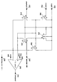
도 2를 보면, 본 개시의 특정 예시의 실시예에 따른, 감지 증폭기를 구비한 셀프 바이어싱 멀티-기준의 개략적인 다이어그램이 도시되어 있다. 트랜지스터들(202, 204, 208, 210, 214 및 218)은 도 2에 도시된 바와 같이 배열되고 함께 연결된 P형 금속 산화막 반도체(PMOS) 트랜지스터들로서, 다음과 같이 상호 기능할 수 있다: 비트 라인(230)에 연결된 EEPROM 메모리 어레이(미도시됨)의 모든 메모리 셀들이 디-어서트될 때에는, nsample 노드(232)에 로직 로우("0")를 어서트하여 트랜지스터(210)를 통해 트랜지스터(204)의 게이트와 드레인이 연결됨으로써, 비트 라인(230)의 전류가 감지된다. 전류는 이후 트랜지스터(204)를 통해 흐르고, 이에 의해, 트랜지스터(214)의 게이트-소스의 양단 간의 전압을 생성하며, 여기서 트랜지스터(214)는 또한 이 전압에 대한 "홀드" 커패시터로서도 기능한다. N형 금속 산화막 반도체(NMOS) 트랜지스터들이 PMOS 트랜지스터들 대신에 사용될 수 있으며, 또한 반도체와 메모리 회로 설계 분야의 당업자와 본 발명의 이익을 가진 자라면 NMOS 트랜지스터들을 사용하여 이러한 회로를 설계할 수 있음이 예상될 수 있고 본 개시의 범위 내에 있다.Turning to Fig. 2, a schematic diagram of a self-biasing multi-reference with sense amplifier is shown, in accordance with an embodiment of a specific example of the present disclosure. The
nsample 노드(232)가 로직 하이("1")로 디-어서트될 때에는, 트랜지스터(204)는 이제 전류 기준으로서 작용하며, 여기서 기준 전류는 "홀드" 커패시터로서 작용하는 트랜지스터(214)의 게이트-소스 양단에 저장된 전압에 의해 결정된다. 그리고 기준 전류는 비트 라인 노드(230)에 연결되는 단일 어서트된 메모리 셀(미도시됨)의 판독 동작 동안 상기 어서트된 메모리 셀로부터의 전류와 비교될 수 있다. 이 어서트된 메모리 셀로부터의 전류에 의존하여 비트 라인 노드(230)에 나타나는 전압은 이 어서트된 메모리 셀의 ON(고전류) 또는 OFF(저전류) 상태에 근거하여 그의 로직 상태를 변경하는 것으로 관측될 수 있다(예를 들어 비트 라인 노드(230)는 기준 전류값이 어서트된 메모리 셀 전류값보다 크면 제1 전압 레벨에 있고, 기준 전류값이 어서트된 메모리 셀 전류값보다 작으면 제2 전압 레벨에 있음). 감지 증폭기(242)는 트랜지스터(204)의 게이트 단자에 나타나는 전압을 그의 기준 입력값으로 재사용함으로써, 비트 라인 노드(230)의 전압 레벨을 검출하는데 사용된다. 감지 증폭기(242)는 Ext.bias 노드(248)로 표시된 외부 바이어스부와 en 노드(246)로 표시된 외부 상태 제어부를 활용하며, 여기서 en 노드(246)는 로직 하이로 어서트될 때 판독 동작을 위해 감지 증폭기(242)를 인에이블하는데 사용되고 그리고 디어서트될 때 감지 증폭기(242)를 디스에이블하는데 사용된다. compout 노드(244)는 감지 증폭기(242)의 출력부로서 비트 라인 노드(230) 전압과 트랜지스터(204)의 게이트 단자에 나타나는 전압 간의 전압 비교의 결과들을 모니터링 하기 위한 수단이다. 트랜지스터(204)의 게이트 단자에 나타나는 전압은, 전압 비교 동작을 위한 기준값으로서 그리고 비트 라인 전류 비교 동작에 활용되는 기준값을 생성하는데 이용되는 저장된 전압 바이어스로서 둘 다 이용되기 때문에 멀티-기준으로 기능을 한다. 이 동작은 비트 라인 노드(230)에 연결되는 메모리 셀들의 수와 무관한데, 그 이유는 관측된 전류 변화가 이하에서 보다 상세하게 설명되듯이, 어서트되고 있는 단일 메모리 셀의 상태 변화에 의해 일어나기 때문이다. When the
nreset 노드(234)가 로직 로우로 어서트될 때에는 트랜지스터(208)는 전력 사이클링 동안에 트랜지스터(204)의 게이트 단자를 방전시켜 vppin 노드(236)에 존재하는 VDD 전위가 되게 하는데 사용될 수 있거나 또는 판독 동작을 시작하고/끝내기 위해 사용될 수 있다. 트랜지스터(218)는 노드(240)의 샘플 신호와 연동하여 디-어서팅 트랜지스터(210)로부터 생기는 "홀드" 단계 전압을 오프셋하는 충전 보상으로서 사용될 수 있다. 이는 트랜지스터(204)에 의해 생성되는 기준 전류가 메모리 어레이 비트 라인 노드(230)에 원래(originally) 존재했던 전류와 같거나 또는 크다는 것을 보증하기 위해 요구될 수 있다. 본 개시의 특정 예시의 실시예에 따라, 트랜지스터(214)의 게이트-소스를 포함하는 '홀드' 커패시터는 실제 커패시터를 사용함으로써 대안으로 제공될 수 있다는 점에 주목해야 한다. Ext.bias 노드(248)과 en 노드(246)의 제어 신호들은 각각 감지 증폭기(242)를 바이어스하고 인에이블하는데 사용된다.
도 3을 보면, 도 2에 도시된 셀프 바이어싱 멀티-기준을 이용하는 회로를 모델링하기 위해 사용된 개략적인 다이어그램이 도시되어 있다. 전류원(446)은 비트 라인 노드(230)에 연결되는 다른 회로 블록들(미도시됨)에 의해 생성되는 누설 전류를 포함시키기(include) 위해 사용된다. 트랜지스터(448)는 비트 라인 노드(230)에 연결되는 디-어서트된 메모리 셀들의 과잉을 포함시키기 위해 사용될 수 있다. 트랜지스터(450)는 판독 동작 동안 wl 노드(452)에 의해 어서트되는 비트 라인 노드(230)에 연결되는 단일 메모리 셀을 나타낸다. 커패시터(454)는 비트 라인 노드(230)과 연관된 부유 커패시턴스를 포함시키기 위해 사용된다. Referring to FIG. 3, there is shown a schematic diagram used to model a circuit using the self-biasing multi-reference shown in FIG. The
도 4를 보면, 어서트된 메모리 셀의 "온" 상태와 "오프" 상태 둘 다에 대해 도 3에 도시된 회로 모델과 연관된 판독 동작 타이밍 파형들이 도시되어 있다. 판독 동작은 nreset 노드(234)가 로직 로우로 잠시 어서트될 때 시작하며, 여기서 nreset 노드(234)에의 로직 로우 어서트는 트랜지스터(204)의 게이트 단자를 vppin 노드(236)에 존재하는 VDD 전위로 방전시킨다. 이것은 또한 트랜지스터(214)의 게이트 단자에 존재하는 임의의 저장된 전하를 방전시키는 역활도 한다. 판독 동작은 nsample 노드(232)와 샘플 노드(240)를 사이클링함으로써 계속되며, 이로 인해, 결과적으로 트랜지스터(214)의 게이트 단자에 나타나는 저장된 전하에 의해 결정된 대로 전류 Istore가 트랜지스터(204)에 생성된다. Istore의 값은 대략 다음과 같을 수 있다.Turning now to FIG. 4, read operation timing waveforms associated with the circuit model shown in FIG. 3 are shown for both the "on" and "off" states of an asserted memory cell. The read operation begins when
Istore ~ I446 + I448 + I450, 디-어서트됨 I store ~ I 446 + I 448 + I 450, de-asserted
또한, 이로 인해, 결과적으로 비트 라인 노드(230)는, 강제로 트랜지스터(204)에 존재하는 게이트-소스 전압에 의해 결정된 대로, vppin 노드(236)에 존재하는 VDD 전위 미만의 전압으로 된다. nsample 노드(232)와 샘플 노드(240)의 사이클링이 완료되면, 메모리 셀 트랜지스터(450)를 어서트하는 wl 노드(452)가 천이된다. 메모리 셀 트랜지스터(450)가 어서트되면, 비트 라인 노드(230)는 이제 2개의 방법들 중 어느 하나에 응답할 것이다:This in turn results in
1) 메모리 셀 트랜지스터(450)이 "오프" 상태에 있다면, 그 때는 비트 라인 노드(230)는 Istore > I446 + I448 + I450, 어서트됨 라는 사실에 근거하여 변화 없이(거의 Vdd 전위임) 유지될 것이다. 그 결과로서, 비트 라인 노드(230) 전압이 트랜지스터(204)의 게이트 단자에 나타나는 기준 전압과 비교되면, 감지 증폭기(242)의 출력, 즉 compout 노드(244)는 로직 로우 상태일 것이다. 1) If the
2) 메모리 셀 트랜지스터(450)이 "온" 상태에 있다면, 그 때는 비트 라인 노드(230)는 Istore < I446 + I448 + I450, 어서트됨 라는 사실에 근거하여 방전(예를 들어, 거의 그라운드 전위임)될 것이다. 그 결과로서, 비트 라인 노드(230) 전압이 트랜지스터(204)의 게이트 단자에 나타나는 기준 전압과 비교되면, 감지 증폭기(242)의 출력, 즉 compout 노드(244)는 로직 하이 상태일 것이다. 2) If the
그러므로, 메모리 셀 트랜지스터(450)의 "온" 또는 "오프" 상태는 감지 증폭기(242)의 출력부, 즉 compout 노드(244)를 모니터링함으로써 용이하게 결정될 수 있다. 판독 동작은, wl 노드(452)를 천이시키고 또한 en 노드(246)를 디어서팅하여 감지 증폭기(242)를 디스에이블링함으로써(도 4에 미도시됨) 메모리 셀 트랜지스터(450)가 디-어서트될 때에 종료된다. Therefore, the "on" or "off" state of the
도 5를 보면, 본 개시의 특정 예시의 실시예에 따른, 셀프 바이어싱 멀티-기준을 활용하는 회로와 연관된 흐름도가 도시되어 있다. 단계 750에서, 제1 비트 라인 전류가 비트 라인에 결합된 모든 메모리 셀들이 디-어서트될 때에 감지된다. 단계 752에서, 감지된 제1 비트 라인 전류가 전압으로 변환되고, 단계 754에서, 전압은 전압 저장 커패시터로서 동작하는 예를 들어, 트랜지스터(214)의 게이트-소스 접합에 저장된다. 단계 756에서, 기준 전류가 저장된 전압에 근거하여 제공된다. 단계 758에서, 저장된 전압은 감지 증폭기를 위한 기준값으로 사용된다. 단계 760에서, 판독 동작 동안, 기준 전류는 기준 전압을 활용하는 감지 증폭기에서 비트 라인에 결합되는 단일 메모리 셀이 어서트될 때의 제2 비트 라인 전류와 비교된다. 단계 762에서, 단일 메모리 셀에 저장된 비트값 충전 상태를 결정하기 위해 비트 라인의 로직 상태가 변화되는지가 감지 증폭기 출력으로부터 결정된다.Turning now to Fig. 5, a flow diagram associated with a circuit utilizing a self-biasing multi-reference, according to an embodiment of a specific example of the present disclosure, is shown. At
본 개시의 교시에 따르면, EEPROM 어레이에서 데이터를 적절하게 판독하기 위해, 현존하는 해결책들의 한계들을 효과적으로 제거하는 "셀프-바이어스된" 멀티-기준이 생성될 수 있다. 공급 전압보다 더 낮은 프리챠지 전압의 사용으로 인해, 전력 소비를 줄일 수 있다. 본 개시의 다양한 실시예들은 제조 비용을 줄이고, 예를 들어(한정하는 것은 아님), 직렬 EEPROM 제조물들과 같은 메모리 디바이스들을 더 강인하게 하는데 사용될 수 있다.According to the teachings of the present disclosure, a "self-biased" multi-reference can be generated that effectively eliminates the limitations of existing solutions to properly read data in an EEPROM array. Due to the use of a precharge voltage that is lower than the supply voltage, power consumption can be reduced. Various embodiments of the present disclosure may be used to reduce manufacturing costs and to make memory devices such as, for example, but not limited to, serial EEPROM manufactures more robust.
본 개시의 실시예들은 본 개시의 예시적인 실시예들을 참조하여 특별히 도시되고 설명되고 정의되었지만, 이러한 참조는 본 개시의 한정을 의미하지 않고 이러한 한정이 추정되지도 않는다. 개시된 본 발명은 이 기술분야에 통상의 기술을 가지고 본 개시의 혜택을 갖는 사람들에게는 형태와 기능에 있어서 상당한 수정, 대체, 및 균등물들이 가능하다. 본 개시의 도시되고 설명된 실시예들은 단지 예로서, 본 개시의 범위를 한정하지 않는다. While the embodiments of the present disclosure have been particularly shown, described and / or defined in connection with the exemplary embodiments of the present disclosure, such references are not meant to imply a limitation of the disclosure and are not intended to be limiting. The disclosed invention is susceptible to numerous modifications, substitutions, and equivalents in form and function to those having ordinary skill in the art and having the benefit of this disclosure. The illustrated and described embodiments of the present disclosure are by way of example only and do not limit the scope of the present disclosure.
Claims (25)
비트 라인에 결합된 모든 메모리 셀들이 디-어서트(de-assert)될 때 상기 비트 라인의 제1 전류값을 감지하는 단계;
상기 제1 전류값을 전압값으로 변환하는 단계;
상기 전압값을 저장하는 단계;
상기 저장된 전압값에 근거한 기준 전류값을 제공하는 단계;
감지 증폭기에 입력으로 사용될 전압 기준값을 상기 저장된 전압값으로부터 제공하는 단계;
상기 비트 라인에 연결된 단일 메모리 셀의 판독 동작 동안에, 감지 증폭기에서 상기 기준 전류값과 상기 단일 메모리 셀이 어서트될 때의 상기 비트 라인의 제2 전류값을 비교하는 단계; 및
상기 기준 전류값과 상기 제2 전류값의 비교로부터의 상기 단일 메모리 셀에 저장된 비트값 충전 상태를 상기 감지 증폭기 출력으로 결정하는 단계를 포함하는, 플로팅 게이트를 구비한 메모리 셀의 충전 상태를 결정하기 위한 방법.A method for determining a state of charge of a memory cell having a floating gate,
Sensing a first current value of the bit line when all memory cells coupled to the bit line are de-asserted;
Converting the first current value to a voltage value;
Storing the voltage value;
Providing a reference current value based on the stored voltage value;
Providing a voltage reference value to be used as an input to the sense amplifier from the stored voltage value;
Comparing the reference current value at a sense amplifier with a second current value of the bit line when the single memory cell is asserted during a read operation of a single memory cell coupled to the bit line; And
Determining a bit value charging state stored in the single memory cell from the comparison of the reference current value and the second current value to the sense amplifier output, determining a state of charge of the memory cell with the floating gate Way.
상기 제1 전류값을 감지하는 단계는, 상기 비트 라인에 결합된 모든 메모리 셀들이 디-어서트될 때, 상기 비트 라인에 제1 트랜지스터의 게이트 및 드레인을 결합시키는 단계를 포함하는, 플로팅 게이트를 구비한 메모리 셀의 충전 상태를 결정하기 위한 방법. The method according to claim 1,
Wherein sensing the first current value comprises coupling a gate and a drain of a first transistor to the bit line when all memory cells coupled to the bit line are de-asserted. A method for determining the state of charge of a provided memory cell.
상기 제1 전류값을 상기 전압값으로 변환하는 단계는, 상기 감지된 제1 전류값으로부터 상기 제1 트랜지스터의 상기 게이트와 소스의 양단 간의 전압을 생성하는 단계를 포함하는, 플로팅 게이트를 구비한 메모리 셀의 충전 상태를 결정하기 위한 방법. 3. The method of claim 2,
Wherein the step of converting the first current value to the voltage value comprises generating a voltage between the gate and source of the first transistor from the sensed first current value, A method for determining the state of charge of a cell.
상기 전압을 저장하는 단계는, 제2 트랜지스터의 게이트와, 함께 연결된 소스-드레인의 양단 간의 전압을 결합시키는 단계를 포함하고, 상기 전압은 상기 제2 트랜지스터의 게이트와 소스-드레인 사이에 형성된 커패시턴스에 저장되는, 플로팅 게이트를 구비한 메모리 셀의 충전 상태를 결정하기 위한 방법. The method of claim 3,
The step of storing the voltage includes coupling a voltage between a gate of the second transistor and a source-drain connected together, and the voltage is applied to a capacitance formed between the gate and the source-drain of the second transistor A method for determining a charged state of a memory cell having a floating gate to be stored.
상기 전압을 저장하는 단계는, 커패시터 양단 간의 전압을 결합시키는 단계를 포함하는, 플로팅 게이트를 구비한 메모리 셀의 충전 상태를 결정하기 위한 방법. The method of claim 3,
Wherein storing the voltage comprises coupling a voltage across the capacitor. ≪ Desc / Clms Page number 21 >
상기 기준 전류값을 제공하는 단계는, 상기 제2 트랜지스터에 저장된 상기 전압에 근거하여 상기 제1 트랜지스터에서 상기 기준 전류값을 생성하는 단계를 포함하는, 플로팅 게이트를 구비한 메모리 셀의 충전 상태를 결정하기 위한 방법. 5. The method of claim 4,
Wherein the step of providing the reference current value comprises the step of generating the reference current value in the first transistor based on the voltage stored in the second transistor, determining the state of charge of the memory cell having the floating gate Lt; / RTI >
상기 기준 전류값을 제공하는 단계는, 상기 커패시터에 저장된 상기 전압에 근거하여 상기 제1 트랜지스터에서 상기 기준 전류값을 생성하는 단계를 포함하는, 플로팅 게이트를 구비한 메모리 셀의 충전 상태를 결정하기 위한 방법. 6. The method of claim 5,
Wherein the step of providing the reference current value comprises generating the reference current value in the first transistor based on the voltage stored in the capacitor. Way.
상기 기준 전류값과 상기 제2 전류값을 비교하는 단계는, 상기 메모리 셀이 어서트 된 후에 상기 메모리 셀과 연관된 상기 비트 라인의 전압을 모니터링하는 단계를 포함하는, 플로팅 게이트를 구비한 메모리 셀의 충전 상태를 결정하기 위한 방법. The method according to claim 1,
Wherein comparing the reference current value to the second current value comprises monitoring the voltage of the bit line associated with the memory cell after the memory cell is asserted. A method for determining a state of charge.
상기 단일 메모리 셀에 저장된 상기 비트값 충전 상태를 결정하는 단계는, 상기 어서트된 메모리 셀과 연관된 상기 비트 라인에 있는 단일 메모리 셀의 로직 상태 또는 부족의 변화를 검출하는 단계를 포함하는, 플로팅 게이트를 구비한 메모리 셀의 충전 상태를 결정하기 위한 방법. The method according to claim 1,
Wherein determining the bit value charged state stored in the single memory cell comprises detecting a change in logic state or deficiency of a single memory cell in the bit line associated with the asserted memory cell, Wherein the method comprises the steps of:
상기 제1 트랜지스터의 상기 드레인은 상기 비트 라인에 결합되고, 상기 제1 트랜지스터의 상기 소스는 전력 공급 전압에 결합되고, 그리고 상기 제2 트랜지스터에 저장된 상기 전압은 상기 기준 전류값을 제공하도록 상기 제1 트랜지스터를 바이어싱하는, 플로팅 게이트를 구비한 메모리 셀의 충전 상태를 결정하기 위한 방법. The method according to claim 6,
Wherein the drain of the first transistor is coupled to the bit line, the source of the first transistor is coupled to a power supply voltage, and the voltage stored in the second transistor is coupled to the first A method for determining the state of charge of a memory cell having a floating gate, the transistor biasing.
상기 어서트된 메모리 셀의 판독 동작 동안, 상기 비트 라인에 결합되는 상기 어서트된 메모리 셀의 비트값 충전 상태를 감지하기 위한 기준 전류값을 결정할 때 상기 제2 트랜지스터의 상기 저장된 전압값이 사용되는, 플로팅 게이트를 구비한 메모리 셀의 충전 상태를 결정하기 위한 방법. The method according to claim 1,
During the read operation of the asserted memory cell, the stored voltage value of the second transistor is used when determining a reference current value for sensing a bit value charging state of the asserted memory cell coupled to the bit line A method for determining the state of charge of a memory cell having a floating gate.
상기 어서트된 메모리 셀의 판독 동작 동안, 상기 제2 트랜지스터에 상기 저장된 전압값이 상기 비트 라인에 결합되는 상기 어서트된 메모리 셀의 비트값 충전 상태를 결정하는 출력부를 갖는 상기 감지 증폭기의 기준 입력으로 재사용되는, 플로팅 게이트를 구비한 메모리 셀의 충전 상태를 결정하기 위한 방법.The method according to claim 1,
Wherein during a read operation of the asserted memory cell a reference value of the sense amplifier having an output for determining a bit value charging state of the asserted memory cell to which the stored voltage value is coupled to the bit line, The method comprising the steps of: determining a state of charge of a memory cell having a floating gate;
상기 제1 트랜지스터 및 상기 제2 트랜지스터는 p형 금속 산화막 반도체(PMOS) 트랜지스터들인, 플로팅 게이트를 구비한 메모리 셀의 충전 상태를 결정하기 위한 방법. 5. The method of claim 4,
Wherein the first transistor and the second transistor are p-type metal oxide semiconductor (PMOS) transistors.
상기 제1 트랜지스터 및 상기 제2 트랜지스터는 n형 금속 산화막 반도체(NMOS) 트랜지스터들인, 플로팅 게이트를 구비한 메모리 셀의 충전 상태를 결정하기 위한 방법. 5. The method of claim 4,
Wherein the first transistor and the second transistor are n-type metal oxide semiconductor (NMOS) transistors.
비트 라인에 결합된 모든 메모리 셀들이 디-어서트될 때, 상기 비트 라인에 결합되는 게이트 및 드레인과 전력 공급 전압에 결합되는 소스를 갖는 제1 트랜지스터, -상기 비트 라인의 제1 전류가 감지됨-; 및
전압값을 저장하는 제2 트랜지스터를 포함하고,
상기 제1 트랜지스터는 상기 제1 전류값을 상기 전압값으로 변환하고;
상기 제1 트랜지스터는 상기 제2 트랜지스터로부터의 상기 저장된 전압값에 근거한 기준 전류값을 제공하고;
상기 커패시터로부터의 저장된 전압이 또한 감지 증폭기의 기준 입력으로 사용되고;
상기 비트 라인에 연결된 단일 메모리 셀의 판독 동작 동안에, 상기 기준 전류값이, 상기 감지 증폭기에서 상기 단일 메모리 셀이 어서트될 때의 상기 비트 라인의 제2 전류값과 비교되고; 그리고
상기 단일 메모리 셀에 저장된 비트값 충전 상태가 상기 기준 전류값과 상기 제2 전류값을 비교하는 상기 감지 증폭기로부터 결정되는, 플로팅 게이트를 구비한 메모리 셀의 충전 상태를 결정하기 위한 장치. An apparatus for determining a state of charge of a memory cell having a floating gate,
A first transistor having a gate and a drain coupled to the bit line and a source coupled to a power supply voltage when all memory cells coupled to the bit line are de-asserted, -; And
And a second transistor for storing a voltage value,
The first transistor converts the first current value to the voltage value;
The first transistor providing a reference current value based on the stored voltage value from the second transistor;
The stored voltage from the capacitor is also used as a reference input of the sense amplifier;
During a read operation of a single memory cell coupled to the bit line, the reference current value is compared to a second current value of the bit line when the single memory cell is asserted in the sense amplifier; And
Wherein a bit value charging state stored in the single memory cell is determined from the sense amplifier comparing the reference current value and the second current value.
상기 제1 트랜지스터를 통한 상기 제1 전류값는 상기 제1 트랜지스터의 게이트와 소스 사이에 전압을 생성하는, 플로팅 게이트를 구비한 메모리 셀의 충전 상태를 결정하기 위한 장치. 16. The method of claim 15,
Wherein the first current value through the first transistor generates a voltage between a gate and a source of the first transistor.
상기 전압은 상기 제2 트랜지스터의 게이트와 소스-드레인 사이에 형성된 커패시턴스에 저장되는, 플로팅 게이트를 구비한 메모리 셀의 충전 상태를 결정하기 위한 장치. 16. The method of claim 15,
Wherein the voltage is stored in a capacitance formed between the gate and source-drain of the second transistor.
상기 전압은 커패시터에 저장되는, 플로팅 게이트를 구비한 메모리 셀의 충전 상태를 결정하기 위한 장치. 16. The method of claim 15,
Wherein the voltage is stored in a capacitor.
상기 기준 전류값은 상기 어서트된 메모리 셀과 연관된 상기 비트 라인에 의한 상기 제2 전류값과 비교되는, 플로팅 게이트를 구비한 메모리 셀의 충전 상태를 결정하기 위한 장치. 16. The method of claim 15,
Wherein the reference current value is compared to the second current value by the bit line associated with the asserted memory cell.
상기 단일 메모리 셀에 저장된 상기 비트값 충전 상태가 상기 어서트된 메모리 셀과 연관된 상기 비트 라인에 있는 상기 단일 메모리 셀의 로직 상태 또는 부족의 변화를 검출함으로써 결정되는, 플로팅 게이트를 구비한 메모리 셀의 충전 상태를 결정하기 위한 장치. 16. The method of claim 15,
Wherein the bit value charged state stored in the single memory cell is determined by detecting a logic state or a lack of a change in the single memory cell in the bit line associated with the asserted memory cell. An apparatus for determining a state of charge.
상기 제1 트랜지스터의 드레인은 상기 비트 라인에 결합되고, 상기 제1 트랜지스터의 소스는 전력 공급 전압에 결합되고, 그리고 상기 제2 트랜지스터에 상기 저장된 전압은 상기 기준 전류를 제공하기 위해 제1 트랜지스터를 바이어싱하는, 플로팅 게이트를 구비한 메모리 셀의 충전 상태를 결정하기 위한 장치. 16. The method of claim 15,
Wherein a drain of the first transistor is coupled to the bit line, a source of the first transistor is coupled to a power supply voltage, and a voltage stored in the second transistor is coupled to a first transistor, Wherein the charging state of the memory cell having the floating gate is determined.
상기 어서트된 메모리 셀의 판독 동작 동안에, 상기 제2 트랜지스터에 상기 저장된 전압값은 상기 비트 라인에 결합되는 상기 어서트된 메모리 셀의 비트값 충전 상태를 결정하는 출력부를 갖는 상기 감지 증폭기의 기준 입력으로 제공되는, 플로팅 게이트를 구비한 메모리 셀의 충전 상태를 결정하기 위한 장치.16. The method of claim 15,
Wherein during a read operation of the asserted memory cell, the stored voltage value at the second transistor is a reference input of the sense amplifier having an output for determining a bit value charged state of the asserted memory cell coupled to the bit line Wherein the charge state of the memory cell comprises a floating gate.
상기 제1 트랜지스터 및 상기 제2 트랜지스터는 p형 금속 산화막 반도체(PMOS) 트랜지스터들인, 플로팅 게이트를 구비한 메모리 셀의 충전 상태를 결정하기 위한 장치. 16. The method of claim 15,
Wherein the first transistor and the second transistor are p-type metal oxide semiconductor (PMOS) transistors.
상기 제1 트랜지스터 및 상기 제2 트랜지스터는 n형 금속 산화막 반도체(NMOS) 트랜지스터들인, 플로팅 게이트를 구비한 메모리 셀의 충전 상태를 결정하기 위한 장치. 16. The method of claim 15,
Wherein the first transistor and the second transistor are n-type metal oxide semiconductor (NMOS) transistors.
비트 라인에 결합된 모든 메모리 셀들이 디-어서트될 때, 상기 비트 라인에 결합되는 게이트 및 드레인과, 전력 공급 전압에 결합되는 소스를 갖는 제1 트랜지스터, -상기 비트 라인의 제1 전류가 감지됨-; 및
전압값을 저장하는 커패시터를 포함하고,
상기 제1 트랜지스터는 상기 제1 전류값을 상기 전압값으로 변환하고;
상기 제1 트랜지스터는 상기 커패시터부터의 상기 저장된 전압값에 근거한 기준 전류값을 제공하고;
상기 커패시터로부터의 저장된 전압이 또한 감지 증폭기의 기준 입력으로 사용되고;
상기 비트 라인에 연결된 단일 메모리 셀의 판독 동작 동안에, 상기 기준 전류값이, 상기 감지 증폭기에서 상기 단일 메모리 셀이 어서트될 때의 상기 비트 라인의 제2 전류값과 비교되고; 그리고
상기 단일 메모리 셀에 저장된 비트값 충전 상태가 상기 기준 전류값과 상기 제2 전류값을 비교하는 상기 감지 증폭기로부터 결정되는, 플로팅 게이트를 구비한 메모리 셀의 충전 상태를 결정하기 위한 장치. An apparatus for determining a state of charge of a memory cell having a floating gate,
A first transistor having a gate and a drain coupled to the bit line and a source coupled to a power supply voltage when all memory cells coupled to the bit line are de-asserted, being-; And
A capacitor for storing a voltage value,
The first transistor converts the first current value to the voltage value;
The first transistor providing a reference current value based on the stored voltage value from the capacitor;
The stored voltage from the capacitor is also used as a reference input of the sense amplifier;
During a read operation of a single memory cell coupled to the bit line, the reference current value is compared to a second current value of the bit line when the single memory cell is asserted in the sense amplifier; And
Wherein a bit value charging state stored in the single memory cell is determined from the sense amplifier comparing the reference current value and the second current value.
Applications Claiming Priority (5)
| Application Number | Priority Date | Filing Date | Title |
|---|---|---|---|
| US201261702391P | 2012-09-18 | 2012-09-18 | |
| US61/702,391 | 2012-09-18 | ||
| US14/029,616 US9129680B2 (en) | 2012-09-18 | 2013-09-17 | Self-biasing multi-reference |
| US14/029,616 | 2013-09-17 | ||
| PCT/US2013/060310 WO2014047119A1 (en) | 2012-09-18 | 2013-09-18 | Self-biasing multi-reference for sensing memory cell |
Publications (1)
| Publication Number | Publication Date |
|---|---|
| KR20150056845A true KR20150056845A (en) | 2015-05-27 |
Family
ID=50274324
Family Applications (1)
| Application Number | Title | Priority Date | Filing Date |
|---|---|---|---|
| KR1020157009900A KR20150056845A (en) | 2012-09-18 | 2013-09-18 | Self-biasing multi-reference for sensing memory cell |
Country Status (6)
| Country | Link |
|---|---|
| US (1) | US9129680B2 (en) |
| EP (1) | EP2898511A1 (en) |
| JP (1) | JP2015531958A (en) |
| KR (1) | KR20150056845A (en) |
| CN (1) | CN104685568B (en) |
| WO (1) | WO2014047119A1 (en) |
Families Citing this family (6)
| Publication number | Priority date | Publication date | Assignee | Title |
|---|---|---|---|---|
| KR102166913B1 (en) * | 2014-01-03 | 2020-10-16 | 삼성전자주식회사 | Self bias buffer circuit and memory device including the same |
| US9142271B1 (en) * | 2014-06-24 | 2015-09-22 | Intel Corporation | Reference architecture in a cross-point memory |
| US9947389B1 (en) * | 2016-11-30 | 2018-04-17 | Taiwan Semiconductor Manufacturing Co., Ltd. | Single ended memory device |
| US10304514B2 (en) | 2017-07-05 | 2019-05-28 | Micron Technology, Inc. | Self-reference sensing for memory cells |
| US10395715B2 (en) | 2017-08-25 | 2019-08-27 | Micron Technology, Inc. | Self-referencing memory device |
| US10475510B2 (en) | 2017-12-21 | 2019-11-12 | Macronix International Co., Ltd. | Leakage compensation read method for memory device |
Family Cites Families (8)
| Publication number | Priority date | Publication date | Assignee | Title |
|---|---|---|---|---|
| US6052307A (en) * | 1998-08-11 | 2000-04-18 | Texas Instruments Incorporated | Leakage tolerant sense amplifier |
| US6407946B2 (en) * | 1999-12-08 | 2002-06-18 | Matsushita Electric Industrial Co., Ltd. | Nonvolatile semiconductor memory device |
| US6891768B2 (en) | 2002-11-13 | 2005-05-10 | Hewlett-Packard Development Company, L.P. | Power-saving reading of magnetic memory devices |
| KR100587694B1 (en) * | 2005-02-16 | 2006-06-08 | 삼성전자주식회사 | Semiconductor memory device capable of compensating for leakage current |
| FR2888659A1 (en) * | 2005-07-18 | 2007-01-19 | St Microelectronics Sa | PLAY AMPLIFIER FOR NON-VOLATILE MEMORY |
| KR100781984B1 (en) * | 2006-11-03 | 2007-12-06 | 삼성전자주식회사 | Sense amplifier circuit having self reference and sensing method by the same |
| US8467253B2 (en) | 2010-05-24 | 2013-06-18 | Hewlett-Packard Development Company, L.P. | Reading memory elements within a crossbar array |
| US9129695B2 (en) * | 2012-09-18 | 2015-09-08 | Microchip Technology Incorporated | Self-biasing current reference |
-
2013
- 2013-09-17 US US14/029,616 patent/US9129680B2/en active Active
- 2013-09-18 JP JP2015532160A patent/JP2015531958A/en not_active Ceased
- 2013-09-18 EP EP13770774.1A patent/EP2898511A1/en not_active Withdrawn
- 2013-09-18 CN CN201380050582.8A patent/CN104685568B/en not_active Expired - Fee Related
- 2013-09-18 KR KR1020157009900A patent/KR20150056845A/en not_active Application Discontinuation
- 2013-09-18 WO PCT/US2013/060310 patent/WO2014047119A1/en active Application Filing
Also Published As
| Publication number | Publication date |
|---|---|
| EP2898511A1 (en) | 2015-07-29 |
| US20140078831A1 (en) | 2014-03-20 |
| WO2014047119A1 (en) | 2014-03-27 |
| CN104685568B (en) | 2018-07-31 |
| CN104685568A (en) | 2015-06-03 |
| JP2015531958A (en) | 2015-11-05 |
| US9129680B2 (en) | 2015-09-08 |
Similar Documents
| Publication | Publication Date | Title |
|---|---|---|
| US9129680B2 (en) | Self-biasing multi-reference | |
| JP4579493B2 (en) | Nonvolatile semiconductor memory device and data reading method | |
| US7352618B2 (en) | Multi-level cell memory device and associated read method | |
| US8254178B2 (en) | Self-timed integrating differential current | |
| US7724603B2 (en) | Method and circuit for preventing high voltage memory disturb | |
| KR100893474B1 (en) | Semiconductor memory device | |
| CN108172250A (en) | High speed and low-power sense amplifier | |
| JPH08321194A (en) | Sense amplifier circuit | |
| US7986579B2 (en) | Memory device and method thereof | |
| KR100323324B1 (en) | Semiconductor memory device | |
| CN104751891A (en) | Reading operation time control circuit | |
| US20100027353A1 (en) | Erase Method of Flash Device | |
| US9129695B2 (en) | Self-biasing current reference | |
| CN105225693B (en) | Virtual ground flash memory circuit | |
| JP2003338186A (en) | Semiconductor nonvolatile memory device | |
| US8488370B2 (en) | Differential threshold voltage non-volatile memory and related methods | |
| US20150003168A1 (en) | Non-volatile memory device with improved reading circuit | |
| JP4885743B2 (en) | Nonvolatile semiconductor memory device | |
| US8462565B2 (en) | Differential threshold voltage non-volatile memory and related methods | |
| US8913439B2 (en) | Memory device and corresponding reading method | |
| TWI324774B (en) | Biasing and shielding circuit for source side sensing memory | |
| KR101383104B1 (en) | Sensor amplifier circuit in nonvolatile memory device having improved sensing efficiency | |
| JP2006164382A (en) | Ferroelectric memory device | |
| JP2003085990A (en) | Nonvolatile semiconductor memory |
Legal Events
| Date | Code | Title | Description |
|---|---|---|---|
| WITN | Application deemed withdrawn, e.g. because no request for examination was filed or no examination fee was paid |