KR20150052834A - Fine structure, optical member, antireflection film, water-repellent film, substrate for mass spectrometry, phase plate, process for producing fine structure, and process for producing antireflection film - Google Patents
Fine structure, optical member, antireflection film, water-repellent film, substrate for mass spectrometry, phase plate, process for producing fine structure, and process for producing antireflection film Download PDFInfo
- Publication number
- KR20150052834A KR20150052834A KR1020157002255A KR20157002255A KR20150052834A KR 20150052834 A KR20150052834 A KR 20150052834A KR 1020157002255 A KR1020157002255 A KR 1020157002255A KR 20157002255 A KR20157002255 A KR 20157002255A KR 20150052834 A KR20150052834 A KR 20150052834A
- Authority
- KR
- South Korea
- Prior art keywords
- mesopores
- microstructure
- meso
- protrusions
- film
- Prior art date
Links
Images


Classifications
-
- G—PHYSICS
- G02—OPTICS
- G02B—OPTICAL ELEMENTS, SYSTEMS OR APPARATUS
- G02B1/00—Optical elements characterised by the material of which they are made; Optical coatings for optical elements
- G02B1/10—Optical coatings produced by application to, or surface treatment of, optical elements
- G02B1/11—Anti-reflection coatings
- G02B1/111—Anti-reflection coatings using layers comprising organic materials
-
- G—PHYSICS
- G02—OPTICS
- G02B—OPTICAL ELEMENTS, SYSTEMS OR APPARATUS
- G02B1/00—Optical elements characterised by the material of which they are made; Optical coatings for optical elements
- G02B1/10—Optical coatings produced by application to, or surface treatment of, optical elements
- G02B1/11—Anti-reflection coatings
- G02B1/118—Anti-reflection coatings having sub-optical wavelength surface structures designed to provide an enhanced transmittance, e.g. moth-eye structures
-
- G—PHYSICS
- G02—OPTICS
- G02B—OPTICAL ELEMENTS, SYSTEMS OR APPARATUS
- G02B1/00—Optical elements characterised by the material of which they are made; Optical coatings for optical elements
- G02B1/10—Optical coatings produced by application to, or surface treatment of, optical elements
- G02B1/18—Coatings for keeping optical surfaces clean, e.g. hydrophobic or photo-catalytic films
-
- G—PHYSICS
- G02—OPTICS
- G02B—OPTICAL ELEMENTS, SYSTEMS OR APPARATUS
- G02B27/00—Optical systems or apparatus not provided for by any of the groups G02B1/00 - G02B26/00, G02B30/00
- G02B27/0006—Optical systems or apparatus not provided for by any of the groups G02B1/00 - G02B26/00, G02B30/00 with means to keep optical surfaces clean, e.g. by preventing or removing dirt, stains, contamination, condensation
-
- G—PHYSICS
- G02—OPTICS
- G02B—OPTICAL ELEMENTS, SYSTEMS OR APPARATUS
- G02B2207/00—Coding scheme for general features or characteristics of optical elements and systems of subclass G02B, but not including elements and systems which would be classified in G02B6/00 and subgroups
- G02B2207/107—Porous materials, e.g. for reducing the refractive index
-
- Y—GENERAL TAGGING OF NEW TECHNOLOGICAL DEVELOPMENTS; GENERAL TAGGING OF CROSS-SECTIONAL TECHNOLOGIES SPANNING OVER SEVERAL SECTIONS OF THE IPC; TECHNICAL SUBJECTS COVERED BY FORMER USPC CROSS-REFERENCE ART COLLECTIONS [XRACs] AND DIGESTS
- Y10—TECHNICAL SUBJECTS COVERED BY FORMER USPC
- Y10T—TECHNICAL SUBJECTS COVERED BY FORMER US CLASSIFICATION
- Y10T428/00—Stock material or miscellaneous articles
- Y10T428/24—Structurally defined web or sheet [e.g., overall dimension, etc.]
- Y10T428/24355—Continuous and nonuniform or irregular surface on layer or component [e.g., roofing, etc.]
Landscapes
- Physics & Mathematics (AREA)
- General Physics & Mathematics (AREA)
- Optics & Photonics (AREA)
- Chemical & Material Sciences (AREA)
- Chemical Kinetics & Catalysis (AREA)
- Surface Treatment Of Optical Elements (AREA)
- Oxygen, Ozone, And Oxides In General (AREA)
- Laminated Bodies (AREA)
Abstract
높은 반사방지 효과를 갖는 반사방지막 및 그의 제조 방법, 반사방지 효과가 우수한 광학 부재, 우수한 발수성을 갖는 발수성 막, 높은 검출 감도를 갖는 질량 분석용 기판, 고-정밀도 위상판, 및 이들에 사용될 수 있는 미세구조체 및 그의 제조 방법이 제공된다. 본 발명의 미세구조체는, 그의 표면 상에 복수의 원추부를 포함하며, 여기서, 원추부는 메소구조를 갖고; 메소구조는 메소세공을 갖는 구조를 포함하는, 구조체이다.An antireflection film having high antireflection effect, an optical member having excellent antireflection effect, a water repellent film having excellent water repellency, a mass spectrometry substrate having high detection sensitivity, a high-precision phase plate, A microstructure and a method of manufacturing the same are provided. The microstructure of the present invention includes a plurality of cones on its surface, wherein the cones have a meso structure; The meso structure is a structure comprising a structure having mesopores.
Description
본 발명은 반사방지 재료, 센서, 초-발수성 재료, 및 초-친수성 재료 등의 다양한 용도에서 사용되는 복수의 원추부 또는 돌출부를 갖는 미세구조체, 광학 부재, 반사방지막, 발수성 막, 질량 분석용 기판, 위상판, 및 구조체의 제조 방법, 및 반사방지막의 제조 방법에 관한 것이다.The present invention relates to a microstructure having a plurality of cones or protrusions used in various applications such as antireflection materials, sensors, super-water-repellent materials, and super-hydrophilic materials, optical members, antireflection coatings, water repellent coatings, A phase plate, a method of manufacturing a structure, and a method of manufacturing an antireflection film.
종래, 광 파장보다 작은 스케일의 복수의 미세 돌출부를 갖는 구조체 (이하, "미세구조체"라고도 함)는, 초-발수성 재료, 초-친수성 재료, 전지 재료, 마찰방지 재료, 및 반사방지 재료 등의 다양한 구조 재료로서 사용되었다.Conventionally, a structure (hereinafter also referred to as a " microstructure ") having a plurality of fine protrusions on a scale smaller than the wavelength of light has been widely used in various applications such as an ultra-water repellent material, a super-hydrophilic material, a battery material, It was used as various structural materials.
이러한 광 파장보다 작은 스케일의 복수의 미세 돌출부를 갖는 미세구조체의 제조 방법은 대체로 하기 3개의 방법으로 분류될 수 있다:A method of manufacturing a microstructure having a plurality of fine protrusions on a scale smaller than such a light wavelength can be roughly classified into the following three methods:
(1) 피가공물 상에 마스크로서 작용하는 생성물을 미리 형성한 후, 피가공물을 에칭하는 것을 포함하는 (마스크-배치 단계 및 에칭 단계를 포함하는) 방법;(1) a method (including a mask-disposing step and an etching step) which includes previously forming a product acting as a mask on a workpiece, and then etching the workpiece;
(2) 피가공물을 에칭하는 것을 포함하는 (단지 에칭 단계만을 포함하는) 방법; 및(2) a method (including only an etching step) that involves etching the workpiece; And
(3) 방법 (1), (2) 등에 의해 제조된 미세구조체를 주형으로 하여 피가공물을 전사 성형에 적용하는 것을 포함하는 방법.(3) A method comprising applying a workpiece to a transfer molding using the microstructure produced by the method (1) or (2) as a template.
마스크-배치 단계 및 에칭 단계를 포함하는 종래의 제조예 (1)로서는 주요 리소그래피 기술을 포함하는 반도체 프로세스에 의한 제조가 시도되었다 (특허문헌 3). 방법은, 미세구조체 형성에 사용되는 기판 상에 레지스트를 적용하고; 레지스트를 포토마스크를 통해 노광 및 현상하여 마스크 패턴을 얻고; 마스크 패턴을 에칭에 의해 미세구조체 형성용 기판에 전사하는 것을 포함한다. 리소그래피 기술은 정밀하게 설계된 미세 패턴이 형성될 수 있는 방법으로서 유리하다 (특허문헌 1).As a conventional manufacturing example (1) including a mask-placing step and an etching step, manufacturing by a semiconductor process including a main lithography technique has been attempted (Patent Document 3). The method comprises applying a resist on a substrate used for forming a microstructure; Exposing and developing the resist through a photomask to obtain a mask pattern; And transferring the mask pattern to the substrate for forming a microstructure by etching. The lithography technique is advantageous as a method by which a finely patterned fine pattern can be formed (Patent Document 1).
리소그래피 기술을 이용하지 않고 마스크 패턴을 자발적으로 형성하는 것을 포함하는 기술이 또한 제안되었다. 예를 들어, 기판 상에 배열된 미립자, 섬(island) 형상의 금속 박막 등을 마스크로 하여 광 파장보다 작은 스케일의 미세구조체를 용이하게 제조할 수 있는 기술이 개시되었다 (특허문헌 2 및 3).Techniques involving spontaneously forming mask patterns without using lithographic techniques have also been proposed. For example, there has been disclosed a technique capable of easily fabricating a microstructure having a scale smaller than the wavelength of light using fine particles arranged on a substrate, an island-shaped metal thin film, or the like as a mask (
"단지 에칭 단계만"으로 형성되는 종래의 제조예 (2)로서는 Si 플라즈마 에칭 (반응성 이온 에칭) 공정에서 침상이 형성되는 현상이 공지되어 있고, 재료는 "흑색 규소"라 불린다 (비특허문헌 1).In the conventional production example (2) in which only the "etching step only" is performed, a phenomenon that a needle is formed in the Si plasma etching (reactive ion etching) process is known, and the material is called "black silicon" ).
예를 들어, 미세구조체를 주형으로 하여 전사하는 것을 포함하는 종래의 제조예 (3)로서는, 플라즈마 에칭 장치를 사용하여 형성된 미세한 돌기부를 갖는 탄소 재료를 주형으로 하여 광경화성 수지 등에 미세 돌기 형상을 전사하는 것을 포함하는 방법이 제안되었다 (특허문헌 4).For example, as a conventional production example (3) including transferring using a microstructure as a mold, a microprojection shape is transferred to a photocurable resin or the like using a carbon material having a fine protruding portion formed by using a plasma etching apparatus (Patent Document 4).
특히, 미세구조체에서의 돌출부의 형상이 원추 형상인 경우, 즉, 돌출부가, 그의 저부로부터 그의 첨단을 향하는 방향에 대해 수직인 단면적이 상기 방향을 따라 감소하는 형상을 갖는 경우, 미세구조체는, 예를 들어, 반사방지막, 발수성 막, 초-친수성 막, 질량 분석용 기판, 전지 재료, 또는 마찰방지 재료로서 사용될 수 있다.Particularly, when the shape of the protrusion in the microstructure is conical, that is, when the protrusion has a shape in which the cross-sectional area perpendicular to the direction from the bottom toward the tip of the protrusion has a decreasing shape along the direction, For example, an antireflection film, a water-repellent film, a super-hydrophilic film, a substrate for mass spectrometry, a battery material, or a friction-preventing material.
반사방지막에 관한 기술로서는, 각각 기판의 굴절률과 상이한 굴절률을 갖는 하나 이상의 광학 막을 적층시켜 적층체의 두께가 수십 내지 수백 나노미터가 될 수 있게 함으로써 얻어지는 광 간섭 효과를 이용한 반사 억제를 포함하는 기술이 일반적이다. 광학 막 형성을 위해서는 기상 성막 또는 스퍼터링 등의 진공 성막법, 또는 딥 코팅 또는 스핀 코팅 등의 습식 성막법이 이용된다. 이러한 일반적인 반사방지막은 광선 입사각이 0°이고, 비교적 좁은 파장 영역인 막이 사용되는 파장 영역에서 우수한 반사방지 효과를 갖도록 설계된다. 그러나, 예를 들어, 구경이 큰 렌즈 또는 곡률 반경이 작은 표면을 갖는 렌즈에 사용되는 반사방지막은, 폭넓은 파장 영역에서 우수한 반사방지 기능을 갖고, 광속의 입사각 특성이 우수할 것이 요망된다. 폭넓은 파장 영역에서 이용가능하고, 우수한 입사각 특성을 갖는 반사방지 수단으로서는, 피치가 입사광의 파장보다 짧은 미세구조체 (예를 들어, "서브-파장 구조체 (SWS)" 또는 "나방눈(moth-eye) 구조체"라고 언급됨)의 배열이 공지되어 있다 (특허문헌 5 및 6). 특히, 미세구조체가 첨예화된 구조를 갖는 경우에는, 공간에서 물질에 의해 점유된 부피가 돌출 구조의 상부로부터 그의 하부로 가면서 점차 증가하고, 따라서 계면에서의 급격한 굴절률 변화가 억제된다. 그 결과, 반사가 크게 감소된다.As a technique relating to the antireflection film, a technique including reflection suppression using a light interference effect obtained by laminating at least one optical film having a refractive index different from the refractive index of the substrate so that the thickness of the laminate becomes tens to hundreds of nanometers It is common. In order to form an optical film, a vacuum film formation method such as gas phase film formation or sputtering, or a wet film formation method such as dip coating or spin coating is used. This general antireflection film is designed to have an excellent reflection preventing effect in a wavelength region where a film having a relatively narrow wavelength region and a light incident angle of 0 DEG is used. However, for example, an antireflection film used in a lens having a large aperture or a surface having a small radius of curvature has an excellent antireflection function in a wide wavelength range, and is desired to have excellent incident angle characteristics of the light flux. As the antireflection means which can be used in a wide wavelength range and has a good incident angle characteristic, a microstructure (for example, "sub-wavelength structure (SWS)" or "moth-eye ) Structure ") are known (
표면 상에 복수의 돌출부로 형성된 미세구조체를 갖는 막은 높은 발수성을 나타낸다는 사실은 로터스(lotus) 효과로서 공지되어 있다 (특허문헌 7 및 비특허문헌 2). 돌출부의 형상, 배열, 소수성 개질 기 등의 조건을 적절히 설계함으로써 막 표면에서의 수 액적의 접촉각이 150°를 초과하는 초-발수성이 실현될 수 있다. 이러한 초-발수성을 나타내는 막은, 예를 들어, 각종 광학 부재 및 건축 부재의 표면 코팅에서의 응용이 기대되고 있다.The fact that a film having a microstructure formed of a plurality of protrusions on its surface exhibits high water repellency is known as a lotus effect (Patent Document 7 and Non-Patent Document 2). By appropriately designing the conditions such as the shape, arrangement, and hydrophobic reformer of the protrusions, the super-water repellency in which the contact angle of the water droplet on the surface of the membrane exceeds 150 ° can be realized. Such a film showing super-water repellency is expected to be applied, for example, to surface coating of various optical members and architectural members.
표면 상에 복수의 돌출부로 형성된 미세구조체를 갖는 막은 또한 질량 분석용 기판으로서 사용될 수 있다. 이는, 분석되는 재료를 미세구조를 갖는 반도체 박막 상에 유지시키고, 레이저 또는 이온 빔을 적용하여 구조를 파괴시키지 않고 분석 대상을 이온화시키고, 그의 질량을 고감도로 측정하여 재료의 성분을 규명하는 것을 포함하는 기술이며, 이 기술은 매트릭스-보조 질량 분석과 유사한 표면-보조 레이저 탈착/이온화 질량 분석 (SALDI-MS)로서 공지되어 있다 (특허문헌 8). 기판 표면 상의 미세구조는 주로 이온화에 따른 검체 시료의 파괴를 막는 역할을 하고, 따라서 약 10 nm의 크기를 가질 필요가 있다. 표면-보조 레이저 탈착/이온화 질량 분석에 사용되는 기판으로서는 규소의 애노드화 처리에 의해 제조된 다공성 규소가 가장 일반적이다. 또한, 예를 들어, 공기 중에서의 산화로 인한 다공성 규소의 전기 전도도 저하에 기인하는 특성 열화의 문제를 해결할 수 있는 재료로서, 폴리에틸렌 글리콜을 공존시킴으로써 또는 졸-겔법에 의해 제조된, 표면 상에 미세구조를 갖는 산화티타늄 박막이 제안되었다 (비특허문헌 3). 이에 사용되는 산화티타늄 박막 내에는 약 10 nm의 랜덤 형상의 미세 세공이 존재하고, 이들 미세 세공은 각각 주로 이온화에 따른 검체 시료의 파괴를 막는 역할을 한다.A film having a microstructure formed of a plurality of protrusions on a surface can also be used as a substrate for mass spectrometry. This involves maintaining the material to be analyzed on a semiconductor thin film having a microstructure, ionizing the analyte without destroying the structure by applying a laser or an ion beam, and measuring its mass with high sensitivity to identify the components of the material This technique is known as surface-assisted laser desorption / ionization mass spectrometry (SALDI-MS) similar to matrix-assisted mass spectrometry (Patent Document 8). The microstructure on the surface of the substrate mainly serves to prevent destruction of the specimen due to ionization, and thus it is necessary to have a size of about 10 nm. As substrates used for surface-assisted laser desorption / ionization mass spectrometry, porous silicon produced by anodizing treatment of silicon is the most common. Further, as a material capable of solving the problem of deterioration in characteristics due to, for example, degradation of the electrical conductivity of porous silicon due to oxidation in air, there has been proposed a method in which fine grains are formed on the surface by coexisting polyethylene glycol or by sol- (Non-Patent Document 3). In the titanium oxide thin film used there is a random pores having a size of about 10 nm, and these micro pores mainly prevent destruction of the specimen due to ionization.
발명의 요약SUMMARY OF THE INVENTION
<해결하려는 과제><Challenge to solve>
그러나, 선행 기술은 여러 문제를 포함한다.However, the prior art includes various problems.
먼저, 복수의 돌출부를 갖는 미세구조체의 제조와 관련된 문제는 하기에 기재되는 바와 같다. 피가공물 상에 마스크로서 작용하는 생성물을 미리 형성한 후, 피가공물을 에칭하는 것을 포함하는 방법의 경우에는, 마스크 배열 단계가 필요하고, 따라서 제조 방법이 복잡하고, 미세구조체를 저비용으로 제조하는 것이 어렵다. 또한, 임의의 마스크를 사용하지 않고 단지 에칭만을 포함하는 제조 방법은 하기 문제를 포함한다: 적용가능한 재료의 수가 극히 작기 때문에 그의 용도가 제한된다. 예를 들어, 흑색 규소 또는 미세구조를 갖는 탄소는 이를 통해 가시광이 투과할 수 없기 때문에 렌즈와 같은 부재에 대한 반사방지막으로서 적용될 수 없다. 따라서, 폭넓게 다양한 재료, 특히 폭넓은 밴드 갭을 갖는 투명하고 안정한 재료 상에 임의의 마스크를 사용하지 않고 복수의 원추체-형상의 미세 돌출부를 형성하는 기술이 요구되고 있다.First, the problems associated with the fabrication of microstructures having a plurality of protrusions are as described below. In the case of a method including previously forming a product acting as a mask on a workpiece and then etching the workpiece, a mask arraying step is required, and therefore, a manufacturing method is complicated, and manufacturing a microstructure at a low cost it's difficult. Further, the manufacturing method which includes only etching without using any mask includes the following problems: its application is limited because the number of applicable materials is extremely small. For example, black silicon or carbon having a microstructure can not be applied as an antireflection film to a member such as a lens because it can not transmit visible light therethrough. Therefore, there is a demand for a technique of forming a plurality of conical-shaped micro protrusions on a wide variety of materials, particularly transparent and stable materials having a wide band gap, without using any mask.
또한, 각각의 돌출부의 표면에만 소수성 화학 개질이 제공된, 종래 보고된 발수성 재료 막에서는, 막 표면에 대한 외력 적용으로 인한 돌출부 형상의 파괴시 새로 노출되는 단면부는 임의의 소수성 개질 기를 갖지 않는다. 그 결과, 하기 문제가 발생한다: 막 표면에서 국소적으로 발수성이 현저히 열화되는 개소가 생긴다. 따라서, 파단면이 발생하는 경우에도 발수성이 감소되지 않는 발수성 재료 막이 요구되고 있다.Also, in the previously reported water repellent material membranes provided with hydrophobic chemical modification only on the surface of each protrusion, the cross-section newly exposed at break of the protrusion shape due to external force application to the membrane surface does not have any hydrophobic modifying groups. As a result, the following problems arise: a portion where the water repellency is remarkably deteriorated locally occurs on the film surface. Therefore, a water repellent material film that does not decrease water repellency even when a fractured surface is generated is required.
또한, 표면 상에 미세구조를 갖는 종래의 질량 분석용 기판은 하기 문제를 포함한다. 구조의 크기가 이온화에 사용되는 프로브 (레이저 광 등)의 파장에 비해 현저히 작고, 따라서 막 표면에서의 프로브 광의 반사가 막 내로 주입되는 에너지를 감소시키고, 그 결과, 일부 경우에 이온화 효율이 감소한다. 따라서, 이온화에 따른 검체 시료의 파괴를 막는 역할을 하는 미세한 구조를 유지하면서 반사를 방지할 수 있도록 막의 모폴로지(morphology)를 미세가공에 적용할 수 있는 기술이 요구되고 있다.In addition, conventional mass spectrometry substrates having a microstructure on the surface include the following problems. The size of the structure is significantly smaller than the wavelength of the probe (laser light or the like) used for ionization, thus reducing the energy into which the reflection of the probe light at the film surface is injected into the film, and as a result, the ionization efficiency is reduced in some cases . Therefore, there is a demand for a technique capable of applying a morphology of a film to microfabrication so as to prevent reflections while maintaining a fine structure that serves to prevent the specimen from destruction due to ionization.
본 발명의 추가의 특징은, 첨부된 도면을 참조로 하여 하기 예시적 실시양태의 설명으로부터 명백해질 것이다.Further features of the present invention will become apparent from the following description of exemplary embodiments with reference to the accompanying drawings.
<과제의 해결 수단>MEANS FOR SOLVING THE PROBLEMS [
본 발명의 예시적 실시양태는, 표면 상에 복수의 원추부를 포함하며, 여기서 원추부는 메소구조를 갖고; 메소구조는 메소세공을 갖는 구조를 포함하는 것인, 미세구조체에 관한 것이다.An exemplary embodiment of the present invention includes a plurality of cones on a surface, wherein the cones have a meso structure; Wherein the meso structure comprises a structure having mesopores.
본 발명의 또 다른 예시적 실시양태는, 표면 상에 복수의 돌출부를 포함하며, 여기서, 돌출부는, 돌출부가 돌출부의 저부로부터 그의 첨단을 향하는 방향에 대해 수직인 면으로 절단될 때 단면적이 상기 방향을 따라 감소하는 형상을 갖고; 돌출부가 메소세공을 갖는 메소구조를 갖고; 돌출부의 첨단에 금속 원소가 존재하고; 돌출부의 저변의 길이를 D로 나타내고, 돌출부의 높이를 H로 나타낼 때, H/D 비율이 2.0 이상인, 미세구조체에 관한 것이다.Another exemplary embodiment of the present invention is a semiconductor device including a plurality of protrusions on a surface, wherein the protrusions have a cross-sectional area when the protrusions are cut into a plane perpendicular to the direction from the bottom of the protrusions toward the tip of the protrusions, Has a shape decreasing along the axis; The protrusions having a meso structure with mesopores; A metal element is present at the tip of the protrusion; And the H / D ratio is not less than 2.0 when the height of the protruding portion is denoted by H. The present invention relates to a microstructure.
본 발명의 또 다른 예시적 실시양태는, 표면 상에 복수의 돌출부를 갖는 미세구조체를 포함하며, 여기서, 돌출부는 각각 메소구조를 갖고; 메소구조는 메소세공을 갖는 구조이고; 돌출부는, 돌출부가 돌출부의 저부로부터 그의 첨단을 향하는 방향에 대해 수직인 면으로 절단될 때 단면적이 상기 방향을 따라 감소하는 형상을 갖는 것인, 반사방지막에 관한 것이다.Another exemplary embodiment of the present invention includes a microstructure having a plurality of protrusions on a surface, wherein the protrusions each have a meso structure; The meso structure is a structure having mesopores; Wherein the projection has a shape in which the cross-sectional area decreases along the direction when the projection is cut into a plane perpendicular to the direction from the bottom of the projection toward the tip of the projection.
본 발명의 또 다른 예시적 실시양태는, 마스크를 사용하지 않고 반응성 기체를 사용하여 무기 산화물을 플라즈마 에칭에 적용하여, 무기 산화물 상에, 첨단 사이의 평균 간격이 400 nm 이하이며, 각각, 돌출부가 그의 저부로부터 그의 첨단을 향하는 방향에 대해 수직인 면으로 절단될 때 단면적이 상기 방향을 따라 감소하는 형상을 갖는 복수의 돌출부를 형성하는 것을 포함하는, 미세구조체의 제조 방법에 관한 것이다.Another exemplary embodiment of the present invention is a method of applying a plasma etch using an inert gas to a plasma etch using a reactive gas without using a mask so that the mean spacing between the tips on the inorganic oxide is 400 nm or less, And forming a plurality of protrusions having a shape in which the cross-sectional area decreases along the direction when cut into a plane perpendicular to the direction from the bottom portion toward the tip of the microstructure.
본 발명의 또 다른 예시적 실시양태는, 메소세공을 갖는 메소구조체를 형성하고; 반응성 기체를 사용하여, 메소구조체 상에, 돌출부가 그의 저부로부터 그의 첨단을 향하는 방향에 대해 수직인 면으로 절단될 때 단면적이 상기 방향을 따라 감소하는 형상을 갖는 복수의 돌출부를 형성하는 것을 포함하는, 미세구조체의 제조 방법에 관한 것이다.Another exemplary embodiment of the present invention is a process for forming a meso structure having a mesopore; Using a reactive gas to form a plurality of protrusions on the meso structure having a shape in which the cross-sectional area decreases along the direction when the protrusions are cut into a plane perpendicular to the direction from the bottom of the protrusions toward the tip of the protrusions , And a method for producing a microstructure.
본 발명의 또 다른 예시적 실시양태는, 메소세공을 갖는 메소구조화 재료를 형성하고; 메소구조화된 표면 상에, 플라즈마 에칭 장치의 에칭 챔버의 일부를 구성하는 재료를 갖는 물질을 퇴적시키면서, 메소구조화 재료를 플라즈마 에칭에 적용하여, 돌출부가 그의 저부로부터 그의 첨단을 향하는 방향에 대해 수직인 면으로 절단될 때 단면적이 상기 방향을 따라 감소하는 형상을 갖는 복수의 돌출부를 갖는 구조체를 형성하는 것을 포함하는, 미세구조체의 제조 방법에 관한 것이다.Another exemplary embodiment of the present invention is a process for forming a meso-structured material having a mesopores; The meso structured material is applied to the plasma etch while depositing a material having a material that constitutes a part of the etch chamber of the plasma etch apparatus on the meso-structured surface so that the protrusion is perpendicular to the direction from its bottom to its tip And forming a structure having a plurality of protrusions having a shape in which the cross-sectional area decreases along the direction when cut into a plane.
본 발명의 또 다른 예시적 실시양태는, 메소세공을 갖는 메소구조체로 형성된 제1층을 형성하고; 제1층의 표면 상에, 제1층의 에칭 레이트보다 작은 에칭 레이트를 갖는 재료로 형성된 제2층을 형성하고; 마스크를 사용하지 않고 제2층을 제1 플라즈마 에칭에 적용하여 제2층 상에 복수의 돌출부를 형성하고; 제2층의 돌출부를 통해 제1층을 플라즈마 에칭에 적용하여, 제1층 상에, 돌출부가 그의 저부로부터 그의 첨단을 향하는 방향에 대해 수직인 면으로 절단될 때 단면적이 상기 방향을 따라 감소하는 형상을 갖는 복수의 돌출부를 형성하는 것을 포함하는, 복수의 돌출부를 갖는 미세구조체의 제조 방법에 관한 것이다.Another exemplary embodiment of the present invention is directed to a method of forming a mesa structure, comprising: forming a first layer formed of a meso structure having mesopores; Forming on the surface of the first layer a second layer formed of a material having an etch rate less than the etch rate of the first layer; Applying a second layer to the first plasma etch without using a mask to form a plurality of protrusions on the second layer; The first layer is applied to the plasma etch through the protrusions of the second layer so that on the first layer the cross-sectional area decreases along the direction when the protrusions are cut into a plane perpendicular to the direction from their bottom to their tips To a method of manufacturing a microstructure having a plurality of protrusions, including forming a plurality of protrusions having a shape.
<발명의 효과>EFFECTS OF THE INVENTION [
본 발명에 따라, 높은 반사방지 효과를 갖는 반사방지막 및 그의 제조 방법, 반사방지 효과가 우수한 광학 부재, 우수한 발수성을 갖는 발수성 막, 높은 검출 감도를 갖는 질량 분석용 기판, 고-정밀도 위상판, 및 이들에 사용될 수 있는 구조체 및 그의 제조 방법이 제공될 수 있다.According to the present invention, there is provided an antireflection film having a high antireflection effect and a method for producing the same, an optical member having excellent antireflection effect, a water repellent film having excellent water repellency, a mass analysis substrate having high detection sensitivity, Structures that can be used for them and a method for producing the same can be provided.
본 발명의 추가의 특징은, 첨부된 도면을 참조로 하여 하기 예시적 실시양태의 설명으로부터 명백해질 것이다.Further features of the present invention will become apparent from the following description of exemplary embodiments with reference to the accompanying drawings.
도 1의 1A, 1B 및 1C는, 각각, 제1 실시양태에 기재된 구조체의 구조 및 제조 절차를 나타내는 모식도이다.
도 2의 2A 및 2B는, 각각, 균일한 직경을 갖는 실린더형 세공이 규칙적으로 배열되어 있는 구조를 갖는 메소구조체로 구성된 제1 실시양태에 기재된 구조체의 모식도이다.
도 3은, 제1 실시양태에서의 상이한 구조를 갖는 복수의 메소구조체로 구성된 구조체의 모식도이다.
도 4의 4A, 4B, 4C 및 4D는, 각각, 메소세공 내로의 재료의 도입 상태를 나타내는 모식도이다.
도 5의 5A, 5B, 5C, 5AS, 5BS 및 5CS는, 각각, 제1 실시양태에 기재된 구조체에서의 복수의 돌출부의 배열을 나타내는 모식도이다.
도 6의 6A, 6B, 6AS 및 6BS는, 각각, 제1 실시양태에 기재된 구조체에 복수의 돌출부가 형성된 상황을 나타내는 모식도이다.
도 7의 7A 및 7B는, 각각, 제1 실시양태에 기재된 구조체에서의 복수의 돌출부의 표면 내 분포를 나타내는 모식도이다.
도 8의 8A, 8B, 8C 및 8D는, 제4 실시양태에 기재된 반사방지막의 반사방지 효과를 나타내는 모식도 및 메소세공 내로의 재료의 충전과 관련된 막 굴절률의 변화를 나타내는 그래프이다.
도 9는, 플라즈마 에칭을 수행함으로써 형성된 제1 실시양태에 기재된 구조체 중의 플루오린 양의 깊이방향 분석 결과를 나타내는 모식도이다.
도 10은, 표면 상에, 에칭 장치를 구성하는 부재로부터 유래된 컨테미네이션(contamination)을 섬 형상으로 형성하면서 플라즈마 에칭을 수행함으로써 제조된 제4 실시양태에 기재된 구조체의 형성 방법을 나타내는 모식도이다.
도 11은, 구조체에서 돌출부의 H/D 비율을 증가시키기 위해, 표면 상에, 작은 에칭 레이트를 갖는 재료를 형성하고, 2 단계로 플라즈마 에칭을 수행하는 것을 포함하는 단계에 기초한 제1 내지 제3 실시양태 중 어느 하나에 기재된 구조체의 형성 방법을 나타내는 모식도이다.
도 12는, 주형으로서의 제1 내지 제3 실시양태 중 어느 하나에 기재된 구조체의 네가티브(negative)에 상응하는 구조체를 제조하는 단계를 나타내는 모식도이다.
도 13의 13A 및 13B는, 각각, 실시예 7에서의 메소다공성 실리카 막 상의 플라즈마 에칭에 의해 형성된 복수의 미세 원추체-형상의 돌출부로 구성된 구조체의 주사 전자 현미경 사진이다.
도 14는, 메소세공 내에 무기 재료를 충전시키는 단계에서 사용되는 저압 CVD 장치의 구성을 나타내는 모식도이다.
도 15의 15A 및 15B는, 각각, 실시예 12에서의 메소다공성 실리카 막 상의 플라즈마 에칭에 의해 형성된 복수의 미세 원추체-형상의 돌출부로 구성된 구조체의 주사 전자 현미경 사진이다.
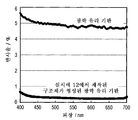
도 16은, 실시예 12에서 제조된 반사방지막의 반사율의 파장 의존성을 나타내는 그래프이다.
도 17의 17A 및 17B는, 각각, 실시예 20에서의 석영 유리 기판 상의 플라즈마 에칭에 의해 형성된 복수의 미세 원추체-형상의 돌출부로 구성된 구조체의 주사 전자 현미경 사진이다.
도 18의 18A 및 18B는, 각각, 실시예 27에서의 메소다공성 실리카 막 상에 에칭 장치를 구성하는 재료에 기인하는 컨테미네이션을 섬 형상으로 퇴적시키면서 플라즈마 에칭을 수행함으로써 형성된 복수의 미세 원추체-형상의 돌출부로 구성된 구조체의 주사 전자 현미경 사진이다.
도 19의 19A 및 19B는, 각각, 주기 및 크기가 서로 상이한 복수의 불규칙 형상을 갖는 발수성 막의 구성을 나타내는 모식도이다.
도 20의 20A 및 20B는, 각각, 실시예 31에서 제조된 발수성 막 상에서의 물의 접촉각을 측정하는 데 사용되는 사진이다.
도 21의 21A, 21B, 21C 및 21D는, 각각, 실시예 33에 기재된 주기 및 크기가 서로 상이한 복수의 불규칙 형상을 갖는 발수성 막을 제조하는 단계를 나타내는 모식도이다.
도 22는, 반사방지가 수행되는 부재의 굴절률 n4 (n기판)와 미세구조체의 굴절률 n3 (n막) 사이의 차와, 상기 부재와 구조체 사이의 계면에서의 반사율 사이의 관계를 나타내는 도이다.
도 23은 실시예 7의 제조 단계를 나타내는 도이다.
도 24는 표면 상에 보호층을 갖는 구조체의 모식도이다.
도 25의 25A, 25B 및 25C는, 각각, 표면 상에 보호층을 갖는 구조체의 모식도이다.
도 26의 26A, 26B 및 26C는, 각각, 원추체의 첨단이 부분적으로 결여된 형상을 나타내는 도이다.1A, 1B and 1C in Fig. 1 are schematic views showing the structure and the manufacturing procedure of the structure described in the first embodiment, respectively.
2A and 2B in Fig. 2 are schematic views of the structure described in the first embodiment, which are each composed of a meso structure having a structure in which cylindrical pores having a uniform diameter are regularly arranged.
3 is a schematic diagram of a structure composed of a plurality of meso structures having different structures in the first embodiment.
4A, 4B, 4C and 4D in Fig. 4 are schematic views showing the introduction state of the material into the mesopores, respectively.
5A, 5B, 5C, 5AS, 5BS and 5CS in Fig. 5 are schematic views showing the arrangement of a plurality of projections in the structure described in the first embodiment, respectively.
6A, 6B, 6AS and 6BS in Fig. 6 are schematic views showing a situation in which a plurality of projections are formed in the structure described in the first embodiment, respectively.
7A and 7B are schematic views showing the in-surface distribution of a plurality of projections in the structure described in the first embodiment, respectively.
8A, 8B, 8C, and 8D in FIG. 8 are graphs showing a schematic diagram showing the antireflection effect of the antireflection film described in the fourth embodiment and a change in the film refractive index associated with the filling of the material into the mesopores.
Fig. 9 is a schematic view showing a result of depth direction analysis of the amount of fluorine in the structure described in the first embodiment formed by performing plasma etching. Fig.
10 is a schematic diagram showing a method of forming a structure according to the fourth embodiment, which is manufactured by performing plasma etching while forming contaminants derived from a member constituting an etching apparatus in an island shape on a surface .
11 is a schematic diagram of a method for fabricating a semiconductor device according to a first embodiment of the present invention, which comprises forming a material having a small etch rate on a surface to increase the H / D ratio of a protrusion in the structure, Is a schematic view showing a method of forming a structure described in any one of the embodiments.
12 is a schematic view showing a step of manufacturing a structure corresponding to a negative of the structure described in any one of the first to third embodiments as a mold.
13A and 13B are scanning electron micrographs of a structure composed of a plurality of microcircular-shaped protrusions formed by plasma etching on the mesoporous silica film in Example 7, respectively.
14 is a schematic view showing the structure of a low-pressure CVD apparatus used in the step of filling an inorganic material in the mesopores.
15A and 15B are scanning electron micrographs of a structure composed of a plurality of microcircular-shaped protrusions formed by plasma etching on the mesoporous silica film in Example 12, respectively.
16 is a graph showing the wavelength dependency of the reflectance of the antireflection film produced in Example 12. Fig.
17A and 17B are scanning electron micrographs of a structure composed of a plurality of microcircular-shaped projections formed by plasma etching on a quartz glass substrate in Example 20, respectively.
18A and 18B in Fig. 18 are schematic diagrams showing a plurality of micro-conical-shaped microstructures formed by performing plasma etching on the mesoporous silica film in Example 27 while depositing contamination due to the material constituting the etching apparatus in an island shape, Shaped protrusions of the structure shown in FIG.
19A and 19B are schematic views showing the constitution of a water repellent film having a plurality of irregular shapes having different periods and sizes from each other.
20A and 20B in Fig. 20 are photographs used to measure the contact angle of water on the water repellent film produced in Example 31, respectively.
21A, 21B, 21C, and 21D in Fig. 21 are schematic views showing steps of manufacturing a water repellent film having a plurality of irregular shapes, which are different from each other in cycle and size, as described in Example 33. Fig.
22 is a diagram showing the relationship between the refractive index n4 (n substrate ) of the member on which reflection prevention is performed and the refractive index n3 (n film ) of the microstructure, and the reflectance at the interface between the member and the structure.
23 is a view showing a manufacturing step of the seventh embodiment.
24 is a schematic diagram of a structure having a protective layer on the surface.
25A, 25B and 25C in Fig. 25 are schematic views of a structure having a protective layer on the surface, respectively.
26A, 26B, and 26C in Fig. 26 each show a shape in which the tip of the conical body is partially missing.
실시양태의 설명Description of Embodiments
이하, 본 발명의 실시양태의 예를 이용하여 본 발명을 상세히 설명한다.Hereinafter, the present invention will be described in detail with reference to examples of embodiments of the present invention.
제1 실시양태In the first embodiment
먼저, 본 발명의 제1 실시양태를 설명한다.First, a first embodiment of the present invention will be described.
도 1의 1A 내지 1C는 각각 본 실시양태에 따른 구조체의 모식도이다. 도 1의 1A는 구조체의 입체도이고, 도 1의 1B는 도 1의 1A의 구조체를 단면 1B-1B로 절단하였을 때의 단면도이다.1A to 1C in Fig. 1 are schematic diagrams of structures according to the present embodiment, respectively. 1A is a three-dimensional view of the structure, and 1B in Fig. 1 is a sectional view when the structure of 1A in Fig. 1 is cut in
본 실시양태의 구조체 (11)는, 표면 상에 복수의 돌출부 (12)를 갖는 구조체이고, 여기서, 돌출부 (12)는 메소구조를 갖고, 메소구조는 메소세공 (13)을 갖는 구조이다.The
구조체 (11)는 메소세공 (13)을 갖는 (포함하는) 메소구조를 형성한다. 본원에서 사용되는 바와 같은 용어 "메소세공"은, 국제 순수 응용 화학 연합(International Union of Pure and Applied Chemistry)의 정의에 따른 2 nm 이상 및 50 nm 미만의 직경을 갖는 세공을 지칭한다. 세공의 직경은, 세공의 단면적이 최소가 되는 단면에서의 세공의 직경을 의미한다. 세공의 단면이 원형인 경우, 직경은 원의 직경을 지칭하고, 단면의 형상이 다각형인 경우, 직경은 다각형의 대각선의 길이의 최대값을 지칭한다. 단면 형상이 부정형인 경우에는, 단면 형상을 가로지르는 최대 직경이 세공 직경으로서 정의된다. 또한, 메소구조는, 메소세공이, 세공 벽을 형성하는 재료로 형성된 매트릭스 (이하, 때때로 벽부로서 기재됨) 중에 배치됨으로써 얻어지는 구조를 지칭한다. 하기에 기재되는 바와 같이, 메소세공의 내부는 공극 (중공)일 수 있거나, 또는 메소세공 내에 유기 재료 또는 무기 재료가 존재할 수 있다. 여기서 본 발명 및 본 명세서에서는, 메소세공이 중공인 경우의 구조체를 "메소다공성 재료"로서 지칭한다. 메소다공성 재료의 공극률은 바람직하게는 20% 이상 및 80% 이하이다. 물론, 30% 이상 내지 65% 이하의 공극률 범위는 20% 이상 내지 80% 이하의 메소다공성 재료의 공극률 범위 내에 포함됨을 인지하여야 한다.The
본 실시양태의 구조체 (11)는 도 1의 1A 내지 1C에 나타낸 바와 같은 복수의 돌출부 (12)를 갖는다. 돌출부 (12)는, 돌출부 (12)가 저부 (16)로부터 첨단 (17)을 향하는 방향 (18)에 대해 수직인 면 (19)으로 절단될 때 단면적이 방향 (18)을 따라 감소하는 형상 (다시 말해서, 저부 (16)로부터 첨단 (17)을 향하는 방향에 대하 수직인 단면적이 상기 방향을 따라 감소하는 형상)을 형성한다. 돌출부를 면 (19)으로 절단하여 얻어진 단면 중에 메소세공의 일부를 형성하는 중공 부분이 존재하는 경우에는, 중공 부분의 면적이 절단된 단면적 중에 포함됨을 인지하여야 한다. 돌출부 (12)는, 각각 바람직하게는, 그의 첨단부의 면적이 실질적으로 0이 되는 원추 형상 또는 원추체의 첨단이 부분적으로 결여된 형상인 원추부인 것이 바람직하지만, 면적이 반드시 방향 (18)을 따라 단조 감소할 필요는 없고, 돌출부는 돌출부가 원추 형상 또는 원추체에 근사할 수 있는 형상을 갖는 한 부분적으로 비틀린 형상을 가질 수 있다. 저부 (16)로부터 첨단 (17)을 향하는 방향 (18)에 대해 수직인 단면적이 상기 방향을 향하는 방향을 따라 변하지 않는 (동일한) 영역이 부분적으로 존재할 수 있음을 인지하여야 한다. 또한, 돌출부는, 그의 첨단이 분할된 (첨단이 복수의 부분으로 분할된) 형상을 가질 수 있다. 하기 기재에서, "원추부"라는 표현은, 첨단부의 면적이 실질적으로 0이 되는 원추 형상 또는 원추체의 첨단이 부분적으로 결여된 형상 둘 다를 포함하는 것으로 정의됨을 인지하여야 한다. 본원에서 정의되는 바와 같은 "원추체의 첨단이 부분적으로 결여된 형상"이라는 표현은 하기 형상으로서 정의된다: 도 26의 26A에 나타낸 원추면 (2301)을 연장시킬 때 형성되는 가상 원추체 A (2302) (도 26의 26B에 나타냄)의 높이 (2303)를 1로 정의할 때, 도 26의 26C에 나타낸 바와 같이 결여된 부분의 가상 원추체 A의 정점으로부터 가장 멀리있는 점 (2304)을 저면에 포함하며 가상 원추체 A의 정점과 동일한 정점 (2307)을 갖는 가상 원추체 B (2305)의 높이 (2306)가 1/7 이하임. 돌출부가 이러한 형상을 갖는 경우, 구조체 (11)의 겉보기 굴절률 실수부(real part)가 방향 (18)을 따라 감소한다.The
구조체 (11)의 돌출부 (12)의 저변의 길이를 D로 나타내고, 돌출부 (12)의 높이를 H로 나타낼 때, H/D 비율 (이하, 때때로 종횡비로서 기재됨)은 바람직하게는 1/2 이상, 더욱 바람직하게는 1.0 이상, 훨씬 더 바람직하게는 3.0 이상, 가장 바람직하게는 5.0 이상이다. 돌출부 (12)가 원추부인 경우, 1/2 이상의 H/D 비율은, 구조체를 사용한 반사방지막의 형성시 전자기파의 반사를 효과적으로 억제할 수 있다. 돌출부 (12)가 원추부가 아닌 경우에는, 1.0 이상의 H/D 비율이 반사를 효과적으로 억제할 수 있다. 1/2 이상의 H/D 비율은, 도 1의 1B에 나타낸 본 실시양태의 구조체의 단면 투영도에서 각각의 돌출부의 정점각 θ이 예각이라는 것을 의미함을 인지하여야 한다. H/D 비율이 증가함에 따라, 많은 경우에 보다 우수한 반사방지 특성이 얻어진다. 그러나, H/D 비율이 과도하게 큰 경우에는, 구조체의 기계적 강도가 감소할 수 있다. 따라서, H/D 비율은 강도의 관점에서 바람직하게는 12 이하이다.When the height of the protruding
여기서, 저변 D는, 저부 (16)의 형상을 갖는 저면의 중력 중심 위치를 통과하여 그의 외주 상의 두 점을 연결하는 선분의 최소 거리를 나타낸다. 또한, 저부는 각각의 돌출부의 말단을 일주함으로써 형성된 형상을 나타내고, 다시 말해서, 이는 돌출부 사이의 경계선으로 둘러싸인 형상이다.Here, the bottom D represents the minimum distance of a line segment passing through the gravity center position of the bottom surface having the shape of the
또한, 돌출부 (12)의 높이 H는 돌출부 (12)의 첨단 (17)과 저부 (16)의 중심을 연결하는 선분의 길이를 나타낸다. 첨단 (17)과 저부 (16)의 중심을 연결하는 선분의 단부가 저부 (16) 내에 존재하지 않는 경우, 높이 H는 돌출부 (12)의 첨단 (17)으로부터 저부 (16)를 포함하는 평탄 표면으로 수직으로 내린 선분의 길이로서 정의됨을 인지하여야 한다.The height H of the
돌출부의 첨단이 분할된 형상을 형성하는 경우, 돌출부의 단면 SEM 화상에서, 각각의 정점으로부터, 정점을 포함하는 돌출부와 그에 인접하는 또 다른 돌출부의 교차점까지의 원추면을, 돌출부의 단면 SEM 화상에서 복수의 교차점의 기판에 가장 가까운 교차점의 높이까지 연장시킴으로써 형성된 복수의 가상 원추체를 설정함으로써, 저부의 저변 D 및 높이 H를 계산한다.In the cross-sectional SEM image of the protrusion, when the tip of the protrusion forms the divided shape, the conical surface from each apex to the point of intersection of the protrusion including the vertex and another protrusion adjacent thereto is formed as a plurality To the height of the intersection closest to the substrate at the intersection of the intersection points of the virtual concavities, thereby calculating the bottom D and height H of the bottom portion.
돌출부 (12)의 높이 H는 바람직하게는 50 nm 이상, 더욱 바람직하게는 100 nm 이상, 가장 바람직하게는 200 nm 이상이다.The height H of the projecting
돌출부 (12)의 첨단 (17) 사이의 평균 간격 (도 1의 1B에서 p) (평균 첨단-대-첨단 간격)은 바람직하게는 400 nm 이하이다. 돌출부 (12)의 첨단 사이의 평균 간격이 상기 값 초과가 되는 경우, 광 산란이 현저해지고, 이는 광학 용도의 경우 성능 저하를 일으킬 수 있다.The average spacing (p in FIG. 1B) between the
돌출부 (12)의 형상에 대해서는, 첨단 (17) 사이의 평균 간격이 400 nm 이하이고, 높이 H (도 1의 1B에서 H)가 50 nm 이상이고, H/D 비율이 1.0 이상인 것이 바람직하다. 첨단 (17) 사이의 평균 간격이 100 nm 이하이고, 높이 H가 50 nm 이상이고, H/D 비율이 3.0 이상인 것이 더욱 바람직하다. 첨단 (17) 사이의 평균 간격이 100 nm 이하이고, 높이 H가 300 nm 이상이고, H/D 비율이 3.0 이상인 것이 훨씬 더 바람직하다.As for the shape of the protruding
본 실시양태의 구조체에서 돌출부의 배열로서는 임의의 배열이 이용될 수 있다. 그의 예는, 도 5의 5A (도 5의 5AS는 도 5의 5A의 5AS-5AS 단면임)에 나타낸 바와 같은 육방 밀집 배열, 입방 밀집 배열 (도 5의 5B) (도 5의 5BS는 도 5의 5B의 5BS-5BS 단면임), 및 랜덤 배열 (도 5의 5C) (도 5의 5CS는 도 5의 5C의 5CS-5CS 단면임)을 포함한다. 도 5의 5A 내지 5C에서, 원은 각각의 돌출부의 저부의 윤곽을 나타내고, 원의 중심의 흑색 점은 돌출부의 정점을 모식적으로 나타낸다. 돌출부의 저면이 완전히 원형일 필요는 없다. 돌출부의 저면은 타원일 수 있다. 상기 돌출부의 정점이 그의 저부의 윤곽 중심에 있을 필요는 없다. 도 5의 5A 내지 5C 및 5AS 내지 5CS에 모식적으로 나타낸 돌출부의 배열에서, 각각의 돌출부는 그의 단면의 모식도로부터 알 수 있는 바와 같이 독립적으로 형성되어 있다.Any arrangement may be used as the arrangement of the protrusions in the structure of this embodiment. 5B) in FIG. 5 (5BS in FIG. 5 corresponds to a cross-sectional view of FIG. 5A), as shown in FIG. 5A (5AS in FIG. 5 is 5AS- 5BS of FIG. 5), and a random arrangement (5C of FIG. 5) (5CS of FIG. 5 is 5CS-5CS cross section of FIG. 5C). 5A to 5C, the circle represents the outline of the bottom of each protrusion, and the black dot at the center of the circle schematically represents the apex of the protrusion. The bottom surface of the protrusion need not be completely circular. The bottom surface of the protrusion may be an ellipse. It is not necessary that the apex of the protrusion be at the center of the contour of its bottom. In the arrangement of projections shown schematically in Figs. 5A to 5C and 5AS to 5CS, each projecting portion is formed independently as seen from the schematic view of its cross section.
그러나, 도 6의 6A에 나타낸 바와 같이, 본 실시양태의 구조체의 돌출부는, 인접한 돌출부의 능선 (또는 원추면)의 일부가 기판 표면 상부 부분에서 서로 교차할 수 있도록 배열될 수 있다 (도 6의 6AS는 6A의 6AS-6AS 단면임). 또한, 돌출부의 저부 또는 능선이 반드시 서로 접촉하거나 교차하여야 하는 것은 아니고, 도 6의 6B (도 6의 6BS는 6B의 6BS-6BS 단면임)에 나타낸 바와 같이 돌출부 및 또 다른 돌출부가 서로 접촉하지 않을 수도 있다. 그러나, 본 실시양태의 구조체가 하기에 기재되는 반사방지막과 같은 용도에 사용되는 경우에는, 돌출부와 또 다른 돌출부 사이의 간격 증가가 구조체의 전체 표면에 대한 평탄 표면을 갖는 부분의 비율을 증가시킨다. 그 결과, 계면에서의 굴절률 변화가 급격해지고, 하기 문제가 발생할 수 있다: 반사방지 특성이 감소함. 인접한 돌출부의 능선이 기판 표면 상부 부분에서 서로 교차하는 도 6의 6A에 나타낸 바와 같은 구성이 이러한 용도에서 바람직하다.6A, the protrusions of the structure of this embodiment can be arranged such that a part of the ridgeline (or conical surface) of the adjacent protrusions can intersect with each other at the upper portion of the substrate surface (see 6AS of Fig. 6 Is the 6AS-6AS section of 6A). Also, the bottoms or ridges of the protrusions do not necessarily have to contact or cross each other, and as shown in Fig. 6B (6BS in Fig. 6 is 6BS-6BS cross section of 6B), the protrusions and other protrusions It is possible. However, when the structure of this embodiment is used in applications such as the anti-reflective coating described below, an increase in the spacing between the protrusions and another protrusion increases the proportion of the portion having a flat surface with respect to the entire surface of the structure. As a result, the refractive index change at the interface becomes abrupt, and the following problems may arise: the antireflection characteristic is reduced. 6A in which the ridges of the adjacent protrusions cross each other at an upper portion of the substrate surface are preferable in this use.
본 실시양태의 구조체에서 돌출부는 구조체의 전체에 걸쳐 균일하게 형성되는 것이 바람직하다. 본원에서 기재되는 바와 같은 용어 "균일한"은, 도 7의 7A와 같이 돌출부가 실질적으로 일정한 밀도로 분포된 상태를 지칭하며, 도 7의 7B와 달리 돌출부가 존재하지 않는 영역이 구조체의 일부에 형성되지 않은 상태를 지칭한다. 도 7의 7A 및 7B에서, 원은 각각의 돌출부의 저부의 윤곽을 나타내고, 원의 중심의 흑색 점은 돌출부의 정점을 모식적으로 나타낸다. 구체적인 균일성은 하기에 기재되는 바와 같다. 돌출부의 첨단 사이의 평균 간격을 p로 나타내고, 첨단 사이의 간격의 분포의 표준 편차를 σ로 나타낼 때, 하기 식 1이 만족된다.In the structure of this embodiment, it is preferable that the protrusions are formed uniformly throughout the structure. The term "uniform" as described herein refers to a state in which protrusions are distributed at a substantially constant density as in 7A of Fig. 7, and unlike 7B in Fig. 7, Formed state. 7A and 7B, the circles represent the contours of the bottoms of the respective protrusions, and the black points at the center of the circle represent the apexes of the protrusions. Specific uniformity is as described below. When the average distance between the tips of the projections is represented by p and the standard deviation of the distribution of the intervals between the tips is represented by?, The following
<식 1><
0.1<σ/p<0.50.1 <? / P <0.5
상기 조건은, 평균 간격 p의 값에 대하여 각각의 돌출부 사이의 간격의 변동 정도가 포함되는 범위를 의미한다. 상기 값이 0.1 미만인 경우에는, 돌출부가 일정한 간격으로 배열되어, 바람직하지 않은 간섭 효과를 일으킬 수 있다. 또한, 상기 값이 0.5 초과인 경우에는, 돌출부의 형성 위치의 폭넓은 분포가 광학 특성의 불균일성으로 나타날 수 있다.The above condition means a range including a degree of fluctuation of the interval between the respective protrusions with respect to the value of the average interval p. When the value is less than 0.1, the protrusions are arranged at regular intervals, which may cause an undesirable interference effect. Further, when the value is more than 0.5, the wide distribution of the formation positions of the protrusions may appear as nonuniformity of optical characteristics.
첨단 간격의 계산은 하기 방법에 기초한 것임을 인지하여야 한다: 미세구조체를 구조체 바로 위로부터 촬영하여 얻은 전자 현미경 사진의 화상 처리를 통해 각각의 첨단부의 좌표를 취득하고, 이어서 델로네(Delaunay) 삼각분할법 (각각의 주어진 첨단부의 좌표를 정점으로서 사용하여 삼각형을 형성하고, 그 삼각형의 외접원이 정점 이외의 임의의 점을 포함하지 않는 조건 하에 분할을 수행하는 것을 포함하는 방법)에 의해 각각의 돌출부의 첨단 사이의 거리를 얻는다. 미세구조체가 형성된 영역 내에서 각각 1 ㎛의 시야를 갖는 전자 현미경 사진을 치우침없이 20개소에서 얻고, 이어서 각각의 첨단 사이의 거리를 계산함으로써 평균 간격 p 및 표준 편차 σ를 결정한다.It should be noted that the calculation of the leading edge interval is based on the following method: the coordinates of each leading edge are obtained through image processing of the electron micrograph obtained by photographing the microstructure right above the structure, and then the Delaunay triangulation method A method comprising forming a triangle using the coordinates of each given tip as a vertex and performing splitting under conditions that the circumscribed circle of the triangle does not include any point other than the vertex) . An electron micrograph having a field of view of 1 mu m in the region where the microstructure is formed is obtained at 20 locations without bias and then the distance between each peak is calculated to determine the mean spacing p and the standard deviation sigma.
본 실시양태의 구조체에서 메소세공은 바람직하게는 실린더형 형상을 갖고, 바람직하게는 균일한 직경을 갖는다. 메소세공이 실린더형 형상을 갖고 균일한 직경을 갖는 것이 더욱 바람직하다. 이러한 경우, 하기에 기재되는 중공 메소세공 내에 재료를 충전시키는 것을 포함하는 방법이 용이하고, 메소세공 내로 충전되는 재료의 양이 용이하게 조정된다. 여기서, 본 발명 및 본 명세서에서 사용되는 바와 같은 어구 "균일한 직경을 갖는"은 하기와 같이 정의된다: 전자 현미경으로 관찰된 메소세공의 직경이 메소세공의 직경의 평균에 대하여 ±50%의 범위의 크기 내에 포함됨.In the structure of the present embodiment, the mesopores preferably have a cylindrical shape, and preferably have a uniform diameter. More preferably, the mesopores have a cylindrical shape and a uniform diameter. In such a case, a method including filling the material in the hollow mesopores described below is easy, and the amount of material filled into the mesopores is easily adjusted. Here, the phrase "having a uniform diameter" as used herein and in the present description is defined as follows: the diameter of the mesopores observed with an electron microscope is within a range of +/- 50% ≪ / RTI >
그러나, 메소세공의 형상이 실린더형이 아니면 반드시 본 발명의 효과가 얻어지지 않는다는 것은 아니다. 구 형상, 타원 구 형상, 및 로드 형상 등의 다양한 형상의 메소세공 또한 실용가능하다. 도 2의 2A 및 2B에 모식적으로 나타낸 바와 같이, 메소세공이 실린더형 형상을 갖는 경우, 많은 경우에 실린더형 메소세공 (21)은 기판에 평행하게 배향된다. 도 2의 2A는 실린더형 메소세공을 메소세공의 길이 방향에서 본 모식도이고, 도 2의 2B는 메소세공을 길이 방향에 수직인 방향에서 본 모식도이지만, 실린더형 메소세공의 방향은 구조체 내에서 제어되지 않을 수 있다. 굴절률의 균일성 관점에서, 균일한 직경을 갖는 실린더형 메소세공이 구조체 내에서 주기적으로 배열되는 것이 바람직하다. 메소세공 (세공)이 구조체 내에서 주기적으로 배열된 예로서는, 메소세공이, 도 2의 2A에 나타낸 바와 같이 메소세공이 육각형으로 나타내어지는 배열을 형성하는 육방 밀집과 같이 규칙적으로 배열된 경우가 주어진다. 메소세공의 배열은 육방 밀집으로 제한되지 않고, 세공이 직사각형 또는 정사각형을 형성하는 배열 또한 실용가능하다.However, unless the shape of the mesopores is cylindrical, it does not necessarily mean that the effect of the present invention can not be obtained. Mesopores of various shapes such as a spherical shape, an elliptical spherical shape, and a rod shape are also practically usable. As schematically shown in FIGS. 2A and 2B in FIG. 2, when the mesopores have a cylindrical shape, in many cases, the cylindrical meso-
규칙적 배열은 바람직하게는, 메소구조를 갖는 본 발명의 구조체를 X선 회절 분석으로 분석할 때 1.0 nm 이상의 주기 구조에 상응하는 회절 피크가 관찰되는 배열이고, 더욱 바람직하게는 5.0 nm 이상의 주기 구조에 상응하는 회절 피크가 관찰되는 배열이다. 1.0 nm 이상의 주기 구조에 상응하는 회절 피크가 관찰되는 배열은, 도 2의 2A 및 2B에 나타낸 바와 같은 세공의 규칙적 배열에 의해 규정되는 구조 주기 d가 1.0 nm 이상이라는 것을 의미함을 인지하여야 한다. 메소세공이 실린더형 형상을 갖지 않는 경우에도, 메소세공이 규칙적으로 배열되는 것이 바람직하고, 배열이 바람직하게는 X선 회절 분석에서 5.0 nm 이상의 주기 구조에 상응하는 회절 피크가 관찰되는 배열이다. 그러나, 메소세공이 규칙적으로 배열되지 않으면 반드시 본 발명의 효과가 얻어지지 않는다는 것은 아니고, 본 실시양태의 구조체의 메소세공은, 예를 들어, 실린더형 메소세공이 불규칙적으로 연결된 구조를 가질 수 있다.The regular arrangement is preferably an arrangement in which a diffraction peak corresponding to a periodic structure of 1.0 nm or more is observed when the structure of the present invention having a meso structure is analyzed by X-ray diffraction analysis, more preferably a periodic structure of 5.0 nm or more And the corresponding diffraction peak is observed. It should be noted that the arrangement in which the diffraction peaks corresponding to the periodic structure of 1.0 nm or more are observed means that the structural period d defined by the regular arrangement of the pores as shown in 2A and 2B in Fig. 2 is 1.0 nm or more. Even when the mesopores do not have a cylindrical shape, it is preferable that the mesopores are arranged regularly, and the arrangement is preferably such that an X-ray diffraction analysis shows that a diffraction peak corresponding to a periodic structure of 5.0 nm or more is observed. However, if the mesopores are not regularly arranged, the effect of the present invention is not necessarily obtained, and the mesopores of the structure of the present embodiment may have a structure in which, for example, cylindrical mesopores are irregularly connected.
본 실시양태의 메소구조를 갖는 구조체가, 도 3에 나타낸 바와 같이 상이한 구조를 갖는 복수의 메소구조 (31), (32)로 구성된 경우, 하기에 기재되는 바와 같이, 하나의 돌출부에서, 돌출부의 저부 근처의 메소세공 및 그의 첨단부 근처의 메소세공 내에 존재하는 유기 화합물 또는 무기 화합물의 존재량을 변화시킴으로써 구조체에 굴절률의 변화를 제공할 수 있다. 본원에서 기재되는 바와 같은 용어 "상이한 구조"는, 메소세공 직경, 메소세공의 배열, 및 메소세공 사이의 간격 등의 구조 파라미터 중 어느 하나가 상이함을 의미한다. 도 3은 돌출부의 첨단 근처의 메소세공의 직경이 돌출부의 저부에서의 메소세공의 직경보다 큰 경우를 모식적으로 나타내지만, 본 발명에서 상이한 구조를 갖는 복수의 메소구조는 메소세공 직경이 서로 상이한 구조체로 제한되지 않는다.When the structure having the meso structure of this embodiment is composed of a plurality of
본 실시양태의 구조체의 벽부 (메소세공을 형성하는 매트릭스)를 구성하는 물질로서는, 금속, 질화물, 탄화물, 플루오린화물, 붕화물, 산화물 등을 성분으로서 함유하는 물질이 사용될 수 있다. 본 발명의 구조체가 반사방지막 등의 광학 재료에 사용되는 경우, 벽부를 구성하는 물질은 바람직하게는 가시광에 대해 투명하고 큰 밴드 갭을 갖는 물질이고, 2.5 eV 이상 내지 10 eV 이하 범위의 밴드 갭을 갖는 물질이 바람직하게 사용된다. 그의 예는, 산화규소, 산화티타늄, 산화주석, 산화지르코늄, 산화니오븀, 산화탄탈럼, 산화알루미늄, 산화텅스텐, 산화하프늄, 및 산화아연을 포함한다. 이들 중, 재료의 안정성을 고려하면, 산화규소, 산화지르코늄 및 산화티타늄이 특히 바람직하게 사용된다. 또한, 벽부를 구성하는 재료가 산화티타늄인 경우에는, 산화티타늄의 적어도 일부가 결정화되는 것이 바람직하다. 이는 하기 이유 때문이다. 산화티타늄의 적어도 일부가 결정화되면, 벽부의 재료의 굴절률이 산화티타늄이 결정화되지 않은 경우에 비해 추가로 증가할 수 있다. 또한, 산화티타늄의 광 반도체로서의 특성이 현저하게 발휘된다. 산화티타늄의 결정화도는, 예를 들어, X선 회절 분석에 의해 측정될 수 있음을 인지하여야 한다.As the material constituting the wall portion (matrix for forming mesopores) of the structure of the present embodiment, a material containing a metal, a nitride, a carbide, a fluoride, a boride, an oxide and the like as a component can be used. When the structure of the present invention is used in an optical material such as an antireflection film, the material constituting the wall portion is preferably a material which is transparent to visible light and has a large band gap, and has a band gap in the range of 2.5 eV to 10 eV Is preferably used. Examples thereof include silicon oxide, titanium oxide, tin oxide, zirconium oxide, niobium oxide, tantalum oxide, aluminum oxide, tungsten oxide, hafnium oxide, and zinc oxide. Of these, silicon oxide, zirconium oxide and titanium oxide are particularly preferably used in consideration of the stability of the material. Further, when the material constituting the wall portion is titanium oxide, it is preferable that at least a part of the titanium oxide is crystallized. This is because of the following reasons. If at least a portion of the titanium oxide is crystallized, the refractive index of the material of the wall portion may further increase as compared to the case where the titanium oxide is not crystallized. Further, the characteristics of titanium oxide as an optical semiconductor are remarkably exhibited. It should be appreciated that the crystallinity of the titanium oxide can be measured, for example, by X-ray diffraction analysis.
본 실시양태의 구조체에서의 메소세공 (13)에 대하여, 메소세공의 내부는 공극 (중공)일 수 있거나, 또는 메소세공 내에 유기 재료 또는 무기 재료가 존재할 수 있다. 여기서, 물론, 어구 "메소세공 내에 유기 재료 또는 무기 재료가 존재함"은, 메소세공 내에 단지 유기 재료만이 존재하는 경우, 단지 무기 재료만이 존재하는 경우, 유기-무기 하이브리드 재료와 같이 유기 재료 및 무기 재료가 존재하는 경우, 및 유기 재료 및/또는 무기 재료 및 임의의 다른 재료가 존재하는 경우를 포함한다. 또한, 메소세공 내에 유기 재료 또는 무기 재료가 존재하는 경우, 유기 재료 또는 무기 재료는 단지 메소세공의 적어도 일부에 존재하여야 하고, 이러한 상황은, 유기 재료 또는 무기 재료가 복수의 메소세공의 일부에 완전히 충전된 상태로 존재하는 경우 및 복수의 메소세공의 대부분이 각각 그의 내부의 일부에 존재하는 유기 재료 또는 무기 재료를 갖는 메소세공인 경우를 포함한다. 본 발명에서는, 심지어 복수의 메소세공 전부가 유기 재료 또는 무기 재료로 완전히 충전된 경우도, 메소구조가 메소세공을 갖고, 여기에 유기 재료 또는 무기 재료가 존재하기 때문에, "메소구조가 메소세공을 갖는다"는 개념에 포함됨을 인지하여야 한다.For the
메소세공 내에 존재하는 유기 재료의 예는, 하기에 기재되는 메소구조체 제조시 구조-규정제로서 사용되는 양친매성 물질, 중합체 등의 고분자량 재료, 및 10,000 미만의 분자량을 갖는 단량체 재료를 포함한다.Examples of organic materials present in the mesopores include amphipathic materials used as structure-regulating agents in the preparation of the meso structure described below, high molecular weight materials such as polymers, and monomer materials having a molecular weight of less than 10,000.
또한, 메소세공 내에 유기 재료가 존재하는 예로서는, 유기 재료가 소수성 관능기를 갖고, 메소세공의 표면이 소수성 관능기로 화학적으로 개질된 예가 주어진다. 이러한 경우, 하기에 기재되는 바와 같이, 형성되는 복수의 돌출부를 갖는 구조체의 형태가 제어될 수 있다. 여기서 본 발명 및 본 명세서에서 소수성 관능기는 하기 관능기로서 정의된다: 세정된 용융 석영 기판 표면을 그 화합물로 포화 수준까지 개질한 경우, 개질 후 표면에서의 물의 접촉각이 90° 초과임. 이러한 소수성 관능기의 예는 알킬 기 및 플루오로알킬 기를 포함한다.An example of the presence of an organic material in the mesopores is an example in which the organic material has a hydrophobic functional group and the surface of the mesopores is chemically modified with a hydrophobic functional group. In such a case, as described below, the shape of the structure having a plurality of protrusions to be formed can be controlled. Herein, the hydrophobic functional groups in the present invention and herein are defined as the following functional groups: when the cleaned fused quartz substrate surface is modified to the saturation level with the compound, the contact angle of water on the surface after modification is greater than 90 °. Examples of such hydrophobic functional groups include alkyl groups and fluoroalkyl groups.
메소세공 내에 존재하는 무기 재료의 예는, 전도성 재료, 절연성 재료, 및 반도체 재료 등의 폭넓게 다양한 재료로부터 선택될 수 있다.Examples of the inorganic material present in the mesopores can be selected from a wide variety of materials such as a conductive material, an insulating material, and a semiconductor material.
예를 들어, 무기 재료로서는, 금속, 질화물, 탄화물, 플루오린화물, 붕화물, 또는 산화물을 주성분으로서 사용하는 무기 재료가 사용될 수 있다. 무기 재료는 단일 조성을 가질 수 있거나, 2종 이상의 혼합물일 수 있거나, 또는 복합 재료일 수 있다. 본 실시양태의 구조체가 반사방지막 등의 광학 재료에 사용되는 경우, 메소세공 내에 존재하는 무기 재료는 바람직하게는 큰 밴드 갭을 갖고 가시광에 대해 투명한 재료이고, 2.5 eV 이상 내지 10 eV 이하 범위의 밴드 갭을 갖는 재료가 특히 바람직하게 사용된다. 그의 예는, 산화규소, 산화티타늄, 산화주석, 산화지르코늄, 산화니오븀, 산화탄탈럼, 산화알루미늄, 산화텅스텐, 산화하프늄, 및 산화아연을 포함한다. 이들 중, 재료의 높은 투명성을 고려할 때, 산화규소, 산화지르코늄 및 산화티타늄이 광학 용도와 관련하여 특히 바람직하게 사용된다.For example, as the inorganic material, an inorganic material using a metal, a nitride, a carbide, a fluoride, a boride, or an oxide as a main component may be used. The inorganic material may have a single composition, may be a mixture of two or more, or may be a composite material. When the structure of this embodiment is used for an optical material such as an antireflection film, the inorganic material present in the mesopores is preferably a material having a large band gap and transparent to visible light, and a band in the range of 2.5 eV or more to 10 eV or less A material having a gap is particularly preferably used. Examples thereof include silicon oxide, titanium oxide, tin oxide, zirconium oxide, niobium oxide, tantalum oxide, aluminum oxide, tungsten oxide, hafnium oxide, and zinc oxide. Of these, silicon oxide, zirconium oxide and titanium oxide are particularly preferably used in connection with optical applications, in view of the high transparency of the material.
메소세공 내에 존재하는 무기 재료는, 돌출부를 갖는 구조체의 메소세공 내에, 도 4의 4A 및 4B에 모식적으로 나타낸 바와 같이 균일하게 분포되도록 포함될 수 있거나, 또는 메소세공 내의 무기 재료의 충전율이 돌출부의 저부로부터 그의 첨단을 향하는 방향으로 감소할 수 있도록, 바람직하게는 공극률이 돌출부의 저부로부터 그의 첨단을 향하는 방향으로 증가할 수 있도록 무기 재료의 충전량이 제어될 수 있다. 이러한 충전율의 국소적 변화는, 예를 들어, 상기에 기재된 바와 같이, 돌출부를 형성하는 메소구조체를, 상이한 구조를 갖는 복수의 메소구조체로 구성함으로써 달성될 수 있다 (도 4의 4D).The inorganic material present in the mesopores may be included in the mesopores of the structure having the protrusions so as to be uniformly distributed as shown schematically in Figs. 4A and 4B in Fig. 4, or the filling rate of the inorganic material in the mesopores may be The filling amount of the inorganic material can be controlled so that the porosity can be increased in the direction from the bottom of the projection toward the tip thereof so as to decrease in the direction toward the tip of the tip from the bottom. This local variation of the filling rate can be achieved, for example, by constructing the meso structure forming the protrusion, as described above, with a plurality of meso structures having different structures (4D in Fig. 4).
메소세공 내의 무기 재료의 충전율이 돌출부의 저부로부터 그의 첨단을 향하는 방향으로 감소하는 구조체의 경우, 메소구조를 갖는 구조체를 형성하는 재료를 구성하는 원소에 대한 무기 재료를 구성하는 원소의 국소적 존재비를 나타내는 비율 "(무기 재료를 구성하는 원소의 양)/(메소구조를 갖는 구조체를 구성하는 원소의 양)"이 돌출부의 저부로부터 그의 첨단을 향하는 방향으로 감소한다 (도 4의 4C).In the case of a structure in which the filling rate of the inorganic material in the mesopores decreases from the bottom of the projection toward the tip thereof, the local abundance ratio of the elements constituting the inorganic material to the elements constituting the material forming the structure having the meso structure Quot; (amount of elements constituting the inorganic material) / (amount of elements constituting the structure having the meso structure) "decreases in the direction from the bottom of the projection toward the tip thereof (FIG. 4C).
비율 "(무기 재료를 구성하는 원소의 양)/(메소구조를 갖는 구조체를 구성하는 원소의 양)"은, 이온 스퍼터링을 반복하면서 광전자 분광법의 깊이방향 분석을 수행함으로써 구할 수 있다.The ratio "(the amount of the element constituting the inorganic material) / (the amount of the element constituting the structure having the meso structure)" can be obtained by performing the depth direction analysis of the photoelectron spectroscopy while repeating ion sputtering.
메소세공 전부가 충전되는 경우, 벽부를 구성하는 재료는 바람직하게는 메소세공 내에 존재하는 재료와 상이함을 인지하여야 한다.When all of the mesopores are filled, it is to be recognized that the material constituting the wall portion preferably differs from the material present in the mesopores.
많은 경우에 본 실시양태의 구조체는 기판 상에 형성된다. 본 발명의 구조체가 위에 형성될 수 있는 한, 기판의 재료 및 형상은 기본적으로 제한되지 않는다.In many cases, the structure of this embodiment is formed on a substrate. The material and the shape of the substrate are basically not limited as long as the structure of the present invention can be formed thereon.
또한, 본 실시양태의 구조체는 그의 표면 상에 보호층을 가질 수 있다.In addition, the structure of this embodiment may have a protective layer on its surface.
이하, 보호층을 상세히 설명한다.Hereinafter, the protective layer will be described in detail.
도 24는 표면 상에 존재하는 돌출부로 형성된 구조체의 모식도를 나타낸다. 기판 (2201) 상에 형성된 돌출부 (2202)가 각각 그의 표면 상에 보호층 (2203)을 갖는 경우, 돌출부 (2202)의 메소세공 (2204)이 수분을 함유하는 공기로부터 차폐된다. 그 결과, 돌출부 (2202)를 형성하는 메소구조 내부로의 수분의 흡착이 억제될 수 있고, 따라서 안정한 굴절률이 유지될 수 있다. 또한, 메소세공 (2204)을 통한 기판 (2201)으로의 수분의 도달이 유사하게 억제된다. 따라서, 알칼리 금속 산화물, 알칼리 토금속 산화물, 또는 산화붕소 등의 산화물 성분을 함유하는 기판이 사용되는 경우에도, 이러한 성분의 용출과 관련된 흐림 또는 백화의 발생이 방지될 수 있다. 본원에서 기재되는 바와 같은 용어 "세공"은, 세공 내부의 적어도 일부에 유기 재료 또는 무기 재료가 충전된 경우 이러한 재료로 완전히 충전되지 않은 부분에 생성된 세공을 포함함을 인지하여야 한다. 유사하게, 하기 기재에서 용어 "공극률"은, 세공 내부의 적어도 일부에 유기 재료 또는 무기 재료가 존재하는 경우, 유기 재료 또는 무기 재료가 충전된 상태에서 전체 부피에 대한 세공의 비율을 지칭한다.24 shows a schematic view of a structure formed of protrusions present on the surface. When the
돌출부 내로의 수분의 침투를 억제하기 위해, 보호층을 형성하는 재료로서는, 세공을 갖는 돌출부의 공극률보다 작은 공극률을 갖는 재료가 바람직하게 선택된다. 공극률의 크기는, 예를 들어, 보호층의 존재 또는 부재 하에서의 질소 기체 흡착법에 의해 얻어지는 흡착 및 탈착 등온선을 이용하여 평가할 수 있다. 본원에서 기재되는 바와 같은 용어 "흡착 및 탈착 등온선"은 IUPAC에 의해 정의된 카테고리의 등온선을 지칭하고, 등온선은 "Pure Appl. Chem., Vol. 57, p. 603 (1985)"에 기재되어 있다. 구체적으로, 단지 보호층을 갖지 않는 돌출부의 경우, 또는 돌출부의 공극률보다 큰 공극률을 갖는 보호층이 표면 상에 형성된 경우에는, 돌출부 내의 세공에 대한 흡착 및 탈착이 지배적이 되고, 따라서 등온선이 IV형 흡착-탈착 거동을 나타낸다. 한편, 돌출부의 공극률보다 작은 공극률을 갖는 보호층이 표면 상에 형성된 경우에는, 돌출부 내의 세공과 관련된 흡착-탈착 거동이 보호층에 의해 억제된다. 그 결과, 보호층의 표면에 대한 흡착-탈착 거동이 지배적이 되고, 따라서 흡착-탈착 거동이 II형 거동 또는 II형 거동에 가까운 거동을 나타낸다.As a material for forming the protective layer, a material having a porosity lower than that of the protrusions having pores is preferably selected so as to suppress the penetration of moisture into the protrusions. The size of the porosity can be evaluated using, for example, adsorption and desorption isotherms obtained by nitrogen gas adsorption methods in the presence or absence of a protective layer. The term "adsorption and desorption isotherms" as described herein refers to isotherms of the category defined by the IUPAC and isotherms are described in " Pure Appl. Chem., Vol. 57, p. 603 (1985) " . Specifically, in the case of protrusions having only a protective layer, or when a protective layer having a porosity larger than that of the protrusions is formed on the surface, adsorption and desorption to the pores in the protrusions become dominant, Adsorption-desorption behavior. On the other hand, when a protective layer having a porosity smaller than the porosity of the protrusions is formed on the surface, the adsorption-desorption behavior associated with the pores in the protrusions is suppressed by the protective layer. As a result, the adsorption-desorption behavior on the surface of the protective layer becomes dominant, and thus the adsorption-desorption behavior exhibits a behavior close to the II-type behavior or the II-type behavior.
보호층은 바람직하게는 메소세공을 갖는 돌출부의 표면의 전체 영역을 피복하지만, 제조 편의를 위해 보호층이 형성되지 않은 영역이 부분적으로 존재할 수 있다. 이러한 경우에도 보호층의 효과가 기대될 수 있지만, 보호층은 바람직하게는 메소세공을 갖는 돌출부의 표면의 50% 이상에 형성된다.The protective layer preferably covers the entire area of the surface of the protrusions having mesopores, but for the sake of ease of manufacture, there may be some areas where no protective layer is formed. Even in this case, the effect of the protective layer can be expected, but the protective layer is preferably formed on at least 50% of the surface of the protrusions having mesopores.
이하, 메소세공을 갖는 돌출부 및 그의 표면 상에 형성된 보호층을 도 25의 25A 내지 25C를 참조로 하여 더욱 상세히 설명한다. 여기서는 돌출부 내에 존재하는 메소세공 (2204)을 원형 형상으로 모식적으로 나타내었지만, 메소세공의 형상은 특별히 제한되지 않고, 메소세공이 서로 연결될 수 있다.Hereinafter, the protrusion having mesopores and the protective layer formed on the surface thereof will be described in more detail with reference to 25A to 25C in Fig. Although the
도 25의 25A는 보호층을 갖는 구조체의 일례를 나타내는 모식도이다. 보호층 (2203)은 메소세공 (2204)을 포함하는 돌출부 (2202)에서 표면 부분에만 형성되고, 돌출부 내의 공극률은 보호층의 형성 전의 상태를 유지한다. 이러한 구조체를 제조하는 방법으로서는, 예를 들어 "Journal of American Chemical Society Vol. 128, p. 11018 (2006)"에 기재된 플라즈마-보조 원자 층 퇴적법이 이용될 수 있다.25A is a schematic view showing an example of a structure having a protective layer. The
도 25의 25B는 보호층을 갖는 구조체의 또 다른 예를 나타내는 모식도이다. 메소세공이 메소세공을 갖는 돌출부 (2202)의 표면에서 외부에 노출되는 경우, 및 이들 메소세공이 돌출부의 표면으로부터 특정 깊이까지 연속되는 경우에는, 보호층 (2203)으로 형성되는 재료가 일부 경우에 표면으로부터 여러 층에 상응하는 메소세공을 침투하여 충전된다. 이러한 경우에도, 형성된 보호층 (2203)은, 공기 중의 수분을 차단하는 역할을 한다. 따라서, 이러한 구조체도, 돌출부를 포함하는 구조체에서의 굴절률이 돌출부의 저면으로부터 그의 첨단을 향하는 방향으로 연속적으로 감소하는 한 실용가능하다.25B of Fig. 25 is a schematic view showing another example of the structure having the protective layer. When the mesopores are exposed to the outside at the surface of the
도 25의 25C는 보호층을 갖는 구조체의 추가의 또 다른 예를 나타내는 모식도이다. 이 예는, 돌출부 (2202)의 메소세공 (2206) 내에 유기 재료 또는 무기 재료가 존재하고, 돌출부의 표면 상에 보호층 (2203)이 형성된 예이다. 이 때, 보호층 (2203)을 형성하는 재료는, 재료가 보호층의 형성 전의 돌출부의 공극률보다 낮은 공극률을 갖는 한, 특별히 제한되지 않는다. 또한, 메소세공 내에 존재하는 재료 (유기 재료 또는 무기 재료) 및 보호층을 형성하는 재료는 동일한 재료일 수 있다. 이러한 구조체는, 예를 들어, 메소세공을 갖는 돌출부를 형성하고, 메소세공 내로 유기 재료 또는 무기 재료를 충전시키고, 메소세공의 표면 상에 보호층을 형성함으로써 용이하게 얻어진다. 일반적 진공 장치를 사용한 성막 접근 뿐만 아니라 스핀 코팅법 또는 딥 코팅법 등의 도포에 기초한 성막이 이용될 수 있다. 또한, 메소세공 내로 충전되는 재료 (유기 재료 또는 무기 재료)와 동일한 재료 및 동일한 방법을 이용하여 돌출부의 표면 상에 보호층을 형성할 수 있다. 이러한 경우, 보호층은, 메소세공을 유기 재료 또는 무기 재료로 충전시킨 후, 임의의 처리없이 충전을 계속 수행함으로써 형성될 수 있다. 다르게는, 보호층은, 메소세공을 유기 재료 또는 무기 재료로 충전시킨 후, 충전을 중단하고, 이어서 충전을 재개시함으로써 형성될 수 있다.25C is a schematic view showing still another example of the structure having the protective layer. This example is an example in which an organic material or an inorganic material exists in the
보호층을 형성하는 재료의 구체적 예는 산화규소, 산화티타늄, 산화지르코늄, 및 인산알루미늄을 포함한다.Specific examples of the material forming the protective layer include silicon oxide, titanium oxide, zirconium oxide, and aluminum phosphate.
보호층의 두께는 바람직하게는 1 nm 이상 및 20 nm 이하이다. 보호층의 두께가 1 nm 미만인 경우, 일부 경우에, 충분한 막 두께 균일성이 유지될 수 없고, 공기 중 수분에 대한 차폐 효과가 충분히 얻어지지 않는다. 또한, 보호층의 막 두께가 20 nm 초과인 경우에는, 본 발명의 돌출부 형태 중의 보호층의 비율이 지나치게 커져서, 구조체가 예를 들어 반사방지막으로서 사용되는 경우, 돌출부에서의 굴절률의 연속적 변화가 부분적으로 상쇄될 수 있다.The thickness of the protective layer is preferably 1 nm or more and 20 nm or less. When the thickness of the protective layer is less than 1 nm, in some cases, sufficient film thickness uniformity can not be maintained and a sufficient shielding effect against moisture in air is not obtained. When the thickness of the protective layer is more than 20 nm, the proportion of the protective layer in the shape of the projecting portion of the present invention becomes excessively large. When the structure is used, for example, as an antireflection film, . ≪ / RTI >
제2 실시양태In the second embodiment
본 실시양태의 구조체는 표면 상에 복수의 돌출부를 갖는 구조체이고, 여기서, 구조체는, 돌출부가 그의 저부로부터 그의 첨단을 향하는 방향에 대해 수직인 면으로 절단될 때 단면이 상기 방향을 따라 작아지는 형상을 갖고; 돌출부가 메소세공을 갖는 메소구조를 갖고; 돌출부의 첨단에 금속 원소가 존재하고; 돌출부의 저변의 길이를 D로 나타내고, 돌출부의 높이를 H로 나타낼 때, H/D 비율이 2.0 이상인 것을 특징으로 한다.The structure of this embodiment is a structure having a plurality of protrusions on the surface, wherein the structure has a shape in which the cross section is reduced along the direction when the protrusion is cut into a plane perpendicular to the direction from the bottom of the protrusion toward the tip of the protrusion / RTI > The protrusions having a meso structure with mesopores; A metal element is present at the tip of the protrusion; The length of the base of the protrusion is denoted by D, and the height of the protrusion is denoted by H, the H / D ratio is 2.0 or more.
본 실시양태의 구조체는, 돌출부의 형상이 상이하고; 돌출부의 첨단에 금속 원소가 존재하고; 돌출부의 높이를 H로 나타내고, 돌출부의 저변을 D로 나타낼 때, H/D 비율이 2.0 이상인 것을 제외하고는 제1 실시양태의 것과 동일하다.The structure of the present embodiment is different in the shape of the protrusions; A metal element is present at the tip of the protrusion; The height of the protrusion is denoted by H, and the bottom of the protrusion is denoted by D, the H / D ratio is 2.0 or more, which is the same as that of the first embodiment.
따라서, 이하에서는 차이점만을 설명한다.Therefore, only differences will be described below.
본 실시양태의 구조체의 돌출부의 첨단에 존재하는 금속 원소는 플라즈마 에칭 장치의 에칭 챔버를 구성하는 부재를 함유할 수 있다. 제조 방법에 관한 설명에서 하기에 기재되는 바와 같이, 본 실시양태의 구조체에서는, 에칭 처리 조건을 조정함으로써 플라즈마 에칭 처리 동안 에칭 챔버를 구성하는 부재를 함유하는 물질이 막 표면 상의 미세한 도메인이 되도록 형성될 수 있고, 이어서 도메인 형상으로 형성된 물질이 에칭-내성 재료로서 제조될 수 있다. 이 경우, 돌출부의 첨단에는, 플라즈마 에칭 장치의 에칭 챔버를 구성하는 부재를 함유하는 물질이 잔존하는 구조체가 형성된다. 플라즈마 에칭 장치의 에칭 챔버를 구성하는 부재를 함유하는 물질은 전형적으로 금속 원소를 함유하는 물질, 특히 알루미늄을 함유하는 물질이다.The metal element existing at the tip of the protrusion of the structure of the present embodiment may contain a member constituting the etching chamber of the plasma etching apparatus. In the structure of this embodiment, as described below in the description of the manufacturing method, in the structure of this embodiment, by adjusting the etching treatment conditions, the material containing the members constituting the etching chamber during the plasma etching treatment is formed to be a fine domain on the film surface And subsequently the material formed into the domain shape can be produced as an etch-resistant material. In this case, a structure is formed at the tip of the protrusion, in which a substance containing a member constituting the etching chamber of the plasma etching apparatus remains. The material containing the elements constituting the etching chamber of the plasma etching apparatus is typically a material containing a metal element, especially a material containing aluminum.
본 실시양태의 구조체의 제조 방법에 관한 설명에서 하기에 기재되는 바와 같이, 상기에 기재된 바와 같이 돌출부의 첨단에 금속 원소가 존재하는 경우, 구조체의 돌출부의 종횡비는 높은 종횡비 (H/D 비율이 2.0 이상)가 되는 경향이 있다.As described below in the description of the method of manufacturing the structure of this embodiment, when the metal element is present at the tip of the projection as described above, the aspect ratio of the projection of the structure becomes high aspect ratio (H / D ratio is 2.0 Or more).
제3 실시양태Third Embodiment
본 실시양태의 구조체는 복수의 돌출부를 갖는 구조체이고, 여기서, 구조체는, 돌출부가 그의 저부로부터 그의 첨단을 향하는 방향에 대해 수직인 면으로 절단될 때 단면적이 상기 방향을 따라 감소하는 형상을 갖고; 인접한 돌출부의 첨단 사이의 평균 간격이 100 nm 이하이고; 돌출부의 저변의 길이를 D로 나타내고, 돌출부의 높이를 H로 나타낼 때, H/D 비율이 1/2 이상인 것을 특징으로 한다.Wherein the structure of the present embodiment is a structure having a plurality of protrusions, wherein the structure has a shape in which the cross-sectional area decreases along the direction when the protrusions are cut into a plane perpendicular to the direction from the bottom of the protrusions toward the tip of the protrusions; The average spacing between the tips of adjacent projections is 100 nm or less; The length of the base of the protrusion is denoted by D, and the height of the protrusion is denoted by H, the H / D ratio is 1/2 or more.
복수의 돌출부를 갖는 구조체의 형상은 도 1의 1A 내지 1C에 나타낸 제1 실시양태에 기재된 구조체의 형상과 기본적으로 동일하다. 본 실시양태의 구조체는, 복수의 돌출부를 갖는 형상을 형성하지만, 임의의 메소세공을 갖지 않는다. 본 실시양태의 구조체의 인접한 돌출부의 첨단 사이의 평균 간격은 100 nm 이하이고, H/D 비율 (여기서 D는 돌출부의 저변의 길이를 나타내고, H는 돌출부의 높이를 나타냄)로서 정의되는 종횡비는 1/2 이상이다. 기판 상의 이러한 구조체의 형성은, 기판 표면에서의 반사율을 현저히 감소시킨다. 반사율 감소 효과는 1/2 이상의 종횡비에서 나타나지만, 종횡비는 바람직하게는 가능한 한 높고, 더욱 바람직하게는 1 이상, 훨씬 더 바람직하게는 √3/2 이상이다. 이러한 모폴로지 특성을 갖는 구조체는 종래의 재료 가공 기술에 의해서는 제조되기 어려웠고, 하기에 기재되는 본 실시양태의 제조 방법에 의해 제조될 수 있다.The shape of the structure having a plurality of projections is basically the same as the shape of the structure described in the first embodiment shown in Figs. 1A to 1C of Fig. The structure of this embodiment forms a shape with a plurality of protrusions, but does not have any mesopores. The aspect ratio defined as H / D ratio (where D represents the length of the bottom side of the protrusion and H represents the height of the protrusion) is equal to or less than 100 nm and the average spacing between the tips of adjacent protrusions of the structure of this embodiment is 1 / 2 or more. The formation of such a structure on the substrate significantly reduces the reflectance at the substrate surface. Although the reflectance reduction effect appears at an aspect ratio of 1/2 or more, the aspect ratio is preferably as high as possible, more preferably at least 1, even more preferably at least 3/2. The structure having such a morphological characteristic is difficult to manufacture by conventional material processing techniques and can be produced by the manufacturing method of this embodiment described below.
또한, 제1 실시양태에서와 같이, 본 실시양태의 구조체에서 돌출부는 구조체의 전체에 걸쳐 균일하게 존재하는 것이 바람직하다. 구체적으로, 돌출부의 첨단 사이의 평균 간격을 p로 나타내고, 첨단 사이의 간격의 분포의 표준 편차를 σ로 나타낼 때, 바람직하게는 하기 식 1이 만족된다.Also, as in the first embodiment, it is preferable that the protrusions in the structure of this embodiment are uniformly present throughout the structure. Specifically, when the average distance between the tips of the projections is represented by p and the standard deviation of the distribution of the intervals between the tips is represented by?, The following
<식 1><
0.1<σ/p<0.50.1 <? / P <0.5
제4 실시양태Fourth Embodiment
본 실시양태의 반사방지막은 제1 내지 제3 실시양태 중 어느 하나에 기재된 구조체를 갖는다.The antireflection film of this embodiment has the structure described in any one of the first to third embodiments.
상기와 같이 설명된 제1 내지 제3 실시양태에 기재된 구조체는 각각, 그의 표면 상에, 돌출부가 그의 저부로부터 그의 첨단을 향하는 방향에 대해 수직인 면으로 절단될 때 단면적이 상기 방향을 따라 감소하는 형상을 갖는 복수의 돌출부를 갖고, 따라서 구조체의 겉보기 굴절률 실수부가 돌출부의 저부로부터 그의 첨단을 향하는 방향을 따라 감소한다. 따라서, 공기와 구조체 사이의 굴절률 변화가 완화된다. 따라서, 제1 내지 제3 실시양태에 기재된 구조체 중 어느 하나가 기판 표면 상에 형성되는 경우, 광학 계면에서의 굴절률 변화의 급격성이 감소한다. 그 결과, 구조체가 가시광 내지 근적외선의 반사를 억제하는 우수한 반사방지막으로서 기능한다.The structures described in the above-described first to third embodiments each have, on its surface, a cross-sectional area decreasing along the direction when the projection is cut into a plane perpendicular to the direction from its bottom to its tip, Shape, so that the apparent refractive index real number of the structure decreases along the direction from the bottom of the protrusion toward the tip of the protrusion. Thus, the refractive index change between the air and the structure is alleviated. Therefore, when any one of the structures described in the first to third embodiments is formed on the substrate surface, the sharpness of the refractive index change at the optical interface is reduced. As a result, the structure functions as an excellent antireflection film suppressing reflection of visible light or near-infrared light.
본 실시양태의 반사방지막이 반사방지능을 나타내는 전자기파의 파장 범위는 가시광 내지 근적외선 영역 내에 존재한다.The wavelength range of the electromagnetic wave of the antireflection film of this embodiment exhibiting the reflection-preventing ability exists in the visible light to near-infrared region.
또한, 기판의 굴절률과 실질적으로 동일한 굴절률을 갖는 재료로 본 실시양태의 반사방지막을 형성함으로써, 또는 메소구조체로 제조된 본 발명의 구조체의 메소세공의 공극률을 제어하거나 임의의 다른 재료를 그의 재질 및 양을 제어하여 메소세공 내로 도입하여, 구조체의 굴절률이 기판의 굴절률에 매칭될 수 있게 함으로써, 기판과 본 실시양태의 반사방지막 사이의 계면에서의 굴절률차로 인한 반사가 억제될 수 있다.Further, by forming the antireflection film of the present embodiment with a material having a refractive index substantially equal to that of the substrate, or by controlling the porosity of the mesopores of the structure of the present invention made of the meso structure, By controlling the amount to be introduced into the mesopores, the refractive index of the structure can be matched with the refractive index of the substrate, so that reflection due to the refractive index difference at the interface between the substrate and the antireflection film of this embodiment can be suppressed.
이를 도 8의 8A 내지 8D를 참조로 하여 설명한다.This will be described with reference to Figs. 8A to 8D of Fig.
제1 내지 제3 실시양태에 기재된 미세구조체의 실효 굴절률 n막은 하기 식 3으로 표시되고, 각각의 값은 반사방지가 수행되는 부재에 따라 적절히 설정될 수 있다.The effective refractive index n film of the microstructure described in the first to third embodiments is represented by the
<식 3><
![]()
![]()
통상의 경우에, 제1 재료로 형성된 기판 상에 제2 재료가 형성되는 경우, 제2 재료를 투과하는 파장을 갖는 전자기파에 대해서는, 도 8의 8A에 나타낸 바와 같이 기판 표면에서의 반사 R2와 제2 재료의 표면에서의 반사 R1이 나타난다. 여기서 본 실시양태의 반사방지막이 제2 재료의 표면 상에 형성된 경우, 반사 R전체는 반사방지막의 미세구조체 (돌출부)의 형상 효과에 의해 감소된 반사 R1과, 부재와 각각의 미세구조체 사이의 계면의 반사 R2에 의해 결정되고, 이는 하기 식 4로 표시된다.In the case where the second material is formed on the substrate formed of the first material in general, as for the electromagnetic wave having the wavelength passing through the second material, as shown in 8A of Fig. 8, 2 Reflection R1 on the surface of the material appears. Here, when the antireflection film of the present embodiment is formed on the surface of the second material, the entire reflection R is reflected by the reflection effect R1 reduced by the shape effect of the microstructure (protrusion) of the antireflection film, Is expressed by the following equation (4).
<식 4><
![]()
![]()
제2 재료의 표면에서는 계면이 정의될 수 없기 때문에 반사율이 크게 감소한다.Since the interface can not be defined on the surface of the second material, the reflectance is greatly reduced.
그러나, 이러한 경우에도, 제1 재료와 제2 재료가 상이한 굴절률을 갖는 경우에는, 기판과 제2 재료 사이의 계면에서의 반사 R2가 방지될 수 없다 (도 8의 8B).However, even in this case, if the first material and the second material have different refractive indices, reflection R2 at the interface between the substrate and the second material can not be prevented (8B in Fig. 8).
도 22는 반사방지가 수행되는 부재의 굴절률 n_기판과 각각의 미세구조체의 실효 굴절률 n3 (n_막) 사이의 차와, 부재와 구조체 사이의 계면에서의 반사율 사이의 관계를 나타낸다. 도 22에서, n_기판을 n4로 나타내고, 미세구조체의 실효 굴절률 n_막을 n3으로 나타내었음을 인지하여야 한다.22 shows the relationship between the refractive index n_ of the member on which antireflection is performed and the difference between the effective refractive index n3 (n_ film) of each microstructure and the reflectance at the interface between the member and the structure. In Fig. 22, it should be noted that the n-substrate is represented by n4 and the effective refractive index n_ membrane of the microstructure is represented by n3.
여기서 제1 및 제2 재료의 굴절률이 서로 매칭되면, 도 8의 8C에 나타낸 바와 같이 R1 및 R2 둘 다 억제될 수 있고, 따라서 원칙적으로 반사가 일어나지 않는다. 다시 말해서, 미세구조체 (1203)의 형상 효과에 의한 반사 (R1) 감소에 추가로, 미세구조체와 부재의 굴절률이 서로 매칭됨으로써 반사 (R2)가 감소할 수 있고, 따라서 원칙적으로 반사방지가 실현될 수 있다.Here, if the refractive indices of the first and second materials match each other, both R1 and R2 can be suppressed as shown in FIG. 8C, and therefore, in principle, no reflection occurs. In other words, in addition to the reduction of the reflection (R1) due to the shape effect of the
두 굴절률 사이의 차 (n_기판-n_막)의 범위에 대해서는, 두 굴절률 사이의 관계가 더욱 바람직하게는 하기 식 5를 만족시키도록 된다.Regarding the range of the difference between the two refractive indices (n_sub-n_n film), the relationship between the two refractive indices more preferably satisfies the following expression (5).
<식 5>≪ EMI ID =
![]()
![]()
본 실시양태의 반사방지막에서는, R1 및 R2의 억제가 동시에 달성되고, R2를 억제하는 방법으로서는 하기 방법이 각각 이용가능하다: 제1 재료의 굴절률과 매칭된 굴절률을 갖는 재료 상에 본 실시양태의 반사방지막의 미세구조 (돌출부)를 형성하는 것을 포함하는 방법, 및 메소구조체 상에 미세구조 (돌출부)를 형성하고, 이어서, 그의 메소세공 내에, 구조체와 기판의 굴절률이 서로 매칭되도록 제어된 양으로 적절한 굴절률을 갖는 재료를 도입하는 것을 포함하는 방법. 도 8의 8D는, 중공 메소세공을 갖는 실리카 메소구조체의 세공 내에 산화티타늄이 도입된 경우의 굴절률 변화를 나타내는 그래프이다. 도에서 알 수 있는 바와 같이, 그의 굴절률은, 원래의 실리카 메소구조체의 공극률 및 도입되는 산화티타늄의 양에 따라 정밀하게 제어될 수 있다. 산화티타늄의 도입에 관한 예를 여기에 기재하였지만, 세공 내로 도입되는 재료를 변화시켜, 도입량에 따른 동일한 공극률을 갖는 메소구조체의 굴절률 변화율을 변화시킬 수 있다.In the antireflection film of this embodiment, the inhibition of R1 and R2 is accomplished at the same time, and the following methods can be used respectively as a method of suppressing R2: On the material having the refractive index matched with the refractive index of the first material, (Protrusions) on the meso structure, and then forming a microstructure (protrusion) on the meso structure, and then, in a controlled amount such that the refractive index of the structure and the substrate are matched with each other in the mesopores thereof, And introducing a material having an appropriate refractive index. 8D in Fig. 8 is a graph showing a change in refractive index when titanium oxide is introduced into the pores of the silica meso structure having hollow mesopores. As can be seen from the figure, the refractive index can be precisely controlled according to the porosity of the original silica meso structure and the amount of titanium oxide introduced. Although an example of introduction of titanium oxide is described here, it is possible to change the refractive index change rate of the meso structure having the same porosity according to the amount of introduction by changing the material to be introduced into the pores.
이렇게 형성된 인접한 돌출부의 원추면이 서로 중첩되고, 원추면이 서로 중첩된 위치가 기판 표면에 대하여 반사방지막 쪽에 존재하고, 원추면이 서로 중첩된 부분과 기판 사이의 거리가 일정하지 않은 것이 바람직하다. 이는, 원추면이 서로 중첩된 부분과 기판 사이의 거리가 일정하지 않은 경우, 기판과 반사방지막 사이의 계면에서의 굴절률 변화율이 감소하고, 따라서 반사방지 효과가 추가로 향상되기 때문이다.It is preferable that the conical surfaces of the adjacent protrusions thus formed are overlapped with each other, the positions where the conical surfaces are superimposed on each other exist on the antireflection film side with respect to the substrate surface, and the distance between the portions where the conical surfaces are superimposed on each other and the substrate is not constant. This is because when the distance between the portion where the conical surfaces are superimposed on each other and the substrate is not constant, the rate of change of the refractive index at the interface between the substrate and the antireflection film is reduced, and the antireflection effect is further improved.
또한, 본 실시양태의 반사방지막의 구조체가 메소구조를 갖는 경우에는, 기판과 접촉되는 반사방지막의 부분이 메소구조를 갖고, 기판의 굴절률 na 및 반사방지막을 구성하는 반사방지막의 상기 기판과 접촉되는 층의 굴절률 nb가 하기 관계식을 만족하는 것이 바람직하다.When the structure of the antireflection film of the present embodiment has a meso structure, the portion of the antireflection film that is in contact with the substrate has a meso structure, and the refractive index na of the substrate and the antireflection film It is preferable that the refractive index nb of the layer satisfies the following relational expression.
0≤|na-nb|≤0.050? | Na-nb |? 0.05
이는 하기 이유 때문이다. 공극률을 제어하거나, 또는 임의의 다른 재료를 그의 재질 및 양을 제어하여 메소세공 내로 도입하여, 기판과 접촉되는 구조체의 굴절률을 기판의 굴절률에 매칭시킬 수 있는 경우, 본 실시양태의 반사방지막 및 기판을 갖는 광학 부재에서, 기판과 반사방지막 사이의 계면에서의 굴절률 차가 0.05 이하가 되고, 구조체의 각각의 돌출부의 첨단에서의 공기와 구조체 사이의 굴절률 변화가 완화되고, 따라서 높은 반사방지 효과가 실현될 수 있다.This is because of the following reasons. When the refractive index of the structure in contact with the substrate can be matched to the refractive index of the substrate by controlling the porosity or by introducing any other material into the mesopores by controlling its material and amount, The refractive index difference at the interface between the substrate and the antireflection film becomes 0.05 or less and the refractive index change between the air and the structure at the apexes of the respective projections of the structure is alleviated and thus a high antireflection effect is realized .
기판 표면 상에 존재하는 본 실시양태의 반사방지막을 갖는 광학 부재의 기판은, 바람직하게는, 가시광을 집광하는 기판 (즉, 볼록 렌즈) 또는 가시광을 발산시키는 기판 (즉, 오목 렌즈)이다. 이러한 경우, 반사방지 효과가 특히 높다.The substrate of the optical member having the antireflection film of this embodiment present on the surface of the substrate is preferably a substrate (that is, a convex lens) for condensing visible light or a substrate (that is, a concave lens) for emitting visible light. In this case, the antireflection effect is particularly high.
또한, 기판 및 본 실시양태의 반사방지막을 갖는 광학 부재에서, 반사방지막의 구조체가 메소구조를 갖고, 구조체의 메소세공 내에 유기 재료 또는 무기 재료가 존재하는 경우에는, 메소구조의 메소세공이 기판의 법선 방향으로 주기적으로 배열되는 것이 바람직하다. 다시 말해서, 반사방지막의 구조체는 메소구조의 기판에 대하여 하나의 결정학적 방위를 갖는다. 이러한 구조는, 메소세공 내로의 유기 재료 또는 무기 재료 충전시, 그의 충전량 제어를 용이하게 한다.In the optical member having the substrate and the antireflection film of the present embodiment, when the structure of the antireflection film has a meso structure and an organic material or an inorganic material is present in the meso pores of the structure, It is preferable that they are periodically arranged in the normal direction. In other words, the structure of the antireflection film has a single crystallographic orientation with respect to the substrate of the meso structure. Such a structure facilitates controlling the charge amount of the organic material or inorganic material into the mesopores.
제5 실시양태Fifth Embodiment
본 실시양태의 발수성 막은, 제1 실시양태에 기재된 구조체의 메소세공 내에 유기 재료가 존재하는 구조체를 갖는 발수성 막이다.The water repellent film of this embodiment is a water repellent film having a structure in which an organic material exists in the mesopores of the structure described in the first embodiment.
즉, 본 실시양태의 발수성 막은, 표면 상에 복수의 돌출부를 갖는 구조체를 갖는 발수성 막이며, 여기서, 막은, 돌출부가 각각 메소구조를 갖고, 메소구조가 메소세공을 갖는 구조이고, 메소세공 내에 유기 재료가 존재하는 것을 특징으로 한다.That is, the water repellent film of this embodiment is a water repellent film having a structure having a plurality of protrusions on its surface, wherein the film has a structure in which the protrusions each have a meso structure and the meso structure has a mesopores, Characterized in that the material is present.
도 2의 2A 및 2B는 각각 본 실시양태의 발수성 막의 구조를 모식적으로 나타낸다.2A and 2B in Fig. 2 each schematically show the structure of the water repellent film of this embodiment.
본 실시양태의 발수성 막에서는, 구조체의 메소세공 내에 유기 재료가 존재하고, 메소세공 내에 존재하는 유기 재료는 바람직하게는 소수성 관능기를 갖는다. 여기서 메소세공 내에 존재하는 유기 재료는 모든 메소세공 내에 존재할 수 있거나, 또는 단지 메소세공의 일부에만 존재할 수 있다. 또한, 유기 재료는 모든 메소세공의 표면 상에만 존재할 수 있거나, 또는 메소세공의 일부의 표면 상에만 존재할 수 있다. 소수성 관능기를 갖는 유기 재료가 메소세공의 표면 상에만 존재하는 경우는 하기와 같이 나타낼 수 있다: 메소세공의 표면이 소수성 관능기로 개질됨. 또한, 메소세공의 표면이 소수성 관능기로 개질되고, 메소세공 내에 소수성 관능기를 갖는 유기 재료가 존재하는 경우 또한 실용가능하다.In the water repellent film of this embodiment, an organic material is present in the mesopores of the structure, and the organic material present in the mesopores preferably has a hydrophobic functional group. Wherein the organic material present in the mesopores can be present in all of the mesopores or only in some of the mesopores. In addition, the organic material may be present only on the surface of all the mesopores or only on the surface of the part of the mesopores. The case where an organic material having a hydrophobic functional group exists only on the surface of the mesopores can be represented as follows: The surface of the mesopores is modified with a hydrophobic functional group. It is also practicable when the surface of the mesopores is modified with a hydrophobic functional group and an organic material having a hydrophobic functional group is present in the mesopores.
이를 도 4의 4A 내지 4D의 모식도를 참조로 하여 상세히 설명한다.This will be described in detail with reference to the schematic views of FIGS. 4A to 4D.
어구 "유기 재료가 메소세공 내에 존재함"은, 도 4의 4A와 같이 메소세공 내에 유기 화합물을 성분으로서 함유하는 유기 재료 (13)가 존재하는 경우 및 도 4의 4B와 같이 메소다공성 재료의 표면이 소수성 관능기 (14)등의 유기 재료로 개질된 경우 둘 다를 포함한다. 소수성 관능기로의 개질은 메소세공의 표면 개질로 제한되지 않고, 메소세공이 소수성 관능기로 완전히 매립될 수 있다. 또한, 도 4의 4C와 같이 도입량 및 개질량이 반드시 균일할 필요는 없다. 도 4의 4B는, 메소세공의 내벽이 소수성 관능기로 완전히 피복된 것과 같이 나타나 있지만, 피복률이 불완전할 수 있고, 즉, 메소세공의 세공 벽이 부분적으로 노출될 수 있다. 내벽이 소수성 관능기로 완전히 피복되지 않은 경우에도, 소수성 관능기가 알킬 기 또는 플루오로알킬 기를 함유하는 경우, 발수 효과가 현저하다.The phrase "organic material is present in the mesopores" means that the
메소세공의 표면 상에 형성되는 관능기의 예를 하기에 기재하며, 단, 본 발명에서 사용될 수 있는 관능기는 이들로 제한되지 않는다. 각각의 개질 기는 바람직하게는 산소 원자를 통해 메소다공성 막의 주 골격과 공유 결합을 형성한다. 하기에 열거되는 관능기의 예에서 n은 개질 기 중의 규소 원자에 직접 결합된 소수성 기의 수를 나타낸다. 이러한 개질 기를 도입하는 재료로서는 실란 커플링제가 바람직하고, 이러한 관능기를 갖는 알콕시드 또는 할라이드가 바람직하게 사용된다. 메소다공성 막 내로의 소수성 개질 기의 도입 방법은 제한되지 않고, 화학 기상 성막법, 소수성 개질 기의 원료를 함유하는 용액 중의 침지 등이 이용된다.Examples of the functional group formed on the surface of the mesopores are described below, but functional groups that can be used in the present invention are not limited thereto. Each modifier preferably forms a covalent bond with the main skeleton of the mesoporous membrane through an oxygen atom. In the examples of the functional groups listed below, n represents the number of hydrophobic groups directly bonded to silicon atoms in the modifier. As a material for introducing such a modifier, a silane coupling agent is preferable, and an alkoxide or halide having such a functional group is preferably used. The method of introducing the hydrophobic reforming agent into the mesoporous membrane is not limited, and chemical vapor deposition, immersion in a solution containing a raw material of a hydrophobic reforming agent, and the like are used.

본 실시양태의 발수성 막은, 그의 미세한 특징적 표면 형상 및 메소세공 내에 존재하는 유기 재료의 소수성 특성에 의해 우수한 발수 성능을 갖는다. 본 실시양태의 발수성 막은 하기 이점을 갖는다: 기계적 충격 또는 연마에 의해 막의 표면 층이 부분적으로 파괴된 경우에도, 그 안에 존재하는 유기 재료가 그의 표면에 노출됨에 따라 막이 우수한 내구성을 갖는다.The water repellent film of this embodiment has excellent water repellent performance due to its fine characteristic surface shape and the hydrophobic property of the organic material present in the mesopores. The water repellent film of this embodiment has the following advantages: even when the surface layer of the film is partially destroyed by mechanical impact or polishing, the film has excellent durability as the organic material present therein is exposed on its surface.
또한, 본 실시양태의 발수성 막은 바람직하게는, 복수의 돌출부가 요철부를 갖는 모폴로지 (불규칙 형상)를 갖는 표면 상에 존재하고, 철부의 간격 및 높이가 복수의 돌출부의 주기 및 높이보다 크게되는 막이다. 이러한 경우, 하기 구조가 실용가능하다: 발수성 막이 다중층으로 구성되고, 복수의 돌출부를 갖는 층의 표면 상에 상기 구조체를 갖는 층 b가 존재하고, 층 a의 하나의 돌출부의 표면 상에 층 b의 복수의 돌출부가 존재한다.The water repellent film of the present embodiment is preferably a film in which a plurality of protrusions are present on a surface having a morphology (irregular shape) having irregularities and the interval and height of the irregular portions are larger than the period and height of the plurality of protrusions . In this case, the following structure is practicable: a water repellent film is composed of multiple layers, and a layer b having the structure is present on the surface of the layer having a plurality of protrusions, and a layer b There are a plurality of protrusions of the first electrode.
이러한 경우, 겉보기 표면적의 증가에 의해 현저한 발수 효과가 발휘될 수 있다. 상기에 기재된 바와 같이, 본 실시양태의 발수성 막의 복수의 돌출부는 임의의 마스크를 배치하지 않고 형성될 수 있다. 그 결과, 마스크의 사용을 포함하는 종래의 방법에 의해서는 돌출부가 형성되기 어려웠던 비-평탄 표면 상에도 미세 돌출부가 균일하게 형성될 수 있다. 표면 상에 돌출부를 갖는 발수성 막은, 소수성 관능기로 개질된 표면의 면적이 확대됨에 따라, 보다 높은 발수 효과를 나타낸다고 공지되어 있다. 따라서, 돌출부의 주기 및 고저차보다 큰 주기 및 고저차를 갖는 제1 불규칙 형상을 미리 표면 상에 형성하고; 이어서 제1 불규칙 형상의 표면 상에 미세 돌출부를 형성함으로써 겉보기 표면적이 증가한다. 이러한 상황 하에 돌출부의 표면 및 메소세공의 표면이 소수성 관능기로 개질되면, 표면이 추가로 우수한 발수성을 갖는 발수성 막이 얻어질 수 있다. 이를 도 19의 19A 및 19B를 참조로 하여 설명한다.In such a case, a remarkable water repellent effect can be exhibited by the increase of the apparent surface area. As described above, the plurality of projections of the water repellent film of this embodiment can be formed without disposing any mask. As a result, fine protrusions can be uniformly formed even on the non-planar surface where the protrusion was difficult to form by the conventional method including the use of the mask. It is known that a water repellent film having a protrusion on the surface exhibits a higher water repellent effect as the area of the surface modified with the hydrophobic functional group is widened. Thus, a first irregular shape having a period and a height difference larger than the period and the height difference of the protrusions is formed on the surface in advance; The apparent surface area is then increased by forming microprojections on the surface of the first irregular shape. Under such circumstances, when the surface of the protrusions and the surface of the mesopores are modified with hydrophobic functional groups, a water repellent film having further excellent water repellency on the surface can be obtained. This will be described with reference to 19A and 19B in Fig.
도 19의 19A는, 기판 (1902) 상에 원추형의 제1 불규칙 형상 (첨단 사이의 평균 간격: p', 첨단부의 높이: H')이 형성되고, 그의 표면이 복수의 미세 돌출부를 갖는 구조체 (1901) (첨단 사이의 평균 간격: p, 첨단부의 높이: H)를 가지며, 여기서, 상기 구조체는 메소구조를 가지며, 메소구조 내의 메소세공의 적어도 일부 내에 존재하는 유기 재료를 갖는 것인, 본 실시양태의 발수성 막을 나타내는 모식도이다. 이 때, p'가 p보다 크게 되도록 설계되고, H'가 H보다 크게 되도록 설계되면, 표면의 형상이 프랙탈 구조체와 유사한 형상이 된다. 그 결과, 겉보기 표면적이 증가하고, 이로써 표면의 발수성이 추가로 향상될 수 있다. 도 19의 19A에서, H'는 제1 불규칙 형상에서 일정 주기에 상응하는 영역에서 첨단부의 높이의 최대 고저차를 나타내는 것으로 정의됨을 인지하여야 한다. 제1 불규칙 형상으로서는 직사각형 형상 또한 바람직하게 사용될 수 있다. 이 경우, 메소세공 내에 유기 재료를 갖는 제1 실시양태에 기재된 구조체의 형성은 도 19의 19B에 모식적으로 나타낸 바와 같은 구조의 막을 제공한다. 이 경우에도, 상기에 기재된 도 19의 19A에서와 같이, p'가 p보다 크게 되도록 설계되고, H'가 H보다 크게 되도록 설계되면, 겉보기 표면적이 증가하고, 이로써 표면의 발수성이 추가로 향상될 수 있다.19A shows a structure 190 having a conical first irregular shape (average spacing between apexes: p ', height of apex portion: H') formed on a
이러한 제1 불규칙 형상의 형성시 p'의 상한치는 특별히 제한되지 않지만, 실제로 발수성 막의 표면 상에 발생하는 수 액적의 크기를 고려할 때, 발수성의 향상 효과가 충분히 나타날 수 있는 p'는 바람직하게는 약 1 mm 이하이다. 제1 불규칙 형상의 형성시 H'의 상한치 또한 특별히 제한되지 않지만, 예를 들어, 제1 불규칙 형상의 제조 방법의 난이도를 고려할 때, H'는 바람직하게는 약 10 ㎛ 이하이다.Although the upper limit of p 'is not particularly limited in forming the first irregular shape, in consideration of the size of the water droplet actually generated on the surface of the water repellent film, p', in which the water repellency improving effect can be sufficiently exhibited, 1 mm or less. The upper limit value of H 'at the time of forming the first irregular shape is also not particularly limited. For example, considering the difficulty of the first irregular shape manufacturing method, H' is preferably about 10 μm or less.
본 실시양태의 발수성 막의 구조체에서 메소구조체의 벽부를 구성하는 물질은 바람직하게는, 예를 들어, 안정성 및 표면 개질의 용이성 면에서 산화규소이다.The material constituting the wall portion of the meso structure in the structure of the water repellent film of the present embodiment is preferably silicon oxide, for example, in terms of stability and ease of surface modification.
또한, 상기에 기재된 본 실시양태의 발수성 막은, 수 액적에 대한 그의 표면에서의 접촉각이 150° 이상인 것으로 정의된다. 큰 접촉각은, 불규칙부를 갖지 않는 평탄 표면을 갖는 기판에서는 표면의 소수성이 향상되는 정도와 관계없이 달성될 수 없는 값이다.Further, the water repellent film of the present embodiment described above is defined as having a contact angle at a surface thereof of not less than 150 degrees with respect to a water droplet. A large contact angle is a value that can not be achieved regardless of the degree of improvement in hydrophobicity of the surface in a substrate having a flat surface having no irregular portion.
제6 실시양태Sixth Embodiment
본 실시양태의 질량 분석용 기판은, 전도성을 갖는 기판; 및 메소구조의 벽부가 산화티타늄인, 기판의 표면 상에 존재하는 제1 또는 제2 실시양태에 기재된 구조체를 갖는 질량 분석용 기판이다.The substrate for mass spectrometry of this embodiment includes a substrate having conductivity; And a wall for the mass spectrometry having the structure described in the first or second embodiment existing on the surface of the substrate, wherein the wall portion of the meso structure is titanium oxide.
또한, 본 실시양태에 포함된 또 다른 방식에 따른 질량 분석용 기판은, 전도성을 갖는 기판; 및 돌출부가 산화티타늄으로 형성된, 기판의 표면 상에 존재하는 제3 실시양태에 기재된 구조체를 갖는 질량 분석용 기판이다.Further, the substrate for mass spectrometry according to another mode included in this embodiment includes: a substrate having conductivity; And a structure according to the third embodiment, wherein the projection is formed on the surface of the substrate formed of titanium oxide.
재료에 대한 제한은 하기 두가지 요건에 기초한다: 산화티타늄은 전도성을 가져야 하고, 질량 분석의 여기용 레이저 광의 파장 영역에서 강한 흡수를 가져야 한다. 세공 벽을 형성하는 산화티타늄은 비정질일 수 있거나, 또는 부분적으로 결정화될 수 있지만, 산화티타늄은 바람직하게는 미세 결정을 함유하는데, 이는 이온화 효율이 추가로 향상되고 S/N 비율이 증가하기 때문이다.The restriction on the material is based on two requirements: Titanium oxide must have conductivity and must have strong absorption in the wavelength range of excitation laser light in mass spectrometry. The titanium oxide that forms the pore walls may be amorphous or may be partially crystallized, but titanium oxide preferably contains microcrystals because the ionization efficiency is further improved and the S / N ratio is increased .
따라서, 광학 계면에서의 굴절률 변화의 급격성이 감소하고, 이로써 구조체의 표면에서의 프로브 광의 반사가 방지될 수 있다. 즉, 본 실시양태의 질량 분석용 기판은, 이온화와 관련된 검체 시료의 파괴를 방지하는 역할을 하는 미세 구조를 유지하면서 반사를 방지함으로써 이온화 효율을 향상시킬 수 있다. 본 실시양태의 질량 분석용 기판이 메소구조를 갖고, 메소구조의 메소세공 내부가 공극인 경우는 또 다른 이점을 갖는다. 이점은 하기 효과이다. 미세구조체의 형성은 막의 비표면적을 증가시키고, 즉, 메소세공의 개구부를 증가시키고, 따라서 레이저 조사에 의해 이온화된 검체 분자가 분자를 유지하는 메소세공으로부터 용이하게 탈착된다. 본 실시양태의 질량 분석용 기판이 내부가 공극인 메소세공을 갖는 경우, 메소다공성 산화티타늄 막의 세공 직경은 바람직하게는 검출되는 물질의 크기에 따라 최적화된다. 전형적인 세공 직경은 5 nm 이상이고, 특히 분자 크기가 큰 생체관련 분자가 검출되는 경우에는, 많은 경우에 10 nm 이상의 세공 직경이 바람직하게 사용된다. 세공 직경은 상기에 기재된 바와 같이 사용되는 계면활성제의 종류 및 용액 조성에 따라 제어될 수 있다.Thus, the sharpness of the refractive index change at the optical interface is reduced, and reflection of the probe light on the surface of the structure can be prevented. That is, the substrate for mass spectrometry of the present embodiment can improve the ionization efficiency by preventing reflection while maintaining the microstructure that serves to prevent destruction of the specimen associated with ionization. The substrate for mass spectrometry of this embodiment has a meso structure and the inside of the meso structure mesopores has another advantage. The advantages are as follows. Formation of the microstructure increases the specific surface area of the membrane, i.e. increases the openings of the mesopores, so that the ionized sample molecules are easily desorbed from the mesopores holding the molecules by laser irradiation. When the mass spectrometric substrate of the present embodiment has a mesopore with an internal void, the pore diameter of the mesoporous titanium oxide film is preferably optimized according to the size of the substance to be detected. Typical pore diameters are 5 nm or more, and in many cases, pore diameters of 10 nm or more are preferably used, particularly when biomolecules having a large molecular size are detected. The pore diameter can be controlled according to the type of surfactant and solution composition used as described above.
제7 실시양태Seventh Embodiment
본 실시양태의 위상판은, 메소세공이 실린더형이고, 메소세공의 배향 방향이 구조체의 두께 방향에 대해 수직인 표면에서 한 방향으로 제어되는, 제1 실시양태 또는 제2 실시양태에 기재된 구조체로 구성된다. 구조체에서, 겉보기 밀도는 메소세공에 평행인 방향과 그에 수직인 방향에서 서로 상이하다. 따라서, 두 방향의 굴절률이 상이한, 즉 복굴절성을 갖는 메소구조체 박막이 얻어질 수 있다. 이 경우, 두 방향의 굴절률 사이의 차는, 세공 벽을 형성하는 재료의 굴절률이 증가함에 따라 커지고, 이 차는 세공 내부가 공극인 경우에 크다. 이러한 배향성 중공 메소구조체 박막은 복굴절성을 갖고, 따라서 그의 복굴절 값에 따른 그의 막 두께 변화를 통해 요망되는 특성을 갖는 위상판으로서 기능한다.The phase plate of this embodiment is a structure according to the first or second embodiment in which the mesopores are cylindrical and the orientation direction of the mesopores is controlled in one direction at a surface perpendicular to the thickness direction of the structure . In the structure, the apparent density is different in the direction parallel to the mesopores and in the direction perpendicular thereto. Therefore, a meso structure thin film having different refractive indices in two directions, i.e., birefringence, can be obtained. In this case, the difference between the refractive indices in the two directions increases as the refractive index of the material forming the pore wall increases, and this difference is large when the inside of the pore is void. This oriented hollow meso structure thin film has birefringence and thus functions as a phase plate having characteristics desired through its film thickness change in accordance with its birefringence value.
예를 들어, 복굴절 값 Δn이 0.1이면, 1 ㎛로의 막 두께 설정이 지연(retardation)을 100 nm로 설정할 수 있고, 따라서 막이 400 nm의 파장을 갖는 광에 대하여 1/4 파장판으로서 기능하고, 직선 편광을 원 편광으로 변환할 수 있다.For example, when the birefringence value? N is 0.1, retardation can be set to 100 nm by setting the film thickness to 1 占 퐉, and thus the film functions as a 1/4 wavelength plate for light having a wavelength of 400 nm, The linearly polarized light can be converted into the circularly polarized light.
복굴절성을 갖는 메소구조체 박막의 표면이 제1 실시양태 또는 제2 실시양태에 기재된 형상의 구조체인 경우, 그의 막 표면에서의 반사가 억제되는 특징이 더욱 우수한 위상판이 얻어질 수 있다.When the surface of the meso structure thin film having birefringence is a structure having the shape described in the first embodiment or the second embodiment, a phase plate having a characteristic that reflection on its film surface is suppressed can be obtained.
다음으로, 제1 내지 제3 실시양태에 기재된 구조체의 제조 방법의 예를 상세히 설명한다.Next, examples of the method for producing the structures described in the first to third embodiments will be described in detail.
제3 실시양태에 기재된 구조체는, 예를 들어, 마스크를 사용하지 않고 반응성 기체를 사용하여 무기 산화물을 플라즈마 에칭에 적용하여, 무기 산화물 상에, 평균 첨단-대-첨단 간격이 400 nm 이하이며, 돌출부가 그의 저부로부터 그의 첨단을 향하는 방향에 대해 수직인 면으로 절단될 때 단면적이 상기 방향을 따라 감소하는 형상을 갖는 복수의 돌출부를 형성하는 단계를 포함하는 구조체의 제조 방법에 의해 형성될 수 있다. 이러한 단계를 포함하는 구조체의 제조 방법의 경우, 플라즈마 에칭에 의해 무기 산화물 상에, 평균 첨단-대-첨단 간격이 400 nm 이하이며, 돌출부가 그의 저부로부터 첨단을 향하는 방향에 대해 수직인 면으로 절단될 때 단면이 상기 방향을 따라 감소하는 형상을 갖는 복수의 돌출부가 형성되고, 따라서 제3 실시양태에 기재된 구조체가 얻어질 수 있다.The structure described in the third embodiment can be obtained by applying an inorganic oxide to the plasma etching using, for example, a reactive gas without using a mask, thereby forming, on the inorganic oxide, an average peak-to- And forming a plurality of protrusions having a shape in which the cross-sectional area decreases along the direction when the protrusions are cut into a plane perpendicular to the direction from the bottom of the protrusions toward the tip of the protrusions . In the case of the manufacturing method of the structure including these steps, the plasma is etched by the plasma etching on the inorganic oxide so that the average peak-to-peak spacing is 400 nm or less and the projection is cut to a plane perpendicular to the direction from the bottom to the tip. A plurality of protrusions having a shape in which the cross section decreases along the above direction is formed, so that the structure described in the third embodiment can be obtained.
플라즈마 에칭에 사용되는 기체 종은 하기와 같이 에칭을 진행시킨다: 플라즈마에 의해 기체 종이 이온화되어 무기 산화물과 화학 반응함으로써 휘발성 화합물을 형성한다. 플라즈마 에칭을 위한 플라즈마를 생성하는 접근으로서는, 용량 결합, 유도 결합 (ICP), 전자 사이클로트론 공명 (ECR), 또는 자기 중성선 방전 (NLD) 등의 공지된 방법에 기초한 접근이 이용될 수 있지만, ICP법이, 비교적 간단한 장치 구성으로, 또한 10 Pa 이하만큼 낮은 기체 압력에서, 고밀도 (1012 부분/cm-3)를 갖는 플라즈마가 얻어지기 때문에 바람직하게 이용된다. 무기 산화물의 플라즈마 에칭에 사용되는 기체는 바람직하게는 플루오린을 함유하고, 예를 들어 SF6 등의 황화물 또는 CxFy로 표시되는 플루오로카본계 기체가 사용된다.The gas species used for the plasma etching proceeds as follows: the gas species is ionized by the plasma and chemically reacts with the inorganic oxide to form a volatile compound. An approach based on known methods such as capacitive coupling, inductive coupling (ICP), electron cyclotron resonance (ECR), or magnetic neutral line discharge (NLD) can be used as an approach to generating a plasma for plasma etching, (10 12 parts / cm -3 ) at a gas pressure as low as 10 Pa or less by using a relatively simple apparatus configuration. The gas used for the plasma etching of the inorganic oxide preferably contains fluorine, and for example, a sulfide such as SF 6 or a fluorocarbon gas represented by C x F y is used.
플라즈마 에칭 조건을 적절히 제어함으로써, 무기 산화물의 표면 상에 복수의 돌출부를 형성할 수 있다. 본원에 기재된 돌출부는, 돌출부가 저부 (16)로부터 첨단 (17)을 향하는 방향 (18)에 대해 수직인 면 (19)으로 절단될 때 단면적이 방향 (18)을 따라 감소하는 형상이다. 상기에 기재된 바와 같이, 돌출부가 원추부인 경우에는, 그 부분이 원추 형상, 또는 원추체의 첨단이 부분적으로 결여된 형상 (원추체의 원추면을 연장시킬 때 형성되는 가상 원추체의 높이를 1로 정의할 때, 가상 원추체의 첨단으로부터 결여된 부분의 가상 첨단으로부터 가장 멀리있는 개소까지의 거리가 1/7 이하인 형상)을 갖는다.By appropriately controlling the plasma etching conditions, it is possible to form a plurality of projections on the surface of the inorganic oxide. The protrusions described herein are shaped such that the cross-sectional area decreases along
또한, 본원에 기재된 에칭 조건은, 예를 들어, 기체의 압력, 플라즈마 형성을 위해 적용되는 고주파 전계의 파워, 에칭되는 대상이 배열된 캐소드에 적용되는 고주파 전계의 파워, 에칭 시간, 및 기판 온도를 지칭한다. 전형적으로, 기체의 압력은 약 0.05 Pa 내지 20 Pa이고, 플라즈마 형성을 위해 적용되는 고주파 전계의 파워는 100 내지 500 W이고, 에칭되는 대상이 배열된 캐소드에 적용되는 고주파 전계의 파워 밀도는 0.1 내지 2.5 W·cm-3이고, 에칭 시간은 10초 내지 5시간이고, 기판 온도는 실온 내지 200℃이다.Further, the etching conditions described herein may be applied to, for example, a gas pressure, a power of a high frequency electric field applied for plasma formation, a power of a high frequency electric field applied to a cathode on which an object to be etched is arranged, an etching time, Quot; Typically, the pressure of the gas is about 0.05 Pa to 20 Pa, the power of the high frequency electric field applied for plasma formation is 100 to 500 W, and the power density of the high frequency electric field applied to the cathode on which the object to be etched is arranged is 0.1 to 2.5 W · cm -3 , the etching time is 10 seconds to 5 hours, and the substrate temperature is room temperature to 200 ° C.
제3 실시양태에 기재된 구조체는, 예를 들어, 플라즈마 에칭 단계에서, 반응성 기체 성분의 적어도 일부 (일부 또는 전체)를 무기 산화물 내로 도입하면서 에칭을 수행한 것이다. 그 결과, 무기 산화물 및 반응성 기체 중의 성분이 서로 결합되어, 결합된 부분과 임의의 다른 부분 사이의 에칭 내성의 차이에 의해 무기 산화물 상에 복수의 돌출부를 갖는 미세구조체가 형성될 수 있다. 예를 들어, 무기 산화물이 SiO2인 경우에는, SiOxFy가 국소적으로 형성되고, 그 부분과 에칭 기체와 반응하지 않은 SiO2 사이의 에칭 내성 차이에 의해, SiO2 상에 복수의 돌출부를 갖는 미세구조가 형성된다.The structure described in the third embodiment is obtained by performing etching while introducing at least a part (a part or the whole) of the reactive gas component into the inorganic oxide, for example, in the plasma etching step. As a result, the components in the inorganic oxide and the reactive gas are bonded to each other, and a microstructure having a plurality of projections on the inorganic oxide can be formed by the difference in etching resistance between the bonded portion and any other portion. For example, if the inorganic oxide is SiO 2 is, SiO x F y is formed locally, by etching resistance difference between the portion and the etching gas and the unreacted SiO 2, a plurality of protrusions on the SiO 2 Is formed.
반응성 기체는 바람직하게는 플루오린을 함유하고, 예를 들어 SF6 등의 황화물 또는 CxFy로 표시되는 플루오로카본계 기체가 사용된다.The reactive gas preferably contains fluorine, and for example, a sulfide such as SF 6 or a fluorocarbon gas represented by C x F y is used.
에칭 조건은 돌출부가 형성된 무기 산화물 재료의 재질에 따라 최적화되어야 한다. 각종 조건을 최적화하여 에칭 레이트를 10 nm/min 이하로 설정하는 경우, 제3 실시양태에 기재된 구조체가 만족스럽게 형성된다.The etching conditions must be optimized according to the material of the inorganic oxide material in which the projections are formed. When the various conditions are optimized to set the etching rate to 10 nm / min or less, the structure described in the third embodiment is satisfactorily formed.
플라즈마 에칭에 적용되는 무기 산화물은 바람직하게는 2.5 eV 이상 내지 10 eV 이하 범위의 밴드 갭을 갖는 물질이고, 이러한 물질 중, 산화규소, 산화지르코늄 및 산화티타늄 중 어느 하나가 가장 바람직하다.The inorganic oxide to be applied to the plasma etching is preferably a material having a band gap in a range from not less than 2.5 eV to not more than 10 eV, and among these materials, silicon oxide, zirconium oxide and titanium oxide are most preferable.
다음으로, 제1 실시양태에 기재된 구조체의 제조 방법의 예를 기재한다.Next, an example of a method for producing the structure described in the first embodiment will be described.
제1 실시양태에 기재된 구조체는, 예를 들어, 메소세공을 갖는 메소구조체 (즉, 메소구조화 재료)를 형성하는 단계; 및 메소구조체를 플라즈마 에칭에 적용하여, 메소구조체 상에, 돌출부가 그의 저부로부터 첨단을 향하는 방향에 대해 수직인 면으로 절단될 때 단면적이 상기 방향을 따라 감소하는 형상을 갖는 복수의 돌출부를 형성하는 단계를 포함하는 것을 특징으로 하는 구조체의 제조 방법에 의해 제조될 수 있다.The structure described in the first embodiment can include, for example, forming a meso structure having mesopores (i.e., a meso structured material); And applying the meso structure to the plasma etching to form a plurality of protrusions on the meso structure having a shape in which the cross-sectional area decreases along the direction when the protrusions are cut into a plane perpendicular to the direction from the bottom toward the tip thereof The method comprising the steps of:
방법을 도 1의 1C를 참조로 하여 설명한다. 메소세공 (13)을 갖는 메소구조체 (15)를 형성하는 단계 및 형성된 메소구조체를 플라즈마 에칭에 적용하는 단계에 의해, 메소구조체의 표면 상에 복수의 돌출부 (12)를 형성함으로써 제1 실시양태에 기재된 구조체 (11)를 제조한다.The method will be described with reference to 1C in Fig. By forming the plurality of
여기서, 메소구조체를 형성하는 단계를 상세히 설명한다. 상기에 기재된 바와 같이, 상기 재료의 메소구조체는, 공극 (중공) 메소세공을 갖는; 또는 유기 재료 또는 무기 재료가 존재하는 메소세공이 세공 벽을 형성하는 재료의 매트릭스 내에 배열된 구조를 지칭한다.Here, the step of forming the meso structure will be described in detail. As described above, the meso structure of the material has a pore (hollow) mesopore; Or a structure in which the organic or inorganic material is present in the matrix of the material in which the mesopores are present form the pore wall.
따라서, 본원에 기재된 메소세공을 갖는 메소구조체를 형성하는 단계는, 공극 메소세공을 갖는 메소구조체를 형성하는 단계일 수 있거나, 또는 유기 재료 또는 무기 재료가 존재하는 메소세공을 갖는 메소구조체를 형성하는 단계일 수 있다. 메소세공을 갖는 메소구조체를 형성하는 단계가, 내부에 유기 재료 또는 무기 재료를 갖는 메소세공을 형성하는 단계인 경우에는, 이들의 형성 단계에서 유기 재료 또는 무기 재료가 메소세공 내에 존재할 수 있거나, 단계가 공극 메소세공을 갖는 메소구조체를 형성하는 단계 및 공극 메소세공 내로 유기 재료 또는 무기 재료를 충전시키는 단계를 가질 수 있다.Thus, the step of forming a meso structure having mesopores described herein can be a step of forming a meso structure with pore mesopores, or a step of forming a meso structure having mesopores in which organic or inorganic materials are present Step. When the step of forming the meso structure having mesopores is a step of forming mesopores having an organic material or an inorganic material therein, an organic material or an inorganic material may be present in the mesopores in the step of forming them, Forming a meso structure having pore mesopores and filling the organic or inorganic material into the pore mesopores.
하기 또한 실용가능하다: 메소세공을 갖는 메소구조체를 형성하는 단계가, 공극 메소세공을 갖는 메소구조체를 형성하는 단계이고, 메소구조체 상에 복수의 돌출부를 형성하는 단계 후에, 복수의 돌출부를 갖는 메소세공을 유기 재료 또는 무기 재료 중 하나로 충전시키는 단계가 존재함.The step of forming a meso structure having mesopores is a step of forming a meso structure having pore mesopores and after the step of forming a plurality of protrusions on the meso structure, There is a step of filling the pores with either organic or inorganic materials.
본 발명 및 본 명세서에 기재된 바와 같이 어구 "A에 B 또는 C가 존재함"은, 물론, A에 B 및 C 둘 다 존재하는 경우를 포함함을 인지하여야 한다. 또한, 물론, 상기 어구는 A에 B 및 C의 복합체가 존재하는 경우를 포함한다.It should be appreciated that the phrase "A or B or C present" as used herein and in the present description includes, of course, the case where both A and B are present. Also, of course, the phrase includes the case where a complex of B and C exists in A.
메소세공을 갖는 메소구조체를 형성하는 단계는 특별히 제한되지 않지만, 메소구조체는, 예를 들어, 양친매성 물질 및 무기 산화물의 전구체를 함유하는 전구체 용액으로부터, 졸-겔법 등의 방법에 의해 제조될 수 있다. 이 경우, 양친매성 물질의 분자 응집체가 무기 재료의 매트릭스 내에 배열된 메소구조체가 자발적으로 형성된다. 다시 말해서, 분자 응집체가 메소세공을 형성하는 주형으로서 기능한다. 중공 구조체 (메소세공의 내부가 공극인 구조체)는, 소성, 용매에 의한 추출, 오존에 의한 산화, 또는 UV 조사 등의 방법에 의해 주형의 양친매성 물질을 제거함으로써 얻어질 수 있고, 중공이 된 메소세공 내에 양친매성 물질과 상이한 재료가 도입될 수 있다. 메소세공 내에 유기 재료 또는 무기 재료를 도입하는 방법으로서 특히 바람직하게 이용되는 방법은, 화학 기상 성막법, 레이어-바이-레이어(layer-by-layer) 성막법 또는 졸-겔법이다.Although the step of forming the meso structure having mesopores is not particularly limited, the meso structure can be prepared, for example, from a precursor solution containing a precursor of an amphipathic substance and an inorganic oxide by a method such as a sol-gel method have. In this case, the meso structure in which the molecular aggregates of the amphipathic substance are arranged in the matrix of the inorganic material is spontaneously formed. In other words, molecular aggregates function as templates for forming mesopores. The hollow structure (the structure in which the mesopores are pores) can be obtained by removing the amphipathic substance of the template by a method such as calcination, extraction with a solvent, oxidation with ozone, or UV irradiation, A different material than the amphipathic material may be introduced into the mesopore. Particularly preferably used as a method for introducing an organic material or an inorganic material into the mesopores is a chemical vapor deposition method, a layer-by-layer method or a sol-gel method.
제1 실시양태에 기재된 바와 같이, 메소구조체의 형성시 사용되는 재료는 바람직하게는 가시 영역에서 투명하다. 따라서, 메소구조체를 형성하는 재료는 바람직하게는 2.5 eV 이상 내지 10 eV 이하 범위의 밴드 갭을 갖는 물질이다. 물론, 2.5 eV 이상 내지 10 eV 이하 범위의 밴드 갭을 갖는 물질의 카테고리 내에 5.0 eV 이상 내지 10 eV 이하 범위의 밴드 갭을 갖는 물질이 포함됨을 인지하여야 한다. 산화규소, 산화지르코늄 및 산화티타늄 중 어느 하나가 특히 바람직하다.As described in the first embodiment, the material used in forming the meso structure is preferably transparent in the visible region. Therefore, the material forming the meso structure is preferably a material having a band gap in the range of not less than 2.5 eV and not more than 10 eV. Of course, it should be appreciated that a material having a bandgap in the range of greater than or equal to 5.0 eV and less than or equal to 10 eV is included within the category of material having a bandgap in the range from greater than 2.5 eV to less than 10 eV. Any one of silicon oxide, zirconium oxide and titanium oxide is particularly preferable.
메소구조체의 제조에 사용되는 양친매성 물질은 특별히 제한되지 않고, 바람직하게는 계면활성제이다. 계면활성제 분자의 예는 이온성 및 음이온성 계면활성제를 포함할 수 있다. 이온성 계면활성제의 예는, 트리메틸알킬암모늄 이온의 할라이드 염을 포함할 수 있다. 트리메틸알킬암모늄 이온의 할라이드 염은 바람직하게는 10 내지 22개의 탄소 원자의 길이를 갖는 알킬 사슬을 갖는다. 음이온성 계면활성제로서는, 친수성 기로서 폴리에틸렌 글리콜을 함유하는 음이온성 계면활성제가 사용될 수 있다. 친수성 기로서 폴리에틸렌 글리콜을 함유하는 계면활성제로서는, 폴리에틸렌 글리콜 알킬 에테르 및 블록 공중합체로서의 폴리에틸렌 글리콜-폴리프로필렌 글리콜-폴리에틸렌 글리콜이 사용될 수 있다. 예를 들어, 소수성 성분 및 친수성 성분의 크기를 변화시킴으로써 구조 주기를 변화시킬 수 있다. 일반적으로, 소수성 성분 및 친수성 성분의 크기를 증가시킴으로써 세공 직경을 확대할 수 있다. 폴리에틸렌 글리콜 알킬 에테르의 바람직한 알킬 사슬 길이는 10 내지 22개의 탄소 원자이고, PEG의 바람직한 반복수는 2 내지 50개의 탄소 원자임을 인지하여야 한다. 또한, 계면활성제 뿐만 아니라 구조 주기 조정을 위한 첨가제가 첨가될 수 있다. 구조 주기 조정을 위한 첨가제로서는 소수성 물질이 사용될 수 있다. 소수성 물질로서는 알칸 및 친수성 기를 갖지 않는 방향족 화합물이 각각 사용될 수 있고, 구체적으로는 옥탄 등이 사용될 수 있다.The amphipathic substance used in the production of the meso structure is not particularly limited, and is preferably a surfactant. Examples of surfactant molecules may include ionic and anionic surfactants. Examples of ionic surfactants can include halide salts of trimethylalkylammonium ions. The halide salt of a trimethylalkylammonium ion preferably has an alkyl chain having a length of from 10 to 22 carbon atoms. As the anionic surfactant, an anionic surfactant containing polyethylene glycol as a hydrophilic group may be used. As the surfactant containing polyethylene glycol as a hydrophilic group, polyethylene glycol alkyl ether and polyethylene glycol-polypropylene glycol-polyethylene glycol as a block copolymer may be used. For example, the structural period can be varied by varying the size of the hydrophobic and hydrophilic components. Generally, the pore diameter can be increased by increasing the size of the hydrophobic component and the hydrophilic component. It is to be noted that the preferred alkyl chain length of the polyethylene glycol alkyl ether is from 10 to 22 carbon atoms and the preferred repeat number of PEG is from 2 to 50 carbon atoms. In addition, surfactants as well as additives for adjusting the structural cycle can be added. A hydrophobic substance may be used as an additive for adjusting the structural cycle. As the hydrophobic substance, an alkane and an aromatic compound having no hydrophilic group may be used, respectively, and specifically octane and the like may be used.
무기 산화물의 전구체로서는, 규소 또는 금속 원소의 알콕시드 및 할라이드가 사용될 수 있다. 알콕시드로서는 메톡시드, 에톡시드, 프로폭시드, 또는 그의 일부가 알킬 기로 치환된 것이 사용될 수 있다. 할로겐으로서는 염소가 가장 일반적으로 사용된다.As the precursor of the inorganic oxide, silicon or an alkoxide and a halide of a metal element may be used. As the alkoxide, methoxide, ethoxide, propoxide, or a part thereof may be substituted with an alkyl group may be used. Chlorine is the most commonly used halogen.
제1 실시양태에 기재된 구조체의 메소구조는, 예를 들어, 전구체 용액을 도포 또는 캐스팅함으로써 제조될 수 있다. 도포 단계는, 일반적으로, 딥 코팅법, 스핀 코팅법, 또는 미스트 코팅법이다. 또한, 도포 단계와 상이한 수열 합성법에 의해 본 발명의 메소구조체를 제조할 수 있다. 이 경우, 전구체 용액 중에 기판이 유지된 상태에서 불균일 핵발생-핵 성장에 의해 메소구조체가 형성된다. 또한, 화학 기상 성막법에 의해 메소구조체가 제조될 수 있다.The meso structure of the structure described in the first embodiment can be prepared, for example, by applying or casting a precursor solution. The application step is generally a dip coating method, a spin coating method, or a mist coating method. Further, the meso structure of the present invention can be produced by a hydrothermal synthesis method different from the application step. In this case, the meso structure is formed by non-uniform nucleation-nucleation in a state where the substrate is held in the precursor solution. In addition, the meso structure can be produced by the chemical vapor deposition method.
또한, 제1 실시양태에 기재된 구조체의 메소구조는, 상이한 구조를 갖는 복수의 메소구조일 수 있다. 이러한 경우, 메소세공을 갖는 메소구조체를 형성하는 단계에서, 예를 들어, 사용되는 계면활성제의 종류 및 계면활성제의 농도가 변화된 전구체 용액의 다중층을 도포하는 것을 포함하는 방법을 이용함으로써, 상이한 구조를 갖는 메소구조를 갖는 구조체를 형성할 수 있다.Further, the meso structure of the structure described in the first embodiment may be a plurality of meso structures having different structures. In this case, in the step of forming the meso structure having mesopores, by using a method including, for example, applying multiple layers of the precursor solution in which the kind of the surfactant used and the concentration of the surfactant have been changed, Lt; RTI ID = 0.0 > a < / RTI >
메소구조체를 플라즈마 에칭에 적용하여 메소구조체 상에 복수의 돌출부를 형성하는 단계는, 바람직하게는 마스크를 사용하지 않고 수행된다. 본원에서 기재되는 바와 같은 용어 "마스크"는, 메소구조체를 에칭하는 단계에서, 부분적으로 에칭 단계에서 에칭되지 않은 영역을 형성하기 위해, 돌출부가 형성되는 메소구조체의 막과 플라즈마 사이에 배열되는, 부분적으로 메소구조체의 플라즈마에 대한 노출을 방지하는 역할을 하는 마스크를 지칭하고, 상기 용어는, 예를 들어, 포토리소그래피 또는 나노임프린팅 등의 방법에 의해 메소구조체 상에 형성되는 레지스트 패턴 또는 세공을 갖는 차폐판을 포함한다.The step of applying the meso structure to plasma etching to form a plurality of protrusions on the meso structure is preferably performed without using a mask. As used herein, the term "mask" refers to a portion of a meso structure which is arranged between a film of a meso structure in which protrusions are formed and a plasma, in order to form an unetched region in the etching step, Refers to a mask that serves to prevent exposure of the meso structure to a plasma, and the term refers to a mask having a resist pattern or pores formed on the meso structure by, for example, photolithography or nanoimprinting. Shielding plate.
따라서, 본원에서 기재되는 바와 같은 용어 "마스크"는 의도적으로 형성되거나 배열되는 마스크를 지칭하며, 하기에 기재되는 바와 같은, 플라즈마 에칭 단계에서 메소구조체 상에 자발적으로 형성되는 컨테미네이션 등의 생성물은 마스크의 정의에 포함되지 않는다.Thus, the term "mask" as described herein refers to a mask that is intentionally formed or arranged such that a product, such as contemination, spontaneously formed on the meso structure in a plasma etch step, as described below, It is not included in the definition of the mask.
플라즈마 에칭은 바람직하게는, 메소구조체를 형성하는 재료와 반응하는 반응성 기체를 사용하여, 메소구조체 내로 반응성 기체의 성분을 도입하면서 에칭을 수행하는 것을 포함하는 에칭 방법이다. 이 경우, 무기 산화물 재료를 에칭하여 형성된 구조체의 제조 경우에서와 같이, 반응성 기체의 적어도 일부를 무기 산화물 내로 도입하여, 무기 산화물 및 반응성 기체 중의 성분이 서로 결합된 부분을 형성하고, 결합된 부분과 임의의 다른 부분 사이의 에칭 내성의 차이를 이용하여 복수의 돌출부를 갖는 미세구조체를 형성할 수 있다. 반응성 기체는 바람직하게는 플루오린을 함유하는 기체이다. 예를 들어, 메소세공을 갖는 재료가 SiO2인 경우에는, SiOxFy가 국소적으로 형성되고, 그 부분과 에칭 기체와 반응하지 않은 SiO2 사이의 에칭 내성 차이에 의해, SiO2 상에 미세구조체로서의 복수의 돌출부가 형성된다. 이는, 예를 들어, 본 발명에서의 플라즈마 에칭 단계의 시간에 따른 메소구조체 표면의 조성 분석에 의해 확인된다.Plasma etching is preferably an etching method that includes performing an etching while introducing a component of the reactive gas into the meso structure using a reactive gas that reacts with the material forming the meso structure. In this case, at least a part of the reactive gas is introduced into the inorganic oxide, as in the case of producing the structure formed by etching the inorganic oxide material, to form a part where the components in the inorganic oxide and the reactive gas are bonded to each other, The difference in etching resistance between any other portions can be used to form a microstructure having a plurality of protrusions. The reactive gas is preferably a gas containing fluorine. For example, if a material having a meso pore of SiO 2 is, SiO x F y is formed locally, by etching resistance difference between the portion and the etching gas and the unreacted SiO 2, on the SiO 2 A plurality of projections as a microstructure are formed. This is confirmed, for example, by analysis of the composition of the surface of the meso structure with time of the plasma etching step in the present invention.
도 9는, 플루오린을 성분으로서 함유하는 에칭 기체를 사용하여 실리카 메소구조체의 에칭에 의해 본 발명의 돌출부를 갖는 구조체를 제조한 경우, X선 광전자 분광법에 의해 플라즈마 에칭 시간에 따른 막 표면에서 검출된 플루오린의 양의 변화를 분석한 결과를 나타내는 그래프이다. 도로부터, 에칭 시간에 따라, 즉, 미세구조체로서의 복수의 돌출부를 갖는 다공성 막의 막 두께 (도 9에서 t에 상응함)가 감소함에 따라 플루오린의 양이 서서히 증가함이 확인된다. X선 광전자 분광법의 깊이방향 분석을 수행함으로써, 플루오린 원자가 막 표면 상에 뿐만 아니라 막 내부에도 존재함이 확인된다. 특히 다공체의 경우에는, 플루오린 원자의 혼입이 그의 기판과의 계면 부근에서도 나타날 수 있다. X선 광전자 분광법에 기초한 결합 에너지 위치로부터 플루오린 원자가 다공체의 주성분이 되는 원자에 결합되어 존재한다는 것이 확인됨을 인지하여야 한다.Fig. 9 is a graph showing the results of the X-ray photoelectron spectroscopy when the structure having the projection of the present invention is produced by etching the silica meso structure using an etching gas containing fluorine as a component, FIG. 3 is a graph showing the results of analyzing the change in the amount of fluorine. From the road, it is confirmed that the amount of fluorine gradually increases as the film thickness (corresponding to t in Fig. 9) of the porous film having a plurality of protrusions as the microstructure is decreased according to the etching time. By carrying out a depth direction analysis of the X-ray photoelectron spectroscopy, it is confirmed that the fluorine atom exists not only on the film surface but also inside the film. Particularly, in the case of a porous body, the incorporation of fluorine atoms can also occur in the vicinity of the interface with the substrate. It should be noted that from the binding energy position based on X-ray photoelectron spectroscopy, it is confirmed that the fluorine atom is bonded to the atom which is the main component of the porous body.
바람직하게는, 메소구조체를 플라즈마 에칭에 적용하는 단계 전에, 메소구조체의 표면을 유기 재료로 개질하는 단계가 존재한다. 메소구조체의 표면을 유기 재료로 개질하는 단계의 존재는 돌출부의 종횡비 (H/D)를 변화시킬 수 있고, 많은 경우에, 종횡비를 증가시킬 수 있다. 표면을 유기 재료로 개질하는 단계는 구체적으로, 예를 들어, 표면을 유기 물질로 피복하는 단계 또는 표면의 적어도 일부를 유기 물질로 말단화하는 단계를 의미한다. 표면 일부를 유기 화합물로 말단화하는 단계가 본 발명에서 바람직하게 사용된다. 본원에서 사용되는 바와 같은 용어 "말단화"는, 유기 관능기가 공유 결합을 통해 표면에 고정됨을 의미하고, 말단화는 적외선 흡수 스펙트럼 또는 광전자 분광법에 의해 결합 상태의 분석을 통해 확인될 수 있다. 표면 일부를 유기 화합물로 말단화하는 단계는, 돌출부를 갖는 미세구조체의 표면이 OH 기 또는 COOH 기 등의 강한 극성을 갖고 계면 에너지를 증가시키는 경향이 있는 관능기를 갖는 경우에 특히 효과적이고, 상기 단계는 표면을 극성 약화 효과를 갖는 유기 관능기를 갖는 유기 물질로 개질함으로써 계면 에너지를 감소시키기 위해 수행된다. 이러한 유기 관능기의 예는 C 및 H 원자로 형성된 알킬 기, 및 C 및 F 원자로 형성된 플루오로카본을 포함할 수 있다. 이러한 이유로, 유기 재료는 특히 바람직하게는 알킬 기를 갖는다. 상기 관능기를 갖고, 메소구조체의 표면과 반응하여 결합을 형성하는 활성기를 갖는 물질이 이러한 유기 화합물로서 바람직하고, 예를 들어, 알콕시드 또는 할라이드가 사용될 수 있다. 개질에 사용되는 유기 화합물의 크기는, 예를 들어, 메소구조체 내로 유기 화합물 분자를 효율적으로 공급하기 위해, 메소구조체의 구조 및 메소세공의 직경을 고려하여 결정된다. 구체적으로, 개질에 사용되는 유기 화합물은 바람직하게는 SiXyR4-y의 구조로 표시되는 화합물이고, 메소구조체의 표면을 유기 화합물로 개질하는 단계는 바람직하게는, 구조체를 하기 화학식 1로 표시되는 화합물을 함유하는 분위기에 노출시키는 단계 또는 상기 화합물을 함유하는 액체를 도포하는 단계이다.Preferably, prior to the step of applying the meso structure to plasma etching, there is a step of modifying the surface of the meso structure to an organic material. The presence of the step of modifying the surface of the meso structure with an organic material can change the aspect ratio (H / D) of the protrusion and, in many cases, can increase the aspect ratio. The step of modifying the surface with an organic material specifically means, for example, a step of covering the surface with an organic material or a step of ending at least a part of the surface with an organic material. A step of ending a part of the surface with an organic compound is preferably used in the present invention. The term "terminal" as used herein means that an organic functional group is fixed to the surface through a covalent bond, and the terminal can be identified by analysis of the bonding state by infrared absorption spectrum or photoelectron spectroscopy. The step of ending a part of the surface with an organic compound is particularly effective when the surface of the microstructure having projections has a strong polarity such as an OH group or a COOH group and has a functional group that tends to increase the interfacial energy, Is performed to reduce the interfacial energy by modifying the surface with an organic material having an organic functional group having a polarity weakening effect. Examples of such organic functional groups may include alkyl groups formed with C and H atoms, and fluorocarbons formed with C and F atoms. For this reason, the organic material particularly preferably has an alkyl group. A material having an active group having the functional group and reacting with the surface of the meso structure to form a bond is preferable as such an organic compound, for example, an alkoxide or a halide may be used. The size of the organic compound used for the modification is determined in consideration of the structure of the meso structure and the diameter of the meso pores, for example, in order to efficiently supply the organic compound molecules into the meso structure. More specifically, an organic compound used for the modification is preferably a compound represented by the structure of the SiX y R 4-y, the method comprising modifying the surface of a meso structure of an organic compound to a preferably, the structure represented by the formula (1) Or a step of applying a liquid containing the compound.
<화학식 1>≪
SiXyR4-y SiX y R 4-y
(화학식 1에서, X는 할로겐 또는 알콕시 기를 나타내고, R은 알킬 기를 나타내고, y는 1 내지 3 중 어느 하나의 정수를 나타냄을 인지하여야 한다.)(In the formula (1), X represents a halogen or an alkoxy group, R represents an alkyl group, and y represents an integer of 1 to 3.)
y가 2 또는 3을 나타내는 경우, X는 서로 동일하거나 상이할 수 있음을 인지하여야 한다. 또한, y가 1 또는 2를 나타내는 경우, 화합물은 서로 동일하거나 상이할 수 있는 복수의 알킬 기를 함유한다. SiXyR4-y의 구조로 표시되는 화합물로서는 클로로트리메틸실란이 특히 바람직하게 사용된다. 그러나, 본 발명에서, 표면의 적어도 일부를 유기 화합물로 말단화하는 단계에 사용되는 화합물은 이들로 제한되지 않는다. 개질에 사용되는 유기 화합물 중의 관능기를 함유하는 유기 화합물의 활성기와 메소구조체의 표면을 서로 반응시키기 위해 노출 동안 가열을 수행할 수 있다. 유기 화합물 및 메소구조체 둘 다의 조합에 따라 적절히 최적화되는 가열 온도는, 예를 들어, 메소구조체의 성분이 실리카이고, 유기 화합물이 클로로트리메틸실란인 경우에는, 바람직하게는 실온 내지 100℃ 이하의 범위 내에 있다. 유기 화합물로의 노출 후, 과량의 유기 화합물이 제거될 수 있도록, 예를 들어, 말단화 단계 후에 메소구조체를 알콜 등으로 세척하는 단계가 제공될 수 있다.It should be noted that when y represents 2 or 3, X may be the same or different from each other. Further, when y represents 1 or 2, the compounds contain a plurality of alkyl groups which may be the same or different from each other. As the compound represented by the structure of SiX y R 4-y , chlorotrimethylsilane is particularly preferably used. However, in the present invention, the compounds used in the step of terminating at least a part of the surface with an organic compound are not limited thereto. Heating may be performed during exposure to react the surface of the meso structure with the active group of the organic compound containing the functional group in the organic compound used for the modification. The heating temperature appropriately optimized according to the combination of both the organic compound and the meso structure is preferably from room temperature to 100 DEG C or lower when the component of the meso structure is silica and the organic compound is chlorotrimethylsilane . After exposure to the organic compound, a step of washing the meso structure with an alcohol or the like may be provided so that the excess organic compound can be removed, for example, after the ending step.
본 발명의 발명자들은 하기와 같이 추측한다: 상기와 같은 유기 화합물로 표면을 개질하면 계면 에너지가 감소하고, 그 결과, 에칭 생성물이 다공성 막 상에 용이하게 응집되고, 부분적인 가공 속도 차가 추가로 증가하여, 높은 종횡비를 갖는 돌출부를 갖는 미세구조체가 제공된다.The inventors of the present invention conjecture as follows: When the surface is modified with the organic compound as described above, the interfacial energy decreases, and as a result, the etching product easily aggregates on the porous film, and the partial processing speed difference is further increased Thereby providing a microstructure having projections having a high aspect ratio.
다음으로, 제2 실시양태에 기재된 구조체의 제조 방법의 예를 기재한다.Next, an example of a method for producing the structure described in the second embodiment will be described.
제2 실시양태에 기재된 구조체는, 예를 들어, 메소세공을 갖는 메소구조체를 형성하는 단계; 및 메소구조체의 표면 상에, 플라즈마 에칭 장치의 에칭 챔버의 일부를 구성하는 재료를 갖는 물질을 퇴적시키면서, 메소구조체를 플라즈마 에칭에 적용하여, 메소구조체의 표면 상에 복수의 돌출부를 갖는 구조체를 형성하는 단계를 포함하는, 구조체의 제조 방법에 의해 형성될 수 있다.The structure described in the second embodiment includes, for example, forming a meso structure having mesopores; Applying a meso structure to a plasma etching while depositing a material having a material constituting a part of an etching chamber of the plasma etching apparatus on the surface of the meso structure to form a structure having a plurality of protrusions on the surface of the meso structure And a step of forming the structure.
본원에 기재된 복수의 돌출부는, 제2 실시양태에 기재된 바와 같이, 돌출부가 그의 저부로부터 그의 첨단을 향하는 방향에 대해 수직인 면으로 절단될 때 단면이 상기 방향을 따라 작아지는 형상을 가짐을 인지하여야 한다.It should be appreciated that the plurality of protrusions described herein have a shape in which the cross-section is reduced along the direction when the protrusions are cut into a plane perpendicular to the direction from their bottom to their tips, as described in the second embodiment do.
메소세공을 갖는 메소구조체를 형성하는 단계는, 제1 실시양태에 기재된 구조체의 제조 방법의 예에서의 메소세공을 갖는 메소구조체를 형성하는 단계와 동일하다.The step of forming the meso structure having the mesopores is the same as the step of forming the meso structure having the mesopores in the example of the manufacturing method of the structure described in the first embodiment.
메소구조체의 표면 상에서, 무기 산화물 상에 플라즈마 에칭 장치의 에칭 챔버의 일부를 구성하는 재료를 갖는 물질을 퇴적시키면서, 메소구조체를 플라즈마 에칭에 적용하여, 표면 상에 복수의 돌출부를 갖는 구조체를 형성하는 단계는, 에칭 단계에서, 플라즈마 중에 발생된 이온에 의해 에칭 장치 내의 부재를 스퍼터링함으로써 생성된 물질을 에칭 부재의 표면 상에 섬 형상으로 퇴적시키는 조건 하에 에칭이 수행됨을 의미한다. 플라즈마 에칭시의 플라즈마 밀도는 바람직하게는, ICP, ECR, 또는 NLD 등의 공지된 고밀도 플라즈마-발생법에 의해 1011 부분/cm-3 이상의 플라즈마 밀도로 설정되고, ICP법이, 비교적 간단한 장치 구성으로, 또한 낮은 기체 압력에서, 고밀도 (1012 부분/cm-3)를 갖는 플라즈마가 얻어지기 때문에 바람직하게 이용된다. 플라즈마 에칭에 사용되는 기체는 바람직하게는 반응성 기체이고, 더욱 바람직하게는 SF6 또는 CxFy로 표시되는 플루오린을 함유하는 기체이다. 또한, 이러한 기체를 사용하여 0.05 Pa 내지 1 Pa 범위의 낮은 압력에서 플라즈마를 생성시키고, 기판에 적용되는 바이어스 RF 파워 밀도를 0.12 W/㎠ 내지 0.40 W/㎠ 범위 내로 설정하는 것이 요망된다. 이러한 낮은 압력 및 낮은 기판 바이어스 조건 하에서는, 발생된 고밀도 플라즈마의 전위와 에칭 챔버 내에 존재하는 부재의 전위 사이의 차가, 기판과 플라즈마 사이의 전위 차와 실질적으로 동일하다. 따라서, 에칭 챔버를 구성하는 부재에 입사되는 이온의 양이 증가한다. 또한, 낮은 진공 하에서는, 입자의 평균 자유 행로가 길어지고, 에칭 챔버를 구성하는 부재로부터 스퍼터링에 의해 털어져 나오는 물질 (컨테미네이션)이 기판 상에 비산된다. 또한, 비산된 컨테미네이션이 기판 상에 섬 형상으로 퇴적되어 (퇴적물은 컨테미네이션에 추가로 에칭 기체의 성분을 함유할 수 있음) 부분적으로 에칭을 억제한다. 그 결과, 2.0 이상만큼 높은 종횡비 H/D를 갖는 미세구조가 형성된다. 플라즈마 에칭 장치 내의 부재를 함유하는 컨테미네이션은, 컨테미네이션이 바람직하게는 메소구조 재료에 비해 플라즈마 에칭에 의해 현저히 작은 레이트로 에칭되는 물질이기 때문에, 바람직하게는 금속 원소를 함유하는 물질이다. 특히 알루미늄의 경우에는, 플루오린계 기체에 의해 높은 증기압을 갖는 화합물이 형성되지 않는다 (예를 들어, AlF3 등의 비휘발성 화합물이 형성됨). 따라서, 금속 원소는 특히 바람직하게는 알루미늄이다.Applying the meso structure to the plasma etching while depositing a material having a material constituting part of the etching chamber of the plasma etching apparatus on the inorganic oxide on the surface of the meso structure to form a structure having a plurality of protrusions on the surface Step means that, in the etching step, the etching is performed under the condition that the substance generated by sputtering the member in the etching apparatus by the ions generated in the plasma is deposited in an island shape on the surface of the etching member. The plasma density at the time of plasma etching is preferably set to a plasma density of 10 11 parts / cm -3 or more by a known high-density plasma-generating method such as ICP, ECR, or NLD, and the ICP method is a relatively simple apparatus , And at a low gas pressure, a plasma having a high density (10 12 parts / cm -3 ) is obtained. The gas used for the plasma etching is preferably a reactive gas, more preferably a gas containing fluorine represented by SF 6 or C x F y . It is also desired to use this gas to generate plasma at low pressures in the range of 0.05 Pa to 1 Pa and to set the bias RF power density applied to the substrate within the range of 0.12 W / cm2 to 0.40 W / cm2. Under such low pressure and low substrate bias conditions, the difference between the potential of the generated high density plasma and the potential of the member present in the etch chamber is substantially the same as the potential difference between the substrate and the plasma. Therefore, the amount of ions incident on the members constituting the etching chamber increases. Further, under a low vacuum, the mean free path of the particles becomes longer, and a substance (contemination) sputtered out from a member constituting the etching chamber is scattered on the substrate. Also, the scattered contamination is deposited islands on the substrate (the deposits may contain components of the etch gas in addition to the contamination) to partially inhibit etching. As a result, a microstructure having an aspect ratio H / D as high as 2.0 or more is formed. Contamination containing a member in a plasma etching apparatus is preferably a substance containing a metal element, since the contemination is a substance which is etched at a significantly lower rate, preferably by plasma etching, than the meso structure material. Particularly in the case of aluminum, a compound having a high vapor pressure is not formed by the fluorine-based gas (for example, a nonvolatile compound such as AlF 3 is formed). Therefore, the metal element is particularly preferably aluminum.
또한, 플라즈마 에칭은 바람직하게는 마스크를 사용하지 않고 반응성 기체를 사용하여 수행된다.Further, the plasma etching is preferably performed using a reactive gas without using a mask.
방법을 도 10을 참조로 하여 상세히 설명한다. 도 10에서, 참조 번호 1001은 기판을 나타내고, 참조 번호 1002는 메소구조체를 나타낸다. 제조 방법에서 제2 실시양태에 기재된 구조체가 제조되는 경우에는, 에칭 챔버를 구성하는 부재를 함유하는 컨테미네이션 (1003)이 메소구조체 상에 섬 형상으로 퇴적되는 조건이 선택된다. 이렇게 형성된 컨테미네이션은 플라즈마 에칭에 대해 높은 내성을 갖고, 따라서 컨테미네이션이 형성된 부분은 거의 에칭되지 않아, 비-형성부의 메소구조체가 선택적으로 에칭된다. 그 결과, 큰 종횡비를 갖고, 돌출부가 그의 저부로부터 첨단을 향하는 방향으로 절단될 때 단면적이 감소하는 형상을 갖는, 복수의 필러(pillar)형 돌출부 (1004)를 갖는 구조체가 얻어질 수 있다. 플라즈마 에칭 조건을 조정하여, 하기와 같은 비교적 균일화된 형상을 갖는 미세구조체를 제공할 수 있다: 필러형 돌출부의 높이 H의 평균이 300 nm 내지 600 nm의 범위 내에 있고, 이들의 헤드 단부 사이의 평균 간격 p가 20 nm 내지 400 nm의 범위 내에 있음. 이 단계에서 형성된 각각의 돌출부는 도 5의 5C에 나타낸 바와 같이 규칙성이 부족한 랜덤 배열을 취하고, 각각의 돌출부의 면내 밀도는 도 7의 7A와 같이 비교적 균일하다. 따라서, 상기 구조체는 반사방지 구조체로서 사용시 바람직한 구성을 가질 수 있다. 필러형 돌출부의 간격 거리의 분포는 정규 분포에 가까운 형상을 갖고, 플라즈마 에칭 조건의 조정을 통해, 각각의 원주형 구조체 사이의 평균 간격 p와 각각의 필러형 돌출부의 간격의 분포에서의 표준 편차 σ 사이의 σ/p 비율이 0.1<σ/p<0.5의 범위 내에 있을 수 있도록 필러형 돌출부가 적절히 형성될 수 있다.The method will be described in detail with reference to Fig. 10,
제1 내지 제3 실시양태 중 어느 하나에 기재된 구조체의 돌출부의 종횡비를 증가시키기 위해서는 낮은 에칭 레이트를 갖는 재료가 사용될 수 있다. 이를 상세히 설명한다.A material having a low etching rate may be used in order to increase the aspect ratio of the protrusion of the structure described in any one of the first to third embodiments. This will be described in detail.
먼저, 메소세공을 갖는 메소구조체로 구성된 제1층의 표면 상에, 제1층의 에칭 레이트보다 작은 에칭 레이트를 갖는 재료로 구성된 제2층을 형성한다. 제2층을 마스크를 사용하지 않고 제1 플라즈마 에칭에 적용함으로써, 제2층 상에 복수의 돌출부로 형성된 미세구조체를 형성한다. 다음으로, 이렇게 제조된 제2층 상에 형성된 미세구조체를 통해, 제1층을 제2 플라즈마 에칭에 적용함으로써, 제1층 상에 복수의 돌출부를 형성한다. 여기서 제2층 상에 형성된 복수의 돌출부로 형성된 미세구조체는 하기와 같다: 제1 플라즈마 에칭에서, 제2층을 구성하는 재료 및 반응성 기체 중의 성분이 국소적으로 서로 결합되고, 결합된 부분과 결합되지 않은 부분 사이의 에칭 내성의 차이를 이용하여 미세구조체가 형성된다. 또한, 제2 플라즈마 에칭 후에 제1층 상에 형성된 복수의 돌출부는, 돌출부가 그의 저부로부터 첨단을 향하는 방향에 대해 수직인 면으로 절단될 때 단면적이 상기 방향을 따라 감소하는 형상을 갖는 돌출부이다.First, a second layer composed of a material having an etching rate lower than the etching rate of the first layer is formed on the surface of the first layer composed of the meso structure having mesopores. The second layer is applied to the first plasma etching without using a mask to form a microstructure formed of a plurality of protrusions on the second layer. Next, a plurality of protrusions are formed on the first layer by applying the first layer to the second plasma etching through the microstructure formed on the second layer thus produced. Here, the microstructure formed by the plurality of protrusions formed on the second layer is as follows: In the first plasma etching, the material constituting the second layer and the components in the reactive gas are locally bonded to each other, The microstructure is formed using the difference in the etching resistance between the non-etched portions. Further, the plurality of protrusions formed on the first layer after the second plasma etching is a protrusion having a shape in which the cross-sectional area decreases along the direction when the protrusions are cut into a plane perpendicular to the direction from the bottom toward the tip.
방법을 도 11을 참조로 하여 상세히 설명한다. 도 11에서, 참조 번호 1101은 기판을 나타내고, 참조 번호 1102는 메소구조체를 나타낸다. 제조 방법에서 본 발명의 구조체가 제조되는 경우, 먼저, 메소구조체 상에, 메소구조체의 에칭 레이트보다 작은 에칭 레이트를 갖는 재료의 층 (1103)을 형성한다. 이어서, 층을 마스크를 사용하지 않고 플라즈마 에칭에 적용함으로써, 보다 작은 에칭 레이트를 갖는 재료의 층 표면 상에 복수의 돌출부로 형성된 미세구조체 (1104)를 형성한다. 다음으로, 이렇게 제조된 미세구조체 (1104)를 통해 메소구조체 층의 플라즈마 에칭을 수행하여 메소구조체 층 상에 복수의 돌출부 (1106)를 형성한다. 많은 경우에, 보다 작은 에칭 레이트를 갖는 재료의 층의 플라즈마 에칭 조건 및 메소구조체의 플라즈마 에칭 조건이 서로 상이하고, 기체 종, 기체 압력, 플라즈마 파워 등이 각각의 플라즈마 에칭에 대해 최적화된다. 용어 "메소구조체의 에칭 레이트보다 작은 에칭 레이트를 갖는 재료"는, 메소구조체의 에칭 조건 하에서의 에칭 레이트의 차이를 의미한다. 상기 방법에 의해, 보다 작은 에칭 레이트를 갖는 재료의 층 표면 상에 형성된 복수의 돌출부로 형성된 미세구조체 (1104)는 하기와 같다: 상기 재료 및 반응성 기체 중의 성분이 국소적으로 서로 결합되고, 결합된 부분과 결합되지 않은 부분 사이의 에칭 내성의 차이를 이용하여 미세구조체가 형성된다. 보다 작은 에칭 레이트를 갖는 재료의 복수의 돌출부로 형성된 미세구조체를 통해 플라즈마 에칭이 수행되는 경우, 메소구조체의 에칭은, 에칭 레이트의 차에 의해 보다 작은 에칭 레이트를 갖는 재료가 그의 표면 상에 부분적으로 잔존하는 상태에서 진행된다. 이 경우, 표면 상에 섬 형상으로 잔존하는 보다 작은 에칭 레이트를 갖는 재료 (1105)가 플라즈마 에칭을 국소적으로 억제한다. 따라서, 높은 종횡비를 갖는 복수의 돌출부를 갖는 본 발명의 구조체 (1106)가 얻어질 수 있다.The method will be described in detail with reference to Fig. 11,
제조 방법에서, 메소구조체로 형성된 제1층을 형성하는 재료는 바람직하게는 가시 영역에서 투명하다. 따라서, 2.5 eV 이상 내지 10 eV 이하의 밴드 갭을 갖는 물질이 바람직하게 사용되고, 산화규소, 산화지르코늄 및 산화티타늄 중 어느 하나가 특히 바람직하게 사용된다. 또한, 메소구조체의 에칭 레이트보다 작은 에칭 레이트를 갖는 재료, 즉 제2층을 구성하는 재료로서는 무기 산화물이 바람직하게 사용된다.In the manufacturing method, the material forming the first layer formed of the meso structure is preferably transparent in the visible region. Therefore, a material having a band gap of not less than 2.5 eV and not more than 10 eV is preferably used, and any one of silicon oxide, zirconium oxide, and titanium oxide is particularly preferably used. In addition, a material having an etching rate lower than the etching rate of the meso structure, that is, an inorganic oxide is preferably used as the material constituting the second layer.
또한 상기에 기재된 구조체의 제조 방법에서, 제1 플라즈마 에칭 및 제2 플라즈마 에칭에 사용되는 반응성 기체로서는 플루오린을 함유하는 기체가 바람직하게 사용된다.Also, in the above-described method of manufacturing a structure, as the reactive gas used for the first plasma etching and the second plasma etching, a gas containing fluorine is preferably used.
또한, 제1 실시양태에 기재된 구조체 및 제2 실시양태의 구조체는, 이러한 구조체의 제조 방법에 의해 구조체를 제조하는 단계; 및 제조된 구조체를 주형으로 하여 또 다른 기판 상에 상기 구조체의 형상을 전사하는 단계를 포함하는 구조체의 제조 방법에 의해 제조될 수 있다.In addition, the structure described in the first embodiment and the structure according to the second embodiment can be manufactured by a method including the steps of: preparing a structure by a method of manufacturing such a structure; And transferring the shape of the structure onto another substrate using the fabricated structure as a mold.
제조 방법을 도 12를 참조로 하여 설명한다. 기판 (1201) 상에, 복수의 돌출부를 갖는 구조체를 형성하는 재료의 층 (1202)을 형성하고, 이어서 상기에 기재된 방법 중 어느 하나에 따라 가공 수단으로서 플라즈마 에칭에 의해 제1 내지 제3 실시양태 중 어느 하나의 복수의 돌출부를 갖는 구조체 (1203)를 형성한다. 다음으로, 구조체 (1203)를 완전히 매립하도록 재료 (1204)를 형성한다. 이어서, 또 다른 기판 (1205)을 재료와 밀착시킨다. 재료 (1204)의 재질 및 그의 형성 방법은, 제1 내지 제3 실시양태 중 어느 하나의 구조체의 형상이 정확히 전사될 수 있는 한, 특별히 제한되지 않는다. 예를 들어, 유동성을 갖는 수지의 캐스팅, 유동성을 갖는 무기 재료 전구체의 캐스팅, 진공 성막법, 화학 기상 성막법, 또는 레이어-바이-레이어 성막법이 바람직하게 이용된다. 마지막으로, 초기에 제조된 복수의 돌출부를 갖는 구조체 (1203)를 제거한다. 따라서, 최종적으로 형성된 기판 (1205) 상에, 초기에 제조된 구조체가 포지티브(positive)로 간주되는 경우에 네가티브에 상응하는 구조체가 전사된 미세구조체가 형성된다. 물론, 제1 내지 제3 실시양태 중 어느 하나에 기재된 구조체를 전사하는 것을 포함하는, 상기 구조체에 대해 상보적 구조를 갖는 구조체의 제조 방법이 상기 기재와 완전히 일치하지 않는, 예를 들어 추가의 단계를 포함하는 경우에도, 방법이 본 발명에 포함된다. 추가의 단계는, 예를 들어, 재료 (1204)가 구조체 (1203)의 제거 후에도 그의 미세구조를 유지할 수 있도록, 구조체 (1203)의 제거 전에, 구조체 (1203)의 임프레션(impression)을 행하는 단계에서 유동성을 가졌던 재료 (1204)를 경화시키는 단계이다.The manufacturing method will be described with reference to Fig. A
상기에 기재된 바와 같이, 상기 제조 방법에 의해 제조된 구조체는, 플라즈마 에칭에 의해 형성된 구조체가 포지티브로서 간주되는 경우에 네가티브에 상응한다. 네가티브에 상응하는 구조체는, 플라즈마 에칭에 의해 형성된 구조체에 대해 상보적인 구조를 갖는다. 네가티브 구조체를 주형으로 하여 전사 단계를 다시 수행하는 경우, 초기 구조와 동일한 포지티브 구조를 갖는 구조체가 얻어질 수 있다. 이러한 구조체의 제조 방법은, 다시 말해서, 플라즈마 에칭을 이용하여 제조된 복수의 돌출부를 갖는 구조체를 주형으로 하여 또 다른 기판 상에 상기 구조체의 형상을 전사하는 단계; 및 다른 기판 상에 전사하여 제조된 구조체를 주형으로 하여 임의의 다른 부재 (기판) 상에 상기 구조체를 추가로 전사하는 단계를 포함하는 구조체의 제조 방법이다.As described above, the structure produced by the above production method corresponds to a negative when the structure formed by the plasma etching is regarded as positive. The structure corresponding to the negative has a structure complementary to the structure formed by the plasma etching. When the transfer step is performed again using the negative structure as a template, a structure having the same positive structure as that of the initial structure can be obtained. The method of manufacturing such a structure includes, in other words, transferring a shape of the structure onto another substrate using a structure having a plurality of projections manufactured using plasma etching as a template; And further transferring the structure onto any other member (substrate) using the structure produced by transferring onto another substrate as a template.
또한, 기판의 표면 상에, 상기에 기재된 제1 내지 제3 실시양태에 기재된 구조체의 제조 방법의 예에 기재된 방법에 따른 구조체를 형성함으로써, 기판 및 반사방지막을 갖는 광학 부재를 제조할 수 있다.In addition, an optical member having a substrate and an antireflection film can be manufactured by forming a structure according to the method described in the example of the method for producing the structure described in the first to third embodiments described above on the surface of the substrate.
이하, 본 발명을 실시예에 의해 보다 상세히 설명한다.Hereinafter, the present invention will be described in more detail by way of examples.
실시예 1Example 1
실시예 1에는, 석영 유리 기판 상에 성막된 실리카 메소구조체 막 상에 미세구조체를 형성함으로써, 반사방지 구조가 제공된 광학 부재를 얻은 예를 기재한다. 본 실시예의 구조체는, 도 1의 1A 내지 1C에서, 기판 (14)이 석영이고, 실리카 메소구조체가 참조 번호 11 및 15로 표시되고, 실리카 메소구조체로 형성된 돌출부가 참조 번호 12로 표시되는 경우에 상응한다.Example 1 describes an example of obtaining an optical member provided with an antireflection structure by forming a microstructure on a silica meso structure film formed on a quartz glass substrate. The structure of this embodiment is similar to the structure of Fig. 1A except that in the case where the
먼저, 본 실시예의 광학 부재의 제조 방법을 도 1의 1A 내지 1C를 참조로 하여 순서대로 설명한다.First, the manufacturing method of the optical member of this embodiment will be described in order with reference to Figs. 1A to 1C of Fig.
(1-1) 기판 준비(1-1) Preparation of Substrate
기판 (14)으로서 석영 유리 기판을 준비하였다.A quartz glass substrate was prepared as the
(1-2) 실리카 메소구조체 막의 형성(1-2) Formation of silica meso structure film
(1-2-1) 실리카 메소구조체 막의 전구체 용액 제조(1-2-1) Preparation of precursor solution of silica meso structure film
블록 중합체의 에탄올 용액을 하기에 기재되는 용액에 첨가하고, 혼합물을 3시간 동안 교반함으로써, 메소구조체의 전구체 용액을 제조하였다. 용액은, 에탄올, 0.01 M 염산, 및 테트라에톡시실란을 첨가하고, 내용물을 20분 동안 혼합하여 얻었다. 사용된 블록 중합체는 에틸렌 옥시드 (20) 프로필렌 옥시드 (70) 에틸렌 옥시드 (20) (이하, EO(20)PO(70)EO(20)으로 표시됨 (괄호 안의 숫자는 각각, 각각의 블록의 반복 수를 나타냄))였다. 에탄올 대신에 메탄올, 프로판올, 1,4-디옥산, 테트라히드로푸란, 또는 아세토니트릴이 사용될 수 있다. 혼합비 (몰비) "테트라에톡시실란:HCl:물:에탄올:블록 중합체"는 1.0:0.0011:6.1:8.7:0.0096으로 설정하였다. 막 두께 조정을 위해 용액을 사용 전에 적절히 희석하였다.An ethanol solution of the block polymer was added to the solution described below and the mixture was stirred for 3 hours to prepare a precursor solution of the meso structure. The solution was obtained by adding ethanol, 0.01 M hydrochloric acid, and tetraethoxysilane, and mixing the contents for 20 minutes. The block polymer used is represented by ethylene oxide (20) propylene oxide (70) ethylene oxide 20 (hereinafter referred to as EO (20) PO (70) EO (20 ≪ / RTI > Instead of ethanol, methanol, propanol, 1,4-dioxane, tetrahydrofuran, or acetonitrile may be used. Mixing ratio (molar ratio) "Tetraethoxysilane: HCl: water: ethanol: block polymer" was set at 1.0: 0.0011: 6.1: 8.7: 0.0096. The solution was appropriately diluted prior to use for film thickness adjustment.
(1-2-2) 실리카 메소구조체 막의 성막(1-2-2) Film formation of silica meso structure film
세척된 석영 유리 기판 (14)을 딥 코팅 장치를 사용하여 0.5 mms-1의 인상 속도로 딥 코팅에 적용하였다. 성막 후, 생성물을 25℃ 및 상대 습도 40%의 항온항습조에서 2주 동안, 이어서 80℃에서 24시간 동안 유지하여 실리카 메소구조체 막 (15)을 형성하였다. 본 실시예에서 제조된 실리카 메소구조체 막에서는, 그의 메소세공 내에 유기 물질인 EO(20)PO(70)EO(20)이 유지되었다. 주사 전자 현미경을 사용한 실리카 메소구조체 막의 단면 관찰에서는, 본 실시예에서 제조된 막 내에, 균일한 직경을 갖는 실린더형 메소세공이 벌집형으로 주기적으로 배열되어 있는 것으로 나타났다. 막 내의 메소세공의 주기적 배열은, X선 회절 분석에서, 8.0 nm의 구조 주기에 상응하는 회절 피크가 관찰될 수 있었다는 사실에 의해 확인될 수 있었다.The washed
(1-3) 플라즈마 에칭(1-3) Plasma etching
석영 유리 기판 (14) 상에 형성된 실리카 메소구조체 막을, 하기 조건 하에 ICP형 플라즈마 에칭 장치 (삼코 인코포레이티드(SAMCO INC.) 제조; 고밀도 플라즈마 ICP 에칭 장치: RIE-101iP)를 사용하여 플라즈마 에칭에 적용하여 돌출부 (12)를 형성하였다.The silica meso structure film formed on the
반응성 기체: C3F8 Reactive gas: C 3 F 8
기체 유량: 20 sccmGas flow rate: 20 sccm
압력: 3 Papressure: 3 Pa
ICP 파워: 500 WICP power: 500 W
바이어스 파워: 20 WBias power: 20 W
에칭 시간: 9분Etching time: 9 minutes
플라즈마 에칭 후 메소구조 실리카 막의 표면 상에 복수의 원추형의 돌출부가 서로 인접되어 형성되었다. 따라서, 표면 상에, 도 1의 1B의 모식도에 나타낸 각각의 수치의 평균이 하기와 같은 돌출부를 갖는 미세구조체를 얻었다: H=150 nm, Θ=30°, p=100 nm, T=60 nm, H/D=1.5. 여기서 돌출부의 밀도는 3.1×10¹⁰ 부분/㎠로 추정되었다. 각각의 돌출부의 간격 분포는 σ가 32 nm인 정규 분포였고, σ/p 비율은 0.32였다.After the plasma etching, a plurality of conical protrusions were formed adjacent to each other on the surface of the meso structure silica film. Thus, on the surface, a microstructure having a protrusion such that the average of each numerical value shown in the schematic diagram of 1B of Fig. 1 was obtained: H = 150 nm, Θ = 30 °, p = 100 nm, T = 60 nm , H / D = 1.5. Here, the density of the protrusions was estimated to be 3.1 × 10 10 parts /
각각의 값에 대하여, Θ, H, T, 및 D는 전자 현미경으로 얻은 단면 사진으로부터 구하였고, p 및 밀도는, 전자 현미경으로 얻은 평면 사진을 화상 처리에 적용하고 각각의 돌출부의 첨단 위치의 좌표를 취득하여 계산하였다. H는 원자간력 현미경을 사용하여 계산할 수 있고, 이렇게 얻어진 값은 전자 현미경 사진으로부터 얻은 값과 매칭될 수 있다는 것이 확인됨을 인지하여야 한다. 이들 값은, 각각, 미세구조체가 형성된 영역 내에서 1 ㎛ 크기의 시야를 갖는 전자 현미경 사진을 치우침없이 20개소에서 얻고; 각각의 값의 평균을 계산함으로써 구하였다.For each value, Θ, H, T, and D were obtained from cross-sectional photographs obtained by electron microscopy, and p and density were obtained by applying a plane photograph obtained by electron microscopy to image processing, . It should be noted that H can be calculated using an atomic force microscope, and that the values thus obtained can be matched with values obtained from electron micrographs. These values were obtained at 20 sites without deviation, respectively, with electron micrographs having a field of view of 1 mu m in the region in which the microstructure was formed; And calculating the average of each value.
플라즈마 에칭 후에 X선 광전자 분광법에 의해 막의 깊이 방향으로 미세구조체 (11)의 조성 분석을 수행하였다. 이 때, 플루오린 원자를 미세구조체 (11) 내로 혼입시켰고, 이들의 양에 대한 값은 Si 원자 비율로 평균 25%였다. X선 광전자 분광법에 기초한 결합 에너지 위치로부터, 플루오린 원자는 Si 원자에 결합되어 존재하는 것으로 확인됨을 인지하여야 한다. 이는, 플루오린이 메소구조 실리카 막 내로 혼입되면서 에칭이 진행되었음을 나타낸다.After the plasma etching, the composition of the
여기서 비교로서, 임의의 세공을 갖지 않는 치밀 실리카 막을 본 단계의 것들과 동일한 조건 하에 플라즈마 에칭에 적용하였다. 이 때, 그의 표면 상에 돌출부 (H=5 nm 이하)가 형성되지 않았고, 막의 깊이 방향으로 플루오린 원자가 검출되지 않았다. 또한, 실리카 메소구조체 막이 사용되는 경우에도, Ar 기체를 사용하여 플라즈마 에칭을 수행하는 경우에는, 그의 표면 상에 돌출부 (H=5 nm 이하)가 형성되지 않았고, 막의 깊이 방향으로 에칭 기체로부터 유리된 아르곤 원자가 검출되지 않았다.As a comparison, a dense silica film without any pores was applied to the plasma etching under the same conditions as those of this step. At this time, protrusions (H = 5 nm or less) were not formed on the surface thereof, and fluorine atoms were not detected in the depth direction of the film. Further, even when the silica meso structure film is used, when plasma etching is performed using Ar gas, no protrusions (H = 5 nm or less) are formed on the surface thereof, Argon atoms were not detected.
이는, 플라즈마 에칭만에 의해 복수의 돌출부를 형성하는 단계에서, 하기 조건이 본 발명의 구조체의 형성시 중요한 의미를 갖는다는 것을 보여준다: 재료가 메소세공을 갖는 메소구조체이고; 에칭 단계가, 메소구조체를 형성하는 재료와 반응하는 반응성 기체를 사용하여 기체의 성분을 메소구조체 내로 혼입시키면서 에칭을 진행하는 것임.This shows that, in the step of forming a plurality of protrusions only by plasma etching, the following conditions have an important meaning in forming the structure of the present invention: the material is a meso structure having mesopores; The etching step proceeds with etching while incorporating the components of the gas into the meso structure using a reactive gas that reacts with the material forming the meso structure.
따라서, 석영 유리 기판 (14) 상에 반사방지 구조체 (11)를 형성하였다.Thus, the
(1-4) 반사율 측정(1-4) Reflectance measurement
실시예 1에서 제조된 복수의 돌출부를 갖는 구조체가 형성된 석영 유리 기판 상에, 할로겐 램프를 사용하여 수직으로 광을 입사시키고; 기판 표면 (복수의 돌출부를 갖는 실리카 메소구조체 막이 존재하는 쪽)으로부터 반사된 광량을 측정함으로써, 반사율 측정을 수행하였다. 400 nm 내지 700 nm의 광 파장 범위에서 평균 반사율을 계산하였을 때, 실시예 1에서 제조된 기판 표면의 반사율은 1.5%였다. 비교로서, 반사방지 구조체가 제공되지 않은 석영 유리 기판의 반사율을 동일한 방법으로 측정하였다. 반사율은 5.0%였고, 따라서, 실시예 1에서 제조된 반사방지 구조체는 반사율을 감소시킨다는 것이 확인되었다. 이는, 본 실시예에 기재된 바와 같이, 메소구조가 제공된, 복수의 돌출부를 갖는 본 발명의 구조체가 반사방지막으로서 기능하였다는 것을 보여주었다.The light is vertically incident on a quartz glass substrate on which a structure having a plurality of protrusions manufactured in
실시예 2Example 2
실시예 2에는, 석영 유리 기판 상에 성막된 메소다공성 실리카 막 상에 복수의 미세 돌출부를 갖는 구조체를 형성함으로써, 반사방지 구조가 제공된 광학 부재를 얻은 예를 기재한다. 본 실시예의 구조체는, 도 1의 1A 내지 1C에서, 기판 (14)이 석영이고, 메소다공성 실리카가 참조 번호 11 및 15로 표시되고, 메소다공성 실리카로 형성된 돌출부가 참조 번호 12로 표시되는 경우에 상응한다.Example 2 describes an example of obtaining an optical member provided with an antireflection structure by forming a structure having a plurality of fine protrusions on a mesoporous silica film formed on a quartz glass substrate. The structure of this embodiment is similar to the structure of Fig. 1A except that in the case where the
실시예 1의 단계 (1-1) 내지 (1-2)의 것과 동일한 방법에 의해 석영 유리 기판 (14) 상에 메소구조 실리카 박막을 형성하였다 ((2-1) 내지 (2-2-2)).A meso-structured silica thin film was formed on the
(2-2-3) 다공체로의 변형(2-2-3) Deformation to porous body
형성된 메소구조체 막을 킬른에서 대기 분위기 하에 400℃에서 4시간 동안 소성시킴으로, 주형으로서, 상기 막의 세공 중에 유지된 유기 성분을 제거하였다. 따라서, 메소다공성 실리카 막 (15)을 얻었다. 생성된 막의 투과 전자 현미경 분석에서는, 본 실시예에서 제조된 메소다공성 실리카 막 내에, 균일한 직경을 갖는 실린더형 메소세공이 벌집형으로 주기적으로 배열되어 있는 것으로 나타났다. 막 내의 메소세공의 주기적 배열은, X선 회절 분석에서, 6.0 nm의 구조 주기에 상응하는 회절 피크가 관찰될 수 있었다는 사실에 의해 확인될 수 있었다.The formed meso structure film was sintered in a kiln at 400 DEG C for 4 hours under an atmospheric atmosphere to remove the organic component retained in the pores of the membrane as a mold. Thus, a
(2-3) 플라즈마 에칭(2-3) Plasma etching
석영 유리 기판 (14) 상에 형성된 메소다공성 실리카 막을, 하기 조건 하에 ICP형 플라즈마 에칭 장치 (삼코 인코포레이티드 제조; 고밀도 플라즈마 ICP 에칭 장치: RIE-101iP)를 사용하여 플라즈마 에칭에 적용하였다.A mesoporous silica film formed on the
반응성 기체: SF6 기체Reactive gas: SF 6 gas
기체 유량: 20 sccmGas flow rate: 20 sccm
압력: 3 Papressure: 3 Pa
ICP 파워: 100 WICP power: 100 W
바이어스 파워: 100 WBias power: 100 W
에칭 시간: 2분Etching time: 2 minutes
플라즈마 에칭 후 메소구조 실리카 막의 표면 상에 복수의 원추형의 돌출부가 서로 인접되어 형성되었다. 따라서, 표면 상에, 도 1의 1B의 모식도에 나타낸 각각의 수치의 평균이 하기와 같은 돌출부를 갖는 미세구조체를 얻었다: H=60 nm, Θ=30°, p=D=50 nm, T=60 nm, H/D=1.2. 돌출부의 밀도는 6.5×10¹⁰ 부분/㎠로 추정되었다. 각각의 돌출부의 간격 분포는 σ가 14 nm인 정규 분포였고, σ/p 비율은 0.28이었다.After the plasma etching, a plurality of conical protrusions were formed adjacent to each other on the surface of the meso structure silica film. Thus, on the surface, microstructures having an average of the respective numerical values shown in the schematic diagram of 1B of Fig. 1 were obtained as follows: H = 60 nm,? = 30, p = D = 50 nm, T = 60 nm, H / D = 1.2. The density of the protrusions was estimated to be 6.5 x 10 10 parts /
플라즈마 에칭 후에 X선 광전자 분광법에 의해 막의 깊이 방향으로 미세구조체 (11)의 조성 분석을 수행하였다. 분석에서는, 플루오린 원자가, 석영 유리 기판 (14)과의 계면 부근까지의 범위 내로 혼입된 것으로 나타났고, 그의 양은 Si 원자 비율로 평균 50%였다. X선 광전자 분광법에 기초한 결합 에너지 위치로부터, 플루오린 원자는 Si 원자에 결합되어 존재하는 것으로 확인됨을 인지하여야 한다. 이는, 플루오린이 메소구조 실리카 막 내로 혼입되면서 에칭이 진행되었음을 나타낸다. 주형으로서 사용된 유기 성분이 제거된 메소다공성 실리카 막 상에 형성된 복수의 돌출부를 갖는 본 실시예에서 제조된 구조체는, 주형으로서의 유기 물질이 잔존하는 상태의 실리카 메소구조체 막 상에 형성된 복수의 돌출부를 갖는 실시예 1에서 제조된 구조체에 비해 더 많은 양의 플루오린을 함유하였다. 또한, 본 발명의 구조체는 실시예 1의 구조체에 비해 더 짧은 플라즈마 에칭 시간 내에 형성될 수 있었다.After the plasma etching, the composition of the
따라서, 석영 유리 기판 (14) 상에 본 발명의 복수의 돌출부를 갖는 구조체 (11)를 형성하였다.Thus, a
(2-4) 반사율 측정(2-4) Reflectance measurement
실시예 1의 단계 (1-4)의 것과 동일한 방법에 의해 반사율 측정을 수행하였다. 표면 상에 형성된 실시예 2에서 제조된 본 발명의 구조체를 갖는 석영 유리의 반사율은 2.5%였고, 이 반사율은 구조체가 형성되지 않은 석영 기판의 반사율에 비해 감소된 것이다. 이는, 본 실시예에서 제조된 메소다공성 실리카로 구성된 본 발명의 구조체가 반사방지막으로서 기능하였다는 것을 보여주었다.Reflectance measurement was carried out by the same method as in step (1-4) of Example 1. The reflectance of the quartz glass having the structure of the present invention prepared in Example 2 formed on the surface was 2.5%, and this reflectance was reduced in comparison with the reflectance of the quartz substrate on which no structure was formed. This showed that the structure of the present invention composed of the mesoporous silica produced in the present example functioned as an antireflection film.
실시예 3Example 3
실시예 3에는, 석영 유리 기판 상에 성막된 티타니아 메소구조체 막 상에 미세구조체를 형성함으로써, 반사방지 구조가 제공된 광학 부재를 얻은 예를 기재한다. 본 실시예의 구조체는, 도 1의 1A 내지 1C에서, 기판 (14)이 석영이고, 티타니아 메소구조체가 참조 번호 11 및 15로 표시되고, 티타니아 메소구조체로 형성된 돌출부가 참조 번호 12로 표시되는 경우에 상응한다.Example 3 describes an example of obtaining an optical member provided with an antireflection structure by forming a microstructure on a titania meso structure film formed on a quartz glass substrate. In the structure of this embodiment, when the
(3-1)(3-1)
기판 (14)으로서 석영 유리 기판을 준비하였다.A quartz glass substrate was prepared as the
(3-2) 티타니아 메소구조체 막의 형성(3-2) Formation of titania meso structure film
(3-2-1) 티타니아 메소구조체 막의 전구체 용액 제조(3-2-1) Preparation of precursor solution of titania meso structure film
12 M 염산 및 테트라에톡시티타늄을 혼합하고, 생성물을 3시간 동안 교반하여 얻은 수용액에 블록 중합체의 부탄올 용액을 첨가함으로써, 티타니아 메소구조체 막의 전구체 용액을 제조하였다. 사용된 블록 중합체는 실시예 1 및 2에서 사용된 것, EO(20)PO(70)EO(20)과 동일하였다. 혼합비 (몰비) "테트라에톡시티타늄:염산:물:블록 중합체:부탄올"은 1.0:2.0:6.0:0.013:9.0으로 설정하였다. 막 두께 조정을 위해 용액을 사용 전에 적절히 희석하였다.A precursor solution of a titania meso structure film was prepared by adding a butanol solution of a block polymer to an aqueous solution obtained by mixing 12 M hydrochloric acid and tetraethoxy titanium and stirring the product for 3 hours. The block polymer used was the same as that used in Examples 1 and 2, EO (20) PO (70) EO (20). Mixing ratio (molar ratio) "Tetraethoxy titanium: hydrochloric acid: water: block polymer: butanol" was set at 1.0: 2.0: 6.0: 0.013: 9.0. The solution was appropriately diluted prior to use for film thickness adjustment.
(3-2-2) 티타니아 메소구조체 막의 성막(3-2-2) Deposition of titania meso structure film
제조된 용액을 세척된 석영 유리 기판 (14) 상에 적하하고, 이어서 스핀 코팅을 수행함으로써 본 실시예의 티타니아 메소구조체 막을 형성하였다. 스핀 코팅은 25℃, 상대 습도 40%, 및 기판 회전 속도 3,000 rpm의 조건 하에 15초 동안 수행하였다. 성막 후, 생성물을 25℃ 및 상대 습도 95%의 항온항습조에서 30시간 동안 유지하여 티타니아 메소구조체 막 (15)을 형성하였다. 형성된 티타니아 메소구조체 막 (15)의 막 두께는 약 550 nm였고, 그의 굴절률은 타원편광반사법에 의해 1.5로 측정되었다. 본 실시예에서 제조된 티타니아 메소구조체 막에서는, 그의 메소세공 내에 유기 물질인 EO(20)PO(70)EO(20)이 유지되었다. 주사 전자 현미경을 사용한 티타니아 메소구조체 막의 단면 관찰에서는, 본 실시예에서 제조된 막 내에, 균일한 직경을 갖는 실린더형 메소세공이 벌집형으로 주기적으로 배열되어 있는 것으로 나타났다. 막 내의 메소세공의 주기적 배열은, X선 회절 분석에서, 8.4 nm의 구조 주기에 상응하는 회절 피크가 관찰될 수 있다는 사실에 의해 확인될 수 있다.The prepared solution was dripped onto the cleaned
(3-3) 플라즈마 에칭(3-3) Plasma etching
석영 유리 기판 (14) 상에 형성된 메소구조 티타니아 박막 (15)을, 하기 조건 하에 실시예 1 및 2에서 사용된 것과 동일한 ICP형 플라즈마 에칭 장치를 사용하여 플라즈마 에칭에 적용하였다.The meso-structured
반응성 기체: SF6 Reactive gas: SF 6
기체 유량: 20 sccmGas flow rate: 20 sccm
압력: 3 Papressure: 3 Pa
ICP 파워: 100 WICP power: 100 W
바이어스 파워: 20 WBias power: 20 W
에칭 시간: 7분Etching time: 7 minutes
플라즈마 에칭 후 티타니아 메소구조체 막의 표면 상에 복수의 원추형의 돌출부가 서로 인접되어 형성되었다. 따라서, 표면 상에, 도 1의 1B의 모식도에 나타낸 각각의 수치의 평균이 하기와 같은 돌출부를 갖는 미세구조체를 얻었다: H=80 nm, Θ=25°, p=60 nm, T=200 nm, H/D=1.33. 돌출부의 밀도는 6.5×10¹⁰ 부분/㎠로 추정되었다. 각각의 돌출부의 간격 분포는 σ가 14 nm인 정규 분포였고, σ/p 비율은 0.23이었다.After the plasma etching, a plurality of conical protrusions were formed adjacent to each other on the surface of the titania meso structure film. Thus, on the surface, a microstructure having a protrusion such that the average of the respective numerical values shown in the schematic diagram of 1B of Fig. 1 was obtained: H = 80 nm, Θ = 25 °, p = 60 nm, T = 200 nm , H / D = 1.33. The density of the protrusions was estimated to be 6.5 x 10 10 parts /
플라즈마 에칭 후에 X선 광전자 분광법에 의해 막의 깊이 방향으로 미세구조체 (11)의 조성 분석을 수행하였다. 이 때, 플루오린 원자를 미세구조체 (11) 내로 혼입시켰고, 이들의 양은 Ti 원자 비율로 평균 25%였다. 이는, 플루오린이 메소구조 티타니아 막 내로 혼입되면서 에칭이 진행되었음을 나타낸다.After the plasma etching, the composition of the
(3-4) 반사율 측정(3-4) Reflectance measurement
실시예 1의 단계 (1-4)의 것과 동일한 방법에 의해 반사율 측정을 수행하였다. 실시예 3에서 제조된 본 발명의 구조체가 형성된 석영 유리의 반사율은 2%였고, 따라서 제조된 반사방지 구조체가 반사율을 감소시킨다는 것이 확인된다. 이는, 본 실시예에서 제조된 티타니아 메소구조체로 구성된 본 발명의 구조체가 반사방지막으로서 기능한다는 것을 보여준다.Reflectance measurement was carried out by the same method as in step (1-4) of Example 1. It was confirmed that the reflectance of the quartz glass in which the structure of the present invention prepared in Example 3 was formed was 2%, and thus, the anti-reflection structure produced reduced the reflectance. This shows that the structure of the present invention composed of the titania meso structure manufactured in this embodiment functions as an antireflection film.
실시예 4Example 4
실시예 4에는, 석영 유리 기판 상에 성막된 지르코니아 메소구조체 막 상에 미세구조체를 형성함으로써, 반사방지 구조가 제공된 광학 부재를 얻은 예를 기재한다. 본 실시예의 구조체는, 도 1의 1A 내지 1C에서, 기판 (14)이 석영이고, 지르코니아 메소구조체가 참조 번호 11 및 15로 표시되고, 지르코니아 메소구조체로 형성된 돌출부가 참조 번호 12로 표시되는 경우에 상응한다.Example 4 describes an example of obtaining an optical member provided with an antireflection structure by forming a microstructure on a zirconia meso structure film formed on a quartz glass substrate. The structure of this embodiment is the same as the structure of this embodiment except that in the case where the
(4-1)(4-1)
기판 (14)으로서 석영 유리 기판을 준비하였다.A quartz glass substrate was prepared as the
(4-2) 지르코니아 메소구조체 막의 형성(4-2) Formation of zirconia meso structure film
(4-2-1) 지르코니아 메소구조체 막의 전구체 용액 제조(4-2-1) Preparation of precursor solution of zirconia meso structure film
12 M 염산 및 염화지르코늄을 혼합하고, 생성물을 3시간 동안 교반하여 얻은 수용액에 블록 중합체의 부탄올 용액을 첨가함으로써, 지르코니아 메소구조체 막의 전구체 용액을 제조하였다. 사용된 블록 중합체는 실시예 1 내지 3에서 사용된 것, EO(20)PO(70)EO(20)과 동일하였다. 혼합비 (몰비) "염화지르코늄:염산:물:블록 중합체:부탄올"은 1.0:2.0:6.0:0.013:9.0으로 설정하였다. 막 두께 조정을 위해 용액을 사용 전에 적절히 희석하였다.A precursor solution of a zirconia meso structure film was prepared by adding a butanol solution of a block polymer to an aqueous solution obtained by mixing 12 M hydrochloric acid and zirconium chloride and stirring the product for 3 hours. The block polymers used were the same as those used in Examples 1 to 3, EO (20) PO (70) EO (20). Mixing ratio (molar ratio) "Zirconium chloride: hydrochloric acid: water: block polymer: butanol" was set at 1.0: 2.0: 6.0: 0.013: 9.0. The solution was appropriately diluted prior to use for film thickness adjustment.
(4-2-2) 지르코니아 메소구조체 막의 성막(4-2-2) Film formation of zirconia meso structure film
제조된 용액을 세척된 석영 유리 기판 (14) 상에 적하하고, 이어서 스핀 코팅을 수행함으로써 본 실시예의 지르코니아 메소구조체 막을 형성하였다. 스핀 코팅은 25℃, 상대 습도 40%, 및 기판 회전 속도 3,000 rpm의 조건 하에 15초 동안 수행하였다. 성막 후, 생성물을 25℃ 및 상대 습도 95%의 항온항습조에서 30시간 동안 유지하여 지르코니아 메소구조체 막 (15)을 형성하였다. 형성된 지르코니아 메소구조체 막 (15)의 막 두께는 약 400 nm였고, 그의 굴절률은 타원편광반사법에 의해 1.4로 측정되었다. 본 실시예에서 제조된 지르코니아 메소구조체 막에서는, 그의 메소세공 내에 유기 물질인 EO(20)PO(70)EO(20)이 유지되었다. 주사 전자 현미경을 사용한 지르코니아 메소구조체 막의 단면 관찰에서는, 본 실시예에서 제조된 막 내에, 균일한 직경을 갖는 실린더형 메소세공이 벌집형으로 주기적으로 배열되어 있는 것으로 나타났다. 막 내의 메소세공의 주기적 배열은, X선 회절 분석에서, 8.6 nm의 구조 주기에 상응하는 회절 피크가 관찰될 수 있다는 사실에 의해 확인될 수 있다.The prepared solution was dripped onto the cleaned
(4-3) 플라즈마 에칭(4-3) Plasma etching
석영 유리 기판 (14) 상에 형성된 메소구조 지르코니아 박막 (15)을, 하기 조건 하에 실시예 1 내지 3에서 사용된 것과 동일한 ICP형 플라즈마 에칭 장치를 사용하여 플라즈마 에칭에 적용하였다.The meso-structured zirconia
반응성 기체: SF6 Reactive gas: SF 6
기체 유량: 20 sccmGas flow rate: 20 sccm
압력: 3 Papressure: 3 Pa
ICP 파워: 100 WICP power: 100 W
바이어스 파워: 20 WBias power: 20 W
에칭 시간: 7분Etching time: 7 minutes
플라즈마 에칭 후 지르코니아 메소구조체 막의 표면 상에 복수의 원추형의 돌출부가 서로 인접되어 형성되었다. 따라서, 표면 상에, 도 1의 1B의 모식도에 나타낸 각각의 수치의 평균이 하기와 같은 돌출부를 갖는 미세구조체를 얻었다: H=60 nm, Θ=30°, p=50 nm, T=200 nm, H/D=1.2. 돌출부의 밀도는 6.5×10¹⁰ 부분/㎠로 추정되었다. 각각의 돌출부의 간격 분포는 σ가 15 nm인 정규 분포였고, σ/p 비율은 0.30이었다.A plurality of conical protrusions were formed adjacent to each other on the surface of the zirconia meso structure film after the plasma etching. Thus, on the surface, microstructures having an average of the respective numerical values shown in the schematic diagram of FIG.
플라즈마 에칭 후에 X선 광전자 분광법에 의해 막의 깊이 방향으로 미세구조체 (11)의 조성 분석을 수행하였다. 이 때, 플루오린 원자를 미세구조체 (11) 내로 혼입시켰고, 이들의 양은 Zr 원자 비율로 25%였다. 이는, 플루오린이 메소구조 지르코니아 막 내로 혼입되면서 에칭이 진행되었음을 나타낸다.After the plasma etching, the composition of the
(4-4) 반사율 측정(4-4) Reflectance measurement
실시예 1의 단계 (1-4)의 것과 동일한 방법에 의해 반사율 측정을 수행하였다. 실시예 4에서 제조된 본 발명의 구조체가 형성된 석영 유리의 반사율은 2%였고, 따라서 제조된 반사방지 구조체가 반사율을 감소시킨다는 것이 확인되었다. 이는, 본 실시예에서 제조된 지르코니아 메소구조체로 구성된 본 발명의 구조체가 반사방지막으로서 기능하였다는 것을 보여주었다.Reflectance measurement was carried out by the same method as in step (1-4) of Example 1. It was confirmed that the reflectance of the quartz glass in which the structure of the present invention prepared in Example 4 was formed was 2%, and thus, the anti-reflection structure produced reduced the reflectance. This showed that the structure of the present invention composed of the zirconia meso structure produced in this example functioned as an antireflection film.
실시예 5Example 5
실시예 5에는, 실시예 1의 것과 동일한 방법에 의해 유리 기판 상에 제조된, 복수의 돌출부를 갖는 본 발명의 구조체를 사용하여, 주형 성형에 의해 미세구조체의 형상을 또 다른 부재 상에 전사하는 것을 포함하는, 본 발명의 구조체를 사용한 광학 부재의 제조 방법 및 본 발명의 구조체를 기재한다. 이하, 본 실시예의 광학 부재의 제조 방법을 도 12를 참조로 하여 설명한다.In Example 5, the structure of the present invention having a plurality of protrusions, which was produced on a glass substrate by the same method as in Example 1, was used to transfer the shape of the microstructure onto another member by cast molding A method of manufacturing an optical member using the structure of the present invention and a structure of the present invention will be described. Hereinafter, a manufacturing method of the optical member of the present embodiment will be described with reference to Fig.
본 발명의 구조체 (1203)를 실시예 1의 단계 (1-1) 내지 (1-3)의 것과 동일한 방법에 의해 석영 기판 (1201) 상에 제조하였다.The
(5-4) 주형 성형(5-4) Mold Forming
구조체가 형성된 기판 상에 50-㎛ 스페이서를 제공하고, 이어서 생성물 상에 UV-경화성 수지 (1204) (RC-C001: 다이니폰 잉크 앤드 케미칼즈, 인코포레이티드(Dainippon Ink and Chemicals, Inc.) 제조)를 적하하였다. 이어서, 커플링 처리에 적용된 석영 유리 기판 (1205)을 위로부터 UV-경화성 수지 (1204)와 서서히 접촉시켰다. 그 후, 기판을 수지와 압접시킨 후, 기포의 도입을 막기에 충분히 서서히 가압하였다. 따라서, 석영 유리 기판 (1205)과 석영 기판 (1201) 상에 형성된 미세구조체 (1203) 사이에 UV-경화성 수지 (1204)를 균일하게 충전시켰다. 이어서, 충전된 UV-경화성 수지 (1204)를 750초 동안 40 mW로 365 nm의 중심 파장을 갖는 자외선 광 조사에 의해 경화시켰다. 그 후, 경화물 (1204)을 미세구조체 (1203)의 표면으로부터 분리하였다. 따라서, 석영 유리 기판 (1205) 상에, 표면 상에 전사된 미세구조체를 갖는 수지 (1204)를 얻었다. 실시예 1에서 제조된 복수의 돌출부를 갖는 구조체의 구조를 포지티브로서 정의하면, 전사된 미세구조체는 그의 네가티브에 상응하는 구조를 갖는다.Curable resin 1204 (RC-C001: Dainippon Ink and Chemicals, Inc.) was applied on the resulting substrate to provide a 50-μm spacer on the substrate on which the structure was formed, Ltd.) was added dropwise. Subsequently, the
(5-5) 반사율 측정(5-5) Reflectance Measurement
실시예 1의 단계 (1-4)의 것과 동일한 방법에 의해 반사율 측정을 수행하였다. 실시예 5에서 전사 단계를 이용하여 제조된 본 발명의 구조체가 형성된 석영 유리의 반사율은 4%였다. 이로부터, 본 실시예에서 제조된 반사방지 구조체가 반사율을 감소시킨다는 것이 확인되었다. 이는, 본 실시예에 기재된 바와 같이, 메소구조가 제공된 복수의 돌출부를 갖는 본 발명의 구조체가 반사방지막으로서 기능한다는 것을 보여준다.Reflectance measurement was carried out by the same method as in step (1-4) of Example 1. The reflectance of the quartz glass in which the structure of the present invention prepared using the transfer step in Example 5 was formed was 4%. From this, it was confirmed that the anti-reflection structure manufactured in this embodiment reduces the reflectivity. This shows that the structure of the present invention having a plurality of protrusions provided with a meso structure functions as an antireflection film, as described in this embodiment.
실시예 6Example 6
실시예 6에는, 실시예 5에서 전사 단계를 이용하여 석영 유리 기판 상에 제조된, 복수의 돌출부를 갖는 본 발명의 구조체를 주형으로서 사용하여 주형 성형을 추가로 수행하여, 또 다른 부재 상에 구조체를 전사하는 것을 포함하는, 실시예 1에서 제조된 구조체의 형상과 동일한 형상을 갖는 본 발명의 구조체의 제조 방법을 기재한다.In Example 6, the mold of the present invention having a plurality of protrusions, which was produced on a quartz glass substrate by using the transfer step in Example 5, was used as a mold to further perform molding, A method of manufacturing the structure of the present invention having the same shape as that of the structure prepared in Example 1 will be described.
(6-4) 주형 성형(6-4) Mold Forming
실시예 5의 단계 (5-4)까지의 단계의 것과 동일한 방법에 의해, 석영 기판 상에, 광경화성 수지로 구성된, 실시예 1에서 제조된 구조체의 네가티브에 상응하는 구조를 갖는 구조체를 형성하였다. 수지 표면 상에 박리 층으로서의 비정질 탄소를 성막한 후, 실시예 5에서 수행된 것과 동일한 접근에 의해 UV-경화성 수지를 적하하였다. 이어서, 실시예 5에 기재된 것과 동일한 방식으로, 커플링 처리에 적용된 석영 유리 기판을 위로부터 UV-경화성 수지와 서서히 접촉시켰다. 그 후, 기판을 수지와 압접시킨 후, 기포의 도입을 막기에 충분히 서서히 가압하였다. 따라서, 석영 유리 기판과, 경화된 수지로 구성된 실시예 5에서의 석영 기판 상에 형성된 미세구조체 사이에 UV-경화성 수지를 균일하게 충전시켰다. 이어서, 충전된 UV-경화성 수지를 750초 동안 40 mW로 365 nm의 중심 파장을 갖는 자외선 광 조사에 의해 경화시켰다. 그 후, 두 수지를 탄소 박리 층을 사용하여 서로 분리하였다. 따라서, 석영 유리 기판 상에, 표면 상에 전사된 미세구조체를 갖는 수지를 얻었다. 전사된 미세구조는, 주형 성형을 2회 수행하였기 때문에, 실시예 1에서 제조된 복수의 돌출부를 갖는 구조체와 실질적으로 동일한 복수의 돌출부를 갖는 구조를 가졌다.A structure having a structure corresponding to the negative of the structure prepared in Example 1, which was made of a photo-curing resin, was formed on the quartz substrate by the same method as in the step (5-4) of Example 5 . After the amorphous carbon was formed as the release layer on the resin surface, the UV-curable resin was dripped by the same approach as that performed in Example 5. Then, in the same manner as described in Example 5, the quartz glass substrate applied to the coupling treatment was slowly brought into contact with the UV-curable resin from above. Thereafter, after the substrate was brought into pressure contact with the resin, it was pressed sufficiently slowly to prevent the introduction of bubbles. Thus, a UV-curable resin was uniformly charged between the quartz glass substrate and the microstructure formed on the quartz substrate in Example 5, which was composed of the cured resin. The filled UV-curable resin was then cured by ultraviolet light irradiation with a central wavelength of 365 nm at 40 mW for 750 seconds. Thereafter, the two resins were separated from each other by using a carbon release layer. Thus, a resin having a transferred microstructure on the surface was obtained on a quartz glass substrate. The transferred microstructure had a structure having a plurality of protrusions substantially identical to the structure having the plurality of protrusions prepared in Example 1, since the mold formation was performed twice.
(6-5) 반사율 측정(6-5) Reflectance measurement
실시예 1의 단계 (1-4)의 것과 동일한 방법에 의해 반사율 측정을 수행하였다. 실시예 6에서 2-단계 전사 단계를 이용하여 제조된 본 발명의 구조체가 형성된 석영 유리의 반사율은 1.2%였다. 이로부터, 본 실시예에서 제조된 반사방지 구조체가 반사율을 감소시킨다는 것이 확인되었다. 이는, 본 실시예에 기재된 바와 같이, 메소구조가 제공된 복수의 돌출부를 갖는 본 발명의 구조체가 반사방지막으로서 기능한다는 것을 보여준다.Reflectance measurement was carried out by the same method as in step (1-4) of Example 1. The reflectance of the quartz glass in which the structure of the present invention prepared using the two-step transfer step in Example 6 was formed was 1.2%. From this, it was confirmed that the anti-reflection structure manufactured in this embodiment reduces the reflectivity. This shows that the structure of the present invention having a plurality of protrusions provided with a meso structure functions as an antireflection film, as described in this embodiment.
실시예 7Example 7
실시예 7에는, 광학 유리 기판 상에 성막된 메소다공성 실리카 막 상에 복수의 미세 돌출부를 갖는 구조체를 형성하고; 이어서, 메소세공 내로 티타니아를 도입하여 구조체와 광학 유리 기판의 굴절률을 서로 매칭시킴으로써, 반사방지능을 갖는 광학 부재를 얻은 예를 기재한다. 본 실시예의 구조체는, 도 1의 1A 내지 1C에서, 기판 (14)이 광학 유리이고, 참조 번호 11 및 15, 및 돌출부 (12)가 각각 그의 메소세공 내에 형성된 티타니아를 갖는 메소다공성 실리카를 나타내는 경우에 상응한다.In Example 7, a structure having a plurality of fine protrusions on a mesoporous silica film formed on an optical glass substrate was formed; Next, examples in which an optical member having a reflection-preventing ability is obtained by introducing titania into the mesopores and matching the refractive indexes of the structure and the optical glass substrate with each other are described. The structure of this embodiment is the same as that shown in Figs. 1A-1C in the case where the
본 실시예의 제조 단계를 도 23을 참조로 하여 설명한다.The manufacturing steps of this embodiment will be described with reference to FIG.
(7-1) 기판 준비(7-1) Preparation of Substrate
기판 (14)으로서 굴절률이 1.6인 광학 유리 기판을 준비하였다.As the
(7-2) 메소다공성 실리카 막의 형성(7-2) Formation of mesoporous silica film
실시예 1의 단계 (1-1) 내지 (1-2)의 것과 동일한 방법에 의해 광학 유리 기판 (14) 상에 실리카 메소구조체 막을 형성하고, 실시예 2의 단계 (2-2-3)의 것과 동일한 방법에 의해 그의 세공 내의 유기 물질을 제거하였다. 따라서, 내부가 공극인 메소구조체 (메소다공성 실리카 막) (15)를 얻었다. 생성된 막의 투과 전자 현미경 분석에서는, 본 실시예에서 제조된 메소다공성 실리카 막 내에, 균일한 직경을 갖는 실린더형 메소세공이 벌집형으로 주기적으로 배열되어 있는 것으로 나타났다. 막 내의 메소세공의 주기적 배열은, X선 회절 분석에서, 6.0 nm의 구조 주기에 상응하는 회절 피크가 관찰될 수 있다는 사실에 의해 확인될 수 있다. 막의 두께는 약 500 nm였다. 이 단계에서 제조된 메소다공성 실리카 막의 굴절률은 타원편광반사법에 의해 1.22로 측정되었다.A silica meso structure film was formed on the
(7-3) 플라즈마 에칭(7-3) Plasma etching
광학 유리 기판 (14) 상에 형성된 메소다공성 실리카 막 (15)을, 하기 조건 하에 실시예 1 내지 6에서 사용된 것과 동일한 ICP형 플라즈마 에칭 장치를 사용하여 플라즈마 에칭에 적용하였다.A
반응성 기체: SF6 기체Reactive gas: SF 6 gas
기체 유량: 20 sccmGas flow rate: 20 sccm
압력: 3 Papressure: 3 Pa
ICP 파워: 100 WICP power: 100 W
바이어스 파워: 100 WBias power: 100 W
에칭 시간: 2분Etching time: 2 minutes
플라즈마 에칭 후 메소다공성 실리카 막의 표면 상에 복수의 원추형의 돌출부 (12)가 서로 인접되어 형성되었다. 따라서, 표면 상에, 도 1의 1B의 모식도에 나타낸 각각의 수치의 평균이 하기와 같은 돌출부를 갖는 미세구조체 (11)를 얻었다: H=60 nm, Θ=30°, p=50 nm, T=80 nm, H/D=1.2. 도 13의 13A 및 13B는 형성된 미세구조체의 주사 전자 현미경 사진을 나타낸다. 도 13의 13A는 그의 단면의 사진이고, 도 13의 13B는 그의 표면의 사진이다. 돌출부의 밀도는 6.5×10¹⁰ 부분/㎠으로 추정되었다. 돌출부의 간격 분포는 σ가 14 nm인 정규 분포였고, σ/p 비율은 0.28이었다.After the plasma etching, a plurality of
플라즈마 에칭 후에 X선 광전자 분광법에 의해 막의 깊이 방향으로 미세구조체 (11)의 조성 분석을 수행하였다. 분석에서는, 플루오린 원자가, 광학 유리 기판 (14)과의 계면 부근까지의 범위 내로 혼입된 것으로 나타났고, 그의 양은 Si 원자 비율로 50%였다. X선 광전자 분광법에 기초한 결합 에너지 위치로부터, 플루오린 원자는 Si 원자에 결합되어 존재하는 것으로 확인됨을 인지하여야 한다. 이는, 플루오린이 메소다공성 실리카 막 내로 혼입되면서 에칭이 진행되었음을 나타낸다.After the plasma etching, the composition of the
(7-4) 메소세공 내로의 무기 재료의 도입(7-4) Introduction of inorganic material into mesopores
이어서, 도 14에 나타낸 바와 같은 감압 화학 기상 성막 (CVD) 장치를 사용하여 메소다공성 실리카의 세공 내로 티타니아를 도입하여 그의 굴절률을 정밀 제어하였다. 따라서, 구조체를 얻었다. 도 14에서, 참조 번호 1401은 진공 챔버를 나타내고, 참조 번호 1402는 전구체가 격납된 시험관을 나타내고, 참조 번호 1403은 니들 밸드를 나타내고, 참조 번호 1404는 메인 밸브를 나타내고, 참조 번호 1405는 터보-분자 펌프를 나타내고, 참조 번호 1406은 드라이 스크롤 펌프를 나타내고, 참조 번호 1407은 진공 게이지를 나타내고, 참조 번호 1408은 기판 홀더를 나타낸다.Then, using a decompression chemical vapor deposition (CVD) apparatus as shown in Fig. 14, titania was introduced into the pores of the mesoporous silica to precisely control the refractive index thereof. Thus, a structure was obtained. 14,
CVD의 전처리로서, 단계 (7-3)까지의 작업에서 제적된 메소다공성 실리카로 형성된 미세구조체가 형성된 광학 유리 기판을 대기 분위기 하에 400℃에서 4시간 동안 소성시켰다. 그 후, 기판을 진공 챔버 (1401) 내의 기판 홀더에 셋팅하고, 이어서 챔버 내부를 2×10⁻⁵ Pa로 배기시킨 후, 300℃에서 3시간 동안 가열하여 기판 표면에 흡착된 물을 제거하고 표면을 세정하였다.As a pretreatment of the CVD, the optical glass substrate on which the microstructure formed of the mesoporous silica formed in the work up to step (7-3) was formed was fired at 400 DEG C for 4 hours under an atmospheric environment. Thereafter, the substrate is set in the substrate holder in the
기판의 온도를 실온으로 복귀시킨 후, 압력이 5 Pa이 될 때까지 진공 챔버 (1401) 내로 티타늄 이소프로폭시드를 도입하고, 이어서 감압 CVD를 수행하였다. CVD 단계에서, 메소다공성 실리카의 메소세공의 표면 상에 존재하는 실라놀 기를 티타늄 이소프로폭시드와 반응시켜 Si-O-Ti 결합을 형성하였다.After the temperature of the substrate was returned to the room temperature, titanium isopropoxide was introduced into the
7시간 후, 진공 챔버 내부로부터 기판을 취출하고, 이어서 X선 광전자 분광법에 의해, 미세구조체의 표면으로부터 기판 계면을 향하는 방향으로 깊이방향 분석을 수행하였다. 분석에서는, 미세구조체의 표면으로부터 기판 계면 부근까지 비교적 균일한 방식으로 Ti 원자가 도입된 것으로 나타났고, Ti 원자가 Ti/Si 원자 비율로 약 73% 도입된 것으로 나타났다. X선 광전자 분광법에 기초한 결합 에너지 위치로부터, Ti 원자는 산화티타늄 (티타니아) TiO2로서 존재하는 것으로 확인될 수 있음을 인지하여야 한다. 주사 전자 현미경을 사용한 CVD 후의 구조체의 관찰 결과, 구조체의 현저한 형상 변화가 관찰되었고, 세공은 관찰하기 어려워졌다. 따라서, 산화티타늄이 메소세공 내에 형성된 것으로 나타났다.After 7 hours, the substrate was taken out from the inside of the vacuum chamber, and then the depth direction analysis was performed by X-ray photoelectron spectroscopy from the surface of the microstructure toward the substrate interface. In the analysis, Ti atoms were introduced in a relatively uniform manner from the surface of the microstructure to the vicinity of the substrate interface, and Ti atoms were introduced at a Ti / Si atomic ratio of about 73%. It should be appreciated that from the binding energy location based on X-ray photoelectron spectroscopy, the Ti atom can be identified as present as titanium oxide (titania) TiO 2 . As a result of observation of the structure after the CVD using the scanning electron microscope, a remarkable change in the shape of the structure was observed, and the pores became difficult to observe. Thus, it was found that titanium oxide was formed in the mesopores.
본 실시예에서는, CVD 조건, 특히 CVD가 수행된 시간에 대하여, 도 8의 8D에 나타낸 바와 같은 티타니아 도입량에 대한 굴절률의 의존성에 관한 검량선을 구함으로써, 티타니아 도입 후의 구조체의 실효 굴절률이 사용된 광학 유리의 굴절률, 즉 1.6과 동일하게 될 수 있도록 티타니아의 도입량을 제어하였다. 비교를 위해, 본 실시예에서 사용된 메소다공성 실리카로 구성된 구조체를 동일한 조건 하에 5시간 및 3시간 동안 CVD에 적용한 경우의 굴절률은 각각 1.5 및 1.4였다. 이는, 이 단계의 감압 CVD법에 따라 티타니아의 도입량을 정밀 제어함으로써 굴절률을 정밀 제어할 수 있음을 보여준다.In the present embodiment, the calibration curve relating to the dependence of the refractive index on the amount of introduction of titania as shown in 8D in FIG. 8 is obtained with respect to the CVD condition, in particular, the time when the CVD is performed, so that the effective refractive index of the structure after titania- The amount of titania introduced was controlled so as to be equal to the refractive index of the glass, that is, 1.6. For comparison, the refractive indexes when the structures composed of the mesoporous silica used in this example were applied to CVD for 5 hours and 3 hours under the same conditions were 1.5 and 1.4, respectively. This shows that the refractive index can be precisely controlled by precisely controlling the introduction amount of titania in accordance with the reduced pressure CVD method at this stage.
상기에 기재된 바와 같이, 이 단계에 따라, 메소다공성 실리카로 구성된 본 발명의 복수의 돌출부를 갖는 구조체의 굴절률을, 티타니아 도입을 통해, 기판의 굴절률, 즉 1.6과 매칭시킬 수 있는 것으로 나타났다.As described above, according to this step, it has been found that the refractive index of the structure having a plurality of protrusions of the present invention composed of mesoporous silica can be matched to the refractive index of the substrate, that is, 1.6, through the introduction of titania.
(7-5) 반사율 측정(7-5) Reflectance measurement
실시예 1의 단계 (1-4)의 것과 동일한 방법에 의해 반사율 측정을 수행하였다. 400 nm 내지 700 nm의 파장 범위에서 평균 반사율을 계산하였을 때, 본 실시예에서 제조된, 세공 내에 티타니아가 도입된 메소다공성 실리카로 구성된 본 발명의 구조체가 형성된 광학 유리의 반사율은 2%로 얻어졌다. 비교로서, 메소세공 내로 티타니아를 도입하는 단계 (7-4)를 생략하고 본 실시예의 단계 (7-1) 내지 (7-3)의 것과 동일한 방법에 의해 제조된, 중공 메소세공을 갖는 메소다공성 실리카로 구성된 본 발명의 미세구조체가 형성된 광학 유리의 반사율을 측정하였다. 반사율은 4%였고, 따라서 굴절률 제어 효과가 반사율을 감소시킨다는 것이 확인되었다.Reflectance measurement was carried out by the same method as in step (1-4) of Example 1. When the average reflectance was calculated in the wavelength range of 400 nm to 700 nm, the reflectance of the optical glass formed in the present example made of the mesoporous silica into which the titania was introduced with pores was formed to be 2% . As a comparison, the step (7-4) of introducing titania into the mesopores was omitted, and mesoporous mesoporosity with hollow mesopores prepared by the same method as in steps (7-1) to (7-3) The reflectance of the optical glass on which the microstructure of the present invention composed of silica was formed was measured. The reflectance was 4%, confirming that the refractive index control effect reduces the reflectance.
실시예 8Example 8
실시예 8에는, 실시예 7에서의 단계 (7-4)와 같은 메소세공 내로의 티타니아의 도입을 감압 CVD 대신에 레이어-바이-레이어 성막법에 의해 수행한 예를 기재한다.Example 8 describes an example in which the introduction of titania into mesopores as in step (7-4) in Example 7 is performed by a layer-by-layer film formation method instead of the low pressure CVD.
실시예 7의 단계 (7-1) 내지 (7-3)과 동일한 단계에 의해 메소다공성 실리카로 구성된 복수의 불규칙부를 갖는 구조체를 제조하였다.By the same steps as in steps (7-1) to (7-3) of Example 7, a structure having a plurality of irregular portions composed of mesoporous silica was prepared.
(8-4) 메소세공 내로의 무기 재료의 도입(8-4) Introduction of inorganic materials into mesopores
메소세공 내로의 티타니아의 도입 및 그에 기초한 굴절률의 정밀 제어를, 실시예 7에서 사용된 것과 동일한 장치를 사용하여 수행하였다.The introduction of titania into the mesopores and precise control of the refractive index based thereon were carried out using the same apparatus as used in Example 7.
레이어-바이-레이어 성막의 전처리로서, 메소다공성 실리카로 형성된 미세구조체가 형성된 광학 유리 기판을 대기 분위기 하에 400℃에서 4시간 동안 소성시켰다. 그 후, 기판을 진공 챔버 (1401) 내의 기판 홀더에 셋팅하고, 이어서 챔버 내부를 2×10⁻⁵ Pa로 배기시킨 후, 300℃에서 3시간 동안 가열하여 기판 표면에 흡착된 물을 제거하고 표면을 세정하였다.As a pretreatment of the layer-by-layer film formation, the optical glass substrate on which the microstructure formed of the mesoporous silica was formed was fired at 400 DEG C for 4 hours in the air atmosphere. Thereafter, the substrate is set in the substrate holder in the
기판의 온도를 실온으로 복귀시킨 후, 압력이 2 Pa이 될 때까지 진공 챔버 (1401) 내로 티타늄 이소프로폭시드를 도입하고, 이어서 압력을 그 값에서 30분 동안 유지하였다. 내부를 다시 1×10⁻⁴ Pa로 배기시켰다. 그 후, 진공 펌프의 밸브 (1404)를 폐쇄하고, 이어서 챔버를 대기 개방시켜 압력을 상압으로 복귀시켰다. 5분 후, 내부를 다시 2×10⁻⁵ Pa로 배기시키고, 이어서 300℃에서 1시간 동안 가열을 수행하였다. 기판의 온도를 실온으로 감소시킨 상태에서, 압력이 2 Pa이 될 때까지 티타늄 이소프로폭시드를 다시 도입하고, 이어서 압력을 그 값에서 30분 동안 유지하였다.After returning the temperature of the substrate to room temperature, the titanium isopropoxide was introduced into the
이 단계에서는, 초기 티타늄 이소프로폭시드 도입 단계에서, 메소다공성 실리카의 메소세공 표면 상에 존재하는 실라놀 기가 티타늄 이소프로폭시드와 반응하여 Si-O-Ti 결합을 형성한다. 다음 대기 개방 단계에서는, 공기 중 수분이 실라놀 기에 결합된 티타늄 이소프로폭시드와 반응하여 Ti-OH 결합을 형성한다. 또한, 다음 티타늄 이소프로폭시드 도입 단계에서는, Ti-OH 기가 티타늄 이소프로폭시드와 반응하여 Ti-O-Ti 결합을 형성한다.In this step, in the initial titanium isopropoxide introduction step, the silanol groups present on the mesoporous surface of the mesoporous silica react with titanium isopropoxide to form Si-O-Ti bonds. In the next atmospheric release step, moisture in the air reacts with the titanium isopropoxide bonded to the silanol group to form a Ti-OH bond. Further, in the following titanium isopropoxide introduction step, a Ti-OH group reacts with titanium isopropoxide to form a Ti-O-Ti bond.
따라서, 이 단계에서, 하기 작업 반복에 의해 한층씩 메소세공 층의 내벽 상에 티타니아가 형성될 수 있다: 티타늄 이소프로폭시드 도입 → 대기 개방 → 가열 → 냉각 → 티타늄 이소프로폭시드 도입. 따라서, 이 방법은 레이어-바이-레이어 성막법이라 불린다. 이 방법은 또한 표면 졸-겔법이라 불리고, 이는 일종의 졸-겔법으로 분류되는 접근이다.Therefore, at this stage, titania can be formed on the inner wall of the mesoporous layer one by one by repeating the following operations: introduction of titanium isopropoxide → opening to the atmosphere → heating → cooling → introduction of titanium isopropoxide. Therefore, this method is called a layer-by-layer film forming method. This method is also called surface sol-gel method, which is an approach classified as a sort of sol-gel method.
본 실시예의 조건 하에서는, 초기 티타늄 이소프로폭시드 도입을 포함하는 3회의 티타늄 이소프로폭시드 도입 단계의 반복에 의한 티타니아 도입을 통해, 메소다공성 실리카로 구성된 본 발명의 복수의 돌출부를 갖는 구조체의 굴절률이 기판의 굴절률, 즉 1.6과 매칭될 수 있다. 기판의 굴절률이 상이한 경우에는, 반복 횟수를 조정함으로써 본 발명의 구조체의 굴절률을 정밀 제어할 수 있다.Under the conditions of this example, the introduction of titania by repeating the three steps of introducing titanium isopropoxide, including the introduction of the initial titanium isopropoxide, resulted in an increase in the refractive index of the structure having a plurality of protrusions of the present invention composed of mesoporous silica Can be matched with the refractive index of the substrate, that is, 1.6. When the refractive indices of the substrates are different, the refractive index of the structure of the present invention can be precisely controlled by adjusting the number of repetitions.
제조된 본 실시예의 구조체를 X선 광전자 분광법에 의해 미세구조체의 표면으로부터 기판 계면을 향하는 방향으로 깊이방향 분석을 수행하였을 때, 미세구조체의 표면으로부터 기판 계면의 부근까지 비교적 균일한 방식으로 Ti 원자가 Si 원자 비율로 약 73% 도입된 것으로 나타났다. X선 광전자 분광법에 기초한 결합 에너지 위치로부터, Ti 원자는 산화티타늄 (티타니아) TiO2로서 존재하는 것으로 확인될 수 있음을 인지하여야 한다. 주사 전자 현미경을 사용한 CVD 후의 구조체의 관찰 결과, 구조체의 현저한 형상 변화가 관찰되었고, 세공은 관찰하기 어려워졌다. 따라서, 산화티타늄이 메소세공 내에 형성된 것으로 나타났다.When the thus fabricated structure of the present invention was subjected to depth direction analysis from the surface of the microstructure toward the interface of the substrate by X-ray photoelectron spectroscopy, it was found that the Ti atoms had a Si content in a relatively uniform manner from the surface of the microstructure to the vicinity of the substrate interface And about 73% in atomic ratio. It should be appreciated that from the binding energy location based on X-ray photoelectron spectroscopy, the Ti atom can be identified as present as titanium oxide (titania) TiO 2 . As a result of observation of the structure after the CVD using the scanning electron microscope, a remarkable change in the shape of the structure was observed, and the pores became difficult to observe. Thus, it was found that titanium oxide was formed in the mesopores.
(8-5) 반사율 측정(8-5) Reflectance measurement
실시예 1의 단계 (1-4)의 것과 동일한 방법에 의해 반사율 측정을 수행하였다. 400 nm 내지 700 nm의 파장 범위에서 평균 반사율을 계산하였을 때, 본 실시예에서 제조된, 세공 내에 티타니아가 도입된 메소다공성 실리카로 구성된 본 발명의 구조체가 형성된 광학 유리의 반사율은 2%로 얻어졌다. 이 값은 실시예 7에 기재된 감압 CVD에 의한 제조에서와 동일한 것이다. 실시예 7에 기재된 바와 같이, 중공 메소세공을 갖는 메소다공성 실리카로 구성된 본 발명의 미세구조체가 형성된 광학 유리의 반사율은 4%인 것으로 측정되었고, 따라서, 본 실시양태에서도, 굴절률 제어 효과가 반사율을 감소시킨다는 것이 확인되었다.Reflectance measurement was carried out by the same method as in step (1-4) of Example 1. When the average reflectance was calculated in the wavelength range of 400 nm to 700 nm, the reflectance of the optical glass formed in the present example made of the mesoporous silica into which the titania was introduced with pores was formed to be 2% . This value is the same as in the production by the low pressure CVD described in Example 7. [ As described in Example 7, the reflectance of an optical glass in which the microstructure of the present invention composed of mesoporous silica having hollow mesopores was formed was measured to be 4%, and thus, in this embodiment, Respectively.
실시예 9Example 9
실시예 9에는, 실시예 7에서의 단계 (7-4)와 같은 메소세공 내로의 티타니아의 도입을 감압 CVD 대신에 졸-겔법 기초한 액상법에 의해 수행한 예를 기재한다.In Example 9, an example in which the introduction of titania into the mesopores as in the step (7-4) in Example 7 is carried out by a liquid phase method based on sol-gel method instead of the low pressure CVD is described.
실시예 7의 단계 (7-1) 내지 (7-3)과 동일한 단계에 의해 메소다공성 실리카로 구성된 복수의 불규칙부를 갖는 구조체를 제조하였다.By the same steps as in steps (7-1) to (7-3) of Example 7, a structure having a plurality of irregular portions composed of mesoporous silica was prepared.
(9-4) 메소세공 내로의 무기 재료의 도입(9-4) Introduction of inorganic materials into mesopores
질소 기체 분위기에서, n-데칸 중 티타늄 이소프로폭시드의 용액 (80 wt%)을 제조하고, 이어서 메소다공성 실리카로 구성된 복수의 불규칙부를 갖는 구조체가 형성된 기판을 실온에서 1시간 동안 상기 용액 중에 침지시켰다. 이어서, 구조체가 형성된 기판을 n-데칸으로 세척하고, 이어서 건조시켰다. 그 후, 기판을 증류수에 넣고, 24시간 동안 유지하였다. 그 후, 기판을 150℃에서 24시간 동안 건조시켰다. 또한, 기판을 400℃에서 2시간 동안 대기 소성에 적용하여 메소다공성 실리카 구조체의 세공 내로 티타니아를 도입하였다.A substrate (80 wt%) of titanium isopropoxide in n-decane was prepared in a nitrogen gas atmosphere, and a substrate having a plurality of irregularities composed of mesoporous silica formed thereon was immersed in the solution for 1 hour at room temperature . Subsequently, the substrate on which the structure was formed was washed with n-decane and then dried. The substrate was then placed in distilled water and held for 24 hours. Thereafter, the substrate was dried at 150 DEG C for 24 hours. The substrate was also subjected to atmospheric firing at 400 ° C for 2 hours to introduce titania into the pores of the mesoporous silica structure.
제조된 본 실시예의 구조체를 X선 광전자 분광법에 의해 미세구조체의 표면으로부터 기판 계면을 향하는 방향으로 깊이방향 분석을 수행하였을 때, 비교적 균일한 방식으로 Ti 원자가 Ti/Si 원자 비율로 약 64% 도입된 것으로 나타났다. 본 실시예에서 제조된 티타니아의 도입 후의 구조체의 실효 굴절률은 1.56이었고, 따라서 광학 유리 기판의 굴절률, 즉 1.60과의 차는 0.04였다.When the thus fabricated structure of this embodiment was subjected to depth direction analysis from the surface of the microstructure toward the interface of the substrate by X-ray photoelectron spectroscopy, the Ti atoms were introduced at a ratio of about 64% in Ti / Si atom ratio in a relatively uniform manner Respectively. The effective refractive index of the structure after introduction of titania in this example was 1.56, and thus the refractive index of the optical glass substrate, that is, the difference from 1.60 was 0.04.
(9-5) 반사율 측정(9-5) Reflectance measurement
실시예 1의 단계 (1-4)의 것과 동일한 방법에 의해 반사율 측정을 수행하였다. 400 nm 내지 700 nm의 파장 범위에서 평균 반사율을 계산하였을 때, 본 실시예에서 제조된, 세공 내에 티타니아가 도입된 메소다공성 실리카로 구성된 본 발명의 구조체가 형성된 광학 유리의 반사율은 2.2%로 얻어졌다. 실시예 7에 기재된 바와 같이, 중공 메소세공을 갖는 메소다공성 실리카로 구성된 본 발명의 미세구조체가 형성된 광학 유리의 반사율은 4%로 측정되었고, 따라서 메소다공성 실리카 구조체 내로 티타니아를 도입하여 기판과의 굴절률 차를 감소시킴으로써, 본 실시예에서도 굴절률 제어 효과에 의한 반사율 감소가 확인되었다.Reflectance measurement was carried out by the same method as in step (1-4) of Example 1. When the average reflectance was calculated in the wavelength range of 400 nm to 700 nm, the reflectance of the optical glass formed in the present example made of the mesoporous silica into which the titania was introduced with pores was formed to be 2.2% . As described in Example 7, the reflectance of an optical glass in which the microstructure of the present invention composed of mesoporous silica having hollow mesopores was formed was measured to be 4%, and thus titania was introduced into the mesoporous silica structure to determine the refractive index By reducing the difference, the reflectance reduction effect due to the refractive index control effect was also confirmed in this embodiment.
실시예 10Example 10
실시예 10에는, 광학 유리 기판 상에 성막된 티타니아 메소구조체 막 상에 미세구조체를 형성하고; 이어서, 메소세공 내로 실리카를 도입하고, 유기 물질을 제거하여, 구조체와 광학 유리 기판의 굴절률을 서로 매칭시킴으로써, 반사방지능을 갖는 광학 부재를 얻은 예를 기재한다. 본 실시예의 구조체는, 도 1의 1A 내지 1C에서, 기판 (14)이 광학 유리이고, 참조 번호 11 및 15, 및 돌출부 (12)가 각각 메소세공 내에 형성된 실리카를 갖는 메소다공성 산화티타늄을 나타낸다.In Example 10, a microstructure was formed on a titania meso structure film formed on an optical glass substrate; Then, silica is introduced into the mesopores, organic substances are removed, and the refractive indexes of the structure and the optical glass substrate are matched with each other, thereby obtaining an optical member having a reflection-preventing ability. The structure of this embodiment represents mesoporous titanium oxide in Figs. 1A-1C in which the
(10-1) 기판 준비(10-1) Preparation of Substrate
기판 (14)으로서 굴절률이 1.7인 광학 유리 기판을 준비하였다.As the
(10-2) 티타니아 메소구조체 막의 형성(10-2) Formation of titania meso structure film
실시예 3의 단계 (3-2-1) 내지 (3-2-2)에 기재된 것들과 동일한 단계에 의해, 실시예 3에 기재된 것과 기본적으로 동일한 구조를 갖는 티타니아 메소구조체 막을 제조하였다.A titania meso structure film having a structure basically the same as that described in Example 3 was produced by the same steps as those described in steps (3-2-1) to (3-2-2) of Example 3.
(10-3) 플라즈마 에칭(10-3) Plasma etching
실시예 3의 단계 (3-3)에 기재된 것과 동일한 플라즈마 에칭 단계에 의해, 실시예 3에 기재된 것과 기본적으로 동일한 복수의 미세 돌출부를 갖는 구조체를 제조하였다.By the same plasma etching step as described in step (3-3) of Example 3, a structure having a plurality of microprojections basically the same as those described in Example 3 was prepared.
(10-4) 메소세공 내로의 실리카의 도입(10-4) Introduction of silica into mesopores
상기에 기재된 바와 같이 제조된 복수의 돌출부를 갖는 구조체가 형성된 티타니아 메소구조체가 위에 제조된 기판을 부피 70 ml의 오토클레이브에 넣고, 이어서 3 ml의 테트라메틸 오르토실리케이트 (TMOS)를 오토클레이브에 충전시켰다. 그 후, 오토클레이브를 밀폐하고, 이어서 50℃에서 2시간 동안 TMOS의 증기에 기판을 노출시키는 것을 포함하는 처리를 수행하여, 티타니아 메소구조체 막의 메소세공 내로 실리카를 도입하였다. TMOS의 증기에 노출되는 티타니아 메소구조체 막의 메소세공 내에는 주형으로서의 블록 공중합체가 유지되었으나, 본 발명의 발명자들은, 이 상태에서도, 본 실시예에 기재된 방법에 의해 실리카가 세공 내에 형성된다는 것을 확인하였다. TMOS의 증기 처리 후, 구조체가 형성된 기판을 오토클레이브로부터 취출하고, 이어서 대기 중에서 350℃에서 4시간 동안 기판을 소성시킴으로써 주형으로서의 블록 공중합체를 제거하였다.The titania meso structure on which the structure with the plurality of protrusions produced as described above was formed. The substrate prepared above was placed in an autoclave having a volume of 70 ml, followed by charging 3 ml of tetramethylorthosilicate (TMOS) into the autoclave . Thereafter, the autoclave was sealed, and then a treatment was performed, including exposing the substrate to the vapor of TMOS for 2 hours at 50 DEG C, to introduce silica into the mesopores of the titania meso structure film. The block copolymer as the template was retained in the mesopores of the titania meso structure film exposed to the steam of the TMOS. However, the inventors of the present invention confirmed that the silica is formed in the pores by the method described in this embodiment . After the steam treatment of TMOS, the substrate on which the structure was formed was taken out from the autoclave, and then the substrate was calcined at 350 ° C in the air for 4 hours to remove the block copolymer as a template.
X선 광전자 분광법에 의해, 본 실시예에서 제조된 미세구조체의 표면으로부터 광학 유리 기판 계면을 향하는 방향으로 깊이방향 분석을 수행하였을 때, Si 원자가 Si/Ti 원자 비율로 약 49%로 막 내로 도입된 것으로 나타났다.When the depth direction analysis was performed by X-ray photoelectron spectroscopy in the direction from the surface of the microstructure produced in this example to the interface of the optical glass substrate, Si atoms were introduced into the film at about 49% in terms of Si / Ti atomic ratio Respectively.
(10-5) 반사율 측정(10-5) Reflectance measurement
실시예 1의 단계 (1-4)의 것과 동일한 방법에 의해 반사율 측정을 수행하였다. 400 nm 내지 700 nm의 파장 범위에서 평균 반사율을 계산하였을 때, 본 실시예에서 제조된, 세공 내에 실리카가 도입된 메소다공성 티타니아로 구성된 본 발명의 구조체가 형성된 광학 유리의 반사율은 2%로 얻어졌다. 비교로서, 메소세공 내로 실리카를 도입하는 단계 (10-4)를 생략하고 본 실시예의 단계 (10-1) 내지 (10-3)의 것과 동일한 방법에 의해 제조되고, 대기 중에서 250℃에서 4시간 동안 소성시켜 얻은, 중공 메소세공을 갖는 메소다공성 티타니아로 구성된 본 발명의 미세구조체가 형성된 광학 유리의 반사율을 측정하였다. 반사율은 4%였고, 따라서 굴절률 제어 효과가 반사율을 감소시킨다는 것이 확인되었다.Reflectance measurement was carried out by the same method as in step (1-4) of Example 1. When the average reflectance was calculated in the wavelength range of 400 nm to 700 nm, the reflectance of the optical glass formed in the present example made of the mesoporous titania into which the silica was introduced in the pores was 2% . As a comparison, the step (10-4) of introducing silica into the mesopores was omitted, and the sample was prepared in the same manner as in steps (10-1) to (10-3) of this example, The reflectance of the optical glass on which the microstructure of the present invention composed of mesoporous titania having hollow mesopores was formed was measured. The reflectance was 4%, confirming that the refractive index control effect reduces the reflectance.
실시예 11Example 11
실시예 11에는, 광학 유리 기판 상에 성막된 지르코니아 메소구조체 막 상에 미세구조체를 형성하고; 이어서, 메소세공 내로 실리카를 도입하고, 유기 물질을 제거하여, 구조체와 광학 유리 기판의 굴절률을 서로 매칭시킴으로써, 반사방지능을 갖는 광학 부재를 얻은 예를 기재한다. 본 실시예의 구조체는, 도 1의 1A 내지 1C에서, 기판 (14)이 광학 유리이고, 참조 번호 11 및 15, 및 돌출부 (12)가 메소세공 내에 형성된 실리카를 갖는 메소다공성 산화지르코늄을 나타내는 경우에 상응한다.In Example 11, a microstructure was formed on a zirconia meso structure film formed on an optical glass substrate; Then, silica is introduced into the mesopores, organic substances are removed, and the refractive indexes of the structure and the optical glass substrate are matched with each other, thereby obtaining an optical member having a reflection-preventing ability. The structure of this embodiment is similar to the structure of the embodiment shown in Figs. 1A-1C when the
(11-1) 기판 준비(11-1) Preparation of Substrate
기판 (14)으로서 굴절률이 1.7인 광학 유리 기판을 준비하였다.As the
(11-2) 지르코니아 메소구조체 막의 형성(11-2) Formation of zirconia meso structure film
실시예 4의 단계 (4-2-1) 내지 (4-2-2)에 기재된 것들과 동일한 단계에 의해, 실시예 4에 기재된 것과 기본적으로 동일한 구조를 갖는 지르코니아 메소구조체 막을 제조하였다.A zirconia meso structure film having a structure basically the same as that described in Example 4 was produced by the same steps as those described in steps (4-2-1) to (4-2-2) of Example 4.
(11-3) 플라즈마 에칭(11-3) Plasma etching
실시예 4의 단계 (4-3)에 기재된 것과 동일한 플라즈마 에칭 단계에 의해, 실시예 4에 기재된 것과 기본적으로 동일한 복수의 미세 돌출부를 갖는 구조체를 제조하였다.By the same plasma etching step as described in step (4-3) of Example 4, a structure having a plurality of microprojections basically the same as those described in Example 4 was prepared.
(11-4) 세공 내로의 실리카의 도입(11-4) Introduction of silica into pores
상기에 기재된 바와 같이 제조된 복수의 돌출부를 갖는 구조체가 형성된 지르코니아 메소구조체가 위에 제조된 기판을 부피 70 ml의 오토클레이브에 넣고, 이어서 3 ml의 TMOS를 오토클레이브에 충전시켰다. 그 후, 오토클레이브를 밀폐하고, 이어서 50℃에서 2시간 동안 TMOS의 증기에 기판을 노출시키는 것을 포함하는 처리를 수행하여, 지르코니아 메소구조체 막의 메소세공 내로 실리카를 도입하였다. TMOS의 증기에 노출되는 지르코니아 메소구조체 막의 메소세공 내에는 주형으로서의 블록 공중합체가 유지되었으나, 본 발명의 발명자들은, 이 상태에서도, 본 실시예에 기재된 방법에 의해 실리카가 세공 내에 형성된다는 것을 확인하였다. TMOS의 증기 처리 후, 구조체가 형성된 기판을 오토클레이브로부터 취출하고, 이어서 대기 중에서 350℃에서 4시간 동안 기판을 소성시킴으로써 주형으로서의 블록 공중합체를 제거하였다.A zirconia meso structure having a structure with a plurality of protrusions formed as described above was formed. The substrate prepared above was placed in an autoclave having a volume of 70 ml, and then 3 ml of TMOS was charged into the autoclave. Thereafter, the autoclave was closed and then a treatment was carried out including exposing the substrate to the vapor of the TMOS at 50 DEG C for 2 hours to introduce silica into the mesopores of the membrane of the zirconia meso structure. The block copolymer as the template was retained in the mesopores of the zirconia meso structure film exposed to the steam of the TMOS. However, the inventors of the present invention confirmed that the silica is formed in the pores by the method described in this embodiment . After the steam treatment of TMOS, the substrate on which the structure was formed was taken out from the autoclave, and then the substrate was calcined at 350 ° C in the air for 4 hours to remove the block copolymer as a template.
X선 광전자 분광법에 의해, 본 실시예에서 제조된 미세구조체의 표면으로부터 광학 유리 기판 계면을 향하는 방향으로 깊이방향 분석을 수행하였을 때, Si 원자가 Si/Zr 원자 비율로 약 49%로 막 내로 도입된 것으로 나타났다.When the depth direction analysis was performed by X-ray photoelectron spectroscopy in the direction from the surface of the microstructure produced in this Example to the interface of the optical glass substrate, Si atoms were introduced into the film at a Si / Zr atomic ratio of about 49% Respectively.
(11-5) 반사율 측정(11-5) Measurement of reflectance
실시예 1의 단계 (1-4)의 것과 동일한 방법에 의해 반사율 측정을 수행하였다. 400 nm 내지 700 nm의 파장 범위에서 평균 반사율을 계산하였을 때, 본 실시예에서 제조된, 세공 내에 실리카가 도입된 메소다공성 지르코니아로 구성된 본 발명의 구조체가 형성된 광학 유리의 반사율은 2%로 얻어졌다. 비교로서, 메소세공 내로 실리카를 도입하는 단계 (11-4)를 생략하고 본 실시예의 단계 (11-1) 내지 (11-3)의 것과 동일한 방법에 의해 제조되고, 대기 중에서 250℃에서 4시간 동안 소성시켜 얻은, 중공 메소세공을 갖는 메소다공성 지르코니아로 구성된 본 발명의 미세구조체가 형성된 광학 유리의 반사율을 측정하였다. 반사율은 4%였고, 따라서 굴절률 제어 효과가 반사율을 감소시킨다는 것이 확인되었다.Reflectance measurement was carried out by the same method as in step (1-4) of Example 1. When the average reflectance was calculated in the wavelength range of 400 nm to 700 nm, the reflectance of the optical glass formed in the present example made of the mesoporous zirconia with silica introduced into the pores was 2% . As a comparison, the step (11-4) of introducing silica into the mesopores was omitted and the same procedure as in steps (11-1) to (11-3) of this example was carried out. The reflectance of the optical glass on which the microstructure of the present invention composed of mesoporous zirconia having hollow mesopores was formed was measured. The reflectance was 4%, confirming that the refractive index control effect reduces the reflectance.
실시예 12Example 12
실시예 12에는, 광학 유리 기판 상에 성막된 메소다공성 실리카 막을 유기 화합물로 개질하고; 생성물을 플라즈마 에칭에 적용하여 높은 종횡비를 갖는 복수의 미세 돌출부를 갖는 구조체를 형성하고; 메소세공 내로 티타니아를 도입하여, 구조체와 광학 유리 기판의 굴절률을 서로 매칭시킴으로써, 반사방지능을 갖는 광학 부재를 얻은 예를 기재한다. 본 실시예에 의해 제조된 구조체의 기본 구조는 실시예 7에 기재된 것과 동일하지만, 형성되는 구조체의 종횡비는 상이하다.In Example 12, a mesoporous silica film formed on an optical glass substrate is modified with an organic compound; Applying the product to a plasma etch to form a structure having a plurality of microprotrusions having a high aspect ratio; An example in which an optical member having a reflection preventing ability is obtained by introducing titania into the mesopores and matching the refractive indexes of the structure and the optical glass substrate with each other. The basic structure of the structure manufactured by this embodiment is the same as that described in Embodiment 7, but the aspect ratio of the formed structure is different.
(12-1) 기판 준비(12-1) Preparation of Substrate
기판 (14)으로서 굴절률이 1.6인 광학 유리 기판을 준비하였다.As the
(12-2) 메소다공성 실리카 박막의 형성(12-2) Formation of mesoporous silica thin film
실시예 1의 단계 (1-1) 내지 (1-2)의 것과 동일한 방법에 의해 광학 유리 기판 (14) 상에 실리카 메소구조체 막을 형성하고, 실시예 2의 단계 (2-2-3)의 것과 동일한 방법에 의해 그의 세공 내의 유기 물질을 제거하였다. 따라서, 메소다공성 실리카 막 (15)을 얻었다. 생성된 막의 투과 전자 현미경 분석에서는, 본 실시예에서 제조된 메소다공성 실리카 막 내에, 균일한 직경을 갖는 실린더형 메소세공이 벌집형으로 주기적으로 배열되어 있는 것으로 나타났다. 막 내의 메소세공의 주기적 배열은, X선 회절 분석에서, 6.0 nm의 구조 주기에 상응하는 회절 피크가 관찰될 수 있다는 사실에 의해 확인될 수 있다. 막의 두께는 약 500 nm였다. 이 단계에서 제조된 메소다공성 실리카 막의 굴절률은 타원편광반사법에 의해 1.22로 측정되었다.A silica meso structure film was formed on the
(12-3) 유기 화합물로의 표면 개질(12-3) Surface modification with organic compounds
트리메틸클로로실란을 광학 유리 기판 상에 형성된 메소다공성 실리카 막 상에 적하하고, 이어서 2,000 rpm의 회전수로 30초 동안 스핀 코팅을 수행하였다. 그 후, 기판을 에탄올로 세척하였다. 처리 전후의 적외선 흡수 스펙트럼 비교에서는, 처리 후, 고립 실라놀 기 (Si-OH)에 상응하는 3740 cm-1에서의 흡수 피크가 처리 전의 것에 비해 감소되고, 메틸 기 (-CH3)에 상응하는 2960 cm-1에서의 흡수 피크가 관찰된 것으로 나타났다. 또한, X선 광전자 분광법에 의해 메소다공성 실리카 막의 깊이 방향으로의 조성 분석을 수행하였다. 이 때, 처리 전에는 관찰되지 않았던 탄소 원자가 처리 후에 광학 유리 기판과의 계면 부근까지의 범위 내에서 관찰되었다. 이로부터, 상기 처리에 의해, 메소다공성 실리카 막의 메소세공의 표면 (외부 표면 포함)이 트리메틸실릴 기로 말단화되었음을 확인할 수 있었다.Trimethylchlorosilane was dripped onto the mesoporous silica film formed on the optical glass substrate, followed by spin coating at a rotation speed of 2,000 rpm for 30 seconds. Thereafter, the substrate was washed with ethanol. In the comparison of the infrared absorption spectrum before and after the treatment, after the treatment, the absorption peak at 3740 cm -1 corresponding to the isolated silanol group (Si-OH) was reduced as compared with that before the treatment and the absorption peak corresponding to the methyl group (-CH 3 ) An absorption peak at 2960 cm -1 was observed. Also, compositional analysis in the depth direction of the mesoporous silica film was performed by X-ray photoelectron spectroscopy. At this time, carbon atoms that were not observed before the treatment were observed within the range up to the vicinity of the interface with the optical glass substrate after the treatment. From this, it was confirmed from the above that the surface (including the outer surface) of the mesopores of the mesoporous silica film was terminated with a trimethylsilyl group.
(12-4) 플라즈마 에칭(12-4) Plasma etching
표면 처리가 적용된 메소다공성 실리카 막을, 하기 조건 하에 실시예 1 내지 11에서 사용된 것과 동일한 ICP형 플라즈마 에칭 장치를 사용하여 플라즈마 에칭에 적용하였다.The mesoporous silica film to which the surface treatment was applied was applied to the plasma etching using the same ICP type plasma etching apparatus used in Examples 1 to 11 under the following conditions.
반응성 기체: C3F8 Reactive gas: C 3 F 8
기체 유량: 20 sccmGas flow rate: 20 sccm
압력: 3 Papressure: 3 Pa
ICP 파워: 500 WICP power: 500 W
바이어스 파워: 50 WBias power: 50 W
에칭 시간: 90초Etching time: 90 seconds
플라즈마 에칭 후 메소다공성 실리카 막의 표면 상에 복수의 원추형의 돌출부가 서로 인접되어 형성되었다. 따라서, 복수의 미세 돌출부를 갖는 미세구조체를 얻었다. 도 15의 15A (단면 사진) 및 15B (기판 경사각 75°에서 촬영된 표면 화상)는 미세구조체의 주사 전자 현미경 사진을 나타낸다. 플라즈마 에칭에 의해, 표면 상에, 도 1의 1B의 모식도에 나타낸 각각의 수치의 평균이 하기와 같은 돌출부를 갖는 미세구조체를 얻었다: H=320 nm, Θ=20°, p=D=70 nm, T=200 nm, H/D=4.6. 여기서 돌출부의 밀도는 5.2×10¹⁰ 부분/㎠로 추정되었다. 각각의 돌출부의 간격 분포는 σ가 30 nm인 정규 분포였고, σ/p 비율은 0.42였다. 이는, 메소다공성 실리카 막을 플라즈마 처리에 적용하기 전에 유기 물질로의 표면 개질을 수행함으로써, 형성되는 돌출부의 종횡비가 크게 증가될 수 있었음을 나타내었다.After the plasma etching, a plurality of conical protrusions were formed adjacent to each other on the surface of the mesoporous silica film. Thus, a microstructure having a plurality of fine protrusions was obtained. 15A (a cross-sectional photograph) and 15B (a surface image photographed at a substrate inclination angle of 75 DEG) in FIG. 15 show a scanning electron microscope photograph of the microstructure. Plasma etching yielded a microstructure having projections on the surface, the average of each numerical value shown in the schematic diagram of 1B of Fig. 1 as follows: H = 320 nm, Θ = 20 °, p = D = 70 nm , T = 200 nm, H / D = 4.6. Here, the density of the protrusions was estimated to be 5.2 x 10 10 parts /
플라즈마 에칭 후에 X선 광전자 분광법에 의해 막의 깊이 방향으로 미세구조체의 조성 분석을 수행하였다. 분석에서는, 플루오린 원자가, 광학 유리 기판과의 계면 부근까지의 범위 내로 혼입된 것으로 나타났고, 그의 양은 F/Si 원자 비율로 평균 약 50%였다. X선 광전자 분광법에 기초한 결합 에너지 위치로부터, 플루오린 원자는 Si 원자에 결합되어 존재하는 것으로 확인됨을 인지하여야 한다. 이는, 플루오린이 메소다공성 실리카 막 내로 혼입되면서 에칭이 진행되었음을 나타낸다. 이러한 구조체는 Ar 기체를 사용한 플라즈마 에칭에 의해서는 형성될 수 없었다.After the plasma etching, the composition of the microstructure was analyzed by X - ray photoelectron spectroscopy in the depth direction of the film. In the analysis, the fluorine atoms were incorporated into the vicinity of the interface with the optical glass substrate, and the amount thereof was about 50% on average on the F / Si atomic ratio. From the binding energy position based on X-ray photoelectron spectroscopy, it should be appreciated that the fluorine atom is found to be bonded to the Si atom. This indicates that the etching proceeded as fluorine was incorporated into the mesoporous silica film. Such a structure could not be formed by plasma etching using Ar gas.
(12-5) 메소세공 내로의 무기 재료의 도입(12-5) Introduction of inorganic materials into mesopores
이어서, 상기 단계에서 제조된 메소다공성 실리카로 형성된 구조체의 메소세공 내로 티타니아를 도입하였다. 티타니아의 도입은, 실시예 7의 단계 (7-4)에서 이용된 것들과 동일한 조건 하에 단계 (7-4)에서 사용된 것과 동일한 감압 CVD 장치를 사용하여 수행하였다. 7시간 후, 진공 챔버의 내부로부터 기판을 취출하고, 이어서 X선 광전자 분광법에 의해, 미세구조체의 표면으로부터 기판 계면을 향하는 방향으로 깊이방향 분석을 수행하였다. 분석에서는, 미세구조체의 표면으로부터 기판 계면 부근까지 균일한 방식으로 Ti 원자가 도입된 것으로 나타났고, Ti 원자가 Ti/Si 원자 비율로 약 73% 도입된 것으로 나타났다. X선 광전자 분광법에 기초한 결합 에너지 위치로부터, Ti 원자는 TiO2로서 존재하는 것으로 확인됨을 인지하여야 한다. 티타니아의 도입량을 세공 충전율로 환산한 것은 약 60%였다.Then, titania was introduced into the mesopores of the structure formed with the mesoporous silica prepared in the above step. The introduction of titania was carried out using the same vacuum CVD apparatus used in step (7-4) under the same conditions as those used in step (7-4) of Example 7. After 7 hours, the substrate was taken out from the inside of the vacuum chamber, and then depth direction analysis was performed by X-ray photoelectron spectroscopy from the surface of the microstructure toward the substrate interface. In the analysis, Ti atoms were introduced in a uniform manner from the surface of the microstructure to the vicinity of the substrate interface, and Ti atoms were introduced at a Ti / Si atomic ratio of about 73%. It should be noted that from the binding energy position based on X-ray photoelectron spectroscopy, the Ti atom is found to be present as TiO 2 . The amount of titania introduced was converted to the pore filling rate by about 60%.
도입량은 실시예 7에서 달성된 도입량과 실질적으로 동일하였고, 티타니아의 도입 후의 본 발명의 구조체의 굴절률은 약 1.6이었고, 이는 여기서 사용된 광학 유리 기판의 굴절률과 실질적으로 동일한 것이다. 상기에 기재된 바와 같이, 이 단계에 따라, 메소다공성 실리카로 구성된 본 발명의 복수의 돌출부를 갖는 구조체의 굴절률을, 티타니아 도입을 통해, 기판의 굴절률, 즉 1.6과 매칭시킬 수 있는 것으로 나타났다.The amount introduced was substantially the same as the amount introduced in Example 7, and the refractive index of the structure of the present invention after introduction of titania was about 1.6, which is substantially the same as the refractive index of the optical glass substrate used here. As described above, according to this step, it has been found that the refractive index of the structure having a plurality of protrusions of the present invention composed of mesoporous silica can be matched to the refractive index of the substrate, that is, 1.6, through the introduction of titania.
(12-6) 반사율 측정(12-6) Reflectance measurement
실시예 1의 단계 (1-4)의 것과 동일한 방법에 의해 반사율 측정을 수행하였다. 400 nm 내지 700 nm의 파장 범위에서 평균 반사율을 계산하였을 때, 본 실시예에서 제조된, 세공 내에 티타니아가 도입된 메소다공성 실리카로 구성된 본 발명의 구조체가 형성된 광학 유리의 반사율은 0.3%로 얻어졌다. 비교로서, 반사방지 구조체가 제공되지 않은 본 실시예에서 사용된 광학 유리 기판의 반사율을 동일한 방법으로 측정하였다. 반사율은 5%였고, 따라서, 본 실시예에서 제조된 반사방지 구조체는 반사율을 현저히 감소시킨다는 것이 확인되었다. 도 16은, 본 실시예에서 제조된 구조체가 형성된 광학 유리 기판과 표면에 임의의 코팅을 적용하지 않은 광학 유리 기판의 반사율의 파장 의존성을 나타낸다. 본 실시예에 기재된 바와 같이, 광학 유리 기판 상의 메소다공성 실리카 막을, 유기 개질을 수행한 후에 플라즈마 에칭에 적용함으로써, 형성되는 돌출부의 종횡비가 크게 증가될 수 있었고, 세공 내로 티타니아를, 그의 양을 제어하여 도입하여, 기판과 구조체의 굴절률을 매칭시킴으로써, 매우 낮은 반사율이 실현될 수 있었던 것으로 나타났다.Reflectance measurement was carried out by the same method as in step (1-4) of Example 1. When the average reflectance was calculated in the wavelength range of 400 nm to 700 nm, the reflectance of the optical glass formed in the present example made of the mesoporous silica into which the titania was introduced with pores was formed to 0.3% . As a comparison, the reflectance of the optical glass substrate used in the present embodiment in which the anti-reflection structure was not provided was measured in the same manner. The reflectance was 5%, and thus it was confirmed that the anti-reflection structure manufactured in this embodiment significantly reduced the reflectance. 16 shows the wavelength dependence of the reflectance of the optical glass substrate on which the structure manufactured in this embodiment is formed and the optical glass substrate on which no coating is applied. As described in this embodiment, by applying the mesoporous silica film on the optical glass substrate to the plasma etching after performing the organic modification, the aspect ratio of the protrusions to be formed can be greatly increased, and the titania can be controlled into the pores, And it was found that very low reflectance could be realized by matching the refractive indices of the substrate and the structure.
실시예 13Example 13
실시예 13에는, 석영 기판 상에 성막된 메소다공성 실리카 막을 유기 화합물로 개질하고; 생성물을 플라즈마 에칭에 적용하여 높은 종횡비를 갖는 복수의 미세 돌출부를 갖는 구조체를 형성하고; 메소세공 내로 실리카를 도입하여, 구조체와 석영 유리 기판의 굴절률을 서로 매칭시킴으로써, 반사방지능을 갖는 광학 부재를 얻은 예를 기재한다. 본 실시예의 구조체는, 도 1의 1A 내지 1C에서, 기판 (14)이 석영 유리이고, 참조 번호 11 및 15, 및 돌출부 (12)가 그의 메소세공 내에 형성된 실리카를 갖는 메소다공성 실리카를 나타내는 경우에 상응한다.In Example 13, a mesoporous silica film formed on a quartz substrate was modified with an organic compound; Applying the product to a plasma etch to form a structure having a plurality of microprotrusions having a high aspect ratio; Silica is introduced into the mesopores and the refractive indexes of the structure and the quartz glass substrate are matched with each other to obtain an optical member having a reflection preventing ability. The structure of this embodiment is similar to the structure of Fig. 1 when the
(13-1) 기판 준비(13-1) Preparation of Substrate
기판 (14)으로서 석영 유리 기판을 준비하였다.A quartz glass substrate was prepared as the
(13-2) 메소다공성 실리카 박막의 형성(13-2) Formation of mesoporous silica thin film
실시예 12의 단계 (12-1) 내지 (12-2)와 동일한 단계에 의해, 실시예 12에서 제조된 것과 실질적으로 동일한 구조를 갖는 메소다공성 실리카 막을 제조하였다.A mesoporous silica film having substantially the same structure as that produced in Example 12 was prepared by the same steps as in the steps (12-1) to (12-2) of Example 12.
(13-3) 유기 화합물로의 표면 개질(13-3) Surface modification with organic compounds
실시예 12의 단계 (12-3)과 동일한 단계에 의해 동일한 유기 개질을 수행하였다.The same organic modification was carried out by the same steps as in step (12-3) of Example 12.
(13-4) 플라즈마 에칭(13-4) Plasma etching
실시예 12의 단계 (12-4)의 것과 동일한 장치를 사용하여 상기 단계의 것들과 동일한 조건 하에, 실시예 12에서 제조된 구조체와 실질적으로 동일한 구조체를 제조하였다.Substantially the same structure as the structure prepared in Example 12 was prepared under the same conditions as those in the above step using the same apparatus as in step (12-4) of Example 12.
(13-5) 메소세공 내로의 무기 재료의 도입(13-5) Introduction of inorganic materials into mesopores
상기 단계에서 제조된 복수의 돌출부를 갖는 구조체가 형성된 기판을 부피 70 ml의 오토클레이브에 넣고, 이어서 3 ml의 TMOS를 오토클레이브에 충전시켰다. 그 후, 오토클레이브를 밀폐하고, 이어서 50℃에서 2시간 동안 TMOS의 증기에 기판을 노출시키는 것을 포함하는 처리를 수행하였다. 상기 처리에 이어, 대기 중에서 350℃에서 4시간 동안 소성을 수행하였다. 따라서, 메소다공성 실리카의 메소세공 내에 실리카가 도입된 구조체를 형성하였다.The substrate on which the structure having the plurality of protrusions manufactured in the above step was formed was placed in an autoclave having a volume of 70 ml, followed by charging 3 ml of TMOS into the autoclave. Thereafter, the autoclave was sealed, and then a treatment was performed including exposing the substrate to the vapor of the TMOS at 50 DEG C for 2 hours. Following this treatment, firing was carried out in air at 350 DEG C for 4 hours. Thus, a structure into which silica was introduced into the mesopores of the mesoporous silica was formed.
(13-6) 반사율 측정(13-6) Reflectance measurement
실시예 1의 단계 (1-4)의 것과 동일한 방법에 의해 반사율 측정을 수행하였다. 400 nm 내지 700 nm의 파장 범위에서 평균 반사율을 계산하였을 때, 본 실시예에서 제조된, 세공 내에 티타니아가 도입된 메소다공성 실리카로 구성된 본 발명의 구조체가 형성된 석영 유리의 반사율은 0.5%로 얻어졌다. 비교로서, 반사방지 구조체가 제공되지 않은 본 실시예에서 사용된 석영 유리 기판의 반사율을 동일한 방법으로 측정하였다. 반사율은 5%였고, 따라서, 본 실시예에서 제조된 반사방지 구조체는 반사율을 현저히 감소시킨다는 것이 확인되었다. 본 실시예에 기재된 바와 같이, 석영 유리 기판 상의 메소다공성 실리카 막을, 유기 개질을 수행한 후에 플라즈마 에칭에 적용함으로써, 형성되는 돌출부의 종횡비가 크게 증가될 수 있고, 세공 내로 실리카를, 그의 양을 제어하여 도입하여, 기판과 구조체의 굴절률을 매칭시킴으로써, 매우 낮은 반사율이 실현될 수 있는 것으로 나타났다.Reflectance measurement was carried out by the same method as in step (1-4) of Example 1. When the average reflectance was calculated in the wavelength range of 400 nm to 700 nm, the reflectance of the quartz glass formed in the present embodiment made of the mesoporous silica into which the titania was introduced with pores was 0.5% . As a comparison, the reflectance of the quartz glass substrate used in the present embodiment in which the anti-reflection structure was not provided was measured in the same manner. The reflectance was 5%, and thus it was confirmed that the anti-reflection structure manufactured in this embodiment significantly reduced the reflectance. As described in this embodiment, by applying the mesoporous silica film on the quartz glass substrate to the plasma etching after performing the organic modification, the aspect ratio of the protrusions to be formed can be greatly increased and silica can be controlled into the pores, So that a very low reflectance can be realized by matching the refractive indices of the substrate and the structure.
실시예 14Example 14
실시예 14에는, 석영 기판 상에 큰 막 두께를 갖는 메소다공성 실리카 막을 제조하고, 생성물을 실시예 12 및 13의 것과 동일한 플라즈마 에칭에 적용함으로써, 큰 종횡비를 갖는 복수의 돌출부를 갖는 구조체를 제조한 예를 기재한다.In Example 14, a mesoporous silica film having a large film thickness was produced on a quartz substrate, and the product was subjected to the same plasma etching as that of Examples 12 and 13 to produce a structure having a plurality of projections having a large aspect ratio An example is given.
(14-1) 기판 상의 메소다공성 실리카 막의 형성(14-1) Formation of a mesoporous silica film on a substrate
실시예 1의 단계 (1-1) 내지 (1-2)의 것과 동일한 방법에 의해 석영 유리 기판 상에 실리카 메소구조체 막을 형성하고, 이어서 완전히 건조 및 고화시켰다. 그 후, 단계 (1-2)를 다시 반복하여 약 1,000 nm의 막 두께를 갖는 실리카 메소구조체 막을 얻었다. 그 후, 실시예 2의 단계 (2-2-3)의 것과 동일한 방법에 의해 그의 세공 내의 유기 물질을 제거하였다. 따라서, 메소다공성 실리카 막을 얻었다. 생성된 막의 투과 전자 현미경 분석에서는, 본 실시예에서 제조된 메소다공성 실리카 막 내에, 균일한 직경을 갖는 실린더형 메소세공이 벌집형으로 주기적으로 배열되어 있는 것으로 나타났다. 막 내의 메소세공의 주기적 배열은, X선 회절 분석에서, 6.0 nm의 구조 주기에 상응하는 회절 피크가 관찰될 수 있다는 사실에 의해 확인될 수 있다.A silica meso structure film was formed on a quartz glass substrate by the same method as in steps (1-1) to (1-2) of Example 1, and then completely dried and solidified. Thereafter, step (1-2) was repeated again to obtain a silica meso structure film having a film thickness of about 1,000 nm. Thereafter, the organic material in the pores thereof was removed by the same method as in the step (2-2-3) of Example 2. Thus, a mesoporous silica film was obtained. Transmission electron microscopic analysis of the resulting membrane revealed that cylindrical mesopores having uniform diameters were arranged periodically in a honeycomb shape in the mesoporous silica film produced in this Example. The cyclic arrangement of the mesopores in the film can be confirmed by the fact that in the X-ray diffraction analysis, diffraction peaks corresponding to the structural period of 6.0 nm can be observed.
(14-2) 유기 화합물로의 표면 개질(14-2) Surface modification with organic compounds
실시예 12의 단계 (12-3)과 동일한 단계에 의해 메소다공성 실리카 막을 트리메틸클로로실란으로 유기 개질하였다.The mesoporous silica film was organically modified with trimethylchlorosilane by the same steps as in step (12-3) of Example 12.
(14-3) 플라즈마 에칭(14-3) Plasma etching
개질 후, 메소다공성 실리카 막을, 하기 조건 하에 실시예 1 내지 13에서 사용된 것과 동일한 ICP형 플라즈마 에칭 장치를 사용하여 플라즈마 에칭에 적용하였다.After the modification, a mesoporous silica film was applied to the plasma etching using the same ICP type plasma etching apparatus used in Examples 1 to 13 under the following conditions.
반응성 기체: C3F8 Reactive gas: C 3 F 8
기체 유량: 20 sccmGas flow rate: 20 sccm
압력: 3 Papressure: 3 Pa
ICP 파워: 500 WICP power: 500 W
바이어스 파워: 50 WBias power: 50 W
에칭 시간: 200초Etching time: 200 seconds
플라즈마 에칭 후 메소다공성 실리카 막의 표면 상에 복수의 원추형의 돌출부가 서로 인접되어 형성되었다. 따라서, 표면 상에, 도 1의 1B의 모식도에 나타낸 각각의 수치의 평균이 하기와 같은 돌출부를 갖는 미세구조체를 얻었다: H=620 nm, p=70 nm, D=60 nm, T=50 nm, H/D=10.3. 돌출부의 밀도는 6.0×10¹⁰ 부분/㎠로 추정되었다. 각각의 돌출부의 간격 분포는 σ가 15 nm인 정규 분포였고, σ/p 비율은 0.21이었다.After the plasma etching, a plurality of conical protrusions were formed adjacent to each other on the surface of the mesoporous silica film. Thus, on the surface, a microstructure having a protrusion such that the average of each numerical value shown in the schematic diagram of 1B of Fig. 1 was obtained as follows: H = 620 nm, p = 70 nm, D = 60 nm, T = 50 nm , H / D = 10.3. The density of the protrusions was estimated to be 6.0 x 10 10 parts /
본 실시예에서는, 상기에 기재된 바와 같이, 메소다공성 실리카 막의 초기 막 두께를 증가시키고, 유기 개질 후에 플라즈마 에칭을 수행함으로써, 10 이상의 종횡비를 갖는 돌출부를 갖는 구조체가 형성될 수 있는 것으로 나타났다.In this embodiment, as described above, it has been shown that by increasing the initial film thickness of the mesoporous silica film and performing the plasma etching after the organic modification, a structure having protrusions with an aspect ratio of 10 or more can be formed.
실시예 15Example 15
실시예 15에는, 석영 기판 상에 큰 막 두께를 갖는 메소다공성 실리카 막을 제조하고; 그의 표면을 클로로트리부틸실란으로 개질하고; 생성물을 실시예 12 및 13의 것과 동일한 플라즈마 에칭에 적용함으로써, 큰 종횡비를 갖는 복수의 돌출부를 갖는 구조체를 제조한 예를 기재한다.In Example 15, a mesoporous silica film having a large film thickness was prepared on a quartz substrate; Modifying its surface with chlorotributylsilane; An example of producing a structure having a plurality of protrusions having a large aspect ratio by applying the product to the same plasma etching as that of Examples 12 and 13 is described.
(15-1) 기판 상의 메소다공성 실리카 막의 형성(15-1) Formation of a mesoporous silica film on a substrate
실시예 14의 단계 (14-1)과 동일한 단계에 의해 석영 기판 상에 약 1,000 nm의 막 두께를 갖는 실리카 메소구조체 막을 형성하였다. 그 후, 동일한 단계에 의해 그의 세공 내의 유기 물질을 제거하였다. 따라서, 메소다공성 실리카 막을 얻었다. 본 실시예에서 제조된 메소다공성 실리카 막은 실시예 14에서 제조된 메소다공성 실리카 막의 구조와 실질적으로 동일한 구조를 가졌다.A silica meso structure film having a film thickness of about 1,000 nm was formed on the quartz substrate by the same steps as in the step (14-1) of Example 14. The organic material in its pores was then removed by the same step. Thus, a mesoporous silica film was obtained. The mesoporous silica film produced in this example had substantially the same structure as the structure of the mesoporous silica film prepared in Example 14.
(15-2) 유기 화합물로의 표면 개질(15-2) Surface modification with organic compounds
트리부틸클로로실란을 석영 유리 기판 상에 형성된 메소다공성 실리카 막 상에 적하하고, 이어서 2,000 rpm의 회전수로 30초 동안 스핀 코팅을 수행하였다. 그 후, 기판을 에탄올로 세척하였다. 실시예 12에서와 같은 적외선 흡수 스펙트럼에 의해 트리메틸실릴 기로의 메소다공성 실리카 막의 메소세공의 표면 (외부 표면 포함) 말단화가 확인되었다.Tributylchlorosilane was dripped onto the mesoporous silica film formed on the quartz glass substrate, followed by spin coating for 30 seconds at a rotation speed of 2,000 rpm. Thereafter, the substrate was washed with ethanol. The surface (including the outer surface) of the mesopores of the mesoporous silica film to the trimethylsilyl group was terminally terminated by the infrared absorption spectrum as in Example 12. [
(15-3) 플라즈마 에칭(15-3) Plasma etching
개질 후, 메소다공성 실리카 막을, 하기 조건 하에 실시예 1 내지 14에서 사용된 것과 동일한 ICP형 플라즈마 에칭 장치를 사용하여 플라즈마 에칭에 적용하였다.After the modification, a mesoporous silica film was applied to the plasma etching using the same ICP type plasma etching apparatus used in Examples 1 to 14 under the following conditions.
반응성 기체: C3F8 Reactive gas: C 3 F 8
기체 유량: 20 sccmGas flow rate: 20 sccm
압력: 3 Papressure: 3 Pa
ICP 파워: 500 WICP power: 500 W
바이어스 파워: 50 WBias power: 50 W
에칭 시간: 220초Etching time: 220 seconds
플라즈마 에칭 후 메소다공성 실리카 막의 표면 상에 복수의 원추형의 돌출부가 서로 인접되어 형성되었다. 따라서, 표면 상에, 도 1의 1B의 모식도에 나타낸 각각의 수치의 평균이 하기와 같은 돌출부를 갖는 미세구조체를 얻었다: H=550 nm, p=90 nm, D=90 nm, T=50 nm, H/D=6.1. 여기서 돌출부의 밀도는 6.0×10¹⁰ 부분/㎠로 추정되었다. 각각의 돌출부의 간격 분포는 σ가 15 nm인 정규 분포였고, σ/p 비율은 0.21이었다.After the plasma etching, a plurality of conical protrusions were formed adjacent to each other on the surface of the mesoporous silica film. Thus, on the surface, microstructures having the protrusions averaged with the respective numerical values shown in the schematic diagram of 1B of Fig. 1 were obtained: H = 550 nm, p = 90 nm, D = 90 nm, T = 50 nm , H / D = 6.1. Here, the density of the protrusions was estimated to be 6.0 x 10 10 parts /
본 실시예는, 상기에 기재된 바와 같이, 트리메틸클로로실란 이외의 유기 물질로 유기 개질을 수행하는 경우에도, 메소다공성 실리카 막의 플라즈마 에칭에 의해 형성되는 미세 돌출부의 종횡비가 증가될 수 있음을 보여준다.This example shows that the aspect ratio of the microprotrusions formed by the plasma etching of the mesoporous silica film can be increased even when the organic modification is performed with an organic material other than trimethylchlorosilane as described above.
실시예 16Example 16
실시예 16에는, 광학 유리 기판 상에 상이한 세공 구조를 갖는 메소다공성 실리카 막을 적층시켜 성막하여 복수의 미세 돌출부를 갖는 구조체를 형성하고; 이어서 메소세공 내로 티타니아를 도입하여 구조체와 광학 유리 기판의 굴절률을 서로 매칭시킴으로써, 반사방지능을 갖는 광학 부재를 얻은 예를 기재한다. 본 실시예의 구성에서는, 메소세공 내의 티타니아 충전율이 돌출부의 저부로부터 그의 첨단을 향하는 방향으로 감소하고, 그 결과, Ti/Si 비율이 상기 방향으로 감소한다. 본 실시예에서 제조되는 구조체의 구성은 실시예 7에서 제조된 구조체의 구성과 유사하지만, 전자의 구성은 하기와 같이 후자의 구성과 상이하다: 실시예 7에서는 단일 구조의 메소다공성 실리카 막을 사용하였지만, 본 실시예에서는 상이한 구조를 갖는 메소다공성 실리카 막을 적층시켜 사용함.In Example 16, a mesoporous silica film having a different pore structure is laminated on an optical glass substrate to form a structure having a plurality of fine protrusions; Then, titania is introduced into the mesopores and the refractive indexes of the structure and the optical glass substrate are matched with each other to obtain an optical member having a reflection-preventing ability. In the constitution of this embodiment, the titania filling rate in the mesopores is reduced in the direction from the bottom of the projection toward the tip thereof, and as a result, the Ti / Si ratio decreases in this direction. The structure of the structure manufactured in this example is similar to that of the structure prepared in Example 7, but the former structure differs from the latter structure as follows: In Example 7, a single structure mesoporous silica film was used In this embodiment, a mesoporous silica film having a different structure is stacked and used.
본 실시예의 구조체는, 도 1의 1A 내지 1C에서, 기판 (14)이 석영이고, 참조 번호 11 및 15, 및 돌출부 (12)가 메소세공 내에 티타니아가 형성된 상이한 세공 구조를 갖는 층이 적층된 메소다공성 실리카를 나타내는 경우에 상응한다.The structure of this embodiment is the same as that of the first embodiment shown in Figs. 1A to 1C except that the
(16-1) 기판 준비(16-1) Preparation of Substrate
기판 (14)으로서 석영 유리 기판을 준비하였다.A quartz glass substrate was prepared as the
(16-2) 메소다공성 실리카 박막의 형성(16-2) Formation of Mesoporous Silica Thin Films
(16-2-1) 제1 실리카 메소구조체 막의 제조(16-2-1) Production of membrane of first silica meso structure
실시예 1의 단계 (1-2-1)의 절차에 따라 제1 실리카 메소구조체 막의 전구체 용액을 제조하였다. 용액의 조성은 실시예 1에 기재된 것보다 높은 에탄올 농도를 갖는 하기 조성 (몰비)였다: 테트라에톡시실란: 1.0, HCl: 0.0011, 물: 6.1, 에탄올: 29.0, 블록 중합체: 0.0096. 제1 실리카 메소구조체 막의 두께를 감소시키기 위해 에탄올의 양을 증가시켰다. 상기 용액을 사용하여, 실시예 1의 것들과 동일한 조건 하에 딥 코팅에 의해 석영 유리 기판 상에 제1 실리카 메소구조체 막을 제조하였다. 막의 두께는 90 nm로 얻어졌다. 주사 전자 현미경을 사용한 관찰에서는, 제1 실리카 메소구조체 막이, 막 두께를 제외하고는, 균일한 직경을 갖는 실린더형 메소세공이 벌집형으로 주기적으로 배열되어 있는, 실시예 1에서 제조된 실리카 메소구조체 막의 것과 동일한 구조를 갖는 것으로 나타났다. 또한, 막 내의 메소세공의 주기적 배열은, X선 회절 분석에서, 8.0 nm의 구조 주기에 상응하는 회절 피크가 관찰될 수 있다는 사실에 의해 확인될 수 있다.A precursor solution of the first silica meso structure film was prepared according to the procedure of step (1-2-1) of Example 1. The composition of the solution was the following composition (molar ratio) having a higher ethanol concentration than that described in Example 1: Tetraethoxysilane: 1.0, HCl: 0.0011, Water: 6.1, Ethanol: 29.0, Block polymer: 0.0096. The amount of ethanol was increased to reduce the thickness of the first silica meso structure film. Using this solution, a first silica meso structure film was prepared on a quartz glass substrate by dip coating under the same conditions as those of Example 1. [ The thickness of the film was obtained at 90 nm. In the observation using a scanning electron microscope, the first silica meso structure film had a silica meso structure prepared in Example 1, in which the cylindrical mesopores having a uniform diameter were arranged periodically in a honeycomb shape except for the film thickness, It was found to have the same structure as that of the membrane. Also, the cyclic arrangement of the mesopores in the film can be confirmed by the fact that, in the X-ray diffraction analysis, a diffraction peak corresponding to the structural period of 8.0 nm can be observed.
(16-2-2) 제2 실리카 메소구조체 막의 제조(16-2-2) Preparation of membrane of second silica meso structure
상기 방법에서 제조된 제1 실리카 메소구조체 막 내의 실리카의 고화가 충분히 진행된 단계에서, 제1 실리카 메소구조체 막 상에 상이한 구조를 갖는 제2 실리카 메소구조체 막을 제조하였다. 상기 제조은 실시예 1의 단계 (1-2-1)과 기본적으로 동일하였지만, 용액 조성 (몰비)은 하기와 같이 설정하였다: 테트라에톡시실란: 1.0, HCl: 0.0011, 물: 6.1, 에탄올: 10.0, 블록 중합체: 0.0096, 에틸렌 글리콜: 0.067. 본 발명의 발명자들은, 에틸렌 글리콜의 첨가가 형성되는 실리카 메소구조체 막 내의 메소세공의 주기적 배열을 손실시킨다는 것을 이미 확인하였다. 상기 용액을 사용하여, 실시예 1의 것들과 동일한 조건 하에 딥 코팅에 의해 제1 실리카 메소구조체 막이 위에 형성된 석영 유리 기판 상에 제2 실리카 메소구조체 막을 제조하였다. 막의 두께는 400 nm로 얻어졌다.A second silica meso structure film having a different structure on the first silica meso structure film was prepared at the stage where the solidification of the silica in the first silica meso structure film prepared in the above method was sufficiently advanced. The preparation was basically the same as the step (1-2-1) of Example 1 except that the solution composition (molar ratio) was set as follows: tetraethoxysilane: 1.0, HCl: 0.0011, water: 6.1, ethanol: 10.0 , Block polymer: 0.0096, ethylene glycol: 0.067. The inventors of the present invention have already confirmed that the addition of ethylene glycol loses the cyclic arrangement of mesopores in the silica meso structure film in which the addition of ethylene glycol is formed. Using this solution, a second silica meso structure film was prepared on a quartz glass substrate on which a first silica meso structure film was formed by dip coating under the same conditions as those in Example 1. [ The film thickness was obtained at 400 nm.
(16-2-3) 다공체로의 변형(16-2-3) Deformation to porous body
실시예 2의 단계 (2-2-3)의 것과 동일한 방법에 의해 세공 내의 유기 물질을 제거함으로써 메소다공성 실리카 막을 얻었다.A mesoporous silica film was obtained by removing the organic substances in the pores by the same method as in the step (2-2-3) of Example 2.
(16-3) 플라즈마 에칭(16-3) Plasma etching
상기 단계에서 제조된 2-층 구성의 메소다공성 실리카 막을, 하기 조건 하에 실시예 1 내지 11에서 사용된 것과 동일한 ICP형 플라즈마 에칭 장치를 사용하여 플라즈마 에칭에 적용하였다.The two-layered mesoporous silica film prepared in the above step was applied to the plasma etching using the same ICP type plasma etching apparatus used in Examples 1 to 11 under the following conditions.
반응성 기체: SF6 Reactive gas: SF 6
기체 유량: 20 sccmGas flow rate: 20 sccm
압력: 3 Papressure: 3 Pa
ICP 파워: 100 WICP power: 100 W
바이어스 파워: 100 WBias power: 100 W
에칭 시간: 2분Etching time: 2 minutes
플라즈마 에칭 후 메소다공성 실리카 막의 표면 상에 복수의 원추형의 돌출부가 서로 인접되어 형성되었다. 따라서, 복수의 미세 돌출부를 갖는 미세구조체를 얻었다. 플라즈마 에칭에 의해, 표면 상에, 도 1의 1B의 모식도에 나타낸 각각의 수치의 평균이 하기와 같은 복수의 돌출부를 갖는 미세구조체를 얻었다: H=60 nm, Θ=30°, p=D=50 nm, T=60 nm, H/D=1.2. 여기서 돌출부의 밀도는 5.0×10¹⁰ 부분/㎠로 추정되었다. 각각의 돌출부의 간격 분포는 σ가 14 nm인 정규 분포였고, σ/p 비율은 0.28이었다. 기판 계면으로부터 돌출부의 첨단까지의 평균 거리는 약 120 nm였고, 이는, 형성된 구조체 중의 돌출부의 첨단에 가까운 쪽 절반 정도가 제2 메소다공성 실리카 구조체를 갖고, 그의 기저에 가까운 쪽 절반 정도가 제1 메소다공성 실리카 구조체를 갖는다는 것을 나타낸다. 플라즈마 에칭 후에 X선 광전자 분광법에 의해 막의 깊이 방향으로 미세구조체의 조성 분석을 수행하였다. 분석에서는, 플루오린 원자가, 광학 유리 기판과의 계면 부근까지의 범위 내로 혼입된 것으로 나타났고, 그의 양은 Si 원자 비율로 평균 약 50%였다. X선 광전자 분광법에 기초한 결합 에너지 위치로부터, 플루오린 원자는 Si 원자에 결합되어 존재하는 것으로 확인됨을 인지하여야 한다. 이는, 플루오린이 메소다공성 실리카 막 내로 혼입되면서 에칭이 진행되었음을 나타낸다. After the plasma etching, a plurality of conical protrusions were formed adjacent to each other on the surface of the mesoporous silica film. Thus, a microstructure having a plurality of fine protrusions was obtained. Plasma etching yielded a microstructure having a plurality of projections on the surface, the average of each numerical value shown in the schematic diagram of 1B of Fig. 1 as follows: H = 60 nm,? = 30, p = D = 50 nm, T = 60 nm, H / D = 1.2. Here, the density of the protrusions was estimated to be 5.0 x 10 10 parts /
(16-4) 메소세공 내로의 무기 재료의 도입(16-4) Introduction of inorganic material into mesopores
이어서, 상기 단계에서 제조된 메소다공성 실리카로 형성된 구조체의 메소세공 내로 티타니아를 도입하였다. 티타니아의 도입은, 실시예 7의 단계 (7-4)에서 이용된 것들과 동일한 조건 하에 단계 (7-4)에서 사용된 것과 동일한 감압 CVD 장치를 사용하여 수행하였다. 7시간 후, 진공 챔버의 내부로부터 기판을 취출하고, 이어서 X선 광전자 분광법에 의해, 미세구조체의 표면으로부터 기판 계면을 향하는 방향으로 깊이방향 분석을 수행하였다. 표면 근처에서 Ti/Si 비율은 약 0.65로 얻어졌고, 기판 근처에서 Ti/Si 비율은 약 0.73으로 얻어졌고, 따라서 표면 근처에서 Ti의 상대적 비율이 약 10% 더 작은 것으로 나타났다. 깊이방향 분석은, 이온 스퍼터링을 반복 수행하고, 이온 스퍼터링을 수행할 때마다 광전자 스펙트럼을 측정함으로써 수행하였다. 그 차이는, 돌출부의 첨단쪽 절반부에 형성된, 메소세공의 구조 주기성이 교란되어 있는 제2 메소다공성 실리카 막의 세공 내로 티타니아를 도입하는 것이, 돌출부의 기판쪽 절반부에 형성된, 메소세공의 구조 주기성을 갖는 제1 메소다공성 실리카 막의 세공 내로 도입하는 것에 비해 더 어렵다는 것을 보여주었다. 실제로, 제1 메소다공성 실리카 막 내의 세공 내의 티타니아 충전율은 제2 메소다공성 실리카 막 내의 세공 내의 충전율에 비해 더 낮다는 것이 투과 전자 현미경을 사용한 관찰에 의해 확인되었다. 본 발명의 발명자들은, 이것이, 임의의 구조 주기성을 갖지 않는 세공 구조의 경우에는, CVD 단계에서 산화티타늄의 전구체가 그의 세공 내에 확산되기 어렵다는 사실에 기인하는 것이라고 고찰하고 있다. 0.65 및 0.73의 Ti/Si 비율은 각각 55% 및 62%의 티타니아 충전율로 환산된다.Then, titania was introduced into the mesopores of the structure formed with the mesoporous silica prepared in the above step. The introduction of titania was carried out using the same vacuum CVD apparatus used in step (7-4) under the same conditions as those used in step (7-4) of Example 7. After 7 hours, the substrate was taken out from the inside of the vacuum chamber, and then depth direction analysis was performed by X-ray photoelectron spectroscopy from the surface of the microstructure toward the substrate interface. The Ti / Si ratio near the surface was found to be about 0.65, and the Ti / Si ratio near the substrate was about 0.73, so that the relative ratio of Ti near the surface was about 10% smaller. Depth direction analysis was performed by repeating ion sputtering and measuring the photoelectron spectrum every time ion sputtering was performed. The difference is that introducing titania into the pores of the second mesoporous silica film, which is formed in the tip half of the protrusion and disturbed by the structure periodicity of the mesopores, causes the structure periodicity of the mesopores Lt; RTI ID = 0.0 > mesoporous silica < / RTI > In fact, it was confirmed by observation using a transmission electron microscope that the titania filling rate in the pores in the first mesoporous silica film is lower than the filling rate in the pores in the second mesoporous silica film. The inventors of the present invention contemplate that this is due to the fact that in the case of a pore structure that does not have any structural periodicity, the precursor of titanium oxide is difficult to diffuse into its pores in the CVD step. The Ti / Si ratios of 0.65 and 0.73 are converted to titania filling rates of 55% and 62%, respectively.
상기에 기재된 바와 같이, 본 실시예에서 제조된 복수의 미세 돌출부를 갖는 구조체에서는, 메소세공 내의 티타니아 충전율이 돌출부의 저부로부터 그의 첨단을 향하는 방향으로 감소하고, 그 결과, Ti/Si 비율이 상기 방향으로 감소한다는 것이 확인되었다.As described above, in the structure having a plurality of microprotrusions produced in this embodiment, the titania filling rate in the mesopores decreases from the bottom of the projection toward the tip thereof, so that the ratio of Ti / Si decreases in the direction As shown in Fig.
(16-5) 반사율 측정(16-5) Reflectance measurement
실시예 1의 단계 (1-4)의 것과 동일한 방법에 의해 반사율 측정을 수행하였다. 400 nm 내지 700 nm의 파장 범위에서 평균 반사율을 계산하였을 때, 본 실시예에서 제조된, 세공 내에 티타니아가 도입된, 상이한 구조를 갖는 2개의 메소다공성 실리카 막으로 구성된 본 발명의 구조체가 형성된 석영 유리의 반사율은 1.8%로 얻어졌다. 이 반사율은, 실시예 2에서의 단일 구조의 메소다공성 실리카로 제조된, 본 실시예의 것과 동일한 구조를 갖는 구조체가 형성된 석영 기판의 반사율보다 낮은 것이다. 본 실시예에서는, 본 발명의 구조체의 돌출부에서, 메소세공 내의 티타니아 충전율을 돌출부의 저부로부터 그의 첨단을 향하는 방향으로 감소시킴으로써, 반사방지 효과가 추가로 향상될 수 있다는 것이 확인되었다.Reflectance measurement was carried out by the same method as in step (1-4) of Example 1. When the average reflectance was calculated in the wavelength range of 400 nm to 700 nm, the structure of the present invention composed of the two meso porous silica films having different structures, into which the titania was introduced in the pores, Was obtained at a reflectance of 1.8%. This reflectance is lower than that of a quartz substrate having a structure made of mesoporous silica having a single structure in Example 2 and having the same structure as that of this embodiment. In this embodiment, it has been confirmed that the antireflection effect can be further improved by reducing the titania filling rate in the mesopores from the bottom of the projection to the tip thereof at the protrusion of the structure of the present invention.
실시예 17Example 17
실시예 17에는, 광학 유리 기판 상에 상이한 구조 주기 및 상이한 세공 직경을 갖는 메소다공성 실리카 막을 적층시켜 성막하여 복수의 미세 돌출부를 갖는 구조체를 형성하고; 이어서 메소세공 내로 티타니아를 도입하여 구조체와 광학 유리 기판의 굴절률을 서로 매칭시킴으로써, 반사방지능을 갖는 광학 부재를 얻은 예를 기재한다. 본 실시예의 구성에서는, 메소세공 내의 티타니아 충전율이 돌출부의 저부로부터 그의 첨단을 향하는 방향으로 감소하고, 그 결과, Ti/Si 비율이 상기 방향으로 감소한다. 본 실시예에서 제조되는 구조체의 구성은 실시예 16에서 제조된 구조체의 구성과 유사하지만, 전자의 구성은 하기와 같이 후자의 구성과 상이하다: 실시예 16에서는 상이한 구조를 갖는 메소다공성 실리카 막을 적층시켜 사용하였지만, 본 실시예에서는 상이한 구조 주기 및 상이한 세공 직경을 갖는 메소다공성 실리카 막을 적층시킴.In Example 17, a mesoporous silica film having different structure periods and different pore diameters was laminated on an optical glass substrate to form a structure having a plurality of fine protrusions; Then, titania is introduced into the mesopores and the refractive indexes of the structure and the optical glass substrate are matched with each other to obtain an optical member having a reflection-preventing ability. In the constitution of this embodiment, the titania filling rate in the mesopores is reduced in the direction from the bottom of the projection toward the tip thereof, and as a result, the Ti / Si ratio decreases in this direction. The structure of the structure manufactured in this embodiment is similar to that of the structure prepared in Example 16, but the former structure is different from the latter structure as follows: In Example 16, a mesoporous silica film having a different structure is laminated In this embodiment, mesoporous silica films having different structure periods and different pore diameters are laminated.
(17-1) 기판 준비(17-1) Preparation of Substrate
기판 (14)으로서 석영 유리 기판을 준비하였다.A quartz glass substrate was prepared as the
(17-2) 메소다공성 실리카 박막의 형성(17-2) Formation of mesoporous silica thin film
(17-2-1) 제1 실리카 메소구조체 막의 제조(17-2-1) Preparation of first silica meso structure film
실시예 1의 단계 (1-2-1)의 절차에 따라 제1 실리카 메소구조체 막의 전구체 용액을 제조하였다. 여기서는, 실시예 1에서 사용된 것과 상이한 계면활성제 Brij 56 (상표명, 시그마-알드리치(Sigma-Aldrich) 제조, = 폴리옥시에틸렌-10-세틸 에테르)을 주형으로서 사용하였다. 2-프로판올, 0.01 M 염산, 및 테트라에톡시실란을 첨가하고, 내용물을 20분 동안 혼합하여 제조된 용액에 2-프로판올 중의 Brij 56의 용액을 첨가하고; 혼합물을 3시간 동안 교반함으로써, 전구체 용액을 제조하였다. 용액의 조성 (몰비)은 하기와 같았다: 테트라에톡시실란: 1.0, 블록 중합체: 0.080, 2-프로판올: 25, 염산: 0.0011, 물: 6.1. 상기 용액을 사용하여, 실시예 1의 것들과 동일한 조건 하에 딥 코팅에 의해 석영 유리 기판 상에 제1 실리카 메소구조체 막을 제조하였다. 막의 두께는 100 nm로 얻어졌다. 주사 전자 현미경을 사용한 관찰에서는, 제1 실리카 메소구조체 막이, 균일한 직경을 갖는 실린더형 메소세공이 벌집형으로 주기적으로 배열되어 있는 구조를 갖는 것으로 나타났다. 또한, 막 내의 메소세공의 주기적 배열은, X선 회절 분석에서, 5.0 nm의 구조 주기에 상응하는 회절 피크가 관찰될 수 있다는 사실에 의해 확인될 수 있다.A precursor solution of the first silica meso structure film was prepared according to the procedure of step (1-2-1) of Example 1. Here, a surfactant Brij 56 (trade name, manufactured by Sigma-Aldrich, = polyoxyethylene-10-cetyl ether) different from that used in Example 1 was used as a template. To a solution prepared by adding 2-propanol, 0.01 M hydrochloric acid, and tetraethoxysilane and mixing the contents for 20 minutes, a solution of Brij 56 in 2-propanol was added; The mixture was stirred for 3 hours to prepare a precursor solution. The composition (molar ratio) of the solution was as follows: tetraethoxysilane: 1.0, block polymer: 0.080, 2-propanol: 25, hydrochloric acid: 0.0011, water: 6.1. Using this solution, a first silica meso structure film was prepared on a quartz glass substrate by dip coating under the same conditions as those of Example 1. [ The thickness of the film was 100 nm. In the observation using a scanning electron microscope, it was found that the first silica meso structure film had a structure in which cylindrical mesopores having a uniform diameter were arranged periodically in a honeycomb shape. Also, the cyclic arrangement of the mesopores in the film can be confirmed by the fact that, in the X-ray diffraction analysis, a diffraction peak corresponding to the structural period of 5.0 nm can be observed.
(17-2-2) 제2 실리카 메소구조체 막의 제조(17-2-2) Preparation of membrane of second silica meso structure
상기 방법에서 제조된 제1 실리카 메소구조체 막 내의 실리카의 고화가 충분히 진행된 단계에서, 제1 실리카 메소구조체 막 상에 상이한 구조를 갖는 제2 실리카 메소구조체 막을 제조하였다. 실시예 1의 단계 (1-2-1)의 절차에 따라 제2 실리카 메소구조체 막의 전구체 용액을 제조하였다. 용액의 조성 또한 실시예 1에 기재된 것과 동일하였다. 상기 용액을 사용하여, 실시예 1의 것들과 동일한 조건 하에 딥 코팅에 의해 제1 실리카 메소구조체 막이 위에 형성된 석영 유리 기판 상에 제2 실리카 메소구조체 막을 제조하였다. 막의 두께는 500 nm로 얻어졌다. 주사 전자 현미경을 사용한 관찰에서는, 제2 실리카 메소구조체 막이, 균일한 직경을 갖는 실린더형 메소세공이 벌집형으로 주기적으로 배열되어 있는, 실시예 1에서 제조된 실리카 메소구조체 막의 것과 동일한 구조를 갖는 것으로 나타났다. 또한, 막 내의 메소세공의 주기적 배열은, X선 회절 분석에서, 8.0 nm의 구조 주기에 상응하는 회절 피크가 관찰될 수 있다는 사실에 의해 확인될 수 있다.A second silica meso structure film having a different structure on the first silica meso structure film was prepared at the stage where the solidification of the silica in the first silica meso structure film prepared in the above method was sufficiently advanced. A precursor solution of the second silica meso structure film was prepared according to the procedure of Step (1-2-1) of Example 1. The composition of the solution was also the same as described in Example 1. Using this solution, a second silica meso structure film was prepared on a quartz glass substrate on which a first silica meso structure film was formed by dip coating under the same conditions as those in Example 1. [ The film thickness was obtained at 500 nm. In the observation using a scanning electron microscope, the second silica meso structure film had the same structure as that of the silica meso structure film prepared in Example 1, in which cylindrical mesopores having a uniform diameter were arranged periodically in a honeycomb form appear. Also, the cyclic arrangement of the mesopores in the film can be confirmed by the fact that, in the X-ray diffraction analysis, a diffraction peak corresponding to the structural period of 8.0 nm can be observed.
(17-2-3) 다공체로의 변형(17-2-3) Deformation to porous body
실시예 2의 단계 (2-2-3)의 것과 동일한 방법에 의해 세공 내의 유기 물질을 제거함으로써 메소다공성 실리카 막을 얻었다.A mesoporous silica film was obtained by removing the organic substances in the pores by the same method as in the step (2-2-3) of Example 2.
(17-3) 플라즈마 에칭(17-3) Plasma etching
상기 단계에서 제조된 2-층 구성의 메소다공성 실리카 막을, 하기 조건 하에 실시예 1 내지 11에서 사용된 것과 동일한 ICP형 플라즈마 에칭 장치를 사용하여 플라즈마 에칭에 적용하였다. 이들 조건은 실시예 16에서의 조건과 동일하였다.The two-layered mesoporous silica film prepared in the above step was applied to the plasma etching using the same ICP type plasma etching apparatus used in Examples 1 to 11 under the following conditions. These conditions were the same as those in Example 16.
반응성 기체: SF6 Reactive gas: SF 6
기체 유량: 20 sccmGas flow rate: 20 sccm
압력: 3 Papressure: 3 Pa
ICP 파워: 100 WICP power: 100 W
바이어스 파워: 100 WBias power: 100 W
에칭 시간: 2분Etching time: 2 minutes
플라즈마 에칭 후 메소다공성 실리카 막의 표면 상에 복수의 원추형의 돌출부가 서로 인접되어 형성되었다. 따라서, 복수의 미세 돌출부를 갖는 미세구조체를 얻었다. 플라즈마 에칭에 의해, 표면 상에, 도 1의 1B의 모식도에 나타낸 각각의 수치의 평균이 하기와 같은 복수의 돌출부를 갖는 미세구조체를 얻었다: H=60 nm, Θ=30°, p=D=50 nm, T=70 nm, H/D=1.2. 여기서 돌출부의 밀도는 6.5×10¹⁰ 부분/㎠로 추정되었다. 각각의 돌출부의 간격 분포는 σ가 16 nm인 정규 분포였고, σ/p 비율은 0.30이었다. 기판 계면으로부터 돌출부의 첨단까지의 평균 거리는 약 130 nm였고, 이는, 형성된 구조체 중의 돌출부의 첨단에 가까운 쪽 절반 정도가 더 큰 구조 주기를 갖는 제2 메소다공성 실리카 구조체를 갖고, 그의 기저에 가까운 쪽 절반 정도가 더 작은 구조 주기를 갖는 제1 메소다공성 실리카 구조체를 갖는다는 것을 나타낸다. 플라즈마 에칭 후에 X선 광전자 분광법에 의해 막의 깊이 방향으로 미세구조체의 조성 분석을 수행하였다. 분석에서는, 플루오린 원자가, 광학 유리 기판과의 계면 부근까지의 범위 내로 혼입된 것으로 나타났고, 그의 양은 Si 원자 비율로 평균 약 50%였다. X선 광전자 분광법에 기초한 결합 에너지 위치로부터, 플루오린 원자는 Si 원자에 결합되어 존재하는 것으로 확인됨을 인지하여야 한다. 이는, 플루오린이 메소다공성 실리카 막 내로 혼입되면서 에칭이 진행되었음을 나타낸다.After the plasma etching, a plurality of conical protrusions were formed adjacent to each other on the surface of the mesoporous silica film. Thus, a microstructure having a plurality of fine protrusions was obtained. Plasma etching yielded a microstructure having a plurality of projections on the surface, the average of each numerical value shown in the schematic diagram of 1B of Fig. 1 as follows: H = 60 nm,? = 30, p = D = 50 nm, T = 70 nm, H / D = 1.2. Here, the density of the protrusions was estimated to be 6.5 x 10 10 parts /
(17-4) 메소세공 내로의 무기 재료의 도입(17-4) Introduction of inorganic materials into mesopores
이어서, 상기 단계에서 제조된 메소다공성 실리카로 형성된 구조체의 메소세공 내로 티타니아를 도입하였다. 티타니아의 도입은, 실시예 7의 단계 (7-4)에서 이용된 것들과 동일한 조건 하에 단계 (7-4)에서 사용된 것과 동일한 감압 CVD 장치를 사용하여 수행하였다. 4시간 후, 진공 챔버의 내부로부터 기판을 취출하고, 이어서 X선 광전자 분광법에 의해, 미세구조체의 표면으로부터 기판 계면을 향하는 방향으로 깊이방향 분석을 수행하였다. 표면 근처에서 Ti/Si 비율은 약 0.65로 얻어졌고, 기판 근처에서 Ti/Si 비율은 약 0.73으로 얻어졌고, 따라서 표면 근처에서 Ti의 상대적 비율이 약 10% 더 작은 것으로 나타났다. 깊이방향 분석은, 이온 스퍼터링을 반복 수행하고, 이온 스퍼터링을 수행할 때마다 광전자 스펙트럼을 측정함으로써 수행하였다. 그 차이는, 돌출부의 첨단쪽 절반부에 형성된, 메소세공의 구조 주기성이 큰 제2 메소다공성 실리카 막의 세공 내의 티타니아 도입량이 돌출부의 기판쪽 절반부에 형성된, 메소세공의 구조 주기성이 작은 제1 메소다공성 실리카 막의 세공 내의 도입량보다 작다는 것을 보여준다. 실제로, 제1 메소다공성 실리카 막의 세공 내의 티타니아 충전율은 제2 메소다공성 실리카 막의 세공 내의 충전율보다 더 낮다는 것이 투과 전자 현미경을 사용한 관찰에 의해 확인되었다. 본 발명의 발명자들은, 이것이 하기 이유 때문인 것으로 고찰하고 있다: 보다 작은 구조 주기성을 갖는 메소다공성 실리카 막의 메소세공의 직경은, 보다 큰 구조 주기성을 갖는 메소다공성 실리카 막의 메소세공의 직경보다 작고, 따라서 동일한 분압을 갖는 산화티타늄의 전구체의 증기 중에 막이 배치되는 경우, 보다 많은 양의 전구체가 상기 막의 세공 내로 도입됨. 0.65 및 0.73의 Ti/Si 비율은 각각 55% 및 62%의 티타니아 충전율로 환산된다.Then, titania was introduced into the mesopores of the structure formed with the mesoporous silica prepared in the above step. The introduction of titania was carried out using the same vacuum CVD apparatus used in step (7-4) under the same conditions as those used in step (7-4) of Example 7. After 4 hours, the substrate was taken out from the inside of the vacuum chamber, and then depth direction analysis was performed by X-ray photoelectron spectroscopy from the surface of the microstructure toward the substrate interface. The Ti / Si ratio near the surface was found to be about 0.65, and the Ti / Si ratio near the substrate was about 0.73, so that the relative ratio of Ti near the surface was about 10% smaller. Depth direction analysis was performed by repeating ion sputtering and measuring the photoelectron spectrum every time ion sputtering was performed. The difference is that the amount of titania introduced into the pores of the second mesoporous silica film having a large structural periodicity of the mesopores formed in the tip half portion of the projected portion is smaller than that of the first meso Is smaller than the amount introduced into the pores of the porous silica membrane. In fact, it was confirmed by observation using a transmission electron microscope that the titania filling rate in the pores of the first mesoporous silica film is lower than the filling rate in the pores of the second mesoporous silica film. The inventors of the present invention contemplate that this is due to the following: the diameter of the mesopores of the mesoporous silica membrane with smaller structural periodicity is smaller than the diameter of the mesopores of the mesoporous silica membrane with larger structural periodicity, When a film is disposed in the vapor of a precursor of titanium oxide having a partial pressure, a larger amount of precursor is introduced into the pores of the film. The Ti / Si ratios of 0.65 and 0.73 are converted to titania filling rates of 55% and 62%, respectively.
상기에 기재된 바와 같이, 본 실시예에서 제조된 복수의 미세 돌출부를 갖는 구조체에서는, 메소세공 내의 티타니아 충전율이 돌출부의 저부로부터 그의 첨단을 향하는 방향으로 감소하고, 그 결과, Ti/Si 비율이 상기 방향으로 감소한다는 것이 확인되었다.As described above, in the structure having a plurality of microprotrusions produced in this embodiment, the titania filling rate in the mesopores decreases from the bottom of the projection toward the tip thereof, so that the ratio of Ti / Si decreases in the direction As shown in Fig.
(17-5) 반사율 측정(17-5) Reflectance measurement
실시예 1의 단계 (1-4)의 것과 동일한 방법에 의해 반사율 측정을 수행하였다. 400 nm 내지 700 nm의 파장 범위에서 평균 반사율을 계산하였을 때, 본 실시예에서 제조된, 세공 내에 티타니아가 도입된, 상이한 구조 주기를 갖는 2개의 메소다공성 실리카 막으로 구성된 본 발명의 구조체가 형성된 석영 유리의 반사율은 1.8%로 얻어졌다. 이 반사율은, 실시예 2에서의 단일 구조의 메소다공성 실리카로 제조된, 본 실시예의 것과 동일한 구조를 갖는 구조체가 형성된 석영 기판의 반사율보다 낮은 것이다. 본 실시예에서는, 본 발명의 구조체의 돌출부에서, 메소세공 내의 티타니아 충전율을 돌출부의 저부로부터 그의 첨단을 향하는 방향으로 감소시킴으로써, 반사방지 효과가 추가로 향상될 수 있다는 것이 확인되었다.Reflectance measurement was carried out by the same method as in step (1-4) of Example 1. When the average reflectance was calculated in the wavelength range of 400 nm to 700 nm, the structure of the present invention composed of two meso porous silica films having different structure periods, in which the titania was introduced into the pores, The reflectance of the glass was 1.8%. This reflectance is lower than that of a quartz substrate having a structure made of mesoporous silica having a single structure in Example 2 and having the same structure as that of this embodiment. In this embodiment, it has been confirmed that the antireflection effect can be further improved by reducing the titania filling rate in the mesopores from the bottom of the projection to the tip thereof at the protrusion of the structure of the present invention.
실시예 18Example 18
실시예 18에는, 하기에 기재되는 바와 같이 반사방지능을 갖는 광학 부재를 얻은 예를 기재한다. 단일 구조를 갖는 메소다공성 실리카 막 상에 복수의 미세 불규칙부를 형성하였다. 그 후, 기판의 굴절률과의 매칭이 달성될 수 있도록, 티타니아를 그의 양을 제어하여 메소세공 내에 균일하게 도입하였다. 그 후, 에칭에 의해 세공 내의 티타니아를 부분적으로 제거하여, 메소세공 내의 티타니아 충전율이 돌출부의 저부로부터 그의 첨단을 향하는 방향으로 감소하고, 그 결과, Ti/Si 비율이 상기 방향으로 감소하는 구조를 형성하였다.Example 18 describes an example in which an optical member having a reflection-preventing ability is obtained as described below. A plurality of fine irregularities were formed on the mesoporous silica film having a single structure. The titania was then uniformly introduced into the mesopores by controlling its amount so that matching with the refractive index of the substrate could be achieved. Thereafter, the titania in the pores is partially removed by etching to form a structure in which the titania filling rate in the mesopores is reduced in the direction from the bottom of the projection toward the tip thereof, and as a result, the Ti / Si ratio decreases in this direction Respectively.
(18-1) 기판 준비(18-1) Preparation of Substrate
기판 (14)으로서 굴절률이 1.6인 광학 유리 기판을 준비하였다.As the
(18-2) 메소다공성 실리카 박막의 형성(18-2) Formation of Mesoporous Silica Thin Films
실시예 1의 단계 (1-1) 내지 (1-2)의 것과 동일한 방법에 의해 광학 유리 기판 (14) 상에 실리카 메소구조체 막을 형성하고, 실시예 2의 단계 (2-2-3)의 것과 동일한 방법에 의해 그의 세공 내의 유기 물질을 제거하였다. 따라서, 메소다공성 실리카 막 (15)을 얻었다. 생성된 막의 투과 전자 현미경 분석에서는, 본 실시예에서 제조된 메소다공성 실리카 막 내에, 균일한 직경을 갖는 실린더형 메소세공이 벌집형으로 주기적으로 배열되어 있는 것으로 나타났다. 막 내의 메소세공의 주기적 배열은, X선 회절 분석에서, 6.0 nm의 구조 주기에 상응하는 회절 피크가 관찰될 수 있다는 사실에 의해 확인될 수 있다. 막의 두께는 약 500 nm였다. 이 단계에서 제조된 메소다공성 실리카 막의 굴절률은 타원편광반사법에 의해 1.22로 측정되었다.A silica meso structure film was formed on the
(18-3)(18-3)
실시예 7의 단계 (7-3)과 동일한 단계에 의해 메소다공성 실리카 막을 플라즈마 에칭에 적용함으로써 복수의 미세 돌출부를 갖는 구조체를 형성하였다. 형성된 구조체의 형상은 실시예 7에서 얻어진 것과 실질적으로 동일하였다.By applying the mesoporous silica film to plasma etching by the same steps as in step (7-3) of Example 7, a structure having a plurality of fine protrusions was formed. The shape of the formed structure was substantially the same as that obtained in Example 7.
(18-4) 메소세공 내로의 무기 재료의 도입(18-4) Introduction of inorganic materials into mesopores
실시예 7의 단계 (7-4)와 동일한 단계에 의해 구조체의 메소세공 내로 티타니아를 도입하였다. 세공 내로의 티타니아의 도입량은 실시예 7의 것과 실질적으로 동일하였다. 이 단계에 의해, 메소다공성 실리카로 구성된 본 발명의 복수의 돌출부를 갖는 구조체의 굴절률을 기판의 굴절률, 즉 1.6과 매칭시킬 수 있는 것으로 나타났다.Titania was introduced into the mesopores of the structure by the same steps as in step (7-4) of Example 7. The introduction amount of titania into the pores was substantially the same as that in Example 7. [ By this step, it was found that the refractive index of the structure having a plurality of projections of the present invention composed of mesoporous silica can be matched with the refractive index of the substrate, that is, 1.6.
(18-5) 에칭에 의한 무기 재료 충전율의 분포 형성(18-5) Formation of distribution of filling rate of inorganic material by etching
메소세공 내에 티타니아가 도입된 메소다공성 실리카로 구성된 복수의 미세 돌출부를 갖는 구조를, 습윤 에칭에 의한 티타니아의 부분적 제거에 적용함으로써, 상기 구조체의 돌출부의 첨단쪽에서의 티타니아 충전율을 감소시켰다. 농도 20%의 암모니아수 및 농도 20%의 과산화수소수를 1:1의 부피비로 혼합하고; 전체가 미리 결정된 농도를 가질 수 있도록 혼합물을 물로 희석하여 에칭액을 제조하고; 에칭액 중에, 단계 (18-4)에서 제조된, 메소세공 내로 티타니아를 함유하는 구조체가 형성된 광학 유리 기판을 실온에서 5분 동안 침지시킴으로써, 티타니아의 에칭을 수행하였다. 에칭액은 실리카 및 광학 유리 기판은 에칭하지 않고, 티타니아를 선택적으로 에칭한다. 메소세공은 미세구조체의 저부에서보다 그의 첨단 근처에서 더 짧고, 따라서 티타니아가 더욱 용이하게 용출된다. 따라서, 이 단계에 의해, 미세구조체의 저부로부터 그의 첨단부를 향하는 방향으로 티타니아 충전율이 감소하는 구조체가 형성될 수 있다. 충전율의 분포는 투과 전자 현미경을 사용한 관찰에 의해 확인하였다.The structure having a plurality of fine protrusions composed of mesoporous silica into which the titania was introduced into the mesopore was applied to the partial removal of the titania by wet etching to reduce the titania filling rate at the tip of the protrusion of the structure. Ammonia water at 20% concentration and hydrogen peroxide water at 20% concentration were mixed at a volume ratio of 1: 1; Diluting the mixture with water so that the whole can have a predetermined concentration to prepare an etching solution; Titania etching was performed by immersing the optical glass substrate, in which the structure containing titania was formed, in the mesopores, prepared in step (18-4), at room temperature for 5 minutes in the etchant. The etchant selectively etches the titania without etching the silica and the optical glass substrate. The mesopores are shorter near the tip of the microstructure than at the bottom, and thus the titania elutes more easily. Thus, by this step, a structure can be formed in which the titania filling rate decreases from the bottom of the microstructure toward its tip. The distribution of filling rate was confirmed by observing with a transmission electron microscope.
에칭이 수행된 기판을, 미세구조체의 표면으로부터 광학 유리 기판 계면을 향하는 방향으로 X선 광전자 분광법에 의한 깊이방향 분석에 적용하였을 때, 표면 근처에서 Ti/Si 비율은 약 0.58로 얻어지고, 기판 근처에서 Ti/Si 비율은 약 0.73으로 얻어졌고, 따라서 표면 근처에서는 Ti의 상대적 비율이 약 20% 더 작은 것으로 나타났다. 깊이방향 분석은, 이온 스퍼터링을 반복 수행하고, 이온 스퍼터링을 수행할 때마다 광전자 스펙트럼을 측정함으로써 수행하였다. 0.73 및 0.58의 Ti/Si 비율은 각각 49% 및 62%의 티타니아 충전율로 환산된다.When the etched substrate was applied to depth direction analysis by X-ray photoelectron spectroscopy in the direction from the surface of the microstructure toward the interface of the optical glass substrate, the Ti / Si ratio near the surface was obtained to be about 0.58, , The Ti / Si ratio was found to be about 0.73, so that the relative ratio of Ti was about 20% smaller near the surface. Depth direction analysis was performed by repeating ion sputtering and measuring the photoelectron spectrum every time ion sputtering was performed. The Ti / Si ratios of 0.73 and 0.58 are converted to titania fill rates of 49% and 62%, respectively.
상기에 기재된 바와 같이, 구조체에서 확인되었다.Lt; / RTI > was identified in the construct, as described above.
(18-6) 반사율 측정(18-6) Reflectance measurement
실시예 1의 단계 (1-4)의 것과 동일한 방법에 의해 반사율 측정을 수행하였다. 400 nm 내지 700 nm의 파장 범위에서 평균 반사율을 계산하였을 때, 본 실시예에서 제조된, 세공 내에 티타니아가 도입된, 상이한 구조 주기를 갖는 2개의 메소다공성 실리카 막으로 구성된 본 발명의 구조체가 형성된 광학 유리의 반사율은 1.7%로 얻어졌다. 이 반사율은, 실시예 2에서의 단일 구조를 갖는 메소다공성 실리카로 제조된, 본 실시예의 것과 동일한 구조를 갖는 구조체가 형성된 석영 기판의 반사율보다 낮은 것이다. 본 실시예에서는, 본 발명의 구조체의 돌출부에서, 메소세공 내의 티타니아 충전율을 돌출부의 저부로부터 그의 첨단을 향하는 방향으로 감소시킴으로써, 반사방지 효과가 추가로 향상될 수 있다는 것이 확인되었다.Reflectance measurement was carried out by the same method as in step (1-4) of Example 1. When the average reflectance was calculated in the wavelength range of 400 nm to 700 nm, the structure of the present invention composed of two mesoporous silica films having different structure periods, in which titania was introduced into the pores, The reflectance of the glass was obtained to be 1.7%. This reflectance is lower than that of a quartz substrate having a structure made of mesoporous silica having a single structure in Example 2 and having the same structure as that of this embodiment. In this embodiment, it has been confirmed that the antireflection effect can be further improved by reducing the titania filling rate in the mesopores from the bottom of the projection to the tip thereof at the protrusion of the structure of the present invention.
실시예 19Example 19
실시예 19에는, 곡률을 갖는 기판 상에, 실시예 7의 것과 동일한 구성을 갖는, 메소세공 내에 티타니아가 도입된 메소다공성 실리카 막으로 구성된 복수의 미세 돌출부를 갖는 구조체를 형성함으로써 반사방지능을 갖는 광학 부재를 얻은 예를 기재한다.In Example 19, by forming a structure having a plurality of fine protrusions composed of a mesoporous silica film into which titania was introduced, the structure having the same structure as that of Example 7 was formed on a substrate having a curvature, An example of obtaining an optical member is described.
(19-1) 기판 준비(19-1) Preparation of Substrate
기판으로서, 볼록면이 60 mm의 곡률 반경을 갖는 렌즈 및 오목면이 25 mm의 곡률 반경을 갖는 렌즈를 준비하였다. 각각의 렌즈의 재료는 실시예 7에서 사용된 광학 유리였다.As the substrate, a lens having a convex surface with a radius of curvature of 60 mm and a lens with a concave surface having a radius of curvature of 25 mm were prepared. The material of each lens was the optical glass used in Example 7.
(19-2) 실리카 메소구조체 막의 형성(19-2) Formation of silica meso structure film
(19-2-1) 실리카 메소구조체 막의 전구체 용액 제조(19-2-1) Preparation of precursor solution of silica meso structure film
실시예 1의 단계 (1-2-1)과 동일한 단계에 의해 실시예 1에서의 것과 동일한 실리카 메소구조체의 전구체 용액을 제조하였다.A precursor solution of the same silica meso structure as in Example 1 was prepared by the same steps as in step (1-2-1) of Example 1.
(19-2-2) 실리카 메소구조체 막의 성막 (19-2-2) Film formation of silica meso structure film
세척된 렌즈 상에 전구체 용액을 적하하고, 이어서 스핀 코팅을 수행함으로써, 본 실시예의 실리카 메소구조체 막을 형성하였다. 스핀 코팅은 25℃, 상대 습도 40%, 및 기판의 회전 속도 4,000 rpm의 조건 하에 180초 동안 수행하였다. 성막 후, 생성물을 25℃ 및 상대 습도 40%의 항온항습조에서 2주 동안, 이어서 80℃에서 24시간 동안 유지하여 실리카 메소구조체 막을 형성하였다. 실시예 2의 단계 (2-2-3)과 동일한 단계에 따라 막을 소성시켜 세공 내의 유기 성분을 제거함으로써 메소다공성 실리카 막을 얻었다. 도포 단계가 서로 상이하였지만, 본 실시예에서 제조된 메소다공성 실리카 막은 실시예 2에서 제조된 막의 것과 실질적으로 동일한 구조를 가졌다. 또한, 투과 전자 현미경을 사용한 렌즈로부터 분리된 막의 관찰에서는, 균일한 직경을 갖는 실린더형 메소세공이 벌집형으로 주기적으로 배열되어 있고, 메소세공의 구조 주기는 약 6.0 nm인 것으로 나타났다. 본 실시예에서 사용된 렌즈의 볼록면 및 오목면 상에 투명하고 높은 균일성을 갖는 메소다공성 실리카 막이 형성되었다는 것이 확인되었다.A precursor solution was dropped onto the cleaned lens, and then spin coating was performed to form a silica meso structure film of this example. The spin coating was carried out for 180 seconds under conditions of 25 캜,
(19-3) 플라즈마 에칭(19-3) Plasma etching
렌즈형 메소다공성 실리카 막을 실시예 7의 단계 (7-3)의 것들과 동일한 조건 하에 플라즈마 에칭에 적용하였다. 플라즈마 에칭 후 막의 표면 상에 형성된 복수의 돌출부를 갖는 구조체의 구조 파라미터는 실시예 7에서의 평판 기판 상에 제조된 구조체의 것들과 실질적으로 동일하였다. 막 중의 플루오린의 분석에서는, 이 경우에도, 플루오린이 메소다공성 실리카 막 내로 혼입되면서 에칭이 진행된 것으로 나타났다.A lenticular mesoporous silica film was applied to the plasma etch under the same conditions as in step (7-3) of Example 7. The structural parameters of the structure having a plurality of protrusions formed on the surface of the film after the plasma etching were substantially the same as those of the structure made on the flat substrate in Example 7. In the analysis of the fluorine in the film, it was also found that, in this case as well, the etching proceeded while the fluorine was incorporated into the mesoporous silica film.
(19-4) 메소세공 내로의 무기 재료의 도입(19-4) Introduction of inorganic materials into mesopores
실시예 7의 단계와 동일한 단계에 의해, 또한 그 실시예의 것들과 동일한 조건 하에, 메소다공성 실리카 막의 메소세송 내로 티타니아를 도입하였다. X선 광전자 분광법에 의해, 평판의 경우와 본 실시예에서 사용된 곡률을 갖는 기판의 경우 사이에 티타니아 도입량 차이가 없음이 확인되었다.By the same steps as in Example 7 and under the same conditions as those of the examples, titania was introduced into the meso-phase of the mesoporous silica film. It was confirmed by X-ray photoelectron spectroscopy that there was no difference in titania introduction amount between the case of the flat plate and the case of the substrate having the curvature used in this embodiment.
(19-5) 반사율 측정(19-5) Reflectance measurement
실시예 1의 단계 (1-4)의 것과 동일한 방법에 의해 반사율 측정을 수행하였다. 볼록 렌즈 및 오목 렌즈 둘 다에서 상이한 3개소에서 400 nm 내지 700 nm의 파장 범위에서 반사율을 측정하였다. 반사율 측정시, 각각의 측정 개소에서 입사각이 90°가 되도록 각각의 렌즈의 유지 각도를 조정하였다. 평균 반사율 계산시, 본 실시예에서 제조된, 세공 내에 티타니아가 도입된 메소다공성 실리카로 구성된 본 발명의 구조체가 각각 형성된 오목 렌즈 및 볼록 렌즈 둘 다의 반사율은 약 2%로 얻어졌다. 이 반사율은 실시예 7에서 평판 상에서 달성된 반사율과 실질적으로 동일하였고, 따라서 본 발명의 구조체를 사용한 반사방지막은 곡률을 갖는 렌즈 상에도 만족스럽게 형성될 수 있는 것으로 나타났다.Reflectance measurement was carried out by the same method as in step (1-4) of Example 1. Reflectance was measured at wavelengths of 400 nm to 700 nm at three different positions in both the convex lens and the concave lens. When the reflectance was measured, the retention angles of the respective lenses were adjusted so that the incidence angle at each measurement point was 90 degrees. In the calculation of the average reflectance, the reflectance of both the concave lens and the convex lens, each of which is made of the mesoporous silica having the titania introduced into the pores and formed in the present embodiment, was obtained at about 2%. This reflectance was substantially equal to the reflectance achieved on the flat plate in Example 7, and therefore it was shown that the antireflection film using the structure of the present invention can be formed satisfactorily also on the lens having the curvature.
실시예 20Example 20
실시예 20에는, 석영 유리 기판 (2001) 상에, 플라즈마 에칭에 의해 복수의 미세 돌출부를 갖는 구조체를 직접 형성함으로써 반사방지 구조가 제공된 광학 부재를 얻은 예를 기재한다.Example 20 describes an example of obtaining an optical member provided with an antireflection structure by directly forming a structure having a plurality of fine protrusions on a quartz glass substrate 2001 by plasma etching.
(20-1) 기판 준비(20-1) Preparation of Substrate
기판 (14)으로서 석영 유리 기판을 준비하였다.A quartz glass substrate was prepared as the
(20-2) 플라즈마 에칭(20-2) Plasma etching
석영 유리 기판을, 하기 조건 하에 실시예 1 내지 19에서 사용된 것과 동일한 ICP형 플라즈마 에칭 장치를 사용하여 플라즈마 에칭에 적용하였다.A quartz glass substrate was applied to the plasma etching using the same ICP type plasma etching apparatus used in Examples 1 to 19 under the following conditions.
반응성 기체: SF6 기체Reactive gas: SF 6 gas
기체 유량: 20 sccmGas flow rate: 20 sccm
압력: 10 Papressure: 10 Pa
ICP 파워: 100 WICP power: 100 W
바이어스 파워: 10 WBias power: 10 W
에칭 시간: 70분Etching time: 70 minutes
에칭 레이트: 6 nm/minEtching rate: 6 nm / min
여기서 에칭 레이트는, 기준물로서 준비된, Si 기판 상에 형성된 산화규소의 열 산화막의 막 두께 감소로부터 구하였다.Here, the etching rate was obtained from a decrease in the film thickness of the thermal oxide film of silicon oxide formed on the Si substrate prepared as a reference.
플라즈마 에칭 후 석영 기판의 표면 상에 복수의 원추형의 돌출부가 서로 인접되어 형성되었다. 따라서, 복수의 미세 돌출부를 갖는 미세구조체를 얻었다. 도 17의 17A 및 17B는 본 실시예에서 형성된 미세구조체의 전자 현미경 사진을 나타낸다. 도 17의 17A는 그의 단면의 사진이고, 17B는 그의 표면의 사진이다. 플라즈마 에칭에 의해, 도 1의 1B의 모식도에 나타낸 각각의 수치의 평균이 하기와 같은 돌출부를 얻었다: H=75 nm, Θ=28°, p=D=61 nm, H/D=1.2. 돌출부의 밀도는 7.2×10¹⁰ 부분/㎠로 추정되었다. 각각의 돌출부의 간격 분포는 σ가 22 nm인 정규 분포였고, σ/p 비율은 0.36이었다. 복수의 돌출부가 랜덤 배열에 따라 형성되어 기판 표면을 완전히 피복하였다.After the plasma etching, a plurality of conical protrusions were formed adjacent to each other on the surface of the quartz substrate. Thus, a microstructure having a plurality of fine protrusions was obtained. 17A and 17B show electron micrographs of the microstructures formed in this embodiment. 17A is a photograph of a cross section thereof, and 17B is a photograph of a surface thereof. Plasma etching gave an average of the respective numerical values shown in the schematic diagram of 1B of Fig. 1 as follows: H = 75 nm,? = 28, p = D = 61 nm, H / D = 1.2. The density of the protrusions was estimated to be 7.2 x 10 10 parts /
X선 광전자 분광법에 의해 막의 깊이 방향으로, 이렇게 형성된 복수의 미세 돌출부를 갖는 미세구조체의 조성 분석을 수행하였다. 이 때, 플루오린 원자가, 미세구조체의 표면으로부터 깊이 방향으로 15 nm의 깊이까지 관찰되었고, 표면으로부터 15 nm의 깊이까지의 범위 내에서 플루오린 원자의 양은 석영 유리를 구성하는 Si 원자에 대해 35%였다. X선 광전자 분광법에 기초한 결합 에너지 위치로부터, 플루오린 원자는 Si 원자에 결합되어 있다는 것을 확인할 수 있음을 인지하여야 한다. 이는, 플루오린이 부재로서의 석영 유리 내로 혼입되면서 에칭이 진행되었음을 나타낸다.Composition analysis of a microstructure having a plurality of fine protrusions thus formed in the depth direction of the film was performed by X-ray photoelectron spectroscopy. At this time, the fluorine atoms were observed to a depth of 15 nm from the surface of the microstructure in the depth direction, and the amount of fluorine atoms in the range from the surface to the depth of 15 nm was 35% Respectively. It should be appreciated from the binding energy location based on X-ray photoelectron spectroscopy that the fluorine atom is bonded to the Si atom. This indicates that the etching proceeded as the fluorine was incorporated into the quartz glass as a member.
여기서 비교로서, 플라즈마 에칭 단계의 조건으로서 바이어스 파워를 15 W로 설정하였다. 이 경우, 에칭 레이트가 10 nm/min이 되었고, 막의 깊이 방향으로 플루오린이 검출되지 않았고, 표면 상에 돌출부가 형성되지 않았다. 그러나, 바이어스 파워를 본 실시예의 바이어스 파워보다 낮은 값으로 설정하면, 구조체 형성까지 보다 긴 시간이 걸려도, 본 실시예의 것과 동일한 구조가 형성될 수 있다. 본 발명의 발명자들은, 에칭 레이트를 미세하게 제어함으로써 본 발명의 구조체의 형성의 존재 또는 부재를 확인하였다. 그 결과, 본 발명자들은, 9 nm/min의 에칭 조건 하에서는 본 발명의 구조체의 형성이 확인될 수 있었기 때문에, 10 nm/min의 에칭 레이트가 본 발명의 구조체의 형성에 대한 역치임을 확인하였다. 이는, 메소구조체가 아닌 치밀 산화규소의 플라즈마 에칭에 의해 본 발명의 구조체를 형성하는 경우에는, 에칭 레이트를 10 nm/min 이하로 제어할 필요가 있음을 나타내었다.As a comparison, the bias power was set to 15 W as a condition of the plasma etching step. In this case, the etching rate was 10 nm / min, no fluorine was detected in the depth direction of the film, and no protrusions were formed on the surface. However, if the bias power is set to a value lower than the bias power of the present embodiment, the same structure as that of the present embodiment can be formed, even though it takes a longer time to form the structure. The inventors of the present invention confirmed the presence or absence of the formation of the structure of the present invention by finely controlling the etching rate. As a result, the present inventors confirmed that the etching rate of 10 nm / min is a threshold value for the formation of the structure of the present invention, because formation of the structure of the present invention can be confirmed under an etching condition of 9 nm / min. This indicates that when the structure of the present invention is formed by plasma etching of dense silicon oxide other than the meso structure, it is necessary to control the etching rate to 10 nm / min or less.
또한, Ar 기체를 사용하여 이 단계의 것과 동일한 에칭 레이트에서 플라즈마 에칭을 수행하는 경우에도, 표면 상에 돌출부가 형성되지 않았고, 당연히 막의 깊이 방향으로 플루오린 원자가 검출되지 않았다.Further, even when plasma etching was performed at the same etching rate as that of this step using Ar gas, no projecting portion was formed on the surface, and fluorine atoms were not detected in the depth direction of the film.
(20-3) 반사율 측정(20-3) Reflectance measurement
실시예 1의 단계 (1-4)의 것과 동일한 방법에 의해 반사율 측정을 수행하였다. 400 nm 내지 700 nm의 파장 범위에서 평균 반사율을 계산하였을 때, 본 실시예에서 제조된, 복수의 미세 불규칙부를 갖는 구조체가 형성된 석영 유리 표면의 반사율은 2.5%였다. 비교로서, 반사방지 구조체가 제공되지 않은 석영 유리 기판의 반사율을 동일한 방법으로 측정하였다. 반사율은 5%였고, 따라서, 본 실시예에서 제조된 반사방지 구조체는 반사율을 감소시킨다는 것이 확인되었다. 에칭 시간을 변화시킴으로써 종횡비가 변화된 복수의 미세 돌출부를 갖는 본 발명의 구조체는, 종횡비가 1/2보다 큰 경우, 즉, 원추체-형상의 돌출부의 정각(vertical angle)이 예각인 경우, 반사율 감소에 기여할 수 있다.Reflectance measurement was carried out by the same method as in step (1-4) of Example 1. When the average reflectance was calculated in the wavelength range of 400 nm to 700 nm, the reflectivity of the quartz glass surface formed in this example and having the structure having a plurality of fine irregularities was 2.5%. As a comparison, the reflectance of a quartz glass substrate provided with no anti-reflection structure was measured in the same way. It was confirmed that the reflectance was 5%, and therefore, the anti-reflection structure manufactured in this example reduces reflectance. The structure of the present invention having a plurality of fine protrusions whose aspect ratios are changed by changing the etching time has the advantage that when the aspect ratio is larger than 1/2, that is, when the vertical angle of the conical-shaped protrusion is acute, You can contribute.
실시예 21Example 21
실시예 21에는, 광학 유리 기판 상에 치밀 산화규소 박막을 형성하고, 이어서 플라즈마 에칭에 의해 복수의 미세 돌출부를 갖는 구조체를 형성함으로써, 반사방지 구조체가 제공된 광학 부재를 얻은 예를 기재한다.Example 21 describes an example in which an optical member provided with an antireflection structure is obtained by forming a dense silicon oxide thin film on an optical glass substrate and then forming a structure having a plurality of fine protrusions by plasma etching.
(21-1) 기판 준비(21-1) Preparation of substrate
기판 (14)으로서 광학 유리 기판을 준비하였다.An optical glass substrate was prepared as the
(21-2) 산화규소 박막의 제조(21-2) Fabrication of silicon oxide thin films
하기 절차에 의해 광학 유리 기판 상에 산화규소 박막을 형성하였다.A silicon oxide thin film was formed on an optical glass substrate by the following procedure.
(21-2-1) 산화규소의 전구체 용액 제조(21-2-1) Preparation of Precursor Solution of Silicon Oxide
에탄올, 0.01 M 염산, 및 테트라에톡시실란을 첨가한 후, 내용물을 2시간 동안 교반함으로써, 산화규소의 전구체 용액을 제조하였다.Ethanol, 0.01 M hydrochloric acid, and tetraethoxysilane were added, and the contents were stirred for 2 hours to prepare a precursor solution of silicon oxide.
(21-2-2) 산화규소 박막의 성막(21-2-2) Deposition of silicon oxide thin film
광학 유리 기판의 상단을, 딥 코팅 장치를 사용하여 0.5 mms-1의 인상 속도로, 제조된 산화규소의 전구체 용액을 사용한 딥 코팅에 적용하였다. 성막 후, 생성물을 대기 중에서 실온에서 4시간 동안 건조시켰다. 이어서, 건조물 주변 온도를 400℃로 증가시키고, 건조물을 4시간 동안 소성시킴으로써, 280 nm의 두께를 갖는 산화규소 막을 형성하였다.The top of the optical glass substrate was applied to the dip coating using a prepared precursor solution of silicon oxide at a pulling rate of 0.5 mms < -1 > using a dip coating apparatus. After the film formation, the product was dried in the air at room temperature for 4 hours. Then, the ambient temperature of the dried material was increased to 400 DEG C, and the dried material was baked for 4 hours to form a silicon oxide film having a thickness of 280 nm.
(21-3) 플라즈마 에칭(21-3) Plasma etching
산화규소 박막이 위에 형성된 광학 유리 기판을, 하기 조건 하에 실시예 1 내지 20에서 사용된 것과 동일한 ICP형 플라즈마 에칭 장치를 사용하여 플라즈마 에칭에 적용하였다.The optical glass substrate on which the silicon oxide thin film was formed was applied to the plasma etching using the same ICP type plasma etching apparatus used in Examples 1 to 20 under the following conditions.
반응성 기체: SF6 Reactive gas: SF 6
기체 유량: 20 sccmGas flow rate: 20 sccm
압력: 10 Papressure: 10 Pa
ICP 파워: 100 WICP power: 100 W
바이어스 파워: 10 WBias power: 10 W
에칭 시간: 45분Etching time: 45 minutes
에칭 레이트: 6 nm/minEtching rate: 6 nm / min
플라즈마 에칭 후 석영 기판 표면 상에 복수의 원추형의 미세 돌출부가 서로 인접하도록 형성된 구조체를 얻었다. 도 1의 1B의 모식도에 나타낸 각각의 수치의 평균은 하기와 같았다: H=115 nm, Θ=25°, p=D=62 nm, H/D=1.85. 돌출부의 밀도는 7×10¹⁰ 부분/㎠로 추정되었다. 각각의 돌출부의 간격 분포는 σ가 24 nm인 정규 분포였고, σ/p 비율은 0.39였다. 복수의 돌출부가 랜덤 배열에 따라 형성되어 기판 표면을 완전히 피복하였다. 이 경우에도, 구조체가 형성될 수 있는지의 여부는 에칭 레이트와 밀접하게 관련되었고, 10 nm/min 이상의 에칭 레이트에서는 상기 특징을 갖는 구조체가 형성될 수 없었다.After the plasma etching, a structure in which a plurality of conical micro protrusions were formed adjacent to each other on the quartz substrate surface was obtained. The average of each numerical value shown in the schematic diagram of 1B of Fig. 1 was as follows: H = 115 nm,? = 25, p = D = 62 nm, H / D = 1.85. The density of the protrusions was estimated to be 7 x 10 10 parts /
X선 광전자 분광법에 의해 막의 깊이 방향으로, 형성된 미세구조체의 조성 분석을 수행하였다. 이 때, 플루오린 원자가, 미세구조체의 표면으로부터 깊이 방향으로 20 nm의 깊이까지 관찰되었고, 표면으로부터 20 nm의 깊이까지의 범위 내에서 플루오린 원자의 양은 산화규소 박막을 구성하는 Si 원자에 대해 40%였다. X선 광전자 분광법에 기초한 결합 에너지 위치로부터, 플루오린 원자는 Si 원자에 결합되어 있다는 것을 확인할 수 있음을 인지하여야 한다. 이는, 플루오린이 산화규소 내로 혼입되면서 에칭이 진행되었음을 나타낸다.The composition of the microstructure formed in the depth direction of the film by X-ray photoelectron spectroscopy was analyzed. At this time, the fluorine atoms were observed to a depth of 20 nm from the surface of the microstructure in the depth direction, and the amount of fluorine atoms in the range from the surface to the depth of 20 nm was 40 for the Si atoms constituting the silicon oxide thin film %. It should be appreciated from the binding energy location based on X-ray photoelectron spectroscopy that the fluorine atom is bonded to the Si atom. This indicates that etching has proceeded as fluorine is incorporated into the silicon oxide.
(21-4) 반사율 측정(21-4) Reflectance measurement
실시예 1의 단계 (1-4)의 것과 동일한 방법에 의해 반사율 측정을 수행하였다. 400 nm 내지 700 nm의 파장 범위에서 평균 반사율을 계산하였을 때, 본 실시예에서 제조된, 복수의 미세 불규칙부를 갖는 구조체가 형성된 산화규소 박막을 갖는 광학 유리 기판 표면의 반사율은 1.8%였다. 비교로서, 반사방지 구조체가 제공되지 않은 산화규소 박막이 위에 형성된 광학 유리 기판의 반사율을 동일한 방법으로 측정하였다. 반사율은 5%였고, 따라서, 본 실시예에서 제조된 반사방지 구조체는 반사율을 감소시킨다는 것이 확인되었다. 에칭 시간을 변화시킴으로써 종횡비가 변화된 복수의 미세 돌출부를 갖는 본 발명의 구조체는, 종횡비가 1/2보다 큰 경우, 즉, 원추체-형상의 돌출부의 정각이 예각인 경우, 반사율 감소에 기여할 수 있다.Reflectance measurement was carried out by the same method as in step (1-4) of Example 1. When the average reflectance was calculated in the wavelength range of 400 nm to 700 nm, the reflectance of the surface of the optical glass substrate having the silicon oxide thin film formed in this example and having a plurality of micro irregular portions formed was 1.8%. As a comparison, the reflectance of an optical glass substrate on which a silicon oxide thin film not provided with an antireflection structure was formed was measured in the same manner. It was confirmed that the reflectance was 5%, and therefore, the anti-reflection structure manufactured in this example reduces reflectance. The structure of the present invention having a plurality of fine protrusions whose aspect ratios are changed by changing the etching time can contribute to reduction of the reflectance when the aspect ratio is larger than 1/2, that is, when the positive angle of the conical-shaped protrusions is acute.
실시예 22Example 22
실시예 22에는, 광학 유리 기판 상에, 플라즈마 에칭에 의해 복수의 미세 돌출부를 갖는 구조체를 직접 형성함으로써 반사방지 구조가 제공된 광학 부재를 얻은 예를 기재한다.Example 22 describes an example of obtaining an optical member provided with an antireflection structure by directly forming a structure having a plurality of fine protrusions by plasma etching on an optical glass substrate.
실시예 20에서와 동일한 방법 및 조건에 의해 광학 유리 BK7 (굴절률: 1.51) 및 SF11 (굴절률: 1.78) 상에 플라즈마 에칭을 수행하였다.Plasma etching was performed on optical glass BK7 (refractive index: 1.51) and SF11 (refractive index: 1.78) by the same method and conditions as in Example 20. [
플라즈마 에칭에 의해 얻어진 각각의 미세구조체의 형상은, 도 1의 1B의 모식도에 나타낸 각각의 수치의 평균이 하기와 같이 기재되는 것이었다: BK7의 경우, H=60 nm, Θ=30°, p=D=50 nm, H/D=1.2, 돌출부의 밀도: 6.5×10¹⁰ 부분/㎠, 돌출부의 간격 분포: σ=18 nm의 정규 분포, σ/p=0.36; 또한 SF11의 경우, H=70 nm, Θ=25°, p=D=55 nm, H/D=1.27, 돌출부의 밀도 6.0×10¹⁰ 부분/㎠, 돌출부의 간격 분포: σ=20 nm의 정규 분포, σ/p=0.36.The shapes of the respective microstructures obtained by the plasma etching were described as follows: H = 60 nm,? = 30 占 and p = D = 50 nm, H / D = 1.2, density of protrusions: 6.5 x 10 10 parts /
X선 광전자 분광법에 의해 막의 깊이 방향으로 미세구조체의 조성 분석을 수행하였다. 이 때, 두 경우 모두에, 플루오린 원자가, 미세구조체의 표면으로부터 깊이 방향으로 10 nm의 깊이까지 관찰되었고, 이는, 플루오린이 광학 유리 재료 내로 혼입되면서 에칭이 진행되었음을 나타낸다.The composition of the microstructure was analyzed by X - ray photoelectron spectroscopy in the depth direction of the film. At both times, in both cases, fluorine atoms were observed from the surface of the microstructure to a depth of 10 nm in the depth direction, indicating that the etching proceeded as the fluorine was incorporated into the optical glass material.
각각, 본 실시예의 구조체가 형성된 광학 유리 기판에서는, 하기와 같은 명백한 반사방지 효과가 얻어졌다: 광학 유리 기판의 반사율이 1/2 이하로 감소됨.In each of the optical glass substrates on which the structure of the present embodiment is formed, the following apparent antireflection effect was obtained: the reflectance of the optical glass substrate was reduced to 1/2 or less.
실시예 23Example 23
실시예 23에는, 플라즈마 에칭에 의해 각종 산화물 (산화지르코늄, 산화탄탈럼, 산화티타늄, 및 산화하프늄)의 기판 상에 복수의 미세 돌출부를 갖는 구조체를 직접 형성함으로써 반사방지 구조체를 얻은 예를 기재한다. 각종 산화물 기판 (산화지르코늄, 산화탄탈럼, 산화티타늄, 및 산화하프늄)을, 실시예 20 및 21의 것과 동일한 단계에 의해, 또한 그 실시예의 것들과 동일한 조건 하에 플라즈마 에칭에 적용하였다.Example 23 describes an example in which an antireflection structure is obtained by directly forming a structure having a plurality of fine protrusions on a substrate of various oxides (zirconium oxide, tantalum oxide, titanium oxide, and hafnium oxide) by plasma etching . Various oxide substrates (zirconium oxide, tantalum oxide, titanium oxide, and hafnium oxide) were applied to the plasma etch by the same steps as in Examples 20 and 21 and under the same conditions as those of the examples.
플라즈마 에칭 후 각각의 미세구조체의 형상은, 도 1의 1B의 모식도에 나타낸 각각의 수치의 평균이 하기와 같은 것이었다.The shapes of the respective microstructures after the plasma etching were the average of the respective numerical values shown in the schematic diagram of 1B of Fig. 1 as follows.
산화지르코늄: H=65 nm, Θ=30°, p=D=55 nm, H/D=1.18, 돌출부의 밀도 6.5×10¹⁰ 부분/㎠, 돌출부의 간격 분포: σ=18 nm의 정규 분포, σ/p=0.36.D = 55 nm, H / D = 1.18, density of protrusions of 6.5 × 10 10 parts /
산화탄탈럼: H=70 nm, Θ=25°, p=D=55 nm, H/D=1.27, 돌출부의 밀도 6.5×10¹⁰ 부분/㎠, 돌출부의 간격 분포: σ=15 nm의 정규 분포, σ/p=0.27.Density of the protrusions: 6.5 × 10 10 parts /
산화티타늄: H=110 nm, Θ=20°, p=D=60 nm, H/D=1.83, 돌출부의 밀도 7.2×10¹⁰ 부분/㎠, 돌출부의 간격 분포: σ=15 nm의 정규 분포, σ/p=0.25.Titanium oxide: H = 110 nm, Θ = 20 °, p = D = 60 nm, H / D = 1.83, density of protrusions of 7.2 × 10 10 parts /
산화하프늄: H=80 nm, Θ=25°, p=D=60 nm, H/D=1.33, 돌출부의 밀도 6.1×10¹⁰ 부분/㎠, 돌출부의 간격 분포: σ=14 nm의 정규 분포, σ/p=0.23.Density of protrusions: 6.1 × 10 10 parts /
X선 광전자 분광법에 의해 막의 깊이 방향으로 미세구조체의 조성 분석을 수행하였다. 이 때, 재료에서는, 플루오린 원자가, 미세구조체의 표면으로부터 깊이 방향으로 10 nm의 깊이까지 관찰되었고, 이는, 플루오린이 기판의 구성 재료 내로 혼입되면서 에칭이 진행되었음을 나타낸다.The composition of the microstructure was analyzed by X - ray photoelectron spectroscopy in the depth direction of the film. At this time, in the material, fluorine atoms were observed from the surface of the microstructure to the depth of 10 nm in the depth direction, indicating that the etching proceeded as the fluorine was incorporated into the constituent material of the substrate.
각각, 본 실시예의 구조체가 형성된 광학 유리 기판에서는, 하기와 같은 명백한 반사방지 효과가 얻어졌다: 광학 유리 기판의 반사율이 1/2 이하로 감소됨.In each of the optical glass substrates on which the structure of the present embodiment is formed, the following apparent antireflection effect was obtained: the reflectance of the optical glass substrate was reduced to 1/2 or less.
실시예 24Example 24
실시예 24에는 하기 예를 기재한다. 석영 유리 기판 상에 실리카 메소구조체 박막을 형성하고, 이어서, 박막 상에, 실리카 메소구조체의 에칭 레이트보다 작은 에칭 레이트를 갖는 치밀 산화규소 막을 형성함으로써 적층막을 제조하였다. 먼저, 산화규소 박막을 제1 플라즈마 에칭에 적용함으로써, 표면으로서의 산화규소 박막 상에 복수의 미세 돌출부를 갖는 구조체를 형성하였다. 이어서, 산화규소 박막 상에 형성된 구조체를 통해, 실리카 메소구조체 막을 제2 플라즈마 에칭에 적용함으로써, 기판으로서의 실리카 메소구조체 막 상에 큰 종횡비를 갖는 복수의 미세 돌출부를 갖는 구조체를 형성하였다.Example 24 describes the following example. A laminated film was prepared by forming a thin film of silica meso structure on a quartz glass substrate and then forming a dense silicon oxide film having an etching rate lower than the etching rate of the silica meso structure on the thin film. First, by applying the silicon oxide thin film to the first plasma etching, a structure having a plurality of fine protrusions on the silicon oxide thin film as the surface was formed. Subsequently, the structure of the silica meso structure was subjected to the second plasma etching through the structure formed on the silicon oxide thin film to form a structure having a plurality of micro projection portions having a large aspect ratio on the silica meso structure film as the substrate.
본 실시예를 도 11을 참조로 하여 설명한다.This embodiment will be described with reference to Fig.
(24-1) 기판 준비(24-1) Preparation of Substrate
기판 (1101)으로서 석영 유리 기판을 준비하였다.A quartz glass substrate was prepared as the
(24-2) 실리카 메소구조체 막의 형성(24-2) Formation of silica meso structure film
실시예 1의 단계 (1-2)와 동일한 단계에 의해 실리카 메소구조체 막 (1102)을 형성하였다. 생성된 막의 구조는 실시예 1에 기재된 것과 동일하였다.The silica meso
(24-3) 산화규소 박막의 제조(24-3) Preparation of silicon oxide thin film
하기 절차에 의해 광학 유리 기판 상에 산화규소 박막을 형성하였다.A silicon oxide thin film was formed on an optical glass substrate by the following procedure.
(24-3-1) 산화규소의 전구체 용액 제조(24-3-1) Preparation of Precursor Solution of Silicon Oxide
에탄올, 0.01 M 염산, 및 테트라에톡시실란을 첨가한 후, 내용물을 2시간 동안 교반함으로써, 산화규소의 전구체 용액을 제조하였다.Ethanol, 0.01 M hydrochloric acid, and tetraethoxysilane were added, and the contents were stirred for 2 hours to prepare a precursor solution of silicon oxide.
(24-3-2) 산화규소 박막의 성막(24-3-2) Deposition of silicon oxide thin film
제조된 산화규소의 전구체 용액을 사용하여, 딥 코팅 장치를 사용하여 석영 유리 기판 상에 0.5 mms-1의 인상 속도로 딥 코팅을 수행하였다. 성막 후, 생성물을 25℃ 및 상대 습도 40%의 항온항습조에서 2주 동안, 이어서 80℃에서 48시간 동안 유지하여 350 nm의 두께를 갖는 산화규소 박막 (1103)을 형성하였다.Using the prepared precursor solution of silicon oxide, a dip coating was performed on the quartz glass substrate using a dip coating apparatus at a pulling rate of 0.5 mms < -1 & gt ;. After the film formation, the product was held in a constant-temperature and constant-humidity bath at 25 캜 and 40% RH for 2 weeks, and then at 80 캜 for 48 hours to form a silicon oxide
(24-4) 제1 플라즈마 에칭(24-4) First plasma etching
산화규소 박막 (1103)을, 하기 조건 하에 실시예 1 내지 23에서 사용된 것과 동일한 ICP형 플라즈마 에칭 장치를 사용하여 제1 플라즈마 에칭에 적용하였다.The silicon oxide
반응성 기체: SF6 Reactive gas: SF 6
기체 유량: 20 sccmGas flow rate: 20 sccm
압력: 10 Papressure: 10 Pa
ICP 파워: 100 WICP power: 100 W
바이어스 파워: 10 WBias power: 10 W
에칭 시간: 45분Etching time: 45 minutes
에칭 레이트: 6 nm/minEtching rate: 6 nm / min
제1 플라즈마 에칭 후 산화규소 박막 (1103) 상에 복수의 원추형의 돌출부가 서로 인접하도록 형성된 미세구조체를 얻었다. 도 1의 1B의 모식도에 나타낸 각각의 수치의 평균은 하기와 같았다: H=65 nm, Θ=25°, p=D=55 nm, H/D=1.18. 돌출부의 밀도는 7×10¹⁰ 부분/㎠로 추정되었다. 각각의 돌출부의 간격 분포는 σ가 24 nm인 정규 분포였고, σ/p 비율은 0.39였다. 복수의 돌출부가 랜덤 배열에 따라 형성되어 산화규소 박막 표면을 완전히 피복하였다. 구조체는 실시예 21에서 형성된 것과 실질적으로 동일하였다. 실시예 21에 기재된 바와 같이, 제1 플라즈마 에칭은, 에칭 레이트가 10 nm/min 이하가 될 수 있도록 수행할 필요가 있다.A microstructure having a plurality of conical protrusions formed adjacent to each other on the silicon oxide
형성된 복수의 미세 돌출부를 갖는 구조체 (1104)에 대하여 X선 광전자 분광법에 의해 깊이 방향으로 조성 분석을 수행하였다. 이 때, 플루오린 원자가, 깊이 방향으로 미세구조체의 표면으로부터 20 nm의 깊이까지 관찰되었고, 표면으로부터 20 nm의 깊이까지의 범위 내에서 플루오린 원자의 양은 산화규소 박막을 구성하는 Si 원자에 대하여 40%로 얻어졌다. X선 광전자 분광법에 기초한 결합 에너지 위치로부터, 플루오린 원자는 Si 원자에 결합되어 있다는 것을 확인할 수 있음을 인지하여야 한다. 이는, 플루오린이 산화규소 박막 (1103) 내로 혼입되면서 제1 플라즈마 에칭이 진행되었음을 나타낸다.The composition of the
(24-5) 제2 플라즈마 에칭(24-5) Second Plasma Etching
다음으로, 산화규소 박막 상에 형성된 미세구조체 (1104)를 통해, 실리카 메소구조체 막을 동일한 장치를 사용하여 제2 플라즈마 에칭에 적용하였다. 제2 플라즈마 에칭 조건은, 바이어스 파워를 10 W에서 20 W로 변화시키고, 압력을 10 Pa에서 3 Pa로 변화시킨 것을 제외하고는 제1 플라즈마 에칭 조건과 동일하였고, 에칭 시간은 10분으로 설정하였다. 제2 플라즈마 에칭 조건 하에, 산화규소 박막의 에칭 레이트는 실리카 메소구조체 막의 에칭 레이트보다 작았다. 이는, 실리카 메소구조체 막 및 산화규소 박막을 각각 또 다른 기준물 기판 상에 단독으로 성막한 것을 기준물 샘플로 하여 제2 플라즈마 에칭 조건 하에 에칭 레이트를 측정함으로써 확인되었다. 본 실시예에서의 제2 플라즈마 에칭 조건 하에서는, 실리카 메소구조체 박막의 에칭 레이트가 30 nm였다. 반면, 산화규소 막의 에칭 레이트는 15 nm였다. 따라서, 산화규소 박막이 보다 낮은 에칭 레이트를 갖는다는 것이 확인되었다.Next, through the
제2 플라즈마 에칭 후, 산화규소 박막이 완전히 제거되고, 노출된 실리카 메소구조체 막 상에는 복수의 원추형의 돌출부가 서로 인접되어 형성되었다. 따라서, 미세구조체 (1106)를 얻었다. 도 1의 1B의 모식도에 나타낸 각각의 수치의 평균은 하기와 같았다: H=230 nm, Θ=13°, p=D=62 nm, H/D=3.7. 돌출부의 밀도는 7.0×10¹⁰ 부분/㎠로 추정되었다. 돌출부의 간격 분포는 σ가 24 nm인 정규 분포였고, σ/p 비율은 0.39였다. 복수의 돌출부가 랜덤 배열에 따라 형성되어 실리카 메소구조체 막의 표면을 완전히 피복한 것이 확인되었다.After the second plasma etching, the silicon oxide thin film was completely removed, and on the exposed silica meso structure film, a plurality of conical protrusions were formed adjacent to each other. Thus, a
(24-6) 다공체로의 변형(24-6) Deformation to porous body
실시예 2의 단계 (2-2-3)의 것과 동일한 방법에 의해 세공 내의 유기 물질을 제거함으로써 메소다공성 실리카 막을 얻었다.A mesoporous silica film was obtained by removing the organic substances in the pores by the same method as in the step (2-2-3) of Example 2.
(24-7)(24-7)
실시예 1의 단계 (1-4)의 것과 동일한 방법에 의해 반사율 측정을 수행하였다. 표면 상에 본 실시예에서 제조된 본 발명의 구조체가 형성된 석영 유리의 반사율은 1.4%였다. 이 반사율은 구조체가 형성되지 않은 석영 기판의 반사율, 즉 5.0%에 비해 현저히 감소된 것이다. 유기 물질이 메소세공 내에 잔존하는, 다공체로의 변형 전의 구조체의 반사율이 2.8%인 것도, 석영 기판의 반사율보다 낮은 것임을 인지하여야 한다. 이는, 본 실시예에서 제조된 메소다공성 실리카로 구성된 본 발명의 구조체가 반사방지막으로서 기능한다는 것을 보여준다.Reflectance measurement was carried out by the same method as in step (1-4) of Example 1. The reflectance of the quartz glass formed on the surface of the structure of the present invention produced in this example was 1.4%. This reflectance is significantly reduced compared to the reflectance of the quartz substrate on which no structure is formed, i.e. 5.0%. It should be appreciated that the reflectance of the structure before deformation to the porous body, where the organic material remains in the mesopores, is 2.8% lower than that of the quartz substrate. This shows that the structure of the present invention composed of the mesoporous silica produced in this embodiment functions as an antireflection film.
실시예 25Example 25
실시예 25에는 하기 예를 기재한다. 광학 유리 기판 상에 티타니아 메소구조체 막을 형성하고, 이어서, 막 상에, 티타니아 메소구조체의 에칭 레이트보다 작은 에칭 레이트를 갖는 치밀 산화규소 박막을 형성함으로써 적층막을 제조하였다. 먼저, 산화규소 박막을 제1 플라즈마 에칭에 적용함으로써, 표면으로서의 산화규소 박막 상에 복수의 미세 돌출부를 갖는 구조체를 형성하였다. 이어서, 산화규소 박막 상에 형성된 구조체를 통해, 티타니아 메소구조체 막을 제2 플라즈마 에칭에 적용함으로써, 기판으로서의 티타니아 메소구조체 막 상에 큰 종횡비를 갖는 복수의 미세 돌출부를 갖는 구조체를 형성하였다.Example 25 describes the following example. A titania meso structure film was formed on an optical glass substrate, and then a dense silicon oxide thin film having an etching rate lower than that of the titania meso structure was formed on the film to produce a laminated film. First, by applying the silicon oxide thin film to the first plasma etching, a structure having a plurality of fine protrusions on the silicon oxide thin film as the surface was formed. Subsequently, a structure having a plurality of fine protrusions having a large aspect ratio was formed on the titania meso structure film as a substrate by applying the titania meso structure film to the second plasma etching through the structure formed on the silicon oxide thin film.
본 실시예를 또한 도 11을 참조로 하여 설명한다.This embodiment will also be described with reference to Fig.
(25-1) 기판 준비(25-1) Preparation of substrate
기판 (1101)으로서 굴절률이 1.6인 광학 유리 기판을 준비하였다.As the
(25-2) 티타니아 메소구조체 막의 형성(25-2) Formation of titania meso structure film
실시예 3의 단계 (3-2)와 동일한 단계에 의해 티타니아 메소구조체 막 (1102)을 형성하였다. 생성된 막의 구조는 실시예 3에 기재된 것과 동일하였다.The titania meso
(25-3) 산화규소 박막의 제조(25-3) Preparation of silicon oxide thin film
실시예 24의 단계 (24-3)과 동일한 단계에 의해, 실시예 24에서 제조된 것과 동일한 막 두께인 350 nm의 막 두께를 갖는 산화규소 박막 (1102)을 제조하였다.A silicon oxide
(25-4) 제1 플라즈마 에칭(25-4) First Plasma Etching
실시예 24의 단계 (24-4)에서의 것들과 동일한 장치 및 조건을 이용하여 산화규소 박막 (1103) 상에서 제1 플라즈마 에칭을 수행하였다. 산화규소 박막 상에 형성된 구조체의 구조는 실시예 24에서 제조된 것과 동일하였다.A first plasma etching was performed on the silicon oxide
(25-5) 제2 플라즈마 에칭(25-5) Second Plasma Etching
다음으로, 산화규소 박막 상에 형성된 미세구조체 (1104)를 통해, 티타니아 메소구조체 막을 동일한 장치를 사용하여 제2 플라즈마 에칭에 적용하였다. 제2 플라즈마 에칭 조건은, 실시예 24의 단계 (24-5)에 기재된 조건과 동일하였다. 에칭 시간 또한 실시예 24의 것과 동일한 값, 즉 10분으로 설정하였다. 제2 플라즈마 에칭 조건 하에, 티타니아 메소구조체 막의 에칭 레이트는 30 nm였다. 반면, 산화규소 박막의 에칭 레이트는 15 nm였다. 따라서, 산화규소 박막이 더 느린 에칭 레이트를 갖는다는 것이 확인되었다.Next, through the
제2 플라즈마 에칭 후, 산화규소 박막이 완전히 제거되고, 노출된 티타니아 메소구조체 막 상에는 복수의 원추형의 돌출부가 서로 인접되어 형성되었다. 따라서, 미세구조체 (1106)를 얻었다. 도 1의 1B의 모식도에 나타낸 각각의 수치의 평균은 하기와 같았다: H=220 nm, Θ=13°, p=D=60 nm, H/D=3.7. 돌출부의 밀도는 7.2×10¹⁰ 부분/㎠로 추정되었다. 각각의 돌출부의 간격 분포는 σ가 15 nm인 정규 분포였고, σ/p 비율은 0.25였다. 복수의 돌출부가 랜덤 배열에 따라 형성되어 티타니아 메소구조체 막의 표면을 완전히 피복한다는 것이 확인되었다.After the second plasma etching, the silicon oxide thin film was completely removed, and on the exposed titania meso structure film, a plurality of conical protrusions were formed adjacent to each other. Thus, a
본 실시예에서 제조된 복수의 미세 돌출부를 갖는 티타니아 메소구조체로 구성된 구조체가 형성된 광학 유리 기판의 반사율은 2.6%였다. 따라서, 임의의 코팅이 적용되지 않은 광학 유리의 반사율의 1/2 이하인 낮은 반사가 실현될 수 있다는 것이 확인되었다.The reflectance of the optical glass substrate on which the structure composed of the titania meso structure having a plurality of fine protrusions manufactured in this example was formed was 2.6%. Thus, it has been confirmed that a low reflection of less than 1/2 of the reflectance of an optical glass to which no coating is applied can be realized.
실시예 26Example 26
실시예 26에는 하기 예를 기재한다. 광학 유리 기판 상에 지르코니아 메소구조체 막을 형성하고, 이어서, 막 상에, 지르코니아 메소구조체의 에칭 레이트보다 작은 에칭 레이트를 갖는 치밀 산화지르코늄 박막을 형성함으로써 적층막을 제조하였다. 먼저, 산화지르코늄 박막을 제1 플라즈마 에칭에 적용함으로써, 표면으로서의 산화지르코늄 박막 상에 복수의 미세 돌출부를 갖는 구조체를 형성하였다. 이어서, 산화지르코늄 박막 상에 형성된 구조체를 통해, 지르코니아 메소구조체 막을 제2 플라즈마 에칭에 적용함으로써, 기판으로서의 지르코니아 메소구조체 막 상에 큰 종횡비를 갖는 복수의 미세 돌출부를 갖는 구조체를 형성하였다.Example 26 describes the following example. A zirconia meso structure film was formed on an optical glass substrate, and then a dense zirconium oxide thin film having an etching rate lower than that of the zirconia meso structure was formed on the film to produce a laminated film. First, by applying the zirconium oxide thin film to the first plasma etching, a structure having a plurality of fine protrusions on the zirconium oxide thin film as a surface was formed. Then, through the structure formed on the zirconium oxide thin film, the zirconia meso structure film was applied to the second plasma etching to form a structure having a plurality of fine protrusions having a large aspect ratio on the zirconia meso structure film as the substrate.
본 실시예를 도 11을 참조로 하여 설명한다.This embodiment will be described with reference to Fig.
(26-1) 기판 준비(26-1) Preparation of substrate
기판 (1101)으로서 굴절률이 1.6인 광학 유리 기판을 준비하였다.As the
(26-2) 지르코니아 메소구조체 막의 형성(26-2) Formation of zirconia meso structure film
실시예 4의 단계 (4-2)와 동일한 단계에 의해 지르코니아 메소구조체 막 (1102)을 형성하였다. 생성된 막의 구조는 실시예 4에 기재된 것과 동일하였다.The zirconia
(26-3) 산화지르코늄 박막의 제조(26-3) Preparation of zirconium oxide thin film
마그네트론 스퍼터링에 의해 350 nm의 막 두께를 갖는 산화지르코늄 박막 (1103)을 형성하였다.A zirconium oxide
(26-4) 제1 플라즈마 에칭(26-4) First Plasma Etching
실시예 24의 단계 (24-4)에서의 것들과 동일한 장치 및 조건을 이용하여 산화지르코늄 박막 (1103) 상에서 제1 플라즈마 에칭을 수행하였다.A first plasma etching was performed on the zirconium oxide
제1 플라즈마 에칭 후, 산화지르코늄 박막 (1103) 상에 복수의 원추형의 돌출부가 서로 인접되어 형성되었다. 따라서, 미세구조체를 얻었다. 도 1의 1B의 모식도에 나타낸 각각의 수치의 평균은 하기와 같았다: H=60 nm, Θ=25°, p=D=55 nm, H/D=1.09. 돌출부의 밀도는 6.5×10¹⁰ 부분/㎠로 추정되었다. 각각의 돌출부의 간격 분포는 σ가 18 nm인 정규 분포였고, σ/p 비율은 0.36이었다. 복수의 돌출부가 랜덤 배열에 따라 형성되어 산화지르코늄 박막의 표면을 완전히 피복하였다. 실시예 21에 기재된 바와 같이, 제1 플라즈마 에칭은, 에칭 레이트가 10 nm/min 이하가 되도록 수행할 필요가 있다.After the first plasma etching, a plurality of conical protrusions were formed adjacent to each other on the zirconium oxide
X선 광전자 분광법에 의해 막의 깊이 방향으로, 복수의 미세 돌출부를 갖는 형성된 미세구조체 (1104)의 조성 분석을 수행하였다. 그 후, 플루오린 원자가, 미세구조체의 표면으로부터 깊이 방향으로 20 nm의 깊이까지 관찰되었고, 표면으로부터 20 nm의 깊이까지의 범위 내에서 플루오린 원자의 양은 산화지르코늄 박막을 구성하는 Zr 원자에 대해 35%였다. X선 광전자 분광법에 기초한 결합 에너지 위치로부터, 플루오린 원자는 Zr 원자에 결합되어 있다는 것을 확인할 수 있음을 인지하여야 한다. 이는, 플루오린이 산화지르코늄 박막 (1103) 내로 혼입되면서 제1 플라즈마 에칭이 진행되었음을 나타낸다.Composition analysis of the formed
(26-5) 제2 플라즈마 에칭(26-5) Second Plasma Etching
다음으로, 산화지르코늄 박막 상에 형성된 미세구조체 (1104)를 통해, 지르코니아 메소구조체 막을 동일한 장치를 사용하여 제2 플라즈마 에칭에 적용하였다. 제2 플라즈마 에칭 조건은, 실시예 24의 단계 (24-5)에 기재된 조건과 동일하였다. 에칭 시간은 15분으로 설정하였다. 본 실시예에서의 제2 플라즈마 에칭 조건 하에, 지르코니아 메소구조체 막의 에칭 레이트는 25 nm였다. 반면, 산화지르코늄 박막의 에칭 레이트는 10 nm였다. 따라서, 산화지르코늄 박막이 더 느린 에칭 레이트를 갖는다는 것이 확인되었다.Next, through the
제2 플라즈마 에칭 후, 산화지르코늄 박막을 완전히 제거하고, 노출된 지르코니아 메소구조체 막 상에는 복수의 원추형의 돌출부가 서로 인접되어 형성되었다. 따라서, 미세구조체 (1106)를 얻었다. 도 1의 1B의 모식도에 나타낸 각각의 수치의 평균은 하기와 같았다: H=170 nm, Θ=13°, p=D=55 nm, H/D=3.1. 돌출부의 밀도는 6.5×10¹⁰ 부분/㎠로 추정되었다. 각각의 돌출부의 간격 분포는 σ가 18 nm인 정규 분포였고, σ/p 비율은 0.36이었다. 복수의 돌출부가 랜덤 배열에 따라 형성되어 지르코니아 메소구조체 막의 표면을 완전히 피복한다는 것이 확인되었다.After the second plasma etching, the zirconium oxide thin film was completely removed, and a plurality of conical protrusions were formed adjacent to each other on the exposed zirconia meso structure film. Thus, a
본 실시예에서 제조된 복수의 미세 돌출부를 갖는 지르코니아 메소구조체로 구성된 구조체가 형성된 광학 유리 기판의 반사율은 2.5%였다. 따라서, 임의의 코팅이 적용되지 않은 광학 유리의 반사율의 1/2 이하인 낮은 반사가 실현될 수 있다는 것이 확인되었다.The reflectance of the optical glass substrate on which the structure composed of the zirconia meso structure having a plurality of fine protrusions manufactured in this example was formed was 2.5%. Thus, it has been confirmed that a low reflection of less than 1/2 of the reflectance of an optical glass to which no coating is applied can be realized.
실시예 27Example 27
실시예 27에는, 하기와 같이 반사방지능을 갖는 광학 부재를 얻은 예를 기재한다. 기판 상에 형성된 실리카 메소구조체 막 (1002)을 플라즈마 에칭에 적용할 때, 에칭 챔버의 부재에 기인하는 알루미늄을 함유하는 컨테미네이션 (1003)을 섬 형상으로 퇴적시키면서 에칭을 진행시켜, 돌출부가 그의 저부로부터 첨단을 향하는 방향에 대해 수직인 면으로 절단될 때 단면적이 상기 방향을 따라 감소하는 형상을 갖는 복수의 필러형 돌출부 (1004)를 갖는 구조체를 얻었다. 구조체를 다공체로 변형시킨 후, 그의 메소세공 내로 티타니아를 도입하여 구조체와 광학 유리 기판의 굴절률을 서로 매칭시켰다. 본 실시예를 도 10을 참조로 하여 설명한다.Example 27 describes an example in which an optical member having a reflection-preventing ability is obtained as described below. When the silica
(27-1) 기판 준비(27-1) Preparation of Substrate
기판 (1001)으로서 굴절률이 1.6인 광학 유리 기판을 준비하였다.As the
(27-2) 실리카 메소구조체 막의 형성(27-2) Formation of silica meso structure film
실시예 1의 단계 (1-1) 내지 (1-2)의 것과 동일한 방법에 의해 광학 유리 기판 (1001) 상에 실리카 메소구조체 막 (1002)을 형성하였다. 생성된 막은 실시예 1에서 제조된 것과 실질적으로 동일한 구조를 가졌다.A silica
(27-3) 플라즈마 에칭(27-3) Plasma etching
실리카 메소구조체 막 (1002)을, 하기 조건 하에 실시예 1 내지 26에서 사용된 것과 동일한 ICP형 플라즈마 에칭 장치를 사용하여 플라즈마 에칭에 적용하였다.The silica meso
반응성 기체: SF6 Reactive gas: SF 6
기체 유량: 20 sccmGas flow rate: 20 sccm
압력: 0.3 Papressure: 0.3 Pa
ICP 파워: 100 WICP power: 100 W
바이어스 파워: 20 WBias power: 20 W
에칭 시간: 24분Etching time: 24 minutes
플라즈마 에칭 후 실리카 메소구조체 막의 표면 상에, 균일한 높이를 갖는 복수의 필러형 돌출부가 서로 인접하도록 형성된 미세구조체 (1004)를 얻었다. 필러형 돌출부는, 돌출부가 그의 저부로부터 첨단을 향하는 방향에 대해 수직인 면으로 절단될 때 단면적이 상기 방향을 따라 감소하는 형상을 가졌다. 도 18의 18A 및 18B (조감도)는, 본 실시예에서 제조된 복수의 필러 돌출부를 갖는 미세구조체의 주사 전자 현미경 사진을 나타낸다. 도 18의 18B는 18A의 고배율 화상이다. 도 1의 1B의 모식도에 나타낸 각각의 수치의 평균은 하기와 같이 얻어졌다: H=450 nm, p=90 nm, D=90 nm, T=50 nm, H/D=5.0. 돌출부의 밀도 5.2×10¹⁰ 부분/㎠로 추정되었다. 필러형 구조체의 간격 분포는 σ가 30 nm인 정규 분포였고, σ/p 비율은 0.42였다.A
플라즈마 에칭 후에 X선 광전자 분광법에 의해 미세구조체 (1004)의 조성 분석을 수행하였다. 이 때, 각각 미세구조체를 구성하는 조성으로서 제공되는 Si 및 O, 및 에칭 기체의 조성으로서 제공되는 F 원자에 추가로, Al이 5%의 원소 비율로 검출되었다. Al은 에칭 장치의 내부의 구성 재료 중의 원소이고, 플라즈마 에칭 동안 실리카 메소구조체 막의 표면을 향해 컨테미네이션으로서 비산되어, 섬 형상으로 퇴적된다. Al은 플루오린계 기체와 함께 낮은 증기압을 갖는 AlF3을 형성하여 실리카의 에칭을 강하게 억제한다. 그 결과, 상기에 기재된 바와 같이 균일한 높이를 갖는 복수의 필러형 미세 돌출부를 갖는 구조체가 형성되었다.After the plasma etching, the composition of the
(27-4) 다공체로의 변형(27-4) Deformation to porous body
실시예 2의 단계 (2-2-3)에서와 같이, 형성된 메소구조체 막을 킬른에서 대기 분위기 하에 400℃에서 4시간 동안 소성시킴으로, 주형으로서, 상기 막의 세공 중에 유지된 유기 성분을 제거하였다. 따라서, 메소다공성 실리카 막을 얻었다.As in step (2-2-3) of Example 2, the formed meso structure film was fired in a kiln at 400 DEG C for 4 hours in an air atmosphere to remove the organic component retained in the pores of the membrane as a mold. Thus, a mesoporous silica film was obtained.
(27-5) 메소세공 내로의 무기 재료의 도입(27-5) Introduction of inorganic materials into mesopores
상기 단계에서 제조된 복수의 필러형 돌출부를 갖는 메소다공성 실리카 막으로 형성된 구조체의 메소세공 내에, 실시예 7의 단계 (7-4)의 것과 동일한 감압 CVD법에 의해 티타니아를 도입하였다. CVD 조건은 실시예 7의 단계 (7-4)에 기재된 것들과 동일하였고, 시간은 5시간으로 설정하였다. X선 광전자 분광법에 의한 분석에서는, 본 실시예의 복수의 필러형 돌출부를 갖는 구조체의 경우에도, 상기 조건 하에서의 CVD에 의해 미세구조체의 표면으로부터 기판 계면의 부근까지의 범위 내에서 Ti/Si 원자 비율이 균일해지도록 Ti 원자가 도입된 것으로 나타났고, Ti 원자는 Ti/Si 원자 비율로 약 45% 도입된 것으로 나타났다. 이 비율은 60%의 메소세공-충전율에 상응한다. 상기 조건은, 티타니아의 도입 후의 메소다공성 실리카 막의 굴절률이 1.6이 되는 조건이다. X선 광전자 분광법에 기초한 결합 에너지 위치로부터, Ti 원자는 TiO2로서 존재한다는 것이 확인될 수 있었다. 생성 구조체의 겉보기 굴절률은 각각의 필러형 돌출부의 저부로부터 그의 첨단을 향하는 방향을 따라 감소하였다. 이 감소는, 돌출부가 그의 저부로부터 그의 첨단을 향하는 방향에 대해 수직인 면으로 절단될 때 단면적이 상기 방향을 따라 감소하는 필러형 돌출부 형태에 기인하는 것이다.Titania was introduced into the mesopores of the structure formed of the mesoporous silica film having the plurality of pillar-shaped protrusions produced in the above step by the same reduced pressure CVD method as in step (7-4) of Example 7. [ The CVD conditions were the same as those described in step (7-4) of Example 7, and the time was set to 5 hours. In the analysis by X-ray photoelectron spectroscopy, even in the case of the structure having a plurality of pillar-shaped protrusions of this embodiment, the Ti / Si atomic ratio is within the range from the surface of the microstructure to the vicinity of the substrate interface by CVD under the above conditions Ti atoms were introduced so as to be uniform, and Ti atoms were introduced at a Ti / Si atomic ratio of about 45%. This ratio corresponds to a mesoporous-fill rate of 60%. The above conditions are such that the refractive index of the mesoporous silica film after introduction of titania is 1.6. From the binding energy position based on X-ray photoelectron spectroscopy, it was possible to confirm that Ti atoms exist as TiO 2 . The apparent refractive index of the resulting structure decreased along the direction from the bottom of each pillar-shaped protrusion toward its tip. This decrease is due to the shape of the filler-like protrusion in which the cross-sectional area decreases along the direction when the protrusion is cut into a plane perpendicular to the direction from its bottom to its tip.
(27-6) 반사율 측정(27-6) Reflectance measurement
실시예 1의 단계 (1-4)의 것과 동일한 방법에 의해 반사율 측정을 수행하였다. 400 nm 내지 700 nm의 파장 범위에서 평균 반사율을 계산하였을 때, 본 실시예에서 제조된, 세공 내에 티타니아가 도입된 메소다공성 실리카로 구성된 복수의 필러형 돌출부를 갖는 구조체가 형성된 광학 유리의 반사율은 0.5%였다. 비교로서, 반사방지 구조체가 제공되지 않은 광학 유리 기판의 반사율을 동일한 방법으로 측정하였다. 반사율은 5%였고, 따라서, 본 실시예에서 제조된, 복수의 미세 돌출부를 갖는, 또한 제어된 굴절률을 갖는 구조체의 형성에 의해 반사율이 감소되었음이 확인되었다.Reflectance measurement was carried out by the same method as in step (1-4) of Example 1. When the average reflectance in the wavelength range of 400 nm to 700 nm was calculated, the reflectance of the optical glass, which was prepared in this Example, in which a structure having a plurality of pillar-shaped protrusions made of mesoporous silica into which pore was introduced had a refractive index of 0.5 %. As a comparison, the reflectance of an optical glass substrate on which no anti-reflection structure was provided was measured in the same manner. It was confirmed that the reflectance was 5%, and therefore, the reflectance was reduced by the formation of the structure having a plurality of fine protrusions and having a controlled refractive index, which was produced in this embodiment.
실시예 28Example 28
실시예 28에는, 곡률을 갖는 기판 상에, 실시예 27의 것과 동일한 구성을 갖는, 메소세공 내에 티타니아가 도입된 메소다공성 실리카 막으로 구성된 복수의 필러형 미세 돌출부를 갖는 구조체를 형성함으로써 반사방지능을 갖는 광학 부재를 얻은 예를 기재한다.In Example 28, by forming a structure having a plurality of pillar type fine protrusions composed of a mesoporous silica film having titania introduced into the mesopores, which has the same structure as in Example 27, on a substrate having a curvature, Is obtained.
(28-1) 기판 준비(28-1) Preparation of substrate
기판으로서, 볼록면이 60 mm의 곡률 반경을 갖는 렌즈 및 오목면이 25 mm의 곡률 반경을 갖는 렌즈를 준비하였다. 각각의 렌즈의 재료는 실시예 7에서 사용된 광학 유리였다.As the substrate, a lens having a convex surface with a radius of curvature of 60 mm and a lens with a concave surface having a radius of curvature of 25 mm were prepared. The material of each lens was the optical glass used in Example 7.
(28-2) 실리카 메소구조체 막의 형성(28-2) Formation of silica meso structure film
(28-2-1) 실리카 메소구조체 막의 전구체 용액 제조(28-2-1) Preparation of precursor solution of silica meso structure film
실시예 1의 단계 (1-2-1)과 동일한 단계에 의해 실시예 1에서의 것과 동일한 실리카 메소구조체의 전구체 용액을 제조하였다.A precursor solution of the same silica meso structure as in Example 1 was prepared by the same steps as in step (1-2-1) of Example 1.
(28-2-2) 실리카 메소구조체 막의 성막(28-2-2) Film formation of silica meso structure film
실시예 19의 단계 (19-2-2)와 동일한 단계에 의해, 볼록면을 갖는 기판 및 오목면을 갖는 기판 상에, 실시예 19에서 제조된 것과 동일한 실리카 메소구조체 막을 성막하였다.The same silica meso structure film as that produced in Example 19 was formed on the substrate having the convex surface and the concave surface by the same step as the step (19-2-2) of Example 19. [
(28-3) 플라즈마 에칭(28-3) Plasma etching
볼록면 기판 및 오목면 기판 상에 형성된 실리카 메소구조체 막을, 실시예 27의 단계 (27-3)의 것과 동일한 시간 동안 상기 단계의 것들과 동일한 조건 하에 상기 단계의 것과 동일한 장치를 사용하여 플라즈마 에칭에 적용하였다. 전자 현미경을 사용한 관찰에서는, 실시예 27에서의 평판 상의 실리카 메소구조체 막 상에 형성된 구조체의 것과 실질적으로 동일한 구조를 갖는, 복수의 필러형 미세 돌출부로 구성된 구조체가, 각각 곡률을 갖는 기판 상에 형성된 실리카 메소구조체 막 상에도 형성되었음이 확인되었다. 또한, 실시예 27에서와 같이, 구조체의 표면 상에서 에칭 장치의 내부의 구성 재료 중의 Al이 검출되었고, 실시예 27에 기재된 메커니즘에 의해 필러형 미세 돌출부가 형성된 것이 확인되었다.The silica meso structure film formed on the convex and concave substrate was subjected to plasma etching using the same apparatus as in the above step under the same conditions as those of the above step for the same period of time as in step 27-3 of Example 27 Respectively. In the observation using an electron microscope, a structure composed of a plurality of pillar type micro protrusions having substantially the same structure as that of the structure formed on the planar silica meso structure film in Example 27 was formed on a substrate having a curvature It was also confirmed that it was also formed on the silica meso structure film. Further, as in Example 27, Al in the constituent material inside the etching apparatus was detected on the surface of the structure, and it was confirmed that the filler-type microprojection was formed by the mechanism described in Example 27.
(28-4) 다공체로의 변형(28-4) Transformation into a porous body
형성된 메소구조체 막을, 실시예 2의 단계 (2-2-3)에서와 동일한 방식으로, 킬른에서 대기 분위기 하에 400℃에서 4시간 동안 소성시킴으로, 상기 막의 세공 중에 주형으로서 유지된 유기 성분을 제거하였다.The formed meso structure film was fired at 400 DEG C for 4 hours under an atmospheric atmosphere in a kiln in the same manner as in the step (2-2-3) of Example 2 to remove the organic component retained as a template in the pores of the membrane .
(28-5) 메소세공 내로의 무기 재료의 도입(28-5) Introduction of inorganic materials into mesopores
상기 단계에서 제조된 복수의 필러형 돌출부를 갖는 메소다공성 실리카 막으로 형성된 구조체의 메소세공 내로, 실시예 7의 단계 (7-4)의 것과 동일한 감압 CVD법에 의해 티타니아를 도입하였다. X선 광전자 분광법에 의한, 티타니아 도입 후의 본 발명의 구조체의 막 분석 결과, 본 실시예에서도 실시예 28의 것과 실질적으로 동일한 메소세공 내로의 티타니아 도입이 확인되었다.Titania was introduced into the mesopores of the structure formed of the mesoporous silica film having the plurality of pillar-shaped protrusions produced in the above step by the same pressure-reduced CVD method as in step (7-4) of Example 7. [ As a result of film analysis of the structure of the present invention after introduction of titania by X-ray photoelectron spectroscopy, introduction of titania into the mesopore substantially identical to that of Example 28 was confirmed in this Example.
(28-6) 반사율 측정(28-6) Reflectance measurement
실시예 19의 단계 (19-5)에서 각각 곡률을 갖는 기판에 대해 취해진 것과 동일한 방법에 의해 반사율 측정을 수행하였다. 본 실시예에서 제조된, 세공 내에 티타니아가 도입된 메소다공성 실리카로 구성된 복수의 필러형 돌출부를 갖는 구조체가 각각 형성된 오목 렌즈 및 볼록 렌즈 둘 다의 반사율은 약 0.5%로 얻어졌다. 이로부터, 본 실시예에서 제조된, 또한 제어된 굴절률을 갖는, 복수의 미세 돌출부를 갖는 구조체의 형성에 의해, 각각 곡률을 갖는 기판의 반사율이 감소된다는 것이 확인된다.Reflectance measurement was performed by the same method as that taken for the substrate each having a curvature in step (19-5) of Example 19. The reflectance of both the concave lens and the convex lens, each of which was formed in this example, and in which the structures each having a plurality of pillar-shaped protrusions composed of mesoporous silica into which titania was introduced, were each obtained at about 0.5%. From this, it is confirmed that the reflectance of the substrate each having a curvature is reduced by the formation of the structure having a plurality of fine protrusions, which is produced in this embodiment and has a controlled refractive index.
실시예 29Example 29
실시예 29에는, 하기와 같이 반사방지능을 갖는 광학 부재를 얻은 예를 기재한다. 기판 상에 형성된 티타니아 메소구조체 막 (1002)을 플라즈마 에칭에 적용할 때, 에칭 챔버의 부재에 기인하는 알루미늄을 함유하는 컨테미네이션 (1003)을 섬 형상으로 퇴적시키면서 에칭을 진행시켜, 돌출부가 그의 저부로부터 첨단을 향하는 방향에 대해 수직인 면으로 절단될 때 단면적이 상기 방향을 따라 감소하는 형상을 갖는 복수의 필러형 돌출부 (1004)를 갖는 구조체를 얻었다. 메소세공 내로 실리카를 도입한 후, 유기 성분을 제거하여, 구조체와 광학 유리 기판의 굴절률을 서로 매칭시켰다.In Example 29, an example of obtaining an optical member having a reflection-preventing ability as described below is described. When the titania meso
(29-1) 기판 준비(29-1) Preparation of Substrate
기판 (1001)으로서 굴절률이 1.7인 광학 유리 기판을 준비하였다.As the
(29-2) 티타니아 메소구조체 막의 형성(29-2) Formation of titania meso structure film
실시예 3의 단계 (3-2-1) 내지 (3-2-2)에 기재된 것들과 동일한 단계에 의해, 실시예 3에 기재된 것과 기본적으로 동일한 구조를 갖는 티타니아 메소구조체 막을 제조하였다.A titania meso structure film having a structure basically the same as that described in Example 3 was produced by the same steps as those described in steps (3-2-1) to (3-2-2) of Example 3.
(29-3) 플라즈마 에칭(29-3) Plasma etching
실시예 27의 단계 (27-3)의 것들과 동일한 조건 하에 상기 단계의 것과 동일한 장치를 사용하여 플라즈마 에칭을 수행함으로써, 티타니아 메소구조체 막 상에 복수의 필러형 미세 돌출부로 구성된 구조체를 형성하였다.Plasma etching was carried out under the same conditions as in step 27-3 of Example 27 using the same apparatus as in the above step to form a structure composed of a plurality of pillar type micro protrusions on the titania meso structure film.
플라즈마 에칭 후 티타니아 메소구조체 막의 표면 상에, 균일한 높이를 갖는 복수의 필러형 돌출부가 서로 인접하도록 형성된 미세구조체 (1004)를 얻었다. 필러형 돌출부는 각각, 돌출부가 그의 저부로부터 첨단을 향하는 방향에 대해 수직인 면으로 절단될 때 단면적이 상기 방향을 따라 감소하는 형상을 가졌다. 생성 구조체의 분석에 의해, 도 1의 1B의 모식도에 나타낸 각각의 수치의 평균이 하기와 같이 얻어졌다: H=500 nm, p=90 nm, D=90 nm, T=50 nm, H/D=5.6. 돌출부의 밀도는 5.2×10¹⁰ 부분/㎠로 추정되었다. 필러형 구조체의 간격 분포는는 σ가 30 nm인 정규 분포였고, σ/p 비율은 0.42였다.After the plasma etching, a
필러형 미세 돌출부의 형성 후, 티타니아 메소구조체 막의 표면의 X선 광전자 분광법에서는, 막의 표면 상에서, 각각 메소구조체를 구성하는 조성으로서 제공되는 Ti, O, 및 C, 및 에칭 기체의 조성으로서 제공되는 F 원자에 추가로, Al이 5%의 원소 비율로 검출되었다. Al은 에칭 장치의 내부의 구성 재료 중의 원소이고, 플라즈마 에칭 동안 티타니아 메소구조체 막의 표면을 향해 컨테미네이션으로서 비산되어, 섬 형상으로 퇴적된다.In the X-ray photoelectron spectroscopy on the surface of the titania meso structure film after the formation of the pillar type fine protrusions, Ti, O, and C provided as the constituent constituting the respective meso structures on the surface of the film, and F In addition to the atoms, Al was detected in an elemental ratio of 5%. Al is an element in the constituent material of the inside of the etching apparatus and is scattered as contemination toward the surface of the titania meso structure film during the plasma etching, and is deposited in an island shape.
(29-4) 메소세공 내로의 실리카의 도입(29-4) Introduction of silica into mesopores
상기에 기재된 바와 같이 제조된, 복수의 필러형 미세 돌출부를 갖는 구조체가 형성된 티타니아 메소구조체가 위에 제조된 기판을 TMOS의 증기에 노출시켰다. 따라서, 그의 메소세공 내에 실리카가 도입되었다. 이어서, 유기 성분을 제거하였다. 이 단계는 실시예 10의 단계 (10-4)와 동일하였다. X선 광전자 분광법에 의한 깊이방향 분석에서는, 실리카의 도입 후, 미세 필러형 돌출부가 형성된 티타니아 메소구조체 막에는, Si 원자가 Ti 원자 비율로 약 49%로 균일하게 도입된 것으로 나타났다.The titania meso structure on which a structure having a plurality of pillar type microprojections formed as described above was formed was exposed to the vapor of TMOS prepared above. Thus, silica was introduced into the mesopores thereof. The organic components were then removed. This step was the same as step (10-4) of Example 10. In the depth direction analysis by X-ray photoelectron spectroscopy, it was found that Si atoms were uniformly introduced at a Ti atomic ratio of about 49% in the titania meso structure film in which fine pillar type protrusions were formed after introduction of silica.
(29-5) 반사율 측정(29-5) Reflectance measurement
실시예 1의 단계 (1-4)의 것과 동일한 방법에 의해 반사율 측정을 수행하였다. 400 nm 내지 700 nm의 파장 범위에서 평균 반사율을 계산하였을 때, 본 실시예에서 제조된, 세공 내에 실리카가 도입된 메소다공성 티타니아로 구성된 복수의 필러형 돌출부를 갖는 구조체가 형성된 광학 유리의 반사율은 0.4%였다. 이로부터, 본 실시예에서 제조된, 또한 제어된 굴절률을 갖는, 복수의 미세 돌출부를 갖는 구조체의 형성에 의해, 기판의 반사율이 감소된다는 것이 확인된다.Reflectance measurement was carried out by the same method as in step (1-4) of Example 1. When the average reflectance was calculated in the wavelength range of 400 nm to 700 nm, the reflectance of the optical glass, which was prepared in this Example, in which a structure having a plurality of pillar-shaped protrusions made of mesoporous titania into which silica was introduced, was formed, was 0.4 %. From this, it is confirmed that the reflectance of the substrate is reduced by the formation of the structure having a plurality of fine protrusions, which is produced in this embodiment and also has a controlled refractive index.
실시예 30Example 30
실시예 30에는, 하기와 같이 반사방지능을 갖는 광학 부재를 얻은 예를 기재한다. 기판 상에 형성된 지르코니아 메소구조체 막 (1002)을 플라즈마 에칭에 적용할 때, 에칭 챔버의 부재에 기인하는 알루미늄을 함유하는 컨테미네이션 (1003)을 섬 형상으로 퇴적시키면서 에칭을 진행시켜, 돌출부가 저부로부터 첨단을 향하는 방향에 대해 수직인 면으로 절단될 때 단면적이 상기 방향을 따라 감소하는 형상을 갖는 복수의 필러형 돌출부 (1004)를 갖는 구조체를 얻었다. 메소세공 내로 실리카를 도입한 후, 유기 성분을 제거하여, 구조체와 광학 유리 기판의 굴절률을 서로 매칭시켰다.Example 30 describes an example in which an optical member having a reflection-preventing ability is obtained as described below. When the zirconia meso
(30-1) 기판 준비(30-1) Preparation of Substrate
기판 (1001)으로서 굴절률이 1.7인 광학 유리 기판을 준비하였다.As the
(30-2) 지르코니아 메소구조체 막의 형성(30-2) Formation of zirconia meso structure film
실시예 4의 단계 (4-2-1) 내지 (4-2-2)에 기재된 것들과 동일한 단계에 의해, 실시예 4에 기재된 것과 기본적으로 동일한 구조를 갖는 지르코니아 메소구조체 막을 제조하였다.A zirconia meso structure film having a structure basically the same as that described in Example 4 was produced by the same steps as those described in steps (4-2-1) to (4-2-2) of Example 4.
(30-3) 플라즈마 에칭(30-3) Plasma etching
실시예 27의 단계 (27-3)의 것들과 동일한 조건 하에 상기 단계의 것과 동일한 장치를 사용하여 플라즈마 에칭을 수행함으로써, 지르코니아 메소구조체 막 상에 복수의 필러형 미세 돌출부로 구성된 구조체를 형성하였다. 단지 에칭 시간을 18분으로 변화시켰다.Plasma etching was performed using the same apparatus as that in the above step under the same conditions as in step 27-3 of Example 27 to form a structure composed of a plurality of pillar type fine protrusions on the zirconia meso structure film. Only the etching time was changed to 18 minutes.
플라즈마 에칭 후 지르코니아 메소구조체 막의 표면 상에, 균일한 높이를 갖는 복수의 필러형 돌출부가 서로 인접하도록 형성된 미세구조체 (1004)를 얻었다. 필러형 돌출부는, 돌출부가 그의 저부로부터 첨단을 향하는 방향에 대해 수직인 면으로 절단될 때 단면적이 상기 방향을 따라 감소하는 형상을 가졌다. 생성 구조체의 분석에 의해, 도 1의 1B의 모식도에 나타낸 각각의 수치의 평균이 하기와 같이 얻어졌다: H=400 nm, p=90 nm, D=90 nm, T=50 nm, H/D=4.4. 돌출부의 밀도는 5.2×10¹⁰ 부분/㎠로 추정되었다. 필러형 구조체의 간격 분포는 σ가 30 nm인 정규 분포였고, σ/p 비율은 0.42였다.After the plasma etching, a
필러형 미세 돌출부의 형성 후, 지르니아 메소구조체 막의 표면의 X선 광전자 분광법에서는, 막의 표면 상에서, 각각 메소구조체를 구성하는 조성으로서 제공되는 Zr, O, 및 C, 및 에칭 기체의 조성으로서 제공되는 F 원자에 추가로, Al이 5%의 원소 비율로 검출되었다. Al은 에칭 장치의 내부의 구성 재료 중의 원소이고, 플라즈마 에칭 동안 지르코니아 메소구조체 막의 표면을 향해 컨테미네이션으로서 비산되어, 섬 형상으로 퇴적된다.In the X-ray photoelectron spectroscopy of the surface of the zirconia meso structure film after the formation of the pillar type fine protrusions, Zr, O, and C provided as the constituent constituting the respective meso structures on the surface of the film and the composition In addition to F atoms, Al was detected in an elemental ratio of 5%. Al is an element in the constituent material of the inside of the etching apparatus, and is scattered as contemination toward the surface of the zirconia meso structure film during plasma etching, and is deposited in an island shape.
(30-4) 메소세공 내로의 실리카의 도입(30-4) Introduction of silica into mesopores
상기에 기재된 바와 같이 제조된, 복수의 필러형 미세 돌출부를 갖는 구조체가 형성된 지르코니아 메소구조체가 위에 제조된 기판을 TMOS의 증기에 노출시켰다. 따라서, 그의 메소세공 내에 실리카가 도입되었다. 이어서, 유기 성분을 제거하였다. 이 단계는 실시예 11의 단계 (11-4)와 동일하였다. X선 광전자 분광법에 의한 깊이방향 분석에서는, 실리카의 도입 후, 미세 필러형 돌출부가 형성된 지르코니아 메소구조체 막에는, Si 원자가 Zr 원자 비율로 약 49%로 균일하게 도입된 것으로 나타났다.A zirconia meso structure having a structure having a plurality of pillar type microprojections prepared as described above was formed, and the substrate prepared above was exposed to the vapor of TMOS. Thus, silica was introduced into the mesopores thereof. The organic components were then removed. This step was the same as Step (11-4) of Example 11. In the depth direction analysis by X-ray photoelectron spectroscopy, it was found that Si atoms were uniformly introduced at a Zr atomic ratio of about 49% into the zirconia meso structure film formed with fine pillar type protrusions after introduction of silica.
(30-5) 반사율 측정(30-5) Reflectance measurement
실시예 1의 단계 (1-4)의 것과 동일한 방법에 의해 반사율 측정을 수행하였다. 400 nm 내지 700 nm의 파장 범위에서 평균 반사율을 계산하였을 때, 본 실시예에서 제조된, 세공 내에 실리카가 도입된 메소다공성 지르코니아로 구성된 복수의 필러형 돌출부를 갖는 구조체가 형성된 광학 유리의 반사율은 0.7%였다. 이로부터, 본 실시예에서 제조된, 또한 제어된 굴절률을 갖는, 복수의 미세 돌출부를 갖는 구조체의 형성에 의해, 기판의 반사율이 감소된다는 것이 확인된다.Reflectance measurement was carried out by the same method as in step (1-4) of Example 1. When the average reflectance was calculated in the wavelength range of 400 nm to 700 nm, the reflectance of the optical glass formed in this example, in which a structure having a plurality of pillar-shaped protrusions made of mesoporous zirconia with silica introduced therein was formed, was 0.7 %. From this, it is confirmed that the reflectance of the substrate is reduced by the formation of the structure having a plurality of fine protrusions, which is produced in this embodiment and also has a controlled refractive index.
실시예 31Example 31
실시예 31에는, 실시예 2에서 제조된, 메소다공성 실리카로 구성된 복수의 원추형의 미세 돌출부를 갖는 본 발명의 구조체의 외부 표면 및 메소세공 표면을 소수성 트리메틸실릴 기로 개질함으로써 발수성 막을 얻은 예를 기재한다.In Example 31, an example in which a water repellent membrane is obtained by modifying the outer surface and the mesoporous surface of the structure of the present invention having a plurality of conical fine protrusions made of mesoporous silica prepared in Example 2 with a hydrophobic trimethylsilyl group is described .
(31-1) 메소다공성 실리카 막 상의 복수의 원추형의 미세 돌출부를 갖는 구조체의 형성(31-1) Formation of a structure having a plurality of conical micro protrusions on a mesoporous silica film
실시예 2의 단계 (2-1) 내지 (2-3)에 기재된 절차에 따라, 메소다공성 실리카 막 상에, 실시예 2에서 제조된 것과 실질적으로 동일한 복수의 원추형의 미세 돌출부를 갖는 구조체를 형성하였다. 구조체를 특징짓는, 도 1의 1B의 모식도에 나타낸 수치, 및 돌출부의 밀도 및 분포는 실시예 2에 기재된 값들과 실질적으로 동일하였다.According to the procedure described in steps (2-1) to (2-3) of Example 2, a structure having a plurality of conical micro protrusions substantially identical to those prepared in Example 2 was formed on the mesoporous silica film Respectively. The numerical values shown in the schematic diagram of 1B of Fig. 1, which characterize the structure, and the density and distribution of the protrusions were substantially the same as those described in Example 2. [
(31-2) 소수성 유기 기를 함유하는 관능기로의 표면 개질(31-2) Surface modification with a functional group containing a hydrophobic organic group
복수의 원추형의 미세 돌출부를 갖는 구조체를 갖는 메소다공성 실리카 막이 위에 형성된 기판을 밀폐가능한 데시케이터에 넣고, 이어서 200 ㎕의 헥사메틸디실라잔을 데시케이터에 충전시켰다. 데시케이터 밀폐 후, 내용물을 실온에서 24시간 동안 정치시켰다. 헥사메틸디실라잔은 메소다공성 실리카 막 내에 존재하는 실라놀 기와 반응하여 공유 결합을 통해 그의 표면에 소수성 트리메틸실릴 기를 결합시킬 수 있는 실란 커플링제이다. 반응의 진행은, 개질 단계 후의 적외선 흡수 스펙트럼에서 실라놀 기로부터 유래된 O-H 결합의 흡수가 감소되는 사실에 의해 확인된다.A substrate on which a mesoporous silica film having a structure with a plurality of conical microprojections was formed was placed in a sealable desiccator, and then 200 mu l of hexamethyldisilazane was charged into the desiccator. After desiccator sealing, the contents were allowed to stand at room temperature for 24 hours. Hexamethyldisilazane is a silane coupling agent capable of reacting with a silanol group present in a mesoporous silica film and bonding a hydrophobic trimethylsilyl group to its surface through a covalent bond. The progress of the reaction is confirmed by the fact that the absorption of the O-H bond derived from the silanol group in the infrared absorption spectrum after the modification step is reduced.
(31-3) 발수성의 평가(31-3) Evaluation of water repellency
상기 단계에서 제조된, 소수성 기로의 표면 개질이 적용된 메소다공성 실리카로 구성된 본 발명의 구조체 발수성 재료 막이 위에 형성된 기판을, 접촉각 측정기를 사용하여, 수 액적을 그의 표면 상에 적하하였을 때의 그의 접촉각에 대해 평가하였다. 도 20의 20A에 결과를 나타내었다. 이 때, 접촉각은 160°였고, 따라서 막의 표면이 매우 높은 발수성을 나타낸다는 것이 확인되었다.The substrate on which the structure water repellent material film of the present invention composed of the mesoporous silica with the surface modification with the hydrophobic group prepared in the above step was applied was measured by using a contact angle meter to measure the contact angle Respectively. The results are shown in FIG. 20A. At this time, the contact angle was 160 °, confirming that the surface of the membrane exhibited very high water repellency.
비교를 위해, 복수의 원추형의 미세 돌출부를 갖는 본 발명의 구조체가 형성되지 않은 메소다공성 실리카 막을 헥사메틸디실라잔으로의 동일한 개질에 적용함으로써 얻어진 막을, 동일한 접근에 의해 수 액적의 접촉각에 대해 측정하였다. 그 결과, 도 20의 20B에 나타낸 바와 같이, 접촉각이 100°였고, 따라서 본 발명의 구조체가 형성된 경우에 매우 높은 발수성이 발현되었다는 것이 확인되었다.For comparison, a membrane obtained by applying a mesoporous silica film without the structure of the present invention having a plurality of conical micro protrusions to the same modification with hexamethyldisilazane was measured for the contact angle of the water droplet by the same approach Respectively. As a result, it was confirmed that the contact angle was 100 ° as shown in 20B of FIG. 20, and therefore, very high water repellency was exhibited when the structure of the present invention was formed.
실시예 32Example 32
실시예 32에는, 실시예 2에서 제조된, 메소다공성 실리카로 구성된 복수의 원추형의 미세 돌출부를 갖는 본 발명의 구조체의 외부 표면 및 메소세공 표면을 소수성 3,3,3-트리플루오로프로필디메틸실릴 기로 개질함으로써 발수성 막을 얻은 예를 기재한다.In Example 32, the outer surface and mesoporous surface of the structure of the present invention having a plurality of conical fine protrusions made of mesoporous silica, prepared in Example 2, were immersed in hydrophobic 3,3,3-trifluoropropyldimethylsilyl Thereby obtaining a water repellent film.
(32-1) 메소다공성 실리카 막 상의 복수의 원추형의 미세 돌출부를 갖는 구조체의 형성(32-1) Formation of a structure having a plurality of conical micro protrusions on a mesoporous silica film
실시예 31의 단계 (31-1)과 동일한 단계에 의해, 메소다공성 실리카 막 상에, 실시예 31의 것과 동일한 복수의 원추형의 미세 돌출부를 갖는 구조체를 형성하였다.A structure having a plurality of conical fine protrusions identical to those of Example 31 was formed on the mesoporous silica film by the same steps as in the step (31-1) of Example 31. [
(32-2) 소수성 유기 기를 함유하는 관능기로의 표면 개질(32-2) Surface modification with a functional group containing a hydrophobic organic group
실시예 31의 것과 동일한 접근에 의해 메소다공성 실리카 막의 표면을 개질하였다. 본 실시예에서는, 200 ㎕의 3,3,3-트리플루오로프로필디메틸클로로실란을 사용하여 표면의 소수성 처리를 수행하였다.The surface of the mesoporous silica film was modified by the same approach as in Example 31. [ In this example, hydrophobic treatment of the surface was carried out using 200 l of 3,3,3-trifluoropropyldimethylchlorosilane.
개질 단계 후의 적외선 흡수 스펙트럼에서 실라놀 기로부터 유래된 O-H 결합의 흡수가 감소하였기 때문에, 상기 실란 커플링제가 공유 결합을 통해 실라놀 기의 O-H 자리에 결합되었다는 것이 확인되었다.It was confirmed that the absorption of the O-H bond derived from the silanol group in the infrared absorption spectrum after the modification step was reduced, so that the silane coupling agent was bonded to the O-H site of the silanol group through the covalent bond.
(32-3) 발수성의 평가(32-3) Evaluation of water repellency
상기 단계에서 제조된, 소수성 기로의 표면 개질이 적용된 메소다공성 실리카로 구성된 본 발명의 구조체 발수성 재료 막이 위에 형성된 기판을, 접촉각 측정기를 사용하여, 수 액적을 그의 표면 상에 적하하였을 때의 그의 접촉각에 대해 평가하였다. 본 실시예에서 제조된 구조체가 형성된 기판 상의 물의 접촉각은 165°였고, 따라서 막의 표면이 매우 높은 발수성을 나타낸다는 것이 확인되었다.The substrate on which the structure water repellent material film of the present invention composed of the mesoporous silica with the surface modification with the hydrophobic group prepared in the above step was applied was measured by using a contact angle meter to measure the contact angle Respectively. It was confirmed that the contact angle of water on the substrate on which the structure manufactured in this example was formed was 165 °, and thus the surface of the membrane exhibited very high water repellency.
실시예 33Example 33
실시예 33에는, 주기 및 크기가 서로 상이한 복수의 불규칙 형상을 갖는 본 발명의 구조체를 제조하고; 구조체의 외부 표면 및 메소세공 표면을 소수성 트리메틸실릴 기로 개질함으로써 발수성 막을 얻은 예를 기재한다.In Example 33, a structure of the present invention having a plurality of irregular shapes having different periods and sizes from each other was manufactured; An example of obtaining a water repellent membrane by modifying the outer surface and the mesoporous surface of the structure with a hydrophobic trimethylsilyl group is described.
(33-1) 실리카 메소구조체 막의 제조(33-1) Preparation of silica meso structure film
실시예 1의 단계 (1-1) 내지 (1-2-2)와 동일한 단계에 의해, 석영 기판 상에, 실시예 1의 것과 실질적으로 동일한 구조를 갖는 실리카 메소구조체 막을 제조하였다.A silica meso structure film having substantially the same structure as that of Example 1 was produced on the quartz substrate by the same steps as the steps (1-1) to (1-2-2) of Example 1.
(33-2) 제1 불규칙 형상의 형성(33-2) Formation of first irregular shape
하기 단계를 도 21의 21A 내지 21D를 참조로 하여 설명한다. 도 21의 21B에 나타낸 바와 같이, 상기 단계에서 석영 기판 (2102) 상에 제조된 실리카 메소구조체 막 (2101)의 표면 상에, 각각 2 ㎛의 직경을 갖는 실리카 미소구 (2103)로 충전된 단층막을 형성하였다. 다음으로, 단층막을 마스크로서 사용하여 Ar 기체를 사용한 건조 에칭 처리를 수행하였다. 그 결과, 도 21의 21C에 나타낸 바와 같이 표면 상에 원추형의 제1 불규칙 구조를 갖는 실리카 메소구조체 막 (2104)을 얻었다. 이 때, 도 19의 19A에 나타낸 p' 및 H'는 각각 2 ㎛ 및 500 nm였다. 건조 에칭 단계는, 하기 미세구조체가 형성되지 않은 에칭 기체를 사용하여 수행하였다.The following steps will be described with reference to Figs. 21A to 21D in Fig. As shown in FIG. 21B, on the surface of the silica
(33-3) 다공체로의 변형(33-3) Deformation to porous body
제1 불규칙 구조가 형성된 실리카 메소구조체 막을 킬른에서 대기 분위기 하에 400℃에서 4시간 동안 소성시킴으로, 상기 막 내의 주형으로서 사용된 유기 성분을 제거하였다. 따라서, 메소다공성 실리카 막을 얻었다.The silica meso structure film having the first irregular structure formed was fired in a kiln at 400 DEG C for 4 hours in an air atmosphere to remove the organic component used as a mold in the film. Thus, a mesoporous silica film was obtained.
(33-4) 플라즈마 에칭(33-4) Plasma etching
실시예 2의 단계 (2-3)의 것들과 동일한 조건 하에 상기 실시예의 것과 동일한 장치를 사용하여 플라즈마 에칭을 수행함으로써, 실시예 2에서의 평판 상의 메소다공성 실리카 막 상에 형성된 것과 실질적으로 동일한, 복수의 원추형의 미세 돌출부로 형성된 구조체를 형성하였다. 구조체를 특징짓는, 도 1의 1B의 모식도에 나타낸 수치, 및 돌출부의 밀도 및 분포는 실시예 2에 기재된 값들과 실질적으로 동일하였다. 미세구조체의 불규칙부의 주기 및 고저차는 둘 다 제1 불규칙 구조의 것들보다 작았다. 도 21의 21D는 형성되는 구조체를 모식적으로 나타낸다.Substantially the same as that formed on the planar mesoporous silica film in Example 2 by performing plasma etching using the same apparatus as that of the embodiment under the same conditions as those of step (2-3) of Example 2, Thereby forming a structure formed of a plurality of conical micro protrusions. The numerical values shown in the schematic diagram of 1B of Fig. 1, which characterize the structure, and the density and distribution of the protrusions were substantially the same as those described in Example 2. [ Both the period and the elevation difference of the irregular portions of the microstructure were smaller than those of the first irregular structure. 21D schematically shows a structure to be formed.
(33-5) 소수성 유기 기를 함유하는 관능기로의 표면 개질(33-5) Surface modification with a functional group containing a hydrophobic organic group
실시예 31의 단계 (31-2)와 동일한 단계에 의해, 메소다공성 실리카 및 헥사메틸디실라잔을 서로 반응시킴으로써, 메소다공성 실리카의 표면을 소수성 트리메틸실릴 기로 개질하였다.The surface of the mesoporous silica was modified to a hydrophobic trimethylsilyl group by reacting the mesoporous silica and hexamethyldisilazane with each other by the same steps as in the step (31-2) of Example 31. [
(33-6) 발수성의 평가(33-6) Evaluation of water repellency
상기 단계에서 제조된, 소수성 기로의 표면 개질이 적용된 메소다공성 실리카로 구성된 복수의 불규칙 형상을 갖는 본 발명의 구조체 발수성 재료 막이 형성된 기판을, 접촉각 측정기를 사용하여, 수 액적을 그의 표면 상에 적하하였을 때의 그의 접촉각에 대해 평가하였다. 본 실시예에서 제조된 구조체가 형성된 기판 상의 물의 접촉각은 170°였고, 따라서 막의 표면이 매우 높은 발수성을 나타낸다는 것이 확인되었다.The substrate on which the structured water repellent material film of the present invention having a plurality of irregular shapes composed of the mesoporous silica with the surface modification to the hydrophobic group prepared in the above step was formed was dripped onto the surface of the water droplet using a contact angle meter ≪ / RTI > It was confirmed that the contact angle of water on the substrate on which the structure manufactured in this example was formed was 170 °, and thus the surface of the membrane exhibited very high water repellency.
실시예Example 34 34
실시예 34에는, 실시예 7에 기재된 것과 동일한 방식으로, 광학 유리 기판 상에 성막된 메소다공성 실리카 막 상에 복수의 미세 돌출부를 갖는 구조체를 형성하고, 이어서 메소세공 내로 티타니아를 도입하여 구조체와 광학 유리 기판의 굴절률을 서로 매칭시킴으로써, 반사방지능을 갖는 광학 부재를 얻은 예를 기재한다. 실시예 7과의 차이는 메소다공성 구조체 세공 구조에 있다. 본 실시예에서 기재되는 메소다공성 실리카 막은 케이지 (타원 구)형 세공이 3차원적으로 연결되어 있는 구조를 갖는다.In Example 34, a structure having a plurality of fine protrusions on a mesoporous silica film formed on an optical glass substrate was formed in the same manner as that described in Example 7, and then titania was introduced into the mesopores, An example in which an optical member having a reflection preventing ability is obtained by matching the refractive indexes of the glass substrate with each other will be described. The difference from Example 7 lies in the mesoporous structure pore structure. The mesoporous silica film described in this embodiment has a structure in which cage (elliptic spherical) pores are three-dimensionally connected.
(34-1) 기판 준비(34-1) Preparation of substrate
기판으로서 굴절률이 1.6인 광학 유리 기판을 준비하였다.An optical glass substrate having a refractive index of 1.6 was prepared as a substrate.
(34-2) 메소다공성 실리카 막의 형성(34-2) Formation of mesoporous silica film
(34-2-1) 실리카 메소구조체 막의 전구체 용액 제조(34-2-1) Preparation of precursor solution of silica meso structure film
블록 중합체의 에탄올 용액을 하기에 기재되는 용액에 첨가하고, 혼합물을 3시간 동안 교반함으로써, 메소구조체의 전구체 용액을 제조하였다. 용액은, 에탄올, 0.01 M 염산, 및 테트라에톡시실란을 첨가하고, 내용물을 20분 동안 혼합하여 얻었다. 사용된 블록 중합체는 EO(20)PO(70)EO(20)이었다. 에탄올 대신에 메탄올, 프로판올, 1,4-디옥산, 테트라히드로푸란, 또는 아세토니트릴이 사용될 수 있다. 혼합비 (몰비) "테트라에톡시실란:HCl:물:에탄올:블록 중합체"는 1.0:0.0011:6.1:8.7:0.0048로 설정하였다. 막 두께 조정을 위해 용액을 사용 전에 적절히 희석하였다.An ethanol solution of the block polymer was added to the solution described below and the mixture was stirred for 3 hours to prepare a precursor solution of the meso structure. The solution was obtained by adding ethanol, 0.01 M hydrochloric acid, and tetraethoxysilane, and mixing the contents for 20 minutes. The block polymer used was EO (20) PO (70) EO (20). Instead of ethanol, methanol, propanol, 1,4-dioxane, tetrahydrofuran, or acetonitrile may be used. Mixing ratio (molar ratio) "Tetraethoxysilane: HCl: water: ethanol: block polymer" was set at 1.0: 0.0011: 6.1: 8.7: 0.0048. The solution was appropriately diluted prior to use for film thickness adjustment.
(34-2-2) 실리카 메소구조체 막의 성막(34-2-2) Film formation of silica meso structure film
실시예 1의 단계 (1-2-2)에 기재된 것과 동일한 딥 코팅에 의해, 광학 유리 기판 상에 실리카 메소구조체 막을 성막하였다.A silica meso structure film was formed on the optical glass substrate by the same dip coating as that described in the step (1-2-2) of Example 1.
(34-2-3) 다공체로의 변형(34-2-3) Deformation to porous body
실시예 2의 단계 (2-2-3)의 것들과 조건 하에 소성을 수행하여 유기 성분을 제거함으로써 메소다공성 실리카 막을 얻었다. 주사 전자 현미경을 사용한 메소다공성 실리카 막의 단면 관찰에서는, 본 실시예에서 제조된 막 내에, 균일한 직경을 갖는 타원 구형 메소세공이 육방 밀집 구조를 취하며 주기적으로 배열되어 있는 것으로 나타났다. 막 내의 메소세공의 주기적 배열은, X선 회절 분석에서, 7.4 nm의 구조 주기에 상응하는 회절 피크가 관찰될 수 있다는 사실에 의해 확인될 수 있다.The calcination was carried out under the conditions of the step (2-2-3) of Example 2 to remove the organic component to obtain a mesoporous silica film. Cross-sectional observation of the mesoporous silica film using a scanning electron microscope revealed that the elliptic spherical mesopores having a uniform diameter were arranged in a hexagonal close-packed structure and arranged periodically in the film produced in this example. The cyclic arrangement of the mesopores in the film can be confirmed by the fact that in the X-ray diffraction analysis, a diffraction peak corresponding to the structural period of 7.4 nm can be observed.
(34-3) 플라즈마 에칭(34-3) Plasma etching
상기 단계에서 제조된 메소다공성 실리카 막을 실시예 7의 단계 (7-3)의 것들과 동일한 조건 하에 플라즈마 에칭에 적용하였다. 에칭 시간 또한 실시예 7의 것과 동일하였다.The mesoporous silica film prepared in the above step was applied to the plasma etching under the same conditions as those in step (7-3) of Example 7. The etching time was also the same as in Example 7.
플라즈마 에칭 후 메소다공성 실리카 막의 표면 상에 복수의 원추형의 돌출부가 서로 인접되어 형성되었다. 따라서, 표면 상에, 도 1의 1B의 모식도에 나타낸 각각의 수치의 평균이 하기와 같은 돌출부를 갖는 미세구조체를 얻었다: H=70 nm, Θ=30°, p=50 nm, T=80 nm, H/D=1.4. 도 13의 13A 및 13B는 각각 형성된 미세구조체의 주사 전자 현미경 사진을 나타낸다. 도 13의 13A는 그의 단면의 사진이고, 도 13의 13B는 그의 표면의 사진이다. 돌출부의 밀도는 7.2×10¹⁰ 부분/㎠으로 추정되었다. 돌출부의 간격 분포는 σ가 16 nm인 정규 분포였고, σ/p 비율은 0.30이었다.After the plasma etching, a plurality of conical protrusions were formed adjacent to each other on the surface of the mesoporous silica film. Thus, on the surface, microstructures having the protrusions averaged with the respective numerical values shown in the schematic diagram of 1B of Fig. 1 were obtained: H = 70 nm, Θ = 30 °, p = 50 nm, T = 80 nm , H / D = 1.4. 13A and 13B in FIG. 13 show scanning electron micrographs of the formed microstructures, respectively. 13A is a photograph of its section, and 13B of Fig. 13 is a photograph of its surface. The density of the protrusions was estimated to be 7.2 x 10 10 parts /
플라즈마 에칭 후에 X선 광전자 분광법에 의해 막의 깊이 방향으로 미세구조체의 조성 분석을 수행하였다. 분석에서는, 플루오린 원자가, 광학 유리 기판과의 계면 부근까지의 범위 내로 혼입된 것으로 나타났고, 그의 양은 Si 원자 비율로 평균 50%였다. X선 광전자 분광법에 기초한 결합 에너지 위치로부터, 플루오린 원자는 Si 원자에 결합되어 존재하는 것으로 확인됨을 인지하여야 한다. 이는, 플루오린이 메소다공성 실리카 막 내로 혼입되면서 에칭이 진행되었음을 나타낸다.After the plasma etching, the composition of the microstructure was analyzed by X - ray photoelectron spectroscopy in the depth direction of the film. In the analysis, the fluorine atoms were incorporated into the vicinity of the interface with the optical glass substrate, and the amount thereof was 50% on average on the basis of the atomic ratio of Si. From the binding energy position based on X-ray photoelectron spectroscopy, it should be appreciated that the fluorine atom is found to be bonded to the Si atom. This indicates that the etching proceeded as fluorine was incorporated into the mesoporous silica film.
(34-4) 메소세공 내로의 무기 재료의 도입(34-4) Introduction of inorganic materials into mesopores
상기 단계에 의해 복수의 원추형의 미세 돌출부가 형성된 메소다공성 실리카 막의 메소세공 내로, 실시예 7의 단계 (7-4)의 것과 동일한 감압 CVD법에 의해 티타니아를 도입하였다. 이 단계는, 단지 하기 두가지 점에서 실시예 7과 상이하였다: 티타늄 이소프로폭시드의 압력을 2 Pa로 감소시키고, CVD 시간을 10시간으로 연장시킴. 이는, 본 실시예의 케이지형 세공을 갖는 메소다공성 실리카 막의 메소세공 내로의 티타늄 이소프로폭시드의 확산이 실린더형 메소세공에 비해 감소되기 때문이다.Titania was introduced into the mesopores of the mesoporous silica film having the plurality of conical fine protrusions formed by the above steps by the same reduced pressure CVD method as in step (7-4) of Example 7. [ This step was different from Example 7 in only two points: the pressure of the titanium isopropoxide was reduced to 2 Pa and the CVD time was extended to 10 hours. This is because the diffusion of the titanium isopropoxide into the mesopores of the mesoporous silica film having the cage-type pores of this embodiment is reduced as compared with the cylindrical mesopores.
(34-5) 반사율 측정(34-5) Reflectance measurement
실시예 1의 단계 (1-4)의 것과 동일한 방법에 의해 반사율 측정을 수행하였다. 400 nm 내지 700 nm의 파장 범위에서 평균 반사율을 계산하였을 때, 본 실시예에서 제조된, 세공 내에 티타니아가 도입된 메소다공성 실리카로 구성된 본 발명의 구조체가 형성된 광학 유리의 반사율은 2%로 얻어졌다. 메소다공성 실리카 막 상의 본 발명의 미세구조체의 형성 및 메소세공 내로의 티타니아 도입에 기초한 굴절률 제어 효과에 의해 반사율이 감소된다는 것이 확인되었다.Reflectance measurement was carried out by the same method as in step (1-4) of Example 1. When the average reflectance was calculated in the wavelength range of 400 nm to 700 nm, the reflectance of the optical glass formed in the present example made of the mesoporous silica into which the titania was introduced with pores was formed to be 2% . It has been confirmed that the reflectance is reduced by the effect of controlling the refractive index based on the formation of the microstructure of the present invention on the mesoporous silica film and the introduction of titania into the mesopores.
실시예 35Example 35
실시예 35에는, 실시예 10에 기재된 것과 동일한 방식으로, 광학 유리 기판 상에 성막된 티타니아 메소구조체 막 상에 미세구조체를 형성하고, 메소세공 내로 실리카를 도입하고, 이어서 유기 물질을 제거하여 구조체와 광학 유리 기판의 굴절률을 서로 매칭시킴으로써, 반사방지능을 갖는 광학 부재를 얻은 예를 기재한다. 실시예 10과의 차이는 메소다공성 구조체의 세공 구조에 있다. 본 실시예에서 기재되는 티타니아 메소구조체 막은, 구조-규정제로서 블록 공중합체 EO(20)PO(70)EO(20) 및 티타니아 공급원으로서 티타늄 이소프로폭시드 (TTIP)를 사용하여 제조된, 케이지 (타원 구)형 세공이 3차원적으로 연결되어 있는 구조를 갖는다.In Example 35, a microstructure was formed on a titania meso structure film formed on an optical glass substrate in the same manner as described in Example 10, silica was introduced into the mesopores, and then the organic material was removed, An example in which an optical member having a reflection preventing ability is obtained by matching the refractive indexes of the optical glass substrate with each other will be described. The difference from Example 10 lies in the pore structure of the mesoporous structure. The titania meso structure film described in this example was prepared using block copolymer EO (20) PO (70) EO (20) as the structure-regulator and titanium isopropoxide (TTIP) (Elliptic spherical) pores are three-dimensionally connected.
(35-1) 기판 준비(35-1) Preparation of substrate
기판으로서 굴절률이 1.6인 광학 유리 기판을 준비하였다.An optical glass substrate having a refractive index of 1.6 was prepared as a substrate.
(35-2) 티타니아 메소구조체 막의 형성(35-2) Formation of titania meso structure film
(35-2-1) 티타니아 메소구조체 막의 전구체 용액 제조(35-2-1) Preparation of precursor solution of titania meso structure film
티타늄 테트라이소프로폭시드 (TTIP), 블록 공중합체, 염산, 에탄올, 및 물을 몰비 "TTIP:염산:물:블록 공중합체:에탄올"이 1.0:1.9:7.2:0.010:17.6이 되도록 블렌딩한 후, 용액이 완전히 투명해질 때까지 용액을 교반함으로써 전구체 용액을 얻었다.(TTIP), block copolymer, hydrochloric acid, ethanol and water were blended so that the molar ratio of "TTIP: hydrochloric acid: water: block copolymer: ethanol" was 1.0: 1.9: 7.2: 0.010: 17.6 , And the solution was stirred until the solution became completely transparent to obtain a precursor solution.
(35-2-2) 티타니아 메소구조체 막의 제조(35-2-2) Preparation of titania meso structure film
실시예 3의 단계 (3-2-2)의 것들과 동일한 조건 하에 스핀 코팅법에 의해 광학 유리 기판 상에 본 실시예의 티타니아 메소구조체 막을 형성하였다. 형성된 티타니아 메소구조체의 막 두께는 약 450 nm였다.The titania meso structure film of this example was formed on an optical glass substrate by spin coating under the same conditions as those of the step (3-2-2) of Example 3. The film thickness of the formed titania meso structure was about 450 nm.
(35-3) 플라즈마 에칭(35-3) Plasma etching
광학 유리 기판 상에 형성된 메소구조 티타니아 박막을, 실시예 3의 단계 (3-3)의 것들과 동일한 조건 하에 상기 단계의 것과 동일한 장치를 사용하여 플라즈마 에칭에 적용하였다. 주사 전자 현미경을 사용한 관찰에서는, 플라즈마 에칭 후 티타니아 메소구조체 막의 표면 상에 복수의 원추형의 돌출부가 서로 인접하도록 형성된 것으로 나타났다. 따라서, 표면 상에, 도 1의 1B의 모식도에 나타낸 각각의 수치의 평균이 하기와 같은 돌출부를 갖는 미세구조체를 얻었다: H=90 nm, Θ=25°, p=D=60 nm, T=200 nm, H/D=1.5. 여기서 돌출부의 밀도는 7.0×10¹⁰ 부분/㎠로 추정되었다. 각각의 돌출부의 간격 분포는 σ가 15 nm인 정규 분포였고, σ/p 비율은 0.25였다.The meso-structured titania film formed on the optical glass substrate was applied to the plasma etching using the same apparatus as that of the above step, under the same conditions as those of the step (3-3) of Example 3. [ In the observation using a scanning electron microscope, it was found that a plurality of conical projections were formed adjacent to each other on the surface of the titania meso structure film after the plasma etching. Thus, on the surface, microstructures having the protrusions averaged with the respective numerical values shown in the schematic diagram of 1B of Fig. 1 were obtained: H = 90 nm,? = 25, p = D = 60 nm, T = 200 nm, H / D = 1.5. Here, the density of the protrusions was estimated to be 7.0 x 10 10 parts /
플라즈마 에칭 후에 X선 광전자 분광법에 의해 막의 깊이 방향으로 미세구조체의 조성 분석을 수행하였다. 분석에서는, 플루오린 원자가 미세구조체 내로 혼입된 것으로 나타났고, 그의 양은 Ti 원자 비율로 25%였다. 이는, 플루오린이 메소구조 티타니아 막 내로 혼입되면서 에칭이 진행되었음을 나타낸다.After the plasma etching, the composition of the microstructure was analyzed by X - ray photoelectron spectroscopy in the depth direction of the film. In the analysis, the fluorine atoms were incorporated into the microstructure, and the amount thereof was 25% by Ti atomic ratio. This indicates that the etching proceeded as the fluorine was incorporated into the meso-structured titania film.
(35-4) 다공체로의 변형(35-4) Deformation to porous body
상기 단계에 의해 표면 상에 형성된 상기 구조체를 갖는 티타니아 메소구조체 막을 질소 분위기 하에 300℃에서 열 처리에 적용하여 메소다공성 산화티타늄 막을 얻었다. 열 처리 후 막의 적외선 흡광 분석에서는, 메소세공으로부터 유기 물질이 제거된 것으로 나타났다. X선 회절 분석에 의한 메소다공성 산화티타늄 막의 평가에서는, 6.5 nm의 구조 주기에 상응하는 각도 위치에서 명백한 회절 피크가 관찰되었고, 제조된 메소다공성 티타니아 막은 규칙적으로 배열된 세공 구조를 갖는 것으로 나타났다. 또한, 투과 전자 현미경을 사용한 막의 평가에서는, 막이, 막 두께 방향으로 비틀린 타원 구형 세공이 육방 밀집 방식으로 배열되어 있는 구조를 갖는 것으로 나타났다.The titania meso structure film having the structure formed on the surface by the above step was subjected to heat treatment at 300 DEG C under a nitrogen atmosphere to obtain a mesoporous titanium oxide film. In the infrared absorption analysis of the film after the heat treatment, the organic material was removed from the mesopores. In the evaluation of the mesoporous titanium oxide film by X-ray diffraction analysis, an apparent diffraction peak was observed at an angular position corresponding to the structural period of 6.5 nm, and the produced mesoporous titania film had a regularly arranged pore structure. Further, in the evaluation of the film using a transmission electron microscope, it was found that the film had a structure in which elliptic spherical pores twisted in the film thickness direction were arranged in a hexagonal close-packed manner.
(35-5) 메소세공 내로의 실리카의 도입(35-5) Introduction of silica into mesopores
상기에 기재된 바와 같이 제조된 복수의 돌출부를 갖는 구조체가 형성된 티타니아 메소구조체가 위에 제조된 기판을 부피 70 ml의 오토클레이브에 넣고, 이어서 3 ml의 테트라메틸 오르토실리케이트 (TMOS)를 오토클레이브에 충전시켰다. 그 후, 오토클레이브를 밀폐하고, 이어서 50℃에서 2시간 동안 TMOS의 증기에 기판을 노출시키는 것을 포함하는 처리를 수행하여, 티타니아 메소구조체 막의 메소세공 내로 실리카를 도입하였다.The titania meso structure on which the structure with the plurality of protrusions produced as described above was formed. The substrate prepared above was placed in an autoclave having a volume of 70 ml, followed by charging 3 ml of tetramethylorthosilicate (TMOS) into the autoclave . Thereafter, the autoclave was sealed, and then a treatment was performed, including exposing the substrate to the vapor of TMOS for 2 hours at 50 DEG C, to introduce silica into the mesopores of the titania meso structure film.
본 실시예에서 제조된 미세구조체의 표면으로부터 광학 유리 기판 계면을 향하는 방향으로 깊이방향 X선 광전자 분광법에 의한 분석을 수행함으로써, Si 원자가 약 35%의 Ti 원자 비율로 비교적 균일한 방식으로 막 내로 도입된 것으로 나타났다.By performing the analysis by the depth direction X-ray photoelectron spectroscopy in the direction from the surface of the microstructure produced in this embodiment to the interface of the optical glass substrate, Si atoms are introduced into the film in a relatively uniform manner at a Ti atomic ratio of about 35% Respectively.
(35-6) 반사율 측정(35-6) Reflectance measurement
실시예 1의 단계 (1-4)의 것과 동일한 방법에 의해 반사율 측정을 수행하였다. 400 nm 내지 700 nm의 파장 범위에서 평균 반사율을 계산하였을 때, 본 실시예에서 제조된, 세공 내에 실리카가 도입된 메소다공성 티타니아로 구성된 본 발명의 구조체가 형성된 광학 유리의 반사율은 2%로 얻어졌다. 메소다공성 티타니아 막 상의 본 발명의 미세구조체의 형성 및 메소세공 내로의 실리카 도입에 기초한 굴절률 제어 효과에 의해 반사율이 감소된다는 것이 확인되었다.Reflectance measurement was carried out by the same method as in step (1-4) of Example 1. When the average reflectance was calculated in the wavelength range of 400 nm to 700 nm, the reflectance of the optical glass formed in the present example made of the mesoporous titania into which the silica was introduced in the pores was 2% . It was confirmed that the reflectance was reduced by the effect of controlling the refractive index based on the formation of the microstructure of the present invention on the mesoporous titania film and the introduction of silica into the mesopores.
실시예 36Example 36
실시예 36에는 하기 예를 기재한다. 구조-규정제로서 블록 공중합체 EO(20)PO(70)EO(20) 및 티타니아 공급원으로서 TTIP를 사용하여 전도성을 갖는 규소 기판 상에 메소다공성 산화티타늄 막을 제조하였다. 막을, 에칭 기체로서 SF6을 사용하는 반응성 에칭에 적용함으로써, 막의 표면 상에 복수의 원추형의 돌출부를 갖는 구조체를 제조하고, 생성물을 질량 분석용 기판으로서 사용하였다.Example 36 describes the following example. A mesoporous titanium oxide film was prepared on a silicon substrate having conductivity using block copolymer EO (20) PO (70) EO (20) as a structure-regulator and TTIP as a titania source. By applying the film to a reactive etching using SF 6 as an etching gas, a structure having a plurality of conical protrusions on the surface of the film was produced, and the product was used as a substrate for mass spectrometry.
(36-1) 기판 준비(36-1) Preparation of substrate
저저항 n형 규소의 (100) 단결정 기판을 준비하였다.A (100) single crystal substrate of low resistance n-type silicon was prepared.
(36-2) 메소다공성 산화티타늄 막의 합성(36-2) Synthesis of mesoporous titanium oxide film
실시예 35의 단계 (35-2-1) 내지 (35-2-2)와 동일한 단계에 의해, 저저항 규소 기판 상에, 실시예 35에서 제조된 막의 것들과 실질적으로 동일한 구조 및 실질적으로 동일한 막 두께를 갖는 티타니아 메소구조체 막을 제조하였다.By the same steps as the steps (35-2-1) to (35-2-2) of Example 35, on the low-resistance silicon substrate, a structure substantially identical to that of the film prepared in Example 35 and substantially the same A titania meso structure film having a film thickness was prepared.
(36-3) 플라즈마 에칭(36-3) Plasma etching
규소 기판 상에 형성된 메소구조 티타니아 박막을, 실시예 35의 단계 (35-3)의 것들과 동일한 조건 하에 플라즈마 에칭에 적용하였다. 플라즈마 에칭 후의 막 표면의 형상은 실시예 35에서 형성된 복수의 미세 원추체-형상의 돌출부를 갖는 구조체의 것과 실질적으로 동일하였다.The meso-structured titania thin film formed on the silicon substrate was applied to the plasma etching under the same conditions as those of the step (35-3) of Example 35. [ The shape of the film surface after the plasma etching was substantially the same as that of the structure having a plurality of micro conical-shaped protrusions formed in Example 35.
(36-4) 다공체로의 변형(36-4) Deformation to porous body
상기 단계에 의해 표면 상에 형성된 상기 구조체를 갖는 티타니아 메소구조체 막을 질소 분위기 하에 350℃에서 열 처리에 적용하여 메소다공성 산화티타늄 막을 얻었다. 열 처리 후 막의 적외선 흡광 분석에서는, 메소세공으로부터 유기 물질이 제거된 것으로 나타났다. X선 회절 분석에 의한 메소다공성 산화티타늄 막의 평가에서는, 6.1 nm의 구조 주기에 상응하는 각도 위치에서 명백한 회절 피크가 관찰되었고, 제조된 메소다공성 티타니아 막은 규칙적으로 배열된 세공 구조를 갖는 것으로 나타났다. 또한, 투과 전자 현미경을 사용한 막의 평가에서는, 막이, 막 두께 방향으로 비틀린 타원 구형 세공이 육방 밀집 방식으로 배열되어 있는 구조를 갖는 것으로 나타났다.The titania meso structure film having the structure formed on the surface by the above step was subjected to heat treatment at 350 DEG C under a nitrogen atmosphere to obtain a mesoporous titanium oxide film. In the infrared absorption analysis of the film after the heat treatment, the organic material was removed from the mesopores. In the evaluation of the mesoporous titanium oxide film by X-ray diffraction analysis, an apparent diffraction peak was observed at an angular position corresponding to the structural period of 6.1 nm, and the prepared mesoporous titania film had a regularly arranged pore structure. Further, in the evaluation of the film using a transmission electron microscope, it was found that the film had a structure in which elliptic spherical pores twisted in the film thickness direction were arranged in a hexagonal close-packed manner.
(36-5) 제조된 메소다공성 산화티타늄 막을 사용한 질량 분석(36-5) Mass spectrometry using mesoporous titanium oxide membrane prepared
상기에 기재된 바와 같이 제조된, 표면 상에 복수의 미세 원추형의 돌출부를 갖는 구조체가 형성된 메소다공성 산화티타늄 막을 질량 분석용 기판으로서 사용함으로써, 미량의 시료의 질량 분석을 수행하였다. 여기 광으로서 N2 레이저 (파장이 337 nm임)를 사용하고, 20 펄스의 레이저를 조사하여 얻은 결과를 적산하여 하나의 스펙트럼을 얻었다. 또한, 유사한 10개의 스펙트럼을 측정하여 얻은 결과에 기초하여 기판의 질량 분석 결과들간의 비교를 수행하였다.A mass spectrometric analysis of a trace amount of a sample was conducted by using a mesoporous titanium oxide film formed as described above and having a structure having a plurality of fine conical protrusions on its surface formed thereon as a substrate for mass spectrometry. The N 2 laser (wavelength is 337 nm) was used as the excitation light, and the result obtained by irradiating 20 pulses of laser was integrated to obtain one spectrum. In addition, a comparison was made between mass spectrometric results of the substrate based on the results obtained by measuring 10 similar spectra.
심장병 치료에 사용되는 아테놀롤의 1-μM 수용액을 제조하고, 이어서 이것 1 ㎕를 기판 상에 적하하고 건조시켰다. 상기 절차에 따라 제조된, 미세 돌출부를 갖는 구조체가 형성된 메소다공성 산화티타늄 막을 기판으로서 사용하였다. 비교를 위해, 동일한 프로토콜에 따라 제조된, 플라즈마 에칭에 의한 미세 돌출부의 형성이 적용되지 않은 메소다공성 산화티타늄 막을 동일한 측정에 적용하였다.A 1-μM aqueous solution of athenolol used in the treatment of heart disease was prepared, and then 1 μl of this was dropped onto the substrate and dried. A mesoporous titanium oxide film formed by the above procedure and having a structure with fine protrusions was used as a substrate. For comparison, a mesoporous titanium oxide film without the formation of fine protrusions by plasma etching, prepared according to the same protocol, was applied to the same measurement.
어떤 기판이 사용되었는지에 관계없이, 스펙트럼에서 267.3의 비율 m/z에서 양성자화된 아테놀롤에 기인하는 피크가 관찰되었다. 표면 상에 복수의 미세 원추형의 돌출부를 갖는 구조체가 형성된 본 발명의 메소다공성 산화티타늄 막이 사용된 경우의 스펙트럼의 S/N 비율은 362±92였지만, 미세 돌출부가 형성되지 않은 평탄 표면을 갖는 메소다공성 산화티타늄 막의 경우의 S/N 비율은 117±44였다. 표면 상의 미세구조체의 형성은 얻어지는 질량 분석 스펙트럼의 S/N 비율을 크게 증가시킨다. 이는, 막의 표면 상의 미세 원추형의 돌출부를 갖는 구조체의 형성에 의한 본 발명의 메소다공성 산화티타늄 막의 반사율 감소에 기인하는 것이다.Regardless of which substrate was used, peaks due to atenolol protonated at a ratio m / z of 267.3 in the spectrum were observed. The S / N ratio of the spectrum when the mesoporous titanium oxide film of the present invention in which the structure having a plurality of fine conical protrusions on the surface was formed was 362 ± 92, but the mesoporous The S / N ratio of the titanium oxide film was 117 ± 44. Formation of microstructures on the surface greatly increases the S / N ratio of the resulting mass spectrometry spectrum. This is due to the reduction of the reflectance of the mesoporous titanium oxide film of the present invention by the formation of a structure having a micro conical protrusion on the surface of the film.
표면 상에 복수의 미세 원추형의 돌출부를 갖는 구조체가 형성된 본 발명의 메소다공성 산화티타늄 막을 낮은 습도 (20% RH)의 공기 중에서 1 주일 동안 방치시켰다. 그 후, 유사한 시료 측정을 수행하였다. 그 결과, 생성된 스펙트럼의 S/N 비율이 거의 감소하지 않았다. 따라서, 본 발명의 질량 분석용 기판이 다공성 규소에 비해 안정성에 있어 더 우수하다는 것이 확인되었다.The mesoporous titanium oxide film of the present invention, in which a structure having a plurality of fine conical protrusions on its surface was formed, was left in air for one week at low humidity (20% RH). A similar sample measurement was then performed. As a result, the S / N ratio of the generated spectrum hardly decreased. Therefore, it was confirmed that the substrate for mass spectrometry of the present invention is superior in stability to porous silicon.
실시예 37Example 37
실시예 37에는 하기 예를 기재한다. 구조-규정제로서 블록 공중합체 EO(106)PO(70)EO(106) 및 티타니아 공급원으로서 TTIP를 사용하여 전도성을 갖는 규소 기판 상에 메소다공성 산화티타늄 막을 제조하였다. 막을, 에칭 기체로서 SF6을 사용하는 반응성 에칭에 적용함으로써, 막의 표면 상에 복수의 원추형의 돌출부를 갖는 구조체를 제조하고, 생성물을 질량 분석용 기판으로서 사용하였다.Example 37 describes the following examples. A mesoporous titanium oxide film was prepared on a silicon substrate having conductivity using block copolymer EO (106) PO (70) EO (106) as structure-regulator and TTIP as a titania source. By applying the film to a reactive etching using SF 6 as an etching gas, a structure having a plurality of conical protrusions on the surface of the film was produced, and the product was used as a substrate for mass spectrometry.
(37-1) 기판 준비(37-1) Preparation of substrate
저저항 n형 규소의 (100) 단결정 기판을 준비하였다.A (100) single crystal substrate of low resistance n-type silicon was prepared.
(37-2) 메소다공성 산화티타늄 막의 합성(37-2) Synthesis of Mesoporous Titanium Oxide Film
(37-2-1) 티타니아 메소구조체 막의 전구체 용액 제조(37-2-1) Preparation of precursor solution of titania meso structure film
TTIP, 블록 공중합체, 염산, 에탄올, 및 물을 몰비 "TTIP:염산:물:블록 공중합체:에탄올"이 1.0:1.9:7.2:0.010:17.6이 되도록 혼합한 후, 용액이 완전히 투명해질 때까지 용액을 교반함으로써 전구체 용액을 얻었다.TTIP, block copolymer, hydrochloric acid, ethanol, and water were mixed so that the molar ratio of "TTIP: hydrochloric acid: water: block copolymer: ethanol" was 1.0: 1.9: 7.2: 0.010: 17.6, The solution was stirred to obtain a precursor solution.
(37-2-2) 티타니아 메소구조체 막의 제조(37-2-2) Preparation of titania meso structure film
실시예 3의 단계 (3-2-2)의 것들과 동일한 조건 하에 스핀 코팅법에 의해 저저항 규소 기판 상에 티타니아 메소구조체 막을 형성하였다. 형성된 티타니아 메소구조체의 막 두께는 약 500 nm였다.A titania meso structure film was formed on the low-resistance silicon substrate by spin coating under the same conditions as in the step (3-2-2) of Example 3. [ The film thickness of the formed titania meso structure was about 500 nm.
(37-3)(37-3)
저저항 규소 기판 상에 형성된 메소구조 티타니아 박막을, 실시예 3의 단계 (3-3)의 것들과 동일한 조건 하에 상기 단계의 것과 동일한 장치를 사용하여 플라즈마 에칭에 적용하였다. 주사 전자 현미경을 사용한 관찰에서는, 플라즈마 에칭 후 티타니아 메소구조체 막의 표면 상에 복수의 원추형의 돌출부가 서로 인접하도록 형성된 것으로 나타났다. 따라서, 표면 상에, 도 1의 1B의 모식도에 나타낸 각각의 수치의 평균이 하기와 같은 돌출부를 갖는 미세구조체를 얻었다: H=100 nm, Θ=25°, p=D=60 nm, T=200 nm, H/D=1.67. 여기서 돌출부의 밀도는 7.4×10¹⁰ 부분/㎠로 추정되었다. 각각의 돌출부의 간격 분포는 σ가 14 nm인 정규 분포였고, σ/p 비율은 0.23이었다.The meso-structured titania film formed on the low-resistivity silicon substrate was applied to the plasma etching using the same apparatus as that of the above step, under the same conditions as those of the step (3-3) of Example 3. [ In the observation using a scanning electron microscope, it was found that a plurality of conical projections were formed adjacent to each other on the surface of the titania meso structure film after the plasma etching. Thus, on the surface, microstructures having the protrusions averaged with the respective numerical values shown in the schematic diagrams of 1B of Fig. 1 were obtained: H = 100 nm,? = 25, p = D = 60 nm, T = 200 nm, H / D = 1.67. Here, the density of the protrusions was estimated to be 7.4 x 10 10 parts /
플라즈마 에칭 후에 X선 광전자 분광법에 의해 막의 깊이 방향으로 미세구조체의 조성 분석을 수행하였다. 분석에서는, 플루오린 원자가 미세구조체 내로 혼입된 것으로 나타났고, 그의 양은 Ti 원자 비율로 25%였다. 이는, 플루오린이 메소다공성 티타니아 막 내로 혼입되면서 에칭이 진행되었음을 나타낸다.After the plasma etching, the composition of the microstructure was analyzed by X - ray photoelectron spectroscopy in the depth direction of the film. In the analysis, the fluorine atoms were incorporated into the microstructure, and the amount thereof was 25% by Ti atomic ratio. This indicates that the etching proceeded as fluorine was incorporated into the mesoporous titania film.
(37-4) 다공체로의 변형(37-4) Deformation to porous body
상기 단계에 의해 표면 상에 형성된 상기 구조체를 갖는 티타니아 메소구조체 막을 질소 분위기 하에 450℃에서 열 처리에 적용하여 메소다공성 산화티타늄 막을 얻었다. 열 처리 후 막의 적외선 흡광 분석에서는, 메소세공으로부터 유기 물질이 제거된 것으로 나타났다. X선 회절 분석에 의한 메소다공성 산화티타늄 막의 평가에서는, 5.2 nm의 구조 주기에 상응하는 각도 위치에서 명백한 회절 피크가 관찰되었고, 제조된 메소다공성 티타니아 막은 규칙적으로 배열된 세공 구조를 갖는 것으로 나타났다. 또한, 투과 전자 현미경을 사용한 막의 평가에서는, 막이, 막 두께 방향으로 비틀린 타원 구형 세공이 육방 밀집 방식으로 배열되어 있는 구조를 갖는 것으로 나타났다. 또한, 평행 광학계를 이용한 X선 회절 분석에 의한 열 처리 후의 막의 평가에서는, 아나타제의 결정의 피크 위치에 폭넓은 회절 피크가 관찰되었기 때문에, 세공 벽의 일부가 결정화되어 아나타제의 미세 결정을 형성하는 것으로 나타났다.The titania meso structure film having the structure formed on the surface by the above step was subjected to heat treatment at 450 DEG C under a nitrogen atmosphere to obtain a mesoporous titanium oxide film. In the infrared absorption analysis of the film after the heat treatment, the organic material was removed from the mesopores. In the evaluation of the mesoporous titanium oxide film by X-ray diffraction analysis, an apparent diffraction peak was observed at an angular position corresponding to the structural period of 5.2 nm, and the prepared mesoporous titania film had a regularly arranged pore structure. Further, in the evaluation of the film using a transmission electron microscope, it was found that the film had a structure in which elliptic spherical pores twisted in the film thickness direction were arranged in a hexagonal close-packed manner. Further, in the evaluation of the film after the heat treatment by the X-ray diffraction analysis using the parallel optical system, since a broad diffraction peak was observed at the peak position of the crystal of the anatase, a part of the pore wall was crystallized to form anatase fine crystals appear.
(37-5) 제조된 메소다공성 산화티타늄 막을 사용한 질량 분석(37-5) Mass spectrometry using a mesoporous titanium oxide membrane manufactured
상기에 기재된 바와 같이 제조된, 표면 상에 복수의 미세 원추형의 돌출부를 갖는 구조체가 형성된 메소다공성 산화티타늄 막을 질량 분석용 기판으로서 사용함으로써, 실시예 1의 것과 동일한 프로토콜에 따라, 미량의 시료의 질량 분석을 수행하였다.By using a mesoporous titanium oxide film on which a structure having a plurality of fine conical protrusions formed on the surface was formed as described above, as a substrate for mass spectrometry, the mass of a trace amount of sample Analysis was performed.
혈압강하 작용을 갖는 펩티드인, 9개의 아미노산으로 형성된 브라디키닌을 함유하는 시트레이트 완충 용액을 5 μM의 농도로 제조하고, 이어서 이것 1 ㎕ 를 기판 상에 적하하고 건조시켰다. 본 실시예에서의 상기 절차에 따라 제조된, 미세 돌출부를 갖는 구조체가 형성된 메소다공성 산화티타늄 막을 기판으로서 사용하였다. 비교를 위해, 동일한 프로토콜에 따라 제조된, 플라즈마 에칭에 의한 미세 돌출부의 형성이 적용되지 않은 메소다공성 산화티타늄 막을 동일한 측정에 적용하였다.A citrate buffer solution containing bradykinin formed of nine amino acids, which is a peptide having a hypotensive effect, was prepared at a concentration of 5 μM, and then 1 μl of this was dropped onto the substrate and dried. A mesoporous titanium oxide film formed according to the above procedure in this embodiment, in which a structure with fine protrusions was formed, was used as a substrate. For comparison, a mesoporous titanium oxide film without the formation of fine protrusions by plasma etching, prepared according to the same protocol, was applied to the same measurement.
어떤 기판이 사용되었는지에 관계없이, 스펙트럼에서 1,060.2의 비율 m/z에서 양성자화된 브라디키닌에 기인하는 피크가 관찰되었다. 표면 상에 복수의 미세 원추형의 돌출부를 갖는 구조체가 형성된 본 발명의 메소다공성 산화티타늄 막이 사용된 경우의 스펙트럼의 S/N 비율은 862±272였지만, 미세 돌출부가 형성되지 않은 평탄 표면을 갖는 메소다공성 산화티타늄 막의 경우의 S/N 비율은 390±181였다. 표면 상의 미세구조체의 형성은 얻어지는 질량 분석 스펙트럼의 S/N 비율을 크게 증가시킨다. 이는, 막의 표면 상의 미세 원추형의 돌출부를 갖는 구조체의 형성에 의한 본 발명의 메소다공성 산화티타늄 막의 반사율 감소에 기인하는 것이다.Regardless of which substrate was used, a peak due to bradykinin protonated at a ratio m / z of 1,060.2 in the spectrum was observed. The S / N ratio of the spectrum when the mesoporous titanium oxide film of the present invention in which the structure having a plurality of fine conical protrusions on the surface was formed was 862 ± 272, but the mesoporous The S / N ratio of the titanium oxide film was 390 ± 181. Formation of microstructures on the surface greatly increases the S / N ratio of the resulting mass spectrometry spectrum. This is due to the reduction of the reflectance of the mesoporous titanium oxide film of the present invention by the formation of a structure having a micro conical protrusion on the surface of the film.
표면 상에 복수의 미세 원추형의 돌출부를 갖는 구조체가 형성된 본 발명의 메소다공성 산화티타늄 막을 낮은 습도 (20% RH)의 공기 중에서 1 주일 동안 방치시켰다. 그 후, 유사한 시료 측정을 수행하였다. 그 결과, 생성된 스펙트럼의 S/N 비율이 거의 감소하지 않았다. 따라서, 본 발명의 질량 분석용 기판이 다공성 규소에 비해 안정성에 있어 더 우수하다는 것이 확인되었다.The mesoporous titanium oxide film of the present invention, in which a structure having a plurality of fine conical protrusions on its surface was formed, was left in air for one week at low humidity (20% RH). A similar sample measurement was then performed. As a result, the S / N ratio of the generated spectrum hardly decreased. Therefore, it was confirmed that the substrate for mass spectrometry of the present invention is superior in stability to porous silicon.
실시예 38Example 38
실시예 38에는, 석영 유리 기판 상에 성막된 일축 배향된 메소다공성 티타니아 구조체 막 상에 미세구조체를 형성한 예를 기재한다.Example 38 describes an example in which a microstructure is formed on a monoaxially oriented mesoporous titania structure film formed on a quartz glass substrate.
(38-1) 기판 준비(38-1) Substrate preparation
표면에 용매 세척 및 UV/오존 세척을 적용한 석영 유리 기판을 준비하고, 기판 상에, 하기 화학식 1로 표시되는 폴리이미드로 형성된 중합체 막을 형성하였다. 중합체 막을 러빙(rubbing) 처리에 적용하여 폴리이미드 배향 막을 얻었다.A quartz glass substrate to which solvent washing and UV / ozone cleaning were applied to the surface was prepared, and a polymer film formed of polyimide represented by the following
<화학식 1>≪

(38-2) 티타니아 메소구조체 막의 성막(38-2) Deposition of titania meso structure film
(38-2-1) 테트라이소프로필 티타네이트, 계면활성제, 1-부탄올, 염산, 및 물을 혼합하여 졸 반응액을 제조하였다. 계면활성제로서 Brij56 (상표명, 시그마-알드리치 제조)을 사용하고, 혼합비 (몰비) "테트라이소프로필 티타네이트:계면활성제:1-부탄올:염산:물"을 1.0:0.15:29:1.5:5.5로 설정하고, 반응 시간을 3시간으로 설정하였다.(38-2-1) Tetraisopropyl titanate, a surfactant, 1-butanol, hydrochloric acid, and water were mixed to prepare a sol reaction solution. (Tetraisopropyl titanate: surfactant: 1-butanol: hydrochloric acid: water) was used at a ratio of 1.0: 0.15: 29: 1.5: 5.5 as a surfactant, Brij56 (trade name, manufactured by Sigma-Aldrich) And the reaction time was set to 3 hours.
(38-2-2) 단계 (38-2-1)에서 제조된 졸 반응액을, 딥 코팅법에 의해 단계 (38-1)에서 얻어진 폴리이미드 배향 막 상에 도포하여 일축 배향된 티타니아 메소구조체 막을 얻었다. 일축 배향된 티타니아 메소구조체 막의 벽부를 테트라에톡시실란의 증기 처리에 의해 보강하였다.(38-2-2) The sol reaction liquid prepared in the step (38-2-1) was applied on the polyimide alignment film obtained in the step (38-1) by the dip coating method to form the uniaxially oriented titania meso structure Film. Wall portions of the uniaxially oriented titania meso structure film were reinforced by vapor treatment of tetraethoxysilane.
(38-3) 다공체로의 변형(38-3) Deformation to porous body
머플 로를 사용하여 400℃에서 4시간 동안 소성시켜 계면활성제 및 폴리이미드 배향 막을 소성 제거하여 일축 배향된 메소다공성 티타니아 막을 얻었다.And then fired at 400 ° C for 4 hours using a muffle furnace to remove the surfactant and the polyimide alignment film by baking to obtain a uniaxially oriented mesoporous titania film.
X선 회절 장치를 사용한 측정 결과, 메소다공성 티타니아 막이 그의 막 두께 방향으로 4 nm의 구조 주기 d 값을 갖고, 실린더형 메소세공이 러빙 방향에 대해 수직인 방향으로 배향되어 있는 것으로 나타났다. 막의 Δn은 0.1이었다.As a result of measurement using the X-ray diffractometer, it was found that the mesoporous titania film had a structure period d value of 4 nm in the film thickness direction, and the cylindrical mesopores were oriented in a direction perpendicular to the rubbing direction. The? N of the film was 0.1.
(38-4) 플라즈마 에칭(38-4) Plasma Etching
일축 배향된 메소다공성 티타니아 막을, ICP형 플라즈마 에칭 장치 및 반응성 기체로서 C3F8을 사용하여 플라즈마 에칭에 적용하였다.Uniaxially oriented mesoporous titania films were applied to plasma etching using ICP type plasma etching apparatus and C 3 F 8 as reactive gas.
그 결과, 일축 배향된 메소다공성 티타니아 막의 표면 상에 하기 돌출부가 형성되었다: 높이 H의 평균은 약 100 nm이고, 돌출부의 첨단 사이의 평균 간격 p는 60 nm이고, 부분의 단면 형상은 실질적으로 삼각형이고, 부분은 약 40°의 정점각을 가짐. 또한, p의 분포는 σ가 14 nm인 정규 분포였고, σ/p 비율은 0.23이었다.As a result, the following protrusions were formed on the surface of the uniaxially oriented mesoporous titania film: the average height H was about 100 nm, the average spacing p between the tips of the protrusions was 60 nm and the cross- And the part has an apex angle of about 40 °. The distribution of p was a normal distribution with a sigma of 14 nm and a sigma / p ratio of 0.23.
이 때, 전체 위상판은 약 550 nm의 막 두께 T를 갖고, 400 nm의 파장에 대하여 50 nm의 지연을 가졌다. 위상판은 400 nm의 파장을 갖는 입사광에 대해 1/8 파장판으로서 기능하였다. 또한, 위상판은 약 0.4%의 수직 방향 반사율을 가졌고, 따라서 높은 반사방지 효과를 제공하였다.At this time, the entire phase plate had a film thickness T of about 550 nm and had a retardation of 50 nm for a wavelength of 400 nm. The phase plate functioned as a 1/8 wavelength plate for incident light having a wavelength of 400 nm. In addition, the phase plate had a vertical reflectance of about 0.4%, thus providing a high anti-reflection effect.
실시예 39Example 39
실시예 39에는, 석영 유리 기판 상에 성막된 일축 배향된 메소다공성 티타니아 구조체 막 상에 미세구조체를 형성한 예를 기재한다.Example 39 describes an example in which a microstructure is formed on a monoaxially oriented mesoporous titania structure film formed on a quartz glass substrate.
실시예 38의 단계 (38-1) 내지 (38-3)의 것과 동일한 절차에 따라 일축 배향된 메소다공성 티타니아 구조체 막을 얻었다.A uniaxially oriented mesoporous titania structure film was obtained according to the same procedure as in steps (38-1) to (38-3) of Example 38. [
일축 배향된 메소다공성 티타니아 막을, ICP형 플라즈마 에칭 장치 및 반응성 기체로서 C3F8을 사용하여 플라즈마 에칭에 적용하였다. 이 때, 높이 H가 실시예 38의 것보다 높게되는 조건으로서 긴 에칭 시간을 취하였다. 그 결과, 일축 배향된 메소다공성 티타니아 막의 표면 상에 하기 돌출부가 형성되었다: 높이 H의 평균은 약 200 nm이고, 돌출부의 첨단 사이의 평균 간격 p는 70 nm이고, 부분의 단면 형상은 실질적으로 삼각형이고, 부분은 약 20°의 정점각을 가짐. 또한, p의 분포는 σ가 20 nm인 정규 분포였고, σ/p 비율은 0.29였다.Uniaxially oriented mesoporous titania films were applied to plasma etching using ICP type plasma etching apparatus and C 3 F 8 as reactive gas. At this time, a long etching time was taken as a condition that the height H was higher than that of Example 38. [ As a result, the following protrusions were formed on the surface of the uniaxially oriented mesoporous titania film: the average height H was about 200 nm, the average spacing p between the tips of the protrusions was 70 nm, And the part has a vertex angle of about 20 °. Also, the distribution of p was a normal distribution with a sigma of 20 nm and a sigma / p ratio of 0.29.
이 때, 전체 위상판은 약 1,100 nm의 막 두께 T를 갖고, 400 nm의 파장에 대하여 100 nm의 지연을 가졌다. 위상판은 400 nm의 파장을 갖는 입사광에 대해 1/4 파장판으로서 기능하였다. 또한, 위상판은 약 0.2%의 수직 방향 반사율을 가졌고, 따라서 높은 반사방지 효과를 제공하였다.At this time, the entire phase plate had a film thickness T of about 1,100 nm, and had a retardation of 100 nm for a wavelength of 400 nm. The phase plate functioned as a 1/4 wavelength plate for incident light having a wavelength of 400 nm. In addition, the phase plate had a vertical reflectance of about 0.2%, thus providing a high anti-reflection effect.
실시예 40Example 40
실시예 40에는, 석영 유리 기판 상에 성막된 일축 배향된 메소다공성 티타니아 구조체 막 상에 미세구조체를 형성한 예를 기재한다.Example 40 describes an example in which a microstructure is formed on a monoaxially oriented mesoporous titania structure film formed on a quartz glass substrate.
(40-1) 기판 준비(40-1) Preparation of substrate
실시예 38의 단계 (38-1)의 것과 동일한 접근에 따라 폴리이미드 배향 막을 얻었다.A polyimide alignment film was obtained in accordance with the same approach as in step (38-1) of Example 38. [
(40-2) 산화주석 메소구조체 막의 성막(40-2) Film formation of tin oxide meso structure film
(40-2-1)(40-2-1)
염화주석, 계면활성제, 에탄올, 및 물을 혼합하여 졸 반응액을 제조하였다. 계면활성제로서 Brij76 (상표명, 시그마-알드리치 제조)을 사용하고, 혼합비 (몰비) "염화주석:계면활성제:에탄올:물"을 3.6:1.0:127:20으로 설정하고, 반응 시간을 30분으로 설정하였다.Tin chloride, a surfactant, ethanol, and water were mixed to prepare a sol reaction solution. The reaction time was set to 30 minutes by using Brij 76 (trade name, manufactured by Sigma-Aldrich) as a surfactant and mixing ratio (molar ratio) of "tin chloride: surfactant: ethanol: water" of 3.6: 1.0: 127: Respectively.
(40-2-2) 단계 (40-2-1)에서 제조된 졸 반응액을, 딥 코팅법에 의해 단계 (40-1)에서 얻어진 폴리이미드 배향 막 상에 도포하여 일축 배향된 산화주석 메소구조체 막을 얻었다. 일축 배향된 산화주석 메소구조체 막의 벽부를 테트라에톡시실란의 증기 처리에 의해 보강하였다.(40-2-2) The sol reaction liquid prepared in the step (40-2-1) was applied onto the polyimide alignment film obtained in the step (40-1) by dip coating method to form a uniaxially oriented tin oxide meso A structure film was obtained. The wall portion of the uniaxially oriented tin oxide meso structure film was reinforced by vapor treatment of tetraethoxysilane.
(40-3) 다공체로의 변형(40-3) Deformation to porous body
머플 로를 사용하여 400℃에서 4시간 동안 소성시켜 계면활성제 및 폴리이미드 배향 막을 소성 제거하여 일축 배향된 메소다공성 산화주석 막을 얻었다.And then fired at 400 ° C for 4 hours using a muffle furnace to remove the surfactant and the polyimide alignment film by baking to obtain a uniaxially oriented mesoporous tin oxide film.
X선 회절 장치를 사용한 측정 결과, 메소다공성 산화주석 막이 그의 막 두께 방향으로 4 nm의 구조 주기 d를 갖고, 실린더형 메소세공이 러빙 방향에 대해 수직인 방향으로 배향되어 있는 것으로 나타났다. 막의 Δn은 0.075였다.As a result of measurement using the X-ray diffractometer, it was found that the mesoporous tin oxide film had a structure period d of 4 nm in the film thickness direction, and the cylindrical mesopores were oriented in a direction perpendicular to the rubbing direction. ? N of the film was 0.075.
(40-4) 플라즈마 에칭(40-4) Plasma Etching
일축 배향된 메소다공성 산화주석 막을, ICP형 플라즈마 에칭 장치 및 반응성 기체로서 C3F8을 사용하여 플라즈마 에칭에 적용하였다.Uniaxially oriented mesoporous tin oxide films were applied to plasma etching using ICP plasma etching equipment and C 3 F 8 as reactive gas.
그 결과, 일축 배향된 메소다공성 산화주석 막의 표면 상에 하기 돌출부가 형성되었다: 높이 H의 평균은 약 200 nm이고, 돌출부의 첨단 사이의 평균 간격 p는 70 nm이고, 부분의 단면 형상은 실질적으로 삼각형이고, 부분은 약 20°의 정점각을 가짐. 또한, p의 분포는 σ가 22 nm인 정규 분포였고, σ/p 비율은 0.31이었다.As a result, the following protrusions were formed on the surface of the uniaxially oriented mesoporous tin oxide film: the average height H was about 200 nm, the average spacing p between the tips of the protrusions was 70 nm, Triangle, and the part has a vertex angle of about 20 degrees. Also, the distribution of p was a normal distribution with a sigma of 22 nm and a sigma / p ratio of 0.31.
이 때, 전체 위상판은 약 770 nm의 막 두께 T를 갖고, 400 nm의 파장에 대하여 50 nm의 지연을 가졌다. 위상판은 400 nm의 파장을 갖는 입사광에 대해 1/8 파장판으로서 기능하였다. 또한, 위상판은 약 0.1%의 수직 방향 반사율을 가졌고, 따라서 높은 반사방지 효과를 제공하였다.At this time, the entire phase plate had a film thickness T of about 770 nm and had a retardation of 50 nm for a wavelength of 400 nm. The phase plate functioned as a 1/8 wavelength plate for incident light having a wavelength of 400 nm. In addition, the phase plate had a vertical reflectance of about 0.1%, thus providing a high anti-reflection effect.
실시예 41Example 41
실시예 41에는, 석영 유리 기판 상에 성막된 일축 배향된 메소다공성 실리카 구조체 막 상에 미세구조체를 형성한 예를 기재한다.Example 41 describes an example in which a microstructure is formed on a monoaxially oriented mesoporous silica structure film formed on a quartz glass substrate.
(41-1) 기판 준비(41-1) Preparation of substrate
실시예 38의 단계 (38-1)의 것과 동일한 접근에 따라 폴리이미드 배향 막을 얻었다.A polyimide alignment film was obtained in accordance with the same approach as in step (38-1) of Example 38. [
(41-2) 실리카 메소구조체 막의 성막(41-2) Film formation of a silica meso structure film
(41-2-1) (41-2-1)
테트라에톡시실란, 계면활성제, 2-프로판올, 염산, 및 물을 혼합하여 졸 반응액을 제조하였다. 계면활성제로서 Brij56 (상표명, 시그마-알드리치 제조)을 사용하였다. 혼합비 (몰비) "테트라에톡시실란:계면활성제:2-프로판올:염산:물"을 1.0:0.080:17:0.0040:5.0으로 설정하고, 반응 시간을 3시간으로 설정하였다.Tetraethoxysilane, a surfactant, 2-propanol, hydrochloric acid, and water were mixed to prepare a sol reaction solution. Brij 56 (trade name, manufactured by Sigma-Aldrich) was used as a surfactant. (Tetraethoxysilane: Surfactant: 2-propanol: hydrochloric acid: water) was set to 1.0: 0.080: 17: 0.0040: 5.0, and the reaction time was set to 3 hours.
(41-2-2) 단계 (41-2-1)에서 제조된 졸 반응액을, 딥 코팅법에 의해 단계 (41-1)에서 얻어진 폴리이미드 배향 막 상에 도포하여 일축 배향된 실리카 메소구조체 막을 얻었다.(41-2-2) The sol reaction liquid prepared in the step (41-2-1) was applied onto the polyimide alignment film obtained in the step (41-1) by the dip coating method to form the uniaxially oriented silica meso structure Film.
(41-3) 다공체로의 변형(41-3) Deformation to porous body
트리메틸클로로실란의 존재 하에, 단계 (41-2)에서 얻어진 일축 배향된 메소구조체 막을 기밀 용기 내에서 80℃에서 14시간 동안 유지하였다. 그 후, 기판을 에탄올 중에 침지시켜 밀봉하고, 이어서 80℃에서 8시간 동안 추출 처리하였다. 그 후, 기판을 취출하고, 이어서 그의 표면을 다시 에탄올로 세척하였다. 따라서, 일축 배향된 메소다공성 실리카 막을 얻었다.In the presence of trimethylchlorosilane, the uniaxially oriented meso structure film obtained in step (41-2) was maintained in an airtight container at 80 DEG C for 14 hours. Thereafter, the substrate was immersed in ethanol and sealed, followed by extraction treatment at 80 DEG C for 8 hours. The substrate was then removed, and then its surface was again rinsed with ethanol. Thus, a uniaxially oriented mesoporous silica film was obtained.
X선 회절 장치를 사용한 측정 결과, 메소다공성 실리카 막이 그의 막 두께 방향으로 6 nm의 구조 주기 d를 갖고, 실린더형 메소세공이 러빙 방향에 대해 수직인 방향으로 배향되어 있는 것으로 나타났다. 막의 Δn은 0.031이었다.As a result of the measurement using the X-ray diffractometer, it was found that the mesoporous silica film had a structure period d of 6 nm in the film thickness direction, and the cylindrical mesopores were oriented in the direction perpendicular to the rubbing direction. ? N of the film was 0.031.
(41-4) 플라즈마 에칭(41-4) Plasma etching
일축 배향된 메소다공성 실리카 막을, ICP형 플라즈마 에칭 장치 및 반응성 기체로서 C3F8을 사용하여 플라즈마 에칭에 적용하였다. 그 결과, 일축 배향된 메소다공성 실리카 막의 표면 상에 하기 돌출부가 형성되었다: 높이 H의 평균은 약 200 nm이고, 돌출부의 첨단 사이의 평균 간격 p는 100 nm이고, 부분의 단면 형상은 실질적으로 삼각형이고, 부분은 약 30°의 정점각을 가짐. 또한, p의 분포는 σ가 20 nm인 정규 분포였고, σ/p 비율은 0.2였다.A monoaxially oriented mesoporous silica film was applied to the plasma etch using an ICP type plasma etch apparatus and C 3 F 8 as a reactive gas. As a result, the following protrusions were formed on the surface of the uniaxially oriented mesoporous silica film: the average height H was about 200 nm, the average spacing p between the tips of the protrusions was 100 nm, , And the part has a vertex angle of about 30 °. Also, the distribution of p was a normal distribution with a sigma of 20 nm and a sigma / p ratio of 0.2.
이 때, 전체 위상판은 약 1700 nm의 막 두께 T를 갖고, 400 nm의 파장에 대하여 50 nm의 지연을 가졌다. 위상판은 400 nm의 파장을 갖는 입사광에 대해 1/8 파장판으로서 기능하였다. 또한, 위상판은 약 0.6%의 수직 방향 반사율을 가졌고, 따라서 높은 반사방지 효과를 제공하였다.At this time, the entire phase plate had a film thickness T of about 1700 nm and had a retardation of 50 nm for a wavelength of 400 nm. The phase plate functioned as a 1/8 wavelength plate for incident light having a wavelength of 400 nm. In addition, the phase plate had a vertical reflectance of about 0.6%, thus providing a high anti-reflection effect.
실시예 42Example 42
실시예 2의 것과 동일한 접근에 의해, 석영 유리 기판 상에 성막된 메소다공성 실리카 막 상에 복수의 미세 돌출부를 갖는 구조체를 형성하였다. 이 때, 질소 기체를 사용한 흡착 및 탈착 등온선은 IV형 거동을 나타내었다. 또한, 동일한 조성을 갖는, 돌출부가 형성되지 않은 상태의 메소다공성 실리카 막을 타원편광반사법에 의해 광학 평가하였다. 그 결과, 그의 공극률은 40%로 추정되었다. 따라서, 돌출부가 형성된 상태의 메소다공성 실리카로 형성된 구조체에서도, 돌출부 내의 공극률은 약 40%로 추정되었다.By the same approach as in Example 2, a structure having a plurality of microprojections was formed on a mesoporous silica film formed on a quartz glass substrate. At this time, adsorption and desorption isotherms using nitrogen gas showed IV type behavior. Further, a mesoporous silica film having the same composition and in the state where no protrusions were formed was optically evaluated by an ellipsometric reflection method. As a result, its porosity was estimated at 40%. Therefore, even in the structure formed of the mesoporous silica with the protrusions formed, the porosity in the protrusions was estimated to be about 40%.
복수의 미세 돌출부를 갖는 구조체 상에, 플라즈마-보조 원자 층 적층법에 의해, 산화규소로 형성된 보호층을 형성하였다. 구체적으로, 구조체를 진공으로 배기된 반응 용기에 넣었다. 그 후, 테트라에톡시실란의 증기를 반응 용기 내로 도입하여, 돌출부의 표면에 테트라에톡시실란이 흡착된 상태를 확립하였다. 다음으로, 반응 용기의 내부를 아르곤 기체로 퍼징하였다. 그 후, 산소 기체를 반응 용기 내로 도입한 상태에서, 반응 용기 내의 코일을 통해 고주파 전류를 유동시켰다. 따라서, 산소 및 아르곤의 플라즈마를 생성시켰다. 상기에 따라 생성된 라디칼 성분을 돌출부의 표면에 흡착되는 테트라에톡시실란과 반응시켜, 최종적으로 돌출부의 표면 상에 산화규소로 형성된 극박막 층을 형성하였다. 일련의 과정을 150회 반복하여, 표면 상에, 5 nm의 두께를 갖는, 산화규소로 형성된 보호층을 갖는 구조체를 얻었다.A protective layer formed of silicon oxide was formed on the structure having a plurality of fine protrusions by a plasma-assisted atomic layer deposition method. Specifically, the structure was placed in a reaction vessel evacuated with vacuum. Thereafter, the vapor of tetraethoxysilane was introduced into the reaction vessel to establish a state in which tetraethoxysilane was adsorbed on the surface of the projecting portion. Next, the inside of the reaction vessel was purged with argon gas. Thereafter, in a state in which oxygen gas was introduced into the reaction vessel, a high-frequency current was caused to flow through the coil in the reaction vessel. Thus, a plasma of oxygen and argon was produced. The resulting radical component was reacted with tetraethoxysilane adsorbed on the surface of the protrusions to finally form a thin film layer of silicon oxide on the surface of the protrusions. A series of processes were repeated 150 times to obtain a structure having a protective layer formed of silicon oxide and having a thickness of 5 nm on the surface.
각각의 돌출부의 표면 상에 산화규소로 형성된 보호층을 갖는 구조체에 대하여, 질소 기체를 사용한 흡착 및 탈착 등온선은 II형 거동을 나타내었다. 이는, 돌출부 내의 세공이 돌출부의 표면 상의 보호층에 의해 실질적으로 완전히 차단됨을 나타낸다. 또한, 보호층을 형성하는 산화규소로 형성된 층의 공극률은 실질적으로 0%로 추정되었다.For the structure having a protective layer formed of silicon oxide on the surface of each protrusion, adsorption and desorption isotherms using nitrogen gas showed type II behavior. This indicates that the pores in the protrusions are substantially completely blocked by the protective layer on the surface of the protrusions. Further, the porosity of the layer formed of silicon oxide forming the protective layer was estimated to be substantially 0%.
실시예 43Example 43
석영 유리 기판 상에 성막된 메소다공성 실리카 막 상에 복수의 미세 돌출부를 형성하고, 이어서 세공 내로 티타니아를 도입하는 것을 포함하는, 실시예 7의 것과 동일한 접근에 의해 구조체를 형성하였다. 이 때, 질소 기체를 사용한 흡착 및 탈착 등온선은, 흡착 및 탈착시 히스테리시스(hysteresis)는 충전 전의 것에 비해 작아졌으나, IV형 거동을 나타내었다.A structure was formed by the same approach as in Example 7, including forming a plurality of microprojections on a mesoporous silica film deposited on a quartz glass substrate and then introducing titania into the pores. At this time, the adsorption and desorption isotherms using nitrogen gas showed IV type behavior although adsorption and desorption hysteresis were smaller than those before adsorption.
다음으로, 표면 상에 상기 구조체를 갖는 기판을, 인산알루미늄 [Al(H2PO4)3]의 0.5-wt% 수용액 중에 침지시키고, 이어서 3 mm/s의 인상 속도로 인상시켰다. 그 후, 기판을 60℃의 건조기로 1시간 동안 열 처리에 적용함으로써, 돌출부의 표면 상에 인산알루미늄으로 형성된 보호층을 형성하였다. 이 때, 인산알루미늄으로 형성된 보호층의 두께는 약 5 nm였다. 돌출부의 표면 상에 인산알루미늄으로 형성된 보호층을 갖는 구조체에 대하여, 질소 기체를 사용한 흡착 및 탈착 등온선은 II형 거동을 나타내었다. 이는, 각각의 돌출부 내의 세공이 돌출부의 표면 상의 보호층에 의해 실질적으로 완전히 차단됨을 나타낸다.Next, the substrate having the structure on the surface was immersed in a 0.5 wt% aqueous solution of aluminum phosphate [Al (H 2 PO 4 ) 3 ], and then pulled up at a pulling rate of 3 mm / s. Thereafter, the substrate was subjected to heat treatment for 1 hour by a dryer at 60 캜 to form a protective layer formed of aluminum phosphate on the surface of the projecting portion. At this time, the thickness of the protective layer formed of aluminum phosphate was about 5 nm. For structures with a protective layer formed of aluminum phosphate on the surface of the protrusions, adsorption and desorption isotherms using nitrogen gas showed type II behavior. This indicates that the pores in each protrusion are substantially completely blocked by the protective layer on the surface of the protrusion.
실시예 44Example 44
석영 유리 기판 상에 성막된 메소다공성 실리카 막 상에 복수의 미세 돌출부를 형성하고, 이어서 세공 내로 티타니아를 도입하는 것을 포함하는, 실시예 7의 것과 동일한 접근에 의해 구조체를 형성하였다. 이 때, 질소 기체를 사용한 흡착 및 탈착 등온선은, 흡착 및 탈착시 히스테리시스는 충전 전의 것에 비해 작아졌으나, IV형 거동을 나타내었다.A structure was formed by the same approach as in Example 7, including forming a plurality of microprojections on a mesoporous silica film deposited on a quartz glass substrate and then introducing titania into the pores. At this time, adsorption and desorption isotherms using nitrogen gas showed IV type behavior although the hysteresis was smaller than that before the adsorption and desorption.
상기 구조체에 대하여, 티타니아의 도입과 동일한 과정을 추가로 3회 반복하여, 세공 내부가 티타니아로 충전되고, 돌출부의 표면이 5 nm의 두께를 갖고 티타니아로 형성된 보호층으로 피복된 구조체를 얻었다. 돌출부의 표면 상에 티타니아로 형성된 보호층을 갖는 구조체에 대하여, 질소 기체를 사용한 흡착 및 탈착 등온선은 II형 거동을 나타내었다. 이는, 돌출부 내의 메소세공이 돌출부의 표면 상의 보호층에 의해 실질적으로 완전히 차단됨을 나타낸다. 또한, 보호층을 형성하는 티타니아로 형성된 층의 공극률은 실질적으로 0%로 추정되었다.The same procedure as the introduction of titania was repeated three times to obtain a structure in which the inside of the pore was filled with titania and the surface of the protrusion had a thickness of 5 nm and was covered with a protective layer formed of titania. For structures with a protective layer formed of titania on the surface of the protrusions, adsorption and desorption isotherms using nitrogen gas showed type II behavior. This indicates that the mesopores in the protrusions are substantially completely blocked by the protective layer on the surface of the protrusions. Further, the porosity of the layer formed of titania forming the protective layer was estimated to be substantially 0%.
본 발명을 예시적 실시양태를 참조로 하여 설명하였지만, 본 발명이 개시된 예시적 실시양태로 제한되지 않음을 이해하여야 한다. 하기 특허청구범위의 범주는 모든 이러한 변형 및 등가 구조 및 기능을 포함하도록 가장 광범위한 해석에 따라야 한다.While the present invention has been described with reference to exemplary embodiments, it is to be understood that the invention is not limited to the disclosed exemplary embodiments. The scope of the following claims is to be accorded the broadest interpretation so as to encompass all such modifications and equivalent structures and functions.
본 출원은, 2012년 7월 4일에 출원된 일본 특허 출원 번호 2012-150232, 및 2013년 5월 17일에 출원된 일본 특허 출원 번호 2013-105491의 이익을 청구하며, 이들 출원은 그 전문이 본원에 참조로 포함된다.The present application claims the benefit of Japanese Patent Application No. 2012-150232, filed on July 4, 2012, and Japanese Patent Application No. 2013-105491, filed May 17, 2013, Incorporated herein by reference.
Claims (89)
상기 원추부는 메소구조를 갖고;
상기 메소구조는 메소세공을 갖는 구조를 포함하는, 미세구조체.A microstructure comprising a plurality of conical portions on a surface,
Wherein the conical portion has a meso structure;
Wherein the meso structure comprises a structure having mesopores.
상기 원추부가 원추체의 첨단이 부분적으로 결여된 형상을 갖고;
상기 원추부의 원추면을 연장시킬 때 형성되는 가상 원추체 A의 높이를 1로 정의할 때, 결여된 부분의 상기 가상 원추체 A의 첨단으로부터 가장 멀리있는 점을 저면에 포함하며 상기 가상 원추체 A의 정점과 동일한 정점을 갖는 가상 원추체 B의 높이가 1/7 이하인, 미세구조체.The method according to claim 1,
The conical portion has a shape in which the tip of the conical body is partially missing;
When the height of the virtual conic body A formed when the conical surface of the conical part is extended is defined as 1, a point farthest from the tip of the virtual conical body A of the missing part is included in the bottom surface and is equal to the vertex of the virtual conic body A Wherein the height of the virtual cone B having a vertex is 1/7 or less.
<식 1>
0.1<σ/p<0.514. The method according to any one of claims 1 to 13, wherein when p denotes the average distance between the tips of the conical portions adjacent to each other and σ denotes the standard deviation of the distribution of the intervals between the tips, Is satisfied.
<Formula 1>
0.1 <? / P <0.5
상기 원추부가, 그의 표면 상에, 상기 원추부의 공극률보다 작은 공극률을 갖는 보호층을 갖고;
상기 보호층이 상기 메소세공 내에 존재하는 재료와 동일한 재료를 함유하는, 미세구조체.25. The method according to any one of claims 16 to 24,
The conical portion having, on its surface, a protective layer having a porosity lower than that of the conical portion;
Wherein the protective layer contains the same material as the material in the mesopores.
상기 돌출부는, 상기 돌출부가 상기 돌출부의 저부로부터 그의 첨단을 향하는 방향에 대해 수직인 면으로 절단될 때 단면적이 상기 방향을 따라 감소하는 형상을 갖고;
상기 돌출부는 메소세공을 갖는 메소구조를 갖고;
상기 돌출부의 첨단에 금속 원소가 존재하고;
상기 돌출부의 저변의 길이를 D로 나타내고, 상기 돌출부의 높이를 H로 나타낼 때, H/D 비율이 2.0 이상인, 미세구조체.A microstructure comprising a plurality of projections on a surface,
The projection has a shape in which the cross-sectional area decreases along the direction when the projection is cut into a plane perpendicular to a direction from the bottom of the projection to the tip of the projection;
The protrusions having a meso structure with mesopores;
A metal element is present at the tip of the protrusion;
The length of the bottom of the protrusion is D and the height of the protrusion is H, the H / D ratio is 2.0 or more.
상기 돌출부는 메소구조를 갖고;
상기 메소구조는 메소세공을 갖는 구조이고;
상기 돌출부는, 상기 돌출부가 상기 돌출부의 저부로부터 그의 첨단을 향하는 방향에 대해 수직인 면으로 절단될 때 단면적이 상기 방향을 따라 감소하는 형상을 갖는, 반사방지막.An antireflection film comprising a microstructure having a plurality of projections on a surface,
The protrusions having a meso structure;
Wherein the meso structure is a structure having mesopores;
Wherein the protrusion has a shape in which the cross-sectional area decreases along the direction when the protrusion is cut into a plane perpendicular to a direction from the bottom of the protrusion toward the tip of the protrusion.
상기 기판의 표면 상에 존재하는 반사방지막
을 포함하는 광학부재이며,
상기 반사방지막은 제39항에 따른 반사방지막을 포함하고;
서로 인접하는 상기 돌출부의 원추면이 서로 중첩되어 있고;
상기 원추면이 서로 중첩된 위치가 상기 기판의 상기 표면에 대하여 상기 반사방지막 쪽에 존재하고, 상기 원추면이 서로 중첩된 부분과 상기 기판 사이의 거리가 일정하지 않은, 광학 부재.Board; And
The antireflection film existing on the surface of the substrate
And an optical member,
Wherein the antireflection film comprises the antireflection film according to claim 39;
The conical surfaces of the projecting portions adjacent to each other overlap each other;
Wherein a position where the conical surfaces are overlapped with each other is present on the antireflection film side with respect to the surface of the substrate and a distance between the part where the conical surfaces are superimposed on each other and the substrate is not constant.
상기 기판의 표면 상에 존재하는 반사방지막
을 포함하는 광학부재이며,
상기 반사방지막은 제39항에 따른 반사방지막을 포함하고;
상기 구조체의 상기 메소세공이 상기 기판의 법선 방향으로 주기적으로 배열되어 있는, 광학 부재.Board; And
The antireflection film existing on the surface of the substrate
And an optical member,
Wherein the antireflection film comprises the antireflection film according to claim 39;
Wherein the mesopores of the structure are periodically arranged in a direction normal to the substrate.
상기 기판의 표면 상에 존재하는 반사방지막
을 포함하는 광학부재이며,
상기 반사방지막은 제39항에 따른 반사방지막을 포함하고;
상기 기판과 접촉되는 상기 반사방지막의 부분이 상기 메소구조를 갖고;
상기 기판의 굴절률을 na로 나타내고, 상기 기판과 접촉되는 상기 반사방지막의 부분의 굴절률을 nb로 나타낼 때, 0≤|na-nb|≤0.05의 관계식이 만족되는, 광학 부재.Board; And
The antireflection film existing on the surface of the substrate
And an optical member,
Wherein the antireflection film comprises the antireflection film according to claim 39;
The portion of the antireflection film in contact with the substrate has the meso structure;
Wherein the refractive index of the substrate is expressed by na and the refractive index of the portion of the antireflection film in contact with the substrate is represented by nb, 0? | Na-nb |? 0.05.
상기 복수의 원추부가 요철부를 갖는 모폴로지를 갖는 표면 상에 존재하고;
상기 철부의 간격 및 높이가 상기 복수의 원추부의 주기 및 높이보다 큰, 발수성 막.45. The method of claim 44,
Wherein the plurality of conical portions are on a surface having a morphology having recesses and protrusions;
And the interval and height of the convex portions are larger than the period and height of the plurality of conical portions.
상기 기판의 표면 상에 존재하는 제32항에 따른 미세구조체
를 포함하는 질량 분석용 기판.A substrate having conductivity; And
The microstructure according to claim 32 present on the surface of the substrate
And a substrate for mass spectrometry.
상기 미세구조체가 상기 미세구조체의 두께 방향에 대해 수직인 면으로 절단될 때 단면에서 상기 메소세공이 한 방향으로 배향되어 있는, 위상판.37. A microstructure comprising the microstructure according to claim 26 or 37,
Wherein the mesopores are oriented in one direction when the microstructure is cut into a plane perpendicular to the thickness direction of the microstructure.
반응성 기체를 사용하여 상기 메소구조화 재료를 플라즈마 에칭에 적용하여, 상기 메소구조화 재료 상에, 돌출부가 그의 저부로부터 그의 첨단을 향하는 방향에 대해 수직인 면으로 절단될 때 단면적이 상기 방향을 따라 감소하는 형상을 갖는 복수의 돌출부를 형성하는 단계
를 포함하는, 미세구조체의 제조 방법.Forming a meso structured material having mesopores; And
Applying the meso structured material to a plasma etch using a reactive gas to cause the cross sectional area of the meso structured material to decrease along the direction when the protrusion is cut into a plane perpendicular to the direction from its bottom toward its tip Forming a plurality of projections having a shape
≪ / RTI >
<화학식 1>
SiXyR4-y
(단, 화학식 1에서, X는 할로겐 또는 알콕시 기를 나타내고, R은 알킬 기를 나타내고, y는 1 내지 3 중 어느 하나의 정수를 나타낸다.)67. The method of producing a microstructure according to claim 66 or 67, wherein the organic material comprises a compound represented by the following formula (1).
≪ Formula 1 >
SiX y R 4-y
(In the formula (1), X represents a halogen or an alkoxy group, R represents an alkyl group, and y represents an integer of 1 to 3.)
상기 메소구조화 재료의 표면 상에, 플라즈마 에칭 장치의 에칭 챔버의 일부를 구성하는 재료를 갖는 물질을 퇴적시키면서, 상기 메소구조화 재료를 플라즈마 에칭에 적용하여, 돌출부가 그의 저부로부터 그의 첨단을 향하는 방향에 대해 수직인 면으로 절단될 때 단면적이 상기 방향을 따라 감소하는 형상을 갖는 복수의 돌출부를 갖는 구조체를 형성하는 단계
를 포함하는, 미세구조체의 제조 방법.Forming a meso structured material having mesopores; And
Applying the meso structured material to a plasma etch while depositing a material having a material constituting a part of the etching chamber of the plasma etching apparatus on the surface of the meso structured material so that the protrusion protrudes in a direction from its bottom to its tip Forming a structure having a plurality of protrusions having a shape in which the cross-sectional area decreases along the direction when cut to a plane perpendicular to the step
≪ / RTI >
상기 메소세공을 갖는 상기 메소구조화 재료를 형성하는 단계가, 공극 메소세공을 갖는 메소구조화 재료를 형성하는 단계를 포함하고;
상기 방법이, 상기 돌출부의 상기 메소세공을 유기 재료 및 무기 재료 중 하나로 충전시키는 단계를 추가로 포함하는, 미세구조체의 제조 방법.76. The method according to any one of claims 72 to 75,
Wherein forming the meso structured material with the mesopores comprises forming a meso structured material having void mesopores;
Wherein the method further comprises filling the mesopores of the protrusions with one of an organic material and an inorganic material.
메소세공을 갖는 메소구조화 재료로 형성된 제1층을 형성하는 단계;
상기 제1층의 표면 상에, 상기 제1층의 에칭 레이트보다 작은 에칭 레이트를 갖는 재료로 형성된 제2층을 형성하는 단계;
마스크를 사용하지 않고 상기 제2층을 제1 플라즈마 에칭에 적용하여 상기 제2층 상에 복수의 돌출부를 형성하는 단계; 및
상기 제2층의 상기 돌출부를 통해 상기 제1층을 제2 플라즈마 에칭에 적용하여, 상기 제1층 상에, 돌출부가 그의 저부로부터 그의 첨단을 향하는 방향에 대해 수직인 면으로 절단될 때 단면적이 상기 방향을 따라 감소하는 형상을 갖는 복수의 돌출부를 형성하는 단계
를 포함하는, 미세구조체의 제조 방법.A method of manufacturing a microstructure having a plurality of protrusions,
Forming a first layer formed of a meso structured material having mesopores;
Forming on the surface of the first layer a second layer formed of a material having an etch rate less than the etch rate of the first layer;
Applying the second layer to a first plasma etch without using a mask to form a plurality of protrusions on the second layer; And
Applying the first layer to the second plasma etch through the protrusions of the second layer such that when the protrusions are cut on the first layer into a plane perpendicular to the direction from the bottom of the protrusion to the tip of the protrusion, Forming a plurality of projections having a shape decreasing along the direction
≪ / RTI >
상기 제조된 미세구조체를 주형으로서 사용하여 상기 미세구조체의 형상을 또 다른 기판 상에 전사하는 단계
를 포함하는, 미세구조체의 제조 방법.Comprising the steps of: preparing a microstructure by the method of manufacturing a microstructure according to any one of claims 50 to 86; And
Transferring the shape of the microstructure onto another substrate using the microstructure as a template,
≪ / RTI >
Applications Claiming Priority (5)
| Application Number | Priority Date | Filing Date | Title |
|---|---|---|---|
| JPJP-P-2012-150232 | 2012-07-04 | ||
| JP2012150232 | 2012-07-04 | ||
| JP2013105491A JP6386700B2 (en) | 2012-07-04 | 2013-05-17 | Structure, optical member, antireflection film, water repellent film, substrate for mass spectrometry, phase plate, method for producing structure, and method for producing antireflection film |
| JPJP-P-2013-105491 | 2013-05-17 | ||
| PCT/JP2013/068801 WO2014007401A1 (en) | 2012-07-04 | 2013-07-03 | Fine structure, optical member, antireflection film, water-repellent film, substrate for mass spectrometry, phase plate, process for producing fine structure, and process for producing antireflection film |
Publications (1)
| Publication Number | Publication Date |
|---|---|
| KR20150052834A true KR20150052834A (en) | 2015-05-14 |
Family
ID=49882150
Family Applications (1)
| Application Number | Title | Priority Date | Filing Date |
|---|---|---|---|
| KR1020157002255A KR20150052834A (en) | 2012-07-04 | 2013-07-03 | Fine structure, optical member, antireflection film, water-repellent film, substrate for mass spectrometry, phase plate, process for producing fine structure, and process for producing antireflection film |
Country Status (8)
| Country | Link |
|---|---|
| US (1) | US10473823B2 (en) |
| EP (1) | EP2870493A4 (en) |
| JP (1) | JP6386700B2 (en) |
| KR (1) | KR20150052834A (en) |
| CN (1) | CN104583812B (en) |
| BR (1) | BR112014032796A2 (en) |
| RU (1) | RU2015103481A (en) |
| WO (1) | WO2014007401A1 (en) |
Cited By (1)
| Publication number | Priority date | Publication date | Assignee | Title |
|---|---|---|---|---|
| KR102058847B1 (en) * | 2018-09-19 | 2019-12-24 | 인하대학교 산학협력단 | CELL SEGMENTATION METHOD FOR ANODIZED TiO2 SURFACE STRUCTURE |
Families Citing this family (37)
| Publication number | Priority date | Publication date | Assignee | Title |
|---|---|---|---|---|
| WO2015053828A2 (en) * | 2013-06-15 | 2015-04-16 | Brookhaven Science Associates, Llc | Formation of antireflective surfaces |
| US9814099B2 (en) * | 2013-08-02 | 2017-11-07 | Applied Materials, Inc. | Substrate support with surface feature for reduced reflection and manufacturing techniques for producing same |
| CN114089597A (en) * | 2013-12-19 | 2022-02-25 | Illumina公司 | Substrate comprising a nanopatterned surface and method for the production thereof |
| DE102014105939B4 (en) | 2014-04-28 | 2019-08-29 | Fraunhofer-Gesellschaft zur Förderung der angewandten Forschung e.V. | Process for producing an anti-reflection coating on a silicone surface and optical element |
| US20150362707A1 (en) * | 2014-06-11 | 2015-12-17 | The Government Of The United States Of America, As Represented By The Secretary Of The Navy | Optics with Built-In Anti-Reflective Sub-Wavelength Structures |
| JP6356522B2 (en) * | 2014-07-29 | 2018-07-11 | ウシオ電機株式会社 | Fluorescent light emitting member, manufacturing method thereof, and fluorescent light source device |
| KR102470225B1 (en) * | 2015-02-26 | 2022-11-23 | 엘지이노텍 주식회사 | Optical device |
| JP6717298B2 (en) * | 2015-05-08 | 2020-07-01 | Agc株式会社 | Sample plate for mass spectrometry, mass spectrometry method and mass spectrometer |
| US10139532B2 (en) | 2015-07-24 | 2018-11-27 | Huawei Technologies Co., Ltd. | Camera module and terminal |
| JP6784487B2 (en) | 2015-10-30 | 2020-11-11 | デクセリアルズ株式会社 | Optical body and display device |
| JP6443302B2 (en) | 2015-10-30 | 2018-12-26 | コニカミノルタ株式会社 | Method for producing porous resin particles |
| JP6903418B2 (en) * | 2015-11-16 | 2021-07-14 | デクセリアルズ株式会社 | Optical body, master, and manufacturing method of optical body |
| KR102535187B1 (en) * | 2016-01-15 | 2023-05-19 | 엘지전자 주식회사 | MEMS Scanner |
| JP6910774B2 (en) * | 2016-09-20 | 2021-07-28 | キヤノン株式会社 | An optical film, a base material provided with the optical film, and an optical device having the base material. |
| DE102016119760A1 (en) * | 2016-10-18 | 2018-04-19 | Arges Gmbh | Surface structure of a plastic component and method for producing a surface structure on a plastic component |
| EP3552049A4 (en) * | 2016-12-07 | 2020-10-28 | The Government of the United States of America, as represented by the Secretary of the Navy | Anti-reflective surface structures formed using three-dimensional etch mask |
| DE102016125197B4 (en) * | 2016-12-21 | 2020-07-02 | Fraunhofer-Gesellschaft zur Förderung der angewandten Forschung e.V. | Process for producing a reflection-reducing layer system |
| GB2559770B (en) * | 2017-02-17 | 2022-04-20 | Sesanti Ltd | Anti-reflection apparatus |
| WO2018180477A1 (en) * | 2017-03-31 | 2018-10-04 | 富士フイルム株式会社 | Colored film, method for manufacturing same, and solid-state imaging element |
| FR3066623B1 (en) * | 2017-05-17 | 2022-12-16 | Valeo Systemes Dessuyage | DEVICE FOR PROTECTION OF AN OPTICAL SENSOR AND ASSOCIATED DRIVING ASSISTANCE SYSTEM |
| CN110799858B (en) * | 2017-06-21 | 2022-04-29 | 株式会社尼康 | Nanostructured transparent articles having hydrophobic and anti-fog properties and methods of making the same |
| US11422294B2 (en) | 2017-10-10 | 2022-08-23 | Central Glass Company, Limited | Durable functional coatings |
| WO2019074900A1 (en) * | 2017-10-10 | 2019-04-18 | Carlex Glass America, Llc | Improved anti-reflective functional coating for glazings |
| KR102208192B1 (en) * | 2017-11-24 | 2021-01-26 | 가천대학교 산학협력단 | Substrate for Laser Desorption Ionization Mass Spectrometry and Mass analysis method using the same |
| US10712258B2 (en) * | 2017-12-06 | 2020-07-14 | California Institute Of Technology | Cuvette having high optical transmissivity and method of forming |
| CN109634047A (en) * | 2019-01-28 | 2019-04-16 | 前海申升科技(深圳)有限公司 | A kind of eyeshield high definition photonic crystal image film |
| US11583954B2 (en) | 2019-03-04 | 2023-02-21 | Kabushiki Kaisha Toshiba | Welding method |
| JP7346547B2 (en) * | 2019-03-14 | 2023-09-19 | 富士フイルム株式会社 | Substrate with surface microstructure |
| CN111766649A (en) * | 2019-03-30 | 2020-10-13 | 华为技术有限公司 | Optical element, camera module, terminal and processing method of optical element |
| KR20220024996A (en) | 2019-07-01 | 2022-03-03 | 쇼오트 글라스 테크놀로지스 (쑤저우) 코퍼레이션 리미티드. | A diffractive optical element and a method for manufacturing a diffractive optical element |
| JP7360615B2 (en) * | 2019-09-20 | 2023-10-13 | 株式会社豊田中央研究所 | Laser desorption/ionization mass spectrometry substrate and laser desorption/ionization mass spectrometry using the same |
| CN111293971B (en) * | 2019-12-18 | 2020-12-08 | 电子科技大学 | Wear-resisting automatically cleaning solar cell panel |
| DE102020118733B4 (en) * | 2020-07-15 | 2022-11-24 | Ev Group E. Thallner Gmbh | Method of applying a protective coating material |
| JP7055494B1 (en) * | 2021-02-08 | 2022-04-18 | 東海光学株式会社 | Manufacturing method of optical products |
| JPWO2023047948A1 (en) * | 2021-09-24 | 2023-03-30 | ||
| CN114686806A (en) * | 2022-03-30 | 2022-07-01 | 电子科技大学 | High-absorption and wide-spectrum black silicon composite material and preparation method thereof |
| CN116093506A (en) * | 2023-03-07 | 2023-05-09 | 荣耀终端有限公司 | Membrane material, shell, battery cover, terminal equipment and preparation method of membrane material |
Family Cites Families (28)
| Publication number | Priority date | Publication date | Assignee | Title |
|---|---|---|---|---|
| JP2000071290A (en) * | 1998-08-28 | 2000-03-07 | Teijin Ltd | Manufacture of antireflection article |
| JP4250287B2 (en) | 1999-01-07 | 2009-04-08 | キヤノン株式会社 | Method for producing silica mesostructure |
| EP1166329A4 (en) | 1999-03-09 | 2005-03-23 | Scripps Research Inst | Improved desorption/ionization of analytes from porous light-absorbing semiconductor |
| JP2001272505A (en) | 2000-03-24 | 2001-10-05 | Japan Science & Technology Corp | Surface treating method |
| JP4464041B2 (en) | 2002-12-13 | 2010-05-19 | キヤノン株式会社 | Columnar structure, electrode having columnar structure, and manufacturing method thereof |
| JP2004294565A (en) | 2003-03-25 | 2004-10-21 | Univ Shinshu | Anti-reflection coating |
| JP2005157119A (en) | 2003-11-27 | 2005-06-16 | Olympus Corp | Reflection preventing optical element and optical system using the same |
| JP2006010831A (en) | 2004-06-23 | 2006-01-12 | Alps Electric Co Ltd | Antireflection structure, antireflection body, lighting device, and liquid crystal display device |
| US7391018B2 (en) | 2004-09-17 | 2008-06-24 | Nanosys, Inc. | Nanostructured thin films and their uses |
| JP4855781B2 (en) | 2005-02-01 | 2012-01-18 | 日東電工株式会社 | Antireflection hard coat film, optical element and image display device |
| TWI292340B (en) | 2005-07-13 | 2008-01-11 | Ind Tech Res Inst | Antireflective transparent zeolite hardcoat film, method for fabricating the same, and solution capable of forming said transparent zeolite film |
| JP4550089B2 (en) * | 2006-08-09 | 2010-09-22 | 学校法人東京理科大学 | Antireflection structure, manufacturing method thereof, and manufacturing method of optical member |
| JP2008158293A (en) | 2006-12-25 | 2008-07-10 | Nissan Motor Co Ltd | Hydrophilic antireflection structure |
| JP5211281B2 (en) | 2007-08-01 | 2013-06-12 | 地方独立行政法人山口県産業技術センター | Metal oxide porous film formed with a plurality of three-dimensional structures made of zinc oxide, its production method, and dye-sensitized solar cell using the same |
| KR101395454B1 (en) * | 2007-09-20 | 2014-05-15 | 삼성전자주식회사 | Optical film having a graded index of refraction and fabricating method thereof |
| JP5150312B2 (en) | 2008-03-10 | 2013-02-20 | ペンタックスリコーイメージング株式会社 | Method for forming fine uneven structure, and substrate having fine uneven structure |
| KR101437860B1 (en) | 2008-03-23 | 2014-09-12 | 주식회사 뉴파워 프라즈마 | Solar cell device porous antireflection layer and method of manufacture |
| JP2009242475A (en) | 2008-03-28 | 2009-10-22 | Sekisui Chem Co Ltd | Hollow organic-inorganic hybrid fine particle, antireflective resin composition, coating agent for antireflective film, antireflective laminated product and antireflective film |
| FR2934689B1 (en) | 2008-08-04 | 2010-09-17 | Essilor Int | OPTICAL ARTICLE COMPRISING AN ANSTATIC LAYER LIMITING PERCEPTION OF FRINGES OF INTERFERENCE, HAVING EXCELLENT LIGHT TRANSMISSION AND METHOD OF MANUFACTURING THE SAME. |
| RU2480796C2 (en) | 2008-09-17 | 2013-04-27 | Шарп Кабусики Кайся | Antireflective film and method of making said film |
| WO2010064715A1 (en) | 2008-12-04 | 2010-06-10 | Canon Kabushiki Kaisha | Mesoporous silica film and process for production thereof |
| JP2010180113A (en) * | 2009-02-06 | 2010-08-19 | Canon Inc | Meso-porous titanium oxide membrane and method for producing the same |
| JP5267798B2 (en) | 2009-02-17 | 2013-08-21 | 日産自動車株式会社 | Scratch-resistant water-repellent structure and scratch-resistant water-repellent structure |
| JP5063812B2 (en) * | 2009-04-24 | 2012-10-31 | シャープ株式会社 | Display device and method of manufacturing antireflection film |
| EP2426520A4 (en) | 2009-06-12 | 2012-11-14 | Sharp Kk | Antireflection film, display device and light transmissive member |
| JP5108151B2 (en) | 2009-07-28 | 2012-12-26 | シャープ株式会社 | Optical film, method for producing the same, and method for controlling the optical characteristics thereof |
| JP5440065B2 (en) | 2009-09-17 | 2014-03-12 | 株式会社豊田中央研究所 | Gold-encapsulated core-shell monodispersed spherical mesoporous silica |
| JP5773576B2 (en) | 2010-04-01 | 2015-09-02 | キヤノン株式会社 | Anti-reflection structure and optical equipment |
-
2013
- 2013-05-17 JP JP2013105491A patent/JP6386700B2/en active Active
- 2013-07-03 KR KR1020157002255A patent/KR20150052834A/en not_active Application Discontinuation
- 2013-07-03 CN CN201380043698.9A patent/CN104583812B/en active Active
- 2013-07-03 WO PCT/JP2013/068801 patent/WO2014007401A1/en active Application Filing
- 2013-07-03 RU RU2015103481A patent/RU2015103481A/en not_active Application Discontinuation
- 2013-07-03 BR BR112014032796A patent/BR112014032796A2/en not_active Application Discontinuation
- 2013-07-03 EP EP13813172.7A patent/EP2870493A4/en not_active Withdrawn
- 2013-07-03 US US14/407,605 patent/US10473823B2/en active Active
Cited By (1)
| Publication number | Priority date | Publication date | Assignee | Title |
|---|---|---|---|---|
| KR102058847B1 (en) * | 2018-09-19 | 2019-12-24 | 인하대학교 산학협력단 | CELL SEGMENTATION METHOD FOR ANODIZED TiO2 SURFACE STRUCTURE |
Also Published As
| Publication number | Publication date |
|---|---|
| US10473823B2 (en) | 2019-11-12 |
| RU2015103481A (en) | 2016-08-20 |
| BR112014032796A2 (en) | 2017-06-27 |
| EP2870493A4 (en) | 2016-07-20 |
| US20150160377A1 (en) | 2015-06-11 |
| CN104583812B (en) | 2017-05-03 |
| CN104583812A (en) | 2015-04-29 |
| JP2014029476A (en) | 2014-02-13 |
| JP6386700B2 (en) | 2018-09-05 |
| EP2870493A1 (en) | 2015-05-13 |
| WO2014007401A1 (en) | 2014-01-09 |
Similar Documents
| Publication | Publication Date | Title |
|---|---|---|
| KR20150052834A (en) | Fine structure, optical member, antireflection film, water-repellent film, substrate for mass spectrometry, phase plate, process for producing fine structure, and process for producing antireflection film | |
| Pfeiffer et al. | Wide-angle broadband antireflection coatings prepared by atomic layer deposition | |
| Cao et al. | Fabrication of highly antireflective silicon surfaces with superhydrophobicity | |
| JP4961953B2 (en) | Porous carbon array and manufacturing method thereof | |
| JP2009525498A (en) | Product comprising a mesoporous coating layer having a refractive index profile and method for producing the same | |
| JP2018527629A (en) | Fabrication of nanostructured substrates containing multiple nanostructure gradients on a single substrate | |
| JPWO2012141311A1 (en) | Anti-reflective glass substrate | |
| Guo et al. | High-quality hollow closed-pore silica antireflection coatings based on styrene–acrylate emulsion@ organic–inorganic silica precursor | |
| CN105891917B (en) | Visible-near-infrared broadband absorption device based on Woelm Alumina and preparation method | |
| US20160326048A1 (en) | Low reflective and superhydrophobic or super water-repellent glasses and method of fabricating the same | |
| JP2003066203A (en) | Method for forming fine rugged structure, and member having the ruggedness | |
| KR101351670B1 (en) | Manufacturing method for molds for nanoimprinting | |
| CN106542725A (en) | A kind of plating membrane preparation method of anti-blue light 3D glass | |
| JP2008203827A (en) | Optical member and method of manufacturing the same | |
| KR101534992B1 (en) | Method for forming nanopattern of lens surface and lens having nanopattern of lens surface | |
| Ye et al. | Template-free synthesis of uniform hollow silica nanoparticles for controllable antireflection coatings | |
| US20120262791A1 (en) | Mesoporous silica film, structural body having mesoporous silica film, antireflection film, optical member, and methods of producing the same | |
| CN104817283B (en) | Preparation method of self-cleaning raster glass | |
| Nomura et al. | Structural change induced in TiO 2 by swift heavy ions and its application to three-dimensional lithography | |
| CN110651226A (en) | Nanoimprint lithography method and patterned substrate obtained thereby | |
| JP2015059977A (en) | Method of manufacturing transparent micro-relief structure | |
| KR101168250B1 (en) | Patterning Method for Nano-Structure | |
| KR101280710B1 (en) | Method for manufacturing water repellent glass and water repellent glass manufactured by the method | |
| TWI812718B (en) | Method of producing substrate provided with uneven structure | |
| CN108409153B (en) | Preparation method of multifunctional three-dimensional nanostructure surface anti-reflection membrane for electrons |
Legal Events
| Date | Code | Title | Description |
|---|---|---|---|
| A201 | Request for examination | ||
| E902 | Notification of reason for refusal | ||
| E601 | Decision to refuse application |