KR20150008441A - Processor device with reset condition trace capabilities - Google Patents
Processor device with reset condition trace capabilities Download PDFInfo
- Publication number
- KR20150008441A KR20150008441A KR20147033969A KR20147033969A KR20150008441A KR 20150008441 A KR20150008441 A KR 20150008441A KR 20147033969 A KR20147033969 A KR 20147033969A KR 20147033969 A KR20147033969 A KR 20147033969A KR 20150008441 A KR20150008441 A KR 20150008441A
- Authority
- KR
- South Korea
- Prior art keywords
- trace
- reset
- information
- reset signal
- module
- Prior art date
Links
Images


Classifications
-
- G—PHYSICS
- G06—COMPUTING; CALCULATING OR COUNTING
- G06F—ELECTRIC DIGITAL DATA PROCESSING
- G06F11/00—Error detection; Error correction; Monitoring
- G06F11/22—Detection or location of defective computer hardware by testing during standby operation or during idle time, e.g. start-up testing
- G06F11/26—Functional testing
-
- G—PHYSICS
- G06—COMPUTING; CALCULATING OR COUNTING
- G06F—ELECTRIC DIGITAL DATA PROCESSING
- G06F11/00—Error detection; Error correction; Monitoring
- G06F11/36—Preventing errors by testing or debugging software
- G06F11/362—Software debugging
- G06F11/3636—Software debugging by tracing the execution of the program
-
- G—PHYSICS
- G06—COMPUTING; CALCULATING OR COUNTING
- G06F—ELECTRIC DIGITAL DATA PROCESSING
- G06F11/00—Error detection; Error correction; Monitoring
- G06F11/36—Preventing errors by testing or debugging software
- G06F11/362—Software debugging
- G06F11/3648—Software debugging using additional hardware
- G06F11/3656—Software debugging using additional hardware using a specific debug interface
Landscapes
- Engineering & Computer Science (AREA)
- Theoretical Computer Science (AREA)
- Computer Hardware Design (AREA)
- General Engineering & Computer Science (AREA)
- Quality & Reliability (AREA)
- Physics & Mathematics (AREA)
- General Physics & Mathematics (AREA)
- Debugging And Monitoring (AREA)
- Microcomputers (AREA)
Abstract
디버그 기능들을 갖는 프로세서 디바이스는, 중앙 처리 유닛, 트레이스 모듈을 포함하는 디버그 회로부, 내부 클록 신호들을 제공하기 위한 시스템 클록 모듈, 및 디버그 모드 동안에 상기 시스템 클록 모듈이 리셋 신호를 수신하는 것을 방지하는 리셋 검출 유닛을 구비한다.The processor device having debug functions includes a central processing unit, a debug circuit portion including a trace module, a system clock module for providing internal clock signals, and a reset detection circuit for preventing the system clock module from receiving the reset signal during a debug mode, Unit.
Description
본 출원은, "PROCESSOR DEVICE WITH INSTRUCTION TRACE CAPABILITIES"라는 명칭으로 2012년 5월 7일 출원된 미국 가출원 번호 61/643,725 호의 이익을 주장하며, 상기 미국 가출원은 그 전체가 본 출원에 통합된다.This application claims the benefit of U.S. Provisional Application No. 61 / 643,725, filed May 7, 2012, entitled PROCESSOR DEVICE WITH INSTRUCTION TRACE CAPABILITIES, the entirety of which is incorporated herein by reference.
본 개시는 프로세서 디바이스들에 관한 것으로, 특히 집적된 디버그 기능들을 구비한 마이크로컨트롤러 디바이스들에 관한 것이다.The present disclosure relates to processor devices, and more particularly to microcontroller devices with integrated debug functions.
현대의 마이크로프로세서들 및 마이크로컨트롤러들은 소위 회로 내 디버거 또는 에뮬레이터 디바이스에 의해 실행중인 프로그램을 효율적으로 분석할 수 있게 하는 회로부를 포함한다. 이를 위해, 마이크로컨트롤러 또는 마이크로프로세서는 디버깅 기능들을 지원하는 내부의 회로부, 및 예를 들어 디버그 인터페이스로서 동작하기 위해 디바이스의 다수의 기능 핀들을 프로그래밍함으로써 활성화될 수 있는 특정 인터페이스를 제공한다. 보통 이러한 인터페이스는 실제 디바이스와 외부 디버거 또는 에뮬레이터 사이의 빠른 통신을 가능하게 하기 위해 고속 직렬 인터페이스로 구성될 수 있다. 따라서, 상기 디바이스 자체는 이 인터페이스를 활성화하지 않아 연관된 핀들이 다른 목적들에 사용될 수 있는 정상 동작 모드로 동작될 수 있고, 또한 외부 호스트 컴퓨터로부터 동작될 수 있고 그리고 이 외부 호스트 컴퓨터에 의해 동작될 수 있는 디버거들 또는 에뮬레이터들과 같은 각각의 외부 디바이스들과 데이터를 교환하기 위해 이 인터페이스를 이용하는 디버그 동작 모드로 동작될 수 있다. 상기 디버거들 또는 에뮬레이터들은 또한 프로그래머들로서 동작될 수 있으며, 여기서 프로그램은 동일한 디버그 인터페이스를 통해 타겟 디바이스 내로 전송된다. 따라서, 호스트 컴퓨터, 외부 디버거 또는 에뮬레이터는 저렴한 분석 및 디버깅 시스템을 형성한다.Modern microprocessors and microcontrollers include circuitry that enables efficient analysis of programs being executed by so-called in-circuit debugger or emulator devices. To this end, the microcontroller or microprocessor provides an internal circuitry that supports debugging functions, and a specific interface that can be activated, for example, by programming multiple function pins of the device to operate as a debug interface. Usually these interfaces can be configured as high-speed serial interfaces to enable fast communication between the actual device and an external debugger or emulator. Thus, the device itself does not activate this interface so that the associated pins can be operated in a normal mode of operation that can be used for other purposes, and can also be operated from an external host computer and operated by this external host computer And may be operated in a debug mode of operation using this interface to exchange data with each of the external devices, such as debuggers or emulators. The debuggers or emulators can also be operated as programmers, wherein the program is transferred into the target device through the same debug interface. Thus, the host computer, external debugger or emulator forms an inexpensive analysis and debugging system.
현대의 프로세서들 및 마이크로컨트롤러들은 각각의 디바이스 내부에 확장 세트의 디버그 기능들을 제공한다. 예를 들어, 다수의 브레이크포인트(breakpoint)들이 디바이스 내에 설정될 수 있어 디바이스가 실제로 실시간으로 동작할 수 있게 하는데, 이 실시간 동작은 고속 직렬 인터페이스만을 이용할 때에는 외부 디버거를 사용해서는 불가능할 것이고, 따라서 본드-아웃(bond-out) 칩들 및 값비싼 디버그 회로부를 필요로 할 것이다. 그러나, 이 내부 디버그 회로부들의 기능성이 물론 실리콘 점유 면적의 제한된 양이나 다른 이유들로 인해 어느 정도 제한된다. 예를 들어, 트레이스 백(trace back) 기능들은, 종종 외부의 회로 내 디버거들에 의해 지원되지 않으며, 또한 훨씬 더 복잡한 회로 내의 에뮬레이터들은 디버그 모드에 있을 때, 특히 디바이스가 리셋을 실행할 때, 트레이스 기능을 충분히 지원할 수 없다.Modern processors and microcontrollers provide an extended set of debug functions within each device. For example, a number of breakpoints may be set in the device to allow the device to actually operate in real time, which would not be possible using an external debugger when using only a high-speed serial interface, Bond-out chips and expensive debug circuitry. However, the functionality of these internal debug circuitry is of course limited to some extent due to the limited amount of silicon footprint or other reasons. For example, trace back functions are often not supported by in-circuit debuggers, and emulators in much more complex circuits are in debug mode, particularly when the device is performing a reset, Can not be fully supported.
따라서, 프로세서 또는 마이크로컨트롤러 디바이스 내의 향상된 회로 내 디버그 유닛이 필요하다. 예를 들어, 다양한 실시예들에 따른, 비동기 리셋 및 동기 리셋을 통한 명령어 트레이스가 가능하게 된다.Thus, there is a need for an improved in-circuit debug unit within a processor or microcontroller device. For example, instruction tracing through asynchronous reset and synchronous reset is enabled, according to various embodiments.
일 실시예에 따르면, 디버그 기능들을 갖는 프로세서 디바이스는, 중앙 처리 유닛, 트레이스 모듈을 포함하는 디버그 회로부, 내부 클록 신호들을 제공하기 위한 시스템 클록 모듈, 및 디버그 모드 동안에 상기 시스템 클록 모듈이 리셋 신호를 수신하는 것을 방지하는 리셋 검출 유닛을 포함할 수 있다.According to one embodiment, a processor device having debug functions includes a central processing unit, a debug circuit portion including a trace module, a system clock module for providing internal clock signals, and a system clock module for receiving the reset signal during a debug mode And a reset detection unit for preventing the output signal from being generated.
추가 실시예에 따르면, 상기 트레이스 모듈은 리셋 신호가 검출된 후 트레이스 정보를 기록하도록 동작할 수 있고, 그리고 상기 트레이스 정보를 기록한 후에 상기 시스템 클록 모듈을 리셋하는 신호를 생성한다. 추가 실시예에 따르면, 상기 트레이스 정보는 리셋 소스 정보를 포함할 수 있다. 추가 실시예에 따르면, 상기 트레이스 모듈은 실행된 명령어들에 관한 정보를 포함하는 트레이스 스트림을 생성할 수 있으며, 여기서 상기 트레이스 스트림은 외부 인터페이스를 통해 출력된다. 추가 실시예에 따르면, 상기 트레이스 스트림은 패킷 기반일 수 있다. 추가 실시예에 따르면, 상기 트레이스 패킷은 트리거 소스에 관한 정보를 포함할 수 있다. 추가 실시예에 따르면, 상기 정보는 조건부로 제공될 수 있으며, 여기서 조건은 사용자에 의해 정의될 수 있다. 추가 실시예에 따르면, 상기 리셋 신호는 동기 리셋 신호 또는 비동기 리셋 신호일 수 있다. 추가 실시예에 따르면, 상기 동기 리셋 신호는 워치독 타이머(watchdog timer; WDT), 상기 중앙 처리 유닛에 의해 실행된 RESET 명령어, 스택 오버플로우/언더플로우 리셋에 의해 생성될 수 있다. 추가 실시예에 따르면, 상기 비동기 리셋 신호는 상기 프로세서 디바이스의 외부 핀을 통해 수신될 수 있다.According to a further embodiment, the trace module is operable to record trace information after a reset signal is detected, and generates a signal to reset the system clock module after recording the trace information. According to a further embodiment, the trace information may comprise reset source information. According to a further embodiment, the trace module may generate a trace stream containing information about the executed instructions, wherein the trace stream is output via an external interface. According to a further embodiment, the trace stream may be packet based. According to a further embodiment, the trace packet may comprise information about a trigger source. According to a further embodiment, the information may be provided conditionally, where the condition may be defined by the user. According to a further embodiment, the reset signal may be a synchronous reset signal or an asynchronous reset signal. According to a further embodiment, the synchronous reset signal may be generated by a watchdog timer (WDT), a RESET command executed by the central processing unit, a stack overflow / underflow reset. According to a further embodiment, the asynchronous reset signal may be received via an external pin of the processor device.
또 하나의 실시예에 따르면, 프로세서 디바이스 내에서 실행된 코드를 디버깅하기 위한 방법은: 중앙 처리 유닛(CPU)에 의해 코드를 실행하는 단계; 리셋 결정시, 트레이스 모듈의 추가 동작을 가능하게 하기 위해 리셋 신호들을 시스템 클록 모듈을 제외한 마이크로컨트롤러의 내부 유닛들에 전송하는 단계; 및 상기 리셋의 수신 후에 트레이스 정보를 기록하는 단계를 포함할 수 있다.According to yet another embodiment, a method for debugging code executed in a processor device comprises: executing code by a central processing unit (CPU); Transferring reset signals to internal units of the microcontroller other than the system clock module in order to enable further operation of the trace module upon reset determination; And recording the trace information after receipt of the reset.
상기 방법의 추가 실시예에 따르면, 상기 방법은 상기 트레이스 정보가 기록된 후에 상기 시스템 클록 모듈을 리셋하는 단계를 더 포함할 수 있다. 상기 방법의 추가 실시예에 따르면, 상기 트레이스 정보는 리셋 소스 정보를 포함할 수 있다. 상기 방법의 추가 실시예에 따르면, 상기 트레이스 모듈은 실행된 명령어들에 관한 정보를 포함하는 트레이스 스트림을 생성할 수 있으며, 여기서 상기 트레이스 스트림은 외부 인터페이스를 통해 출력된다. 상기 방법의 추가 실시예에 따르면, 상기 트레이스 스트림은 패킷 기반일 수 있다. 상기 방법의 추가 실시예에 따르면, 상기 트레이스 패킷은 트리거 소스에 관한 정보를 포함할 수 있다. 상기 방법의 추가 실시예에 따르면, 상기 정보는 조건부로 제공될 수 있으며, 여기서 조건은 사용자에 의해 정의될 수 있다. 상기 방법의 추가 실시예에 따르면, 상기 리셋 신호는 동기 리셋 신호 또는 비동기 리셋 신호일 수 있다. 상기 방법의 추가 실시예에 따르면, 상기 동기 리셋 신호는 워치독 타이머(WDT), 상기 중앙 처리 유닛에 의해 실행된 RESET 명령어, 스택 오버플로우/언더플로우 리셋에 의해 생성될 수 있다. 상기 방법의 추가 실시예에 따르면, 상기 비동기 리셋 신호는 상기 프로세서 디바이스의 외부 핀을 통해 수신될 수 있다.According to a further embodiment of the method, the method may further comprise the step of resetting the system clock module after the trace information is recorded. According to a further embodiment of the method, the trace information may comprise reset source information. According to a further embodiment of the method, the trace module may generate a trace stream comprising information about the executed instructions, wherein the trace stream is output via an external interface. According to a further embodiment of the method, the trace stream may be packet based. According to a further embodiment of the method, the trace packet may comprise information about a trigger source. According to a further embodiment of the method, the information can be provided conditionally, wherein the condition can be defined by the user. According to a further embodiment of the method, the reset signal may be a synchronous reset signal or an asynchronous reset signal. According to a further embodiment of the method, the synchronous reset signal may be generated by a watchdog timer (WDT), a RESET command executed by the central processing unit, a stack overflow / underflow reset. According to a further embodiment of the method, the asynchronous reset signal may be received via an external pin of the processor device.
본 발명에 따라, 프로세서 또는 마이크로컨트롤러 디바이스 내의 향상된 회로 내 디버그 유닛이 제공된다.In accordance with the present invention, an enhanced in-circuit debug unit within a processor or microcontroller device is provided.
도 1은 다양한 실시예들에 따른 집적된 디버그 모듈의 블록도를 도시한다.
도 2는 도 1의 하드웨어 브레이크포인트 블록도를 보다 상세하게 도시한다.
도 3은 도 1의 이벤트 결합기 블록도를 보다 상세하게 도시한다.
도 4는 트레이스 클록을 처리하는 블록도를 도시한다.
도 5는 도 4에 사용된 바와 같은 예시적인 트레이스 Q-발생기를 도시한다.
도 6은 도 4에 사용된 바와 같은 예시적인 ICD 아날로그 리셋 유닛을 보다 상세하게 도시한다.
도 7은 도 1의 트레이스 블록도를 보다 상세하게 도시한다.
도 8은 전형적인 트레이스 신호 타이밍도를 도시한다.
도 9는 단순화된 블록도의 트레이스 서브(sub) 시스템을 도시한다.
도 10은 다양한 실시예들에 따른 내장된 디버그 유닛을 갖는 마이크로컨트롤러 및 외부의 회로 내 디버그(in circuit debug; ICD) 제어기를 이용하는 시스템의 블록도를 도시한다.
도 11은 시스템 클록(clkin) 및 관련 쿼드러처 신호들의 예시적인 타이밍도를 도시한다.
도 12는 다양한 실시예들에 따른 내장된 디버그 유닛을 갖는 마이크로컨트롤러 및 외부의 회로 내 디버그(ICD) 제어기를 이용하는 시스템의 블록도를 도시한다.Figure 1 shows a block diagram of an integrated debug module in accordance with various embodiments.
Figure 2 shows the hardware breakpoint block diagram of Figure 1 in more detail.
FIG. 3 shows the event combiner block diagram of FIG. 1 in more detail.
Figure 4 shows a block diagram for processing a trace clock.
FIG. 5 illustrates an exemplary trace Q-generator as used in FIG.
Figure 6 shows an exemplary ICD analog reset unit as used in Figure 4 in greater detail.
Figure 7 shows the trace block diagram of Figure 1 in more detail.
Figure 8 shows a typical trace signal timing diagram.
Figure 9 shows a trace sub system of a simplified block diagram.
10 shows a block diagram of a system using an external in-circuit debug (ICD) controller and a microcontroller with an embedded debug unit in accordance with various embodiments.
Figure 11 shows an exemplary timing diagram of the system clock (clkin) and associated quadrature signals.
12 shows a block diagram of a system using a microcontroller with an embedded debug unit and an external in-circuit debug (ICD) controller in accordance with various embodiments.
전형적인 마이크로컨트롤러 디바이스는 몇몇 비동기식 및 동기식 시스템 리셋 소스들을 구비할 수 있다. 다양한 실시예들에 따르면, 마이크로컨트롤러 유닛(MCU) 시스템이 이러한 리셋 발생시 동작을 중지하더라도, 상기 디바이스의 디버그 유닛 내의 명령어 트레이스 모듈은 리셋 발생 및 소스를 기록할 것이다. 이를 위해, 다양한 실시예들은 외부의 비동기식 디바이스 리셋 및 내부의 동기식 디바이스 리셋을 통해 명령어 트레이스를 제공한다.A typical microcontroller device may have several asynchronous and synchronous system reset sources. According to various embodiments, even if a microcontroller unit (MCU) system ceases operation upon such reset, the instruction trace module in the debug unit of the device will record the reset generation and the source. To this end, various embodiments provide instruction traces through external asynchronous device reset and internal synchronous device reset.
다양한 실시예들에 따르면, 트레이스 시스템은 시스템 클록 구성 모듈로의 리셋을 차단하고, 리셋을 (비동기이면) 동기화하고, 그리고 리셋을 기록한다. 따라서, 상기 시스템에는 리셋에 대한 타이밍 및 감도(sensitivity)가 없다.According to various embodiments, the trace system interrupts the reset to the system clock configuration module, synchronizes the reset (if asynchronous), and records the reset. Thus, the system has no timing and sensitivity to reset.
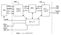
도 1은 일 실시예에 따라 마이크로컨트롤러 내에 집적될 수 있는 회로 내 디버그 모듈의 블록도를 도시한다. 그러나, 위에 설명된 바와 같은 일반적인 개념은 다른 유형들의 온-칩 디버그 회로부에 구현될 수 있다. 상기 블록도는 예를 들어 마이크로컨트롤러에 구현될 수 있고 그리고 다음과 같은 5개의 기본 블록들로 이루어질 수 있는 모듈을 보여준다:1 shows a block diagram of an in-circuit debug module that may be integrated into a microcontroller according to one embodiment. However, the general concept as described above can be implemented in other types of on-chip debug circuitry. The block diagram shows, for example, a module that can be implemented in a microcontroller and can consist of the following five basic blocks:
● 브레이크포인트 비교 로직(135)● Breakpoint comparison logic (135)
● 스톱-워치(Stop-Watch) 사이클 카운터 로직(150)Stop-watch
● 제어 및 상태 머신 로직(145)Control and
● 트레이스 로직(120)The trace logic (120)
● 이벤트 결합기 로직(125)
Event Combiner Logic (125)
CPU(110)는 내부 버스를 통해 하드웨어 브레이크포인트 유닛(135), 이벤트 검출 유닛(140), 제어 로직 유닛(145) 및 백그라운드 인터페이스(155)와 결합된다. 멀티플렉서(160)는 전용 디버그 클록 및 데이터 핀들(165)을 통해 디버그 유닛의 외부 디버거와의 결합을 가능하게 하는데 사용된다. 제어 로직(145)은 하나 이상의 외부 핀들과 결합될 수 있다. 도 1은 예시적인 TRGIN 핀(185)을 보여준다. 이러한 핀은 다른 기능이 전혀 없는 전용 핀일 수 있다. 그러나, 특히 로우(low)-핀 디바이스들에서, 이러한 핀은 프로그램 제어 하에 서로 다른 주변 디바이스들에 할당될 수 있는 다중-기능 핀일 수 있으며, 따라서 그의 프로그래밍된 할당에 따라 서로 다른 기능들을 수행할 수 있다. 예를 들어, 이러한 핀은 기능적으로 트레이스 트리거에 부가되도록 구성 레지스터에 의해 프로그래밍되어, 직렬 인터페이스 클록 핀, 디지털 I/O 핀, 아날로그 입력 핀 등으로서 동작할 수 있다. 도 1에 도시된 바와 같이, 제어 로직은 또한 핀(185)의 다중-기능 핀과 유사할 수 있는 트리거 출력 핀(190)을 제공한다. 트레이스 모듈(120)은 트레이스 스톨(stall) 입력 핀(115)과 트레이스 클록 및 데이터 출력 핀들(175)과 결합된다. 도 1은 또한 제어 로직(145)을 통해 구성 가능한 펄스 거부 필터들(170 및 180)을 도시한다. 이러한 필터들을 통한 신호 라우팅은 도 1에 도시되지 않았다. 몇몇 실시예들에 따르면, 브레이크포인트 디버깅은 "제로 스키드(zero skid)" 동작으로 불리는 명령어가 실행되기 전에 실행이 정지(halt)되도록 구현된다. 다른 디버거 실시예들에 따르면, 이것이 적용되지 않아서, 코드가 중지하거나 '스키드'하는 곳에서 프로세서가 정지되기 전에 명령어를 실행 가능하게 하는 문제들을 유발할 수 있다. 외부 이벤트들은 (정의상) 명령어 실행 스트림과 비동기적이다. 이를테면, 그들의 동작은 제로 스키드 개념들과 비교될 수 없다.
내부 신호 debug_en = 1일 때, 상기 모듈은 활성화되고, 모든 "HALT" 이벤트들을 모니터링하고, 이벤트들을 생성하고, 데이터 캡처를 수행하는 등을 행한다. 상기 내부 신호 debug_en = 0이면, 모든 디버그 로직은 비활성화되고, 상기 모듈은 최소의 전력 모드를 소비하도록 구성된다.When the internal signal debug_en = 1, the module is activated, monitoring all "HALT" events, generating events, performing data capture, and so on. If the internal signal debug_en = 0, all debug logic is deactivated and the module is configured to consume the minimum power mode.
디버깅을 덜 침입적(invasive)으로 행하기 위해서는, 실시간으로 디바이스의 외부로 데이터를 스트리밍하는 수단을 구비하는 것이 유용할 수 있다. 트레이스 모듈(120)은 판독되거나 특정 어드레스에 기록되는 데이터를 획득하여 트레이스 포트 외부로 송신하는 방법을 지원한다. 이는 실시간 워치포인트(watchpoint)라고 말할 수 있다. 상기 디바이스의 정상 동작은 워치포인트를 사용할 때 인터럽트되지 않는다.In order to make debugging less invasive, it may be useful to have means for streaming data out of the device in real time. The
데이터 캡처는 하드웨어 브레이크포인트를 생성하는데 사용되는 것과 동일한 하드웨어를 사용하여 수행될 수 있다. 홀트(halt) 생성과 동시에 데이터 캡처를 위한 브레이크포인트를 사용함으로써, 두 동작들 모두를 발생시킬 수 있을 것이다. 그러나, 데이터 캡처 및 데이터 매칭을 동시에 활성화하는 것은, 특히 하나보다 많은 브레이크포인트 카운트들에 대해서는, 예기치 않은 결과들을 발생시킬 수 있다. 데이터 캡처 및 데이터 비교가 동일한 물리 레지스터를 사용함에 따라, 비교 값은 모든 캡처에서 업데이트될 것이다.Data capture can be performed using the same hardware used to generate hardware breakpoints. By using a breakpoint for data capture at the same time as generating the halt, both operations will be generated. However, activating data capture and data matching at the same time can produce unexpected results, especially for more than one breakpoint count. As the data capture and data comparison use the same physical register, the comparison value will be updated in all captures.
도 2는 하드웨어 브레이크포인트 유닛(135)을 보다 상세하게 도시한다. 하드웨어 브레이크포인트들은 프로그램 및 데이터 메모리 중 어느 하나의 어드레스들의 매칭시 정지시키도록(break on) 구성될 수 있다. 이를 위해, 각각의 비교기들(220 및 230) 및 디코딩 유닛들(240)이 도 2에 도시된 바와 같이 제공된다. 브레이크포인트가 데이터 메모리 상에서 동작하도록 선택될 때, 상기 브레이크포인트는 부가적으로 데이터 값 및 마스크로 자격을 얻을 수 있어, 특정 값들만이 브레이크포인트 이벤트를 생성할 수 있게 한다. 또한, 데이터 브레이크포인트들은 단지 판독이나 기록 사이클들을 정지시키도록 임의로 설정될 수 있다. 모든 경우들에서, 브레이크포인트들은, 브레이크포인트 이벤트가 생성되기 전에 특정 이벤트가 N번 발생해야 하도록, 카운터(210)를 구비한다. 이 카운터(210)는 몇몇 실시예들에 따라, 예를 들어 1부터 256번까지의 임의의 값이 설정될 수 있다.Figure 2 shows the
도 2의 블록도는 단일 브레이크포인트에 대해 도시되었다. 그러나, 구현된 브레이크포인트들의 수는 다양한 실시예들에 따라 가변적이고, 많은 브레이크포인트들이 존재할 수 있다. 도 2는 다양한 파라미터들이 브레이크포인트를 위한 트리거 요구사항들을 정의하도록 프로그래밍될 수 있게 하는 예시적인 실시예를 보여준다. 다른 실시예들에 따르면, 보다 많거나 보다 적은 이러한 파라미터들이 사용될 수 있다. 예를 들어, 브레이크포인트를 발생시키는데 필요한 브레이크포인트 발생 횟수는 카운터(210)의 BPxCNT 파라미터에 의해 설정될 수 있다. 각각의 브레이크포인트 모듈은 동일한 레지스터들을 가질 수 있다.The block diagram of FIG. 2 is shown for a single breakpoint. However, the number of breakpoints implemented is variable according to various embodiments, and there may be many breakpoints. Figure 2 shows an exemplary embodiment that allows various parameters to be programmed to define triggering requirements for a breakpoint. According to other embodiments, more or less such parameters may be used. For example, the number of breakpoint occurrences required to generate a breakpoint may be set by the BPxCNT parameter of the
브레이크포인트들은 이벤트 채널 정의들 사이에 나열되며, 사이클 카운터(150)를 개시하거나 중지하는데, 이벤트 결합기 스테이지(125)를 설정하거나 재설정(리셋)하는데, 트레이스 유닛(120)을 개시하거나 중지하는데, 또는 스택 스냅샷(stack snapshot)을 획득하는데 사용될 수 있다.Breakpoints are listed among the event channel definitions and may be used to start or stop the
일 실시예에 따르면, 브레이크포인트가 활성화되기 위해서는 제어 레지스터 ICDBFxCON의 비트 BPEN이 설정되어야 한다. 이 비트가 소거되면, 이 특정 브레이크포인트에 대한 모든 회로부는 비활성화되고, 어떠한 브레이크포인트 이벤트도 생성되지 않을 것이다. 브레이크포인트는 자격 조건들의 모든 N번째 발생시에 소정 동작을 단지 트리거하도록 구성될 수 있다. 예를 들어, 매 세 번째 발생마다 트리거하도록 브레이크포인트를 설정하기 위해, 카운터(210)는 BPxCNT = 2로 설정된다. 각각의 제어 레지스터들은 그 값을 재로딩(reloading)하고/하거나 현재 상태를 모니터링하기 위해 카운터(210)와 결합하여 사용될 수 있다.According to one embodiment, the bit BPEN of the control register ICDBFxCON must be set for the breakpoint to be active. When this bit is cleared, all circuitry for this particular breakpoint will be inactive and no breakpoint event will be generated. The breakpoint may be configured to only trigger a certain operation at every Nth occurrence of the qualifications. For example, to set a breakpoint to trigger every third occurrence, the
또한, 브레이크포인트들은 예를 들어 연관된 구성 레지스터의 각각의 비트들을 설정함으로써 실행 컨텍스트(메인 라인 코드, 인터럽트 핸들러, 또는 둘 다)를 기반으로 자격이 부여될 수 있다. 브레이크포인트는 이후 프로그램이 선택된 컨텍스트로부터 실행중일 때에만 발생할 수 있다.Breakpoints may also be qualified based on the execution context (mainline code, interrupt handler, or both), for example, by setting the respective bits of the associated configuration register. A breakpoint can occur only when the program is running from a context that is subsequently selected.
구성 레지스터의 각각의 비트들을 설정함으로써, 프로그램 카운터(PC 실행 어드레스)를 모니터링할 수 있게 하는 다른 또 하나의 브레이크포인트 파라미터가 사용될 수 있다. 프로그램 메모리 브레이크들은 제로 스키드이며, 동작이 실행되기 전에 발생한다. PC는 트리거 명령어의 어드레스를 표시할 것이다.By setting each bit of the configuration register, another breakpoint parameter that allows monitoring of the program counter (PC execution address) can be used. Program memory brakes are zero skids and occur before the operation is executed. The PC will display the address of the trigger instruction.
각각의 제어 비트가 소거될 때, 예를 들어 BPAREN = '0'이면, 브레이크는 PC가 소정 어드레스와 동일할 때 트리거된다. BPAREN = '1'이면, 브레이크는 PC가 어드레스들의 소정 포함 범위에 들어갈 때 트리거된다.When each control bit is erased, for example, BPAREN = '0', the break is triggered when the PC is equal to the predetermined address. If BPAREN = '1', the break is triggered when the PC enters a predetermined inclusion range of addresses.
몇몇 실시예들에 따르면, 실행된 명령어들만이 브레이크포인트를 생성할 수 있다. PC가 실행되지 않는 어드레스에 있다면, 브레이크포인트는 트리거하지 않는다. 이는 다음을 포함한다:According to some embodiments, only executed instructions may generate a breakpoint. If the PC is at an unexecutable address, the breakpoint is not triggered. This includes:
● 흐름 변경 명령어들(CALL, RETURN 등),● Flow change commands (CALL, RETURN, etc.)
● 스킵 명령어들(per BTFSS, BTFSC), 또는● Skip commands (per BTFSS, BTFSC), or
● PCL, FSR 또는 다른 두 사이클 명령어들 이후의 다음 페치.
• Next fetch after PCL, FSR, or other two cycle instructions.
또 하나의 제어 비트 필드가 제어 레지스터에서 01, 10, 또는 11로 설정될 때, 브레이크포인트는 데이터 액세스들, 즉 어드레스 및 값 둘 다를 모니터링한다. 연관된 비트들의 세 가지 상태들은 판독 또는 기록 사이클들이 브레이크포인트를 결정하는데 사용되는지의 여부를 선택한다.When another control bit field is set to 01, 10, or 11 in the control register, the breakpoint monitors both data accesses, i.e., address and value. The three states of the associated bits select whether the read or write cycles are used to determine a breakpoint.
데이터가 (적용되는 것처럼) 판독되거나 기록된 후, 데이터 브레이크포인트들은 명령어 실행의 끝에서 필연적으로 브레이크를 일으킨다. 모든 경우들에서, 명령어는 완료될 때까지 실행된다. 따라서, "브레이크"는 실제로 다음 명령어 실행시 발생하고, 그리고 PC는 트리거 명령어 다음에 오는 명령어를 표시할 것이다. 또한, 브레이크는 메모리 어드레스와 데이터 값의 자격요건(qualifier)들이 둘 다 충족되었을 때 트리거될 수 있다.After the data is read or written (as applied), the data breakpoints inevitably break at the end of instruction execution. In all cases, the instruction is executed until completion. Thus, the "break" actually occurs upon execution of the next instruction, and the PC will display the instruction following the trigger instruction. The brakes can also be triggered when both the memory address and the qualifier of the data value are satisfied.
사이클 카운터(150)는 사용자 코드가 프로파일될 수 있도록, 스톱워치 기능을 제공하는데 사용되는 카운터이다. 사이클 카운터는 각각의 제어 레지스터들에 의해 제어된다. 카운터(150)는 네 개의 8-비트 카운터/레지스터들로 이루어질 수 있다. 카운터(150)는 CPU의 매 Q-사이클의 끝에서 증분될 수 있으며; 멀티-사이클 명령어들(예컨대, GOTO)은 여러 번 카운트한다.The
다수의 기능들이 특정 이벤트들에 의해 제어될 수 있도록 하기 위해, 가능한 모드 소스들은 하나의 이벤트 버스로 결합될 수 있다. 이는 사이클 카운터(150), 트레이스 유닛(120), 및 이벤트 결합기 유닛(125)이 이들의 동작들을 선택하기 위해 동일한 설정값들(settings)을 사용할 수 있게 한다.To enable multiple functions to be controlled by specific events, the possible mode sources can be combined into one event bus. This allows the
도 3에 도시된 바와 같은 이벤트 결합기(300)는 다수의 이벤트 입력들(320)을 모니터링하고, 그리고 그 입력들의 결합들 및 시퀀스들에 기초하여 정지(halt) 또는 트리거 출력(190)을 생성할 수 있다. 이벤트 결합기(300)는 각각의 제어 비트가 설정될 때 활성화된다. 비활성화된 결합기들(300)은 출력 이벤트들을 생성하지 않는다. 이벤트 결합기들(300)은 이벤트 채널 정의들 사이에 나열되고, 그리고 사이클 카운터(150)를 개시하거나 중지하는데, 이벤트 결합기 스테이지(310)를 설정하거나 재설정하는데, 트레이스 유닛(120)을 개시하거나 중지하는데, 또는 스택 스냅샷을 획득하는데 사용될 수 있다. 이벤트 결합기 스테이지들(310)은 그 스테이지에 대한 각각의 제어 비트들이 연관된 제어 레지스터들 내에 설정될 때 독립적으로 활성화된다. 스테이지의 현재 출력은 연관된 상태 비트에 반영될 것이다. 스테이지들(310)은 도 3에 도시된 바와 같이 묵시적인 순서를 가지며, 다음과 같은 다수의 방식들로 결합될 수 있다:The
● 스테이지는 하나의 이벤트에 의해 개별적으로 활성화될 수 있다,• Stages can be activated individually by one event,
● 스테이지는 다음의 낮은 스테이지가 활성인 동안 이벤트에 의해 활성화될 수 있다,• The stage can be activated by an event while the next lower stage is active,
● 스테이지는 하나의 이벤트에 의해 개별적으로 비활성화될 수 있다,• Stages can be deactivated individually by one event,
● 스테이지는 하나의 이벤트에 의해 또는 다음의 낮은 스테이지가 비활성화될 때 비활성화될 수 있다.
• The stage can be deactivated by one event or when the next lower stage is deactivated.
각각의 제어 비트를 설정함으로써, 결합된 이벤트(들)의 N+1번째 발생만이 출력 이벤트에 신호를 보낼 것이다. N은 0부터 255까지 설정될 수 있다. 결합된 트리거 조건들이 충족되면, 레지스터는 1씩 감분된다. 결합된 트리거 조건들이 충족되면, 이벤트 결합기 이벤트가 생성되고 그리고 카운터는 미리 설정된 값으로 재로딩(reloading)된다. 또한, 임의의 시간에 새로운 카운트 값이 각각의 제어 레지스터에 기록되고, 상기 카운터의 값은 재로딩된다. 예를 들어, 3번째 발생시에 트리거하도록 브레이크포인트를 설정하기 위해, 각각의 카운터 값은 2로 설정되어야 한다.By setting each control bit, only the (N + 1) th occurrence of the combined event (s) will signal the output event. N can be set from 0 to 255. If the combined trigger conditions are met, the register is decremented by one. If the combined trigger conditions are met, an event combiner event is generated and the counter is reloaded to a preset value. Also, at any time, a new count value is written to each control register, and the value of the counter is reloaded. For example, to set a breakpoint to trigger on the third occurrence, each counter value should be set to two.
게다가 몇몇 실시예들에 따르면, 핀 TRGIN(185)에 공급된 외부 신호는, 사용자 입력이 트레이스 스트림 내에 삽입될 트레이스 패킷들을 생성할 수 있게 하고, 정지들을 생성할 수 있게 하고 또한 임의로 트리거 TRGOUT 신호들을 생성할 수 있게 한다. "극성" = 0일 때(도 6), 트리거 입력은 액티브 하이(high)이고 상승 에지(edge)들은 이벤트들을 일으킨다. "극성" = 1일 때, 트리거 입력은 액티브 로우(low)이고 하강 에지들이 이벤트들을 일으킨다. 또 하나의 제어 비트는, 예를 들어 입력이 인식되기 위해 최소 시간 동안 액티브 상태에 있어야 함을 정의하기 위해, 필터를 제어하는데 사용될 수 있다. 이후 보다 짧은 펄스들이 무시된다.In addition, according to some embodiments, the external signal supplied to pin
TRGIN 이벤트는 이벤트 채널 정의들 사이에 리스트될 수 있고, 그리고 사이클 카운터(150)를 개시하거나 중지하는데, 이벤트 결합기 스테이지(310)를 설정하거나 재설정하는데, 트레이스 유닛(120)을 개시하거나 중지하는데, 또는 스택 스냅샷을 획득하는데 사용될 수 있다. 트리거 입력의 변화들은 트레이스가 활성화되면 트레이스 패킷을 생성할 것이다.The TRGIN event may be listed between event channel definitions and may be used to start or stop the
브레이크포인트 같은 이벤트가 인에이블된 트리거에 의해 발생할 때, TRGOUT 핀(195)에 펄스가 생성된다. 기본 트리거 출력 신호 동작은 각각의 제어 비트들을 설정함으로써 구성된다. 이 제어 비트들은 예를 들어, 트리거 출력이 대략 트리거 이벤트의 지속기간 동안 어서트(assert)되는 것을 제어할 수 있다. 인접하거나 혹은 중첩하는 이벤트들은 신호를 어서트된 상태로 유지할 수 있다. 상기 제어 비트들은 또한 출력이 최소 시간 주기로 스트레칭(stretching)되는지의 여부를 제어할 수 있다. TRGOUT 원샷이 트리거되면, 시간 주기 내에 발생하는 더 많은 이벤트들이 무시될 것이다. 상기 원샷이 타임 아웃되고 TRGOUT가 제로(zero)로 귀환한 후, 그것은 또 하나의 이벤트에 의해 다시 트리거될 수 있다. 상기 원샷은 에지 트리거되고, 그리고 이벤트 신호가 지속되더라도 소정 시간 주기 이후 소거될 것이다.When an event such as a breakpoint is triggered by an enabled trigger, a pulse is generated on the TRGOUT pin 195. The basic trigger output signal operation is configured by setting the respective control bits. These control bits can, for example, control that the trigger output is asserted for the duration of the trigger event. Adjacent or overlapping events can keep the signal asserted. The control bits may also control whether the output is stretched to a minimum time period. When the TRGOUT one shot is triggered, more events occurring within the time period will be ignored. After the one-shot times out and TRGOUT returns to zero, it can be triggered again by another event. The one shot will be edge triggered and will be erased after a predetermined time period even if the event signal persists.
소프트웨어는 각각의 제어 비트를 설정함으로써 트리거 아웃을 일으킬 수 있다. 디바이스가 깨어 있으면, 비트는 1 사이클 이후 하드웨어에 의해 소거된다. TRGOUT는 또한 각각의 제어 비트를 기록함으로써 소거될 수 있거나, 또는 디바이스가 깨어나면 자동으로 소거될 것이다.The software can trigger out by setting each control bit. If the device is awake, the bit is cleared by the hardware after one cycle. TRGOUT can also be cleared by writing each control bit, or it will automatically be cleared when the device wakes up.
외부의 비동기식 리셋들은 전형적으로 전체 프로세서 디바이스에 영향을 미친다. 이러한 이벤트가 발생했음을 정확하게 기록하기 위해, 명령어 트레이스 모듈은 리셋의 타이밍과는 무관하게 리셋에 의한 영향을 받지 않도록 설계된다. 따라서, 다양한 실시예들은 온(on)-칩 디버그 기능들을 향상시키고, 이전에 종래의 마이크로컨트롤러 디바이스들에서는 이용할 수 없었던 특징들을 제공한다. 따라서, 단지 고가의 전용 회로 내 디버거들과 일반적으로 구별되는 첨단 디버깅 기능들은 "정상" 마이크로컨트롤러 또는 마이크로프로세서 디바이스들에 구현될 수 있다.External asynchronous resets typically affect the entire processor device. To accurately record the occurrence of these events, the instruction trace module is designed to be unaffected by the reset regardless of the timing of the reset. Thus, various embodiments improve on-chip debug functions and provide features that were not previously available in conventional microcontroller devices. Thus, advanced debugging functions, which are generally distinguished from those only in expensive dedicated circuit debuggers, can be implemented in "normal" microcontroller or microprocessor devices.
도 4는 다양한 실시예들에 따른 고레벨 개념을 도시한다. 시스템 클록 구성 모듈(410)은 시스템 클록(icd_sys_clk)을 생성한다. 시스템 클록은 trc_q_clks 신호들, 즉 trc_ql_clk, trc_q2_clk, trc_q3_clk 및 trc_q4_clk의 4개의 위상들을 생성하는 트레이스 Q-발생기(420)에 의해 사용된다. 도 11은 명령어 실행에 관하여 시스템 클록(clkin) 및 관련 쿼드러처 신호들의 예시적인 타이밍도를 도시한다. 이 실시예에서는, clkin으로부터 유도된 4개의 클록들(q1, q2, q3, q4)이 하나의 명령어를 실행하는데 사용된다. 트레이스 클록들은 내부 클록들(q1, q2, q3, q4)로부터 유도될 수 있거나, 또는 이 클록들과 동일할 수 있다. 그러나, 다른 실시예들에 따르면, 예를 들어 단일 사이클 내의 명령어들을 실행시킬 수 있는 다른 중앙 처리 아키텍처가 구현될 수 있다.Figure 4 illustrates a high-level concept in accordance with various embodiments. The system
도 5는 트레이스 Q-발생기(420)의 개략도의 세부사항들을 도시한다. 트레이스 Q-발생기는 예를 들어 기존 방식으로 4개의 플립-플롭들(510, 520, 530 및 540)에 의해 형성된 4-비트 순환 시프트 레지스터일 수 있다. 리셋 소스들의 몇 가지 예들은 다음과 같다: 워치독 타이머(watchdog timer; WDT) 리셋, 중앙 처리 유닛에 의해 실행된 RESET 명령어, 스택 오버플로우/언더플로우 리셋 및 마스터 클리어(master clear; MCLR) 리셋. 그러나, 다른 리셋 소스들 및 신호가 적용될 수 있다.5 shows the details of a schematic diagram of trace Q-
도 4를 다시 보면, 일반 리셋이 발생할 때, 리셋 아날로그 유닛(430)은 일반 리셋이 시스템 클록 구성 모듈(410)을 제외한 전체 칩에 어서트될 수 있게 한다. 이는 시스템 클록이 계속 실행될 수 있게 하고, 트레이스 Q-발생기(420) 및 따라서 또한 트레이스 데이터 발생기(120)는 계속 동작할 수 있다. 마이크로컨트롤러 중앙 처리 유닛(110)이 리셋으로 유지되는 동안, 트레이스 데이터 발생기는 리셋 관련 트레이스 정보를 기록하고, 이후 트레이스 Q-발생기에게 상기 기록이 수행되었음을 알린다.4, when a general reset occurs, the
일반 리셋 조건은 또한, 예를 들어 플립-플롭들(450 및 460)에 의해 각각 trc_q2_clk 신호 및 trc_q4_clk 신호를 이용하여 동기화되고, 그리고 트레이스 Q-발생기(420)가 중지할 때, 리셋 아날로그 유닛(430)은 예를 들어 플립-플롭(480)에 의해 통지되어 시스템 클록 구성 모듈(430)이 리셋될 수 있게 한다.The general reset condition is also synchronized using, for example, the trc_q2_clk signal and the trc_q4_clk signal by flip-
리셋 아날로그 유닛(430)의 예시적인 실시예는 도 6에 도시되어 있다. 리셋 아날로그 유닛(430)은 시스템 클록 구성 모듈(410)이 리셋될 수 있게 하는데, 다만 이렇게 하도록 통지를 받은 후에 가능하다. 상기 시스템 클록 구성 모듈(430)이 리셋됨과 동시에, 원-샷 플러스 trc_reset_osl_pulse가 생성되어 동기화기 레지스터 요소들(450, 460, 480)을 리셋하고, 이에 따라 전체 회로는 또 하나의 리셋 발생 검출을 위해 재장비될(re-armed) 수 있다. 도 6에 도시된 바와 같이, 로직은 여러 제어 신호들을 생성하도록 제공될 수 있다. 디바이스의 일반 설계에 따라, 다른 로직 회로들이 사용되고 적응될 수 있다.An exemplary embodiment of the
따라서, 이 다양한 실시예들은 레벨 민감성 리셋 및 에지 민감성 리셋을 둘 다 처리할 수 있는 기능을 가지며, 그리고 리셋이 발생하자마자 (시스템 클록 구성 모듈을 제외한) 전체 마이크로컨트롤러 시스템이 리셋될 수 있게 하고, 따라서 명령어 트레이스가 진행되는 경우에도 네이티브 동작에 더 가깝게 한다.Thus, these various embodiments have the ability to handle both level sensitive reset and edge sensitive reset, and allow the entire microcontroller system (except the system clock configuration module) to reset as soon as a reset occurs, So that it becomes closer to the native operation even when the instruction trace proceeds.
다양한 실시예들은 최소 펄스 폭 지속기간이 시스템 클록 구성 모듈을 리셋하도록 보증됨을 보장하는데, 상기 모듈이 칩 리셋이 발생하자마자 리셋되는 것으로부터 방지되어 있다고 하더라도 그러하다.Various embodiments ensure that the minimum pulse width duration is guaranteed to reset the system clock configuration module, even if the module is prevented from resetting as soon as a chip reset occurs.
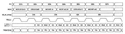
다음 절에서는, 디바이스와 외부 디버그 툴 사이의 트레이스 데이터 인터페이스를 상세히 설명한다. 도 7에 예를 들어 도시된 바와 같은 트레이스 서브시스템은, 디버그 툴에 의해 캡처되고 분석될 수 있는 명령어 실행 스트림의 실시간 기록을 제공한다. 트레이스 동작은 디버그 툴이 소스 코드 및 프로그램 메모리 콘텐츠에 액세스하였고 그리고 CPU 동작의 몇몇 양상들을 추론할 수 있다고 가정한다.In the following sections, the trace data interface between the device and the external debug tool is described in detail. The trace subsystem as illustrated in FIG. 7, for example, provides a real-time record of the instruction execution stream that can be captured and analyzed by the debug tool. The trace operation assumes that the debug tool has access to the source code and program memory contents and can infer some aspects of CPU operation.
명령어가 PCL에 (직접 또는 INDx를 통해) 기록할 때, 새로운 PC는 프로그램 메모리에 어디든지 있을 수 있다. 이 경우, 명령어 패킷은 소위 전체 프로그램 카운터(full program counter; FPC) 패킷으로 대체된다. 도 7에 도시된 바와 같은 FIFO는 코어 데이터 레이트를 (TRSTALL에 의해 지배되는) 디버그 툴 데이터 레이트와 매칭시키는데 사용될 수 있다. FIFO는 CPU 인코더로부터 채워지고, 도 7에 도시된 바와 같이, 데이터 인코더에 의해 비워진다. FIFO는 최대 4096 명령어 패킷들을 보유하지만, 효과적인 운영 사이즈는 각각의 제어 비트들에 의해 선택될 수 있다. WATCH 이벤트 패킷들은 또한 FIFO 내에 배치되어서, 실제 인플라이트(in-flight) 명령어 패킷들의 수는 보통 적을 것이다. 토글링할 때, TRCLK 출력은 각각의 클록 에지에 따라 하나의 데이터 워드를 출력한다. 출력 클록 레이트는 항상 CPU 명령어 레이트에 링크되고, 그리고 소프트웨어가 SYSCLK를 변경시키거나 리셋이 SYSCLK를 변경시키면 변화할 것이다. 각각의 구성에 따르면, 출력 레이트는 항상 명령어 주기당 두 개의 트레이스 워드들일 수 있다. 상기 레이트는 명령어당 1 및 1/2로 감소할 수 있지만, 이로써 FIFO 오버플로우를 야기시킬 것이다. TRCLK 출력은, TRCPS 비트들의 설정에 따라, 데이터 변화들과 같은 위상이거나 다른 위상이도록 선택될 수 있다. FIFO 내 인코딩은 라인 인코딩과 상이할 수 있어서, 각각의 FIFO 위치는 TRDAT 인터페이스 내에 무려 3개나 되는 데이터 워드들을 나타낼 수 있다.When a command is written to the PCL (directly or via INDx), the new PC can reside anywhere in the program memory. In this case, the instruction packet is replaced with a so-called full program counter (FPC) packet. The FIFO as shown in FIG. 7 can be used to match the core data rate with the debug tool data rate (as governed by TRSTALL). The FIFO is populated from the CPU encoder and emptied by the data encoder, as shown in FIG. The FIFO holds up to 4096 instruction packets, but an effective operating size can be selected by each control bit. WATCH event packets are also placed in the FIFO, so the actual number of in-flight instruction packets will usually be less. When toggling, the TRCLK output outputs one data word according to each clock edge. The output clock rate is always linked to the CPU command rate and will change if the software changes the SYSCLK or the reset changes the SYSCLK. According to each configuration, the output rate may always be two trace words per instruction cycle. The rate can be reduced to one and one half per instruction, but this will cause a FIFO overflow. The TRCLK output may be selected to be the same phase or different phase as the data changes, depending on the setting of the TRCPS bits. The encoding in the FIFO may differ from the line encoding so that each FIFO location can represent as many as three data words in the TRDAT interface.
트레이스 스톨(stall) 기능이 구현될 수 있으며, 여기서 구성 비트는 TRSTALL 입력이 효과를 나타내는지의 여부를 결정할 수 있다. 예를 들어, 제어 비트 TRXSE = 1이고 신호 TRSTALL = 1일 때, 트레이스 FIFO는 페이로드 경계(payload boundary)에서 비우기를 중지하고 클록을 중단할 것이다. TRSTALL(tr_stall_pin)이 '0'으로 귀환할 때, 클록킹은 재개될 것이고 FIFO는 데이터를 다시 비우기 시작할 것이다. 트레이스가 인에이블되고 FIFO가 비어있을 때, IDLE 또는 SLEEP 패킷들은 디바이스의 슬립(sleep) 상태에 따라 전송된다. 몇몇 실시예들에 따라 FIFO는 또한 강제로 비워질 수 있고, 트레이스는 비활성화될 수 있다. FIFO가 가득 차게 되면, 시스템 응답은 각각의 제어 설정에 의존할 수 있다. 여하튼, (스톨된(stalled) 또는 데이터를 포스팅(posting)하지 않는) 오버플로우 상태는, FIFO가 각각의 제어 레지스터에 의해 선택된 대로 25% 또는 75%로 가득 찰 때까지 지속될 것이다. 몇몇 실시예들에 따라, 트레이스 구현에 관한 다른 기능들이 부가될 수 있고, 그리고 개시된 바와 같은 몇몇 기능들은 구현되지 않을 수 있다. 전형적인 트레이스 신호 타이밍도가 도 8에 도시되어 있다.A trace stall function may be implemented, wherein the configuration bit may determine whether the TRSTALL input represents an effect. For example, when the control bit TRXSE = 1 and the signal TRSTALL = 1, the trace FIFO will stop emptying at the payload boundary and stop the clock. When TRSTALL (tr_stall_pin) returns to '0', the clocking will be resumed and the FIFO will start emptying the data again. When tracing is enabled and the FIFO is empty, IDLE or SLEEP packets are transmitted according to the sleep state of the device. According to some embodiments, the FIFO may also be forced to be emptied, and the trace may be deactivated. Once the FIFO is full, the system response may depend on each control setting. Anyway, an overflow condition (stalled or not posting data) will last until the FIFO is full at 25% or 75% as selected by each control register. According to some embodiments, other functions related to trace implementation may be added, and some functions as disclosed may not be implemented. A typical trace signal timing diagram is shown in FIG.
트레이스 페이로드 패킷들은, CPU 코어가 실행하는 명령어들 및 선택된 데이터 이벤트들을 인코딩하고, 또한 트레이스 스트림 동기화를 제공한다. 일 실시예에 따르면, 대부분의 패킷들은 1개 또는 2개의 7-비트 워드들로 이루어질 수 있고, 또는 FPC 패킷에 대해서는 3개의 워드들로 이루어질 수 있다. 일반적으로 말해서, 패킷들은 "워드 1" 및 임의의 "워드 2"로 이루어진다. 그러나, 또 다른 실시예들에 따라 다른 포맷들이 사용될 수 있다. 특정 실시예에 따르면, "워드 1"의 값은 패킷을 확인하고, "워드 2"가 존재하는지의 여부를 암시한다. (EX, EXD, 및 RESET과 같은) 명령어 실행과 동기하는 패킷들 및 비동기 "이벤트" 패킷들은 아래에 보다 상세히 개시되는 바와 같이 WATCH, RESET, 및 TRIGGER를 포함한다.The trace payload packets encode the instructions and selected data events that the CPU core executes and also provide trace stream synchronization. According to one embodiment, most packets may consist of one or two 7-bit words, or three words for an FPC packet. Generally speaking, the packets are made up of "
동기화 패킷들은 실행 순서대로 방출된다. 이벤트 패킷들은 이벤트 시간 부근의 스트림에 나타나지만, 다수의 이벤트들이 동시에 일어나면, 몇몇 보고들은 지연될 것이다. 몇몇 경우들에서는, FPC가 동기화 보고이지만, 다른 때에는 FPC가 이벤트이다. 전송 층(transport layer; TR) 패킷들(RESYNC, IDLE 및 END)은 필요에 따라 삽입되어 인터페이스 데이터 스트림의 여러 상태들을 관리하고 확인한다. TR 패킷들(RESYNC 및 IDLE)은 명령어 트레이스를 분석할 때 버려질 수 있다.The synchronization packets are emitted in the order of execution. Event packets appear in the stream near the event time, but if multiple events occur simultaneously, some reports will be delayed. In some cases, the FPC is a synchronization report, but at other times the FPC is an event. The transport layer (TR) packets (RESYNC, IDLE, and END) are inserted as needed to manage and verify various states of the interface data stream. TR packets (RESYNC and IDLE) can be discarded when analyzing instruction traces.
RESYNC 패킷들은 각각의 제어 비트들에 의해 특정된 대로 주기적으로 삽입되고, 그래서 수신기는 RESYNC 패킷들이 올바르게 동기화되어 있는지 확인할 수 있다. 때때로 소정 시간 간격에 대략 대응하고, 그리고 어떠한 다른 FPC도 상기 간격 내에서 전송되지만 않았다면, FPC는 상기 스트림에 부가될 것이다. 이는 수신기가 올바르게 명령어 스트림을 추적하고 있다는 체크를 제공한다. 삽입된 FPC들은 항상, 다음에 오는 명령어의 어드레스를 표시한다. 패킷 내의 워드들의 수는 패킷 워드 1의 값에 의해 결정된다. RESYNC가 "워드 2"에 대해 틀린 값을 갖는 워드 1로서 수신되면, 스트림은 아웃 오브 싱크(out of sync)이고 에러는 플래그되어야 한다.The RESYNC packets are periodically inserted as specified by the respective control bits, so that the receiver can verify that the RESYNC packets are correctly synchronized. Sometimes it corresponds roughly at certain time intervals, and if no other FPC has been transmitted within the interval, an FPC will be added to the stream. This provides a check that the receiver is correctly tracking the instruction stream. The inserted FPCs always indicate the address of the next instruction. The number of words in a packet is determined by the value of
표 1은 RESYNC가 다음에 오는, 제 2 워드가 0x7D인 2-워드 패킷을 포함하는 최악의 경우의 상황을 나타낸다. 수신기가 적당히 동기화되면, 수신된 워드 #3는 워드 1일 것이고, 워드 #4는 워드 2일 것이고, 패킷 #2로서 도시되는 완전한 RESYNC 쌍을 형성할 것이다. 패킷 #3은 워드 #5로 시작되고, 올바르게 해석될 것이다.Table 1 shows the worst case situation in which RESYNC comes next and a second word contains a 2-word packet of 0x7D. If the receiver is properly synchronized, the received

표 2는, 제 1 워드를 복제하고 수신기를 아웃 오브 싱크로 만드는 클록-바운스(clock-bounce)를 갖는 동일한 데이터를 보여준다. 워드 #1 및 워드 #2는 데이터=0x71를 갖는 EXD 패킷으로서 수신되고(하지만 이는 틀린 해석이다), 워드 #3 및 워드 #4는 RESYNC 쌍처럼 나타난다. 워드 #5는 새로운 RESYNC 패킷의 워드 1로서 취해지지만, 워드 #6은 0x7D가 아니고, 동기화되지 않은 상태로 나타난다. 워드 #6은 새로운 패킷을 개시한다.Table 2 shows the same data with a clock-bounce that replicates the first word and makes the receiver out-of-sync.

트레이싱이 개시될 때, 또는 디버그 실행을 위해 일시 중단된 후 트레이싱이 재개할 때, 전송된 제 1 패킷은 항상 FPC일 것이다. 전체 프로그램 카운터(FPC) 패킷은 스트림에 나타나는 다음 명령어의 절대 주소를 보고한다.When tracing is started, or when tracing resumes after being suspended for debug execution, the first packet transmitted will always be an FPC. The entire program counter (FPC) packet reports the absolute address of the next instruction appearing in the stream.
― 트레이스의 개시,- start of trace,
― 오버플로우 후의 재개, 및- resuming after overflow, and
― 디버그 후의 재개- Resume after debug
의 이 상황들에서의 FPC 보고는 단순히 다음 명령어의 주소를 표시한다.The FPC report in these situations simply indicates the address of the next instruction.
FPC의 다른 모든 이용들은 명령어가 실행되었음을 표시하고, 몇몇 경우들에서는 그 명령어에 대해 보고되었어야 할 패킷을 대신한다. FPC가 분기(branch) 또는 프로그램 카운터 변경 명령어들의 실행을 나타낼 때, 보고된 값은 분기 타겟 주소이다. FPC 다음에 오는 명령어 패킷은 FPC가 가리키는 명령어의 실행을 나타낸다.All other uses of the FPC indicate that the command has been executed and, in some cases, replace the packet that should have been reported for that command. When the FPC indicates execution of a branch or program counter change commands, the reported value is the branch target address. The instruction packet following the FPC indicates the execution of the instruction indicated by the FPC.
GOTO 및 CALL 명령어들은, 프로그램 카운터 PC[10:0]의 최하위 비트들이 (어셈블리 코드의) 디버그 환경에 알려져 있고, 새로운 PC의 상위 4 비트들만이 상부 일부분 프로그램 카운터(upper partial program counter; UPC) 패킷에 보고된다고 가정한다. 그러나, 다른 실시예들은 보다 많거나 보다 적은 정보를 보고할 수 있다. 보고된 값은 0x0F & (PCLATH >> 3)일 수 있고, 여기서 PCLATH는 프로그램 카운터의 상위 비트들을 래칭(latching)하는 구현 특정 레지스터를 나타낸다. 관련 브랜치(BRA)들의 목적지가 소스 코드에 알려져 있기 때문에, 명령어는 단순히 EX로서 보고된다. 매우 다양한 트레이스 페이로드들이 구현될 수 있다. 표 3는 서로 다른 페이로드 신호들의 예를 보여준다.GOTO and CALL instructions are used to determine if the least significant bits of the program counter PC [10: 0] are known in the debug environment (of assembly code) and only the upper four bits of the new PC are upper part program counter (UPC) . ≪ / RTI > However, other embodiments may report more or less information. The reported value may be 0x0F & (PCLATH >> 3), where PCLATH represents an implementation specific register that latches the upper bits of the program counter. Since the destination of the relevant branch (BRA) is known to the source code, the instruction is simply reported as EX. A wide variety of trace payloads can be implemented. Table 3 shows examples of different payload signals.

표 4는 실제 트레이스의 예를 보여준다.Table 4 shows examples of actual traces.

트리거 입력의 변화들은 각각의 제어 비트가 설정되어 있는 경우 트레이스 패킷을 생성할 것이다. 극성 비트 = 0이면, 이벤트는 상승 에지에서 트리거할 것이다. 극성 비트 = 1이면, 이벤트는 하강 에지에서 트리거할 것이다. 명령어가 프로그램 카운터 PCL에 직접적으로 또는 간접적으로 기록할 때, 새로운 PC는 프로그램 메모리에 어디든지 있을 수 있다. 이 경우, 명령어 패킷은 FPC 패킷으로 대체된다.Changes in the trigger input will generate a trace packet if each control bit is set. If the polarity bit = 0, the event will trigger on the rising edge. If the polarity bit = 1, the event will trigger on the falling edge. When an instruction writes directly or indirectly to the program counter PCL, a new PC can reside anywhere in the program memory. In this case, the instruction packet is replaced with an FPC packet.
FIFO는 코어 데이터 레이트를 (TRSTALL에 의해 지배되는) 디버그 툴 데이터 레이트와 매칭시키는데 사용된다. FIFO는 CPU 인코더로부터 채워지고, 도 6에 도시된 바와 같이, 데이터 인코더에 의해 비워진다. FIFO는 최대 4096 명령어 패킷들을 보유하지만, 효과적인 운영 사이즈는 제어 레지스터 내의 각각의 비트들에 의해 선택된다. WATCH 이벤트 패킷들은 또한 FIFO 내에 배치되어서, 실제 인플라이트(in-flight) 명령어 패킷들의 수는 보통 적을 것이다.The FIFO is used to match the core data rate with the debug tool data rate (governed by TRSTALL). The FIFO is populated from the CPU encoder and emptied by the data encoder, as shown in FIG. The FIFO holds up to 4096 instruction packets, but the effective operating size is selected by each bit in the control register. WATCH event packets are also placed in the FIFO, so the actual number of in-flight instruction packets will usually be less.
토글링할 때, TRCLK 출력은 각각의 클록 에지에 따라 하나의 데이터 워드를 출력한다. 출력 클록 레이트는 항상 CPU 명령어 레이트에 링크되고, 그리고 소프트웨어가 SYSCLK를 변경시키거나 리셋이 SYSCLK를 변경시키면 변화할 것이다. 연관된 제어 레지스터의 각각의 비트 필드가 설정될 때, 출력 레이트는 항상 명령어 주기당 두 개의 트레이스 워드들일 수 있다. 상기 레이트는 명령어당 1 및 1/2로 감소할 수 있지만, 이로써 몇몇 실시예들에 따르면 FIFO 오버플로우를 야기시킬 것이다. 트레이스 클록(TRCLK) 출력은, 각각의 제어 비트들의 설정에 따라, 데이터 변화들과 같은 위상이거나 다른 위상이도록 선택될 수 있다. FIFO 내 인코딩은 라인 인코딩과 상이해서, 각각의 FIFO 위치는 TRDAT 인터페이스 내에 무려 3개나 되는 데이터 워드들을 나타낼 수 있다.When toggling, the TRCLK output outputs one data word according to each clock edge. The output clock rate is always linked to the CPU command rate and will change if the software changes the SYSCLK or the reset changes the SYSCLK. When each bit field of the associated control register is set, the output rate can always be two trace words per instruction cycle. The rate may be reduced to 1 and 1/2 per instruction, but this will cause a FIFO overflow according to some embodiments. The trace clock (TRCLK) output may be selected to be the same phase or different phase as the data changes, depending on the setting of the respective control bits. Since the encodings in the FIFO are different from the line encodings, each FIFO location can represent as many as three data words in the TRDAT interface.
도 9는 트레이스 서브(sub) 시스템(700)의 단순화된 블록도를 도시한다. 서브시스템(700)은 코어 및 WATCH 이벤트 신호들로부터 명령어 코드들을 수신하고, TRDAT 신호들 상의 전달을 위해 이 데이터를 포맷한다. 시퀀스 제어기(710)는 명령어 및 WATCH 데이터를 FIFO에 로딩할 책임이 있다. 각각의 데이터 패킷은 단일 16-비트 워드로서 인코딩된다. q34동안, WATCH 신호들은 샘플링되고, 가장 높은 우선 순위의 신호가 인코딩되고, 로딩되고 그리고 리셋된다. 2 이상의 신호가 어서트되면, 가장 높은 우선순위의 신호만이 로딩되고, 나머지 다른 신호들은 이후의 q34 기회들을 기다려야 한다. 보고 우선순위가 브레이크포인트 넘버를 기반으로 하기 때문에, 이벤트들은 순서와 다르게 보고될 수 있다. q12 동안에는 이전 명령어로부터의 데이터가 인코딩되고 로딩된다(q3에서는 연산 코드가 인코딩되고, 버스 데이터는 안정적인 q3-q3이고, 그리고 모두는 상승 q1에서 유효하다). 일반적으로 말해서, 이것은 모든 명령어 주기에서 발생한다. 분기 및 호출 명령어들에 대해서는, 인터럽트 사이클들뿐만 아니라, 제 1 사이클 동안에는 아무것도 로딩되지 않으며, 패킷은 제 2 사이클 동안 인코딩되어(소위 "강제된 NOP"), UPC 및 FPC가 정확한 PC 값으로 방출될 수 있게 한다. 결과적으로, 두 WATCH 패킷들은 분기 동안 로딩될 수 있다. SKIP 및 STALL은 현재의 코어 동작을 기반으로 인코딩된다.FIG. 9 shows a simplified block diagram of a
시퀀스 제어기(710)는 명령어 사이클마다 두 번 로딩할 수 있고 스트림 관리자(730)는 명령어 사이클마다 두 번 언로딩(unloading)할 수 있어, 명령어 사이클마다 최대 4개의 메모리 사이클들을 필요로 할 수 있다. FIFO 제어기(720)는 시퀀스 제어기(710)에 의해 제공된 데이터를 관리한다. 데이터는 스트림 관리자(730)에 의해 요청될 때 동일한 순서로 전달된다. 스트림 관리자(730)는 16-비트 FIFO 워드들을 TRDAT 신호들 상에서 송신되는 데이터 워드들 내에 재포맷한다. 일부 패킷들(예컨대, EX)은 각각의 FIFO 워드에 대해 단일 TRDAT 워드를 생성하지만, 다른 패킷들(예컨대, FPC)은 그보다 많이 생성한다. 필요에 따라, 전송 관리 패킷들(RESYNC, IDLE 및 END)이 스트림 내에 삽입되고, 그리고 판독 동작은 TRSTALL 입력에 따라 일시 정지된다. 각각의 명령어 사이클 주기 동안에는, 2개의 TRDAT 워드들이 전송된다. TRCLK 신호는 시스템 리셋 동안 (사이클의 스트레치(stretch) 부분을) 일시 정지할 것이다(데이터는 손실되지 않을 것이다).
도 10은 트레이스 수신기로서 동작하는 디버그 툴(820)과 결합된 다양한 실시예들에 따른 마이크로컨트롤러(810)를 갖는 시스템(800)을 도시한다. 디버그 툴은 예를 들어, 출원인에 의해 제조된 회로 에뮬레이터의 리얼(Real)-ICE일 수 있다. 수신기(820)는 트레이스 동기화를 수행하고, 모든 IDLE 및 전송 패킷들을 버리고, 남은 패킷들의 번들(bundle)들을 원격 호스트(830) - 예를 들어, 패킷 스트림 해석이 수행되는 퍼스널 컴퓨터 또는 워크 스테이션 - 로 송신한다.Figure 10 shows a
● 워드 1 분석 ― 패킷들을 3-워드 폭의 데이터 버스로 변환한다.●
● 더블릿(doublet)들(RESYNC, OVERFLOW 등)을 검사하고, 그리고 (a) 더블릿들이 연속적인 워드들에 없을 때, 또는 (b) 미구현된 워드 1 코드 값이 나타날 때, 동기화 에러들을 플래그(flag)한다.Checking for doublets (RESYNC, OVERFLOW, etc.), and (a) when the doublets are not in consecutive words, or (b) when the word value of the
● IDLE 및 다른 전송 패킷들을 버리고, 그리고 남은 값들을 FIFO에 스택(stack)한다.● Discard IDLE and other transport packets and stack the remaining values into the FIFO.
● 전체 패킷들을 원격 호스트에 송신한다.
• Send all packets to the remote host.
TRSTALL을 어서트할 때, 수신기(820)는 재동기화 파이프라인에 인큐잉(en-queueing)될 수 있는 2개의 워드들을 더하여 최대 6개 더 많은 TRDAT 워드들(2개의 연속적인 FPC 패킷들의 상당물)을 받아들이도록 준비된다. TRSTALL을 해제할 때, 패킷 워드 1 정렬이 보장된다. IDLE 패킷들의 스트링으로부터, 대부분이 또는 때때로 모두가 버려져서 원격 호스트에 발송되지 않아 대역폭을 줄일 수 있다. 미구현된 연산 코드들 및 FPC 워드 3(7'h5x)은 또한 동기화 에러들로서 플래그되어야 하고 1-워드 패킷들로서 취급되어야 한다.When asserting TRSTALL, the
FPC의 제 3 워드는 단일-워드 패킷의 스타일(예컨대, 코드 7'h5x)로 인코딩된다. 동기화 여부에 상관없이, 예를 들어 7'h5x의 임의의 워드 다음에 오는 워드는 새로운 패킷의 워드 1이라고 가정될 수 있다. 워드 1을 추적하는 목적을 위해, OVERFLOW, RESYNC, SLEEP 및 END 패킷들은 1-워드 패킷들로서 취급되어야 한다. 7'h7D가 1-워드 패킷으로서 취급될 때, 이후 다음의 패킷은 또 하나의 7'h7D(한 쌍의 RESYNC 워드)이더라도 항상 워드 1의 값일 것이다. 워드 1-정렬 (의사(pseudo)) 데이터는 더블릿 분석에 전달되고, 더블릿 분석에서는 두 RESYNC가 스트림에 연속적으로 나타나지 않을 때 동기화 실패가 인식된다. 이와 마찬가지로, OVERFLOW(7'h77)는 수신기가 아웃 오브 싱크일 때 나타날 수 있으며, 제 2 워드가 매칭되지 않더라도 정확히 해석되어야 한다. 이는 또한 동기화 에러를 플래그할 수 있다. 유사한 추론이 SLEEP 및 END 패킷들에 적용될 수 있는데, 왜냐하면 수신기가 아웃 오브 싱크이면, 단지 하나의 7'h7C 또는 7'h7F가 끝에 나타날 수 있고, 수신기가 제 2 값을 대기하는 동안 중단되는(hanging) 것이 부적합할 것이기 때문이다. 이와는 정반대로, 3개의 동일한 워드들이 나타날 수 있는데, 어느 것도 수신기를 혼동하지 말아야 한다.The third word of the FPC is encoded in the style of a single-word packet (e.g., code 7'h5x). Regardless of the synchronization, the word following any word, for example 7'h5x, can be assumed to be
완벽한 분석을 위해, 호스트(830)는, 트레이스 데이터를 마이크로프로세서를 프로그래밍하는데 사용된 오리지널 소스 코드와 비교해야 한다. 대부분의 명령어들에 대해, 트레이스 데이터는 실행이 발생했음을 선언하지만, 동작 세부 사항들은 포함되지 않는다. 분기(branch)들이 EX 패킷들(TRFPCB = 0)만을 생성할 때, 분기 목적지는 단지 소스 코드를 검사함으로써 결정될 수 있다. 유사하게, 특정 실시예에 따르면, PCLATH에의 기록은 단지 부분적인 데이터만을 방출하고, 그리고 평가를 완료하기 위해 소스 지식을 필요로 한다. 동작에 의존하여, STALL 패킷들은 영향을 받는 명령어에 선행하거나 뒤따를 수 있다. STALL 패킷들은 사용자의 디스플레이 상에 강조 표기법을 써서, 비전형적인 동작이 일어났다는(예컨대, 파일 선택 레지스터(file select register; FSR)가 비휘발성 메모리에 기록함) 암시로 보여질 수 있다. WATCH 보고들은 많은 패킷들에 의해 트리거링 명령어를 지연시킬 수 있다. 밀집도가 높은 워치들은, 동일한 워치가 판독이 발생하기 전에 트리거하면 실제로 손실될 수 있다. 워치포인트들이 데이터 어드레스만을 확인하기 때문에, 트레이스 분석은 데이터 액세스 포인터 값들이 (BSR 및 연산 코드의 지식을 필요로 하는) 직접-어드레싱 모드들로부터의 값들이든 (FSR들의 지식을 필요로 하는) 간접 모드들로부터의 값들이든 간에, 이 데이터 액세스 포인터 값들을 재구성할 수 있어야 한다. 워치 데이터는 항상 가장 최근 발생한 워치 이벤트로부터의 데이터이어야 한다. 몇몇 FPC 패킷들은 명령어들(예컨대, RETURN 명령어들)이 실행되었음을 암시하지만, 다른 경우들은 단순히 정보임을 주의한다.For complete analysis, the
도 12는 개발 프로그램을 실행하고 그리고 예를 들어 USB 인터페이스를 통해 외부 디버거/프로그래밍 유닛(520)과 연결되는 퍼스널 컴퓨터와 같은 호스트를 갖는 전형적인 디버깅/프로그래밍 시스템(500)을 도시한다. 외부 디버거 프로그래밍 유닛(520)은 디버거/프로그래머(520)의 내부에 생성된 전원 전압을 공급할 수 있는 전용 인터페이스를 제공한다. 그러나, 다른 실시예들은 전용 전원을 통해 공급 전압을 제공할 수 있거나, 또는 타겟 시스템은 자체 전원이 공급될 수 있다. 실제 디버그/프로그래밍 인터페이스는 동기식 직렬 인터페이스에 의해, 디버거/프로그래밍 유닛(520)에 의해 제공된 단방향 클록 신호(ICDCLK) 및 양방향 데이터 라인(ICDData)이 제공될 수 있다. 따라서, 최소 3개의 연결 라인들에서, ICDCLK, ICDData 및 기준 포텐셜(GND)이 디버거/프로그래밍 유닛(520)을 타겟 시스템(510)과 결합시키는데 사용될 수 있으며, 최소한 상기 타겟 시스템(510)은 위에 개시한 바와 같은 다양한 실시예들에 따른 디버깅/프로그래밍 인터페이스를 갖는 마이크로컨트롤러일 수 있다.12 illustrates an exemplary debugging /
이러한 시스템은 사용자가 호스트 상에 실행되는 디버깅 프로그램을 프로그래밍할 수 있게 하여, 위에 설명한 바와 같은 조건들을 갖는 여러 브레이크포인트들을 설정하고, 그리고 프로그램이 실시간 실행되고 있는 동안에 부가 연결 라인들을 통해 트레이스 정보를 임의로 수신한다. 디버깅 소프트웨어가 소스 코드 내의 브레이크포인트들의 위치에 관련하여 여러 브레이크포인트들의 추적을 유지하는 동안, 디버거/프로그래머(520)는 브레이크포인트 정보를, 각각의 브레이크포인트들을 설정하고 그 연관된 레지스터들을 구성하는 타겟 디바이스에 전달한다. 또한, 트레이스 기능들의 설정 및 구성은 디버거/프로그래머(520)에 의해 타겟 디바이스(510)에 전달된다. 예를 들어, 메모리에 저장된 데이터 값의 매치에 의해 트리거되는 특정 브레이크포인트가 설정될 수 있다. 이후 사용자는 호스트 PC(530) 상에 실행되는 디버거 소프트웨어를 통해 타겟 디바이스(510)의 소프트웨어의 실행을 개시한다. 타겟 소프트웨어의 실행은 단지 브레이크포인트가 검출될 때 중지된다. 그러나, 트레이스 정보는 타겟 프로그램의 실행 동안 계속적으로 전송될 수 있다. 호스트 컴퓨터(530)는 이 트레이스 데이터를 평가할 수 있고, 그리고 트레이스 데이터를 텍스트 형성 및 그래픽 디스플레이의 사용 중 어느 하나의 경우에 사용할 수 있게 한다. 위에 개시한 바와 같이, 다양한 실시예들에 따라 트레이스 서브시스템이 여전히 클록킹되는 경우, 리셋 이벤트는 또한 완전히 추적될 수 있다.Such a system allows a user to program a debugging program running on a host to set various breakpoints with conditions as described above and to provide trace information via additional connection lines arbitrarily while the program is running in real time . While the debugging software maintains tracking of various breakpoints in relation to the location of breakpoints in the source code, the debugger /
본 실시예들은 위에 논의된 바와 같은 특징들을 구현함으로써 트레이스 스트림의 더 좋은 분석을 가능하게 한다. 그러므로, 다양한 실시예들은 온(on)-칩 디버그 기능들의 기술 상태를 향상시키고, 그리고 더 많은 다른 사용자들에게 첨단 디버깅 기능들을 가져다줄 것이다.These embodiments enable better analysis of the trace stream by implementing features as discussed above. Thus, various embodiments may improve the state of the art of on-chip debug functions and bring advanced debugging capabilities to more and more different users.
Claims (20)
중앙 처리 유닛;
트레이스 모듈을 포함하는 디버그 회로부;
내부 클록 신호들을 제공하기 위한 시스템 클록 모듈; 및
디버그 모드 동안에 상기 시스템 클록 모듈이 리셋 신호를 수신하는 것을 방지하는 리셋 검출 유닛을 포함하는, 프로세서 디바이스.A processor device having debug functions,
A central processing unit;
A debug circuit portion including a trace module;
A system clock module for providing internal clock signals; And
And a reset detection unit to prevent the system clock module from receiving a reset signal during the debug mode.
상기 트레이스 모듈은 리셋 신호가 검출된 후 트레이스 정보를 기록하도록 동작 가능하고, 그리고 상기 트레이스 정보를 기록한 후에 상기 시스템 클록 모듈을 리셋하는 신호를 생성하는, 프로세서 디바이스.The method according to claim 1,
The trace module being operable to record trace information after a reset signal is detected and to generate a signal to reset the system clock module after recording the trace information.
상기 트레이스 정보는 리셋 소스 정보를 포함하는, 프로세서 디바이스.3. The method of claim 2,
Wherein the trace information comprises reset source information.
상기 트레이스 모듈은 실행된 명령어들에 관한 정보를 포함하는 트레이스 스트림을 생성하고, 상기 트레이스 스트림은 외부 인터페이스를 통해 출력되는, 프로세서 디바이스.The method according to claim 1,
Wherein the trace module generates a trace stream including information about executed instructions, the trace stream being output via an external interface.
상기 트레이스 스트림은 패킷 기반인, 프로세서 디바이스.5. The method of claim 4,
Wherein the trace stream is packet based.
상기 트레이스 패킷은 트리거 소스에 관한 정보를 포함하는, 프로세서 디바이스.6. The method of claim 5,
Wherein the trace packet includes information about a trigger source.
상기 정보는 조건부로 제공되며, 여기서 조건은 사용자에 의해 정의될 수 있는, 프로세서 디바이스.The method according to claim 6,
Wherein the information is provided conditionally, wherein the condition can be defined by a user.
상기 리셋 신호는 동기 리셋 신호 또는 비동기 리셋 신호일 수 있는, 프로세서 디바이스.The method according to claim 1,
Wherein the reset signal may be a synchronous reset signal or an asynchronous reset signal.
상기 동기 리셋 신호는 워치독 타이머(watchdog timer; WDT), 상기 중앙 처리 유닛에 의해 실행된 RESET 명령어, 스택 오버플로우/언더플로우 리셋에 의해 생성되는, 프로세서 디바이스.9. The method of claim 8,
Wherein the synchronous reset signal is generated by a watchdog timer (WDT), a RESET command executed by the central processing unit, a stack overflow / underflow reset.
상기 비동기 리셋 신호는 상기 프로세서 디바이스의 외부 핀을 통해 수신되는, 프로세서 디바이스.9. The method of claim 8,
Wherein the asynchronous reset signal is received via an external pin of the processor device.
중앙 처리 유닛(CPU)에 의해 코드를 실행하는 단계;
리셋 결정시, 트레이스 모듈의 추가 동작을 가능하게 하기 위해 리셋 신호들을 시스템 클록 모듈을 제외한 마이크로컨트롤러의 내부 유닛들에 전송하는 단계; 및
상기 리셋의 수신 후에 트레이스 정보를 기록하는 단계를 포함하는, 실행된 코드 디버깅 방법.CLAIMS 1. A method for debugging code executed in a processor device,
Executing a code by a central processing unit (CPU);
Transferring reset signals to internal units of the microcontroller other than the system clock module in order to enable further operation of the trace module upon reset determination; And
And recording trace information after receipt of said reset.
상기 트레이스 정보가 기록된 후에 상기 시스템 클록 모듈을 리셋하는 단계를 더 포함하는, 실행된 코드 디버깅 방법.12. The method of claim 11,
And resetting the system clock module after the trace information is written.
상기 트레이스 정보는 리셋 소스 정보를 포함하는, 실행된 코드 디버깅 방법.13. The method of claim 12,
Wherein the trace information comprises reset source information.
상기 트레이스 모듈은 실행된 명령어들에 관한 정보를 포함하는 트레이스 스트림을 생성하고, 상기 트레이스 스트림은 외부 인터페이스를 통해 출력되는, 실행된 코드 디버깅 방법.12. The method of claim 11,
Wherein the trace module generates a trace stream including information about executed instructions, and the trace stream is output via an external interface.
상기 트레이스 스트림은 패킷 기반인, 실행된 코드 디버깅 방법.15. The method of claim 14,
Wherein the trace stream is packet based.
상기 트레이스 패킷은 트리거 소스에 관한 정보를 포함하는, 실행된 코드 디버깅 방법.16. The method of claim 15,
Wherein the trace packet includes information about a trigger source.
상기 정보는 조건부로 제공되며, 여기서 조건은 사용자에 의해 정의될 수 있는, 실행된 코드 디버깅 방법.17. The method of claim 16,
Wherein the information is provided conditionally, wherein the condition can be defined by a user.
상기 리셋 신호는 동기 리셋 신호 또는 비동기 리셋 신호일 수 있는, 실행된 코드 디버깅 방법.12. The method of claim 11,
Wherein the reset signal may be a synchronous reset signal or an asynchronous reset signal.
상기 동기 리셋 신호는 워치독 타이머(WDT), 상기 중앙 처리 유닛에 의해 실행된 RESET 명령어, 스택 오버플로우/언더플로우 리셋에 의해 생성되는, 실행된 코드 디버깅 방법.19. The method of claim 18,
Wherein the synchronous reset signal is generated by a watchdog timer (WDT), a RESET instruction executed by the central processing unit, a stack overflow / underflow reset.
상기 비동기 리셋 신호는 상기 프로세서 디바이스의 외부 핀을 통해 수신되는, 실행된 코드 디버깅 방법.19. The method of claim 18,
Wherein the asynchronous reset signal is received via an external pin of the processor device.
Applications Claiming Priority (3)
| Application Number | Priority Date | Filing Date | Title |
|---|---|---|---|
| US201261643725P | 2012-05-07 | 2012-05-07 | |
| US61/643,725 | 2012-05-07 | ||
| PCT/US2013/039934 WO2013169766A1 (en) | 2012-05-07 | 2013-05-07 | Processor device with reset condition trace capabilities |
Publications (1)
| Publication Number | Publication Date |
|---|---|
| KR20150008441A true KR20150008441A (en) | 2015-01-22 |
Family
ID=48570432
Family Applications (1)
| Application Number | Title | Priority Date | Filing Date |
|---|---|---|---|
| KR20147033969A KR20150008441A (en) | 2012-05-07 | 2013-05-07 | Processor device with reset condition trace capabilities |
Country Status (6)
| Country | Link |
|---|---|
| US (1) | US9298570B2 (en) |
| EP (1) | EP2847682B1 (en) |
| JP (1) | JP6220863B2 (en) |
| KR (1) | KR20150008441A (en) |
| CN (1) | CN104380266B (en) |
| WO (1) | WO2013169766A1 (en) |
Families Citing this family (11)
| Publication number | Priority date | Publication date | Assignee | Title |
|---|---|---|---|---|
| US20150019775A1 (en) * | 2013-03-14 | 2015-01-15 | Microchip Technology Incorporated | Single Wire Programming and Debugging Interface |
| US20160103722A1 (en) * | 2014-10-10 | 2016-04-14 | Qualcomm Incorporated | Hardware lockup detection mechanism for user devices |
| US9690727B2 (en) * | 2014-10-31 | 2017-06-27 | Atmel Corporation | System internal latency measurements in realtime applications |
| US10534688B2 (en) * | 2016-09-30 | 2020-01-14 | Intel Corporation | Trace hub logic with automatic event triggering |
| US10754759B1 (en) * | 2018-02-05 | 2020-08-25 | Xilinx, Inc. | Breakpointing circuitry that evaluates breakpoint conditions while running clock to target circuit |
| US20190370016A1 (en) * | 2018-05-31 | 2019-12-05 | Hamilton Sundstrand Corporation | Auto detection of jtag debuggers/emulators |
| CN109117362B (en) * | 2018-06-26 | 2020-08-25 | 华东师范大学 | PLC program verification system based on intermediate language |
| EP3661056B1 (en) * | 2018-11-27 | 2022-05-25 | STMicroelectronics Application GmbH | Processing system, related integrated circuit, device and method |
| CN110032482A (en) * | 2019-04-11 | 2019-07-19 | 盛科网络(苏州)有限公司 | Sheet sand covered device and method |
| DE112020006396T5 (en) * | 2020-02-27 | 2022-10-13 | Microchip Technology Incorporated | SYNCHRONIZING SEQUENCE NUMBERS IN A NETWORK |
| US11442805B1 (en) * | 2021-03-03 | 2022-09-13 | Siliconch Systems Pvt Ltd | System and method for debugging microcontroller using low-bandwidth real-time trace |
Family Cites Families (12)
| Publication number | Priority date | Publication date | Assignee | Title |
|---|---|---|---|---|
| JPH0736735A (en) * | 1993-07-22 | 1995-02-07 | Agency Of Ind Science & Technol | Debugging device |
| CN1279449C (en) * | 1994-12-28 | 2006-10-11 | 株式会社东芝 | Microprocessor |
| US5825706A (en) * | 1997-10-27 | 1998-10-20 | Motorola, Inc. | Circuit and method for retaining data in DRAM in a portable electronic device |
| US6792527B1 (en) * | 2000-12-22 | 2004-09-14 | Xilinx, Inc. | Method to provide hierarchical reset capabilities for a configurable system on a chip |
| US7051197B2 (en) * | 2002-11-22 | 2006-05-23 | Texas Instruments Incorporated | Tracing through reset |
| US7237151B2 (en) * | 2002-12-17 | 2007-06-26 | Texas Instruments Incorporated | Apparatus and method for trace stream identification of a processor reset |
| JP2006011991A (en) * | 2004-06-29 | 2006-01-12 | Meidensha Corp | Computer controller and software execution recording mode therefor |
| CN100401267C (en) * | 2006-09-01 | 2008-07-09 | 上海大学 | Chip dynamic tracing method of microprocessor |
| JP2008129669A (en) * | 2006-11-17 | 2008-06-05 | Meidensha Corp | Hardware failure recording device and method |
| JP2008276324A (en) * | 2007-04-25 | 2008-11-13 | Kyocera Mita Corp | Reset device, and image forming apparatus having reset device |
| US7681078B2 (en) * | 2007-05-18 | 2010-03-16 | Freescale Semiconductor, Inc. | Debugging a processor through a reset event |
| JP5533097B2 (en) * | 2010-03-18 | 2014-06-25 | 株式会社リコー | Information processing apparatus, image forming apparatus, and information processing program |
-
2013
- 2013-05-07 EP EP13726614.4A patent/EP2847682B1/en active Active
- 2013-05-07 JP JP2015511620A patent/JP6220863B2/en active Active
- 2013-05-07 US US13/888,367 patent/US9298570B2/en active Active
- 2013-05-07 CN CN201380031912.9A patent/CN104380266B/en active Active
- 2013-05-07 KR KR20147033969A patent/KR20150008441A/en active IP Right Grant
- 2013-05-07 WO PCT/US2013/039934 patent/WO2013169766A1/en active Application Filing
Also Published As
| Publication number | Publication date |
|---|---|
| EP2847682A1 (en) | 2015-03-18 |
| CN104380266B (en) | 2017-07-18 |
| JP6220863B2 (en) | 2017-10-25 |
| JP2015516637A (en) | 2015-06-11 |
| CN104380266A (en) | 2015-02-25 |
| EP2847682B1 (en) | 2019-07-03 |
| US20130297974A1 (en) | 2013-11-07 |
| US9298570B2 (en) | 2016-03-29 |
| WO2013169766A1 (en) | 2013-11-14 |
Similar Documents
| Publication | Publication Date | Title |
|---|---|---|
| EP2847682B1 (en) | Processor device with reset condition trace capabilities | |
| US9377507B2 (en) | Processor device with instruction trace capabilities | |
| KR101430218B1 (en) | Debug state machine and processor including the same | |
| US7720670B2 (en) | Saving resources by deducing the total prediction events | |
| KR20150008447A (en) | Device having configurable breakpoint based on interrupt status | |
| US7590912B2 (en) | Using a chip as a simulation engine | |
| US20060255972A1 (en) | Trace Receiver Data Compression | |
| US20070285288A1 (en) | High Speed Data Recording With Input Duty Cycle Distortion | |
| US7797685B2 (en) | Method for generating timing data packet | |
| US20060255976A1 (en) | Distributed Depth Trace Receiver | |
| US20060255980A1 (en) | Behavior of Trace in Non-Emulatable Code | |
| US7681084B2 (en) | TOD or time stamp inserted into trace recording stream | |
| US7721267B2 (en) | Efficient protocol for encoding software pipelined loop when PC trace is enabled | |
| US20060255978A1 (en) | Enabling Trace and Event Selection Procedures Independent of the Processor and Memory Variations | |
| US20060279443A1 (en) | Trading Off Visibility for Volume of Data When Profiling Memory Events | |
| US7676697B2 (en) | Using a delay line to cancel clock insertion delays | |
| US20060255977A1 (en) | Recording Control Point in Trace Receivers | |
| US20060273944A1 (en) | System With Trace Capability Accessed Through the Chip Being Traced | |
| US7613951B2 (en) | Scaled time trace | |
| Matraszek et al. | FrankenTrace: Low-Cost, Cycle-Level, Widely Applicable Program Execution Tracing for ARM Cortex-M SoC | |
| US20060267815A1 (en) | Debug Tool Communication Through a Tool to Tool Connection |
Legal Events
| Date | Code | Title | Description |
|---|---|---|---|
| A201 | Request for examination | ||
| E701 | Decision to grant or registration of patent right |