JP6220863B2 - Processor device with reset condition trace capability - Google Patents
Processor device with reset condition trace capability Download PDFInfo
- Publication number
- JP6220863B2 JP6220863B2 JP2015511620A JP2015511620A JP6220863B2 JP 6220863 B2 JP6220863 B2 JP 6220863B2 JP 2015511620 A JP2015511620 A JP 2015511620A JP 2015511620 A JP2015511620 A JP 2015511620A JP 6220863 B2 JP6220863 B2 JP 6220863B2
- Authority
- JP
- Japan
- Prior art keywords
- trace
- reset
- processor device
- module
- information
- Prior art date
- Legal status (The legal status is an assumption and is not a legal conclusion. Google has not performed a legal analysis and makes no representation as to the accuracy of the status listed.)
- Active
Links
Images


Classifications
-
- G—PHYSICS
- G06—COMPUTING; CALCULATING OR COUNTING
- G06F—ELECTRIC DIGITAL DATA PROCESSING
- G06F11/00—Error detection; Error correction; Monitoring
- G06F11/22—Detection or location of defective computer hardware by testing during standby operation or during idle time, e.g. start-up testing
- G06F11/26—Functional testing
-
- G—PHYSICS
- G06—COMPUTING; CALCULATING OR COUNTING
- G06F—ELECTRIC DIGITAL DATA PROCESSING
- G06F11/00—Error detection; Error correction; Monitoring
- G06F11/36—Preventing errors by testing or debugging software
- G06F11/362—Software debugging
- G06F11/3636—Software debugging by tracing the execution of the program
-
- G—PHYSICS
- G06—COMPUTING; CALCULATING OR COUNTING
- G06F—ELECTRIC DIGITAL DATA PROCESSING
- G06F11/00—Error detection; Error correction; Monitoring
- G06F11/36—Preventing errors by testing or debugging software
- G06F11/362—Software debugging
- G06F11/3648—Software debugging using additional hardware
- G06F11/3656—Software debugging using additional hardware using a specific debug interface
Description
(関連出願の引用)
本願は、米国仮特許出願第61/643,725号(2012年5月7日出願、名称「PROCESSOR DEVICE WITH INSTRUCTION TRACE CAPABILITIES」)の利益を主張し、該出願は、その全体が本明細書に引用される。
(Citation of related application)
This application claims the benefit of US Provisional Patent Application No. 61 / 643,725 (filed May 7, 2012, entitled “PROCESSOR DEVICE WITH INSTRUCTION TRACE CACAPILITIES”), which is hereby incorporated by reference herein in its entirety. Quoted.
(技術分野)
本開示は、プロセッサデバイスに関し、特に、統合されたデバッグ能力を伴う、マイクロコントローラデバイスに関する。
(Technical field)
The present disclosure relates to processor devices, and in particular to microcontroller devices with integrated debugging capabilities.
現代のマイクロプロセッサおよびマイクロコントローラは、いわゆる回路内デバッガまたはエミュレータデバイスを用いて、起動中のプログラムを分析することを効率的に可能にする回路を含む。この目的を達成するために、マイクロコントローラまたはマイクロプロセッサは、例えば、デバッグインターフェースとして動作するように、デバイスの複数の機能ピンをプログラムすることによってアクティブ化されることができるデバッグ機能および特定のインターフェースをサポートする内部回路を提供する。そのようなインターフェースは、通常、高速シリアルインターフェースとして、実際のデバイスと外部デバッガまたはエミュレータとの間の高速通信を可能にするように構成されることができる。したがって、デバイス自体は、このインターフェース、および他の目的のために使用されることができる関連付けられたピンをアクティブ化させない通常動作モードと、このインターフェースを使用して、外部ホストコンピュータからおよびそれによって動作され得る、デバッガまたはエミュレータ等のそれぞれの外部デバイスとデータを交換するデバッグ動作モードとにおいて動作されることができる。デバッガまたはエミュレータはまた、プログラマとして動作されることができ、プログラムは、同一のデバッグインターフェースを介して、標的デバイスに転送される。ホストコンピュータ、外部デバッガ、またはエミュレータは、したがって、安価な分析およびデバッグシステムを形成する。 Modern microprocessors and microcontrollers include circuitry that efficiently enables analysis of a running program using a so-called in-circuit debugger or emulator device. To achieve this goal, a microcontroller or microprocessor has a debug function and a specific interface that can be activated, for example, by programming multiple function pins of the device to operate as a debug interface. Provide supporting internal circuit. Such an interface can typically be configured as a high speed serial interface to allow high speed communication between the actual device and an external debugger or emulator. Thus, the device itself operates from and through an external host computer using this interface and the normal operating mode that does not activate this interface, and associated pins that can be used for other purposes. Can be operated in a debug mode of operation to exchange data with a respective external device such as a debugger or emulator. The debugger or emulator can also be operated as a programmer, and the program is transferred to the target device via the same debug interface. The host computer, external debugger, or emulator thus forms an inexpensive analysis and debugging system.
現代のプロセッサおよびマイクロコントローラは、それぞれのデバイスの内側に拡張された一式のデバッグ機能を提供する。例えば、いくつかのブレークポイントが、デバイス内に設定され、デバイスが、実際に、リアルタイムで起動することを可能にすることができ、これは、高速シリアルインターフェースだけを使用するとき、外部デバッガでは不可能であり、したがって、ボンドアウトチップおよび高価なデバッグ回路を要求するであろう。しかしながら、これらの内部デバッグ回路網の機能性は、限定されたシリコン専有面積および他の理由のため、必然的に、幾分、制限される。例えば、トレースバック機能は、多くの場合、外部回路内デバッガによってサポートされず、さらにより複雑な回路内エミュレータは、デバッグモードにあるとき、特に、デバイスが、リセットを実行するとき、トレース機能を十分にサポートしない場合がある。 Modern processors and microcontrollers provide a complete set of debugging functions inside each device. For example, some breakpoints can be set in the device, allowing the device to actually start in real time, which is not possible with an external debugger when using only the high speed serial interface. It would be possible and would therefore require a bondout chip and expensive debug circuitry. However, the functionality of these internal debug networks is necessarily somewhat limited due to limited silicon footprint and other reasons. For example, the traceback function is often not supported by an external in-circuit debugger, and even more complex in-circuit emulators are sufficient for trace functions when in debug mode, especially when the device performs a reset. May not be supported.
したがって、プロセッサまたはマイクロコントローラデバイス内の改良された回路内デバッグユニットの必要性が、存在する。例えば、非同期および同期リセットの両方を通した命令トレースが、種々の実施形態によって、可能にされる。 Accordingly, there is a need for an improved in-circuit debug unit within a processor or microcontroller device. For example, instruction tracing through both asynchronous and synchronous resets is enabled by various embodiments.
ある実施形態によると、デバッグ能力を有するプロセッサデバイスは、中央処理ユニットと、トレースモジュールを含むデバッグ回路と、内部クロック信号を提供するためのシステムクロックモジュールと、デバッグモードの間、システムクロックモジュールがリセット信号を受信することを防止するリセット検出ユニットとを備え得る。 According to one embodiment, a processor device having debug capability includes a central processing unit, a debug circuit including a trace module, a system clock module for providing an internal clock signal, and a system clock module reset during debug mode. And a reset detection unit that prevents receiving a signal.
さらなる実施形態によると、トレースモジュールは、リセット信号が検出された後、トレース情報を記録し、トレース情報を記録した後、システムクロックモジュールをリセットする信号を生成するように動作可能であることができる。さらなる実施形態によると、トレース情報は、リセットソース情報を含み得る。さらなる実施形態によると、トレースモジュールは、実行された命令に関する情報を含むトレースストリームを生成し得、トレースストリームは、外部インターフェースを通して出力される。さらなる実施形態によると、トレースストリームは、パケットベースであることができる。さらなる実施形態によると、トレースパケットは、トリガソースに関する情報を含み得る。さらなる実施形態によると、情報は、条件付きで提供されることができ、条件は、ユーザ定義されることができる。さらなる実施形態によると、リセット信号は、同期リセット信号または非同期リセット信号であることができる。さらなる実施形態によると、同期リセット信号は、ウォッチドッグタイマWDT、中央処理ユニットによって実行されるRESET命令、スタックオーバーフロー/アンダーフローリセットによって生成されることができる。さらなる実施形態によると、非同期リセット信号は、プロセッサデバイスの外部ピンを通して受信されることができる。 According to a further embodiment, the trace module can be operable to record trace information after a reset signal is detected, and to generate a signal to reset the system clock module after recording the trace information. . According to a further embodiment, the trace information may include reset source information. According to a further embodiment, the trace module may generate a trace stream that includes information about the executed instructions, and the trace stream is output through an external interface. According to a further embodiment, the trace stream can be packet-based. According to further embodiments, the trace packet may include information regarding the trigger source. According to further embodiments, the information can be provided conditionally, and the conditions can be user defined. According to a further embodiment, the reset signal can be a synchronous reset signal or an asynchronous reset signal. According to a further embodiment, the synchronous reset signal can be generated by a watchdog timer WDT, a RESET instruction executed by the central processing unit, a stack overflow / underflow reset. According to a further embodiment, the asynchronous reset signal can be received through an external pin of the processor device.
別の実施形態によると、プロセッサデバイス内で実行されるコードをデバッグする方法は、中央処理ユニット(CPU)によってコードを実行することと、リセットの決定に応じて、システムクロックモジュールを除く、マイクロコントローラの内部ユニットにリセット信号を自動転送することにより、トレースモジュールのさらなる動作を可能にすることと、リセットの受信後、トレース情報を記録することとを含み得る。 According to another embodiment, a method for debugging code executed in a processor device includes executing a code by a central processing unit (CPU) and removing a system clock module in response to a reset decision. Automatic transfer of a reset signal to the internal unit of the device allows further operation of the trace module and records trace information after receiving the reset.
本方法のさらなる実施形態によると、本方法はさらに、トレース情報が記録された後、システムクロックモジュールをリセットすることを含み得る。本方法のさらなる実施形態によると、トレース情報は、リセットソース情報を含み得る。本方法のさらなる実施形態によると、トレースモジュールは、実行された命令に関する情報を含むトレースストリームを生成し得、トレースストリームは、外部インターフェースを通して出力される。本方法のさらなる実施形態によると、トレースストリームは、パケットベースであることができる。本方法のさらなる実施形態によると、トレースパケットは、トリガソースに関する情報を含み得る。本方法のさらなる実施形態によると、情報は、条件付きで提供されることができ、条件は、ユーザ定義されることができる。本方法のさらなる実施形態によると、リセット信号は、同期リセット信号または非同期リセット信号であることができる。本方法のさらなる実施形態によると、同期リセット信号は、ウォッチドッグタイマWDT、中央処理ユニットによって実行されるRESET命令、スタックオーバーフロー/アンダーフローリセットによって生成されることができる。本方法のさらなる実施形態によると、非同期リセット信号は、プロセッサデバイスの外部ピンを通して受信されることができる。
本願明細書は、例えば、以下の項目も提供する。
(項目1)
デバッグ能力を有するプロセッサデバイスであって、
中央処理ユニットと、
ソーストレースモジュールを含むデバッグ回路と、
内部クロック信号を提供するためのシステムクロックモジュールと、
デバッグモードの間、前記システムクロックモジュールがリセット信号を受信することを防止するリセット検出ユニットと
を備えている、プロセッサデバイス。
(項目2)
前記トレースモジュールは、リセット信号が検出された後、トレース情報を記録するように動作可能であり、前記トレース情報を記録した後、前記システムクロックモジュールをリセットする信号を生成する、項目1に記載のプロセッサデバイス。
(項目3)
前記トレース情報は、リセットソース情報を含む、項目2に記載のプロセッサデバイス。
(項目4)
前記トレースモジュールは、実行された命令に関する情報を含むトレースストリームを生成し、前記トレースストリームは、外部インターフェースを通して出力される、項目1に記載のプロセッサデバイス。
(項目5)
前記トレースストリームは、パケットベースである、項目4に記載のプロセッサデバイス。
(項目6)
前記トレースパケットは、トリガソースに関する情報を含む、項目5に記載のプロセッサデバイス。
(項目7)
前記情報は、条件付きで提供され、前記条件は、ユーザ定義されることができる、項目6に記載のプロセッサデバイス。
(項目8)
リセット信号は、同期リセット信号または非同期リセット信号であることができる、項目1に記載のプロセッサデバイス。
(項目9)
同期リセット信号は、ウォッチドッグタイマWDT、前記中央処理ユニットによって実行されるRESET命令、スタックオーバーフロー/アンダーフローリセットによって生成される、項目8に記載のプロセッサデバイス。
(項目10)
非同期リセット信号は、前記プロセッサデバイスの外部ピンを通して受信される、項目8に記載のプロセッサデバイス。
(項目11)
プロセッサデバイス内で実行されたコードをデバッグする方法であって、
中央処理ユニット(CPU)によってコードを実行することと、
リセットの決定に応じて、システムクロックモジュールを除く、前記マイクロコントローラの内部ユニットにリセット信号を自動転送することにより、トレースモジュールのさらなる動作を可能にすることと、
前記リセットの受信後、トレース情報を記録することと
を含む、方法。
(項目12)
前記トレース情報が記録された後、前記システムクロックモジュールをリセットすることをさらに含む、項目11に記載の方法。
(項目13)
前記トレース情報は、リセットソース情報を含む、項目12に記載の方法。
(項目14)
前記トレースモジュールは、実行された命令に関する情報を含むトレースストリームを生成し、前記トレースストリームは、前記外部インターフェースを通して出力される、項目11に記載の方法。
(項目15)
前記トレースストリームは、パケットベースである、項目14に記載の方法。
(項目16)
前記トレースパケットは、トリガソースに関する情報を含む、項目15に記載の方法。
(項目17)
前記情報は、条件付きで提供され、前記条件は、ユーザ定義されることができる、項目16に記載の方法。
(項目18)
リセット信号は、同期リセット信号または非同期リセット信号であることができる、項目11に記載の方法。
(項目19)
同期リセット信号は、ウォッチドッグタイマWDT、前記中央処理ユニットによって実行されるRESET命令、スタックオーバーフロー/アンダーフローリセットによって生成される、項目18に記載の方法。
(項目20)
非同期リセット信号は、前記プロセッサデバイスの外部ピンを通して受信される、項目18に記載の方法。
According to a further embodiment of the method, the method may further comprise resetting the system clock module after the trace information has been recorded. According to a further embodiment of the method, the trace information may include reset source information. According to a further embodiment of the method, the trace module may generate a trace stream that includes information about the executed instructions, and the trace stream is output through an external interface. According to a further embodiment of the method, the trace stream can be packet-based. According to a further embodiment of the method, the trace packet may include information regarding the trigger source. According to a further embodiment of the method, the information can be provided conditionally and the condition can be user defined. According to a further embodiment of the method, the reset signal can be a synchronous reset signal or an asynchronous reset signal. According to a further embodiment of the method, the synchronous reset signal can be generated by a watchdog timer WDT, a RESET instruction executed by the central processing unit, a stack overflow / underflow reset. According to a further embodiment of the method, the asynchronous reset signal can be received through an external pin of the processor device.
This specification provides the following items, for example.
(Item 1)
A processor device having debugging capability,
A central processing unit;
A debug circuit including a source trace module;
A system clock module for providing an internal clock signal; and
A reset detection unit for preventing the system clock module from receiving a reset signal during debug mode;
A processor device comprising:
(Item 2)
The trace module is operable to record trace information after a reset signal is detected, and generates a signal to reset the system clock module after recording the trace information. Processor device.
(Item 3)
Item 3. The processor device according to
(Item 4)
(Item 5)
(Item 6)
6. The processor device of
(Item 7)
(Item 8)
(Item 9)
Item 9. The processor device of item 8, wherein the synchronization reset signal is generated by a watchdog timer WDT, a RESET instruction executed by the central processing unit, a stack overflow / underflow reset.
(Item 10)
9. The processor device of item 8, wherein an asynchronous reset signal is received through an external pin of the processor device.
(Item 11)
A method for debugging code executed within a processor device, comprising:
Executing code by a central processing unit (CPU);
Allowing further operation of the trace module by automatically transferring a reset signal to an internal unit of the microcontroller, excluding the system clock module, in response to a reset decision;
Recording trace information after receiving the reset;
Including a method.
(Item 12)
12. The method of item 11, further comprising resetting the system clock module after the trace information is recorded.
(Item 13)
13. The method of
(Item 14)
12. The method of item 11, wherein the trace module generates a trace stream that includes information regarding executed instructions, and the trace stream is output through the external interface.
(Item 15)
15. The method of item 14, wherein the trace stream is packet based.
(Item 16)
16. The method of item 15, wherein the trace packet includes information regarding a trigger source.
(Item 17)
The method of item 16, wherein the information is provided conditionally, and the condition can be user defined.
(Item 18)
(Item 19)
19. A method according to item 18, wherein the synchronous reset signal is generated by a watchdog timer WDT, a RESET instruction executed by the central processing unit, a stack overflow / underflow reset.
(Item 20)
19. A method according to item 18, wherein an asynchronous reset signal is received through an external pin of the processor device.
典型的マイクロコントローラデバイスは、いくつかの非同期および同期システムリセットソースを有し得る。マイクロコントローラユニット(MCU)システムが、種々の実施形態に従って、そのようなリセットの発生に応じて、動作を停止しても、デバイスのデバッグユニット内の命令トレースモジュールは、リセット発生およびソースを記録するであろう。この目的を達成するために、種々の実施形態は、外部非同期および内部同期デバイスリセットを通して、命令トレースを提供する。 A typical microcontroller device may have several asynchronous and synchronous system reset sources. Even if the microcontroller unit (MCU) system stops operating in response to the occurrence of such a reset, the instruction trace module in the device debug unit records the reset occurrence and source, according to various embodiments. Will. To achieve this goal, various embodiments provide instruction trace through external asynchronous and internal synchronous device resets.
種々の実施形態によると、トレースシステムは、システムクロック構成モジュールに対するリセットをブロックし、リセットを同期させ(非同期である場合)、リセットを記録する。システムは、したがって、リセットに対するタイミング感度を有していない。 According to various embodiments, the trace system blocks resets to the system clock configuration module, synchronizes resets (if asynchronous), and records resets. The system therefore has no timing sensitivity to reset.
図1は、ある実施形態による、マイクロコントローラ内に統合され得る回路内デバッグモジュールのブロック図を示す。しかしながら、前述のような一般的概念は、他のタイプのオンチップデバッグ回路内に実装されることもできる。ブロック図は、例えば、マイクロコントローラ内に実装されることができ、以下の5つの基本ブロックから成り得るモジュールを示す。
・ブレークポイント比較論理135
・ストップウォッチサイクルカウンタ論理150
・制御および状態機械論理145
・トレース論理120
・イベントコンバイナ論理125
CPU110は、内部バスを通して、ハードウェアブレークポイントユニット135と、イベント検出ユニット140と、制御論理ユニット145と、バックグラウンドインターフェース155とに連結される。マルチプレクサ160は、専用デバッグクロックおよびデータピン165を通して、外部デバッガとのデバッグユニットの連結を可能にするために使用される。制御論理145は、1つ以上の外部ピンと連結され得る。図1は、例示的TRGINピン185を示す。そのようなピンは、他の機能を伴わない専用ピンであり得る。しかしながら、特に、低ピンデバイスでは、そのようなピンは、プログラム制御下、異なる周辺デバイスに割り当てられることができ、したがって、そのプログラムされた割当に従って、異なる機能を行うことができるマルチ機能ピンであり得る。例えば、そのようなピンは、構成レジスタを用いて、トレーストリガ入力機能に加え、シリアルインターフェースクロックピン、デジタルI/Oピン、アナログ入力ピン等として作用するようにプログラムされ得る。図1に示されるように、制御論理はまた、ピン185と同様に、マルチ機能ピンであり得るトリガ出力ピン190を提供する。トレースモジュール120は、トレース機能停止入力ピン115と、トレースクロックおよびデータ出力ピン175と連結される。図1はまた、制御論理145を通して構成可能であり得る、パルス除去フィルタ170および180を示す。そのようなフィルタを通した信号ルーティングは、図1には示されない。いくつかの実施形態によると、ブレークポイントデバッグは、命令が実行される前に、実行が一時停止されるように実装される(いわゆる「ゼロスキッド」動作)。他のデバッガ実施形態によると、これは、該当せず、コードが、停止または「スキッド」し、プロセッサが一時停止される前に、命令が実行することを可能にする場合、問題を生じさせ得る。外部イベントは、(定義上)命令実行ストリームと非同期である。したがって、その動作は、ゼロスキッド概念に匹敵しない。
FIG. 1 illustrates a block diagram of an in-circuit debug module that may be integrated within a microcontroller, according to an embodiment. However, the general concept as described above can also be implemented in other types of on-chip debug circuits. The block diagram shows, for example, a module that can be implemented in a microcontroller and can consist of the following five basic blocks:
Stopwatch
Control and
・
The
内部信号debug_en=1であるとき、モジュールは、イネーブルにされ、全「一時停止」イベントを監視し、イベントを生成し、データ捕捉等を行う。内部信号debug_en=0である場合、全デバッグ論理は、ディスエーブルにされ、モジュールは、最小電力モードを消費するように構成される。 When the internal signal debug_en = 1, the module is enabled, monitors all “pause” events, generates events, performs data capture, and the like. If the internal signal debug_en = 0, all debug logic is disabled and the module is configured to consume the minimum power mode.
低侵襲性デバッグを行うために、データをデバイスからリアルタイムでストリーミングする手段を有することが有用であり得る。トレースモジュール120は、読み取られる、または特定のアドレスに書き込まれるデータを取り出し、それをトレースポートから伝送する方法をサポートする。これは、リアルタイムウォッチポイントとして説明されることができる。デバイスの通常動作は、ウォッチポイントを使用するとき、インタラプトされない。
It may be useful to have a means for streaming data from the device in real time for minimally invasive debugging. The
データ捕捉は、ハードウェアブレークポイントを生成するために使用されるものと同一のハードウェアを使用して行われ得る。一時停止を生成することと同時のデータ捕捉のためにブレークポイントを使用することは、両動作が生じることを可能にするであろう。しかしながら、データ捕捉およびデータマッチングを同時にイネーブルにすることは、特に、2以上のブレークポイントカウントに対して、予想外の結果を生成し得る。データ捕捉およびデータ比較は、同一の物理的レジスタを使用するので、比較値は、捕捉毎に更新されるであろう。 Data capture may be done using the same hardware that is used to generate the hardware breakpoint. Using breakpoints for data acquisition at the same time as generating a pause will allow both actions to occur. However, enabling data capture and data matching simultaneously can produce unexpected results, particularly for breakpoint counts of 2 or more. Since data capture and data comparison use the same physical register, the comparison value will be updated with each capture.
図2は、ハードウェアブレークポイントユニット135をより詳細に示す。ハードウェアブレークポイントは、プログラムまたはデータメモリのいずれか内のアドレスをマッチングすることにおいてブレークするように構成されることができる。この目的を達成するために、それぞれのコンパレータ220および230とデコーディングユニット240とが、図2に示されるように、提供される。ブレークポイントが、データメモリ上で動作するように選択されると、ブレークポイントは、加えて、データ値およびマスクを伴って認定され、ある値のみがブレークポイントイベントを生成することを可能にすることができる。データブレークポイントはまた、随意に、読み取りまたは書き込みサイクルにおいてのみブレークするように設定されることができる。あらゆる場合において、ブレークポイントは、ブレークポイントイベントが生成される前に、特定のイベントが、N回、生じなければならないようなカウンタ210を有する。これは、例えば、いくつかの実施形態によると、1〜256回の任意の値に設定されることができる。
FIG. 2 shows the
図2のブロック図は、単一ブレークポイントに関して示される。しかしながら、実装されるブレークポイントの数は、種々の実施形態に従って、可変であり、多くのブレークポイントが、存在し得る。図2は、種々のパラメータが、ブレークポイントのためのトリガ要件を定義するようにプログラムされることができる、例示的実施形態を示す。他の実施形態によると、より少ないまたはより多いそのようなパラメータが、使用され得る。例えば、ブレークポイントを生成するために必要なブレークポイント発生数は、カウンタ210内のBPxCNTパラメータによって設定されることができる。各ブレークポイントモジュールは、同じレジスタを有し得る。
The block diagram of FIG. 2 is shown for a single breakpoint. However, the number of breakpoints implemented is variable according to various embodiments, and there can be many breakpoints. FIG. 2 illustrates an exemplary embodiment in which various parameters can be programmed to define trigger requirements for breakpoints. According to other embodiments, fewer or more such parameters may be used. For example, the number of breakpoints necessary to generate a breakpoint can be set by the BPxCNT parameter in the
ブレークポイントは、イベントチャネル定義の中にリストされ、サイクルカウンタ150を開始または停止するために、イベントコンバイナステージ125を設定またはリセットするために、トレースユニット120を開始または停止するために、あるいはスタックスナップショットを撮影するために使用されることができる。
Breakpoints are listed in the event channel definition, to start or stop the
一実施形態によると、ブレークポイントがイネーブルにされるために、制御レジスタICDBPxCONのビットBPENが、設定されなければならない。このビットが、消去される場合、この特定のブレークポイントに対する全回路は、ディスエーブルにされ、ブレークポイントイベントは、生成されないであろう。ブレークポイントは、認定条件のN回目の発生毎にのみ、アクションをトリガするように構成されることができる。例えば、3回目の発生毎にトリガするようにブレークポイントを設定するために、カウンタ210は、BPxCNT=2に設定される。それぞれの制御レジスタが、その値をリロードし、および/または現在の状態を監視するために、カウンタ210と組み合わせて使用され得る。
According to one embodiment, the bit BPEN of the control register ICDBPxCON must be set for the breakpoint to be enabled. If this bit is cleared, all circuitry for this particular breakpoint will be disabled and no breakpoint event will be generated. A breakpoint can be configured to trigger an action only every Nth occurrence of a qualification condition. For example, in order to set a breakpoint to trigger every third occurrence, the
ブレークポイントはまた、例えば、関連付けられた構成レジスタ内にそれぞれのビットを設定することによって、実行コンテキスト(メインラインコード、インタラプトハンドラ、または両方)に基づいて認定され得る。ブレークポイントは、したがって、プログラムが選択されたコンテキストから実行するときのみ、生じ得る。 Breakpoints can also be identified based on execution context (mainline code, interrupt handler, or both), for example, by setting the respective bit in the associated configuration register. A breakpoint can therefore only occur when the program runs from the selected context.
さらに別のブレークポイントパラメータは、構成レジスタ内に、プログラムカウンタ(PC実行アドレス)を監視することを可能にする、それぞれのビットを設定することによって設定され得る。プログラムメモリブレークは、ゼロスキッドであり、動作が実行される前に生じる。PCは、トリガ命令のアドレスを示すであろう。 Yet another breakpoint parameter can be set by setting a respective bit in the configuration register that allows the program counter (PC execution address) to be monitored. A program memory break is zero skid and occurs before an operation is performed. PC will indicate the address of the trigger instruction.
それぞれの制御ビットが、消去されている、例えば、BPAREN=‘0’であるとき、PCが所定のアドレスに等しくなると、ブレークがトリガされる。BPAREN=‘1’であるとき、PCがアドレスの所定の包含範囲内にあると、ブレークがトリガされる。 When each control bit is erased, eg, BPAREN = '0', a break is triggered when the PC equals a predetermined address. When BPAREN = '1', a break is triggered if the PC is within the predetermined coverage of the address.
いくつかの実施形態によると、実行されている命令のみ、ブレークポイントを生成することができる。PCが、実行されていないアドレスにあるとき、ブレークポイントは、トリガしない。これは、以下を含む。
・フロー変更命令(CALL、RETURN等)、
・スキップされた命令(BTFSS、BTFSCに従って)、または
・PCL、FSR、または他の2つのサイクル命令後の次のフェッチ。
According to some embodiments, only the instruction being executed can generate a breakpoint. When the PC is at a non-executed address, the breakpoint does not trigger. This includes:
-Flow change instruction (CALL, RETURN, etc.),
Skipped instruction (according to BTFSS, BTFSC), or next fetch after PCL, FSR, or other two cycle instructions.
別の制御ビットフィールドが、制御レジスタ内で01、10、または11に設定されると、ブレークポイントは、データアクセス、すなわち、アドレスおよび値の両方を監視する。関連付けられたビットの3つの状態は、読み取りまたは書き込みサイクルが、ブレークポイントを決定するために使用されるかどうかを選択する。 When another control bit field is set to 01, 10, or 11 in the control register, the breakpoint monitors data accesses, ie both addresses and values. The three states of the associated bit select whether a read or write cycle is used to determine a breakpoint.
データブレークポイントは、必然的に、データが読み取られた、または書き込まれた後、命令実行終了時にブレークを生じさせる(規定通りに)。あらゆる場合において、命令は、完了するまで実行する。故に、「ブレーク」は、実際には、次の命令実行時に生じ、PCは、トリガ命令後に命令を示すであろう。ブレークはまた、メモリアドレスおよびデータ値認定子の両方が満たされるときにトリガされ得る。 A data breakpoint inevitably causes a break (as specified) at the end of instruction execution after data is read or written. In all cases, the instruction executes until completion. Thus, a “break” actually occurs at the next instruction execution, and the PC will indicate the instruction after the trigger instruction. A break can also be triggered when both the memory address and the data value qualifier are satisfied.
サイクルカウンタ150は、ユーザコードがプロファイル化され得るようなストップウォッチ機能を提供するために使用されるカウンタである。サイクルカウンタは、それぞれの制御レジスタによって制御される。カウンタ150は、4つの8−ビットカウンタ/レジスタから成り得る。カウンタ150は、CPUのQ−サイクルの終了毎にインクリメントされ得る。すなわち、マルチサイクル命令(例えば、GOTO)は、複数回、カウントを行う。
The
複数の機能が特定のイベントによって制御されることを可能にするために、可能なソースの全てが、1つのイベントバスに組み合わせられ得る。これは、サイクルカウンタ150、トレースユニット120、およびイベントコンバイナユニット125が、同一の設定を使用して、そのアクションを選択することを可能にする。
All of the possible sources can be combined into one event bus to allow multiple functions to be controlled by a particular event. This allows the
イベントコンバイナ300は、図3に示されるように、複数のイベント入力320を監視し、それらの入力の組み合わせおよびシーケンスに基づいて、一時停止またはトリガ出力190を生成することができる。イベントコンバイナ300は、対応する制御ビットが設定されると、イネーブルにされる。ディスエーブルにされたコンバイナ300は、出力イベントをもたらさない。イベントコンバイナ300は、イベントチャネル定義の中にリストされ、サイクルカウンタ150を開始または停止するために、イベントコンバイナステージ310を設定またはリセットするために、トレースユニット120を開始または停止するために、またはスタックスナップショットを撮影するために使用されることができる。イベントコンバイナステージ310は、そのステージに対するそれぞれの制御ビットが、関連付けられた制御レジスタ内に設定されると、独立して、イネーブルにされる。ステージの現在の出力は、関連付けられたステータスビット内に反映されるであろう。ステージ310は、図3に示されるような暗示される順序を有し、以下のいくつかの方法で組み合わせられることができる。
・ステージは、個々に、イベントによってアクティブ化されることができる。
・ステージは、次の下位ステージがアクティブである間、イベントによってアクティブ化されることができる。
・ステージは、個々に、イベントによって非アクティブ化されることができる。
・ステージは、イベントによって、または次の下位ステージが非アクティブ化されると、非アクティブ化されることができる。
The
Stages can be activated individually by events.
A stage can be activated by an event while the next substage is active.
Stages can be individually deactivated by events.
A stage can be deactivated by an event or when the next substage is deactivated.
それぞれの制御ビットを設定することによって、組み合わせられたイベントの(N+1)回目の発生のみが、出力イベントを信号伝達するであろう。Nは、0〜255に設定されることができる。組み合わせられたトリガ条件が満たされる場合、レジスタは、1だけデクリメントされる。組み合わせられたトリガ条件が満たされる場合、イベントコンバイナイベントが、生成され、カウンタに、既定値をリロードされる。また、新しいカウント値がそれぞれの制御レジスタに書き込まれると、随時、カウンタ内の値が、リロードされる。例えば、3回目の発生時にトリガするようにブレークポイントを設定するために、それぞれのカウンタ値は、2に設定されるべきである。 By setting the respective control bit, only the (N + 1) th occurrence of the combined event will signal the output event. N can be set to 0-255. If the combined trigger condition is met, the register is decremented by one. If the combined trigger condition is met, an event combiner event is generated and the counter is reloaded with a default value. Also, as new count values are written into the respective control registers, the values in the counter are reloaded at any time. For example, to set a breakpoint to trigger on the third occurrence, each counter value should be set to 2.
加えて、いくつかの実施形態によると、ピンTRGIN185にフィードされる外部信号は、ユーザ入力が、トレースストリーム内に挿入されるべきトレースパケットを生成し、一時停止を生成し、随意に、TRGOUT信号をトリガすることを可能にする。「極性」=0(図6)であるとき、トリガ入力は、アクティブ高であり、立ち上がりエッジがイベントを生じさせる。「極性」=1であるとき、トリガ入力は、アクティブ低であり、立ち下がりエッジがイベントを生じさせる。別の制御ビットは、フィルタを制御するために使用され、例えば、認識されるための最小時間の間、入力がアクティブ状態でなければならないことを定義するために使用され得る。より短いパルスは、したがって、無視される。
In addition, according to some embodiments, an external signal fed to pin
TRGINイベントが、イベントチャネル定義の中にリストされることができ、サイクルカウンタ150を開始または停止するために、イベントコンバイナステージ310を設定またはリセットするために、トレースユニット120を開始または停止するために、またはスタックスナップショットを撮影するために使用されることができる。トリガ入力の変化は、トレースがイネーブルにされている場合、トレースパケットを生成するであろう。
TRGIN events can be listed in the event channel definition to start or stop the
ブレークポイント等のイベントが、イネーブルにされたトリガに伴って生じると、TRGOUTピン195上にパルスが、生成される。基本トリガ出力信号動作は、それぞれの制御ビットを設定することによって構成される。これらの制御ビットは、例えば、トリガ出力が、ほぼトリガイベントの持続時間の間、アサートされるように制御し得る。隣接したイベントまたは重複したイベントは、信号をアサートされた状態に保持し得る。制御ビットはまた、出力が最小期間まで引き伸ばされるどうか制御し得る。TRGOUTワンショットがトリガされると、そのタイミング期間内に発生するさらなるイベントは、無視されるであろう。ワンショットがタイムアウトし、TRGOUTがゼロに戻った後、再び、別のイベントによってトリガされ得る。ワンショットは、エッジトリガされ、イベント信号が持続する場合でも、所定の期間後、消えてなくなるであろう。 When an event such as a breakpoint occurs with an enabled trigger, a pulse is generated on the TRGOUT pin 195. The basic trigger output signal operation is configured by setting each control bit. These control bits may, for example, control the trigger output to be asserted for approximately the duration of the trigger event. Adjacent events or duplicate events may keep the signal asserted. The control bit may also control whether the output is stretched to a minimum period. When a TRGOUT one shot is triggered, further events that occur within that timing period will be ignored. After one shot times out and TRGOUT returns to zero, it can be triggered again by another event. One shots will be edge-triggered and will disappear after a predetermined period even if the event signal persists.
ソフトウェアは、それぞれの制御ビットを設定することによって、トリガ出力を生じさせ得る。デバイスが、ウェーク状態である場合、ビットは、1サイクル後、ハードウェアによって消去される。TRGOUTもまた、それぞれの制御ビットを書き込むことによって、消去され得、またはデバイスがウェックアップすると、自動的に、消去されるであろう。 The software can generate a trigger output by setting the respective control bit. If the device is in a wake state, the bit is erased by hardware after one cycle. TRGOUT can also be erased by writing the respective control bits, or it will be erased automatically when the device wakes up.
外部非同期リセットは、典型的には、プロセッサデバイス全体に影響を及ぼす。そのようなイベントが発生したことを適切に記録するために、命令トレースモジュールは、リセットのタイミングに関係なく、リセットによって影響を受けないように設計される。種々の実施形態は、したがって、オンチップデバッグ能力を向上させ、従来のマイクロコントローラデバイス上で以前は利用可能ではなかった特徴を提供する。したがって、通常、高価な専用回路内デバッガからしか知られていない高度なデバッグ能力が、「標準的」マイクロコントローラまたはマイクロプロセッサデバイス内に実装されることができる。 External asynchronous reset typically affects the entire processor device. In order to properly record that such an event has occurred, the instruction trace module is designed to be unaffected by the reset regardless of the timing of the reset. Various embodiments thus improve on-chip debugging capabilities and provide features that were not previously available on conventional microcontroller devices. Thus, advanced debugging capabilities that are typically known only from expensive dedicated in-circuit debuggers can be implemented in “standard” microcontrollers or microprocessor devices.
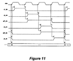
図4は、種々の実施形態による、高レベル概念を示す。システムクロック構成モジュール410は、システムクロックicd_sys_clkを生成する。システムクロックは、4相のtrc_q_clks信号、すなわち、trc_q1_clk、trc_q2_clk、trc_q3_clk、およびtrc_q4_clkを生成する、トレースQ−ジェネレータ420によって使用される。図11は、システムクロックclkinおよび命令の実行に関する関連直交信号の例示的タイミング図を示す。本実施形態では、clkinから派生した4つのクロックq1、q2、q3、q4が、1つの命令を実行するために使用される。トレースクロックは、内部クロックq1、q2、q3、q4から派生され得るか、または同じこれらのクロックであり得る。しかしながら、他の実施形態によると、異なる中央処理アーキテクチャが実装され、例えば、単一サイクルにおいて、命令を実行することを可能にし得る。
FIG. 4 illustrates a high level concept according to various embodiments. The system
図5は、トレースQ−ジェネレータ420の図の詳細を示す。これは、例えば、従来の様式において、4つのフリップフロップ510、520、530、および540によって形成される4ビット循環シフトレジスタであることができる。リセットソースのいくつかの実施例は、ウォッチドッグタイマWDTリセット、中央処理ユニットによって実行されるRESET命令、スタックオーバーフロー/アンダーフローリセット、およびマスタクリアMCLRリセットである。しかしながら、他のリセットソースおよび信号が、適用され得る。
FIG. 5 shows a diagram detail of the trace Q-
図4に戻ると、全体的リセットが生じると、リセットアナログユニット430は、一般的リセットが、システムクロック構成モジュール410を除き、チップ全体にアサートされることを可能にする。これは、システムクロックが、起動し続けることを可能にし、トレースQ−ジェネレータ420、したがって、また、トレースデータジェネレータ120も、動作を継続することができる。マイクロコントローラ中央処理ユニット110が、リセットに保持されている間、トレースデータジェネレータは、リセット関連トレース情報を記録し、次いで、トレースQ−ジェネレータに、記録が終了したことを通知する。
Returning to FIG. 4, when a general reset occurs, the
全体的リセット条件もまた、例えば、フリップフロップ450および460によって、それぞれ、trc_q2_clk信号およびtrc_q4_clk信号を使用して同期され、トレースQ−ジェネレータ420が停止すると、リセットアナログユニット430は、例えば、フリップフロップ480によって通知され、システムクロック構成モジュール430がリセットすることを可能にする。
The overall reset condition is also synchronized, for example, by flip-
リセットアナログユニット430の例示的実施形態は、図6に示される。リセットアナログユニット430は、システムクロック構成モジュール410が、そうするように通知された後、リセットすることを可能にする。システムクロック構成モジュール430がリセットすると同時に、ワンショットパルスtrc_reset_os1_pulseが、生成され、回路全体が、別のリセット発生検出のために再度備えていることができるように、シンクロナイザレジスタ要素450、460、480をリセットする。図6に示されるように、論理は、種々の制御信号を生成するために提供されることができる。他の論理回路も、デバイスの一般的設計に応じて、使用および適合されることができる。
An exemplary embodiment of the
このような種々の実施形態は、したがって、レベル高感度リセットおよびエッジ高感度リセットの両方に対処する能力を有し、リセットが生じるとすぐにマイクロコントローラシステム全体(システムクロック構成モジュールを除く)が、リセットすることを可能にし、したがって、命令トレースが進行中であってもネイティブ動作により近い。 Various such embodiments thus have the ability to handle both level sensitive and edge sensitive resets, and as soon as a reset occurs, the entire microcontroller system (except for the system clock configuration module) Allows resetting and is therefore closer to native operation even when instruction trace is in progress.
種々の実施形態は、モジュールが、チップリセットが生じるとすぐにリセットすることを防止された場合でも、システムクロック構成モジュールをリセットするために、最小パルス幅持続時間が保証されることを確実にする。 Various embodiments ensure that a minimum pulse width duration is guaranteed to reset the system clock configuration module, even if the module is prevented from resetting as soon as a chip reset occurs. .
以下のセクションは、デバイスと外部デバッグツールとの間のトレースデータインターフェースについて詳述する。例えば、図7に示されるようなトレースサブシステムは、デバッグツールによって捕捉および分析され得る、命令実行ストリームのリアルタイム記録を提供する。トレース動作は、デバッグツールが、ソースコードおよびプログラムメモリコンテンツへのアクセスを有し、CPU動作のいくつかの側面を推測することができると仮定する。 The following section details the trace data interface between the device and an external debug tool. For example, a trace subsystem as shown in FIG. 7 provides a real-time recording of instruction execution streams that can be captured and analyzed by a debug tool. The trace operation assumes that the debug tool has access to the source code and program memory content and can infer some aspect of CPU operation.
命令が、PCLに書き込むと(直接またはINDxを通してのいずれか)、新しいPCは、プログラムメモリ内の任意の場所にあり得る。この場合、命令パケットは、いわゆるフルプログラムカウンタ(FPC)パケットによって取って代わられる。FIFOは、図7に示されるように、コアデータレートをデバッグツールデータレート(TRSTALLによって統制される)と一致させるために使用されることができる。FIFOは、図7に図示されるように、CPUエンコーダから充填され、データエンコーダによって排出される。FIFOは、最大4096命令パケットを保持するが、有効動作サイズは、それぞれの制御ビットによって選択され得る。WATCHイベントパケットもまた、FIFO内に置かれ、したがって、処理中(in−flight)の命令パケットの実際の数は、通常、それより少ないであろう。TRCLK出力は、トグルすると、各クロックエッジに伴って、1データワードを出力する。出力クロックレートは、常時、CPU命令レートにリンクされ、ソフトウェアがSYSCLKを変更する場合、またはリセットがSYSCLKを変更する場合、変化するであろう。それぞれの構成によると、出力レートは、常時、命令期間あたり2つのトレースワードであることができる。レートは、命令あたり1および1/2まで減少されることができるが、これは、FIFOオーバーフローにつながる可能性が高くなるであろう。TRCLK出力は、データ変化に伴って、位相が一致するか、またはTRCPSビットの設定に応じて、位相がずれるかのいずれかとなるように選択されることができる。FIFO内エンコーディングは、ラインエンコーディングとは異なり、したがって、各FIFO場所は、TRDATインターフェースにおいて3データワードも表し得る。 When the instruction writes to the PCL (either directly or through INDx), the new PC can be anywhere in the program memory. In this case, the instruction packet is replaced by a so-called full program counter (FPC) packet. The FIFO can be used to match the core data rate with the debug tool data rate (controlled by TRSTALL), as shown in FIG. As shown in FIG. 7, the FIFO is filled from the CPU encoder and discharged by the data encoder. The FIFO holds a maximum of 4096 instruction packets, but the effective operation size can be selected by the respective control bits. WATCH event packets are also placed in the FIFO, so the actual number of in-flight instruction packets will usually be less. When the TRCLK output is toggled, it outputs one data word with each clock edge. The output clock rate is always linked to the CPU instruction rate and will change if software changes SYSCLK, or if reset changes SYSCLK. According to each configuration, the output rate can always be two trace words per instruction period. The rate can be reduced to 1 and 1/2 per instruction, but this will likely lead to a FIFO overflow. The TRCLK output can be selected to either coincide in phase with data changes or out of phase depending on the setting of the TRCPS bit. In-FIFO encoding is different from line encoding, so each FIFO location can also represent 3 data words in the TRDAT interface.
トレース機能停止機能が、実装されることができ、構成ビットが、TRSTALL入力が有効であるかどうか決定し得る。例えば、制御ビットTRXSE=1および信号TRSTALL=1であるとき、トレースFIFOは、ペイロード境界における排出を停止し、クロックを停止するであろう。TRSTALL(tr_stall_pin)が‘0’に戻ると、クロッキングは、再開し、FIFOは、データを再び排出し始めるであろう。トレースがイネーブルにされ、FIFOが空であるとき、IDLEまたはSLEEPパケットが、デバイスのスリープ状態に従って送信される。FIFOはまた、いくつかの実施形態によると、空にされることができ、トレースが、非アクティブ化されることができる。FIFOが満杯になる場合、システム応答は、それぞれの制御設定に依存し得る。いずれの場合も、オーバーフロー状態(機能停止される、またはデータをポストしない)は、それぞれの制御レジスタによって選択されるように、FIFOが25%または75%満杯のいずれかになるまで、持続するであろう。トレース実装に関する他の機能が、いくつかの実施形態によると、追加され得、説明されるようないくつかの機能は、実装されなくいこともある。典型的トレース信号タイミング図は、図8に示される。 A trace stop function can be implemented and the configuration bit can determine whether the TRSTALL input is valid. For example, when control bit TRXSE = 1 and signal TRSTALL = 1, the trace FIFO will stop draining at the payload boundary and stop the clock. When TRSTALL (tr_stal_pin) returns to '0', clocking will resume and the FIFO will begin draining data again. When tracing is enabled and the FIFO is empty, IDLE or SLEEP packets are sent according to the sleep state of the device. The FIFO can also be emptied and the trace can be deactivated according to some embodiments. If the FIFO is full, the system response may depend on the respective control settings. In either case, an overflow condition (decommissioned or not posting data) will persist until the FIFO is either 25% or 75% full, as selected by the respective control register. I will. Other functions related to trace implementation may be added according to some embodiments, and some functions as described may not be implemented. A typical trace signal timing diagram is shown in FIG.
トレースペイロードパケットは、CPUコアが実行する命令および選択されたデータイベントをエンコードし、また、トレースストリーム同期を提供する。ある実施形態によると、ほとんどのパケットは、1つまたは2つの7ビットワード、あるいはFPCパケットの場合、3ワードから成り得る。概して、パケットは、「ワード1」および随意の「ワード2」から成る。しかしながら、他の形式も、異なる実施形態に従って使用され得る。特定の実施形態によると、「ワード1」の値は、パケットを識別し、「ワード2」が存在するかどうかを暗示する。命令実行と同期するパケット(EX、EXD、およびRESET等)、およびWATCH、RESET、およびTRIGGERを含む非同期「イベント」パケットは、以下により詳細に説明される。
Trace payload packets encode instructions executed by the CPU core and selected data events, and also provide trace stream synchronization. According to certain embodiments, most packets may consist of one or two 7-bit words, or in the case of FPC packets, three words. Generally, a packet consists of “
同期パケットは、実行の順序で送られる。イベントパケットは、イベントとほぼ同時にストリーム中に現れるが、いくつかのイベントが同時に生じる場合、いくつかのレポートは、遅延されるであろう。ある場合には、FPCは、同期レポートであるが、他の場合には、イベントである。トランスポート層(TR)パケットRESYNC、IDLE、およびENDは、インターフェースデータストリームの種々の状態を管理および識別するために、要求に応じて挿入される。TRパケットRESYNCおよびIDLEは、命令トレースを分析すると破棄され得る。 Synchronization packets are sent in the order of execution. Event packets appear in the stream almost simultaneously with the event, but if several events occur simultaneously, some reports will be delayed. In some cases, the FPC is a synchronization report, but in other cases it is an event. Transport layer (TR) packets RESYNC, IDLE, and END are inserted on demand to manage and identify various states of the interface data stream. TR packets RESYNC and IDLE may be discarded when analyzing the instruction trace.
RESYNCパケットは、受信機が、正しく同期されていることを検証し得るように、それぞれの制御ビットによって規定されるように、周期的に挿入される。所定の時間間隔にほぼ対応する時に、他のFPCがその間隔内で送信されなかった場合のみ、FPCは、ストリームに追加されるであろう。これは、受信機が命令ストリームを正しく追跡していることのチェックを提供する。挿入されたFPCは、常時、追従する命令のアドレスを示す。パケット内のワード数は、パケットワード1の値によって決定される。RESYNCが、「ワード2」に対する正しくない値を伴うワード1として受信される場合、ストリームは、同期からずれ、エラーがフラグされるはずである。
The RESYNC packet is periodically inserted as defined by the respective control bits so that the receiver can verify that it is correctly synchronized. An FPC will be added to the stream only when no other FPC has been transmitted within that interval, almost corresponding to a given time interval. This provides a check that the receiver is tracking the instruction stream correctly. The inserted FPC always indicates the address of the instruction to be followed. The number of words in the packet is determined by the value of
表1は、2ワードパケットを伴う、最悪の場合の状況を図示し、2番目のワードは、0x7Dであり、その後に、RESYNCが続く。受信機が適切に同期されている場合、受信されたワード#3は、ワード1となり、ワード#4は、ワード2となり、パケット#2として示される完全なRESYNC対を形成するであろう。パケット#3は、ワード#5から開始し、正しく解釈されるであろう。
Table 1 illustrates the worst case situation with a two word packet, the second word is 0x7D, followed by RESYNC. If the receiver is properly synchronized, received word # 3 will be

表2は、第1のワードを複製し、受信機を同期から外す、クロックバウンスを伴う同一のデータを示す。ワード#1および#2は、データ=0x71(但し、これは、正しくない解釈である)を伴うEXDパケットとして受信され、ワード#3および#4は、RESYNC対として現れる。ワード#5は、新しいRESYNCパケットのワード1として見なされるが、ワード#6は、0x7Dではなく、同期から外れた状態を表す。ワード#6は、新しいパケットを開始する。
Table 2 shows the same data with clock bounce, duplicating the first word and taking the receiver out of sync.
トレースが開始する場合、またはデバッグ実行のために一時中断された後にトレースが再開する場合に送信される第1のパケットは、常時、FPCであろう。フルプログラムカウンタ(FPC)パケットは、ストリーム内に現れる次の命令の絶対アドレスをレポートする。FPCは、以下の状況においてレポートする。
−トレースの開始、
−オーバーフロー後の再開、および
−デバッグ後の再開、単に、次の命令のアドレスを示す。
The first packet sent when the trace starts or when the trace resumes after being suspended for debug execution will always be an FPC. A Full Program Counter (FPC) packet reports the absolute address of the next instruction that appears in the stream. The FPC reports in the following situations:
-Start of tracing,
-Resume after overflow, and-Resume after debugging, simply indicate the address of the next instruction.
FPCの全ての他の使用は、命令が実行され、ある場合には、その命令に対してレポートされたであろうパケットを置換することを示す。FPCが、分岐またはプログラムカウンタ変更命令の実行を表す場合、レポートされる値は、分岐標的アドレスである。FPCに続く命令パケットは、FPCが指し示す命令の実行を表す。 All other uses of FPC indicate that an instruction is executed and, in some cases, replaces a packet that would have been reported for that instruction. If the FPC represents execution of a branch or program counter change instruction, the reported value is the branch target address. The instruction packet following the FPC represents execution of the instruction indicated by the FPC.
GOTOおよびCALL命令は、プログラムカウンタPC[10:0]の最下位ビットが、デバッグ環境(アセンブリコード内)に対して既知であり、新しいPCの上位4ビットのみ、上位部分プログラムカウンタ(UPC)パケットにおいてレポートされると仮定する。しかしながら、他の実施形態は、より多いまたはより少ない情報をレポートし得る。レポートされる値は、0x0F&(PCLATH>>3)であることができ、PCLATHは、プログラムカウンタの上位ビットにラッチする、実装固有のレジスタを表す。相対分岐(BRA)の宛先は、ソースコードに既知であるので、命令は、単に、EXとしてレポートされる。種々のトレースペイロードが、実装され得る。表3は、異なるペイロード信号の例を示す。 For the GOTO and CALL instructions, the least significant bit of the program counter PC [10: 0] is known to the debug environment (in assembly code) and only the upper 4 bits of the new PC are the upper partial program counter (UPC) packet. Assume that However, other embodiments may report more or less information. The reported value can be 0x0F & (PCLATH >> 3), where PCLATH represents an implementation specific register that latches into the upper bits of the program counter. Since the destination of the relative branch (BRA) is known to the source code, the instruction is simply reported as EX. Various trace payloads can be implemented. Table 3 shows examples of different payload signals.
表4は、実際のトレース実施例を示す。 Table 4 shows actual trace examples.
トリガ入力の変化は、それぞれの制御ビットが設定されている場合、トレースパケットを生成するであろう。極性ビット=0である場合、イベントは、立ち上がりエッジでトリガするであろう。極性ビット=1である場合、イベントは、立ち下がりエッジでトリガするであろう。命令が、直接または間接的のいずれかにおいて、プログラムカウンタPCLに書き込むと、新しいPCは、プログラムメモリ内の任意の場所にあり得る。この場合、命令パケットは、FPCパケットによって置換される。 A change in trigger input will generate a trace packet if the respective control bit is set. If the polarity bit = 0, the event will trigger on the rising edge. If the polarity bit = 1, the event will trigger on the falling edge. When an instruction writes to the program counter PCL, either directly or indirectly, the new PC can be anywhere in the program memory. In this case, the instruction packet is replaced by the FPC packet.
FIFOは、コアデータレートをデバッグツールデータレート(TRSTALLによって統制される)と一致させるために使用される。FIFOは、図6によって図示されるように、CPUエンコーダから充填され、データエンコーダによって排出される。FIFOは、最大4096命令パケットを保持するが、有効動作サイズは、制御レジスタ内のそれぞれのビットによって選択される。WATCHイベントパケットもまた、FIFO内に置かれ、したがって、処理中の実際の命令パケットの数は、通常、より少ないであろう。 The FIFO is used to match the core data rate with the debug tool data rate (controlled by TRSTALL). The FIFO is filled from the CPU encoder and ejected by the data encoder, as illustrated by FIG. The FIFO holds a maximum of 4096 instruction packets, but the effective operation size is selected by each bit in the control register. WATCH event packets are also placed in the FIFO, so the actual number of instruction packets being processed will typically be less.
TRCLK出力は、トグルすると、各クロックエッジに伴って、1データワードを出力する。出力クロックレートは、常時、CPU命令レートにリンクされ、ソフトウェアがSYSCLKを変更する場合、またはリセットがSYSCLKを変更する場合、変化するであろう。関連付けられた制御レジスタ内のそれぞれのビットフィールドが設定されると、出力レートは、常時、命令期間あたり2トレースワードとなり得る。レートは、いくつかの実施形態によると、命令あたり1および1/2まで減少されることができるが、これは、FIFOオーバーフローにつながる可能性が高くなるであろう。トレースクロックTRCLK出力は、データ変化に伴って、位相が一致するか、またはTRCPS制御ビットの設定に応じて、位相がずれるかのいずれかとなるように選択されることができる。FIFO内エンコーディングは、ラインエンコーディングとは異なり、したがって、各FIFO場所は、TRDATインターフェースにおいて3データワードも表し得る。 When the TRCLK output is toggled, it outputs one data word with each clock edge. The output clock rate is always linked to the CPU instruction rate and will change if software changes SYSCLK, or if reset changes SYSCLK. As each bit field in the associated control register is set, the output rate can always be 2 trace words per instruction period. The rate can be reduced to 1 and 1/2 per instruction, according to some embodiments, but this will likely lead to a FIFO overflow. The trace clock TRCLK output can be selected to either coincide in phase with data changes, or out of phase depending on the setting of the TRCPS control bit. In-FIFO encoding is different from line encoding, so each FIFO location can also represent 3 data words in the TRDAT interface.
図9は、トレースサブシステム700の簡略化されたブロック図を示す。サブシステム700は、命令コードをコアおよびWATCHイベント信号から受信し、TRDAT信号上における配信のために、このデータをフォーマットする。シーケンスコントローラ710は、命令およびWATCHデータをFIFOにロードすることに関与する。各データパケットは、単一16−ビットワードとしてエンコードされる。q34の間、WATCH信号は、サンプリングされ、最高優先順位の信号が、エンコード、ロード、およびリセットされる。2つ以上の信号が、アサートされる場合、最高優先順位の信号のみ、ロードされ、他は、後続q34の機会を待たなければならない。レポート優先順位は、ブレークポイント番号に基づくので、イベントは、順序外でレポートされ得る。q12の間、以前の命令からのデータは、エンコードおよびロードされる(オプコードは、q3においてエンコードされ、バスデータは、安定しq3−q3、全て、立ち上がりq1において有効である)。概して、これは、命令期間毎に生じる。分岐および呼び出し命令ならびにインタラプトサイクルの場合、第1のサイクルの間、何もロードされず、パケットは、2回目のサイクルの間、エンコードされ(いわゆる「強制NOP」)、UPCおよびFPCが、正しいPC値とともに送られることを可能にする。その結果、2つのWATCHパケットが、分岐の間、ロードされ得る。SKIPおよびSTALLは、現在のコア動作に基づいてエンコードされる。
FIG. 9 shows a simplified block diagram of the
シーケンスコントローラ710は、命令サイクルあたり2回ロードすることができ、ストリームマネージャ730は、命令サイクルあたり2回アンロードすることができ、命令サイクルあたり最大4メモリサイクルを要求する。FIFOコントローラ720は、シーケンスコントローラ710によって提供されるデータを管理する。データは、ストリームマネージャ730によって要求されると、同一の順序で配信される。ストリームマネージャ730は、16−ビットFIFOワードをTRDAT信号で伝送されるデータワードに再フォーマットする。いくつかのパケット(例えば、EX)は、FIFOワード毎に単一TRDATワードをもたらす一方、他(例えば、FPC)は、より多くをもたらす。要求に応じて、トランスポート管理パケットRESYNC、IDLE、およびENDが、ストリーム内に挿入され、読み出し動作は、TRSTALL入力に従って中断される。2つのTRDATワードが、各命令サイクル期間の間に伝送される。TRCLK信号は、システムリセットの間、中断する(サイクルの一部を引き伸ばす)であろう(データは、損失されないであろう)。
The
図10は、トレース受信機として動作するデバッグツール820と連結される、種々の実施形態による、マイクロコントローラ810を伴うシステム800を示す。デバッグツールは、例えば、出願人によって製造された回路エミュレータ内のReal−ICEであることができる。受信機820は、トレース同期を行い、全IDLEおよびトランスポートパケットを破棄し、残りのパケットのバンドルを遠隔ホスト830、例えば、パケットストリーム解釈が行われる、パーソナルコンピュータまたはワークステーションに伝送する。
・ワード1分析−パケットを3ワード幅データバスに変換する。
・ダブレット(RESYNC、OVERFLOW等)を検証し、(a)ダブレットが連続ワード中にないとき、または(b)非実装ワード1コード値が認められるとき、同期エラーをフラグする。
・IDLEおよび他のトランスポートパケットを破棄し、残りの値をFIFOにスタックする。
・パケット全体を遠隔ホストに伝送する。
FIG. 10 illustrates a system 800 with a
Validate doublets (RESYNC, OVERFLOW, etc.) and flag synchronization errors when (a) doublets are not in consecutive words, or (b)
Discard IDLE and other transport packets and stack the remaining values in the FIFO.
• Transmit the entire packet to the remote host.
TRSTALLをアサートすると、受信機820は、最大もう6つのTRDATワード(2つの連続FPCパケットの均等物)に加え、再同期パイプラインの待ち行列に追加され得る2ワードを受け取る準備ができる。TRSTALLを解除すると、パケットワード1アラインメント(alignment)が、保証される。IDLEパケットのストリングから、大部分、または時として、全部が、破棄され、遠隔ホストに送られず、帯域幅を削減することができる。非実装オプコードおよびFPCワード3(7’h5x)もまた、同期エラーとしてフラグされ、1ワードパケットとして取り扱われるべきである。
When TRSTALL is asserted, the
FPCの3番目のワードは、単一ワードパケットのスタイルでエンコードされる(例えば、コード7’h5x)。同期しているかどうかにかかわらず、例えば、7’h5xの任意のワードに続くワードは、新しいパケットのワード1であると仮定され得る。ワード1を追跡する目的のために、OVERFLOW、RESYNC、SLEEP、およびENDパケットは、1ワードパケットとして取り扱われるべきである。7’h7Dが、1ワードパケットとして取り扱われるとき、別の7’h7D(対にされたRESYNCワード)である場合でも、続くパケットは、常時、ワード1値となるであろう。ワード1がアラインされた(aligned)(疑似)データは、ダブレット分析に通され、2つのRESYNCがストリーム内で連続的に現れないとき、同期失敗が認識される。同様に、OVERFLOW(7’h77)は、受信機が同期から外れているときに現れ得、2番目のワードが一致しない場合でも、正確に解釈されなければならない。これもまた、同期エラーをフラグし得る。受信機が、同期から外れている場合、1つのみの7’h7Cまたは7’h7Fが、最後に現れ得、第2の値を待つ間、ハングアップすることは受信機にとって好適ではないであろうため、同様の論法は、SLEEPおよびENDパケットにも適用されることができる。その一方で、3つの同じワードが、現れる場合もあり、これも受信機を混乱させるべきではない。
The third word of the FPC is encoded in the style of a single word packet (eg, code 7'h5x). Regardless of being synchronized, for example, the word following any word in 7'h5x may be assumed to be
完全分析のために、ホスト830は、トレースデータを、マイクロプロセッサをプログラムするために使用されたオリジナルソースコードと比較しなければならない。大部分の命令に対して、トレースデータは、実行が生じたことを示すが、動作詳細は、含まれない。分岐が、EXパケット(TRFPCB=0)のみをもたらすとき、分岐先は、ソースコードを検証することによってのみ決定されることができる。同様に、特定の実施形態によると、PCLATHへの書き込みは、部分的データのみを送り、評価を完了するために、ソース知識を要求する。動作に応じて、STALLパケットは、影響を受ける命令に先行するか、または続き得る。STALLパケットは、ユーザのディスプレイ上にハイライトされた表記によって、非典型的動作(例えば、不揮発性メモリへのファイル選択レジスタ(FSR)書き込み)が生じたことの示唆として見られ得る。WATCHレポートは、多くのパケットによって、トリガ命令を遅延させ得る。高密度に取り込まれたウォッチは、同一のウォッチが、読み出しが生じる前にトリガする場合、実際には損失され得る。ウォッチポイントは、データアドレスのみを識別するので、トレース分析は、直接アドレスモード(BSRおよびオプコードの知識を要求する)から、または間接モード(FSRの知識を要求する)からかにかかわらず、データアクセスポインタ値を再構成することができなければならない。ウォッチデータは、常時、ウォッチイベントの最新の発生に由来する。いくつかのFPCパケットは、命令が実行された(例えば、RETURN命令)ことを暗示するが、他のインスタンスは、単なる参考情報であることに留意されたい。
For complete analysis, the
図12は、開発プログラムを起動し、例えば、USBインターフェースを介して、外部デバッガ/プログラミングユニット520と接続される、パーソナルコンピュータ等のホストを伴う、典型的デバッグ/プログラミングシステム500を示す。外部デバッガプログラミングユニット520は、デバッガ/プログラマ520内で生成された電源電圧を供給し得る専用インターフェースを提供する。しかしながら、他の実施形態は、専用電源を介して供給電圧を供給し得、標的システムは、自己給電され得る。実際のデバッグ/プログラミングインターフェースは、デバッガ/プログラミングユニット520によって提供される単方向性クロック信号ICDCLKおよび双方向性データラインICDDataを伴う、同期シリアルインターフェースによって提供され得る。したがって、最低限でも、3つの接続ライン、ICDCLK、ICDData、および基準電位(GND)が、デバッガ/プログラミングユニット520と、最低限として、前述のように、種々の実施形態による、デバッグ/プログラミングインターフェースを伴うマイクロコントローラであり得る、標的システム510を連結するために使用され得る。
FIG. 12 shows an exemplary debug /
そのようなシステムは、ユーザが、ホスト上で起動するデバッグプログラムを、プログラムがリアルタイムで実行している間、前述されたような条件を有する種々のブレークポイントを設定し、随意に、追加の接続ラインを通して、トレース情報を受信するようにプログラムすることを可能にする。デバッグソフトウェアは、ソースコード内のその位置に関して、種々のブレークポイントを追跡する間、デバッガ/プログラマ520は、それぞれのブレークポイントを設定し、その関連付けられたレジスタを構成する標的デバイスに、ブレークポイント情報を通信する。また、トレース能力の設定および構成は、デバッガ/プログラマ520によって、標的デバイス510に通信される。例えば、メモリ内に記憶されたデータ値の一致によってトリガされる特定のブレークポイントが、設定され得る。ユーザは、次いで、ホストPC530上で起動するデバッガソフトウェアを通して、標的デバイス510のソフトウェアの実行を開始する。標的ソフトウェアの実行は、ブレークポイントが検出されるときのみ停止される。しかしながら、トレース情報は、標的プログラムの実行の間、継続して自動転送され得る。ホストコンピュータ530は、このトレースデータを評価し、テキスト形態において、またはグラフィカルディスプレイを使用してのいずれかにおいて、それを利用可能にする。前述のように、リセットイベントはまた、種々の実施形態によると、トレースサブシステムが、依然として、クロックされているため、完全にトレースされることができる。
Such a system allows the user to set various breakpoints with conditions as described above and optionally additional connections while the program is running in real time on the host. Allows programming to receive trace information through a line. While the debug software tracks various breakpoints with respect to their location in the source code, the debugger /
本実施形態は、前述のような特徴を実装することによって、トレースストリームのより優れた分析を可能にする。種々の実施形態は、したがって、オンチップデバッグ能力水準を高め、高度デバッグ能力を多くの異なるユーザにもたらすことを可能にするであろう。 This embodiment allows for better analysis of the trace stream by implementing features such as those described above. Various embodiments will therefore increase the on-chip debugging capability level and allow advanced debugging capabilities to be brought to many different users.
Claims (20)
中央処理ユニットと、
トレースモジュールを含むデバッグ回路と、
内部クロック信号を提供するためのシステムクロックモジュールであって、処理デバイスをリセットすることは、前記システムクロックモジュールが最小リセット期間中にリセットされることを要求する、システムクロックモジュールと、
デバッグモードの間、前記システムクロックモジュールがリセット信号を受信することを防止するリセット検出ユニットと
を備え、
前記トレースモジュールは、リセット信号が検出された後、トレース情報を記録するように動作可能であり、前記トレース情報を記録した後、前記システムクロックモジュールをリセットする、前記最小リセット期間を有する信号を生成する、プロセッサデバイス。 A processor device having debugging capability, the processor device comprising:
A central processing unit;
A debug circuit including a trace module ;
A system clock module for providing an internal clock signal, wherein resetting a processing device requires the system clock module to be reset during a minimum reset period; and
A reset detection unit that prevents the system clock module from receiving a reset signal during debug mode, and
The trace module is operable to record trace information after a reset signal is detected, and generates a signal having the minimum reset period that resets the system clock module after recording the trace information To the processor device.
中央処理ユニット(CPU)によってコードを実行することと、
リセットの決定に応じて、前記システムクロックモジュールを除く、マイクロコントローラの内部ユニットにリセット信号を自動転送することにより、トレースモジュールのさらなる動作を可能にすることと、
前記トレースモジュールによって、前記リセットの受信後、トレース情報を記録することと、
前記トレース情報を記録した後、前記システムクロックモジュールをリセットする、前記最小リセット期間を有する信号を生成することと
を含む、方法。 A method of debugging code executed in a processor device comprising a system clock module for providing an internal clock signal, wherein resetting a processing device causes the system clock module to be reset during a minimum reset period It requires that, the method comprising:
Executing code by a central processing unit (CPU);
Allowing further operation of the trace module by automatically transferring a reset signal to an internal unit of the microcontroller, excluding the system clock module, in response to a reset decision;
Recording trace information after receiving the reset by the trace module;
Generating the signal having the minimum reset period to reset the system clock module after recording the trace information.
Applications Claiming Priority (3)
| Application Number | Priority Date | Filing Date | Title |
|---|---|---|---|
| US201261643725P | 2012-05-07 | 2012-05-07 | |
| US61/643,725 | 2012-05-07 | ||
| PCT/US2013/039934 WO2013169766A1 (en) | 2012-05-07 | 2013-05-07 | Processor device with reset condition trace capabilities |
Publications (3)
| Publication Number | Publication Date |
|---|---|
| JP2015516637A JP2015516637A (en) | 2015-06-11 |
| JP2015516637A5 JP2015516637A5 (en) | 2016-06-30 |
| JP6220863B2 true JP6220863B2 (en) | 2017-10-25 |
Family
ID=48570432
Family Applications (1)
| Application Number | Title | Priority Date | Filing Date |
|---|---|---|---|
| JP2015511620A Active JP6220863B2 (en) | 2012-05-07 | 2013-05-07 | Processor device with reset condition trace capability |
Country Status (6)
| Country | Link |
|---|---|
| US (1) | US9298570B2 (en) |
| EP (1) | EP2847682B1 (en) |
| JP (1) | JP6220863B2 (en) |
| KR (1) | KR20150008441A (en) |
| CN (1) | CN104380266B (en) |
| WO (1) | WO2013169766A1 (en) |
Families Citing this family (11)
| Publication number | Priority date | Publication date | Assignee | Title |
|---|---|---|---|---|
| US20150019775A1 (en) * | 2013-03-14 | 2015-01-15 | Microchip Technology Incorporated | Single Wire Programming and Debugging Interface |
| US20160103722A1 (en) * | 2014-10-10 | 2016-04-14 | Qualcomm Incorporated | Hardware lockup detection mechanism for user devices |
| US9690727B2 (en) * | 2014-10-31 | 2017-06-27 | Atmel Corporation | System internal latency measurements in realtime applications |
| US10534688B2 (en) * | 2016-09-30 | 2020-01-14 | Intel Corporation | Trace hub logic with automatic event triggering |
| US10754759B1 (en) * | 2018-02-05 | 2020-08-25 | Xilinx, Inc. | Breakpointing circuitry that evaluates breakpoint conditions while running clock to target circuit |
| US20190370016A1 (en) * | 2018-05-31 | 2019-12-05 | Hamilton Sundstrand Corporation | Auto detection of jtag debuggers/emulators |
| CN109117362B (en) * | 2018-06-26 | 2020-08-25 | 华东师范大学 | PLC program verification system based on intermediate language |
| EP3661056B1 (en) * | 2018-11-27 | 2022-05-25 | STMicroelectronics Application GmbH | Processing system, related integrated circuit, device and method |
| CN110032482A (en) * | 2019-04-11 | 2019-07-19 | 盛科网络(苏州)有限公司 | Sheet sand covered device and method |
| DE112020006396T5 (en) * | 2020-02-27 | 2022-10-13 | Microchip Technology Incorporated | SYNCHRONIZING SEQUENCE NUMBERS IN A NETWORK |
| US11442805B1 (en) * | 2021-03-03 | 2022-09-13 | Siliconch Systems Pvt Ltd | System and method for debugging microcontroller using low-bandwidth real-time trace |
Family Cites Families (12)
| Publication number | Priority date | Publication date | Assignee | Title |
|---|---|---|---|---|
| JPH0736735A (en) * | 1993-07-22 | 1995-02-07 | Agency Of Ind Science & Technol | Debugging device |
| KR100255026B1 (en) * | 1994-12-28 | 2000-05-01 | 디. 크레이그 노룬드 | Microprocessor and debug system |
| US5825706A (en) * | 1997-10-27 | 1998-10-20 | Motorola, Inc. | Circuit and method for retaining data in DRAM in a portable electronic device |
| US6792527B1 (en) * | 2000-12-22 | 2004-09-14 | Xilinx, Inc. | Method to provide hierarchical reset capabilities for a configurable system on a chip |
| US7051197B2 (en) * | 2002-11-22 | 2006-05-23 | Texas Instruments Incorporated | Tracing through reset |
| US7237151B2 (en) * | 2002-12-17 | 2007-06-26 | Texas Instruments Incorporated | Apparatus and method for trace stream identification of a processor reset |
| JP2006011991A (en) * | 2004-06-29 | 2006-01-12 | Meidensha Corp | Computer controller and software execution recording mode therefor |
| CN100401267C (en) * | 2006-09-01 | 2008-07-09 | 上海大学 | Chip dynamic tracing method of microprocessor |
| JP2008129669A (en) * | 2006-11-17 | 2008-06-05 | Meidensha Corp | Hardware failure recording device and method |
| JP2008276324A (en) * | 2007-04-25 | 2008-11-13 | Kyocera Mita Corp | Reset device, and image forming apparatus having reset device |
| US7681078B2 (en) * | 2007-05-18 | 2010-03-16 | Freescale Semiconductor, Inc. | Debugging a processor through a reset event |
| JP5533097B2 (en) * | 2010-03-18 | 2014-06-25 | 株式会社リコー | Information processing apparatus, image forming apparatus, and information processing program |
-
2013
- 2013-05-07 CN CN201380031912.9A patent/CN104380266B/en active Active
- 2013-05-07 EP EP13726614.4A patent/EP2847682B1/en active Active
- 2013-05-07 KR KR20147033969A patent/KR20150008441A/en active IP Right Grant
- 2013-05-07 US US13/888,367 patent/US9298570B2/en active Active
- 2013-05-07 JP JP2015511620A patent/JP6220863B2/en active Active
- 2013-05-07 WO PCT/US2013/039934 patent/WO2013169766A1/en active Application Filing
Also Published As
| Publication number | Publication date |
|---|---|
| EP2847682A1 (en) | 2015-03-18 |
| WO2013169766A1 (en) | 2013-11-14 |
| KR20150008441A (en) | 2015-01-22 |
| EP2847682B1 (en) | 2019-07-03 |
| US20130297974A1 (en) | 2013-11-07 |
| CN104380266B (en) | 2017-07-18 |
| CN104380266A (en) | 2015-02-25 |
| JP2015516637A (en) | 2015-06-11 |
| US9298570B2 (en) | 2016-03-29 |
Similar Documents
| Publication | Publication Date | Title |
|---|---|---|
| JP6220863B2 (en) | Processor device with reset condition trace capability | |
| JP6397815B2 (en) | Processor device with instruction trace capability | |
| KR101430218B1 (en) | Debug state machine and processor including the same | |
| US9830241B2 (en) | Debug in a multicore architecture | |
| EP1805621B1 (en) | Method and system for debugging a multi-threaded program executing in a multicore architecture | |
| JP6116670B2 (en) | Devices with configurable breakpoints based on interrupt status | |
| US20060267818A1 (en) | Saving Resources by Deducing the Total Prediction Events | |
| US7721263B2 (en) | Debug event instruction | |
| US8706937B2 (en) | Method and system of debugging multicore bus transaction problems | |
| US20060255976A1 (en) | Distributed Depth Trace Receiver | |
| US20060255978A1 (en) | Enabling Trace and Event Selection Procedures Independent of the Processor and Memory Variations | |
| US20060279443A1 (en) | Trading Off Visibility for Volume of Data When Profiling Memory Events | |
| US7590893B2 (en) | Recording control point in trace receivers | |
| US7676697B2 (en) | Using a delay line to cancel clock insertion delays | |
| US7613951B2 (en) | Scaled time trace | |
| Matraszek et al. | FrankenTrace: Low-Cost, Cycle-Level, Widely Applicable Program Execution Tracing for ARM Cortex-M SoC |
Legal Events
| Date | Code | Title | Description |
|---|---|---|---|
| A521 | Request for written amendment filed |
Free format text: JAPANESE INTERMEDIATE CODE: A523 Effective date: 20160506 |
|
| A621 | Written request for application examination |
Free format text: JAPANESE INTERMEDIATE CODE: A621 Effective date: 20160506 |
|
| A977 | Report on retrieval |
Free format text: JAPANESE INTERMEDIATE CODE: A971007 Effective date: 20170307 |
|
| A131 | Notification of reasons for refusal |
Free format text: JAPANESE INTERMEDIATE CODE: A131 Effective date: 20170310 |
|
| A521 | Request for written amendment filed |
Free format text: JAPANESE INTERMEDIATE CODE: A523 Effective date: 20170602 |
|
| TRDD | Decision of grant or rejection written | ||
| A01 | Written decision to grant a patent or to grant a registration (utility model) |
Free format text: JAPANESE INTERMEDIATE CODE: A01 Effective date: 20170904 |
|
| A61 | First payment of annual fees (during grant procedure) |
Free format text: JAPANESE INTERMEDIATE CODE: A61 Effective date: 20171002 |
|
| R150 | Certificate of patent or registration of utility model |
Ref document number: 6220863 Country of ref document: JP Free format text: JAPANESE INTERMEDIATE CODE: R150 |
|
| R250 | Receipt of annual fees |
Free format text: JAPANESE INTERMEDIATE CODE: R250 |
|
| R250 | Receipt of annual fees |
Free format text: JAPANESE INTERMEDIATE CODE: R250 |
|
| R250 | Receipt of annual fees |
Free format text: JAPANESE INTERMEDIATE CODE: R250 |
|
| R250 | Receipt of annual fees |
Free format text: JAPANESE INTERMEDIATE CODE: R250 |