KR20150002000A - Semiconductor device and operation method thereof - Google Patents
Semiconductor device and operation method thereof Download PDFInfo
- Publication number
- KR20150002000A KR20150002000A KR20130075218A KR20130075218A KR20150002000A KR 20150002000 A KR20150002000 A KR 20150002000A KR 20130075218 A KR20130075218 A KR 20130075218A KR 20130075218 A KR20130075218 A KR 20130075218A KR 20150002000 A KR20150002000 A KR 20150002000A
- Authority
- KR
- South Korea
- Prior art keywords
- voltage
- lines
- source
- memory cells
- erase
- Prior art date
Links
Images


Classifications
-
- G—PHYSICS
- G11—INFORMATION STORAGE
- G11C—STATIC STORES
- G11C16/00—Erasable programmable read-only memories
- G11C16/02—Erasable programmable read-only memories electrically programmable
- G11C16/06—Auxiliary circuits, e.g. for writing into memory
- G11C16/08—Address circuits; Decoders; Word-line control circuits
-
- G—PHYSICS
- G11—INFORMATION STORAGE
- G11C—STATIC STORES
- G11C16/00—Erasable programmable read-only memories
- G11C16/02—Erasable programmable read-only memories electrically programmable
- G11C16/06—Auxiliary circuits, e.g. for writing into memory
- G11C16/34—Determination of programming status, e.g. threshold voltage, overprogramming or underprogramming, retention
- G11C16/3418—Disturbance prevention or evaluation; Refreshing of disturbed memory data
- G11C16/3427—Circuits or methods to prevent or reduce disturbance of the state of a memory cell when neighbouring cells are read or written
-
- G—PHYSICS
- G11—INFORMATION STORAGE
- G11C—STATIC STORES
- G11C16/00—Erasable programmable read-only memories
- G11C16/02—Erasable programmable read-only memories electrically programmable
- G11C16/04—Erasable programmable read-only memories electrically programmable using variable threshold transistors, e.g. FAMOS
- G11C16/0483—Erasable programmable read-only memories electrically programmable using variable threshold transistors, e.g. FAMOS comprising cells having several storage transistors connected in series
-
- G—PHYSICS
- G11—INFORMATION STORAGE
- G11C—STATIC STORES
- G11C16/00—Erasable programmable read-only memories
- G11C16/02—Erasable programmable read-only memories electrically programmable
- G11C16/06—Auxiliary circuits, e.g. for writing into memory
-
- G—PHYSICS
- G11—INFORMATION STORAGE
- G11C—STATIC STORES
- G11C16/00—Erasable programmable read-only memories
- G11C16/02—Erasable programmable read-only memories electrically programmable
- G11C16/06—Auxiliary circuits, e.g. for writing into memory
- G11C16/34—Determination of programming status, e.g. threshold voltage, overprogramming or underprogramming, retention
- G11C16/3436—Arrangements for verifying correct programming or erasure
- G11C16/344—Arrangements for verifying correct erasure or for detecting overerased cells
- G11C16/3445—Circuits or methods to verify correct erasure of nonvolatile memory cells
Abstract
Description
본 발명은 반도체 장치 및 이의 동작 방법에 관한 것으로, 보다 구체적으로는 수직채널을 갖는 반도체 장치 및 이의 동작 방법에 관한 것입니다.
The present invention relates to a semiconductor device and a method of operating the same, and more particularly, to a semiconductor device having a vertical channel and a method of operating the semiconductor device.
휴대전화, 이동식 메모리 장치 및 디지털 카메라의 수요가 증가하면서, 이러한 제품들의 메모리 장치로 주로 사용되고 있는 불휘발성 메모리 장치의 수요도 증가하고 있다. 불휘발성 메모리 장치 중에서도 낸드 플래시 메모리 장치(NAND flash memory device)가 데이터 저장 장치로 많이 사용되고 있다. As the demand for mobile phones, mobile memory devices and digital cameras increases, the demand for nonvolatile memory devices, which are mainly used as memory devices for these products, is also increasing. Of the nonvolatile memory devices, NAND flash memory devices are widely used as data storage devices.
낸드 플래시 메모리 장치는 셀 스트링이 반도체 기판에 수평하게 형성된 2차원 반도체 장치와, 셀 스트링이 반도체 기판에 수직으로 형성된 3차원 반도체 장치로 구분될 수 있다. A NAND flash memory device can be classified into a two-dimensional semiconductor device in which a cell string is formed horizontally on a semiconductor substrate and a three-dimensional semiconductor device in which a cell string is formed perpendicularly to the semiconductor substrate.
3차원 반도체 장치는 2차원 반도체 장치의 집적도 한계를 해소하기 위하여 고안된 메모리 장치로써, 반도체 기판 상에 수직으로 형성된 다수의 셀 스트링들을 포함한다. 셀 스트링들은 비트라인과 소오스라인 사이에 직렬로 연결된 드레인 셀렉트 트랜지스터, 메모리 셀들 및 소오스 셀렉트 트랜지스터를 포함한다. A three-dimensional semiconductor device is a memory device designed to overcome the limit of integration of a two-dimensional semiconductor device, and includes a plurality of cell strings formed vertically on a semiconductor substrate. The cell strings include a drain select transistor, memory cells, and a source select transistor connected in series between the bit line and the source line.
한편, 3차원 반도체 장치의 드레인 셀렉트 트랜지스터 부근에 연결된 메모리 셀들은 소오스라인 부근의 저항으로 인하여 프로그램 및 리드 동작시 메모리 셀들의 문턱전압이 변경될 수 있는데, 이로 인하여 3차원 반도체 장치의 신뢰도가 저하될 수 있다.On the other hand, in the memory cells connected to the drain select transistor of the three-dimensional semiconductor device, the threshold voltage of the memory cells can be changed during the program and read operations due to the resistance in the vicinity of the source line, .
본 발명의 실시예는 프로그램, 리드 및 소거 동작의 신뢰도를 개선할 수 있는 반도체 장치 및 이의 동작 방법을 제공한다.
Embodiments of the present invention provide a semiconductor device and an operation method thereof capable of improving the reliability of a program, a read, and an erase operation.
본 발명에 따른 반도체 장치는 반도체 기판에 수직한 다수의 셀 스트링들을 포함하며, 상기 셀 스트링들에 연결된 다수의 비트라인들 및 소오스라인들을 서로 공유하고 워드라인들이 각각 연결된 다수의 메모리 블록들과, 프로그램 동작에 필요한 데이터를 저장하고, 상기 프로그램 동작과 리드 동작 및 소거 동작 수행시 검증동작을 수행하도록 구성된 페이지 버퍼들과, 상기 프로그램, 리드 및 소거 동작 수행시 상기 페이지 버퍼에 저장된 상기 데이터에 해당되는 전압 및 외부로부터 공급받은 다양한 전압들을 상기 비트라인들 및 상기 소오스라인들에 선택적으로 전달하도록 구성된 선택 스위치부 및 상기 페이지 버퍼들 및 상기 선택 스위치부를 제어하도록 구성된 제어회로를 포함한다. A semiconductor device according to the present invention includes a plurality of cell blocks each including a plurality of cell strings perpendicular to a semiconductor substrate, a plurality of bit lines and source lines connected to the cell strings, A page buffer configured to store data necessary for a program operation and perform a verify operation when performing the program operation and the read operation and the erase operation; And a control circuit configured to selectively control the page buffers and the selection switch unit to selectively transmit a voltage and various voltages supplied from the outside to the bit lines and the source lines.
본 발명에 따른 반도체 장치의 동작방법은, 소오스라인들과 비트라인들 사이에 연결되고 반도체 기판 상에 수직하게 배열된 다수의 셀 스트링들을 포함하는 메모리 블록의 프로그램 방법에 있어서, 상기 소오스라인들에 인접한 메모리 셀들부터 제1 메모리 셀들까지 순차적으로 프로그램 동작을 수행하는 단계 및 상기 비트라인들에 인접한 메모리 셀들부터 제2 메모리 셀들까지 순차적으로 프로그램 동작을 수행하는 단계를 포함한다. A method of operating a semiconductor device according to the present invention is a method of programming a memory block including a plurality of cell strings connected between source lines and bit lines and vertically arranged on a semiconductor substrate, Sequentially performing a program operation from adjacent memory cells to the first memory cells, and sequentially performing programming operations from the memory cells adjacent to the bit lines to the second memory cells.
본 발명에 따른 반도체 장치의 동작방법은, 소오스라인들과 비트라인들 사이에 연결되고 반도체 기판 상에 수직하게 배열된 다수의 셀 스트링들을 포함하는 메모리 블록의 리드 방법에 있어서, 상기 소오스라인들에 인접한 메모리 셀들부터 제1 메모리 셀들까지 순차적으로 리드 동작을 수행하는 단계 및 상기 비트라인들에 인접한 메모리 셀들부터 제2 메모리 셀들까지 순차적으로 리드 동작을 수행하는 단계를 포함한다. A method of operating a semiconductor device according to the present invention is a method of reading a memory block including a plurality of cell strings connected between source lines and bit lines and vertically arranged on a semiconductor substrate, Sequentially performing a read operation from adjacent memory cells to the first memory cells, and sequentially performing a read operation from the memory cells adjacent to the bit lines to the second memory cells.
본 발명에 따른 반도체 장치의 동작방법은, 소오스라인들과 비트라인들 사이에 연결되고 반도체 기판 상에 수직하게 배열된 다수의 셀 스트링들을 포함하는 메모리 블록의 소거 방법에 있어서, 선택된 메모리 블록에 연결된 비트라인들 및 소오스라인들에 소거전압을 인가하고, 상기 선택된 메모리 블록에 연결된 워드라인들에 소거 허용전압을 인가하여 선택된 메모리 블록에 포함된 메모리 셀들을 소거하도록 소거 동작을 수행하는 단계, 상기 메모리 셀들에 대한 소거 검증동작을 수행하는 단계 및 상기 비트라인들 및 상기 소오스라인들 중 소거 완료된 셀 스트링들에 연결된 비트라인들 및 소오스라인들에 소거 억제 전압을 인가하는 단계를 포함한다.
A method of operating a semiconductor device according to the present invention is a method for erasing a memory block including a plurality of cell strings connected between source lines and bit lines and vertically arranged on a semiconductor substrate, Applying an erase voltage to bit lines and source lines and applying an erase allowable voltage to word lines connected to the selected memory block to perform an erase operation to erase memory cells included in the selected memory block, Performing an erase verify operation on the cells and applying an erase suppression voltage to bit lines and source lines connected to the erased cell strings of the bit lines and the source lines.
본 기술은 3차원 반도체 장치의 동작시 셀 스트링들 저항을 감소시킴으로써, 프로그램 동작시 디스터브를 억제하고 리텐션 특성을 개선할 수 있고, 리드 동작의 신뢰도를 개선할 수 있으며, 소거 동작시 메모리 셀들의 문턱전압 분포 폭이 증가하는 것을 억제하면서 소거 스트레스를 감소시킬 수 있다.
By reducing the resistance of the cell strings in operation of the three-dimensional semiconductor device, the present technology can suppress disturbance and improve retention characteristics during program operation, improve the reliability of the read operation, The erasing stress can be reduced while suppressing an increase in the threshold voltage distribution width.
도 1은 본 발명에 따른 반도체 장치를 개략적으로 설명하기 위한 블록도이다.
도 2는 본 발명의 제1 실시예에 따른 메모리 블록들의 구성을 설명하기 위한 도면이다.
도 3은 도 2에 도시된 메모리 블록을 구체적으로 설명하기 위한 회로도이다.
도 4는 도 3에 도시된 셀 스트링 그룹과 페이지 버퍼 간의 연결관계와 제1 실시예에 따른 프로그램 및 독출 동작을 설명하기 위한 회로도이다.
도 5 및 도 6은 제1 실시예에 따른 메모리 블록들의 소거 동작을 설명하기 위한 도면이다.
도 7은 본 발명의 제2 실시예에 따른 메모리 블록들의 구성을 설명하기 위한 도면이다.
도 8은 도 7에 도시된 메모리 블록들을 구체적으로 설명하고, 제2 실시예에 따른 프로그램, 독출 및 소거 동작을 설명하기 위한 도면이다.1 is a block diagram schematically illustrating a semiconductor device according to the present invention.
2 is a diagram for explaining a configuration of memory blocks according to a first embodiment of the present invention.
3 is a circuit diagram for specifically explaining the memory block shown in FIG.
FIG. 4 is a circuit diagram for explaining the connection relationship between the cell string group and the page buffer shown in FIG. 3 and the program and read operation according to the first embodiment.
5 and 6 are diagrams for explaining the erase operation of the memory blocks according to the first embodiment.
7 is a view for explaining a configuration of memory blocks according to a second embodiment of the present invention.
8 is a diagram for describing the memory blocks shown in FIG. 7 in detail and explaining the program, read and erase operations according to the second embodiment.
이하, 첨부된 도면을 참조하여 본 발명의 바람직한 실시 예를 설명하기로 한다. 그러나, 본 발명은 이하에서 개시되는 실시 예에 한정되는 것이 아니라 서로 다른 다양한 형태로 구현될 수 있으며, 단지 본 실시 예는 본 발명의 개시가 완전하도록 하며 통상의 지식을 가진자에게 발명의 범주를 완전하게 알려주기 위해 제공되는 것이다.
Hereinafter, preferred embodiments of the present invention will be described with reference to the accompanying drawings. It should be understood, however, that the invention is not limited to the disclosed embodiments, but may be embodied in many different forms and should not be construed as limiting the scope of the invention to those skilled in the art It is provided to let you know completely.
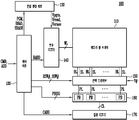
도 1은 본 발명에 따른 반도체 장치를 개략적으로 설명하기 위한 블록도이다. 1 is a block diagram schematically illustrating a semiconductor device according to the present invention.
도 1을 참조하면, 반도체 장치(100)는 3차원 구조로 이루어진 메모리 셀 어레이(110), 메모리 셀 어레이(110)에 포함된 메모리 셀들을 프로그램, 독출 및 소거하도록 구성된 주변회로들(130~170) 및 주변회로들(130~170)을 제어하도록 구성된 제어회로(120)를 포함한다. 1, a
메모리 셀 어레이(110)는 다수의 메모리 블록들을 포함하며, 각각의 메모리 블록은 수직채널을 갖는 다수의 셀 스트링들을 포함하며, 각각의 셀 스트링들은 수직채널을 따라 서로 직렬로 연결된 다수의 메모리 셀들을 포함한다. The
주변회로들(130~170)은 전압 생성 회로(130), 로우 디코더(140), 선택 스위치부(150), 페이지 버퍼부(160) 및 컬럼 디코더(170)를 포함한다. The
전압 생성 회로(130)는 프로그램 신호(PGM), 독출 신호(READ) 또는 소거 신호(ERASE)에 응답하여 각 동작에 필요한 동작 전압들, 예를 들면 프로그램 전압(Vpgm), 독출 전압(Vread) 또는 소거전압(Verasese)을 생성한다. 도면에는 도시되지 않았으나, 전압 생성 회로(130)는 프로그램 전압(Vpgm), 독출 전압(Vread) 및 소거전압(Verase) 외에도 다양한 레벨의 전압들을 생성한다. The
로우 디코더(140)는 로우 어드레스(RADD)에 응답하여 메모리 블록을 선택하고, 전압 생성 회로(130)에서 생성된 동작 전압들을 선택된 메모리 블록의 워드라인들(WL) 및 셀렉트 라인들(미도시)에 전달한다. The
선택 스위치부(150)는 외부의 전압원들로부터 다양한 전압들(V#)을 공급받고, 비트라인 선택 신호들(BSW#) 및 소오스라인 선택 신호들(SSW#)에 응답하여 전압들(V#)을 비트라인들(BL) 또는 소오스라인들(SL)에 전달하거나, 페이지 버퍼부(160)의 페이지 라인들(PL)을 통해 전달된 전압을 비트라인들(BL) 또는 소오스라인들(SL)에 전달한다. The
페이지 버퍼부(160)는 다수의 페이지 버퍼들(PB)을 포함한다. 페이지 버퍼들(PB)은 페이지 버퍼 제어신호(PBSIG)에 응답하여 프로그램 동작에 필요한 데이터를 저장하거나, 프로그램, 리드 및 소거 동작시 검증 동작을 수행하도록 구성된다. 페이지 버퍼들(PB)은 저장된 데이터에 해당되는 전압을 페이지 라인들(PL)에 전달하거나, 페이지 라인들(PL)에 인가된 전압을 센싱한다. The
컬럼 디코더(170)는 컬럼 어드레스(CADD)에 응답하여 페이지 버퍼들(PB)에 데이터를 전달하거나, 페이지 버퍼들(PB)로부터 데이터를 전달받는다. The
제어회로(120)는 명령신호(CMD) 및 어드레스(ADD)에 응답하여 프로그램 신호(PGM), 독출 신호(READ) 또는 소거 신호(ERASE)를 출력하고, 로우 어드레스(RADD) 및 컬럼 어드레스(CADD)를 출력하고, 페이지 버퍼 신호(PBSIG)를 출력한다.
The
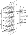
도 2는 본 발명의 제1 실시예에 따른 메모리 블록들의 구성을 설명하기 위한 도면이다. 2 is a diagram for explaining a configuration of memory blocks according to a first embodiment of the present invention.
도 2를 참조하면, 메모리 셀 어레이(110)는 다수의 메모리 블록들(BLK1~BLKm; m은 양의 정수)을 포함한다. 제1 실시예에서는 메모리 블록들(BLK1~BLKm)이 단층으로 이루어진다. 각각의 메모리 블록들(BLK1~BLKm)은 다수의 비트라인들(... BLn-1, BL, BLn+1, ...) 및 다수의 소오스라인들(... SLn-1, SL, SLn+1, ...)을 공유하며, 워드라인들(WL)이 각각 연결된다. 즉, 메모리 블록들(BLK1~BLKm)에는 다수의 셀 스트링들(도시되지 않음)이 포함되는데, 동일한 메모리 블록 내에 포함된 다수의 셀 스트링들은 서로 다른 비트라인들(... BLn-1, BL, BLn+1, ...) 및 소오스라인들(... SLn-1, SL, SLn+1, ...)에 연결되며, 워드라인들(WL)을 공유한다. 또한, 서로 다른 메모리 블록들에 포함된 셀 스트링들은 비트라인들(... BLn-1, BL, BLn+1, ...) 및 소오스라인들(... SLn-1, SL, SLn+1, ...)을 공유하지만, 워드라인들(WL)은 공유하지 않는다.
Referring to FIG. 2, the
도 3은 도 2에 도시된 메모리 블록을 구체적으로 설명하기 위한 회로도로써, 메모리 블록 'BLK1'을 예를 들어 구체적으로 설명하도록 한다. FIG. 3 is a circuit diagram for specifically explaining the memory block shown in FIG. 2, and a memory block 'BLK1' will be described in detail, for example.
도 3을 참조하면, 메모리 블록(BLK1)은 반도체 기판으로부터 수직한 다수의 셀 스트링 그룹(CSG)들을 포함한다. 셀 스트링 그룹(CSG)들은 비트라인들(BLn-1, BLn 및 BLn+1)과 소오스라인들(SLn-1, SLn 및 SLn+1) 사이에 연결된 다수의 셀 스트링들(ST)의 그룹으로 정의된다. 각각의 셀 스트링(ST)은 서로 동일하게 구성되어 있으므로, 이들 중 어느 하나의 셀 스트링(ST)을 구체적으로 설명하면 다음과 같다. Referring to FIG. 3, a memory block BLK1 includes a plurality of vertical cell strings CSG from a semiconductor substrate. The cell string groups CSG are grouped into a plurality of cell strings ST connected between the bit lines BLn-1, BLn and BLn + 1 and the source lines SLn-1, SLn and SLn + 1. Is defined. Since each cell string ST has the same structure, any of the cell strings ST will be described in detail as follows.
셀 스트링(ST)은 소오스라인(SLn)과 비트라인(BLn) 사이에 연결된 드레인 셀렉트 트랜지스터(DST), 다수의 메모리 셀들(MC) 및 소오스 셀렉트 트랜지스터(SST)를 포함한다. 드레인 셀렉트 트랜지스터(DST)의 게이트는 드레인 셀렉트 라인(DSL1, DSL2 또는 DSL3)에 연결되고, 메모리 셀들(MC)의 게이트들은 워드라인들(WL1 내지 WL32)에 연결되며, 소오스 셀렉트 트랜지스터(SST)의 게이트는 소오스 셀렉트 라인(SSL1)에 연결된다. The cell string ST includes a drain select transistor DST connected between a source line SLn and a bit line BLn, a plurality of memory cells MC and a source select transistor SST. The gates of the drain select transistors DST are connected to the drain select lines DSL1, DSL2 or DSL3, the gates of the memory cells MC are connected to the word lines WL1 to WL32, The gate is connected to the source select line (SSL1).
동일한 셀 스트링 그룹(CSG)에 포함된 드레인 셀렉트 트랜지스터(DST)들은 서로 다른 드레인 셀렉트 라인(DSL1, DSL2 및 DSL3)에 각각 연결되고, 서로 다른 셀 스트링 그룹(CSG)에 포함되며 서로 인접한 드레인 셀렉트 트랜지스터(DST)들은 서로 동일한 드레인 셀렉트 라인(DSL1, DSL2 또는 DSL3)에 연결된다. 예를 들면, 제n 소오스라인(SLn)과 제n 비트라인(BLn) 사이에 연결된 첫 번째 셀 스트링의 드레인 셀렉트 트랜지스터(DST)와, 제n-1 소오스라인(SLn-1)과 제n-1 비트라인(BLn-1) 사이에 연결된 첫 번째 셀 스트링의 드레인 셀렉트 트랜지스터(DST)와, 제n+1 소오스라인(SLn+1)과 제n+1 비트라인(BLn+1) 사이에 연결된 첫 번째 셀 스트링의 드레인 셀렉트 트랜지스터(DST)의 게이트들에는 제1 드레인 셀렉트 라인(DSL1)이 연결된다. 또한, 제n 소오스라인(SLn)과 제n 비트라인(BLn) 사이에 연결된 두 번째 셀 스트링의 드레인 셀렉트 트랜지스터(DST)와, 제n-1 소오스라인(SLn-1)과 제n-1 비트라인(BLn-1) 사이에 연결된 두 번째 셀 스트링의 드레인 셀렉트 트랜지스터(DST)와, 제n+1 소오스라인(SLn+1)과 제n+1 비트라인(BLn+1) 사이에 연결된 두 번째 셀 스트링의 드레인 셀렉트 트랜지스터(DST)의 게이트들에는 제2 드레인 셀렉트 라인(DSL1)이 연결된다.The drain select transistors DST included in the same cell string group CSG are connected to the different drain select lines DSL1, DSL2 and DSL3, respectively. The drain select transistors DST included in the different cell string groups CSG, (DST) are connected to the same drain select line (DSL1, DSL2 or DSL3). For example, the drain select transistor DST of the first cell string connected between the n-th source line SLn and the n-th bit line BLn and the drain select transistor DST of the n-1 th source line SLn- 1 connected between the n + 1-th source line SLn + 1 and the (n + 1) -th bit line BLn + 1 of the first cell string connected between the 1-bit line BLn-1 and the drain- The first drain select line DSL1 is connected to the gates of the drain select transistor DST of the first cell string. The drain select transistor DST of the second cell string connected between the n-th source line SLn and the n-th bit line BLn and the n-1 th source line SLn- 1 connected between the (n + 1) -th source line SLn + 1 and the (n + 1) -th bit line BLn + 1 and the drain select transistor DST of the second cell string connected between the And the second drain select line DSL1 is connected to the gates of the drain select transistor DST of the cell string.
셀 스트링 그룹(CSG)들에 포함된 메모리 셀들 중, 동일한 페이지에 포함된 메모리 셀들은 동일한 워드라인(WL1 내지 WL32 중 어느 하나)에 연결된다. 예를 들면, 셀 스트링 그룹(CSG)에 포함된 메모리 셀들(MC) 중 소오스 셀렉트 트랜지스터(SST)에 인접한 제1 메모리 셀들의 게이트들에는 제1 워드라인(WL1)이 공통으로 연결된다. 또한, 셀 스트링 그룹(CSG)에 포함된 메모리 셀들(MC) 중 제1 메모리 셀들에 인접한 제2 메모리 셀들의 게이트들에는 제2 워드라인(WL2)이 공통으로 연결된다. 이와 같이, 제n 메모리 셀들의 게이트들에는 제n 워드라인(WLn)이 연결된다. Of the memory cells included in the cell string groups (CSG), the memory cells included in the same page are connected to the same word line (any one of WL1 to WL32). For example, the first word line WL1 is commonly connected to the gates of the first memory cells adjacent to the source select transistor SST among the memory cells MC included in the cell string group CSG. In addition, the gates of the second memory cells adjacent to the first memory cells among the memory cells MC included in the cell string group CSG are commonly connected to the second word line WL2. Thus, the nth word line WLn is connected to the gates of the nth memory cells.
셀 스트링 그룹(CSG)들에 포함된 소오스 셀렉트 트랜지스터(SST)들의 게이트들은 소오스 셀렉트 라인들(SSL1, SSL2 또는 SSL3)에 연결된다. 소오스 셀렉트 라인들(SSL1, SSL2 및 SSL3)과 소오스 셀렉트 트랜지스터들(SST)은 드레인 셀렉트 라인들(DSL1, DSL2 및 DSL3)과 드레인 셀렉트 트랜지스터들(DST)의 연결구조와 동일하게 연결되므로 구체적인 설명은 생략하도록 한다.
The gates of the source select transistors SST included in the cell string groups CSG are connected to the source select lines SSL1, SSL2 or SSL3. Since the source select lines SSL1, SSL2 and SSL3 and the source select transistors SST are connected in the same manner as the connection structure of the drain select lines DSL1, DSL2 and DSL3 and the drain select transistors DST, Omit it.
도 4는 도 3에 도시된 셀 스트링 그룹과 페이지 버퍼 간의 연결관계와 제1 실시예에 따른 프로그램 및 독출 동작을 설명하기 위한 회로도이다. FIG. 4 is a circuit diagram for explaining the connection relationship between the cell string group and the page buffer shown in FIG. 3 and the program and read operation according to the first embodiment.
도 4를 참조하면, 셀 스트링 그룹(CSG)에는 페이지 버퍼(PB)가 각각 할당된다. 구체적으로 설명하면, 페이지 버퍼(PB)는 선택 스위치부(150)를 통하여 셀 스트링 그룹(CSG)에 연결된다. 도 4에서는 설명의 편의를 위하여 하나의 셀 스트링 그룹(CSG)이 도시되었으나, 도 3에 도시된 바와 같이 다수의 셀 스트링 그룹(CSG)들 각각에 페이지 버퍼(PB)가 각각 할당된다. Referring to FIG. 4, a page buffer PB is allocated to each cell string group CSG. More specifically, the page buffer PB is connected to the cell string group CSG through the
선택 스위치부(150)는 페이지 버퍼(PB)로부터 출력된 전압을 비트라인(BL) 또는 소오스라인(SL)으로 전송하거나, 페이지 버퍼(PB) 이외의 전압원으로부터 공급된 제1 또는 제2 전압(V1 또는 V2)을 소오스라인(SL) 또는 비트라인(BL)에 전송한다. 선택 스위치부(150)를 구체적으로 설명하면 다음과 같다. The
선택 스위치부(150)는 제1 선택회로(BS1) 및 제2 선택회로(BS2)를 포함한다. 제1 선택회로(BS1)는 페이지 버퍼(PB)로부터 전압이 출력되는 페이지 라인(PL)과 제1 전압(V1)이 인가되는 단자 사이에 연결되고, 제2 선택회로(BS2)는 페이지 라인(PL)과 제2 전압(V2)이 인가되는 단자 사이에 연결된다. 제1 전압(V1)과 제2 전압(V2)은 각각의 전압원으로부터 출력되는 다양한 레벨의 전압이 될 수 있다. 예를 들면, 제1 전압(V1)과 제2 전압(V2)은 반도체 장치의 동작에 따라 각각 0V, 전원전압(Vcc) 또는 소거전압이 될 수 있다. The
제1 선택회로(BS1)는 제1 전압(V1)이 인가되는 단자와 제1 노드(N1) 사이에 연결되어 제1 소오스라인 선택신호(SSW1)에 응답하여 동작하는 제1 스위치(51)와, 제1 노드(N1)와 페이지 라인(PL) 사이에 연결되어 제2 소오스라인 선택신호(SSW2)에 응답하여 동작하는 제2 스위치(52)를 포함한다. 제1 노드(N1)에는 소오스라인(SL)이 연결된다. 제2 선택회로(BS2)는 제2 전압(V2)이 인가되는 단자와 제2 노드(N2) 사이에 연결되어 제1 비트라인 선택신호(BSW1)에 응답하여 동작하는 제3 스위치(53)와, 제1 노드(N1)와 페이지 라인(PL) 사이에 연결되어 제2 비트라인 선택신호(BSW2)에 응답하여 동작하는 제4 스위치(54)를 포함한다. 제1 내지 제4 스위치들(51, 52, 53 및 54)은 NMOS 트랜지스터로 구현될 수 있다.
The first selection circuit BS1 includes a first switch 51 connected between the terminal to which the first voltage V1 is applied and the first node N1 and operated in response to the first source line selection signal SSW1, And a
다음의 '표1'을 참조하여 반도체 장치의 프로그램 동작을 설명하도록 한다. The program operation of the semiconductor device will be described with reference to Table 1 below.
'표1'을 참조하면, 프로그램 동작은 셀 스트링에 포함된 메모리 셀들을 두 개의 그룹으로 구분하여 수행하는데, 소오스라인들(SL)에 인접한 메모리 셀들부터 중앙 부근에 위치한 메모리 셀들까지 순차적으로 프로그램한 후, 비트라인들(BL)에 인접한 메모리 셀들부터 중앙 부근에 위치한 메모리 셀들까지 순차적으로 프로그램한다. 하나의 셀 스트링 내에 32개의 메모리 셀들이 포함된 경우를 예를 들면, 제1 내지 제16 메모리 셀들을 제1 그룹(WLd)으로 정의하고, 제17 내지 제32 메모리 셀들을 제2 그룹(WLu)으로 정의한다. 제1 그룹(WLd)에 포함된 메모리 셀들의 프로그램 동작은 순방향으로 실시하고, 제2 그룹(WLu)에 포함된 메모리 셀들의 프로그램 동작은 역방향으로 실시한다. 보다 구체적으로 설명하면, 제1 그룹(WLd)에 포함된 메모리 셀들은 소오스라인들(SL)부터 중앙 방향으로 순차적으로 프로그램하고, 제2 그룹(WLu)에 포함된 메모리 셀들은 비트라인들(BL)부터 중앙 방향으로 순차적으로 프로그램한다. 즉, 제1 워드라인(WL1)에 연결된 메모리 셀들이 소오스라인들(SL)에 인접한 메모리 셀들이 되고, 제32 워드라인(WL32)에 연결된 메모리 셀들이 비트라인들(BL)에 인접한 메모리 셀들이 된다. 이에 따라, 제1 그룹(WLd)의 프로그램 동작과 제2 그룹(WLu)의 프로그램 동작시 소오스라인(SL)과 비트라인(BL)에 인가되는 전압이 달라진다. Referring to Table 1, the program operation is performed by dividing the memory cells included in the cell string into two groups. The memory cells adjacent to the source lines SL and the memory cells located near the center are sequentially programmed The memory cells adjacent to the bit lines BL are sequentially programmed from the memory cells adjacent to the center. For example, the first to sixteenth memory cells may be defined as a first group WLd, the seventeenth to thirty-second memory cells may be defined as a second group WLu, . The programming operation of the memory cells included in the first group WLd is performed in the forward direction and the programming operation of the memory cells included in the second group WLu is performed in the reverse direction. More specifically, the memory cells included in the first group WLd are sequentially programmed from the source lines SL toward the center, and the memory cells included in the second group WLu are programmed to the bit lines BL ) To the center direction. That is, the memory cells connected to the first word line WL1 are memory cells adjacent to the source lines SL, and the memory cells connected to the thirty-second word line WL32 are memory cells adjacent to the bit lines BL do. Accordingly, the voltage applied to the source line SL and the bit line BL is different between the programming operation of the first group WLd and the programming operation of the second group WLu.
본 발명에 따른 프로그램 동작을 구체적으로 설명하기 위하여, 메모리 블록(BLK11)에 포함된 셀 스트링들 중에서, 제1 드레인 셀렉트 라인(DSL1)과 제1 소오스 셀렉트 라인(SSL1)이 연결된 셀 스트링의 프로그램 동작을 예를 들어 설명하도록 한다. The programming operation of the cell string in which the first drain select line DSL1 and the first source select line SSL1 are connected is selected from the cell strings included in the memory block BLK11, For example.
제1 그룹(The first group ( WLdWLd )의 프로그램 동작) Program operation
제1 그룹(WLd)에 포함된 선택된 메모리 셀들의 프로그램 동작은 제1 소오스 셀렉트 라인(SSL1)에 인접한 제1 워드라인(WL1)부더 셀 스트링의 중앙 방향으로 순차적으로 실시한다. The program operation of the selected memory cells included in the first group WLd is sequentially performed in the center direction of the first word line WL1 subsidiary cell string adjacent to the first source select line SSL1.
제1 그룹(WLd)의 프로그램 동작시, 소오스라인(SL)에는 채널 전압의 누설을 방지하기 위하여 전원전압(Vcc)을 인가하고, 비트라인(BL)에는 프로그램 허용전압 또는 프로그램 금지전압을 인가한다. 이를 위하여, 제1 전압(V1)은 전원전압(Vcc)이 되도록 하고, 제1 선택회로(BS1)의 제1 스위치(51)는 턴온시키고 제2 스위치(52)는 턴오프시켜 전원전압(Vcc)이 소오스라인(SL)으로 인가되도록 한다. 프로그램 동작시 페이지 버퍼(PB)에는 '0' 또는 '1' 데이터가 입력된다. 통상적으로 '0'은 프로그램할 데이터이고, '1'은 프로그램하지 않을 데이터를 의미한다. During the program operation of the first group WLd, a power supply voltage Vcc is applied to the source line SL to prevent leakage of a channel voltage, and a program allowable voltage or a program inhibit voltage is applied to the bit line BL . The first switch 51 of the first selection circuit BS1 is turned on and the
페이지 버퍼(PB)에 '0' 데이터가 입력되면, 페이지 라인(PL)을 따라 프로그램 허용전압, 즉 0V의 전압이 인가된다. 페이지 버퍼(PB)에 '1' 데이터가 입력되면, 페이지 라인(PL)을 따라 프로그램 금지전압, 즉 전원전압(Vcc)이 인가된다. 여기서, 페이지 라인(PL)에 0V가 인가된다는 것은 페이지 버퍼(PB)를 통해 페이지 라인(PL)이 접지단자에 연결된다는 것을 의미한다. 따라서, 페이지 라인(PL)에는 페이지 버퍼(PB)에 입력된 데이터에 따라 프로그램 허용전압(0V) 또는 프로그램 금지전압(Vcc)이 인가된다. 즉, 셀 스트링 그룹(CSG)이 프로그램 동작을 수행할 선택된 셀 스트링 그룹이면, 페이지 라인(PL)에는 프로그램 허용전압(0V)이 인가되고, 셀 스트링 그룹(CSG)이 프로그램하지 않을 비선택된 셀 스트링 그룹이면, 페이지 라인(PL)에는 프로그램 금지전압(Vcc)이 인가된다. 프로그램 허용전압 또는 프로그램 금지전압을 비트라인(BL)에 인가하기 위하여, 제2 선택회로(BS2)의 제3 스위치(53)를 턴오프시키고 제4 스위치(54)를 턴온시킨다. When '0' data is input to the page buffer PB, a program allowable voltage, that is, a voltage of 0V is applied along the page line PL. When '1' data is input to the page buffer PB, a program inhibit voltage, that is, a power supply voltage Vcc is applied along the page line PL. Here, when 0 V is applied to the page line PL, it means that the page line PL is connected to the ground terminal through the page buffer PB. Therefore, the program allowable voltage (0 V) or the program inhibit voltage (Vcc) is applied to the page line PL in accordance with the data input to the page buffer PB. That is, if the cell string group CSG is the selected cell string group to perform the program operation, the program allowable voltage (0 V) is applied to the page line PL, and the cell string group CSG is not programmed If it is a group, the program inhibit voltage Vcc is applied to the page line PL. The third switch 53 of the second selection circuit BS2 is turned off and the
제1 내지 제32 워드라인들(WL1 내지 WL32)에는 프로그램 패스전압(Vpassp)을 인가하고, 제1 내지 제3 소오스 셀렉트 라인들(SSL1, SSL2 및 SSL3)에는 소오스 턴오프전압(0V)을 인가하고, 제1 내지 제3 드레인 셀렉트 라인들(DSL1 내지 DSL3)에는 드레인 턴온전압(Vdsl)을 인가한다. 특히, 셀 스트링들에 채널(channel)을 형성하고, 비선택된 셀 스트링에는 채널 부스팅을 발생시키기 위하여, 제1 내지 제3 드레인 셀렉트 라인들(DSL1 내지 DSL3)에는 높은 레벨의 드레인 턴온전압(Vdsl)을 인가한 후, 다시 드레인 턴온전압(Vdsl)의 레벨을 낮추되, 0V보다 높은 레벨을 갖도록 한다. 예를 들면, 제1 내지 제3 드레인 셀렉트 라인들(DSL1 내지 DSL3)에 약 4V의 드레인 턴온전압(Vdsl)을 인가하여 비트라인(BL)에 인가된 전압을 셀 스트링들에 전달한다. 이어서, 드레인 턴온전압(Vdsl)을 약 1.5V로 낮추면, 프로그램 금지전압이 채널에 전달된 셀 스트링들의 드레인 셀렉트 트랜지스터들이 턴오프되고, 이로 인해 비선택된 셀 스트링들에서는 프로그램 패스전압(Vpassp)과 프로그램 금지전압으로 인하여 채널 부스팅이 발생한다. The program pass voltage Vpassp is applied to the first to 32th word lines WL1 to WL32 and the source turn-off voltage 0V is applied to the first to third source select lines SSL1, SSL2 and SSL3 And the drain turn-on voltage Vdsl is applied to the first to third drain select lines DSL1 to DSL3. In particular, a high level drain turn-on voltage Vdsl is applied to the first to third drain select lines DSL1 to DSL3 in order to form a channel in the cell strings and cause channel boosting in the unselected cell strings. The drain turn-on voltage Vdsl is again lowered to have a level higher than 0V. For example, a drain turn-on voltage (Vdsl) of about 4 V is applied to the first to third drain select lines DSL1 to DSL3 to transfer the voltage applied to the bit line BL to the cell strings. Subsequently, when the drain turn-on voltage Vdsl is lowered to about 1.5 V, the drain select transistors of the cell strings to which the program inhibit voltage is delivered to the channel are turned off, thereby causing the program pass voltage (Vpassp) Channel inhibition causes channel boosting.
이어서, 선택된 제1 워드라인(WL1)에 프로그램 전압(Vpgm)을 인가하여 선택된 메모리 셀들을 프로그램한다. Then, the program voltage Vpgm is applied to the selected first word line WL1 to program selected memory cells.
상술한 방법으로 제2 워드라인(WL2)부터 제16 워드라인들에 순차적으로 프로그램 전압을 인가하면서 제1 그룹(WLd)에 포함된 선택된 메모리 셀들을 프로그램한다. The selected memory cells included in the first group WLd are programmed while sequentially applying the program voltage to the 16th word lines from the second word line WL2 through the above-described method.
제2 그룹(The second group ( WLuWLu )의 프로그램 동작) Program operation
제1 그룹(WLd)에 포함된 선택된 메모리 셀들의 프로그램 동작이 완료되면, 제2 그룹(WLu)에 포함된 선택된 메모리 셀들의 프로그램 동작을 수행한다. When the program operation of the selected memory cells included in the first group WLd is completed, the program operation of the selected memory cells included in the second group WLu is performed.
제2 그룹(WLu)에 포함된 선택된 메모리 셀들의 프로그램 동작은 제1 드레인 셀렉트 라인(DSL1)에 인접한 제32 워드라인(WL32)부더 셀 스트링의 중앙 방향으로 순차적으로 실시한다. The program operation of the selected memory cells included in the second group WLu is sequentially performed in the center direction of the thirty-second word line (WL32) subsidiary cell string adjacent to the first drain select line DSL1.
제2 그룹(WLu)의 프로그램 동작은 제1 그룹(WLd)의 프로그램 동작과 반대로, 비트라인(BL)에는 채널 전압의 누설을 방지하기 위하여 전원전압(Vcc)을 인가하고, 소오스라인(SL)에는 프로그램 허용전압 또는 프로그램 금지전압을 인가한다. 이를 위하여, 제2 전압(V2)은 전원전압(Vcc)이 되도록 하고, 제2 선택회로(BS2)의 제3 스위치(53)는 턴온시키고 제4 스위치(54)는 턴오프시켜 전원전압(Vcc)이 비트라인(BL)으로 인가되도록 한다. 프로그램 동작시 페이지 버퍼(PB)에는 '0' 또는 '1' 데이터가 입력되는데, 통상적으로 '0'은 프로그램할 데이터이고, '1'은 프로그램하지 않을 데이터를 의미한다. The program operation of the second group WLu is performed by applying the power supply voltage Vcc to the bit line BL to prevent leakage of the channel voltage, The program permissible voltage or the program inhibition voltage is applied. The third switch 53 of the second selection circuit BS2 is turned on and the
페이지 버퍼(PB)에 '0' 데이터가 입력되면, 페이지 라인(PL)을 따라 프로그램 허용전압, 즉 0V의 전압이 인가된다. 페이지 버퍼(PB)에 '1' 데이터가 입력되면, 페이지 라인(PL)을 따라 프로그램 금지전압, 즉 전원전압(Vcc)이 인가된다. 여기서, 페이지 라인(PL)에 0V가 인가된다는 것은 페이지 버퍼(PB)를 통해 페이지 라인(PL)이 접지단자에 연결된다는 것을 의미한다. 따라서, 페이지 라인(PL)에는 페이지 버퍼(PB)에 입력된 데이터에 따라 프로그램 허용전압(0V) 또는 프로그램 금지전압(Vcc)이 인가된다. 즉, 셀 스트링 그룹(CSG)이 프로그램 동작을 수행할 선택된 셀 스트링 그룹이면, 페이지 라인(PL)에는 프로그램 허용전압(0V)이 인가되고, 셀 스트링 그룹(CSG)이 프로그램하지 않을 비선택된 셀 스트링 그룹이면, 페이지 라인(PL)에는 프로그램 금지전압(Vcc)이 인가된다. When '0' data is input to the page buffer PB, a program allowable voltage, that is, a voltage of 0V is applied along the page line PL. When '1' data is input to the page buffer PB, a program inhibit voltage, that is, a power supply voltage Vcc is applied along the page line PL. Here, when 0 V is applied to the page line PL, it means that the page line PL is connected to the ground terminal through the page buffer PB. Therefore, the program allowable voltage (0 V) or the program inhibit voltage (Vcc) is applied to the page line PL in accordance with the data input to the page buffer PB. That is, if the cell string group CSG is the selected cell string group to perform the program operation, the program allowable voltage (0 V) is applied to the page line PL, and the cell string group CSG is not programmed If it is a group, the program inhibit voltage Vcc is applied to the page line PL.
전원전압(Vcc) 레벨을 갖는 제2 전압(V2)을 소오스라인(SL)에 인가하기 위하여, 제2 선택회로(BS2)의 제3 스위치(53)를 턴온(turn on)시키고 제4 스위치(54)를 턴오프(turn off)시킨다. 프로그램 허용전압 또는 프로그램 금지전압을 소오스라인(SL)에 인가하기 위하여, 제1 선택회로(BS1)의 제1 스위치(51)를 턴오프시키고 제2 스위치(52)를 턴온시킨다. The third switch 53 of the second selection circuit BS2 is turned on and the fourth switch 53 is turned on to apply the second voltage V2 having the power supply voltage Vcc level to the source line SL, 54 to turn off. The first switch 51 of the first selection circuit BS1 is turned off and the
제1 내지 제32 워드라인들(WL1 내지 WL32)에는 프로그램 패스전압(Vpassp)을 인가하고, 제1 내지 제3 드레인 셀렉트 라인들(DSL1 내지 DSL3)에는 턴오프전압(0V)을 인가하고, 제1 내지 제3 소오스 셀렉트 라인들(SSL1 내지 SSL3)에는 소오스 턴온전압(Vssl)을 인가한다. 특히, 셀 스트링들에 채널(channel)을 형성하고, 비선택된 셀 스트링에는 채널 부스팅을 발생시키기 위하여, 제1 내지 제3 소오스 셀렉트 라인들(SSL1 내지 SSL3)에는 높은 레벨의 소오스 턴온전압(Vssl)을 인가한 후, 다시 소오스 턴온전압(Vssl)의 레벨을 낮추되, 0V보다 높은 레벨을 갖도록 한다. 예를 들면, 제1 내지 제3 소오스 셀렉트 라인들(SSL1 내지 SSL3)에 약 4V의 소오스 턴온전압(Vssl)을 인가하여 소오스라인(SL)에 인가된 전압을 셀 스트링들에 전달한다. 이어서, 소오스 턴온전압(Vssl)을 약 1.5V로 낮추면, 프로그램 금지전압이 채널에 전달된 셀 스트링들의 소오스 셀렉트 트랜지스터들(SST)이 턴오프되고, 이로 인해 비선택된 셀 스트링들에서는 프로그램 패스전압(Vpassp)과 프로그램 금지전압으로 인하여 채널 부스팅이 발생한다. The program pass voltage Vpassp is applied to the first to 32th word lines WL1 to WL32 and the turn-off voltage (0V) is applied to the first to third drain select lines DSL1 to DSL3, On voltage Vssl is applied to the first to third source select lines SSL1 to SSL3. In particular, a high-level source turn-on voltage Vssl is applied to the first to third source select lines SSL1 to SSL3 in order to form a channel in the cell strings and generate channel boosting in the unselected cell string. And then the level of the source turn-on voltage Vssl is lowered to have a level higher than 0V. For example, a source turn-on voltage Vssl of about 4 V is applied to the first to third source select lines SSL1 to SSL3 to transmit the voltage applied to the source line SL to the cell strings. Subsequently, when the source turn-on voltage Vssl is lowered to about 1.5 V, the source select transistors SST of the cell strings to which the program inhibit voltage is transferred to the channel are turned off, thereby causing the program pass voltage Vpassp) and the program inhibit voltage causes channel boosting.
이어서, 선택된 제32 워드라인(WL32)에 프로그램 전압(Vpgm)을 인가하여 선택된 메모리 셀들을 프로그램한다. Then, the program voltage Vpgm is applied to the selected thirty-second word line WL32 to program the selected memory cells.
상술한 방법으로 나머지 제31 워드라인(WL31)부터 제17 워드라인들에 순차적으로 프로그램 전압을 인가하면서 제2 그룹(WLu)에 포함된 선택된 메모리 셀들을 프로그램한다. The selected memory cells included in the second group WLu are programmed while sequentially applying the program voltage to the remaining thirty-first word lines WL31 to the seventeenth word lines in the above-described manner.
상술한 바와 같이, 소오스라인(SL)과 거리가 먼 제2 그룹(WLu)의 프로그램 동작 시 비트라인(BL)에 인접한 순서대로 프로그램 동작을 수행한다. 이때, 비트라인(BL)을 소오스라인(SL)처럼 사용하고 소오스라인(SL)을 비트라인(BL)처럼 사용함으로써, 프로그램 동작시 소오스라인(SL)과의 거리로 인한 셀 스트링 내의 저항을 감소시킬 수 있다. 프로그램 동작시 셀 스트링 내의 저항을 감소함으로써 프로그램 디스터브를 억제하고, 리텐션 특성을 개선할 수 있으므로, 프로그램 동작의 신뢰도를 개선할 수 있다.
As described above, the program operation is performed in order adjacent to the bit line BL in the program operation of the second group WLu far from the source line SL. At this time, by using the bit line BL as the source line SL and using the source line SL as the bit line BL, the resistance in the cell string due to the distance from the source line SL in the program operation can be reduced . The program disturb can be suppressed by reducing the resistance in the cell string in the program operation, and the retention characteristic can be improved, so that the reliability of the program operation can be improved.
다음의 '표2'를 참조하여 반도체 장치의 리드 동작을 설명하도록 한다. The read operation of the semiconductor device will be described with reference to Table 2 below.
'표2'를 참조하면, 리드 동작은 상술한 프로그램 동작과 유사하게 실시할 수 있다. 리드 동작은 셀 스트링에 포함된 메모리 셀들을 두 개의 그룹으로 구분하여 수행할 수 있다. 하나의 셀 스트링 내에 32개의 메모리 셀들이 포함된 경우를 예로 들면, 제1 내지 제16 메모리 셀들을 제1 그룹(WLd)으로 정의하고, 제17 내지 제32 메모리 셀들을 제2 그룹(WLu)으로 정의할 수 있다. 제1 그룹(WLd)에 포함된 메모리 셀들의 리드 동작은 순방향으로 실시하고, 제2 그룹(WLu)에 포함된 메모리 셀들의 리드 동작은 역방향으로 실시한다. 보다 구체적으로 설명하면, 제1 그룹(WLd)에 포함된 메모리 셀들은 소오스라인(SL)부터 중앙 방향으로 배열된 순서로 메모리 셀들을 리드하고, 제2 그룹(WLu)에 포함된 메모리 셀들은 비트라인(BL)부터 중앙 방향으로 배열된 순서로 메모리 셀들을 리드한다. 따라서, 제1 그룹(WLd)의 리드 동작과 제2 그룹(WLu)의 리드 동작시 소오스라인(SL)과 비트라인(BL)에 인가되는 전압이 달라진다. Referring to Table 2, the read operation can be performed similarly to the above-described program operation. The read operation can be performed by dividing the memory cells included in the cell string into two groups. In the case where 32 memory cells are included in one cell string, for example, the first to sixteenth memory cells are defined as a first group WLd, and the seventeenth to thirty-second memory cells are defined as a second group WLu Can be defined. The read operation of the memory cells included in the first group WLd is performed in the forward direction and the read operation of the memory cells included in the second group WLu is performed in the reverse direction. More specifically, the memory cells included in the first group WLd read the memory cells in an order arranged in the center direction from the source line SL, and the memory cells included in the second group WLu are bit- And lead the memory cells in an order arranged in the direction from the line BL to the center. Therefore, the voltage applied to the source line SL and the bit line BL is different in the read operation of the first group WLd and the read operation of the second group WLu.
본 발명에 따른 리드 동작을 구체적으로 설명하기 위하여, 메모리 블록(BLK11)에 포함된 셀 스트링들 중에서, 제1 드레인 셀렉트 라인(DSL1)과 제1 소오스 셀렉트 라인(SSL1)이 연결된 셀 스트링의 리드 동작을 예를 들어 설명하도록 한다. In order to describe the read operation according to the present invention concretely, among the cell strings included in the memory block BLK11, the read operation of the cell string in which the first drain select line DSL1 and the first source select line SSL1 are connected For example.
제1 그룹(The first group ( WLdWLd )의 리드 동작)
제1 그룹(WLd)에 포함된 선택된 메모리 셀들의 리드 동작은 제1 소오스 셀렉트 라인(SSL1)에 인접한 제1 워드라인(WL1)부더 셀 스트링의 중앙 방향으로 순차적으로 실시한다. The read operation of the selected memory cells included in the first group WLd is sequentially performed in the center direction of the first word line WL1 subsidiary cell string adjacent to the first source select line SSL1.
제1 그룹(WLd)의 리드 동작시, 소오스라인(SL)에는 0V를 인가하고, 비트라인(BL)에는 프리차지 전압을 인가한다. 예를 들면, 프리차지 전압은 전원전압(VCC)과 같은 양전압이 될 수 있다. 이를 위하여, 제1 전압(V1)은 0V가 되도록 하고, 제1 선택회로(BS1)의 제1 스위치(51)를 턴온시키고 제2 스위치(52)를 턴오프시켜 0V의 제1 전압(V1)이 소오스라인(SL)으로 인가되도록 한다. 리드 동작시 페이지 버퍼(PB)에는 '0' 데이터가 입력된다. 페이지 버퍼(PB)에 '0' 데이터가 입력되면, 페이지 라인(PL)을 따라 프리차지 전압이 인가된다. 프리차지 전압을 비트라인(BL)에 인가하기 위하여, 제2 선택회로(BS2)의 제3 스위치(53)를 턴오프시키고 제4 스위치(54)를 턴온시킨다. During the read operation of the first group WLd, 0 V is applied to the source line SL and a pre-charge voltage is applied to the bit line BL. For example, the precharge voltage may be a positive voltage such as the power supply voltage VCC. The first switch 51 of the first selection circuit BS1 is turned on and the
제1 워드라인(WL1)에는 리드전압(Vread)을 인가하고, 나머지 제2 내지 제32 워드라인들(WL2 내지 WL32)에는 리드 패스전압(Vpassr)을 인가하고, 제1 내지 제3 소오스 셀렉트 라인들(SSL1, SSL2 및 SSL3)에는 소오스 턴온전압(Vssl)을 인가하고, 제1 내지 제3 드레인 셀렉트 라인들(DSL1 내지 DSL3)에는 드레인 턴온전압(Vdsl)을 인가하여 제1 워드라인(WL1)에 연결된 선택된 메모리 셀들을 리드한다. 소오스 턴온전압(Vssl) 및 드레인 턴온전압(Vdsl)은 4V 전압 레벨을 갖는 전압일 수 있다. The read voltage Vread is applied to the first word line WL1 and the read pass voltage Vpass is applied to the remaining second to thirty-second word lines WL2 to WL32. On voltage Vssl is applied to the first and second drain select lines SSL1, SSL2 and SSL3 and the drain turn-on voltage Vdsl is applied to the first to third drain select lines DSL1 to DSL3, Lt; / RTI > The source turn-on voltage Vssl and the drain turn-on voltage Vdsl may be voltages having a voltage level of 4V.
상술한 방법으로 나머지 제2 워드라인(WL2)부터 제16 워드라인들에 순차적으로 리드 전압을 인가하면서 제1 그룹(WLd)에 포함된 선택된 메모리 셀들을 순차적으로 리드한다. The selected memory cells included in the first group WLd are sequentially read while sequentially applying the read voltage to the remaining second word lines WL2 to 16th word lines in the above-described manner.
제2 그룹(The second group ( WLuWLu )의 리드 동작)
제1 그룹(WLd)에 포함된 선택된 메모리 셀들의 리드 동작이 완료되면, 제2 그룹(WLu)에 포함된 선택된 메모리 셀들의 리드 동작을 수행한다. When the read operation of the selected memory cells included in the first group WLd is completed, the read operation of the selected memory cells included in the second group WLu is performed.
제2 그룹(WLu)에 포함된 선택된 메모리 셀들의 리드 동작은 제1 드레인 셀렉트 라인(DSL1)에 인접한 제32 워드라인(WL32)부더 셀 스트링의 중앙 방향으로 순차적으로 실시한다. The read operation of the selected memory cells included in the second group WLu is sequentially performed in the center direction of the thirty-second word line (WL32) subsidiary cell string adjacent to the first drain select line DSL1.
제2 그룹(WLu)의 리드 동작은 제1 그룹(WLd)의 리드 동작과 반대로, 비트라인(BL)에는 0V를 인가하고, 소오스라인(SL)에는 프리차지 전압을 인가한다. 이를 위하여, 제2 전압(V2)은 0V가 되도록 하고, 제2 선택회로(BS2)의 제3 스위치(53)는 턴온시키고 제4 스위치(54)는 턴오프시켜 0V의 제2 전압(V2)이 비트라인(BL)으로 인가되도록 한다. 리드 동작시 페이지 버퍼(PB)에는 '0' 데이터가 입력된다. 페이지 버퍼(PB)에 '0' 데이터가 입력되면, 페이지 라인(PL)을 따라 프리차지 전압이 인가된다. 프리차지 전압을 소오스라인(SL)에 인가하기 위하여, 제1 선택회로(BS1)의 제1 스위치(51)를 턴오프시키고 제2 스위치(52)를 턴온시킨다. In the read operation of the second group WLu, 0V is applied to the bit line BL and a precharge voltage is applied to the source line SL, as opposed to the read operation of the first group WLd. The third switch 53 of the second selection circuit BS2 is turned on and the
제32 워드라인(WL32)에는 리드전압(Vread)을 인가하고, 나머지 제31 내지 제1 워드라인들(WL31 내지 WL1)에는 리드 패스전압(Vpassr)을 인가하고, 제1 내지 제3 드레인 셀렉트 라인들(DSL1 내지 DSL3)에는 드레인 턴온전압(Vdsl)을 인가하고, 제1 내지 제3 소오스 셀렉트 라인들(SSL1, SSL2 및 SSL3)에는 소오스 턴온전압(Vssl)을 인가하여 제32 워드라인(WL1)에 연결된 선택된 메모리 셀들을 리드한다. 드레인 턴온전압(Vdsl) 및 소오스 턴온전압(Vssl)은 4V 전압 레벨을 갖는 전압일 수 있다. A read voltage Vread is applied to the thirty-second word line WL32 and a read pass voltage Vpassr is applied to the remaining thirty-first to first word lines WL31 to WL1. The drain turn-on voltage Vdsl is applied to the first to third select lines DSL1 to DSL3 and the source turn-on voltage Vssl is applied to the first to third source select lines SSL1, SSL2 and SSL3, Lt; / RTI > The drain turn-on voltage Vdsl and the source turn-on voltage Vssl may be voltages having a voltage level of 4V.
상술한 방법으로 나머지 제31 워드라인(WL31)부터 제17 워드라인들에 순차적으로 리드 전압을 인가하면서 제2 그룹(WLu)에 포함된 선택된 메모리 셀들을 순차적으로 리드한다. 리드 동작은 프리차지된 비트라인들(BL) 또는 소오스라인들(SL)의 전압 변화를 센싱하여 수행하는데, 센싱 방법은 공지된 기술이므로 구체적인 설명은 생략하도록 한다. The selected memory cells included in the second group WLu are sequentially read while sequentially applying the read voltage to the remaining thirty-seventh word lines WL31 to the seventeenth word lines in the above-described manner. The read operation is performed by sensing the voltage change of the precharged bit lines BL or the source lines SL. Since the sensing method is a well-known technique, a detailed description will be omitted.
상술한 바와 같이, 소오스라인(SL)과 거리가 먼 제2 그룹(WLu)의 리드 동작 시 비트라인(BL)에 인접한 순서대로 리드 동작을 수행한다. 이때, 비트라인(BL)을 소오스라인(SL)처럼 사용하고 소오스라인(SL)을 비트라인(BL)처럼 사용함으로써, 리드 동작시 소오스라인(SL)과의 거리로 인한 스트링 내의 저항을 감소시킬 수 있다. 이로 인해, 리드 동작의 신뢰도를 개선할 수 있다.
As described above, during the read operation of the second group WLu far from the source line SL, the read operation is performed in order adjacent to the bit line BL. At this time, by using the bit line BL as the source line SL and the source line SL as the bit line BL, the resistance in the string due to the distance to the source line SL in the read operation is reduced . As a result, the reliability of the read operation can be improved.
반도체 장치의 소거 동작은 다음의 도면을 참조하여 설명하도록 한다. The erasing operation of the semiconductor device will be described with reference to the following drawings.
도 5 및 도 6은 제1 실시예에 따른 메모리 블록들의 소거 동작을 설명하기 위한 도면으로, 도 5는 소거 동작 시 선택된 메모리 블록 및 비선택된 메모리 블록들의 동작 방법을 설명하기 위한 도면이고, 도 6은 소거 동작시 메모리 셀들의 문턱전압을 설명하기 위한 도면이다. 5 and 6 are diagrams for explaining an erase operation of the memory blocks according to the first embodiment, FIG. 5 is a view for explaining a method of operating selected memory blocks and unselected memory blocks in the erase operation, and FIG. Is a diagram for explaining threshold voltages of memory cells in an erase operation.
도 5 및 도 6을 참조하여 제1 실시예에 따른 소거 동작을 설명하면 다음과 같다. An erase operation according to the first embodiment will be described with reference to FIGS. 5 and 6. FIG.
메모리 셀 어레이(110)는 다수의 메모리 블록들(BLK1, BLK2, BLK3, ...)을 포함하는데, 설명의 편의를 위하여 세 개의 메모리 블록들을 예를 들어 설명하도록 한다. 소거 동작은 다수의 메모리 블록들(BLK1, BLK2, BLK3, ...) 중에서 선택된 메모리 블록에 포함된 메모리 셀들만 소거하고, 나머지 비선택된 메모리 블록들에 포함된 메모리 셀들은 소거하지 않는다. 다만, 다수의 메모리 블록들은 비트라인들과 소오스라인들을 공유하고 있기 때문에 선택된 메모리 블록과 비선택된 메모리 블록에 각각 연결된 워드라인들에 서로 다른 전압을 인가해야 한다. The
제1 실시예에서는 설명의 편의를 위하여, 메모리 블록 'BLK1'을 소거하고자 하는 선택된 메모리 블록(Sel. BLK)으로, 나머지 메모리 블록들(BLK2 및 BLK3)을 비선택된 메모리 블록들(Unsel. BLK)로 하여 예를 들어 설명하도록 한다. In the first embodiment, for convenience of explanation, the remaining memory blocks BLK2 and BLK3 are selected as unselected memory blocks (Unsel.BLK) by the selected memory block (Sel.BLK) for erasing the memory block BLK1, For example.
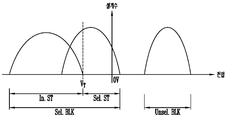
소거 동작은 소거전압을 점진적으로 높이면서 소거전압을 인가하는 동작과 소거 검증동작을 반복하는 ISPE(Incremental Step Pulse Erase) 방법으로 수행한다. 소거 동작이 시작되면, 선택된 메모리 블록(Sel. BLK)에 포함된 메모리 셀들을 소거하기 위하여 모든 비트라인들(BL)과 소오스라인들(SL)에 소거전압을 인가하고, 모든 드레인 셀렉트 라인들(도 3의 DSL1~DSL3) 및 소오스라인들(도 3의 SSL1~SSL3)에 턴온전압(예컨대, 15V의 전압)을 인가하고, 선택된 메모리 블록(Sel. BLK)의 워드라인들(WL1~WL32)에는 소거 허용 전압(예컨대, 0V의 전압)을 인가하고, 비선택된 메모리 블로들(Unsel. BLK)에는 소거 금지 전압(예컨대, 18V의 전압)을 인가한다. 제1 실시예에서는, 비트라인들(BL) 및 소오스라인들(SL)에 인가하는 소거전압과 동일한 전압을 소거 금지 전압으로 사용하는데, 예를 들면 소거전압 및 소거 금지 전압으로 18V의 전압을 사용할 수 있다.
The erase operation is performed by an incremental step pulse erase (ISPE) method in which the erase voltage is applied while the erase voltage is gradually increased and the erase verify operation is repeated. When the erase operation is started, an erase voltage is applied to all the bit lines BL and the source lines SL to erase the memory cells included in the selected memory block (Sel. BLK), all the drain select lines (For example, voltage of 15V) is applied to the source lines (DSL1 to DSL3 in Fig. 3) and the source lines (SSL1 to SSL3 in Fig. 3) and the word lines WL1 to WL32 of the selected memory block (For example, a voltage of 0V) is applied to the non-selected memory blobs (Unsel. BLK) and a erase prohibition voltage (e.g., a voltage of 18V) is applied to the non-selected memory blobs Unsel. In the first embodiment, a voltage equal to the erase voltage applied to the bit lines BL and the source lines SL is used as the erase prohibition voltage. For example, a voltage of 18V is used as the erase voltage and erase prohibition voltage .
다음의 '표3'을 참조하여 소거 동작을 구체적으로 설명하도록 한다. The erase operation will be described in detail with reference to Table 3 below.
'표3'을 참조하면, 소거 동작이 시작되면 모든 메모리 블록들(Sel. BLK 및 Unsel. BLK)에 연결된 비트라인들(BL) 및 소오스라인들(SL)에 소거전압(Verase)을 인가하고, 드레인 셀렉트 라인들(DSL)과 소오스 셀렉트 라인들(SSL)에는 드레인 턴온전압(Vdsl) 및 소오스 턴온전압(Vssl)을 인가한다. 선택된 메모리 블록(Sel. BLK)에 연결된 모든 워드라인들(WL1 내지 WL32)에는 소거 허용전압을 인가하고, 선택된 메모리 블록(Sel. BLK)을 제외한 나머지 비선택된 메모리 블록들(Unsel. BLK)에는 비선택된 셀 스트링들(Unsel. ST)만 포함되어 있으므로, 비선택된 셀 스트링들(Unsel. ST)에 연결된 모든 워드라인들(WL1 내지 WL32)에는 소거 금지전압(Vwl)을 인가한다. 예를 들면, 소거전압(Verase)은 18V, 드레인 및 소오스 턴온전압들(Vdsl 및 Vssl)은 15V, 소거 허용전압은 0V, 소거 금지전압(Vwl)은 소거전압(Verase)과 동일한 전압으로 설정하거나 드레인 및 소오스 턴온전압들(Vdsl 및 Vssl)보다 낮고 0V보다 높은 전압으로 설정할 수 있다. 소거전압(Verase)과 드레인 및 소오스 턴온전압들(Vdsl 및 Vssl)은 반도체 장치에 따라 변경될 수 있으나, 소거 금지전압(Vwl)을 드레인 및 소오스 턴온전압들(Vdsl 및 Vssl)보다 낮고 0V보다 높은 전압으로 설정할 경우, 소거 금지전압(Vwl)은 약 13.5V의 전압으로 설정할 수 있다. 비트라인들(BL)과 소오스라인들(SL)에 소거전압(Verase)을 인가하기 위해서는, 소거전압(Verase)을 갖는 제1 및 제2 전압(도 4 참조)을 비트라인들(BL) 및 소오스라인들(SL)에 인가한다. Referring to Table 3, when the erase operation is started, an erase voltage Verase is applied to the bit lines BL and the source lines SL connected to all the memory blocks (Sel. BLK and Unsel. BLK) The drain turn-on voltage Vdsl and the source turn-on voltage Vssl are applied to the drain select lines DSL and the source select lines SSL. The erase enable voltage is applied to all the word lines WL1 to WL32 connected to the selected memory block Sel.BLK and the non-selected memory blocks Unsel.BLK except for the selected memory block Sel.BLK, The erase prohibition voltage Vwl is applied to all the word lines WL1 to WL32 connected to the unselected cell strings Unsel. ST since only the selected cell strings Unsel. For example, the erase voltage Verase is set to 18V, the drain and source turn-on voltages Vdsl and Vssl are set to 15V, the erase permitting voltage is set to 0V, the erase prohibition voltage Vwl is set to the same voltage as the erase voltage Verase Drain and source turn-on voltages Vdsl and Vssl and higher than 0V. The erase voltage Verase and the drain and source turn-on voltages Vdsl and Vssl may vary depending on the semiconductor device, but the erase prohibition voltage Vwl may be lower than the drain and source turn-on voltages Vdsl and Vssl, When set to a voltage, the erase prohibition voltage Vwl can be set to a voltage of about 13.5V. In order to apply the erase voltage Verase to the bit lines BL and the source lines SL, first and second voltages (see FIG. 4) having an erase voltage Verase are applied to the bit lines BL and To the source lines SL.
소거 동작은 ISPE 방식으로 수행되므로, 비트라인들(BL) 및 소오스라인들(SL)을 통해 소거전압을 인가한 후에는 소거 검증동작을 수행한다. 소거 검증동작은 셀 스트링 단위로 수행하되, 비트라인(BL)에 공통으로 연결된 셀 스트링들 단위로 수행한다. 즉, 소거 검증동작은 도 3에서 상술한 셀 스트링 그룹(CSG) 단위로 수행한다. Since the erase operation is performed by the ISPE method, the erase verify operation is performed after the erase voltage is applied through the bit lines BL and the source lines SL. The erase verify operation is performed in units of cell strings, but in units of cell strings connected in common to the bit lines BL. That is, the erase verify operation is performed on the cell string group (CSG) basis described above with reference to FIG.
소거 검증동작이 패스된 셀 스트링들은 소거 억제 셀 스트링들(In. ST; Inhibit String)이 되고, 소거 억제 셀 스트링들(In. ST)에 연결된 비트라인들(BL)과 소오스라인들(SL)은 각각 소거 억제 비트라인들(In. BL) 및 소거 억제 소오스라인들(In. SL)로 정의된다. 소거 검증동작이 패스되지 않은 셀 스트링들(ST)은 선택된 셀 스트링들(Sel. ST)로 정의되며, 선택된 셀 스트링들(Sel. ST)에 연결된 비트라인들(BL) 및 소오스라인들(SL)은 각각 선택 비트라인들(Sel. BL) 및 선택 소오스 들(Sel. SL)로 정의된다. 도 6을 참조하면, 선택된 메모리 블록들(Sel. BLK)에 포함된 메모리 셀들은 소거 동작이 이루어지므로 문턱전압이 낮아진다. 메모리 셀들의 문턱전압이 소거 목표전압(VT)까지 낮아지면 해당 메모리 셀은 소거가 완료된다. 다만, 셀 스트링에는 다수의 메모리 셀들이 포함되어 있으므로, 셀 스트링에 포함된 모든 메모리 셀들의 문턱전압이 소거 목표전압(VT)까지 낮아져야만 해당 셀 스트링의 소거 검증동작이 패스되어 소거 억제 셀 스트링(In. ST)이 될 수 있다. 선택된 메모리 블록들(Sel. BLK)의 소거 동작이 수행되는 동안, 비선택된 메모리 블록들(Unsel. BLK)에 포함된 프로그램 메모리 셀들의 문턱전압은 그대로 유지된다. The cell strings passed through the erase verify operation become erase inhibition cell strings IN and the bit lines BL connected to the erase inhibition cell strings IN are connected to the source lines SL, Are defined as erase suppression bit lines IN. BL and erase suppression source lines IN SL, respectively. The cell strings ST that have not been subjected to the erase verify operation are defined by the selected cell strings Sel.ST and the bit lines BL connected to the selected cell strings Sel.ST and the source lines SL Are defined as select bit lines (Sel.LB) and select sources (Sel.SL), respectively. Referring to FIG. 6, the memory cells included in the selected memory blocks (Sel. BLK) are erased to lower the threshold voltage. When the threshold voltage of the memory cells is lowered to the erase target voltage (V T ), the erasing of the memory cell is completed. Since the cell string includes a plurality of memory cells, if the threshold voltage of all the memory cells included in the cell string is lowered to the erase target voltage V T , the erase verify operation of the corresponding cell string is passed, (In. ST). During the erase operation of the selected memory blocks (Sel.BLK), the threshold voltages of the program memory cells included in the unselected memory blocks (Unsel.BLK) are maintained.
소거 동작이 수행되는 동안, 선택 비트라인들(Sel. BL) 및 선택 소오스라인들(Sel. SL)에는 소거전압을 인가하여 선택된 셀 스트링들(Sel. ST)에 포함된 메모리 셀들을 소거하고, 소거 억제 비트라인들(In. BL) 및 소거 억제 소오스라인들(In. SL)에는 소거 억제 전압(Vinh)을 인가하여 소거 억제 셀 스트링들(In. ST)에 포함된 메모리 셀들의 문턱전압이 더 낮아지는 것을 억제한다. 이를 위해, 소거 억제 전압(Vinh)은 소거전압(Verase)보다 낮은 전압으로 설정하는데, 소거전압(Verase)의 1/2에 해당되는 전압으로 설정할 수 있다. 예를 들어, 소거전압(Verase)이 18V이면 소거 억제 전압(Vinh)은 9V로 설정될 수 있다. 이때, 선택된 메모리 블록(Sel. BLK)에 연결된 모든 워드라인들(WL1 내지 WL32)에는 소거 허용전압인 0V가 인가되므로, 소거 억제 셀 스트링들(In. ST)에서는 워드라인들(WL)과 채널 간의 전압 차이가 약 9V 발생할 수 있다. 9V의 전압 차이로는 소거 완료된 메모리 셀들의 문턱전압이 더 낮아지기 어려우므로 소거 완료된 메모리 셀들의 과도한 소거를 억제시킬 수 있다. During the erase operation, an erase voltage is applied to the selected bit lines (Sel.LB) and the selected source lines (Sel.SL) to erase the memory cells included in the selected cell strings (Sel.ST) The erase suppression voltage Vinh is applied to the erase suppression bit lines IN and BL and the threshold voltages of the memory cells included in the erase inhibition cell strings IN are Thereby suppressing further lowering. To this end, the erase suppression voltage Vinh is set to a voltage lower than the erase voltage Verase, but it can be set to a voltage corresponding to 1/2 of the erase voltage Verase. For example, when the erase voltage Verase is 18V, the erase suppression voltage Vinh can be set to 9V. At this time, since the erase allowable voltage of 0 V is applied to all the word lines WL1 to WL32 connected to the selected memory block (Sel. BLK), the word lines (WL) and the channel A voltage difference of about 9 V may occur between the two. The voltage difference of 9 V makes it difficult to lower the threshold voltage of the erased memory cells, thereby suppressing excessive erasure of the erased memory cells.
비선택된 메모리 블록들(Unsel. BLK)에 연결된 모든 워드라인들(WL1 내지 WL32)에는 소거 금지 전압(Vwl)이 인가되고 있으므로, 선택된 비트라인들(Sel. BL)에 소거전압(예컨대, 18V의 전압)이 인가되더라도 워드라인들(WL)과 채널 간의 전압차이가 많이 발생하지 않는다. 예를 들면, 소거 금지 전압(Vwl)이 소거전압(Verase)과 동일한 경우, 워드라인들(WL)과 채널 간의 전압 차이는 0V가 되므로 메모리 셀들은 소거되지 않는다. 또한, 소거 금지전압(Vwl)을 상술한 바와 같이 약 13.5V의 전압으로 설정할 경우, 워드라인들(WL)과 채널 간의 전압 차이는 4.5V가 되는데, 4.5V의 전압 차이로는 메모리 셀들이 소거되지 않는다. The erase prohibition voltage Vwl is applied to all the word lines WL1 to WL32 connected to the unselected memory blocks Unsel.BLK, The voltage difference between the word lines WL and the channel does not occur much. For example, when the erase prohibition voltage Vwl is equal to the erase voltage Verase, the voltage difference between the word lines WL and the channel becomes 0V, so that the memory cells are not erased. Also, when the erase prohibition voltage Vwl is set to a voltage of about 13.5 V as described above, the voltage difference between the word lines WL and the channel becomes 4.5 V. At a voltage difference of 4.5 V, It does not.
또한, 비선택된 메모리 블록들(Unsel. BLK)에 연결된 소거 억제 비트라인들(In. BL) 및 소거 억제 소오스라인들(In. SL)에는 소거 억제 전압(9V)이 인가되고 있으므로, 워드라인들(WL1 내지 WL32)에 소거전압(Verase)과 동일한 소거 금지 전압(Vwl)이 인가되더라도 워드라인들과 채널 간의 전압 차이가 약 9V가 발생하는데, 9V의 전압 차이로는 메모리 셀들이 소거되지 않으므로 비선택된 메모리 블록들(Unsel. BLK)에 포함된 메모리 셀들의 소거를 금지할 수 있다. 만약, 소거 금지전압(Vwl)을 13.5V로 설정하더라도 워드라인들과 채널 간의 전압 차이는 약 4.5V가 되므로 메모리 셀들의 소거를 금지할 수 있다. Since erase suppression voltage 9V is applied to erase suppression bit lines IN. BL connected to unselected memory blocks Unsel BLK and erase suppression source lines IN SL, Even if the erase prohibition voltage Vwl equal to the erase voltage Verase is applied to the word lines WL1 to WL32, a voltage difference of about 9 V occurs between the word lines and the channel. However, since the memory cells are not erased at a voltage difference of 9 V, The erase of the memory cells included in the selected memory blocks Unsel.BLK can be inhibited. Even if the erase prohibition voltage Vwl is set to 13.5 V, the voltage difference between the word lines and the channel becomes about 4.5 V, so that the erasing of the memory cells can be prohibited.
상술한 소거 동작을 반복하여 선택된 메모리 블록(Sel. BLK)에 포함된 모든 메모리 셀들이 소거 검증동작을 패스하면 소거 동작이 종료된다. When the above-described erase operation is repeated and all the memory cells included in the selected memory block Sel.BLK pass the erase verify operation, the erase operation is ended.
상술한 바와 같이, 소거 완료된 셀 스트링들의 과소거를 억제함으로써 소거 완료된 메모리 셀들의 문턱전압 분포 폭이 증가하는 것을 억제할 수 있고, 소거 대상이 아닌 비선택된 메모리 셀들의 소거전압에 의한 스트레스를 억제할 수 있다.
As described above, it is possible to suppress the threshold voltage distribution width of the erased memory cells from being increased by suppressing the over erasing of the erased cell strings, and to suppress the stress due to the erase voltage of the non-selected memory cells .
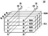
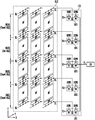
도 7은 본 발명의 제2 실시예에 따른 메모리 블록들의 구성을 설명하기 위한 도면이다. 7 is a view for explaining a configuration of memory blocks according to a second embodiment of the present invention.
도 7을 참조하면, 메모리 셀 어레이(110)는 다수의 메모리 블록들(BLK11~BLK44)을 포함한다. 제2 실시예에서는 메모리 블록들(BLK11~BLK44)이 복층으로 이루어지며, 서로 동일한 구성으로 이루어진다. 또한, 도 7에서는 설명의 편의를 위하여 종 방향으로 4개의 메모리 블록들이 배열되고, 수직방향으로 4개의 메모리 블록들이 배열된 구조를 도시하였으므로, 메모리 블록들의 개수는 반도체 장치에 따라 변경 가능하다. Referring to FIG. 7, the
메모리 블록들(BLK11~BLK44) 중, 수직 방향으로 적층된 메모리 블록들은 서로 워드라인들(WL)을 공유하지만, 종 방향으로 배열된 메모리 블록들에는 서로 다른 워드라인들(WL)이 연결된다. 예를 들면, 수직 방향으로 배열된 'BLK11~BLK41' 메모리 블록들은 동일한 워드라인들(WL)을 공유하지만, 종 방향으로 배열된 'BLK11~BLK14' 메모리 블록들에는 서로 다른 워드라인들(WL)이 연결된다. 따라서, 수직 방향으로 배열된 메모리 셀들에는 공통으로 연결된 워드라인들을 통하여 동일한 전압을 동시에 인가할 수 있으며, 종 방향으로 배열된 메모리 블록들의 워드라인들에는 서로 다른 전압을 동시에 인가할 수 있다. 또한, 종 방향으로 배열된 메모리 블록들은 비트라인들(BL)과 소오스라인들(SL)을 서로 공유한다. 수직 방향으로 배열된 비트라인들(BL) 및 소오스라인들(SL)은 선택 스위치부(150)에 공통으로 연결되며, 종 방향으로 배열된 비트라인들 또는 소오스라인들(SL)은 서로 다른 선택 스위치부(150)에 연결된다. 각각의 선택 스위치부(150)에는 페이지 버퍼(PB)가 각각 연결된다.
Among the memory blocks BLK11 to BLK44, the memory blocks stacked in the vertical direction share word lines WL, but different word lines WL are connected to the memory blocks arranged in the longitudinal direction. For example, 'BLK11 to BLK41' memory blocks arranged in the vertical direction share the same word lines (WL), but different word lines (WL) are arranged in the longitudinally arranged 'BLK11 to BLK14'Lt; / RTI > Therefore, the memory cells arranged in the vertical direction can simultaneously apply the same voltage through the commonly connected word lines, and simultaneously apply different voltages to the word lines of the vertically arranged memory blocks. Further, the memory blocks arranged in the longitudinal direction share the bit lines BL and the source lines SL with each other. The bit lines BL and the source lines SL arranged in the vertical direction are commonly connected to the
도 8은 도 7에 도시된 메모리 블록들을 구체적으로 설명하고, 제2 실시예에 따른 프로그램, 독출 및 소거 동작을 설명하기 위한 도면이다. 8 is a diagram for describing the memory blocks shown in FIG. 7 in detail and explaining the program, read and erase operations according to the second embodiment.
도 8을 참조하여, 수직 방향으로 적층된 메모리 블록들(BLK11, BLK21, BLK31, BLK41)을 예를 들어 설명하도록 한다. Referring to FIG. 8, the memory blocks BLK11, BLK21, BLK31, and BLK41 stacked in the vertical direction will be described as an example.
설명의 편의상 'BLK11'을 제1 메모리 블록이라 하고, 'BLK21'을 제2 메모리 블록이라 하고, 'BLK31'을 제3 메모리 블록(BLK113)이라 하고, 'BLK41'을 제4 메모리 블록이라 한다. 제1 내지 제4 메모리 블록들(BLK11 내지 BLK41)에 각각 연결된 소오스 셀렉트 라인(SSL), 워드라인(WL) 및 드레인 셀렉트 라인(DSL)은 서로 인접한 메모리 블록들이 서로 공유하는 소오스라인(SL) 또는 비트라인(BL)을 기준으로 서로 대칭이 되도록 배열된다. 각각의 메모리 블록들의 구체적인 구성을 설명하면 다음과 같다. For convenience of explanation, 'BLK11' is referred to as a first memory block, 'BLK21' is referred to as a second memory block, 'BLK31' is referred to as a third memory block BLK113, and 'BLK41' is referred to as a fourth memory block. The source select line SSL, the word line WL and the drain select line DSL connected to the first to fourth memory blocks BLK11 to BLK41 are connected to the source line SL or the drain line SL, Are arranged to be symmetrical with respect to the bit line BL. A specific configuration of each memory block will be described below.
제1 메모리 블록(BLK11)의 하부에는 소오스라인들(SL)이 배열되고, 소오스라인들(SL)의 상부에 소오스 셀렉트 트랜지스터들(SST)이 배열된다. 소오스 셀렉트 트랜지스터들(SST)의 상부에는 메모리 셀들(MC)이 배열되고, 메모리 셀들(MC)의 상부에 드레인 셀렉트 트랜지스터들(DST)이 배열된다. 드레인 셀렉트 트랜지스터들DST)의 상부에는 비트라인들(BL)이 배열된다. 즉, 제1 메모리 블록(BLK11)에서는 하부에서 상부로 소오스라인들(SL), 소오스 셀렉트 라인들(SSL), 워드라인들(WL), 드레인 셀렉트 라인들(DSL) 및 비트라인들(BL)이 순차적으로 배열된다. The source lines SL are arranged below the first memory block BLK11 and the source select transistors SST are arranged above the source lines SL. Memory cells MC are arranged above the source select transistors SST and drain select transistors DST are arranged above the memory cells MC. The bit lines BL are arranged above the drain select transistors DST. That is, in the first memory block BLK11, the source lines SL, the source select lines SSL, the word lines WL, the drain select lines DSL, and the bit lines BL, Are sequentially arranged.
제2 메모리 블록(BLK21)은 제1 메모리 블록(BLK11)의 상부에 적층되는데, 제1 메모리 블록(BLK11)의 비트라인들(BL)을 공유한다. 따라서, 제2 메모리 블록(BLK21)에서는 비트라인들(BL)이 하단에 배열되고, 비트라인들(BL)의 상부에 드레인 셀렉트 라인들(DSL), 워드라인들(WL), 소오스 셀렉트 라인들(SSL) 및 소오스라인들(SL)이 순차적으로 배열된다. The second memory block BLK21 is stacked on the first memory block BLK11 and shares the bit lines BL of the first memory block BLK11. Accordingly, in the second memory block BLK21, the bit lines BL are arranged at the lower stage and the drain select lines DSL, word lines WL, source select lines (SSL) and source lines SL are sequentially arranged.
제3 메모리 블록(BLK31)은 제2 메모리 블록(BLK21)의 상부에 적층되는데, 제2 메모리 블록(BLK21)의 소오스라인들(SL)을 공유한다. 따라서, 제3 메모리 블록(BLK31)에서는 소오스라인들(SL)이 하단에 배열되고, 소오스라인들(SL)의 상부에 소오스 셀렉트 라인들(SSL), 워드라인들(WL), 드레인 셀렉트 라인들(DSL) 및 비트라인들(BL)이 순차적으로 배열된다. The third memory block BLK31 is stacked on the second memory block BLK21 and shares the source lines SL of the second memory block BLK21. Therefore, in the third memory block BLK31, the source lines SL are arranged at the lower stage, and the source select lines SSL, the word lines WL, the drain select lines SL, (DSL) and bit lines (BL) are sequentially arranged.
제4 메모리 블록(BLK41)은 제3 메모리 블록(BLK31)의 상부에 적층되는데, 제3 메모리 블록(BLK31)의 비트라인들(BL)을 공유한다. 따라서, 제4 메모리 블록(BLK41)에서는 비트라인들(BL)이 하단에 배열되고, 비트라인들(BL)의 상부에 드레인 셀렉트 라인들(DSL), 워드라인들(WL), 소오스 셀렉트 라인들(SSL) 및 소오스라인들(SL)이 순차적으로 배열된다. The fourth memory block BLK41 is stacked on the third memory block BLK31 and shares the bit lines BL of the third memory block BLK31. Accordingly, in the fourth memory block BLK41, the bit lines BL are arranged at the lower stage and the drain select lines DSL, word lines WL, source select lines (SSL) and source lines SL are sequentially arranged.
또한, 제1 내지 제4 메모리 블록들(BLk11 내지 BLK41)에 포함된 메모리 셀들(MC)도 제1 그룹 및 제2 그룹으로 구분되며, 서로 인접한 메모리 블록들의 제1 및 제2 그룹도 서로 대칭으로 배열된다. 예를 들면, 제1 메모리 블록(BLK11)에서 제1 그룹이 하부에 배열되고 제2 그룹이 상부에 배열되면, 제2 메모리 블록(BLK21)에서는 하부에 제2 그룹이 배열되고 상부에 제1 그룹이 배열된다. The memory cells MC included in the first to fourth memory blocks BLk11 to BLK41 are also divided into a first group and a second group and the first and second groups of memory blocks adjacent to each other are also symmetrical . For example, in the first memory block BLK11, the first group is arranged at the lower part and the second group is arranged at the upper part. In the second memory block BLK21, the second group is arranged at the lower part, .
선택 스위치부(150)는 제1 내지 제 5 선택회로들(BS1 내지 BS5)을 포함한다. 제1 내지 제5 선택회로들(BS1 내지 BS5)은 서로 동일하게 구성되는데, 제1 내지 제5 전압들(V1 내지 V5)을 각각 공급받고, 공통으로 연결된 페이지 라인(PL)을 통하여 페이지 버퍼(PB)에 연결된다. The
제1 선택회로(BS1)는 제1 전압(V1) 또는 페이지 버퍼(PB)로부터 전달된 전압을 제1 메모리 블록(BLK11)의 소오스라인(SL)에 선택적으로 전달하도록 구성된다.구체적으로, 제1 선택회로(BS1)는 제1 전압(V1)이 인가되는 단자와 페이지 라인(PL) 사이에서 서로 직렬로 연결된 제1 및 제2 스위치들(81 및 82)을 포함한다. 제1 스위치(81)는 제1 소오스라인 선택신호(SSW1)에 응답하여 동작하는 NMOS 트랜지스터로 구현될 수 있고, 제2 스위치(82)는 제2 소오스라인 선택신호(SSW2)에 응답하여 동작하는 NMOS 트랜지스터로 구현될 수 있다. 제1 메모리 블록(BLK11)의 소오스라인(SL)은 제1 및 제2 스위치들(81 및 82) 사이에 연결된다. The first selection circuit BS1 is configured to selectively transmit the voltage supplied from the first voltage V1 or the page buffer PB to the source line SL of the first memory block BLK11. 1 selection circuit BS1 includes first and
제2 선택회로(BS2)는 제2 전압(V2) 또는 페이지 버퍼(PB)로부터 전달된 전압을 제1 및 제2 메모리 블록들(BLK11 및 BLK21)이 공유하는 비트라인(BL)에 선택적으로 전달하도록 구성된다. 구체적으로, 제2 선택회로(BS2)는 제2 전압(V2)이 인가되는 단자와 페이지 라인(PL) 사이에서 서로 직렬로 연결된 제3 및 제4 스위치들(83 및 84)을 포함한다. 제3 스위치(83)는 제1 비트라인 선택신호(BSW1)에 응답하여 동작하는 NMOS 트랜지스터로 구현될 수 있고, 제4 스위치(84)는 제2 비트라인 선택신호(BSW2)에 응답하여 동작하는 NMOS 트랜지스터로 구현될 수 있다. 제1 및 제2 메모리 블록들(BLK11 및 BLK21)이 공유하는 비트라인(BL)은 제3 및 제4 스위치들(83 및 84) 사이에 연결된다. The second selection circuit BS2 selectively transfers the voltage delivered from the second voltage V2 or the page buffer PB to the bit line BL shared by the first and second memory blocks BLK11 and BLK21 . Specifically, the second selection circuit BS2 includes third and
제3 선택회로(BS3)는 제3 전압(V3) 또는 페이지 버퍼(PB)로부터 전달된 전압을 제2 및 제3 메모리 블록들(BLK21 및 BLK31)이 공유하는 소오스라인(SL)에 선택적으로 전달하도록 구성된다. 구체적으로, 제3 선택회로(BS3)는 제3 전압(V3)이 인가되는 단자와 페이지 라인(PL) 사이에서 서로 직렬로 연결된 제5 및 제6 스위치들(85 및 86)을 포함한다. 제5 스위치(85)는 제3 소오스라인 선택신호(SSW3)에 응답하여 동작하는 NMOS 트랜지스터로 구현될 수 있고, 제6 스위치(86)는 제4 소오스라인 선택신호(SSW2)에 응답하여 동작하는 NMOS 트랜지스터로 구현될 수 있다. 제2 및 제3 메모리 블록들(BLK21 및 BLK31)이 공유하는 소오스라인(SL)은 제5 및 제6 스위치들(85 및 86) 사이에 연결된다. The third selection circuit BS3 selectively transmits the voltage from the third voltage V3 or the page buffer PB to the source line SL shared by the second and third memory blocks BLK21 and BLK31 . Specifically, the third selection circuit BS3 includes fifth and
제4 선택회로(BS4)는 제4 전압(V4) 또는 페이지 버퍼(PB)로부터 전달된 전압을 제3 및 제4 메모리 블록들(BLK31 및 BLK41)이 공유하는 비트라인(BL)에 선택적으로 전달하도록 구성된다. 구체적으로, 제4 선택회로(BS4)는 제4 전압(V4)이 인가되는 단자와 페이지 라인(PL) 사이에서 서로 직렬로 연결된 제7 및 제8 스위치들(87 및 88)을 포함한다. 제7 스위치(87)는 제3 비트라인 선택신호(BSW3)에 응답하여 동작하는 NMOS 트랜지스터로 구현될 수 있고, 제8 스위치(88)는 제4 비트라인 선택신호(BSW4)에 응답하여 동작하는 NMOS 트랜지스터로 구현될 수 있다. 제3 및 제4 메모리 블록들(BLK31 및 BLK41)이 공유하는 비트라인(BL)은 제7 및 제8 스위치들(87 및 88) 사이에 연결된다. The fourth selection circuit BS4 selectively transfers the voltage supplied from the fourth voltage V4 or the page buffer PB to the bit line BL shared by the third and fourth memory blocks BLK31 and BLK41 . Specifically, the fourth selection circuit BS4 includes seventh and
제5 선택회로(BS5)는 제5 전압(V5) 또는 페이지 버퍼(PB)로부터 전달된 전압을 제4 메모리 블록(BLK41)에 연결된 소오스라인(SL)에 선택적으로 전달하도록 구성된다. 구체적으로, 제5 선택회로(BS5)는 제5 전압(V5)이 인가되는 단자와 페이지 라인(PL) 사이에서 서로 직렬로 연결된 제9 및 제10 스위치들(89 및 90)을 포함한다. 제9 스위치(89)는 제5 소오스라인 선택신호(SSW5)에 응답하여 동작하는 NMOS 트랜지스터로 구현될 수 있고, 제10 스위치(90)는 제6 소오스라인 선택신호(SSW4)에 응답하여 동작하는 NMOS 트랜지스터로 구현될 수 있다. 제4 메모리 블록(BLK41)에 연결된 소오스라인(SL)은 제9 및 제10 스위치들(89 및 90) 사이에 연결된다.
The fifth selection circuit BS5 is configured to selectively transmit the voltage delivered from the fifth voltage V5 or the page buffer PB to the source line SL connected to the fourth memory block BLK41. Specifically, the fifth selection circuit BS5 includes ninth and
다음의 표4'를 참조하여 선택된 메모리 블록(Sel. BLK)의 프로그램 동작을 설명하도록 한다. The program operation of the selected memory block (Sel. BLK) will be described with reference to Table 4 '.
BLK41
(Unsel. BLK)
BLK41
(Unsel BLK)
(제1그룹)WL
(First group)
VpassVpgm /
Vpass
VpassVpgm /
Vpass
VpassVpgm /
Vpass
(제2그룹)WL
(Second group)
VpassVpgm /
Vpass
VpassVpgm /
Vpass
VpassVpgm /
Vpass
BLK31BLK31
((
SelSel
. .
BLKBLK
))
(제2그룹)WL
(Second group)
VpassVpgm /
Vpass
VpassVpgm /
Vpass
VpassVpgm /
Vpass
(제1그룹)WL
(First group)
VpassVpgm /
Vpass
VpassVpgm /
Vpass
VpassVpgm /
Vpass
BLK21
(Unsel. BLK)
BLK21
(Unsel BLK)
(제1그룹)WL
(First group)
VpassVpgm /
Vpass
VpassVpgm /
Vpass
VpassVpgm /
Vpass
(제2그룹)WL
(Second group)
VpassVpgm /
Vpass
VpassVpgm /
Vpass
VpassVpgm /
Vpass
BLK11
(Unsel. BLK)
BLK11
(Unsel BLK)
(제2그룹)WL
(Second group)
VpassVpgm /
Vpass
VpassVpgm /
Vpass
VpassVpgm /
Vpass
(제1그룹)WL
(First group)
VpassVpgm /
Vpass
VpassVpgm /
Vpass
VpassVpgm /
Vpass
'표4'를 참조하면, 선택된 메모리 블록(Sel. BLK)의 프로그램 동작은 '표1'에서 상술한 바와 같이 메모리 셀들을 제1 및 제2 그룹으로 구분하여 실시한다. 예를 들면, 제1 그룹의 메모리 셀들은 소오스 셀렉트 라인(SSL)에 인접한 메모리 셀부터 중앙방향의 메모리 셀 순서로 프로그램 동작을 실시한다. 따라서, 제1 그룹의 메모리 셀들을 프로그램하는 동안, 제1 그룹의 메모리 셀들에 연결된 워드라인들(WL)에는 프로그램 전압(Vpgm) 또는 패스전압(Vpass)이 인가되고, 제2 그룹의 메모리 셀들에 연결된 워드라인들(WL)에는 패스전압(Vapss)이 인가된다. 제2 그룹의 메모리 셀들을 프로그램하는 동안, 제2 그룹의 메모리 셀들에 연결된 워드라인들(WL)에는 프로그램 전압(Vpgm) 또는 패스전압(Vpass)이 인가되고, 제1 그룹의 메모리 셀들에 연결된 워드라인들(WL)에는 패스전압(Vpass)이 인가된다. Referring to Table 4, the program operation of the selected memory block (Sel. BLK) is performed by dividing the memory cells into the first and second groups as described in Table 1. For example, the first group of memory cells performs a program operation in the order from the memory cell adjacent to the source select line (SSL) to the memory cell in the center direction. Thus, during programming of the first group of memory cells, the program voltage Vpgm or the pass voltage Vpass is applied to the word lines WL connected to the first group of memory cells, A pass voltage Vapss is applied to the connected word lines WL. During programming of the second group of memory cells, the program voltage Vpgm or the pass voltage Vpass is applied to the word lines WL connected to the memory cells of the second group, A pass voltage Vpass is applied to the lines WL.
특히, 제1 내지 제4 메모리 블록들(BLK11 내지 BLK41)은 워드라인들을 공유하기 때문에, 선택된 메모리 블록(Sel. BLK)의 선택된 워드라인에 프로그램 전압(Vpgm)을 인가하면 비선택된 메모리 블록의 해당 워드라인에도 프로그램 전압(Vpgm)이 인가된다. 따라서, 비선택된 메모리 블록들(Unsel. BLK)에 포함된 메모리 셀들이 프로그램되지 않도록 비트라인들(BL), 소오스라인들(SL), 드레인 셀렉트 라인들(DSL) 및 소오스 셀렉트 라인들(SSL)에 인가하는 전압을 조절한다.
In particular, since the first to fourth memory blocks BLK11 to BLK41 share the word lines, if the program voltage Vpgm is applied to the selected word line of the selected memory block Sel.BLK, The program voltage Vpgm is also applied to the word line. Therefore, the bit lines BL, the source lines SL, the drain select lines DSL and the source select lines SSL are set such that the memory cells included in the unselected memory blocks Unsel.BLK are not programmed. The voltage to be applied to the capacitor is adjusted.
제1 그룹 및 제2 그룹의 프로그램 동작을 구체적으로 설명하면 다음과 같다. The program operation of the first group and the second group will be described in detail as follows.
제1 그룹의 프로그램 동작Program operation of the first group
선택된 메모리 블록(Sel. BLK)인 제3 메모리 블록(BLK31)에서 제1 그룹의 프로그램 동작을 수행하는 동안, 제3 메모리 블록(BLK31)에 연결된 소오스라인들(SL)에는 전원전압(VCC)을, 소오스 셀렉트 라인들(SSL)에는 턴오프전압(예컨대, 0V)을, 워드라인들(WL)에는 프로그램 전압(Vpgm) 또는 패스전압(Vpass)을, 드레인 셀렉트 라인들(DSL)에는 드레인 턴온전압(Vdsl; 예컨대, 4V)을, 비트라인들(BL)에는 프로그램 허용전압(예컨대, 0V) 또는 프로그램 금지전압(예컨대, VCC)을 인가한다. The power supply voltage VCC is applied to the source lines SL connected to the third memory block BLK31 while the program operation of the first group is performed in the third memory block BLK31 which is the selected memory block Sel. A program voltage Vpgm or a pass voltage Vpass is applied to the word lines WL and a drain turn-on voltage Vcc is applied to the drain select lines DSL, (E.g., 4 V) to the bit lines BL and a program allowable voltage (e.g., 0 V) or the program inhibit voltage (e.g., VCC) to the bit lines BL.
비선택된 메모리 블록(Unsel. BLK)인 제4 메모리 블록(BLK41)에서는 비트라인들(BL)에 인가되는 전압들 중에서 프로그램 허용전압(예컨대, 0V)에 의해 제4 메모리 블록(BLK41)의 채널 전압이 낮아지는 것을 방지하기 위하여, 드레인 셀렉트 라인들(DSL)에 턴오프전압을 인가한다. 턴오프전압은 프로그램 허용전압과 같거나 낮은 전압 또는 음의 전압이 될 수 있다. 예를 들면, 턴오프전압은 0V 또는 -2V의 전압이 될 수 있으며, 반도체 장치에 따라 전압 레벨은 변경될 수도 있다. 제4 메모리 블록(BLK41)에 연결된 소오스라인들(SL)에는 프로그램 금지전압(예컨대, VCC)을 인가하고, 소오스 셀렉트 라인들(SSL)에는 소오스 턴온전압(Vssl)을 인가한다. 소오스 턴온전압(Vssl)은 처음에는 소오스라인들(SL)을 통하여 프로그램 금지전압을 채널에 충분히 전달하기 위하여 높은 레벨을 유지한 후, 0V보다 높되 처음의 높은 레벨보다는 낮아지도록 한다. 소오스 턴온전압(Vssl)이 낮아지면 소오스 셀렉트 트랜지스터들(SST)이 턴오프되면서 채널 부스팅이 발생한다. 이로써, 비선택된 제4 메모리 블록(BLK41)에 포함된 제1 그룹의 메모리 셀들은 프로그램되지 않는다. In the fourth memory block BLK41 which is a non-selected memory block (Unsel.BLK), the channel voltage of the fourth memory block BLK41 (for example, 0V) Off voltage is applied to the drain select lines DSL in order to prevent the drain select lines DSL from lowering. The turn-off voltage may be a voltage equal to or less than the program allowable voltage or a negative voltage. For example, the turn-off voltage may be a voltage of 0V or -2V, and the voltage level may be changed depending on the semiconductor device. A program inhibit voltage (for example, VCC) is applied to the source lines SL connected to the fourth memory block BLK41 and a source turn-on voltage Vssl is applied to the source select lines SSL. The source turn-on voltage Vssl is initially maintained at a high level to sufficiently transmit the program inhibit voltage to the channel through the source lines SL, and then becomes higher than 0V but lower than the first high level. When the source turn-on voltage Vssl is lowered, the source select transistors SST are turned off and channel boosting occurs. As a result, the first group of memory cells included in the non-selected fourth memory block BLK41 are not programmed.
비선택된 메모리 블록(Unsel. BLK)인 제2 메모리 블록(BLK21)에서는 소오스 셀렉트 라인들(SSL)에 턴오프전압을 인가하여 소오스 셀렉트 트랜지스터들(SST)을 턴오프시킨다. 예를 들면, 턴오프전압은 0V이 전압이 될 수 있다. 제2 메모리 블록(BLK21)에 연결된 비트라인들(BL)에는 프로그램 금지전압(예컨대, VCC)을 인가하고, 드레인 셀렉트 라인들(DSL)에는 드레인 턴온전압(Vdsl)을 인가하여 제2 메모리 블록(BLK21)의 채널 전압을 상승시킨다. 드레인 턴온전압(Vdsl)은 처음에는 비트라인들(BL)을 통하여 프로그램 금지전압을 채널에 충분히 전달하기 위하여 높은 레벨을 유지한 후, 0V보다 높되 처음의 높은 레벨보다는 낮아지도록 한다. 드레인 턴온전압(Vdsl)이 낮아지면 드레인 셀렉트 트랜지스터들(DST)이 턴오프되면서 채널 부스팅이 발생한다. 이로써, 비선택된 제2 메모리 블록(BLK21)에 포함된 제1 그룹의 메모리 셀들은 프로그램되지 않는다. In the second memory block BLK21, which is a non-selected memory block (Unsel.BLK), a turn-off voltage is applied to the source select lines (SSL) to turn off the source select transistors (SST). For example, the turn-off voltage may be 0V. A program inhibition voltage (for example, VCC) is applied to the bit lines BL connected to the second memory block BLK21 and a drain turn-on voltage Vdsl is applied to the drain select lines DSL, BLK21). The drain turn-on voltage Vdsl is initially maintained at a high level to sufficiently transfer the program inhibit voltage through the bit lines BL to the channel, and then becomes higher than 0V but lower than the first high level. When the drain turn-on voltage Vdsl is lowered, the drain select transistors DST are turned off and channel boosting occurs. As a result, the first group of memory cells included in the non-selected second memory block BLK21 are not programmed.
비선택된 메모리 블록(Unsel. BLK)인 제1 메모리 블록(BLK11)에서는 채널 전압이 낮아지는 것을 방지하기 위하여, 소오스라인들(SL)에 전원전압(VCC)을 인가하고, 소오스 셀렉트 라인들(SSL)에는 턴오프전압(예컨대, 0V)을 인가하여 소오스 셀렉트 트랜지스터들(SST)을 턴오프시킨다. 비트라인들(BL)에 프로그램 금지전압(예컨대, VCC)이 인가되므로, 드레인 셀렉트 라인들(DSL)에는 드레인 턴온전압(Vdsl)을 인가하여 드레인 셀렉트 트랜지스터들(DST)을 턴온시킨다. 드레인 턴온전압(Vdsl)은 처음에는 비트라인들(BL)을 통하여 프로그램 금지전압을 채널에 충분히 전달하기 위하여 높은 레벨을 유지한 후, 0V보다 높되 처음의 높은 레벨보다는 낮아지도록 한다. 드레인 턴온전압(Vdsl)이 낮아지면 드레인 셀렉트 트랜지스터들(DST)이 턴오프되면서 채널 부스팅이 발생한다. 이로써, 비선택된 제1 메모리 블록(BLK11)에 포함된 제1 그룹의 메모리 셀들은 프로그램되지 않는다. In order to prevent the channel voltage from being lowered in the first memory block BLK11 which is a non-selected memory block Unsel.BLK, the power source voltage VCC is applied to the source lines SL, and the source select lines SSL (For example, 0V) to turn off the source select transistors SST. The drain turn-on voltage Vdsl is applied to the drain select lines DSL to turn on the drain select transistors DST since the program inhibit voltage (e.g., VCC) is applied to the bit lines BL. The drain turn-on voltage Vdsl is initially maintained at a high level to sufficiently transfer the program inhibit voltage through the bit lines BL to the channel, and then becomes higher than 0V but lower than the first high level. When the drain turn-on voltage Vdsl is lowered, the drain select transistors DST are turned off and channel boosting occurs. As a result, the first group of memory cells included in the non-selected first memory block BLK11 are not programmed.
제2 그룹의 프로그램 동작The program operation of the second group
선택된 메모리 블록(Sel. BLK)인 제3 메모리 블록(BLK31)에서 제1 그룹의 프로그램 동작이 완료되면, 제2 그룹의 프로그램 동작을 수행한다. When the program operation of the first group is completed in the third memory block BLK31 which is the selected memory block (Sel. BLK), the program operation of the second group is performed.
제2 그룹의 프로그램동작을 수행하는 동안, 제3 메모리 블록(BLK31)에 연결된 비트라인들(BL)에는 전원전압(VCC)을, 드레인 셀렉트 라인들(DSL)에는 턴오프전압(예컨대, 0V)을, 워드라인들(WL)에는 프로그램 전압(Vpgm) 또는 패스전압(Vpass)을, 소오스 셀렉트 라인들(SSL)에는 소오스 턴온전압(Vssl; 예컨대, 4V)을, 소오스라인들(SL)에는 프로그램 허용전압(예컨대, 0V) 또는 프로그램 금지전압(예컨대, VCC)을 인가한다. The power supply voltage VCC is applied to the bit lines BL connected to the third memory block BLK31 and the turn-off voltage (for example, 0V) is applied to the drain select lines DSL while the program operation of the second group is performed. A source turn-on voltage Vssl (for example, 4 V) is applied to the source select lines SSL, a program voltage Vpgm or a pass voltage Vpass is applied to the word lines WL, (E.g., 0 V) or a program inhibit voltage (e.g., VCC).
비선택된 메모리 블록(Unsel. BLK)인 제4 메모리 블록(BLK41)에서는 소오스라인들(SL)에 프로그램 금지전압(예컨대, VCC)을 인가하고, 소오스 셀렉트 라인들(SSL)에는 소오스 턴온전압(Vssl)을 인가한다. 비트라인들(BL)에는 전원전압(VCC)이 인가되고 있으므로, 드레인 셀렉트 라인들(DSL)에는 턴오프전압(예컨대, 0V)을 인가한다. 드레인 턴온전압(Vdsl)은 처음에는 비트라인들(BL)을 통하여 프로그램 금지전압을 채널에 충분히 전달하기 위하여 높은 레벨을 유지한 후, 0V보다 높되 처음의 높은 레벨보다는 낮아지도록 한다. 드레인 턴온전압(Vdsl)이 낮아지면 드레인 셀렉트 트랜지스터들(DST)이 턴오프되면서 채널 부스팅이 발생한다. 이로써, 비선택된 제4 메모리 블록(BLK41)에 포함된 제2 그룹의 메모리 셀들은 프로그램되지 않는다. In the fourth memory block BLK41 which is a non-selected memory block (Unsel.BLK), a program inhibition voltage (for example, VCC) is applied to the source lines SL and a source turn-on voltage Vssl ). Since the power supply voltage VCC is applied to the bit lines BL, a turn-off voltage (for example, 0 V) is applied to the drain select lines DSL. The drain turn-on voltage Vdsl is initially maintained at a high level to sufficiently transfer the program inhibit voltage through the bit lines BL to the channel, and then becomes higher than 0V but lower than the first high level. When the drain turn-on voltage Vdsl is lowered, the drain select transistors DST are turned off and channel boosting occurs. As a result, the memory cells of the second group included in the non-selected fourth memory block BLK41 are not programmed.
비선택된 메모리 블록(Unsel. BLK)인 제2 메모리 블록(BLK21)에서는 소오스라인들(SL)에 프로그램 금지전압(예컨대, VCC) 또는 프로그램 허용전압(예컨대, 0V)이 인가되므로, 소오스 셀렉트 라인들(SSL)에는 턴오프전압(예컨대, 0V)을 인가한다. 턴오프전압은 프로그램 허용전압과 같거나 낮은 전압 또는 음의 전압이 될 수 있다. 예를 들면, 턴오프전압은 0V 또는 -2V의 전압이 될 수 있으며, 반도체 장치에 따라 전압 레벨은 다양하게 변경될 수 있다. 제2 메모리 블록(BLK21)에 연결된 비트인들(BL)에는 프로그램 금지전압(예컨대, VCC)을 인가하고, 드레인 셀렉트 라인들(DSL)에는 드레인 턴온전압(Vdsl)을 인가한다. 드레인 턴온전압(Vdsl)은 처음에는 비트라인들(BL)을 통하여 프로그램 금지전압을 채널에 충분히 전달하기 위하여 높은 레벨로 유지한 후, 0V보다 높되 처음의 높은 레벨보다는 낮아지도록 한다. 드레인 턴온전압(Vdsl)이 낮아지면 드레인 셀렉트 트랜지스터들(DST)이 턴오프되면서 채널 부스팅이 발생한다. 이로써, 비선택된 제2 메모리 블록(BLK21)에 포함된 제2 그룹의 메모리 셀들은 프로그램되지 않는다. Since the program inhibit voltage (for example, VCC) or the program allowable voltage (for example, 0 V) is applied to the source lines SL in the second memory block BLK21 which is a non-selected memory block Unsel.BLK, (For example, 0 V) is applied to the data line SSL. The turn-off voltage may be a voltage equal to or less than the program allowable voltage or a negative voltage. For example, the turn-off voltage may be a voltage of 0V or -2V, and the voltage level may be variously changed depending on the semiconductor device. A program inhibition voltage (for example, VCC) is applied to the bit lines BL connected to the second memory block BLK21 and a drain turn-on voltage Vdsl is applied to the drain select lines DSL. The drain turn-on voltage Vdsl is initially maintained at a high level to sufficiently transfer the program inhibit voltage through the bit lines BL to the channel, and then becomes higher than 0V but lower than the first high level. When the drain turn-on voltage Vdsl is lowered, the drain select transistors DST are turned off and channel boosting occurs. As a result, the memory cells of the second group included in the non-selected second memory block BLK21 are not programmed.
비선택된 메모리 블록(Unsel. BLK)인 제1 메모리 블록(BLK11)에서는 채널 전압이 낮아지는 것을 방지하기 위하여, 소오스라인들(SL)에 전원전압(VCC)을 인가하고, 소오스 셀렉트 라인들(SSL)에는 턴오프전압(예컨대, 0V)을 인가하여 소오스 셀렉트 트랜지스터들(SST)을 턴오프시킨다. 비트라인들(BL)에 프로그램 금지전압(예컨대, VCC)이 인가되므로, 드레인 셀렉트 라인들(DSL)에는 드레인 턴온전압(Vdsl)을 인가하여 드레인 셀렉트 트랜지스터들(DST)을 턴온시킨다. 드레인 턴온전압(Vdsl)은 처음에는 비트라인들(BL)을 통하여 프로그램 금지전압을 채널에 충분히 전달하기 위하여 높은 레벨을 유지한 후, 0V보다 높되 처음의 높은 레벨보다는 낮아지도록 한다. 드레인 턴온전압(Vdsl)이 낮아지면 드레인 셀렉트 트랜지스터들(DST)이 턴오프되면서 채널 부스팅이 발생한다. 이로써, 비선택된 제1 메모리 블록(BLK11)에 포함된 제2 그룹의 메모리 셀들은 프로그램되지 않는다.
In order to prevent the channel voltage from being lowered in the first memory block BLK11 which is a non-selected memory block Unsel.BLK, the power source voltage VCC is applied to the source lines SL, and the source select lines SSL (For example, 0V) to turn off the source select transistors SST. The drain turn-on voltage Vdsl is applied to the drain select lines DSL to turn on the drain select transistors DST since the program inhibit voltage (e.g., VCC) is applied to the bit lines BL. The drain turn-on voltage Vdsl is initially maintained at a high level to sufficiently transfer the program inhibit voltage through the bit lines BL to the channel, and then becomes higher than 0V but lower than the first high level. When the drain turn-on voltage Vdsl is lowered, the drain select transistors DST are turned off and channel boosting occurs. As a result, the memory cells of the second group included in the non-selected first memory block BLK11 are not programmed.
다음의 '표5'를 참조하여 반도체 장치의 리드 동작을 설명하도록 한다. The read operation of the semiconductor device will be described with reference to Table 5 below.
BLK41
(Unsel. BLK)
BLK41
(Unsel BLK)
(제1그룹)WL
(First group)
VpassVread /
Vpass
VpassVread /
Vpass
VpassVread /
Vpass
(제2그룹)WL
(Second group)
VpassVread /
Vpass
VpassVread /
Vpass
VpassVread /
Vpass
BLK31BLK31
((
SelSel
. .
BLKBLK
))
(제2그룹)WL
(Second group)
VpassVread /
Vpass
VpassVread /
Vpass
VpassVread /
Vpass
(제1그룹)WL
(First group)
VpassVread /
Vpass
VpassVread /
Vpass
VpassVread /
Vpass
BLK21
(Unsel. BLK)
BLK21
(Unsel BLK)
(제1그룹)WL
(First group)
VpassVread /
Vpass
VpassVread /
Vpass
VpassVread /
Vpass
(제2그룹)WL
(Second group)
VpassVread /
Vpass
VpassVread /
Vpass
VpassVread /
Vpass
BLK11
(Unsel. BLK)
BLK11
(Unsel BLK)
(제2그룹)WL
(Second group)
VpassVread /
Vpass
VpassVread /
Vpass
VpassVread /
Vpass
(제1그룹)WL
(First group)
VpassVread /
Vpass
VpassVread /
Vpass
VpassVread /
Vpass
'표5'를 참조하면, 선택된 메모리 블록(Sel. BLK)의 리드 동작은 '표2'에서 상술한 바와 같이 메모리 셀들을 제1 및 제2 그룹으로 구분하여 실시한다. 예를 들면, 제1 그룹에 포함된 메모리 셀들은 소오스라인(SL)부터 중앙 방향으로 배열된 순서로 메모리 셀들을 리드하고, 제2 그룹에 포함된 메모리 셀들은 비트라인(BL)부터 중앙 방향으로 배열된 순서로 메모리 셀들을 리드한다. 제1 그룹의 메모리 셀들을 리드하는 동안, 제1 그룹의 메모리 셀들에 연결된 워드라인들(WL)에는 리드전압(Vread) 또는 패스전압(Vpass)이 인가되고, 제2 그룹의 메모리 셀들에 연결된 워드라인들(WL)에는 패스전압(Vapss)이 인가된다. 제2 그룹의 메모리 셀들을 리드하는 동안, 제2 그룹의 메모리 셀들에 연결된 워드라인들(WL)에는 리드전압(Vread) 또는 패스전압(Vpass)이 인가되고, 제1 그룹의 메모리 셀들에 연결된 워드라인들(WL)에는 패스전압(Vpass)이 인가된다. 또한, 선택된 메모리 블록(Sel. BLK)의 리드동작을 수행하는 동안, 비선택된 메모리 블록들(Unsel. BLK)의 채널에도 프리차지 전압을 인가하여 선택된 메모리 블록(Sel. BLK)의 리드 디스터브(disturb)를 억제한다. Referring to Table 5, the read operation of the selected memory block (Sel. BLK) is performed by dividing the memory cells into first and second groups as described in Table 2 above. For example, the memory cells included in the first group lead the memory cells in the order arranged in the center direction from the source line SL, and the memory cells included in the second group are arranged in the direction from the bit line BL to the center And the memory cells are read in the arranged order. During the reading of the first group of memory cells, the read voltage (Vread) or the pass voltage (Vpass) is applied to the word lines (WL) connected to the first group of memory cells and the word A pass voltage Vapss is applied to the lines WL. During the reading of the second group of memory cells, the word line WL connected to the second group of memory cells is applied with the read voltage Vread or the pass voltage Vpass, and the word connected to the first group of memory cells A pass voltage Vpass is applied to the lines WL. In addition, during the read operation of the selected memory block (Sel.BLK), a pre-charge voltage is also applied to the channel of the unselected memory blocks (Unsel.BLK) to perform a read disturb ).
제1 그룹의 리드 동작 시 비선택된 메모리 블록들(Unsel. BLK)에 연결된 드레인 셀렉트 라인들(DSL), 소오스 셀렉트 라인들(SSL). 비트라인들(BL) 및 소오스라인들(SL)에 인가되는 전압은 제2 그룹의 리드 동작에서도 동일하게 적용된다. Drain select lines (DSL), source select lines (SSL) connected to non-selected memory blocks (Unsel.BLK) in a read operation of the first group. The voltages applied to the bit lines BL and the source lines SL are equally applied to the read operation of the second group.
구체적으로 설명하면 다음과 같다. Specifically, it is as follows.
선택된 메모리 블록(Sel. BLK)인 제3 메모리 블록(BLK31)에서 제1 그룹의 리드 동작을 수행하는 동안, 제3 메모리 블록(BLK31)에 연결된 소오스라인들(SL)에는 0V, 소오스 셀렉트 라인들(SSL)에는 소오스 턴온전압(Vssl), 워드라인들(WL)에는 리드전압(Vread) 또는 패스전압(Vpass), 드레인 셀렉트 라인들(DSL)에는 드레인 턴온전압(Vdsl), 비트라인들(BL)에는 프리차지 전압을 인가한다. 소오스라인들(SL)에 0V를 인가한다는 의미는 소오스라인들(SL)을 접지단자에 연결한다는 의미이다. 소오스 턴온전압(Vssl) 및 드레인 턴온전압(Vdsl)은 예를 들면 4V의 전압으로 설정될 수 있다. 프리차지 전압은 양전압으로 설정되는데, 예를 들면 전원전압(VCC) 또는 1V의 전압으로 설정될 수 있다. 제1 그룹의 리드 동작을 완료한 후에는, 제2 그룹의 리드 동작을 수행한다. 제2 그룹의 리드 동작은 제3 메모리 블록(BLK31)에 연결된 소오스라인들(SL)에 프리차지 전압, 소오스 셀렉트 라인들(SSL)에는 소오스 턴온전압(Vssl), 워드라인들(WL)에는 리드전압(Vread) 또는 패스전압(Vpass), 드레인 셀렉트 라인들(DSL)에는 드레인 턴온전압(Vdsl), 비트라인들(BL)에는 0V를 인가한다. 비트라인들(BL)에 0V를 인가한다는 의미는 비트라인들(BL)을 접지단자에 연결한다는 의미이다. 소오스 턴온전압(Vssl) 및 드레인 턴온전압(Vdsl)은 예를 들면 4V의 전압으로 설정될 수 있다. 프리차지 전압은 양전압으로 설정되는데, 예를 들면 전원전압(VCC) 또는 1V의 전압으로 설정될 수 있다.During the read operation of the first group in the third memory block BLK31, which is the selected memory block (Sel. BLK), 0V is applied to the source lines SL connected to the third memory block BLK31, A drain turn-on voltage Vdsl is applied to the drain select lines DSL, a drain turn-on voltage Vdsl is applied to the word lines WL, a read voltage Vread or a pass voltage Vpass is applied to the word lines WL, The precharge voltage is applied. Applying 0 V to the source lines SL means connecting the source lines SL to the ground terminal. The source turn-on voltage Vssl and the drain turn-on voltage Vdsl may be set to a voltage of, for example, 4V. The pre-charge voltage is set to a positive voltage, for example, the power supply voltage (VCC) or a voltage of 1V. After completing the read operation of the first group, the read operation of the second group is performed. The read operation of the second group includes a precharge voltage to the source lines SL connected to the third memory block BLK31, a source turn-on voltage Vssl to the source select lines SSL, A drain turn-on voltage Vdsl is applied to the drain select lines DSL, and 0V is applied to the bit lines BL. Applying 0V to the bit lines BL means connecting the bit lines BL to the ground terminal. The source turn-on voltage Vssl and the drain turn-on voltage Vdsl may be set to a voltage of, for example, 4V. The pre-charge voltage is set to a positive voltage, for example, the power supply voltage (VCC) or a voltage of 1V.
선택된 메모리 블록(Sel. BLK)의 제1 및 제2 그룹의 리드 동작시, 비선택된 메모리 블록(Unsel. BLK)인 제4 메모리 블록(BLK41)에서는 드레인 셀렉트 라인들(DSL)에 턴오프전압을 인가하고, 소오스라인들(SL)에 프리차지 전압(VCC)을 인가하고, 소오스 셀렉트 라인들(SSL)에 소오스 턴온전압(Vssl)을 인가한다. 예를 들면, 턴오프전압은 0V, 프리차지 전압은 전원전압(VCC), 소오스 턴온전압(Vssl)은 4V의 전압으로 설정될 수 있다. During the read operation of the first and second groups of the selected memory block (Sel.BLK), the turn-off voltage is applied to the drain select lines (DSL) in the fourth memory block (BLK41) which is the unselected memory block (Unsel.BLK) Applies the pre-charge voltage VCC to the source lines SL, and applies the source turn-on voltage Vssl to the source select lines SSL. For example, the turn-off voltage may be set to 0V, the pre-charge voltage to the power supply voltage (VCC), and the source turn-on voltage (Vssl) to 4V.
비선택된 메모리 블록(Unsel. BLK)인 제2 메모리 블록(BLK21)에서는 소오스 셀렉트 라인들(SSL)에 턴오프전압을 인가하고, 드레인 셀렉트 라인들(DSL)에는 드레인 턴온전압(Vdsl)을 인가하고, 비트라인들(BL)에는 프리차지 전압을 인가한다. 예를 들면, 턴오프전압은 0V, 드레인 턴온전압(Vdsl)은 4V, 프리차지 전압은 전원전압(VCC)으로 설정될 수 있다. A turn-off voltage is applied to the source select lines SSL and a drain turn-on voltage Vdsl is applied to the drain select lines DSL in the second memory block BLK21 which is a non-selected memory block Unsel BLK , And applies the pre-charge voltage to the bit lines BL. For example, the turn-off voltage may be set to 0V, the drain turn-on voltage (Vdsl) may be set to 4V, and the pre-charge voltage may be set to the power supply voltage (VCC).
비선택된 메모리 블록(Unsel. BLK)인 제1 메모리 블록(BLK11)에서는 드레인 셀렉트 라인들(DSL)에 드레인 턴온전압(Vdsl)을 인가하고, 소오스라인들(SL)에는 0V, 소오스 셀렉트 라인들(SSL)에는 턴오프전압을 인가한다. 예를 들면, 드레인 턴온전압(Vdsl)은 4V, 턴오프전압은 0V으로 설정될 수 있다. 상술한 전압은 발명의 이해를 돕기 위하여 제시된 전압 레벨에 해당하므로, 반도체 장치에 따라 다양한 전압 레벨로 변경될 수 있다.
The drain turn-on voltage Vdsl is applied to the drain select lines DSL in the first memory block BLK11 which is a non-selected memory block (Unsel.BLK), 0V is applied to the source lines SL, SSL), a turn-off voltage is applied. For example, the drain turn-on voltage Vdsl may be set to 4V, and the turn-off voltage may be set to 0V. The voltage described above corresponds to the voltage level suggested for the purpose of understanding the invention, and thus can be changed to various voltage levels depending on the semiconductor device.
다음의 '표6'을 참조하여 반도체 장치의 소거 동작을 설명하도록 한다. The erase operation of the semiconductor device will be described with reference to Table 6 below.
(Unsel. BLK)
BLK41
(Unsel BLK)
((
SelSel
. .
BLKBLK
))
(Unsel. BLK)
BLK21
(Unsel BLK)
(Unsel. BLK)
BLK11
(Unsel BLK)
'표6'을 참조하면, 소거 동작이 시작되면 모든 비트라인들(BL) 및 소오스라인들(SL)에 소거전압(Verase)을 인가하고, 선택된 메모리 블록(Sel. BLK)에 연결된 워드라인들(WL)에는 소거 허용전압을 인가한다. 예를 들면, 소거전압(Verase)은 18V의 전압을 사용하고, 소거 허용전압은 0V의 전압을 사용할 수 있다. 워드라인들(WL)에 0V의 전압을 인가한다는 의미는 워드라인들(WL)에 접지단자를 연결한다는 의미와 같다. 도 7에서 상술한 바와 같이, 수직으로 적층된 메모리 블록들(BLK11, BLK21, BLK31 및 BLK41)은 워드라인들(WL)을 서로 공유하기 때문에 선택된 메모리 블록(Sel. BL)과 워드라인들(WL)을 공유하는 비선택된 메모리 블록들(BLK11, BLK21 및 BLK41)에서도 워드라인들(WL)에 소거 허용전압이 인가된다. 따라서, 이러한 비선택된 메모리 블록들(BLK11, BLK21 및 BLK41)은 비트라인들(BL), 소오스라인들(SL), 드레인 셀렉트 라인들(DSL) 및 소오스 셀렉트 라인들(SSL)에 인가하는 전압 조절이 중요하다. Referring to Table 6, when the erase operation is started, an erase voltage Verase is applied to all the bit lines BL and the source lines SL, and word lines WL connected to the selected memory block Sel And applies erase allowable voltage to the word line WL. For example, a voltage of 18V may be used as the erase voltage Verase, and a voltage of 0V may be used as the erase allowable voltage. Applying a voltage of 0V to the word lines WL is equivalent to connecting the ground terminal to the word lines WL. 7, the vertically stacked memory blocks BLK11, BLK21, BLK31 and BLK41 share the word lines WL, and therefore, the selected memory block Sel.LB and the word lines WL (BLK11, BLK21, and BLK41) that share the erase enable voltage on the word lines WL. Therefore, the non-selected memory blocks BLK11, BLK21, and BLK41 are applied to the bit lines BL, the source lines SL, the drain select lines DSL, and the source select lines SSL, This is important.
구체적으로 설명하면, 소거 동작은 ISPE 방법으로 수행한다. 소거 동작이 시작될 때에는 선택된 메모리 블록(Sel. BLK)에 포함된 모든 셀 스트링들은 소거 대상이 되는 선택된 셀 스트링들(Sel. ST)이 된다. 따라서, 소거 동작이 시작될 때에는 선택된 메모리 블록(Sel. BLK)에 연결된 모든 비트라인들(BL) 및 소오스라인들(SL)에 소거전압(Verase)이 인가되고, 드레인 셀렉트 라인들(DSL)에는 드레인 턴온전압(Vdsl)이 인가되며, 소오스 셀렉트 라인들(SSL)에는 소오스 턴온전압(Vssl)이 인가된다. 그리고, 선택된 메모리 블록(Sel. BLK)에 연결된 워드라인들(WL)에는 소거 허용전압인 0V의 전압이 인가된다. 소거 검증 동작을 수행하여 선택된 메모리 블록(Sel. BLK)의 셀 스트링들 중에서 소거가 완료된 셀 스트링들로만 이루어진 셀 스트링 그룹이 발생되면, 해당 셀 스트링 그룹에 포함된 셀 스트링들은 소거 억제 셀 스트링들(In. ST)이 된다. 소거 억제 셀 스트링들(In. ST)에서는 아직 소거가 완료되지 않은 선택된 셀 스트링들(Sel ST)의 소거 동작이 수행되는 동안 메모리 셀들의 문턱전압이 과도하게 낮아지는 것을 방지하기 위하여, 비트라인들(BL) 및 소오스라인들(SL)에 소거 억제 전압(Vinh)이 인가된다. 소거 억제 전압(Vinh)은 소거전압(Verase)보다 낮고 0V보다 높은 전압으로서, 소거전압(Verase)의 1/2에 해당되는 전압으로 설정될 수 있다. 즉, 소거전압(Verase)이 18V라고 가정하면, 소거 억제 전압(Vinh)은 9V로 설정될 수 있다. 소거 억제 셀 스트링들(In. ST)의 비트라인들(BL) 및 소오스라인들(SL)에 소거 억제 전압(Vinh)이 인가되면, 워드라인들(WL)에 소거 허용전압인 0V의 전압이 인가되더라도, 워드라인들(WL)과 채널 간 9V의 낮은 전압 차이가 발생하므로 메모리 셀들의 문턱전압이 과도하게 낮아지는 것을 억제시킬 수 있다. More specifically, the erase operation is performed by the ISPE method. When the erase operation is started, all the cell strings included in the selected memory block (Sel. BLK) become the selected cell strings (Sel. Therefore, when the erase operation is started, the erase voltage Verase is applied to all the bit lines BL and the source lines SL connected to the selected memory block (Sel. BLK), and the drain select lines (DSL) A turn-on voltage Vdsl is applied, and a source turn-on voltage Vssl is applied to the source select lines SSL. A word line WL connected to the selected memory block (Sel.BLK) is applied with a voltage of 0V which is an erase allowable voltage. When a cell string group consisting of erased cell strings is generated among the cell strings of the selected memory block (Sel. BLK) by performing the erase verify operation, the cell strings included in the corresponding cell string group are erased cells ST). In order to prevent the threshold voltages of the memory cells from being excessively lowered during the erase operation of the selected cell strings (Sel ST) whose erase has not yet been completed in the erase inhibition cell strings IN, The erase suppression voltage Vinh is applied to the source line BL and the source lines SL. The erase suppression voltage Vinh may be set to a voltage lower than the erase voltage Verase and higher than 0 V and corresponding to 1/2 of the erase voltage Verase. That is, assuming that the erase voltage Verase is 18V, the erase suppression voltage Vinh can be set to 9V. When the erase suppression voltage Vinh is applied to the bit lines BL and the source lines SL of the erase inhibition cell strings IN, a voltage of 0V which is an erase permitting voltage is applied to the word lines WL A low voltage difference of 9V between the word lines WL and the channel is generated, so that the threshold voltage of the memory cells can be prevented from being excessively lowered.
선택된 메모리 블록(Sel. BLK)의 소거 동작을 수행하는 동안, 선택된 메모리 블록(Sel. BLK)에 연결된 워드라인들(WL)을 공유하는 제1 메모리 블록(BLK11), 제2 메모리 블록(BLK21) 및 제4 메모리 블록(BLK41)의 동작을 구체적으로 설명하면 다음과 같다. A first memory block BLK11 and a second memory block BLK21 sharing the word lines WL connected to the selected memory block Sel.BLK during the erase operation of the selected memory block Sel.BLK, And the fourth memory block BLK41 will be described in detail as follows.
제4 메모리 블록(BLK41)에서는 비트라인들(BL)에 인가되는 전압에 관계없이 드레인 셀렉트 라인들(DSL)에 턴오프전압을 인가한다. 턴오프전압은 0V 또는 음전압이 될 수 있다. 턴오프전압을 음전압으로 사용할 경우, 약 -2V의 음전압이 사용될 수 있다. 제4 메모리 블록(BLK41)의 소오스라인들(SL)은 다른 메모리 블록에 공유되지 않으므로, 소오스라인들(SL) 및 소오스 셀렉트 라인들(SSL)은 모두 플로팅(FT)시킨다. In the fourth memory block BLK41, a turn-off voltage is applied to the drain select lines DSL irrespective of the voltage applied to the bit lines BL. The turn-off voltage may be 0V or negative voltage. When the turn-off voltage is used as a negative voltage, a negative voltage of about -2 V can be used. Since the source lines SL of the fourth memory block BLK41 are not shared with other memory blocks, the source lines SL and the source select lines SSL all float (FT).
제2 메모리 블록(BLK21)에서는 소오스라인들(SL)에 인가되는 전압에 관계없이 소오스 셀렉트 라인들(SSL)에는 턴오프전압을 인가한다. 턴오프전압은 0V 또는 음전압이 될 수 있다. 턴오프전압을 음전압으로 사용할 경우 약 -2V의 음전압이 사용될 수 있으며, 소오스 셀렉트 트랜지스터들(SST)에서의 누설을 방지할 수 있다. 제2 메모리 블록(BLK21)의 비트라인들(BL)에는 소거전압(Verase)을 인가한다. In the second memory block BLK21, a turn-off voltage is applied to the source select lines SSL regardless of the voltage applied to the source lines SL. The turn-off voltage may be 0V or negative voltage. When a turn-off voltage is used as a negative voltage, a negative voltage of about -2 V can be used and leakage in the source select transistors SST can be prevented. And an erase voltage Verase is applied to the bit lines BL of the second memory block BLK21.
제1 메모리 블록(BLK11)에서는 드레인 및 소오스 셀렉트 라인들(DSL 및 SSL)에 턴오프전압을 인가하고, 소오스라인들(SL)에는 소거전압(Vrera)을 인가한다. In the first memory block BLK11, a turn-off voltage is applied to the drain and source select lines DSL and SSL, and an erase voltage Vrera is applied to the source lines SL.
선택된 메모리 블록(Sel. BLK)의 소거 동작을 수행하는 동안, 선택된 메모리 블록(Sel. BLK)에 연결된 워드라인들(WL)을 공유하지 않는 비선택된 메모리 블록들(Unsel. BLK)의 동작을 구체적으로 설명하면 다음과 같다. The operation of the unselected memory blocks Unsel.BLK that do not share the word lines WL connected to the selected memory block Sel.BLK during the erase operation of the selected memory block Sel.BLK, As follows.
비선택된 메모리 블록들(Unsel. BLK) 중에서 선택된 메모리 블록(Sel. BLK)의 비트라인들(BL) 및 소오스라인들(SL)을 공유하는 메모리 블록에서는 드레인 셀렉트 라인들(DSL)에 드레인 턴온전압(Vdsl)을 인가하고, 소오스 셀렉트 라인들(SSL)에 소오스 턴온전압(Vssl)을 인가하여 드레인 및 소오스 셀렉트 트랜지스터들(DST 및 SST)을 턴온시킨다. 이에 따라, 셀 스트링들의 채널에 소거전압(Verase)이 인가되므로, 비선택된 메모리 블록들(Unsel. BLK)에 연결된 워드라인들(WL)에는 소거 금지전압(Vwl)을 인가하여 메모리 셀들의 소거를 방지한다. 나머지 비선택된 메모리 블록들(Unsel. BLK)의 연결된 비트라인들(BL) 및 소오스라인들(SL)에는 소거전압(Verase)을 인가하고, 드레인 셀렉트 라인들(DSL)에는 드레인 턴온전압(Vdsl)을 인가하고, 소오스 셀렉트 라인들(SSL)에는 소오스 턴온전압(Vssl)을 인가하고, 워드라인들에는 소거 금지전압(Vwl)을 인가한다. 이로써, 비선택된 메모리 블록들(Unsel. BLK)에 포함된 메모리 셀들의 소거를 방지하고, 소거전압(Verase)에 의한 스트레스를 감소시킬 수 있다.
In a memory block that shares the bit lines BL and the source lines SL of the selected memory block (Sel.BLK) among the unselected memory blocks Unsel.BLK, the drain turn-on voltage (Vdsl) and applies the source turn-on voltage Vssl to the source select lines SSL to turn on the drain and source select transistors DST and SST. Accordingly, since the erase voltage Verase is applied to the channel of the cell strings, the erase prohibition voltage Vwl is applied to the word lines WL connected to the unselected memory blocks Unsel.BLK, prevent. The erase voltage Verase is applied to the connected bit lines BL and the source lines SL of the remaining unselected memory blocks Unsel BLK and the drain turn on voltage Vdsl is applied to the drain select lines DSL, The turn-on voltage Vssl is applied to the source select lines SSL, and the erase prohibition voltage Vwl is applied to the word lines. Thus, it is possible to prevent erasure of memory cells included in non-selected memory blocks (Unsel.BLK) and reduce stress caused by an erase voltage (Verase).
'표6'에서 상술한 소거 동작 이외에, 다음의 '표7'을 참조하여 다른 실시예에 따른 소거 동작을 설명하도록 한다. In addition to the erase operation described in Table 6, the erase operation according to another embodiment will be described with reference to Table 7 below.
(Unsel. BLK)
BLK41
(Unsel BLK)
((
SelSel
. .
BLKBLK
))
(Unsel. BLK)
BLK21
(Unsel BLK)
(Unsel. BLK)
BLK11
(Unsel BLK)
'표7'을 참조하면, 선택된 메모리 블록(Sel. BLK)을 제외한 나머지 메모리 블록들(Unsel. BLK)의 셀 스트링들의 채널들에 소거전압(Verase)이 인가되지 않도록 한다. 이를 위해, 선택된 메모리 블록들(Sel. BLK)의 비트라인들(BL) 및 소오스라인들(SL)을 제외한 비선택된 메모리 블록들(Unsel. BLK)에 연결된 비트라인들(BL) 및 소오스라인들(SL)을 플로팅시키고, 드레인 셀렉트 라인들(DSL) 및 소오스 셀렉트 라인들(SSL)에 턴오프전압을 인가한다. 이에 따라, 비선택된 메모리 블록들(unsel. BLK)에 포함된 메모리 셀들은 소거전압(Verase)에 의한 영향을 받지 않으므로, 소거전압(Verase)에 의한 스트레스 또한 받지 않는다.
Referring to Table 7, the erase voltage (Verase) is not applied to the channels of the cell strings of the memory blocks (Unsel.BLK) other than the selected memory block (Sel.BLK). To this end, the bit lines BL connected to the unselected memory blocks Unsel.BLK except the bit lines BL and the source lines SL of the selected memory blocks Sel.BLK, (SL), and applies a turn-off voltage to the drain select lines (DSL) and the source select lines (SSL). Accordingly, since the memory cells included in the non-selected memory blocks unsel.BLK are not affected by the erase voltage Verase, stress due to the erase voltage Verase is not received.
상기에서 설명한 본 발명의 기술적 사상은 바람직한 실시 예에서 구체적으로 기술되었으나, 상기한 실시 예는 그 설명을 위한 것이며 그 제한을 위한 것이 아님을 주의하여야 한다. 또한, 본 발명은 본 발명의 기술 분야의 통상의 전문가라면 본 발명의 기술적 사상의 범위 내에서 다양한 실시 예가 가능함을 이해할 수 있을 것이다.
While the present invention has been particularly shown and described with reference to exemplary embodiments thereof, it is to be understood that the invention is not limited to the disclosed exemplary embodiments. It will be apparent to those skilled in the art that various modifications and variations can be made in the present invention without departing from the spirit or scope of the invention.
100: 반도체 장치 110: 메모리 셀 어레이
120: 제어회로 130: 전압 생성 회로
140: 로우 디코더 150: 선택 스위치부
160: 페이지 버퍼부 170: 컬럼 디코더
BLK1~BLKm, BLK11~BLK44: 메모리 블록
ST: 셀 스트링 CSG: 셀 스트링 그룹
SL, SLn-1, SLn, SLn+1: 소오스라인 BL, BLn-1, BLn, BLn+1: 비트라인
SSL1~SSL3: 소오스 셀렉트 라인 DSL1~DSL3: 드레인 셀렉트 라인
WL, WL1~WL32: 워드라인 MC: 메모리 셀
SST: 소오스 셀렉트 트랜지스터 DST: 드레인 셀렉트 트랜지스터
WLd: 제1 그룹 WLu: 제2 그룹
PB: 페이지 버퍼 BS1~BS5: 선택회로
Sel. BLK: 선택된 메모리 블록 Unsel. BLK: 비선택된 메모리 블록
Sel. ST: 선택된 셀 스트링 Unsel. ST: 비선택된 셀 스트링
In. ST: 소거 억제 셀 스트링100: semiconductor device 110: memory cell array
120: control circuit 130: voltage generation circuit
140: Low decoder 150: Select switch part
160: page buffer unit 170: column decoder
BLK1 to BLKm, BLK11 to BLK44: Memory block
ST: Cell string CSG: Cell string group
1: source line BL, BLn-1, BLn, BLn + 1: source line SL, SLn-1, SLn,
SSL1 ~ SSL3: Source select line DSL1 ~ DSL3: Drain select line
WL, WL1 to WL32: Word line MC: Memory cell
SST: Source select transistor DST: Drain select transistor
WLd: first group WLu: second group
PB: Page buffers BS1 to BS5: Selection circuit
Flood. BLK: Selected memory block Unsel. BLK: Non-selected memory block
Flood. ST: Selected cell string Unsel. ST: unselected cell string
In. ST: erase suppression cell string
Claims (19)
프로그램 동작, 리드 동작 및 소거 동작을 수행하도록 구성된 페이지 버퍼들;
상기 프로그램 동작, 상기 리드 동자기 및 상기 소거 동작 수행시 상기 페이지 버퍼들에 저장된 데이터에 해당되는 전압 및 외부로부터 공급받은 다양한 전압들을 상기 비트라인들 및 상기 소오스라인들에 선택적으로 전달하도록 구성된 선택 스위치부; 및
상기 페이지 버퍼들 및 상기 선택 스위치부를 제어하도록 구성된 제어회로를 포함하는 반도체 장치.
A plurality of memory blocks including a plurality of cell strings perpendicular to a semiconductor substrate, a plurality of bit lines and source lines connected to the cell strings, and a plurality of memory blocks connected to the word lines, respectively;
Page buffers configured to perform program operations, read operations, and erase operations;
A selector switch configured to selectively transmit a voltage corresponding to data stored in the page buffers and various voltages supplied from the outside to the bit lines and the source lines during the program operation, the lead copper magnet, and the erase operation, part; And
And a control circuit configured to control the page buffers and the selection switch section.
상기 다양한 전압들 중 제1 전압 또는 상기 페이지 버퍼로부터 출력된 전압을 상기 소오스라인에 선택적으로 전달하도록 구성된 제1 선택회로; 및
상기 다양한 전압들 중 제2 전압 또는 상기 페이지 버퍼로부터 출력된 전압을 상기 비트라인에 선택적으로 전달하도록 구성된 제2 선택회로를 포함하는 반도체 장치.
The apparatus according to claim 1,
A first selection circuit configured to selectively transmit a first voltage of the various voltages or a voltage output from the page buffer to the source line; And
And a second selection circuit configured to selectively transmit a second voltage of the various voltages or a voltage output from the page buffer to the bit line.
상기 제1 전압이 인가되는 단자와 제1 노드 사이에 연결되며 제1 소오스라인 선택신호에 응답하여 동작하는 제1 스위치; 및
상기 제1 노드와 상기 페이지 버퍼 사이에 연결되며 제2 소오스라인 선택신호에 응답하여 동작하는 제2 스위치를 포함하는 반도체 장치.
3. The semiconductor memory device according to claim 2,
A first switch connected between a terminal to which the first voltage is applied and a first node and operating in response to a first source line select signal; And
And a second switch coupled between the first node and the page buffer, the second switch operating in response to a second source line select signal.
상기 제2 전압이 인가되는 단자와 제2 노드 사이에 연결되며 제1 비트라인 선택신호에 응답하여 동작하는 제3 스위치; 및
상기 제2 노드와 상기 페이지 버퍼 사이에 연결되며 제2 비트라인 선택신호에 응답하여 동작하는 제4 스위치를 포함하는 반도체 장치.
The semiconductor memory device according to claim 2,
A third switch coupled between a second node to which the second voltage is applied and a second node and operating in response to a first bit line select signal; And
And a fourth switch coupled between the second node and the page buffer and operating in response to a second bit line select signal.
반도체 기판 상부로 순차적으로 배열된 상기 소오스라인들, 소오스 셀렉트 트랜지스터들, 메모리 셀들, 드레인 셀렉트 트랜지스터들 및 상기 비트라인들을 포함하는 반도체 장치.
2. The method of claim 1,
A semiconductor device comprising the source lines, the source select transistors, the memory cells, the drain select transistors and the bit lines sequentially arranged on a semiconductor substrate.
상기 소오스 셀렉트 트랜지스터들 중 동일한 소오스라인에 연결된 소오스 셀렉트 트랜지스터들의 게이트들은 서로 다른 소오스 셀렉트 라인들에 연결되고,
서로 다른 소오스라인들에 연결된 소오스 셀렉트 트랜지스터들의 게이트들은 서로 다른 소오스 셀렉트 라인들에 연결된 반도체 장치.
6. The method of claim 5,
The gates of the source select transistors connected to the same source line among the source select transistors are connected to different source select lines,
The gates of the source select transistors connected to different source lines are connected to different source select lines.
상기 메모리 셀들 중 동일한 층에 배열된 메모리 셀들의 게이트들은 동일한 워드라인에 연결되며,
서로 다른 층에 배열된 메모리 셀들의 게이트들은 서로 다른 워드라인들에 연결된 반도체 장치.
6. The method of claim 5,
Gates of the memory cells arranged in the same layer of the memory cells are connected to the same word line,
And gates of memory cells arranged in different layers are connected to different word lines.
상기 드레인 셀렉트 트랜지스터들 중 동일한 비트라인에 연결된 드레인 셀렉트 트랜지스터들의 게이트들은 서로 다른 드레인 셀렉트 라인들에 연결되고,
서로 다른 비트라인들에 연결된 드레인 셀렉트 트랜지스터들의 게이트들은 서로 다른 드레인 셀렉트 라인들에 연결된 반도체 장치.
6. The method of claim 5,
Gates of the drain select transistors connected to the same bit line among the drain select transistors are connected to different drain select lines,
The gates of the drain select transistors connected to different bit lines are connected to different drain select lines.
상기 메모리 블록들은 종 방향 및 수직 방향으로 배열된 것을 더 포함하는 반도체 장치.
The method according to claim 1,
Wherein the memory blocks are arranged in a longitudinal direction and a vertical direction.
상기 메모리 블록들 중 서로 인접한 메모리 블록들은 상기 비트라인들 또는 소오스라인들을 공유하도록 구성된 반도체 장치.
10. The method of claim 9,
And memory blocks adjacent to each other among the memory blocks are configured to share the bit lines or the source lines.
상기 소오스라인들에 인접한 메모리 셀들부터 제1 메모리 셀들까지 순차적으로 프로그램 동작을 수행하는 단계; 및
상기 비트라인들에 인접한 메모리 셀들부터 제2 메모리 셀들까지 순차적으로 프로그램 동작을 수행하는 단계를 포함하는 반도체 장치의 동작 방법.
CLAIMS 1. A method of programming a memory block including a plurality of cell strings connected between source lines and bit lines and arranged vertically on a semiconductor substrate,
Sequentially performing a program operation from memory cells adjacent to the source lines to first memory cells; And
And sequentially performing a program operation from memory cells adjacent to the bit lines to second memory cells.
상기 제1 메모리 셀들은 상기 제2 메모리 셀들에 인접하되, 상기 소오스라인들 방향으로 인접한 반도체 장치의 동작 방법.
12. The method of claim 11,
Wherein the first memory cells are adjacent to the second memory cells but adjacent to the source lines.
상기 소오스라인들에 인접한 메모리 셀들을 프로그램하는 동안에는, 상기 비트라인들을 통하여 프로그램 허용전압 또는 프로그램 금지전압을 상기 셀 스트링들에 인가하고,
상기 비트라인들에 인접한 메모리 셀들을 프로그램하는 동안에는, 상기 소오스라인들을 통하여 상기 프로그램 허용전압 또는 상기 프로그램 금지전압을 상기 셀 스트링들에 인가하는 반도체 장치의 동작 방법.
12. The method of claim 11,
Applying a program allowable voltage or a program inhibit voltage to the cell strings through the bit lines while programming memory cells adjacent to the source lines,
Wherein during programming the memory cells adjacent to the bit lines, the program allowable voltage or the program inhibit voltage is applied to the cell strings via the source lines.
상기 소오스라인들에 인접한 메모리 셀들부터 제1 메모리 셀들까지 순차적으로 리드 동작을 수행하는 단계; 및
상기 비트라인들에 인접한 메모리 셀들부터 제2 메모리 셀들까지 순차적으로 리드 동작을 수행하는 단계를 포함하는 반도체 장치의 동작 방법.
CLAIMS 1. A method of reading a memory block comprising a plurality of cell strings connected between source lines and bit lines and arranged vertically on a semiconductor substrate,
Sequentially performing a read operation from memory cells adjacent to the source lines to first memory cells; And
And sequentially performing a read operation from the memory cells adjacent to the bit lines to the second memory cells.
상기 제1 메모리 셀들은 상기 제2 메모리 셀들에 인접하되, 상기 소오스라인들 방향으로 인접한 반도체 장치의 동작 방법.
15. The method of claim 14,
Wherein the first memory cells are adjacent to the second memory cells but adjacent to the source lines.
상기 소오스라인들에 인접한 메모리 셀들을 리드하는 동안, 상기 비트라인들을 통하여 프리차지 전압을 상기 셀 스트링들에 인가하고 상기 소오스라인들은 접지단자에 연결하며,
상기 비트라인들에 인접한 메모리 셀들을 리드하는 동안, 상기 소오스라인들을 통하여 상기 프리차지 전압을 상기 셀 스트링들에 인가하고 상기 비트라인들은 접지단자에 연결하는 반도체 장치의 동작 방법.
15. The method of claim 14,
Applying precharge voltage to the cell strings through the bit lines and connecting the source lines to a ground terminal while reading memory cells adjacent to the source lines,
And applying the precharge voltage to the cell strings through the source lines while connecting the bit lines to a ground terminal while reading memory cells adjacent to the bit lines.
선택된 메모리 블록에 연결된 비트라인들 및 소오스라인들에 소거전압을 인가하고, 상기 선택된 메모리 블록에 연결된 워드라인들에 소거 허용전압을 인가하여 선택된 메모리 블록에 포함된 메모리 셀들을 소거하도록 소거 동작을 수행하는 단계;
상기 메모리 셀들에 대한 소거 검증동작을 수행하는 단계; 및
상기 비트라인들 및 상기 소오스라인들 중 소거 완료된 셀 스트링들에 연결된 비트라인들 및 소오스라인들에 소거 억제 전압을 인가하는 단계를 포함하는 반도체 장치의 동작 방법.
A method of erasing a memory block including a plurality of cell strings connected between source lines and bit lines and vertically arranged on a semiconductor substrate,
An erase operation is performed to erase the memory cells included in the selected memory block by applying an erase voltage to the bit lines and the source lines connected to the selected memory block and applying an erase permissible voltage to the word lines connected to the selected memory block ;
Performing an erase verify operation on the memory cells; And
And applying an erase suppression voltage to the bit lines and the source lines connected to erased cell strings of the bit lines and the source lines.
비선택된 메모리 블록들에 연결된 워드라인들에는 소거 금지전압을 인가하는 단계를 포함하는 반도체 장치의 동작 방법.
18. The method of claim 17,
And applying a erase inhibit voltage to the word lines coupled to the non-selected memory blocks.
상기 소거 금지전압은 상기 소거전압과 동일한 전압 또는 상기 소거전압보다 낮고 0V보다 높은 전압인 반도체 장치의 동작 방법. 19. The method of claim 18,
Wherein the erase prohibition voltage is equal to or lower than the erase voltage.
Priority Applications (2)
| Application Number | Priority Date | Filing Date | Title |
|---|---|---|---|
| KR20130075218A KR20150002000A (en) | 2013-06-28 | 2013-06-28 | Semiconductor device and operation method thereof |
| US14/062,375 US9236137B2 (en) | 2013-06-28 | 2013-10-24 | Semiconductor device and operation method thereof |
Applications Claiming Priority (1)
| Application Number | Priority Date | Filing Date | Title |
|---|---|---|---|
| KR20130075218A KR20150002000A (en) | 2013-06-28 | 2013-06-28 | Semiconductor device and operation method thereof |
Publications (1)
| Publication Number | Publication Date |
|---|---|
| KR20150002000A true KR20150002000A (en) | 2015-01-07 |
Family
ID=52115457
Family Applications (1)
| Application Number | Title | Priority Date | Filing Date |
|---|---|---|---|
| KR20130075218A KR20150002000A (en) | 2013-06-28 | 2013-06-28 | Semiconductor device and operation method thereof |
Country Status (2)
| Country | Link |
|---|---|
| US (1) | US9236137B2 (en) |
| KR (1) | KR20150002000A (en) |
Cited By (2)
| Publication number | Priority date | Publication date | Assignee | Title |
|---|---|---|---|---|
| KR20160107606A (en) * | 2015-03-04 | 2016-09-19 | 삼성전자주식회사 | Nonvolatile memory device, Memory system, Method of operating the nonvolatile memory device and Method of operating the memory system |
| US10825531B1 (en) | 2019-08-01 | 2020-11-03 | SK Hynix Inc. | Semiconductor memory device including page buffers |
Families Citing this family (21)
| Publication number | Priority date | Publication date | Assignee | Title |
|---|---|---|---|---|
| KR101184830B1 (en) * | 2010-10-27 | 2012-09-20 | 에스케이하이닉스 주식회사 | Semiconductor memory device and method of operating the same |
| US8860117B2 (en) | 2011-04-28 | 2014-10-14 | Micron Technology, Inc. | Semiconductor apparatus with multiple tiers of memory cells with peripheral transistors, and methods |
| US8964474B2 (en) | 2012-06-15 | 2015-02-24 | Micron Technology, Inc. | Architecture for 3-D NAND memory |
| TWI573148B (en) | 2013-08-02 | 2017-03-01 | 東芝股份有限公司 | A controller, a memory system, and a memory device |
| KR20150063851A (en) * | 2013-12-02 | 2015-06-10 | 에스케이하이닉스 주식회사 | Semiconductor memory device and erasing method thereof |
| JP2015176628A (en) * | 2014-03-17 | 2015-10-05 | 株式会社東芝 | Semiconductor memory device and memory controller |
| JP2015204126A (en) * | 2014-04-16 | 2015-11-16 | 株式会社東芝 | Semiconductor storage device |
| US9934872B2 (en) * | 2014-10-30 | 2018-04-03 | Sandisk Technologies Llc | Erase stress and delta erase loop count methods for various fail modes in non-volatile memory |
| US9478259B1 (en) * | 2015-05-05 | 2016-10-25 | Macronix International Co., Ltd. | 3D voltage switching transistors for 3D vertical gate memory array |
| CN106298786B (en) * | 2015-06-11 | 2019-05-07 | 旺宏电子股份有限公司 | Integrated circuit and its production and operating method |
| KR102401254B1 (en) * | 2015-11-12 | 2022-05-24 | 삼성전자주식회사 | Non-volatile memory device and operating method thereof |
| US10157680B2 (en) * | 2015-12-22 | 2018-12-18 | Sandisk Technologies Llp | Sub-block mode for non-volatile memory |
| US9679650B1 (en) | 2016-05-06 | 2017-06-13 | Micron Technology, Inc. | 3D NAND memory Z-decoder |
| US10074430B2 (en) * | 2016-08-08 | 2018-09-11 | Micron Technology, Inc. | Multi-deck memory device with access line and data line segregation between decks and method of operation thereof |
| KR102239596B1 (en) * | 2017-06-13 | 2021-04-12 | 에스케이하이닉스 주식회사 | Nonvolatile memory device |
| CN110047545A (en) * | 2018-01-13 | 2019-07-23 | 许富菖 | The method and apparatus of nonvolatile memory is written using multipage programming |
| KR102434922B1 (en) * | 2018-03-05 | 2022-08-23 | 에스케이하이닉스 주식회사 | Semiconductor memory device and operating method thereof |
| US10726920B2 (en) | 2018-11-26 | 2020-07-28 | Sandisk Technologies Llc | Pre-charge voltage for inhibiting unselected NAND memory cell programming |
| US11450381B2 (en) | 2019-08-21 | 2022-09-20 | Micron Technology, Inc. | Multi-deck memory device including buffer circuitry under array |
| KR20210091477A (en) * | 2020-01-14 | 2021-07-22 | 아주대학교산학협력단 | Metal-oxide hetero-junction structure and electronic device having the metal-oxide hetero-junction structure |
| KR20210117612A (en) * | 2020-03-19 | 2021-09-29 | 에스케이하이닉스 주식회사 | Semiconductor device |
Family Cites Families (4)
| Publication number | Priority date | Publication date | Assignee | Title |
|---|---|---|---|---|
| JP5365028B2 (en) * | 2008-03-03 | 2013-12-11 | 富士通セミコンダクター株式会社 | Semiconductor memory device |
| KR101682662B1 (en) * | 2009-07-20 | 2016-12-06 | 삼성전자주식회사 | Three dimensional memory device and programming method thereof |
| KR101734204B1 (en) | 2010-06-01 | 2017-05-12 | 삼성전자주식회사 | Flash memory device and system including program sequencer and program method thereof |
| KR101179463B1 (en) * | 2010-08-30 | 2012-09-07 | 에스케이하이닉스 주식회사 | Flash memory device and operating method thereof |
-
2013
- 2013-06-28 KR KR20130075218A patent/KR20150002000A/en not_active Application Discontinuation
- 2013-10-24 US US14/062,375 patent/US9236137B2/en active Active
Cited By (2)
| Publication number | Priority date | Publication date | Assignee | Title |
|---|---|---|---|---|
| KR20160107606A (en) * | 2015-03-04 | 2016-09-19 | 삼성전자주식회사 | Nonvolatile memory device, Memory system, Method of operating the nonvolatile memory device and Method of operating the memory system |
| US10825531B1 (en) | 2019-08-01 | 2020-11-03 | SK Hynix Inc. | Semiconductor memory device including page buffers |
Also Published As
| Publication number | Publication date |
|---|---|
| US20150003150A1 (en) | 2015-01-01 |
| US9236137B2 (en) | 2016-01-12 |
Similar Documents
| Publication | Publication Date | Title |
|---|---|---|
| KR20150002000A (en) | Semiconductor device and operation method thereof | |
| US9042177B2 (en) | Semiconductor device and method of operating the same | |
| KR101204646B1 (en) | Nand flash memory apprature and method of operating the same | |
| US10431311B2 (en) | Semiconductor memory device | |
| US10157680B2 (en) | Sub-block mode for non-volatile memory | |
| KR101742790B1 (en) | Nonvolatile memory device, erasing method thereof and memoryb system including the same | |
| US8891314B2 (en) | Semiconductor memory device and operating method thereof | |
| JP2020004470A (en) | Semiconductor memory device | |
| JP2017059276A (en) | Memory device | |
| JP2008146771A (en) | Semiconductor memory | |
| JP2013254537A (en) | Semiconductor memory and controller | |
| JP2017111847A (en) | Semiconductor memory device | |
| US20130163345A1 (en) | Semiconductor memory device and method of operating the same | |
| KR20170036483A (en) | Semiconductor memory device and operating method thereof | |
| KR20150091685A (en) | Semiconductor system and operating method thereof | |
| KR20120121169A (en) | Operating method of semiconductor device | |
| US7898889B2 (en) | Nonvolatile semiconductor memory device | |
| KR20160059745A (en) | Semiconductor appratus | |
| US10360978B2 (en) | Semiconductor memory device for performing coding program and operating method thereof | |
| JP2013080535A (en) | Semiconductor memory device | |
| KR101761652B1 (en) | Current leakage reduction in 3d nand memory | |
| TW201445673A (en) | Nonvolatile memory device | |
| US8867273B2 (en) | Non-volatile semiconductor memory device and method of writing data therein | |
| CN112530486B (en) | Semiconductor memory device with a memory cell having a memory cell with a memory cell having a memory cell | |
| JP6381460B2 (en) | Semiconductor memory device |
Legal Events
| Date | Code | Title | Description |
|---|---|---|---|
| WITN | Application deemed withdrawn, e.g. because no request for examination was filed or no examination fee was paid |