KR20140147119A - Opto-electronic module - Google Patents
Opto-electronic module Download PDFInfo
- Publication number
- KR20140147119A KR20140147119A KR1020147030936A KR20147030936A KR20140147119A KR 20140147119 A KR20140147119 A KR 20140147119A KR 1020147030936 A KR1020147030936 A KR 1020147030936A KR 20147030936 A KR20147030936 A KR 20147030936A KR 20140147119 A KR20140147119 A KR 20140147119A
- Authority
- KR
- South Korea
- Prior art keywords
- optical
- light
- wavelength
- wafer
- emitter
- Prior art date
Links
- 230000005693 optoelectronics Effects 0.000 title 1
- 230000003287 optical effect Effects 0.000 claims abstract description 149
- 239000000463 material Substances 0.000 claims abstract description 86
- 239000000758 substrate Substances 0.000 claims abstract description 51
- 239000006229 carbon black Substances 0.000 claims abstract description 34
- 239000000049 pigment Substances 0.000 claims abstract description 14
- 238000000926 separation method Methods 0.000 claims abstract description 11
- 239000004593 Epoxy Substances 0.000 claims description 44
- 238000000034 method Methods 0.000 claims description 30
- 125000006850 spacer group Chemical group 0.000 claims description 30
- 238000004519 manufacturing process Methods 0.000 claims description 17
- 238000002834 transmittance Methods 0.000 claims description 11
- 238000010521 absorption reaction Methods 0.000 claims description 9
- 230000000903 blocking effect Effects 0.000 claims description 7
- 229920001187 thermosetting polymer Polymers 0.000 claims description 6
- NIXOWILDQLNWCW-UHFFFAOYSA-M Acrylate Chemical compound [O-]C(=O)C=C NIXOWILDQLNWCW-UHFFFAOYSA-M 0.000 claims description 5
- 229920001296 polysiloxane Polymers 0.000 claims description 5
- 239000004814 polyurethane Substances 0.000 claims description 5
- 229920002635 polyurethane Polymers 0.000 claims description 5
- 238000004891 communication Methods 0.000 claims description 4
- 239000002861 polymer material Substances 0.000 claims description 4
- 230000031700 light absorption Effects 0.000 claims description 3
- 230000001419 dependent effect Effects 0.000 claims description 2
- 238000010295 mobile communication Methods 0.000 claims 5
- 229920005787 opaque polymer Polymers 0.000 claims 2
- 235000012431 wafers Nutrition 0.000 description 100
- 230000008569 process Effects 0.000 description 12
- 238000001514 detection method Methods 0.000 description 11
- 229920000642 polymer Polymers 0.000 description 11
- 238000001723 curing Methods 0.000 description 10
- 239000011265 semifinished product Substances 0.000 description 9
- 238000005516 engineering process Methods 0.000 description 7
- 229920000647 polyepoxide Polymers 0.000 description 7
- 230000010076 replication Effects 0.000 description 7
- 239000003822 epoxy resin Substances 0.000 description 6
- 239000002243 precursor Substances 0.000 description 5
- 239000000853 adhesive Substances 0.000 description 4
- 230000001070 adhesive effect Effects 0.000 description 4
- 229910052796 boron Inorganic materials 0.000 description 4
- 239000003795 chemical substances by application Substances 0.000 description 4
- 150000001875 compounds Chemical class 0.000 description 4
- 229910052760 oxygen Inorganic materials 0.000 description 4
- 229910052698 phosphorus Inorganic materials 0.000 description 4
- 229910000679 solder Inorganic materials 0.000 description 4
- 239000000126 substance Substances 0.000 description 4
- 229910052717 sulfur Inorganic materials 0.000 description 4
- 238000007599 discharging Methods 0.000 description 3
- 238000005530 etching Methods 0.000 description 3
- 239000007788 liquid Substances 0.000 description 3
- 230000005855 radiation Effects 0.000 description 3
- 230000003362 replicative effect Effects 0.000 description 3
- 239000012780 transparent material Substances 0.000 description 3
- 239000000654 additive Substances 0.000 description 2
- 230000008901 benefit Effects 0.000 description 2
- 230000005540 biological transmission Effects 0.000 description 2
- IISBACLAFKSPIT-UHFFFAOYSA-N bisphenol A Chemical compound C=1C=C(O)C=CC=1C(C)(C)C1=CC=C(O)C=C1 IISBACLAFKSPIT-UHFFFAOYSA-N 0.000 description 2
- 238000005553 drilling Methods 0.000 description 2
- 230000005670 electromagnetic radiation Effects 0.000 description 2
- 239000012776 electronic material Substances 0.000 description 2
- 230000005499 meniscus Effects 0.000 description 2
- 238000000465 moulding Methods 0.000 description 2
- 239000004033 plastic Substances 0.000 description 2
- 229920003023 plastic Polymers 0.000 description 2
- 238000007650 screen-printing Methods 0.000 description 2
- 239000007787 solid Substances 0.000 description 2
- 229920001169 thermoplastic Polymers 0.000 description 2
- XLYOFNOQVPJJNP-UHFFFAOYSA-N water Substances O XLYOFNOQVPJJNP-UHFFFAOYSA-N 0.000 description 2
- XQUPVDVFXZDTLT-UHFFFAOYSA-N 1-[4-[[4-(2,5-dioxopyrrol-1-yl)phenyl]methyl]phenyl]pyrrole-2,5-dione Chemical compound O=C1C=CC(=O)N1C(C=C1)=CC=C1CC1=CC=C(N2C(C=CC2=O)=O)C=C1 XQUPVDVFXZDTLT-UHFFFAOYSA-N 0.000 description 1
- BLRPTPMANUNPDV-UHFFFAOYSA-N Silane Chemical compound [SiH4] BLRPTPMANUNPDV-UHFFFAOYSA-N 0.000 description 1
- 238000003848 UV Light-Curing Methods 0.000 description 1
- 238000004026 adhesive bonding Methods 0.000 description 1
- 150000008064 anhydrides Chemical class 0.000 description 1
- 150000004982 aromatic amines Chemical class 0.000 description 1
- 230000015572 biosynthetic process Effects 0.000 description 1
- 238000010367 cloning Methods 0.000 description 1
- 239000002131 composite material Substances 0.000 description 1
- 229920001577 copolymer Polymers 0.000 description 1
- 238000005260 corrosion Methods 0.000 description 1
- 230000007797 corrosion Effects 0.000 description 1
- 150000001923 cyclic compounds Chemical class 0.000 description 1
- 230000003247 decreasing effect Effects 0.000 description 1
- 238000013461 design Methods 0.000 description 1
- -1 e.g. Substances 0.000 description 1
- 238000004049 embossing Methods 0.000 description 1
- 230000007613 environmental effect Effects 0.000 description 1
- 125000003700 epoxy group Chemical group 0.000 description 1
- 230000006870 function Effects 0.000 description 1
- 239000011521 glass Substances 0.000 description 1
- 230000009477 glass transition Effects 0.000 description 1
- LNEPOXFFQSENCJ-UHFFFAOYSA-N haloperidol Chemical compound C1CC(O)(C=2C=CC(Cl)=CC=2)CCN1CCCC(=O)C1=CC=C(F)C=C1 LNEPOXFFQSENCJ-UHFFFAOYSA-N 0.000 description 1
- 238000010438 heat treatment Methods 0.000 description 1
- 150000002460 imidazoles Chemical class 0.000 description 1
- 230000001939 inductive effect Effects 0.000 description 1
- 238000002347 injection Methods 0.000 description 1
- 239000007924 injection Substances 0.000 description 1
- 229940079865 intestinal antiinfectives imidazole derivative Drugs 0.000 description 1
- 238000002955 isolation Methods 0.000 description 1
- 239000002184 metal Substances 0.000 description 1
- 239000000203 mixture Substances 0.000 description 1
- 238000012986 modification Methods 0.000 description 1
- 230000004048 modification Effects 0.000 description 1
- 229920003986 novolac Polymers 0.000 description 1
- 230000000149 penetrating effect Effects 0.000 description 1
- 238000005498 polishing Methods 0.000 description 1
- 229920003192 poly(bis maleimide) Polymers 0.000 description 1
- 229920001690 polydopamine Polymers 0.000 description 1
- 238000012545 processing Methods 0.000 description 1
- 239000000047 product Substances 0.000 description 1
- 229920005989 resin Polymers 0.000 description 1
- 239000011347 resin Substances 0.000 description 1
- 230000004044 response Effects 0.000 description 1
- 239000004065 semiconductor Substances 0.000 description 1
- 230000035945 sensitivity Effects 0.000 description 1
- FZHAPNGMFPVSLP-UHFFFAOYSA-N silanamine Chemical class [SiH3]N FZHAPNGMFPVSLP-UHFFFAOYSA-N 0.000 description 1
- 229910000077 silane Inorganic materials 0.000 description 1
- 229910052710 silicon Inorganic materials 0.000 description 1
- 239000010703 silicon Substances 0.000 description 1
- 238000007711 solidification Methods 0.000 description 1
- 230000008023 solidification Effects 0.000 description 1
- 238000001228 spectrum Methods 0.000 description 1
- 238000012360 testing method Methods 0.000 description 1
- 238000005382 thermal cycling Methods 0.000 description 1
- 239000004634 thermosetting polymer Substances 0.000 description 1
- 239000004416 thermosoftening plastic Substances 0.000 description 1
- 238000009736 wetting Methods 0.000 description 1
Images

Classifications
-
- H—ELECTRICITY
- H01—ELECTRIC ELEMENTS
- H01L—SEMICONDUCTOR DEVICES NOT COVERED BY CLASS H10
- H01L31/00—Semiconductor devices sensitive to infrared radiation, light, electromagnetic radiation of shorter wavelength or corpuscular radiation and specially adapted either for the conversion of the energy of such radiation into electrical energy or for the control of electrical energy by such radiation; Processes or apparatus specially adapted for the manufacture or treatment thereof or of parts thereof; Details thereof
- H01L31/12—Semiconductor devices sensitive to infrared radiation, light, electromagnetic radiation of shorter wavelength or corpuscular radiation and specially adapted either for the conversion of the energy of such radiation into electrical energy or for the control of electrical energy by such radiation; Processes or apparatus specially adapted for the manufacture or treatment thereof or of parts thereof; Details thereof structurally associated with, e.g. formed in or on a common substrate with, one or more electric light sources, e.g. electroluminescent light sources, and electrically or optically coupled thereto
- H01L31/16—Semiconductor devices sensitive to infrared radiation, light, electromagnetic radiation of shorter wavelength or corpuscular radiation and specially adapted either for the conversion of the energy of such radiation into electrical energy or for the control of electrical energy by such radiation; Processes or apparatus specially adapted for the manufacture or treatment thereof or of parts thereof; Details thereof structurally associated with, e.g. formed in or on a common substrate with, one or more electric light sources, e.g. electroluminescent light sources, and electrically or optically coupled thereto the semiconductor device sensitive to radiation being controlled by the light source or sources
- H01L31/167—Semiconductor devices sensitive to infrared radiation, light, electromagnetic radiation of shorter wavelength or corpuscular radiation and specially adapted either for the conversion of the energy of such radiation into electrical energy or for the control of electrical energy by such radiation; Processes or apparatus specially adapted for the manufacture or treatment thereof or of parts thereof; Details thereof structurally associated with, e.g. formed in or on a common substrate with, one or more electric light sources, e.g. electroluminescent light sources, and electrically or optically coupled thereto the semiconductor device sensitive to radiation being controlled by the light source or sources the light sources and the devices sensitive to radiation all being semiconductor devices characterised by at least one potential or surface barrier
-
- G—PHYSICS
- G01—MEASURING; TESTING
- G01S—RADIO DIRECTION-FINDING; RADIO NAVIGATION; DETERMINING DISTANCE OR VELOCITY BY USE OF RADIO WAVES; LOCATING OR PRESENCE-DETECTING BY USE OF THE REFLECTION OR RERADIATION OF RADIO WAVES; ANALOGOUS ARRANGEMENTS USING OTHER WAVES
- G01S17/00—Systems using the reflection or reradiation of electromagnetic waves other than radio waves, e.g. lidar systems
- G01S17/02—Systems using the reflection of electromagnetic waves other than radio waves
- G01S17/04—Systems determining the presence of a target
-
- G—PHYSICS
- G01—MEASURING; TESTING
- G01S—RADIO DIRECTION-FINDING; RADIO NAVIGATION; DETERMINING DISTANCE OR VELOCITY BY USE OF RADIO WAVES; LOCATING OR PRESENCE-DETECTING BY USE OF THE REFLECTION OR RERADIATION OF RADIO WAVES; ANALOGOUS ARRANGEMENTS USING OTHER WAVES
- G01S7/00—Details of systems according to groups G01S13/00, G01S15/00, G01S17/00
- G01S7/48—Details of systems according to groups G01S13/00, G01S15/00, G01S17/00 of systems according to group G01S17/00
- G01S7/481—Constructional features, e.g. arrangements of optical elements
- G01S7/4811—Constructional features, e.g. arrangements of optical elements common to transmitter and receiver
- G01S7/4813—Housing arrangements
-
- H—ELECTRICITY
- H01—ELECTRIC ELEMENTS
- H01L—SEMICONDUCTOR DEVICES NOT COVERED BY CLASS H10
- H01L31/00—Semiconductor devices sensitive to infrared radiation, light, electromagnetic radiation of shorter wavelength or corpuscular radiation and specially adapted either for the conversion of the energy of such radiation into electrical energy or for the control of electrical energy by such radiation; Processes or apparatus specially adapted for the manufacture or treatment thereof or of parts thereof; Details thereof
- H01L31/02—Details
- H01L31/0232—Optical elements or arrangements associated with the device
- H01L31/02325—Optical elements or arrangements associated with the device the optical elements not being integrated nor being directly associated with the device
-
- H—ELECTRICITY
- H01—ELECTRIC ELEMENTS
- H01L—SEMICONDUCTOR DEVICES NOT COVERED BY CLASS H10
- H01L31/00—Semiconductor devices sensitive to infrared radiation, light, electromagnetic radiation of shorter wavelength or corpuscular radiation and specially adapted either for the conversion of the energy of such radiation into electrical energy or for the control of electrical energy by such radiation; Processes or apparatus specially adapted for the manufacture or treatment thereof or of parts thereof; Details thereof
- H01L31/02—Details
- H01L31/0232—Optical elements or arrangements associated with the device
- H01L31/02327—Optical elements or arrangements associated with the device the optical elements being integrated or being directly associated to the device, e.g. back reflectors
-
- H—ELECTRICITY
- H01—ELECTRIC ELEMENTS
- H01L—SEMICONDUCTOR DEVICES NOT COVERED BY CLASS H10
- H01L31/00—Semiconductor devices sensitive to infrared radiation, light, electromagnetic radiation of shorter wavelength or corpuscular radiation and specially adapted either for the conversion of the energy of such radiation into electrical energy or for the control of electrical energy by such radiation; Processes or apparatus specially adapted for the manufacture or treatment thereof or of parts thereof; Details thereof
- H01L31/12—Semiconductor devices sensitive to infrared radiation, light, electromagnetic radiation of shorter wavelength or corpuscular radiation and specially adapted either for the conversion of the energy of such radiation into electrical energy or for the control of electrical energy by such radiation; Processes or apparatus specially adapted for the manufacture or treatment thereof or of parts thereof; Details thereof structurally associated with, e.g. formed in or on a common substrate with, one or more electric light sources, e.g. electroluminescent light sources, and electrically or optically coupled thereto
- H01L31/16—Semiconductor devices sensitive to infrared radiation, light, electromagnetic radiation of shorter wavelength or corpuscular radiation and specially adapted either for the conversion of the energy of such radiation into electrical energy or for the control of electrical energy by such radiation; Processes or apparatus specially adapted for the manufacture or treatment thereof or of parts thereof; Details thereof structurally associated with, e.g. formed in or on a common substrate with, one or more electric light sources, e.g. electroluminescent light sources, and electrically or optically coupled thereto the semiconductor device sensitive to radiation being controlled by the light source or sources
- H01L31/167—Semiconductor devices sensitive to infrared radiation, light, electromagnetic radiation of shorter wavelength or corpuscular radiation and specially adapted either for the conversion of the energy of such radiation into electrical energy or for the control of electrical energy by such radiation; Processes or apparatus specially adapted for the manufacture or treatment thereof or of parts thereof; Details thereof structurally associated with, e.g. formed in or on a common substrate with, one or more electric light sources, e.g. electroluminescent light sources, and electrically or optically coupled thereto the semiconductor device sensitive to radiation being controlled by the light source or sources the light sources and the devices sensitive to radiation all being semiconductor devices characterised by at least one potential or surface barrier
- H01L31/173—Semiconductor devices sensitive to infrared radiation, light, electromagnetic radiation of shorter wavelength or corpuscular radiation and specially adapted either for the conversion of the energy of such radiation into electrical energy or for the control of electrical energy by such radiation; Processes or apparatus specially adapted for the manufacture or treatment thereof or of parts thereof; Details thereof structurally associated with, e.g. formed in or on a common substrate with, one or more electric light sources, e.g. electroluminescent light sources, and electrically or optically coupled thereto the semiconductor device sensitive to radiation being controlled by the light source or sources the light sources and the devices sensitive to radiation all being semiconductor devices characterised by at least one potential or surface barrier formed in, or on, a common substrate
Landscapes
- Engineering & Computer Science (AREA)
- Physics & Mathematics (AREA)
- General Physics & Mathematics (AREA)
- Electromagnetism (AREA)
- Condensed Matter Physics & Semiconductors (AREA)
- Computer Hardware Design (AREA)
- Microelectronics & Electronic Packaging (AREA)
- Power Engineering (AREA)
- Computer Networks & Wireless Communication (AREA)
- Radar, Positioning & Navigation (AREA)
- Remote Sensing (AREA)
- Led Device Packages (AREA)
- Light Receiving Elements (AREA)
- Photo Coupler, Interrupter, Optical-To-Optical Conversion Devices (AREA)
- Photometry And Measurement Of Optical Pulse Characteristics (AREA)
- Optical Radar Systems And Details Thereof (AREA)
Abstract
광 근접 센서 모듈은 기판, 제1 파장의 광을 방출하도록 작동가능한, 기판의 제1면상에 실장된 광 방출기, 및 제1 파장의 광을 검출하도록 작동가능한, 기판의 제1면 상에 실장된 광 검출기를 포함한다. 모듈은 기판에 실질적으로 평행하게 배치된 광학 부재, 및 기판과 광학 부재 사이에 배치된 분리 부재를 포함한다. 분리 부재는 광 방출기 및 광 검출기를 둘러쌀 수 있으며, 기판에서 광학 부재까지 연장되고 광 방출기 및 광 검출기를 서로 분리하는 벽 부분을 포함할 수 있다. 분리 부재는, 예를 들어, 카본 블랙과 같은 안료를 포함하는 불투명 중합체 재료로 구성될 수 있다.The optical proximity sensor module includes a substrate, a light emitter mounted on a first side of the substrate operable to emit light of a first wavelength, and a light emitter mounted on a first side of the substrate operable to detect light of a first wavelength, And a photodetector. The module includes an optical member disposed substantially parallel to the substrate, and a separation member disposed between the substrate and the optical member. The separating member may surround the light emitter and the photodetector, and may include a wall portion extending from the substrate to the optical member and separating the light emitter and the photodetector from each other. The separating member may be composed of an opaque polymeric material including, for example, a pigment such as carbon black.
Description
관련 출원에 대한 상호참조Cross-reference to related application
본 출원은 2012년 4월 5일에 출원된 미국 가출원 제61/620,605호의 우선권의 이익을 주장한다. 상기 출원 내용은 본 출원에 참조로 포함된다.This application claims the benefit of US Provisional Application No. 61 / 620,605, filed April 5, 2012. The contents of which are incorporated herein by reference.
기술 분야Technical field
본 발명은 광 근접 센서 모듈과 같은 광전 모듈에 관한 것이다.The present invention relates to a photoelectric module such as an optical proximity sensor module.
근접 센서는 대상물의 위치 또는 장소를 검출하기 위해 사용된다. 광센서, 유도 센서 및 용량 센서를 포함하는 다양한 종류의 근접 센서를 사용할 수 있다.The proximity sensor is used to detect the position or location of the object. Various types of proximity sensors including optical sensors, inductive sensors, and capacitive sensors can be used.
광 근접 센서는 예를 들어, 센서 근처의 대상물의 존재 또는 부재를 검출하기 위해 반사 기술을 사용할 수 있다. 대표적인 기술은 발광 다이오드(LED), 및 LED로부터 방출된 광이 대상물로부터 검출기로 재반사되는 방식으로 구성된 광 검출기를 사용하는 것이다. 광이 광 검출기에 의한 검출에 적합하도록 광원을 선택할 수 있다. 따라서, 예를 들어, 광원은, 광 검출기가 가장 잘 검출할 수 있고 다른 근처의 광원에 의해 생성되기 쉽지 않은 주파수의 광을 생성할 수 있다.Optical proximity sensors may use reflective techniques, for example, to detect the presence or absence of an object proximate the sensor. A typical technique is to use a light-emitting diode (LED) and a photodetector configured in such a way that the light emitted from the LED is re-reflected from the object to the detector. The light source can be selected so that the light is suitable for detection by the photodetector. Thus, for example, the light source can produce light at a frequency that is best detected by the photodetector and is not likely to be generated by other nearby light sources.
소형 광 근접 센서의 설계에 있어서, 전기 간섭, 광 크로스토크 및 신호대 잡음비(signal-to-noise ratio)의 사안들을 종종 다룰 필요가 있다. 예를 들어, 광 근접 센서에 광 간섭의 다양한 잠재적 소스: 외부(예를 들어, 태양광, 실내 조명, 의도하지 않은 표적) 및 내부(예를 들어, 근접 센서의 하위 컴포넌트들 간의 광 크로스토크)가 존재한다. 외부 간섭은 때로는 신호 처리의 일부로서 억제 또는 감소될 수 있다. 한편, 내부 간섭은 특히, 커버로부터 반사된 광 강도의 크기가 해당 신호의 크기와 유사할 수 있도록 근접 센서가 투명 또는 반투명 커버 뒤에 실장된 응용에서 제어하기가 더 어려울 수 있다.In the design of small optical proximity sensors, it is often necessary to deal with issues of electrical interference, optical crosstalk, and signal-to-noise ratio. For example, various potential sources of optical interference to optical proximity sensors: external (e.g., solar, indoor lighting, unintended targets) and internal (e.g., optical crosstalk between subcomponents of a proximity sensor) Lt; / RTI > External interference can sometimes be suppressed or reduced as part of signal processing. On the other hand, internal interference may be more difficult to control in applications where the proximity sensor is mounted behind a transparent or translucent cover, such that the magnitude of the light intensity reflected from the cover may be similar to the magnitude of the signal.
일부 구현에서, 광 간섭 및 크로스토크를 감소시키는 것을 도울 수 있고 신호대 잡음비를 향상시킬 수 있는 광전 모듈이 개시된다.In some implementations, a photoelectric module is disclosed that can help reduce optical interference and crosstalk and can improve signal-to-noise ratio.
예를 들어, 한 양태에서, 광 근접 센서 모듈은 기판, 제1 파장의 광을 방출하도록 작동가능한, 기판의 제1면상에 실장된 광 방출기, 및 제1 파장의 광을 검출하도록 작동가능한, 기판의 제1면상에 실장된 광 검출기를 포함한다. 모듈은 기판에 실질적으로 평행하게 배치된 광학 부재(optics member), 및 기판과 광학 부재 사이에 배치된 분리 부재(separation member)를 포함한다. For example, in one aspect, an optical proximity sensor module includes a substrate, a light emitter mounted on a first side of the substrate, operable to emit light of a first wavelength, and a substrate, operable to detect light of a first wavelength, And a photodetector mounted on the first side of the photodetector. The module includes an optics member disposed substantially parallel to the substrate, and a separation member disposed between the substrate and the optical member.
일부 구현에서, 광 방출기는 발광 다이오드를 포함하고 광 검출기는 광 다이오드(photodiode)를 포함한다. 일부 구현에서, 발광 다이오드는 적외선 광 또는 근적외선 광을 방출할 수 있고, 광 다이오드는 적외선 광 또는 근적외선 광을 검출한다. In some implementations, the light emitter comprises a light emitting diode and the photodetector comprises a photodiode. In some implementations, the light emitting diode may emit infrared light or near infrared light, and the photodiode detects infrared light or near infrared light.
일부 구현에서, 광학 부재는 제1 파장의 광에 투명한 제1 및 제2 투명 부, 및 제1 파장의 입사광을 실질적으로 약화시키거나 차단하는 차단 부를 포함한다. 제1 투명 부는 광 방출기 위에 배치되고 제2 투명 부는 광 검출기 위에 배치된다.In some implementations, the optical member includes first and second transparent portions that are transparent to light of the first wavelength, and blocking portions that substantially weaken or block the incident light of the first wavelength. The first transparent portion is disposed over the light emitter and the second transparent portion is disposed over the photodetector.
분리 부재는 광 방출기 및 광 검출기를 둘러쌀 수 있으며, 기판에서 광학 부재까지 연장되고 광 방출기 및 광 검출기를 서로 분리하는 벽 부분을 포함할 수 있다.The separating member may surround the light emitter and the photodetector, and may include a wall portion extending from the substrate to the optical member and separating the light emitter and the photodetector from each other.
일부 구현에서, 광 방출기, 광학 부재 및 광 검출기는 광 방출기로부터 방출된 광이 제1 투명 부를 통과하도록 배치되며, 제1 투명 부를 통과하고 모듈 외부에 위치한 표면에 의해 반사되어 제2 투명 부를 통과한 광의 적어도 일부가 광 검출기에 의해 검출되도록 배치되고, 검출된 광의 양은 모듈 외부에 위치한 표면에서 광학 부재까지의 거리에 의존한다.In some implementations, the light emitter, optical member, and photodetector are arranged such that light emitted from the light emitter passes through the first transparent portion, passes through the first transparent portion, is reflected by the surface located outside the module and passes through the second transparent portion At least a portion of the light is arranged to be detected by the photodetector, and the amount of light detected depends on the distance from the surface to the optical member at the exterior of the module.
바람직하게는, 분리 부재는 광 방출기에 의해 방출된 광에 실질적으로 불투명하다. 일부 구현에서, 예를 들어, 분리 부재는 열 경화성 에폭시 재료와 같은 불투명 중합체 재료로 구성된다.Preferably, the separating member is substantially opaque to the light emitted by the light emitter. In some implementations, for example, the separation member is comprised of an opaque polymeric material, such as a thermosetting epoxy material.
분리 부재는, 예를 들어, 안료를 포함하는 에폭시 또는 다른 중합체 재료(예를 들어, 아크릴레이트, 폴리우레탄, 실리콘 재료)로 구성될 수 있다. 일부 구현에서, 분리 부재의 안료의 양은 제1 파장으로 벽 부분을 통과한 광의 투과율이 0.1% 이하 이도록 충분히 많다.The separating member may be composed of, for example, epoxy or other polymeric material (e.g., acrylate, polyurethane, silicone material) comprising a pigment. In some implementations, the amount of pigment in the separation member is large enough so that the transmittance of light passing through the wall portion at the first wavelength is less than 0.1%.
일부 구현에서, 분리 부재는 일부 경우에 에폭시 또는 다른 중합체 재료에 매립될 수 있는 카본 블랙을 포함하는 에폭시 또는 다른 중합체 재료로 구성된다. 예를 들어, 에폭시 또는 다른 중합체 재료는 적어도 0.7% 이상의 카본 블랙을 포함할 수 있다. 일부 구현에서, 에폭시 또는 다른 중합체 재료에서 카본 블랙의 양은, 광 방출기에 의해 방출된 광의 파장으로 벽 부분을 통과한 광의 투과율이 0.1% 이하이고 일부 경우에는 상당히 더 낮도록 충분히 많을 수 있다. 에폭시 또는 다른 중합체 재료에서 카본 블랙의 양은, 광 방출기에 의해 방출된 광 파장에서 벽 부분에서의 광의 흡수율이 적어도 3 이도록 충분히 많을 수 있다. 유사하게, 분리 부재는 광 방출기에 의해 방출된 광의 파장에서 적어도 0.015/㎛의 흡수 계수를 가질 수 있다.In some implementations, the separating member is comprised of an epoxy or other polymeric material comprising carbon black, which in some cases may be embedded in an epoxy or other polymeric material. For example, the epoxy or other polymeric material may comprise at least 0.7% carbon black. In some implementations, the amount of carbon black in the epoxy or other polymeric material may be large enough so that the transmittance of light passing through the wall portion at the wavelength of the light emitted by the light emitter is less than or equal to 0.1% and in some cases considerably lower. The amount of carbon black in the epoxy or other polymeric material may be large enough so that the rate of absorption of light at the wall portion at the light wavelength emitted by the light emitter is at least three. Similarly, the separating member may have an absorption coefficient of at least 0.015 / [mu] m at the wavelength of the light emitted by the light emitter.
본 출원은 또한 복수의 광 근접 센서 모듈을 제조하는 방법을 설명한다.The present application also describes a method of manufacturing a plurality of optical proximity sensor modules.
또한, 휴대용 통신 장치가 개시되고, 이는 상술되거나 하기에 더 상세히 설명된 것들과 같은 광 근접 센서 모듈을 포함한다.A portable communication device is also disclosed, which includes optical proximity sensor modules such as those described above or described in more detail below.
하나 이상의 구현의 상세 사항은 첨부 도면 및 하기 설명에 서술된다. 다른 양태, 특징 및 장점은 상세 설명 및 도면, 및 청구항으로부터 명백할 것이다.The details of one or more implementations are set forth in the accompanying drawings and the description below. Other aspects, features, and advantages will be apparent from the description and drawings, and from the claims.
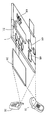
도 1은 광전 모듈의 단면도이다.
도 2는 도 1의 모듈의 구성요소의 다양한 단면도를 도시한다.
도 3은 도 1에 도시된 바와 같은 다중 모듈을 제조하기 위한 웨이퍼 스택을 형성하기 위한 웨이퍼의 단면도이다.
도 4는 도 1의 다중 모듈을 제조하기 위한 웨이퍼 스택의 단면도이다.
도 5는 구조화된 표면을 갖는 반제품의 단면도이다.
도 6은 광 근접 센서를 갖는 모바일 폰의 예를 예시한다.
도 7은 모바일 폰의 추가 상세사항을 예시한다. 1 is a sectional view of a photoelectric module.
Figure 2 shows various cross-sectional views of the components of the module of Figure 1;
3 is a cross-sectional view of a wafer for forming a wafer stack for manufacturing multiple modules as shown in FIG.
Figure 4 is a cross-sectional view of the wafer stack for making the multiple modules of Figure 1;
5 is a cross-sectional view of a semi-finished product having a structured surface.
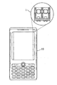
Figure 6 illustrates an example of a mobile phone having an optical proximity sensor.
Figure 7 illustrates additional details of a mobile phone.
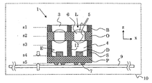
도 1에 예시한 바와 같이, 광전 모듈(1)은 적어도 하나의 능동 광 컴포넌트 및 적어도 하나의 수동 광 컴포넌트를 포함할 수 있다. 능동 광 컴포넌트의 예는, 광 다이오드, 이미지 센서, LED, OLED 또는 레이저 칩과 같은 광 감지 또는 발광 컴포넌트를 포함한다. 수동 광 컴포넌트의 예는, 렌즈, 프리즘, 미러 또는 광 시스템(예를 들어, 구경 조리개, 이미지 스크린 또는 홀더와 같은 기계적 요소를 포함할 수 있는 수동 광 컴포넌트의 집합)과 같은, 굴절 및/또는 회절 및/또는 반사에 의해 광을 재전송하는 광 컴포넌트를 포함한다. 도 2는 도 1의 모듈의 구성요소의 다양한 횡 방향 개략 단면도를 도시하며, 상기 횡 방향 단면의 대략적인 위치는 도 1에서 s1 내지 s5 및 파선으로 나타낸다. s4 및 s5에 있어서, 보는 방향을 화살표로 나타낸다.As illustrated in FIG. 1, the
모듈(1)은 종 방향(즉, 도 1의 z 방향)으로 서로 위에 적층된 여러 개의 구성요소(P,S,O,B)를 포함한다. 종(z) 방향에 수직인 x-y 면(도 2 참조) 방향을 횡방향으로 지칭할 수 있다.The
모듈(1)은 서로 위에 적층된, 기판(P), 분리 부재(S), 광학 부재(O) 및 배플 부재(baffle member)(B)를 포함한다. 기판(P)은, 예를 들어 인쇄 회로 기판 조립체이다. PCB 조립체의 인쇄 회로 기판(PCB)은 인터포저로 지칭할 수 있다. PCB 상에는 광 방출을 위한 방출 부재(E)(예를 들어, 적외선 광 또는 근적외선 광 방출을 위한 발광 다이오드를 포함하는 광 송신기 다이), 및 방출 부재(E)에 의해 방출된 주파수/파장(또는 주파수들/파장들 범위)의 광을 검출하기 위한 검출 부재(D)(예를 들어, 적외선 광 또는 근적외선 광 검출을 위한 광 다이오드를 포함하는 광 수신기 다이)가 실장된다. 일반적으로, 광은 전자기 방사를 지칭하며, 예를 들어 전자기 스펙트럼의 적외선, 가시광선 또는 자외선 부분의 전자기 방사를 포함할 수 있다.The
방출 부재(E) 및 검출 부재(D)의 전기 콘택트는 납땜 볼(7)이 부착된 모듈(1) 외부에 전기적으로 접속된다. 일부 구현은 4개의 전기 콘택트를 포함하며; 2개는 방출 부재(E)용이고 2개는 검출 부재(D)용이다. 납땜 볼(7)을 제공하는 대신에, 일부 구현은 이후에 납땜 볼이 제공될 수 있는 PCB 상의 콘택 패드를 포함한다. 따라서 모듈(1)은 예를 들어 표면 실장 기술(surface mount technology;SMT)을 이용하여 다른 전자 컴포넌트 옆에, 인쇄 회로 기판(9)상에 실장될 수 있다. 인쇄 회로 기판(9)은 핸드헬드 통신 장치와 같은 전자 장치(10)의 구성요소일 수 있다. 예를 들어, 장치(10)는 스마트폰 또는 다른 모바일 폰일 수 있다. 모듈(1)은 특히 작은 크기를 갖도록 제조될 수 있으므로 상기 응용에 특히 적합하다.The electrical contacts of the emitting member E and the detecting member D are electrically connected to the outside of the
분리 부재(S)는 2개의 개구부(4)를 가지며, 이들 중 하나에 방출 부재(E)가 배치되고 다른 하나에 검출 부재(D)가 배치된다. 이러한 방식으로, 방출 부재(E) 및 검출 부재(D)는 분리 부재(S)에 의해 횡 방향으로 둘러싸인다. 비록 개구부는 실질적으로 원형으로 도시되지만, 일부 구현에서는 다른 형상을 가질 수 있다.The separating member S has two
분리 부재(S)는 몇 가지 임무를 수행할 수 있다. 이는 기판(P)과 광학 부재(O) 사이에 명확한 거리를 보장할 수 있으며(그의 수직 연장부를 통해), 이는 방출 부재(E)로부터 광학 부재(O)를 통해, 및 모듈(1) 외부로부터 광학 부재(O)를 통해 검출 부재(D) 상으로의 명확한 광 경로를 달성하는 것을 돕는다. 분리 부재(S)는 또한, 검출 부재(D)에 의해 대체적으로 검출가능한 광에 실질적으로 불투명하고 모듈(1)의 외부 벽의 일부를 형성함으로써, 검출 부재(D)에 의해 검출되지 않아야 하는 광으로부터 검출 부재(D)를 보호할 수 있다. 분리 부재(S)는 또한, 검출 부재(D)에 의해 대체적으로 검출가능한 광에 실질적으로 불투명하고 방출 부재(E)와 검출 부재(D) 사이에 벽을 형성함으로써, 방출 부재(E)와 검출 부재(D) 간의 광 크로스토크를 감소시키도록, 검출 부재(D)에 도달하지 않아야 하는 방출 부재(E)에 의해 방출된 광으로부터 검출 부재(D)를 보호할 수 있다. 상기 방식으로, 모듈(1) 내부에 반사된 광 및 방출 부재(E)로부터 유래한 미광(stray light)이 검출 부재(D)에 도달하지 못하도록 할 수 있다. 일부 구현에서, 분리 부재(S)는 불투명 중합체 재료, 예를 들어 에폭시 수지, 아크릴레이트, 폴리우레탄, 실리콘 재료와 같은 굳어질 수 있는(예를 들어, 경화성) 중합체 재료로 제조된다. 분리 부재는, 예를 들어 카본 블랙을 포함하는 경화성 중합체로 제조될 수 있다.The separating member S can perform several tasks. This can ensure a clear distance between the substrate P and the optical member O (through its vertical extension), which is transmitted from the emitting member E through the optical member O and from the outside of the
최대 감도 및 검출 범위를 달성하기 위해, 방출 부재(예를 들어, LED)(E)와 검출 부재(예를 들어, 광 다이오드)(D) 간의 근거리(close distance)가 중요할 수 있다. 하지만, 잘못된 센서 반응을 방지하고 내부 크로스토크로 인한 동적 범위의 감소를 방지하기 위해, 수신기 가까이에 위치한 방출기는 분리 벽 또는 커버에 의한 IR-유효 광 절연을 필요로 한다. 분리 부재(S)는 방출 부재(E)와 검출 부재(D)를 서로 분리하여 내부 광 크로스토크를 감소시키는 것을 도울 수 있는 수직 벽 분할 부(12)를 갖는다.A close distance between the emitting member (e.g. LED) E and the detecting member (e.g., photodiode) D may be important to achieve maximum sensitivity and detection range. However, in order to prevent false sensor response and prevent the dynamic range from decreasing due to internal crosstalk, the emitter located near the receiver requires IR-effective optical isolation by a separating wall or cover. The separating member S has a vertical
광학 부재(O)는 차단 부(b) 및 2개의 투명 부(t)를 포함하며, 2개의 투명 부(t) 중 하나는 방출 부재(E)에 의해 방출된 광이 모듈(1)을 나갈 수 있도록 하기 위한 것이고, 다른 하나는 광이 모듈(1)의 외부로부터 모듈(1)에 들어와 검출 부재(D)에 도달할 수 있도록 하기 위한 것이다.The optical member O comprises a blocking portion b and two transparent portions t wherein one of the two transparent portions t allows the light emitted by the emitting member E to exit the
차단 부(b)는, 예를 들어 적절한 (중합체) 재료로 제조함으로써, 검출 부재(D)에 의해 대체적으로 검출가능한 광에 대해 실질적으로 불투명하다. 투명 부(t)는 수동 광학 컴포넌트(L)를 포함하거나, 더 구체적으로 및 예로서, 광 가이드를 위한 렌즈 부재(L)를 각각 포함한다. 렌즈 부재(L)는, 예를 들어, 도 1에 도시한 바와 같이, 투명 요소(6)에 밀접하게 접한 2개의 렌즈 요소(5)를 포함할 수 있다. 투명 요소(6)는, 차단 부(b)를 형성하는 광학 부재(O)가 투명 요소(6)와 함께 (완벽에 가까운) 완전한 플레이트 형상을 제공하도록, 차단 부(b)를 형성하는 광학 부재(O)와 동일한 종 방향 치수를 가질 수 있다. 렌즈 요소(5)(도 1 참조)는 굴절 및/또는 회절에 의해 광을 리디렉트(redirect)한다. 예를 들어, 렌즈 요소는 모두 대체적으로 볼록한 형상(도 1에 도시된 바와 같이)일 수 있지만, 렌즈 요소(5)의 하나 이상은 다른 형상일 수 있으며, 예를 들어 대체적으로 또는 부분적으로 오목할 수 있다.The blocking portion (b) is substantially opaque to light generally detectable by the detecting member (D), for example, by being made of a suitable (polymer) material. The transparent portion t comprises a passive optical component L or, more specifically and as an example, comprises a lens element L for a light guide, respectively. The lens element L may comprise, for example, two
배플 부재(B)는 원치 않는 광, 특히 원하는 각도로 모듈(1)을 나가거나 모듈(1)에 입사하는 광을 차폐할 수 있다. 배플 부재(B)는 개구부로서 또는 투명 재료에 의해 형성될 수 있는 2개의 별도 투명 구역(3)을 가질 수 있다. 투명 구역(3) 외부의 배플 부재(B)는 검출 부재에 의해 대체적으로 검출가능한 광을 실질적으로 약화시키거나 차단하는 재료로 제조될 수 있거나, 비록 제조하기가 더 복잡할 수 있기는 하지만 상기 특성을 갖는 코팅이 제공될 수 있다. 배플 부재(B)의 형상, 또는 더욱 정확하게는 투명 구역(3)의 형상은 도 1 및 2에 도시된 것과 상이할 수 있다(예를 들어, 원뿔형 또는 각뿔대).The baffle member B can shield unwanted light, particularly light exiting the
투명 구역(3)뿐만 아니라 투명 부(t) 및 개구부(4)의 횡 방향 형상은 원형일 필요가 없으며 다른 형상, 예를 들어 다각형 또는 둥근 모서리를 갖는 직사각형일 수 있다.The lateral shape of the transparent portion (t) and the opening portion (4) as well as the transparent portion (3) need not be circular but may be a rectangle having a different shape, for example a polygon or a rounded edge.
모듈(1)은 패키징된 광전 컴포넌트이다. 모듈(1)의 수직 측벽은 아이템 P, S, O 및 B로 형성된다. 하부 벽은 기판(P)으로 형성되고, 상부 벽은 배플 부재(B), 또는 광학 부재(O)와 함께 배플 부재(B)로 형성된다.
도 2에 도시된 바와 같이, 하우징 컴포넌트로도 지칭될 수 있는 4개의 아이템 P, S, O, B는 각각 다른 하우징 컴포넌트와 실질적으로 동일한 횡 방향 형상 및 횡 방향 치수를 갖는다. 이는 하기에 도 3 및 4를 참조로 더 상세히 설명한 바와 같이, 상기 모듈(1)을 매우 효율적인 방식으로 제조하는 것을 용이하게 한다. 각각의 하우징 컴포넌트(P, S, O 및 B)는 대체적으로 블럭 또는 플레이트 유사 형상을 가지거나, 더 일반적으로, 가능하게는 홀 또는 개구부(배플 부재(B) 및 분리 부재(S)가 갖는 것과 같은) 또는 돌출부(광학 부재(O)가 갖는 것과 같은)를 갖는, 직사각형의 평행 육면체 형상을 갖는다.As shown in Figure 2, the four items P, S, O, B, which may also be referred to as housing components, each have substantially the same transverse and transverse dimensions as the other housing components. This facilitates manufacturing the
일부 구현에서, 모듈(1)은 근접 센서이다. 상기 모듈(1)에 의해, 방출 부재(E)가 예를 들어 광 펄스의 형태로 광을 방출하는 동안, 예를 들어 검출 부재(D)에 의해 생성된 광전류로부터 판단하여, 모듈로부터의 사전 정의된 거리 이내에 대상물이 위치하는지 여부를 검출할 수 있다. 예를 들어, 방출 부재(E), 광학 부재(O) 및 검출 부재(D)는, 광학 부재(O)의 사전 정의된 거리 또는 거리 범위 이내에 위치한 광을 반사할 수 있는 표면이, 방출 부재(E)에 의해 방출되고 상기 표면에 의해 반사된 충분히 높은 강도의 광을 검출 부재(D)에 의해 검출가능하도록 하는 반면, 방출 부재(E)에 의해 방출되고 광학 부재(O)로부터 더 멀리 떨어져 위치하고 상기 사전 정의된 거리 바깥에 위치한 표면에 의해 반사된 광은 각각, 검출 부재(D)에 의해 충분히 높은 광 강도가 검출되지 않게 하도록 배치될 수 있다.In some implementations,
또한, 검출 부재(D)에 추가하여, 추가 광 검출기와 같은 하나 이상의 추가 전자 컴포넌트, 또는 하나 이상의 집적 회로, 또는 2개 이상의 광원을 포함하는 것을 제외하고는 상술한 것과 동일한 원리에 따라 설계된 모듈을 제공하는 것이 가능하다.Further, in addition to the detecting member D, a module designed according to the same principle as described above, except that it includes one or more additional electronic components such as additional photodetectors, or one or more integrated circuits, or two or more light sources, It is possible to provide.
모듈(1)의 능동 전자 컴포넌트(예를 들어, 도 1의 예의 방출 부재(E) 및 검출 부재(D))는 패키징된 또는 패키징되지 않은 전자 컴포넌트일 수 있다. 기판(P)과 접촉시키기 위해, 와이어-본딩 또는 플립 칩 기술과 같은 기술, 또는 종래의 쓰루-홀 기술에서 사용하는 것과 같은 다른 임의의 공지된 표면 실장 기술을 사용할 수 있다.The active electronic components of module 1 (e. G., Emissive element E and detector element D in the example of FIG. 1) may be packaged or unpackaged electronic components. Any other known surface mounting technique, such as used in wire-bonding or flip-chip technology, or in conventional through-hole technology, may be used to contact substrate P
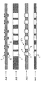
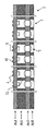
도 3은 도 1에 도시된 바와 같은 다중 모듈을 제조하기 위한 웨이퍼 스택을 형성하기 위한 웨이퍼의 개략적인 단면도를 도시한다. 일반적으로, 웨이퍼는 실질적으로 디스크- 또는 플레이트-유사 형상 아이템을 지칭하며, 그의 한 방향(z-방향 또는 수직 방향)의 연장부는 다른 두 방향(x- 및 y-방향 또는 횡 방향)의 연장부에 비해 작다. (비어 있지 않은) 웨이퍼 상에는, 예를 들어 직사각형 그리드 상에 복수의 유사한 구조 또는 아이템이 배치되거나 그 안에 제공될 수 있다. 웨이퍼는 개구부 또는 홀을 가질 수 있으며, 일부 경우에 웨이퍼는 횡 방향 영역의 대다수 부분에 재료가 없을 수 있다. 구현에 따라, 웨이퍼는 예를 들어 반도체 재료, 중합체 재료, 금속 및 중합체, 또는 중합체 및 유리 재료를 포함하는 복합 재료로 제조될 수 있다. 특히, 웨이퍼는 열-경화성 또는 UV-경화성 중합체와 같은 굳어질 수 있는 재료를 포함할 수 있다. 일부 구현에서, 웨이퍼의 직경은 5 cm와 40 cm 사이이고, 예를 들어 10 cm와 31 cm 사이일 수 있다. 웨이퍼는 예를 들어 직경이 2,4,6,8 또는 12 인치(1인치는 약 2.54 cm임)인 원통형일 수 있다. 웨이퍼 두께는 예를 들어 0.2 mm와 10 mm 사이일 수 있으며, 일부 경우에 0.4 mm와 6 mm 사이이다.3 shows a schematic cross-sectional view of a wafer for forming a wafer stack for manufacturing multiple modules as shown in Fig. Generally, a wafer refers to a substantially disk-like or plate-like shaped item, and an extension in one direction (z-direction or vertical direction) may extend in two different directions (x- and y- . (Not empty) wafer, a plurality of similar structures or items may be disposed or provided on, for example, a rectangular grid. The wafer may have openings or holes, and in some cases the wafer may be free of material in the majority of the lateral region. Depending on the implementation, the wafer may be made of, for example, a semiconductor material, a polymeric material, a metal and a polymer, or a composite material comprising a polymer and a glass material. In particular, the wafer may comprise a hardenable material such as a heat-curable or UV-curable polymer. In some implementations, the diameter of the wafer is between 5 cm and 40 cm, for example between 10 cm and 31 cm. The wafer may be cylindrical, for example, having diameters of 2, 4, 6, 8 or 12 inches (one inch is about 2.54 cm). The wafer thickness may for example be between 0.2 mm and 10 mm, in some cases between 0.4 mm and 6 mm.
비록 도 3 및 4는 3개의 모듈(1)에 대한 경우만을 도시하지만, 일부 구현에서는, 하나의 웨이퍼 스택에 각 횡 방향에 적어도 10개의 모듈의 경우가 존재할 수 있으며, 일부 경우에는, 각 횡 방향에 적어도 30개 또는 심지어 50개 이상의 모듈의 경우가 존재할 수 있다. 각 웨이퍼의 치수의 예는: 횡 방향으로 적어도 5 cm 또는 10 cm, 및 30 cm 또는 40 cm 또는 심지어 50 cm 까지고; 종 방향으로(기판 웨이퍼(PW) 상에 컴포넌트들을 배치하지 않고 측정) 적어도 0.2 mm 또는 0.4 mm 또는 심지어 1 mm이며, 6 mm 또는 10 mm 또는 심지어 20 mm 까지다.Although Figures 3 and 4 illustrate only three
일부 구현에서, 도 1에 도시된 다중 모듈을 제조하기 위한 웨이퍼 스택을 생성하기 위해 4개의 웨이퍼를 사용할 수 있다. 도 4에 도시된 바와 같이, 스택은 기판 웨이퍼(PW), 스페이서 웨이퍼(SW), 광학 웨이퍼(OW) 및 배플 웨이퍼(BW)를 포함한다. 각 웨이퍼는, 예를 들어 직사각형 격자 상에 배치되고 이후의 분리 단계를 용이하게 하기 위해 서로 약간의 거리를 갖는, 상응하는 모듈(1)(도 1 및 2 참조)에 포함된 다수의 상응하는 부재들을 포함한다. In some implementations, four wafers may be used to create a wafer stack for manufacturing the multiple modules shown in FIG. As shown in Fig. 4, the stack includes a substrate wafer PW, a spacer wafer SW, an optical wafer OW, and a baffle wafer BW. Each of the wafers may include a plurality of corresponding members (not shown) included in the corresponding module 1 (see Figs. 1 and 2), for example, arranged on a rectangular grid and having a slight distance from each other to facilitate subsequent separation steps .
기판 웨이퍼(PW)는, 예를 들어 한 측 상에 납땜 볼(7)이 제공되고 다른 측에 능동 광 컴포넌트(예를 들어, 부재 E 및 D)가 땜납된, 표준 PCB 재료의 PCB를 포함하는 PCB 조립체일 수 있다. 능동 광 컴포넌트는 예를 들어, 표준 픽앤플레이스 기계를 이용하여 픽앤플레이스에 의해 기판 웨이퍼(PW) 상에 배치될 수 있다.The substrate wafer PW comprises a PCB of a standard PCB material, for
스페이서 웨이퍼(SW)는 기판 웨이퍼(PW) 및 광학 웨이퍼(OW)가 서로 실질적으로 일정한 거리로 유지되는 것을 도울 수 있다. 따라서, 웨이퍼 스택에 스페이서 웨이퍼(SW)를 포함시킴으로써 더 높은 영상 성능 및 복잡성(complexity)을 가능하게 할 수 있다. 적층된 웨이퍼는 이후에 개별 마이크로 광학 구조로 다이싱(diced)될 수 있어서, 웨이퍼당 복수의(예를 들어, 수천 개의) 구조체를 초래할 수 있다.The spacer wafer SW can help the substrate wafer PW and the optical wafer OW to be maintained at a substantially constant distance from each other. Thus, by including a spacer wafer SW in the wafer stack, higher image performance and complexity can be enabled. The stacked wafers can then be diced into individual micro-optical structures, resulting in multiple (e.g., thousands) structures per wafer.
원치 않는 광을 검출하는 것을 최대한 방지하기 위해, 각각의 웨이퍼(PW, SW, OW, BW)는 투명 부(t) 및 투명 구역(3)과 같은 투명 영역을 제외하고, 검출 부재(D)에 의해 검출가능한 광에 대해 실질적으로 불투명한 재료로 실질적으로 제조될 수 있다.Each of the wafers PW, SW, OW and BW is formed on the detection member D except for the transparent region such as the transparent region t and the
예를 들어, 일부 구현에서, 스페이서 웨이퍼(SW)는 카본 블랙 또는 다른 어두운 안료를 포함하는 UV- 또는 열-경화성 에폭시(또는 다른 중합체)로 제조될 수 있다. 일부 구현에서, 카본 블랙은 에폭시(또는 다른 중합체)에 매립된다. 에폭시 또는 다른 중합체 재료에서 카본 블랙의 양은 특정 응용에 따라 달라질 수 있고, 예를 들어 스페이서 웨이퍼(SW)의 원하거나 요구되는 광 특성에 따라 달라질 수 있다. 따라서, 일부 구현에서, 광 크로스토크, 또는 검출 부재(D)에 의한 다른 바람직하지 않은 광의 검출을 감소시키기 위해, 스페이서 웨이퍼(SW)는, 비록 일부 구현에서는 더 적은 양의 카본 블랙이 충분할 수도 있지만, 적어도 0.7%의 카본 블랙을 포함하는 UV 또는 열 경화성 에폭시 또는 다른 중합체 재료로 제조될 수 있다. 스페이서 웨이퍼(SW)용 에폭시 또는 다른 중합체 재료에서 카본 블랙의 최적 또는 원하는 퍼센트는, 예를 들어 벽(12)의 횡 방향 두께에 따라 조정될 수 있다. 예를 들어, 일부 구현에서, 벽 두께는 약 200 ㎛이고, 에폭시 재료 또는 다른 중합체 재료는 약 적어도 0.8%의 카본 블랙을 포함한다. 파장이 800 nm인 광에 있어서, 상기 조성은 약 0.0295/㎛의 흡수 계수(α)를 초래할 수 있다. 일반적으로, 두께(d)를 갖는 벽 부분(12)의 투과율(T)은 10-α*d이다. 따라서, 상기 예에서, 벽 부분(12)을 통한 투과율(T)은 0.00015% 미만이며, 이는 약 5.8의 흡수율 또는 광 밀도에 상응하며, 흡수율은 재료를 통해 전달되는 방사량에 대한 재료상에 쏟아지는 방사량의 대수 비율을 나타낸다. 일부 응용에서, 카본 블랙의 양은 방출 부재(E)에 의해 방출된 광의 파장에서 벽 부분(12)을 통과한 광의 투과율(T)이 0.1% 이하이도록 충분히 많다. 유사하게, 일부 응용에서, 카본 블랙의 양은 방출 부재(E)에 의해 방출된 광의 파장에서 벽 부분(12)의 흡수율 또는 광 밀도가 적어도 3 이도록 충분히 많다. 일부 구현에서, 분리 부재(S)는 벽(12)의 두께가 약 200 ㎛인 경우 광 방출기에 의해 방출된 광의 파장에서 적어도 0.015/㎛의 흡수 계수(α)를 갖는다.For example, in some implementations, the spacer wafer SW may be made of a UV- or heat-curable epoxy (or other polymer) comprising carbon black or other dark pigment. In some implementations, the carbon black is embedded in an epoxy (or other polymer). The amount of carbon black in the epoxy or other polymeric material may vary depending on the particular application, for example, depending on the desired or desired optical properties of the spacer wafer SW. Thus, in some implementations, to reduce detection of optical crosstalk, or other undesirable light by the detecting member D, the spacer wafer SW may have a smaller amount of carbon black , ≪ / RTI > at least 0.7% carbon black, or other polymeric materials. The optimum or desired percentage of carbon black in the epoxy or other polymeric material for the spacer wafer (SW) can be adjusted, for example, in accordance with the lateral thickness of the
해당되는 파장(들)(즉, LED 또는 다른 방출 부재(E)에 의해 방출된 광의 파장(들))에서 스페이서 웨이퍼의 광 전송 특성을 감소시키기 위해 하나 이상의 안료 또는 다른 첨가제를 첨가하여, 스페이서 웨이퍼(SW)용 기재 재료로서 다양한 중합체 재료(예를 들어, 에폭시 수지, 아크릴레이트, 폴리우레탄 또는 실리콘 재료)를 사용할 수 있다. 스페이서 웨이퍼(SW)용 기재 재료의 예는 하기 중 하나 이상을 포함한다: Electronic Materials, Inc.제 EMCASTTM(예를 들어, 23xx, 24xx, 25xx 및 2600 시리즈); Master Bond Inc.제 MASTERBONDTM(예를 들어, UV15-7DC, UV1ODCTK); DELO Industrial Adhesives제 DELO-DUALBONDTM(예를 들어, AD VE 80342); Addison Clear Wave제 AC A1449; Epoxy Technology, Inc.제 EPOTEK OG198-54; 및 LOCTITE 334,392,5091. 상기 재료 중 일부는 이중 경화된다(즉, UV 광에 의해서뿐만 아니라 열적으로 경화될 수 있음). 해당되는 파장(들)에서 스페이서 웨이퍼(SW)의 광 전송 특성을 감소시키기 위해 기재 재료에 카본 블랙 또는 다른 안료를 첨가할 수 있다. 예를 들어, 방출 부재(E)에 의해 방출된 광의 파장에서 벽 부분(12)을 통과한 광의 투과율(T)이 0.1% 이하 이도록 충분히 많은 양의 카본 블랙 또는 다른 안료를 기재 중합체 재료에 첨가할 수 있다. 유사하게, 일부 응용에서, 방출 부재(E)에 의해 방출된 광의 파장에서 벽 부분(12)의 흡수율 또는 광 밀도가 적어도 3 이도록 안료의 양이 충분히 많다.One or more pigments or other additives may be added to reduce the light transmission characteristics of the spacer wafer at the corresponding wavelength (s) (i.e., the wavelength (s) of light emitted by the LED or other emissive element E) (For example, an epoxy resin, an acrylate, a polyurethane or a silicone material) may be used as the base material for the SW. Examples of substrate materials for spacer wafers (SW) include one or more of the following: EMCAST TM from Electronic Materials, Inc. (e.g., 23xx, 24xx, 25xx and 2600 series); MASTERBOND TM from Master Bond Inc. (e.g., UV15-7DC, UV1ODCTK); DELO Industrial Adhesives DELO-DUALBOND TM (for example AD VE 80342); Addison Clear Wave AC A1449; Epoxy Technology, Inc. EPOTEK OG198-54; And LOCTITE 334,392,5091. Some of these materials are double cured (i.e., can be thermally cured as well as by UV light). Carbon black or other pigments may be added to the substrate material to reduce the light transmission characteristics of the spacer wafer (SW) at the wavelength (s) of interest. For example, a sufficiently large amount of carbon black or other pigment may be added to the base polymeric material such that the transmittance (T) of the light passing through the
스페이서 웨이퍼(SW) 및 배플 웨이퍼(BW)뿐만 아니라 광학 웨이퍼(OW)의 적어도 일부는, 예를 들어 복제에 의해 제조될 수 있다. 복제는 예를 들어 식각, 엠보싱(embossing), 몰딩(molding) 또는 진공 사출을 이용하여 주어진 구조 또는 그의 음의 구조(negative)가 재생되는 기술을 지칭한다. 복제 공정의 특정 예에서, 구조화된 표면을 액체의, 점성의 또는 소성변형가능한 재료에 엠보싱한 다음, 예를 들어 UV 방사 또는 가열을 이용하여 경화함으로써 재료를 굳어지게 하고, 이어서 구조화된 표면을 제거한다. 따라서, 구조화된 표면의 복제품(이 경우 음의 복제품)이 수득된다. 복제를 위한 적절한 재료는, 예를 들어 굳어지게 할 수 있는(예를 들어, 경화성) 중합체 재료 또는 다른 복제 재료이며, 즉 액체의, 점성의 또는 소성변형가능한 상태에서 고체 상태로의 굳어지는 단계 또는 고화 단계(예를 들어, 경화 단계)에서 변형가능한 재료이다.At least a part of the spacer wafer SW and the baffle wafer BW as well as the optical wafer OW can be produced by, for example, replication. Cloning refers to techniques in which a given structure or its negative structure is reproduced, for example, using etching, embossing, molding or vacuum injection. In a specific example of a replication process, the structured surface is embossed into a liquid, viscous or plastic deformable material, followed by curing using, for example, UV radiation or heating to harden the material, followed by removal of the structured surface do. Thus, a clone of the structured surface (in this case a negative clone) is obtained. Suitable materials for replication are, for example, polymeric materials or other replication materials that can be hardened (e.g., curable), i.e., solidified into a solid state from a viscous or plastic deformable state of the liquid, Is a deformable material in the solidification step (e.g., curing step).
따라서, 웨이퍼-레벨 복제 공정은, 예를 들어 용도별 액체 중합체의 액적을 웨이퍼 상에 정확하게 분배함으로써 구현될 수 있다. 이어서, 몰드를 이용하여 중합체를 엠보싱하고 UV 광을 이용하여 웨이퍼 상에서 경화시켜 이를 굳어지게 한다. 이어서, 웨이퍼를 몰드에서 분리한다. 마이크로미터의 정렬 정확도로 웨이퍼의 다른 측 상에서 상기 공정을 반복할 수 있다. 일부 구현에서, 본 출원에 참조로 포함된 미국 특허 제7,704,418호에 설명된 바와 같이, 기판의 표면과 기구 사이에 복제 재료를 가둘 수 있다.Thus, the wafer-level duplication process can be implemented, for example, by accurately dispensing droplets of the application-specific liquid polymer onto the wafer. The polymer is then embossed using a mold and cured on the wafer using UV light to harden it. Then, the wafer is separated from the mold. The process can be repeated on the other side of the wafer with micrometer alignment accuracy. In some implementations, replication material may be confined between the surface of the substrate and the device, as described in U.S. Patent No. 7,704,418, which is incorporated herein by reference.
스페이서 웨이퍼(SW)를 제조하기 위한 적절한 복제 기술은 예를 들어, 둘 모두 본 출원에 참조로 포함된, 미국 특허공개 제2011/0039048 A1호 및 미국 가출원 제61/746,347호에 개시된다. 스페이서 웨이퍼(SW)는 에지의 두께가 에지 주변의 표면 위치에서의 스페이서 웨이퍼의 두께를 초과하도록 제조될 수 있다. 이 방식으로, 에지는 스페이서의 평균 두께에 비해 높다. 예를 들어, 스페이서 웨이퍼(SW) 자체가 통상적으로 100 내지 1500 ㎛의 두께를 가질 경우, 둘러싼 표면에 대한 에지의 높이는 약 1-10 ㎛일 수 있다.Suitable replication techniques for making spacer wafers (SW) are disclosed, for example, in U.S. Patent Application Publication No. US 2011/0039048 A1 and U.S. Provisional Patent Application Serial No. 61 / 746,347 both of which are incorporated herein by reference. The spacer wafer SW can be manufactured such that the thickness of the edge exceeds the thickness of the spacer wafer at the surface position around the edge. In this way, the edge is higher than the average thickness of the spacer. For example, if the spacer wafer SW itself normally has a thickness of 100 to 1500 [mu] m, the height of the edge to the surrounding surface may be about 1-10 [mu] m.
일부 구현에서, 웨이퍼-레벨 경화 공정을 통과한 복제 요소들(예를 들어, 스페이서 웨이퍼(SW), 광학 웨이퍼(OW) 및 기판 웨이퍼(PW))은 열적으로 안정하며, 온도가 예를 들어 약 260 ℃까지 도달할 수 있는 리플로우 공정과 같은 열 공정을 견딜 수 있다. 열적으로 안정한 요소들은 그들의 대체적인 형상을 실질적으로 유지하며 비교적 높은 작동 온도에서 분해되지 않는다. 이러한 복제 요소들의 특성을 일반적으로 "리플로우성"으로 지칭한다. 열적으로 안정한 요소들을 제조하기 위해 사용된 재료는 예를 들어, 열경화성 중합체 또는 열가소성 중합체를 포함할 수 있다.In some implementations, the replicate elements (e.g., spacer wafer SW, optical wafer OW, and substrate wafer PW) that have passed through the wafer-level curing process are thermally stable, It can withstand a thermal process such as a reflow process that can reach up to 260 ° C. The thermally stable elements substantially retain their alternate shape and are not degraded at relatively high operating temperatures. The nature of such replicating elements is generally referred to as "reflow ". The materials used to make the thermally stable elements can include, for example, thermosetting polymers or thermoplastic polymers.
상기 제조 기술은, 모듈이 조립 라인 공정에 바로 통합될 수 있으므로, 예를 들어 모바일 폰 또는 다른 전자 제품에 모듈이 포함되는 것을 용이하게 한다. 일부 구현에서, 리플로우 가능한 요소들은 -40 ℃와 +85 ℃ 사이에서 1000 회, 및 +85 ℃ 온도 및 85% 상대 습도에서 1000 시간의 열 사이클을 포함하는 GR-468 CORE 환경 테스트를 만족한다.Such manufacturing techniques facilitate the inclusion of the module in, for example, a mobile phone or other electronic product, since the module can be integrated directly into the assembly line process. In some implementations, the reflowable elements meet the GR-468 CORE environmental test, which includes 1000 cycles between -40 ° C and + 85 ° C, and 1000 hours of thermal cycling at +85 ° C temperature and 85% relative humidity.
예를 들어, 상술한 바와 같이, 스페이서 웨이퍼(SW)는, 일부 구현에서는 카본 블랙도 또한 포함하는, 에폭시 수지 및 경화제로 형성된 열경화성 에폭시일 수 있다. 상기 에폭시 화합물의 열 안정성은 주로 에폭시 수지의 화학적 구조 및 경화제의 종류에 좌우된다. 예를 들어, 열가소성 에폭시 화합물에 있어서, 에폭시 화합물의 유리 전이 온도는 약 100 내지 약 270 ℃의 범위 이내에서 변화할 수 있다.For example, as described above, the spacer wafer SW may be a thermosetting epoxy formed of an epoxy resin and a curing agent, which also includes carbon black in some implementations. The thermal stability of the epoxy compound depends mainly on the chemical structure of the epoxy resin and the type of curing agent. For example, for thermoplastic epoxy compounds, the glass transition temperature of the epoxy compound may vary within the range of about 100 to about 270 占 폚.
복제 요소들은 또한 열적으로 안정한 UV-경화성 에폭시 또는 다른 중합체 재료로 형성될 수 있다. 일부 구현에서, 복제 요소들은 "이중-경화성"인 재료를 이용하여 형성될 수 있다. 즉, 재료는 2개의 경화 방법 중 어느 것을 사용하는 지에 따라 열(열 경화성) 또는 UV 광(UV-경화성) 중 하나를 이용하여 경화될 수 있다. 열적으로 안정한 경화성 중합체에 사용될 수 있는 재료의 예는 하기 중 하나 이상을 포함한다: Electronic Materials, Inc제 EMCASTTM(예를 들어, 23xx, 24xx, 25xx 및 2600 시리즈); Master Bond Inc.제 MASTERBONDTM 에폭시(예를 들어, UV15-7DC 및 UV1ODCTK); DELO Industrial Adhesives제 DELO-DUALBONDTM(예를 들어, AD VE 80342) 재료; Addison Clear Wave제 AC A1449; Epoxy Technology, Inc제 EPOTEK OG198-54 에폭시; 및/또는 LOCTITE 334,392 및 5091 시리즈 재료.Replicating elements can also be formed from thermally stable UV-curable epoxy or other polymeric materials. In some implementations, the replicating elements may be formed using a material that is "dual-curable ". That is, the material may be cured using either heat (thermosetting) or UV light (UV-curing) depending on which of the two curing methods is used. Examples of materials that can be used for the thermally stable curable polymer include one or more of the following: EMCAST TM from Electronic Materials, Inc (e.g., 23xx, 24xx, 25xx and 2600 series); MASTERBOND TM by Master Bond Inc. Epoxy (e.g., UV15-7DC and UV1ODCTK); DELO Industrial Adhesives DELO-DUALBOND TM (e.g. AD VE 80342) material; Addison Clear Wave AC A1449; Epoxy Technology, Inc EPOTEK OG198-54 Epoxy; And / or LOCTITE 334,392 and 5091 series materials.
다른 재료의 예는 한정된 비율로 기능성 아미노 실란 및 아미노프로필메틸 디메틸 실록산 공중합체를 갖는 에폭시를 포함한다. 일부 구현에서 경화성 에폭시에 실리콘 화합물을 사용함으로써, 에폭시의 열 안정성, 화학적 저항성 및 내식성을 향상시킬 수 있는 한편, 트리메톡시기를 포함하는 실란을 사용하면 더 우수한 접착성을 제공할 수 있다.Examples of other materials include epoxies having functional aminosilanes and aminopropylmethyldimethylsiloxane copolymers in defined proportions. By using a silicone compound in the curable epoxy in some implementations, thermal stability, chemical resistance, and corrosion resistance of the epoxy can be improved, while using a silane containing a trimethoxy group can provide better adhesion.
이와 달리 또는 추가하여, 경화성 에폭시 또는 다른 중합체의 열 안정성은 경화제로서 환상 화합물을 사용함으로써 향상시킬 수 있다. 예를 들어, 비스페놀 A로 제조된 에폭시 수지의 열 안정성은 특히, 방향족 아민 및 무수물, 노볼락, 비스말레이미드(예를 들어, 디-(p-말레이미도페닐)메탄) 및 이미다졸 유도체를 이용함으로써 향상될 수 있다. 열 안정성을 향상시키기 위해 추가의 수지 및 경화제 조합도 또한 사용할 수 있다.Alternatively or in addition, the thermal stability of the curable epoxy or other polymer may be improved by using cyclic compounds as curing agents. For example, the thermal stability of epoxy resins made with bisphenol A is particularly favored by the use of aromatic amines and anhydrides, novolaks, bismaleimides (e.g., di- (p-maleimidophenyl) methane) and imidazole derivatives . Additional resin and curing agent combinations may also be used to improve thermal stability.
렌즈(L)용 재료도 또한, 검출 부재(D)에 의해 검출가능한 광에 대해 투명한 적절한 리플로우 가능 재료로 제조될 수 있다. 스페이서 웨이퍼 요소와 유사하게, 렌즈(L)용으로 적절한 재료는, 예를 들어, 굳어지게 할 수 있는(예를 들어, 경화성) 중합체 재료, 또는 액체의, 점성의 또는 소성변형가능한 상태에서 고체 상태로의 굳어지게 하는(예를 들어, 경화) 단계에서 변형되는 재료를 포함할 수 있다. 일부 구현에서, 렌즈 재료의 경화는 중합체 재료에 열, UV 광 또는 화학 첨가제를 인가함으로써 달성된다. 카본 블랙을 제외하고, 스페이서 웨이퍼(SW), 광학 웨이퍼(OW) 또는 기판 웨이퍼(PW)를 제조하기 위해 사용된 동일한 중합체 재료를 렌즈 재료로서 사용할 수 있다. 렌즈를 형성하기 위해 사용될 수 있는 다른 중합체 재료는, 예를 들어 하기 중 하나 이상을 포함한다: ThreeBond Co.,Ltd제 THREEBONDTM 3078A, 3078B 또는 3078C 시리즈 에폭시; 각각 DELO Industrial Adhesives제인 DELO-KATIOBONDTM AD VE 18499 에폭시 및 DELO-PHOTOBONDTM 에폭시(예를 들어, GB368 및 19923 시리즈); EPOTEKTM 에폭시(예를 들어, 90-172-4, 90-174-3, 100-24-3 또는 OG142-13 시리즈 에폭시); Kyoritsu Chemical&Co.,Ltd.제 Kyoritsu XLM-C5 또는 XRC 9-2 시리즈 에폭시; Micro Resist Technology GmbH제 MRT OrmocompTM US-S4 에폭시; Showa Denko K.K.제 Showa DenkoTM SAS008L-P 에폭시; 및/또는 Wellomer Adhesive Technology제 WELLOMERTM 에폭시 DUV 764 에폭시.The material for the lens L may also be made of a suitable reflowable material which is transparent to light detectable by the detecting member D. [ Similar to the spacer wafer element, a suitable material for the lens L may be, for example, a polymeric material that can be hardened (e.g., curable), or a solid state in a viscous or plastic- (E. G., Curing) step to < / RTI > In some implementations, curing of the lens material is accomplished by applying heat, UV light, or chemical additives to the polymer material. Except for carbon black, the same polymer material used for producing the spacer wafer SW, the optical wafer OW or the substrate wafer PW can be used as the lens material. Other polymeric materials that may be used to form the lens include, for example, one or more of the following: THREEBOND TM 3078A, 3078B or 3078C series epoxy made by ThreeBond Co., Ltd; DELO Industrial Adhesives Jane DELO-KATIOBOND TM AD VE 18499 epoxy and DELO-PHOTOBOND TM epoxy (e.g. GB368 and 19923 series); EPOTEK TM Epoxy (e.g., 90-172-4, 90-174-3, 100-24-3 or OG142-13 series epoxy); Kyoritsu Chemical & Co., Ltd. Kyoritsu XLM-C5 or XRC 9-2 series epoxy; MRT Ormocomp TM US-S4 Epoxy made by Micro Resist Technology GmbH; Showa Denko KK Showa Denko TM SAS008L-P Epoxy; And / or WELLOMER TM Epoxy DUV 764 epoxy from Wellomer Adhesive Technology.
광학 웨이퍼(OW)에 있어서, 불투명 부분(예를 들어, 차단 부(b))을 수득하기 위해 복제 또는 몰딩을 이용할 수 있다. 드릴링 또는 식각에 의해 투명 부(t)가 존재할 예정인 홀을 제공하는 것도 가능하다. 이후에, 상기와 같이 수득된 전구체 웨이퍼에 렌즈 부재(L)를 제공하여 광학 웨이퍼(OW)를 생성한다. 이는 복제에 의해, 예를 들어 일원화된 부품으로서 렌즈 부재(L)를 형성함으로써 달성될 수 있다. 하지만, 렌즈 부재(L)는 또한, 투명 구역(3)이 정의되는 홀 내에 투명 요소(6)를 포함하는 웨이퍼인 반제품에서 시작하여 제조될 수도 있다. 이는, 각 렌즈 부재(L)가 적어도 하나의 정점(apex)을 만들고 상기 정점들이 광학 웨이퍼(OW)의 수직 단면 바깥에 위치할 경우 특히 유용할 수 있다. 상기 반제품은 투명 구역(3)에 웨이퍼를 관통하는 홀을 갖지 않으며 표면 파상(corrugations)이 거의 없거나 얕은 표면 파상만을 갖는 편평한 디스크-유사 웨이퍼일 수 있고, 상기 표면 파상은 통상적으로 오목하며, 즉 차단 부(b)에 의해 묘사되는 바와 같이 웨이퍼 표면 너머로 연장되지 않는다.In the optical wafer OW, copying or molding may be used to obtain an opaque portion (e.g., blocking portion b). It is also possible to provide a hole in which the transparent portion (t) is to be present by drilling or etching. Thereafter, the lens member L is provided on the precursor wafer obtained as described above to produce an optical wafer OW. This can be achieved by copying, for example, by forming the lens member L as an unified part. However, the lens element L may also be fabricated starting from the semi-finished product, which is a wafer that contains the
투명 부가 존재할 예정인 홀 또는 개구부를 갖는 편평한 전구체 웨이퍼(통상적으로 하나의 재료로 제조됨)에서 시작하여, 이어서 예를 들어 분배 공정을 이용하여 홀을 투명 재료로 채우고, 예를 들어, 플립-칩 기술 등에서 언더필(underfilling) 공정을 위해 사용된 것과 같은 디스펜서를 이용하여 전구체 웨이퍼의 홀을 하나씩 채우거나, 예를 들어 스퀴지 공정(예를 들어, 스크린 인쇄로부터 공지된 바와 같은) 또는 재료를 배출하는 수 개의 중공 니들(needles)을 갖는 디스펜서를 이용하여 한번에 수 개의 홀을 채워서, 상기와 같은 반제품을 수득할 수 있다. 분배 동안, 웨이퍼는, 예를 들어 실리콘으로 제조된 편평한 지지 플레이트 상에 배치될 수 있다. 분배된 재료에 기포 또는 캐비티가 형성되면 생성되는 렌즈 부재(L)의 광 특성이 열화되므로 이를 방지하도록 주의를 기울여야 한다. 예를 들어, 재료를 배출하는 중공 니들을 하기 에지에 근접하도록 적절히 가이드함으로써, 웨이퍼 및 아래의 지지 플레이트에 의해 형성된 에지(또는 상기 에지에 근접한 곳)에서 웨이퍼 재료의 습윤을 시작하는 방식으로 분배를 수행할 수 있다. 이후에, 분배된 재료를 예를 들어 열 또는 UV 방사에 의해 경화하여 굳어진 투명 재료를 수득한다.Starting with a flat precursor wafer (typically made of one material) having holes or openings in which a transparent portion is to be present, holes are then filled with the transparent material, for example using a dispensing process, (For example, as known from screen printing), or a plurality of nozzles for discharging the material, for example a squeegee process (e. G., As known from screen printing), using a dispenser such as that used for the underfilling process, The semi-finished product as described above can be obtained by filling several holes at a time using a dispenser having hollow needles. During dispensing, the wafer may be placed on a flat support plate made, for example, of silicon. Care should be taken to prevent the formation of bubbles or cavities in the dispensed material, as this will degrade the optical properties of the resulting lens element (L). For example, by properly guiding the hollow needles discharging the material close to the following edge, it is possible to distribute the wafer material in such a manner as to initiate the wetting of the wafer material at the edge (or near the edge) formed by the wafer and underlying support plate Can be performed. Thereafter, the dispensed material is cured, for example by heat or UV radiation, to obtain a hardened transparent material.
상기 방식으로 형성될 수 있는 볼록 반월판을 연마에 의해 편평하게 하여, 웨이퍼 두께로 조절된 평행한 표면을 갖는 투명 요소(6)를 수득할 수 있다. 이어서, 복제에 의해, 렌즈 요소(5)를 웨이퍼(OW)의 한 측 또는 양 측(상부 또는 하부 측)에 도포한다. 오목 반월판인 투명 요소의 경우, 복제가 이들 위에 이루어질 수 있으며, 도포된 복제 재료의 양은 상응하게 조절될 수 있다.The convex meniscus which can be formed in this manner can be flattened by polishing to obtain a
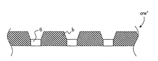
광학 웨이퍼(OW)뿐만 아니라 스페이서 웨이퍼(SW) 및/또는 배플 웨이퍼(BW)의 특징 및 기능을 포함하는 조합된 광학 웨이퍼를 제공하는 것이 가능하다. 상기 조합된 광학 웨이퍼의 제조는 특정 전구체 웨이퍼, 및 그 위를 기재로 제조된 특정 반제품을 이용하여 달성될 수 있다. 상기 전구체 웨이퍼 및 반제품은, 각각 전구체 웨이퍼에 제공되고 반제품에 존재하는 투명 요소의 2개 표면 중 적어도 하나 너머로 수직 연장된 돌출부를 통상적으로 갖는 적어도 하나의 구조화된 표면을 각각 갖는다. 도 5에서, 하나의 구조화된 표면을 갖는 반제품(ow')의 예를 개략적으로 예시한다. 반제품은 도 1에 도시된 모듈을 제조하기 위해 사용될 수 있다. 도 4의 웨이퍼 OW 및 SW(또는 웨이퍼 OW 및 BW, 또는 웨이퍼 OW 및 SW 및 BW)를 하나의 단일 부품으로서 간주함으로써, 도 1에 따른 모듈을 제조하기 위한 조합된 광학 웨이퍼가 제공된다.It is possible to provide a combined optical wafer including features and functions of the spacer wafer SW and / or the baffle wafer BW as well as the optical wafer OW. The fabrication of the combined optical wafer can be accomplished using specific precursor wafers, and certain semi-finished products made thereon. The precursor wafers and semi-finished products each have at least one structured surface, each typically provided with protrusions extending vertically over at least one of the two surfaces of the transparent element provided on the precursor wafer and present in the semi-finished product, respectively. In Figure 5, an example of a semi-finished product (ow ') having one structured surface is schematically illustrated. The semi-finished product can be used to manufacture the module shown in Fig. By considering the wafers OW and SW (or wafers OW and BW, or wafers OW and SW and BW) of Fig. 4 as one single component, a combined optical wafer for manufacturing the module according to Fig. 1 is provided.
웨이퍼 스택(2)을 형성하기 위해, 웨이퍼를 정렬하고, 예를 들어 열-경화성 및/또는 UV-경화성 에폭시 수지를 이용하여 예를 들어, 접착시킴으로써 웨이퍼를 함께 접합한다. 각 능동 광 컴포넌트(예를 들어, 기판 웨이퍼(PW) 상의 검출 부재(D) 및 방출 부재(E))는 상응하는 수동 광 컴포넌트(예를 들어, 광학 웨이퍼(OW)의 렌즈 부재(L))와 충분히 정확하게 정렬되어야 한다. 일부 구현에서, 기판 웨이퍼(PW)의 두께를 통해 연장된 홀을 기판 웨이퍼(PW)에 형성하여, 압력 형성(pressure build-up)을 해제시키기 위해 리플로우 공정 동안 환기시킬 수 있다. 홀은 드릴링 또는 식각 공정을 통해 기판 웨이퍼(PW)에 형성될 수 있다.To form the
도 4는 도 1에 도시된 바와 같은 다중 모듈(1)을 제조하기 위한 웨이퍼 스택(2)의 단면도를 도시한다. 가는 파선 직사각형은 예를 들어 다이싱 소(dicing saw)를 이용함으로써 분리가 발생하는 곳을 나타낸다.Fig. 4 shows a cross-sectional view of the
대부분의 정렬 단계가 웨이퍼 레벨에서 수행된다는 사실에 의해 비교적 간단하고 신속한 방식으로 양호한 정렬(특히 부재 L에 대한 부재 D 및 E의 정렬)을 달성하는 것이 가능하다. 따라서, 전반적인 제조 공정이 매우 신속하고 정확할 수 있다. 웨이퍼-규모 제조로 인해, 다중 모듈(1)을 제조하기 위해 적은 수의 제조 단계만이 요구된다.It is possible to achieve good alignment (particularly alignment of members D and E with respect to member L) in a relatively simple and fast manner by the fact that most alignment steps are performed at the wafer level. Thus, the overall manufacturing process can be very fast and accurate. Due to wafer-scale fabrication, only a few manufacturing steps are required to manufacture the
상술한 바와 같이, 일부 구현에서, 모듈(1)은 근접 센서 모듈이다. 상술한 기술에 의해, 웨이퍼-레벨 제조 공정을 이용하여 동시에 다중 모듈을 제조하는 것이 가능하다. 패키징된 모듈(1)은, 휴대용 전자 장치, 핸드헬드 휴대용 전자 장치, PC 장치, 카메라, 오디오 또는 비디오 재생 장치, 랩톱 컴퓨터 또는 PDA와 같은 광범위한 장치에 포함되고 작동가능하게 접속될 수 있다.As noted above, in some implementations,
근접 센서 모듈(1)의 특정 응용 예는 모바일 폰(10)(도 6 참조) 내에 존재하는 것이다. 예를 들어, 근접 센서 모듈(1)은 디스플레이가 사용되지 않을 경우 폰의 디스플레이를 자동으로 흐리게 하거나 비활성화하여 폰 배터리 수명을 연장할 수 있도록, 모바일 폰이 사용자의 귀 또는 얼굴 옆에 있는지를 감지하기 위해 사용될 수 있다. 도 7에 도시된 바와 같이, 모바일 폰(10)의 일부 구현은, 다른 컴포넌트 중에서도 특히 프로세서(52), 메모리(64), 디스플레이(54)와 같은 입출력 장치, 통신 인터페이스(66) 및 트랜시버(68)를 포함한다. 각종 버스를 이용하여 다양한 컴포넌트들이 상호접속될 수 있으며, 몇 개의 컴포넌트들은 공통 마더보드 상에 또는 다른 방식으로 적절히 실장될 수 있다. 근접 센서 모듈(1)은 또한 장치(10)의 다른 컴포넌트에 상호접속될 수 있으며, 일부 구현에서는 다른 컴포넌트들의 일부와 함께 공통 마더보드 상에 실장될 수 있다.A particular application of the
다수의 구현들을 설명하였다. 그럼에도 불구하고, 본 발명의 사상 및 범위로부터 벗어나지 않고 다양한 변형이 이루어질 수 있음이 이해될 것이다. 따라서, 다른 구현들은 청구항의 범위 이내이다.A number of implementations have been described. Nevertheless, it will be understood that various modifications may be made without departing from the spirit and scope of the invention. Accordingly, other implementations are within the scope of the claims.
Claims (36)
기판;
상기 기판의 제1면상에 실장된 광 방출기 - 상기 광 방출기는 제1 파장의 광을 방출하도록 작동가능함 -;
상기 기판의 제1면상에 실장된 광 검출기 - 상기 광 검출기는 상기 제1 파장의 광을 검출하도록 작동가능함 -;
상기 기판에 실질적으로 평행하게 배치된 광학 부재 - 상기 광학 부재는 상기 제1 파장의 광에 투명한 제1 및 제2 투명 부를 포함하고, 상기 광학 부재는 상기 제1 파장의 입사광을 실질적으로 약화시키거나 차단하는 차단 부를 더 포함하고, 상기 제1 투명 부는 상기 광 방출기 위에 배치되고 상기 제2 투명 부는 상기 광 검출기 위에 배치됨 -; 및
카본 블랙을 포함하는 불투명 중합체 재료로 구성된 분리 부재 - 상기 분리 부재는 상기 기판과 상기 광학 부재 사이에 이와 접촉하여 배치되고, 상기 분리 부재는 상기 광 방출기 및 상기 광 검출기를 둘러싸며, 상기 분리 부재는 상기 기판에서 상기 광학 부재까지 연장되고 상기 광 방출기와 상기 광 검출기를 서로 분리하는 벽 부분을 포함함 -
를 포함하는, 광 근접 센서 모듈.An optical proximity sensor module,
Board;
An optical emitter mounted on a first side of the substrate, the optical emitter operable to emit light of a first wavelength;
A photodetector mounted on a first side of the substrate, the photodetector operable to detect light of the first wavelength;
An optical member arranged substantially parallel to the substrate, wherein the optical member includes first and second transparent portions transparent to light of the first wavelength, and the optical member substantially weakens the incident light of the first wavelength Wherein the first transparent portion is disposed over the light emitter and the second transparent portion is disposed over the photodetector; And
A separating member composed of an opaque polymer material comprising carbon black, the separating member being disposed in contact with the substrate and the optical member in contact therewith, the separating member surrounding the optical emitter and the photodetector, And a wall portion extending from the substrate to the optical member and separating the optical emitter and the photodetector from each other,
Optical proximity sensor module.
상기 광학 부재의 제1 투명 부에 부착된 제1 수동 광 컴포넌트, 및
상기 광학 부재의 제2 투명 부에 부착된 제2 수동 광 컴포넌트
를 포함하며,
상기 제1 수동 광 컴포넌트는 상기 광 방출기 위에 배치되고 상기 제2 수동 광 컴포넌트는 상기 광 검출기 위에 배치되는, 광 근접 센서 모듈.The method according to claim 1,
A first passive optical component attached to the first transparent portion of the optical member, and
A second passive optical component attached to a second transparent portion of the optical member,
/ RTI >
Wherein the first passive optical component is disposed over the light emitter and the second passive optical component is disposed over the photodetector.
기판;
상기 기판의 제1면상에 실장된 광 방출기 - 상기 광 방출기는 제1 파장의 광을 방출하도록 작동가능함 -;
상기 기판의 제1면상에 실장된 광 검출기 - 상기 광 검출기는 상기 제1 파장의 광을 검출하도록 작동가능함 -;
상기 기판에 실질적으로 평행하게 배치된 광학 부재 - 상기 광학 부재는 상기 제1 파장의 광에 투명한 제1 및 제2 투명 부를 포함하고, 상기 광학 부재는 상기 제1 파장의 입사광을 실질적으로 약화시키거나 차단하는 차단 부를 더 포함하고, 상기 제1 투명 부는 상기 광 방출기 위에 배치되고 상기 제2 투명 부는 상기 광 검출기 위에 배치됨 -; 및
안료를 포함하는 불투명 중합체 재료로 구성된 분리 부재 - 상기 분리 부재는 상기 기판과 상기 광학 부재 사이에 이와 접촉하여 배치되고, 상기 분리 부재는 상기 광 방출기 및 상기 광 검출기를 둘러싸며, 상기 분리 부재는 상기 기판에서 상기 광학 부재까지 연장되며 상기 광 방출기 및 상기 광 검출기를 서로 분리하는 벽 부분을 포함하고, 상기 분리 부재의 안료의 양은 상기 제1 파장으로 상기 벽 부분을 통과한 광의 투과율이 0.1% 이하 이도록 충분히 많음 -
를 포함하는, 광 근접 센서 모듈.An optical proximity sensor module,
Board;
An optical emitter mounted on a first side of the substrate, the optical emitter operable to emit light of a first wavelength;
A photodetector mounted on a first side of the substrate, the photodetector operable to detect light of the first wavelength;
An optical member arranged substantially parallel to the substrate, wherein the optical member includes first and second transparent portions transparent to light of the first wavelength, and the optical member substantially weakens the incident light of the first wavelength Wherein the first transparent portion is disposed over the light emitter and the second transparent portion is disposed over the photodetector; And
A separating member composed of an opaque polymer material comprising a pigment, the separating member being disposed in contact with the substrate and the optical member in contact therewith, the separating member surrounding the optical emitter and the photodetector, And a wall portion extending from the substrate to the optical member and separating the optical emitter and the photodetector from each other, wherein the amount of pigment of the separating member is such that the transmittance of light passing through the wall portion at the first wavelength is not more than 0.1% Enough -
Optical proximity sensor module.
복수의 광 방출기가 위에 실장되고 복수의 광 검출기가 위에 실장된 제1면을 갖는 기판 웨이퍼를 제공하는 단계 - 각각의 광 방출기는 상기 광 검출기들 중 상응하는 하나에 인접하여 배치되고, 상기 광 방출기들 및 상기 광 검출기들은 배열되어 상기 기판 웨이퍼 상에 실장되며, 상기 광 방출기들은 제1 파장의 광을 방출하도록 작동가능하고 상기 광 검출기들은 상기 제1 파장의 광을 검출하도록 작동가능함 -;
카본 블랙을 포함하는 불투명 중합체 재료로 구성된 스페이서 웨이퍼를 제공하는 단계 - 상기 스페이서 웨이퍼는 상기 기판 웨이퍼 상의 상기 광 방출기들 및 상기 광 검출기들의 배열에 실질적으로 상응하는 배열의 개구부들을 가짐 -;
상기 제1 파장의 입사광을 실질적으로 약화시키거나 차단하는 차단 부를 포함하는 광학 웨이퍼를 제공하는 단계 - 상기 광학 부재는 상기 제1 파장의 광에 투명한 복수의 제1 및 제2 투명 부를 더 포함하고, 상기 제1 및 제2 투명 부는 상기 기판 웨이퍼 상의 상기 광 방출기들 및 상기 광 검출기들의 배열에 실질적으로 상응하는 배열로 배열됨 -;
상기 광 방출기들 및 상기 광 검출기들이 상기 기판 웨이퍼와 상기 광학 웨이퍼 사이에 배치되도록 상기 스페이서 웨이퍼가 상기 기판 웨이퍼와 상기 광학 웨이퍼 사이에 배열된 웨이퍼 스택을 준비하는 단계 - 상기 광 방출기들 및 상기 광 검출기들은 상기 스페이서 웨이퍼의 각 부분들로 둘러싸이고, 상기 스페이서 웨이퍼의 각 부분들은 각각의 특정 광 방출기를 그의 상응하는 광 검출기로부터 분리하고, 상기 광학 웨이퍼의 각 제1 투명 부는 상기 광 방출기들 각각의 하나 위에 배치되고 상기 광학 웨이퍼의 각 제2 투명 부는 상기 광 검출기들 각각의 하나 위에 배치됨 -; 및
상기 웨이퍼 스택을, 각각 상기 광 방출기들 중 하나 및 상기 광 검출기들 중 하나를 포함하는 복수의 모듈로 분리하는 단계
를 포함하는 방법. A method of manufacturing a plurality of optical proximity sensor modules,
Providing a substrate wafer having a plurality of optical emitters mounted thereon and having a first surface mounted with a plurality of optical detectors, each optical emitter being disposed adjacent a corresponding one of the optical detectors, And the photodetectors are arranged and mounted on the substrate wafer, the photodetectors being operable to emit light of a first wavelength and the photodetectors being operable to detect light of the first wavelength;
Providing a spacer wafer comprised of an opaque polymeric material comprising carbon black, the spacer wafer having an array of apertures substantially corresponding to the arrangement of the optical emitters and the photodetectors on the substrate wafer;
Providing an optical wafer comprising a blocking portion that substantially attenuates or blocks incident light of the first wavelength, the optical member further comprising a plurality of first and second transparent portions transparent to light of the first wavelength, The first and second transparent portions being arranged in an array substantially corresponding to the arrangement of the light emitters and the photodetectors on the substrate wafer;
Preparing a wafer stack in which the spacer wafer is arranged between the substrate wafer and the optical wafer such that the optical emitters and the optical detectors are disposed between the substrate wafer and the optical wafer, Wherein each portion of the spacer wafer separates each specific light emitter from its corresponding photo-detector, and wherein each first transparent portion of the optical wafer comprises one of each of the light emitters And each second transparent portion of the optical wafer is disposed on one of each of the photodetectors; And
Separating the wafer stack into a plurality of modules each comprising one of the optical emitters and one of the optical detectors,
≪ / RTI >
상기 제1 투명 부들 각각에 부착된 제1 수동 광 컴포넌트; 및
상기 제2 투명 부들 각각에 부착된 제2 수동 광 컴포넌트
를 포함하는 방법.21. The apparatus of claim 20, wherein the optical wafer
A first passive optical component attached to each of the first transparent portions; And
A second passive optical component attached to each of the second transparent portions,
≪ / RTI >
프로세서,
메모리,
디스플레이,
통신 인터페이스,
트랜시버, 및
광 근접 센서 모듈
을 포함하고, 상기 광 근접 센서 모듈은
기판;
상기 기판의 제1면상에 실장된 광 방출기 - 상기 광 방출기는 제1 파장의 광을 방출하도록 작동가능함 -;
상기 기판의 제1면상에 실장된 광 검출기 - 상기 광 검출기는 상기 제1 파장의 광을 검출하도록 작동가능함 -;
상기 기판에 실질적으로 평행하게 배치된 광학 부재 - 상기 광학 부재는 상기 제1 파장의 광에 투명한 제1 및 제2 투명 부를 포함하고, 상기 광학 부재는 상기 제1 파장의 입사광을 실질적으로 약화시키거나 차단하는 차단 부를 더 포함하고, 상기 제1 투명 부는 상기 광 방출기 위에 배치되고 상기 제2 투명 부는 상기 광 검출기 위에 배치됨 -; 및
안료를 포함하는 불투명 중합체 재료로 구성된 분리 부재 - 상기 분리 부재는 상기 기판과 상기 광학 부재 사이에 이와 접촉하여 배치되고, 상기 분리 부재는 상기 광 방출기 및 상기 광 검출기를 둘러싸고, 상기 분리 부재는 상기 기판에서 상기 광학 부재까지 연장되며 상기 광 방출기와 광 검출기를 서로 분리하는 벽 부분을 포함하고, 상기 분리 부재의 안료의 양은 상기 제1 파장으로 상기 벽 부분을 통과한 광의 투과율이 0.1% 이하 이도록 충분히 많음 -
를 포함하는 모바일 통신 장치. 13. A mobile communication device,
Processor,
Memory,
display,
Communication interface,
Transceiver, and
Optical proximity sensor module
, Wherein the optical proximity sensor module
Board;
An optical emitter mounted on a first side of the substrate, the optical emitter operable to emit light of a first wavelength;
A photodetector mounted on a first side of the substrate, the photodetector operable to detect light of the first wavelength;
An optical member arranged substantially parallel to the substrate, wherein the optical member includes first and second transparent portions transparent to light of the first wavelength, and the optical member substantially weakens the incident light of the first wavelength Wherein the first transparent portion is disposed over the light emitter and the second transparent portion is disposed over the photodetector; And
A separating member comprised of an opaque polymeric material comprising a pigment, the separating member being disposed in contact with the substrate and the optical member in contact therewith, the separating member surrounding the optical emitter and the photodetector, Wherein the amount of the pigment of the separating member is sufficiently large so that the transmittance of light passing through the wall portion at the first wavelength is not more than 0.1% -
≪ / RTI >
Applications Claiming Priority (5)
| Application Number | Priority Date | Filing Date | Title |
|---|---|---|---|
| US201261620605P | 2012-04-05 | 2012-04-05 | |
| US61/620,605 | 2012-04-05 | ||
| US13/827,264 | 2013-03-14 | ||
| US13/827,264 US8791489B2 (en) | 2012-04-05 | 2013-03-14 | Opto-electronic module |
| PCT/SG2013/000131 WO2013151507A1 (en) | 2012-04-05 | 2013-04-03 | Opto-electronic module |
Publications (1)
| Publication Number | Publication Date |
|---|---|
| KR20140147119A true KR20140147119A (en) | 2014-12-29 |
Family
ID=49291595
Family Applications (1)
| Application Number | Title | Priority Date | Filing Date |
|---|---|---|---|
| KR1020147030936A KR20140147119A (en) | 2012-04-05 | 2013-04-03 | Opto-electronic module |
Country Status (8)
| Country | Link |
|---|---|
| US (2) | US8791489B2 (en) |
| EP (1) | EP2834683B1 (en) |
| JP (2) | JP2015519545A (en) |
| KR (1) | KR20140147119A (en) |
| CN (2) | CN104303077B (en) |
| SG (2) | SG11201405660VA (en) |
| TW (2) | TWI567954B (en) |
| WO (1) | WO2013151507A1 (en) |
Cited By (2)
| Publication number | Priority date | Publication date | Assignee | Title |
|---|---|---|---|---|
| WO2016140493A1 (en) * | 2015-03-02 | 2016-09-09 | 엘지이노텍(주) | Sensor and portable terminal comprising same |
| KR20220026327A (en) * | 2020-08-25 | 2022-03-04 | 서울대학교산학협력단 | Spectroscopic sensor circuit for monitoring vegetation and smart spectroscopic sensor including thereof |
Families Citing this family (35)
| Publication number | Priority date | Publication date | Assignee | Title |
|---|---|---|---|---|
| SG10201606075XA (en) * | 2011-08-10 | 2016-09-29 | Heptagon Micro Optics Pte Ltd | Opto-electronic module and method for manufacturing the same |
| US9063005B2 (en) * | 2012-04-05 | 2015-06-23 | Heptagon Micro Optics Pte. Ltd. | Reflowable opto-electronic module |
| US9741184B2 (en) | 2012-10-14 | 2017-08-22 | Neonode Inc. | Door handle with optical proximity sensors |
| US10585530B2 (en) | 2014-09-23 | 2020-03-10 | Neonode Inc. | Optical proximity sensor |
| US10324565B2 (en) | 2013-05-30 | 2019-06-18 | Neonode Inc. | Optical proximity sensor |
| US9164625B2 (en) | 2012-10-14 | 2015-10-20 | Neonode Inc. | Proximity sensor for determining two-dimensional coordinates of a proximal object |
| US9921661B2 (en) | 2012-10-14 | 2018-03-20 | Neonode Inc. | Optical proximity sensor and associated user interface |
| US8946620B2 (en) * | 2012-10-16 | 2015-02-03 | Avago Technologies General Ip (Singapore) Pte. Ltd. | Proximity sensor device with internal channeling section |
| WO2014109711A1 (en) | 2013-01-10 | 2014-07-17 | Heptagon Micro Optics Pte. Ltd. | Opto-electronic modules including features to help reduce stray light and/or optical cross-talk |
| US10884551B2 (en) | 2013-05-16 | 2021-01-05 | Analog Devices, Inc. | Integrated gesture sensor module |
| US9746349B2 (en) | 2013-09-02 | 2017-08-29 | Heptagon Micro Optics Pte. Ltd. | Opto-electronic module including a non-transparent separation member between a light emitting element and a light detecting element |
| US9773765B2 (en) | 2013-11-22 | 2017-09-26 | Heptagon Micro Optics Pte. Ltd. | Compact optoelectronic modules |
| KR102309601B1 (en) * | 2013-12-09 | 2021-10-08 | 에이엠에스 센서스 싱가포르 피티이. 리미티드. | Modules having multiple optical channels including optical elements at different heights above the optoelectronic devices |
| TWI667767B (en) * | 2014-03-31 | 2019-08-01 | 菱生精密工業股份有限公司 | Package structure of integrated optical module |
| TWI634648B (en) * | 2014-06-13 | 2018-09-01 | 億光電子工業股份有限公司 | Method for manufacturing optical sensor |
| US9356185B2 (en) * | 2014-06-20 | 2016-05-31 | Heptagon Micro Optics Pte. Ltd. | Compact light sensing modules including reflective surfaces to enhance light collection and/or emission, and methods of fabricating such modules |
| US9405096B2 (en) * | 2014-08-29 | 2016-08-02 | Heptagon Micro Optics Pte, Ltd. | Image sensor modules including primary high-resolution and secondary imagers |
| US9590129B2 (en) * | 2014-11-19 | 2017-03-07 | Analog Devices Global | Optical sensor module |
| CN105679753B (en) * | 2014-11-20 | 2018-05-08 | 日月光半导体制造股份有限公司 | Optical module, its manufacture method and electronic device |
| WO2016085607A1 (en) * | 2014-11-28 | 2016-06-02 | Neonode Inc | Door handle with optical proximity sensors |
| JP6560006B2 (en) * | 2015-04-08 | 2019-08-14 | 東芝ライフスタイル株式会社 | refrigerator |
| US20180302990A1 (en) * | 2015-10-07 | 2018-10-18 | Heptagon Micro Optics Pte. Ltd. | Molded Circuit Substrates |
| TWI708070B (en) * | 2015-10-22 | 2020-10-21 | 新加坡商海特根微光學公司 | Optical crosstalk calibration for ranging systems |
| CN205450269U (en) * | 2015-12-18 | 2016-08-10 | 深圳市金立通信设备有限公司 | Laser rangefinder , camera device and terminal thereof |
| US9911877B2 (en) * | 2016-01-14 | 2018-03-06 | Advanced Semiconductor Engineering, Inc. | Electronic device, package structure and method of manufacturing the same |
| WO2017180060A1 (en) * | 2016-04-15 | 2017-10-19 | Heptagon Micro Optics Pte. Ltd. | Optoelectronic modules with alignment spacers and methods for assembling the same |
| US11226402B2 (en) | 2016-06-09 | 2022-01-18 | Ams Sensors Singapore Pte. Ltd. | Optical ranging systems including optical cross-talk reducing features |
| US20180017741A1 (en) * | 2016-07-15 | 2018-01-18 | Advanced Semiconductor Engineering, Inc. | Semiconductor package device and method of manufacturing the same |
| EP3707750A4 (en) | 2017-11-07 | 2021-09-01 | AMS Sensors Singapore Pte. Ltd. | Optoelectronic modules having locking assemblies and methods for manufacturing the same |
| US10712197B2 (en) | 2018-01-11 | 2020-07-14 | Analog Devices Global Unlimited Company | Optical sensor package |
| US11805629B2 (en) | 2019-09-11 | 2023-10-31 | Apple Inc. | Opaque splits embedded in transparent media for optical emitter/detector isolation |
| US11786139B2 (en) * | 2019-09-11 | 2023-10-17 | Apple Inc. | Opaque splits embedded in transparent media for optical emitter/detector isolation |
| CN111063621B (en) * | 2019-12-30 | 2021-11-02 | 江苏大摩半导体科技有限公司 | Photoelectric detector and manufacturing method thereof |
| KR20220098024A (en) | 2019-12-31 | 2022-07-08 | 네오노드, 인크. | Non-contact touch input system |
| KR20220026864A (en) | 2020-08-26 | 2022-03-07 | 삼성전자주식회사 | Optical sensor and electronic device including the same |
Family Cites Families (34)
| Publication number | Priority date | Publication date | Assignee | Title |
|---|---|---|---|---|
| US5187361A (en) | 1989-04-25 | 1993-02-16 | Copal Company Limited | Object detection apparatus of the photoelectric reflection type with sampled data |
| US5150438A (en) * | 1991-07-29 | 1992-09-22 | Motorola, Inc. | Optocoupler apparatus with reflective overcoat |
| JP2001194232A (en) * | 2000-01-14 | 2001-07-19 | Sony Corp | Optical sensor device and display device |
| JP3495320B2 (en) * | 2000-07-26 | 2004-02-09 | サンクス株式会社 | Picking sensor |
| JP2002324916A (en) * | 2001-04-24 | 2002-11-08 | Rohm Co Ltd | Infrared data communication module and method of manufacturing the same |
| US6710346B2 (en) * | 2001-08-02 | 2004-03-23 | International Business Machines Corporation | Active infrared presence sensor |
| AU2003255926A1 (en) * | 2002-09-09 | 2004-03-29 | Koninklijke Philips Electronics N.V. | Optoelectronic semiconductor device and method of manufacturing such a device |
| JP4133896B2 (en) * | 2004-03-29 | 2008-08-13 | シャープ株式会社 | Optical pickup device |
| JP4948033B2 (en) | 2006-05-16 | 2012-06-06 | ローム株式会社 | Microfluidic circuit manufacturing method and microfluidic circuit manufactured by the method |
| CN101078771A (en) * | 2006-05-24 | 2007-11-28 | 夏普株式会社 | Optical distance measuring device and manufacturing method therefor |
| CH713513B1 (en) * | 2007-02-22 | 2018-08-31 | Em Microelectronic Marin Sa | Optoelectronic module with at least one photoreceptor circuit. |
| US20080290435A1 (en) * | 2007-05-21 | 2008-11-27 | Micron Technology, Inc. | Wafer level lens arrays for image sensor packages and the like, image sensor packages, and related methods |
| US7898738B2 (en) * | 2007-09-10 | 2011-03-01 | Oki Data Corporation | Lens array, manufacturing method thereof, LED head having lens array, exposure device having LED head, image forming apparatus having exposure device, and reading apparatus |
| US20110031510A1 (en) * | 2007-11-27 | 2011-02-10 | Heptagon Oy | Encapsulated lens stack |
| US8217482B2 (en) * | 2007-12-21 | 2012-07-10 | Avago Technologies General Ip (Singapore) Pte. Ltd. | Infrared proximity sensor package with reduced crosstalk |
| KR101353934B1 (en) * | 2007-12-27 | 2014-01-22 | 삼성전기주식회사 | image sensor module having electric component and fabrication method thereof |
| TWI432788B (en) * | 2008-01-16 | 2014-04-01 | Omnivision Tech Inc | Membrane suspended optical elements, and associated methods |
| WO2009120568A2 (en) * | 2008-03-24 | 2009-10-01 | Nanolambda, Inc. | Multi-purpose plasmonic ambient light sensor and visual range proximity sensor |
| KR100982270B1 (en) * | 2008-08-08 | 2010-09-15 | 삼성전기주식회사 | Camera module of method for manufacuturing the same |
| US8232541B2 (en) | 2009-04-14 | 2012-07-31 | Intersil Americas Inc. | Optical sensors that reduce specular reflections |
| US8324602B2 (en) * | 2009-04-14 | 2012-12-04 | Intersil Americas Inc. | Optical sensors that reduce specular reflections |
| US8779361B2 (en) * | 2009-06-30 | 2014-07-15 | Avago Technologies General Ip (Singapore) Pte. Ltd. | Optical proximity sensor package with molded infrared light rejection barrier and infrared pass components |
| US8716665B2 (en) * | 2009-09-10 | 2014-05-06 | Avago Technologies General Ip (Singapore) Pte. Ltd. | Compact optical proximity sensor with ball grid array and windowed substrate |
| US8350216B2 (en) | 2009-09-10 | 2013-01-08 | Avago Technologies Ecbu Ip (Singapore) Pte. Ltd. | Miniaturized optical proximity sensor |
| US8143608B2 (en) * | 2009-09-10 | 2012-03-27 | Avago Technologies Ecbu Ip (Singapore) Pte. Ltd. | Package-on-package (POP) optical proximity sensor |
| US8232883B2 (en) | 2009-12-04 | 2012-07-31 | Avago Technologies Ecbu Ip (Singapore) Pte. Ltd. | Optical proximity sensor with improved shield and lenses |
| US20110226952A1 (en) * | 2010-03-19 | 2011-09-22 | Capella Microsystems, Corp. | Reflection Sensing System |
| US8384559B2 (en) | 2010-04-13 | 2013-02-26 | Silicon Laboratories Inc. | Sensor device with flexible interface and updatable information store |
| US8558161B2 (en) * | 2010-08-10 | 2013-10-15 | Avago Technologies General Ip (Singapore) Pte. Ltd. | Lens having multiple conic sections for LEDs and proximity sensors |
| JP2012057979A (en) * | 2010-09-06 | 2012-03-22 | Nec Tokin Corp | Pyroelectric type infrared sensor |
| JP5264963B2 (en) * | 2011-07-07 | 2013-08-14 | ローム株式会社 | Infrared data communication module |
| CN103512595B (en) | 2011-07-19 | 2016-08-10 | 赫普塔冈微光有限公司 | Optical-electric module and manufacture method thereof and electrical equipment and the device comprising optical-electric module |
| US9366752B2 (en) * | 2011-09-23 | 2016-06-14 | Apple Inc. | Proximity sensor with asymmetric optical element |
| TWI567953B (en) * | 2011-12-20 | 2017-01-21 | 新加坡恒立私人有限公司 | Opto-electronic module and devices comprising the same |
-
2013
- 2013-03-14 US US13/827,264 patent/US8791489B2/en active Active
- 2013-04-03 JP JP2015504531A patent/JP2015519545A/en active Pending
- 2013-04-03 WO PCT/SG2013/000131 patent/WO2013151507A1/en active Application Filing
- 2013-04-03 EP EP13772202.1A patent/EP2834683B1/en active Active
- 2013-04-03 TW TW102112208A patent/TWI567954B/en active
- 2013-04-03 CN CN201380018959.1A patent/CN104303077B/en active Active
- 2013-04-03 TW TW105137294A patent/TWI587491B/en active
- 2013-04-03 KR KR1020147030936A patent/KR20140147119A/en not_active Application Discontinuation
- 2013-04-03 SG SG11201405660VA patent/SG11201405660VA/en unknown
- 2013-04-03 SG SG10201508450UA patent/SG10201508450UA/en unknown
- 2013-04-03 CN CN201810433193.8A patent/CN108511538B/en active Active
-
2014
- 2014-06-13 US US14/303,968 patent/US8975108B2/en active Active
-
2017
- 2017-02-28 JP JP2017037155A patent/JP2017152698A/en active Pending
Cited By (4)
| Publication number | Priority date | Publication date | Assignee | Title |
|---|---|---|---|---|
| WO2016140493A1 (en) * | 2015-03-02 | 2016-09-09 | 엘지이노텍(주) | Sensor and portable terminal comprising same |
| KR20160106237A (en) * | 2015-03-02 | 2016-09-12 | 엘지이노텍 주식회사 | Proximity and illuminance sensor, portable terminal including the same |
| US10908283B2 (en) | 2015-03-02 | 2021-02-02 | Lg Innotek Co., Ltd. | Sensor and portable terminal comprising same |
| KR20220026327A (en) * | 2020-08-25 | 2022-03-04 | 서울대학교산학협력단 | Spectroscopic sensor circuit for monitoring vegetation and smart spectroscopic sensor including thereof |
Also Published As
| Publication number | Publication date |
|---|---|
| EP2834683B1 (en) | 2020-03-25 |
| JP2015519545A (en) | 2015-07-09 |
| US8791489B2 (en) | 2014-07-29 |
| EP2834683A1 (en) | 2015-02-11 |
| US20130264586A1 (en) | 2013-10-10 |
| US8975108B2 (en) | 2015-03-10 |
| JP2017152698A (en) | 2017-08-31 |
| TWI567954B (en) | 2017-01-21 |
| CN104303077B (en) | 2018-05-29 |
| TW201349467A (en) | 2013-12-01 |
| CN104303077A (en) | 2015-01-21 |
| SG10201508450UA (en) | 2015-11-27 |
| WO2013151507A1 (en) | 2013-10-10 |
| CN108511538B (en) | 2021-09-21 |
| SG11201405660VA (en) | 2014-11-27 |
| US20140291703A1 (en) | 2014-10-02 |
| CN108511538A (en) | 2018-09-07 |
| TW201709491A (en) | 2017-03-01 |
| EP2834683A4 (en) | 2015-12-30 |
| TWI587491B (en) | 2017-06-11 |
Similar Documents
| Publication | Publication Date | Title |
|---|---|---|
| JP6328813B2 (en) | Reflowable optoelectronic module | |
| EP2834683B1 (en) | Opto-electronic module | |
| US11005001B2 (en) | Opto-electronic modules and methods of manufacturing the same and appliances and devices comprising the same | |
| US9746349B2 (en) | Opto-electronic module including a non-transparent separation member between a light emitting element and a light detecting element |
Legal Events
| Date | Code | Title | Description |
|---|---|---|---|
| A201 | Request for examination | ||
| E902 | Notification of reason for refusal | ||
| E601 | Decision to refuse application |