KR20140115353A - Conformal amorphous carbon for spacer and spacer protection applications - Google Patents
Conformal amorphous carbon for spacer and spacer protection applications Download PDFInfo
- Publication number
- KR20140115353A KR20140115353A KR1020147022970A KR20147022970A KR20140115353A KR 20140115353 A KR20140115353 A KR 20140115353A KR 1020147022970 A KR1020147022970 A KR 1020147022970A KR 20147022970 A KR20147022970 A KR 20147022970A KR 20140115353 A KR20140115353 A KR 20140115353A
- Authority
- KR
- South Korea
- Prior art keywords
- nitrogen
- substrate
- amorphous carbon
- processing chamber
- forming
- Prior art date
Links
Images


Classifications
-
- H—ELECTRICITY
- H01—ELECTRIC ELEMENTS
- H01L—SEMICONDUCTOR DEVICES NOT COVERED BY CLASS H10
- H01L21/00—Processes or apparatus adapted for the manufacture or treatment of semiconductor or solid state devices or of parts thereof
- H01L21/02—Manufacture or treatment of semiconductor devices or of parts thereof
- H01L21/027—Making masks on semiconductor bodies for further photolithographic processing not provided for in group H01L21/18 or H01L21/34
- H01L21/033—Making masks on semiconductor bodies for further photolithographic processing not provided for in group H01L21/18 or H01L21/34 comprising inorganic layers
- H01L21/0334—Making masks on semiconductor bodies for further photolithographic processing not provided for in group H01L21/18 or H01L21/34 comprising inorganic layers characterised by their size, orientation, disposition, behaviour, shape, in horizontal or vertical plane
- H01L21/0337—Making masks on semiconductor bodies for further photolithographic processing not provided for in group H01L21/18 or H01L21/34 comprising inorganic layers characterised by their size, orientation, disposition, behaviour, shape, in horizontal or vertical plane characterised by the process involved to create the mask, e.g. lift-off masks, sidewalls, or to modify the mask, e.g. pre-treatment, post-treatment
-
- H—ELECTRICITY
- H01—ELECTRIC ELEMENTS
- H01L—SEMICONDUCTOR DEVICES NOT COVERED BY CLASS H10
- H01L21/00—Processes or apparatus adapted for the manufacture or treatment of semiconductor or solid state devices or of parts thereof
- H01L21/02—Manufacture or treatment of semiconductor devices or of parts thereof
- H01L21/02104—Forming layers
- H01L21/02107—Forming insulating materials on a substrate
- H01L21/02109—Forming insulating materials on a substrate characterised by the type of layer, e.g. type of material, porous/non-porous, pre-cursors, mixtures or laminates
- H01L21/02112—Forming insulating materials on a substrate characterised by the type of layer, e.g. type of material, porous/non-porous, pre-cursors, mixtures or laminates characterised by the material of the layer
- H01L21/02115—Forming insulating materials on a substrate characterised by the type of layer, e.g. type of material, porous/non-porous, pre-cursors, mixtures or laminates characterised by the material of the layer the material being carbon, e.g. alpha-C, diamond or hydrogen doped carbon
-
- H—ELECTRICITY
- H01—ELECTRIC ELEMENTS
- H01L—SEMICONDUCTOR DEVICES NOT COVERED BY CLASS H10
- H01L21/00—Processes or apparatus adapted for the manufacture or treatment of semiconductor or solid state devices or of parts thereof
- H01L21/02—Manufacture or treatment of semiconductor devices or of parts thereof
- H01L21/02104—Forming layers
- H01L21/02107—Forming insulating materials on a substrate
- H01L21/02225—Forming insulating materials on a substrate characterised by the process for the formation of the insulating layer
- H01L21/0226—Forming insulating materials on a substrate characterised by the process for the formation of the insulating layer formation by a deposition process
- H01L21/02263—Forming insulating materials on a substrate characterised by the process for the formation of the insulating layer formation by a deposition process deposition from the gas or vapour phase
- H01L21/02271—Forming insulating materials on a substrate characterised by the process for the formation of the insulating layer formation by a deposition process deposition from the gas or vapour phase deposition by decomposition or reaction of gaseous or vapour phase compounds, i.e. chemical vapour deposition
- H01L21/02274—Forming insulating materials on a substrate characterised by the process for the formation of the insulating layer formation by a deposition process deposition from the gas or vapour phase deposition by decomposition or reaction of gaseous or vapour phase compounds, i.e. chemical vapour deposition in the presence of a plasma [PECVD]
-
- H—ELECTRICITY
- H01—ELECTRIC ELEMENTS
- H01L—SEMICONDUCTOR DEVICES NOT COVERED BY CLASS H10
- H01L21/00—Processes or apparatus adapted for the manufacture or treatment of semiconductor or solid state devices or of parts thereof
- H01L21/02—Manufacture or treatment of semiconductor devices or of parts thereof
- H01L21/027—Making masks on semiconductor bodies for further photolithographic processing not provided for in group H01L21/18 or H01L21/34
- H01L21/0271—Making masks on semiconductor bodies for further photolithographic processing not provided for in group H01L21/18 or H01L21/34 comprising organic layers
- H01L21/0273—Making masks on semiconductor bodies for further photolithographic processing not provided for in group H01L21/18 or H01L21/34 comprising organic layers characterised by the treatment of photoresist layers
- H01L21/0274—Photolithographic processes
-
- H—ELECTRICITY
- H01—ELECTRIC ELEMENTS
- H01L—SEMICONDUCTOR DEVICES NOT COVERED BY CLASS H10
- H01L21/00—Processes or apparatus adapted for the manufacture or treatment of semiconductor or solid state devices or of parts thereof
- H01L21/02—Manufacture or treatment of semiconductor devices or of parts thereof
- H01L21/027—Making masks on semiconductor bodies for further photolithographic processing not provided for in group H01L21/18 or H01L21/34
- H01L21/033—Making masks on semiconductor bodies for further photolithographic processing not provided for in group H01L21/18 or H01L21/34 comprising inorganic layers
- H01L21/0332—Making masks on semiconductor bodies for further photolithographic processing not provided for in group H01L21/18 or H01L21/34 comprising inorganic layers characterised by their composition, e.g. multilayer masks, materials
-
- H—ELECTRICITY
- H01—ELECTRIC ELEMENTS
- H01L—SEMICONDUCTOR DEVICES NOT COVERED BY CLASS H10
- H01L21/00—Processes or apparatus adapted for the manufacture or treatment of semiconductor or solid state devices or of parts thereof
- H01L21/02—Manufacture or treatment of semiconductor devices or of parts thereof
- H01L21/027—Making masks on semiconductor bodies for further photolithographic processing not provided for in group H01L21/18 or H01L21/34
- H01L21/033—Making masks on semiconductor bodies for further photolithographic processing not provided for in group H01L21/18 or H01L21/34 comprising inorganic layers
- H01L21/0334—Making masks on semiconductor bodies for further photolithographic processing not provided for in group H01L21/18 or H01L21/34 comprising inorganic layers characterised by their size, orientation, disposition, behaviour, shape, in horizontal or vertical plane
- H01L21/0338—Process specially adapted to improve the resolution of the mask
-
- H—ELECTRICITY
- H01—ELECTRIC ELEMENTS
- H01L—SEMICONDUCTOR DEVICES NOT COVERED BY CLASS H10
- H01L21/00—Processes or apparatus adapted for the manufacture or treatment of semiconductor or solid state devices or of parts thereof
- H01L21/02—Manufacture or treatment of semiconductor devices or of parts thereof
- H01L21/04—Manufacture or treatment of semiconductor devices or of parts thereof the devices having at least one potential-jump barrier or surface barrier, e.g. PN junction, depletion layer or carrier concentration layer
- H01L21/18—Manufacture or treatment of semiconductor devices or of parts thereof the devices having at least one potential-jump barrier or surface barrier, e.g. PN junction, depletion layer or carrier concentration layer the devices having semiconductor bodies comprising elements of Group IV of the Periodic System or AIIIBV compounds with or without impurities, e.g. doping materials
- H01L21/30—Treatment of semiconductor bodies using processes or apparatus not provided for in groups H01L21/20 - H01L21/26
- H01L21/31—Treatment of semiconductor bodies using processes or apparatus not provided for in groups H01L21/20 - H01L21/26 to form insulating layers thereon, e.g. for masking or by using photolithographic techniques; After treatment of these layers; Selection of materials for these layers
- H01L21/3105—After-treatment
- H01L21/311—Etching the insulating layers by chemical or physical means
- H01L21/31105—Etching inorganic layers
- H01L21/31111—Etching inorganic layers by chemical means
- H01L21/31116—Etching inorganic layers by chemical means by dry-etching
-
- H—ELECTRICITY
- H01—ELECTRIC ELEMENTS
- H01L—SEMICONDUCTOR DEVICES NOT COVERED BY CLASS H10
- H01L21/00—Processes or apparatus adapted for the manufacture or treatment of semiconductor or solid state devices or of parts thereof
- H01L21/02—Manufacture or treatment of semiconductor devices or of parts thereof
- H01L21/04—Manufacture or treatment of semiconductor devices or of parts thereof the devices having at least one potential-jump barrier or surface barrier, e.g. PN junction, depletion layer or carrier concentration layer
- H01L21/18—Manufacture or treatment of semiconductor devices or of parts thereof the devices having at least one potential-jump barrier or surface barrier, e.g. PN junction, depletion layer or carrier concentration layer the devices having semiconductor bodies comprising elements of Group IV of the Periodic System or AIIIBV compounds with or without impurities, e.g. doping materials
- H01L21/30—Treatment of semiconductor bodies using processes or apparatus not provided for in groups H01L21/20 - H01L21/26
- H01L21/31—Treatment of semiconductor bodies using processes or apparatus not provided for in groups H01L21/20 - H01L21/26 to form insulating layers thereon, e.g. for masking or by using photolithographic techniques; After treatment of these layers; Selection of materials for these layers
- H01L21/3105—After-treatment
- H01L21/311—Etching the insulating layers by chemical or physical means
- H01L21/31144—Etching the insulating layers by chemical or physical means using masks
-
- H—ELECTRICITY
- H01—ELECTRIC ELEMENTS
- H01L—SEMICONDUCTOR DEVICES NOT COVERED BY CLASS H10
- H01L21/00—Processes or apparatus adapted for the manufacture or treatment of semiconductor or solid state devices or of parts thereof
- H01L21/02—Manufacture or treatment of semiconductor devices or of parts thereof
- H01L21/04—Manufacture or treatment of semiconductor devices or of parts thereof the devices having at least one potential-jump barrier or surface barrier, e.g. PN junction, depletion layer or carrier concentration layer
- H01L21/18—Manufacture or treatment of semiconductor devices or of parts thereof the devices having at least one potential-jump barrier or surface barrier, e.g. PN junction, depletion layer or carrier concentration layer the devices having semiconductor bodies comprising elements of Group IV of the Periodic System or AIIIBV compounds with or without impurities, e.g. doping materials
- H01L21/30—Treatment of semiconductor bodies using processes or apparatus not provided for in groups H01L21/20 - H01L21/26
- H01L21/31—Treatment of semiconductor bodies using processes or apparatus not provided for in groups H01L21/20 - H01L21/26 to form insulating layers thereon, e.g. for masking or by using photolithographic techniques; After treatment of these layers; Selection of materials for these layers
- H01L21/3205—Deposition of non-insulating-, e.g. conductive- or resistive-, layers on insulating layers; After-treatment of these layers
- H01L21/321—After treatment
- H01L21/3213—Physical or chemical etching of the layers, e.g. to produce a patterned layer from a pre-deposited extensive layer
- H01L21/32133—Physical or chemical etching of the layers, e.g. to produce a patterned layer from a pre-deposited extensive layer by chemical means only
- H01L21/32135—Physical or chemical etching of the layers, e.g. to produce a patterned layer from a pre-deposited extensive layer by chemical means only by vapour etching only
- H01L21/32136—Physical or chemical etching of the layers, e.g. to produce a patterned layer from a pre-deposited extensive layer by chemical means only by vapour etching only using plasmas
- H01L21/32137—Physical or chemical etching of the layers, e.g. to produce a patterned layer from a pre-deposited extensive layer by chemical means only by vapour etching only using plasmas of silicon-containing layers
-
- H—ELECTRICITY
- H01—ELECTRIC ELEMENTS
- H01L—SEMICONDUCTOR DEVICES NOT COVERED BY CLASS H10
- H01L21/00—Processes or apparatus adapted for the manufacture or treatment of semiconductor or solid state devices or of parts thereof
- H01L21/02—Manufacture or treatment of semiconductor devices or of parts thereof
- H01L21/04—Manufacture or treatment of semiconductor devices or of parts thereof the devices having at least one potential-jump barrier or surface barrier, e.g. PN junction, depletion layer or carrier concentration layer
- H01L21/18—Manufacture or treatment of semiconductor devices or of parts thereof the devices having at least one potential-jump barrier or surface barrier, e.g. PN junction, depletion layer or carrier concentration layer the devices having semiconductor bodies comprising elements of Group IV of the Periodic System or AIIIBV compounds with or without impurities, e.g. doping materials
- H01L21/30—Treatment of semiconductor bodies using processes or apparatus not provided for in groups H01L21/20 - H01L21/26
- H01L21/31—Treatment of semiconductor bodies using processes or apparatus not provided for in groups H01L21/20 - H01L21/26 to form insulating layers thereon, e.g. for masking or by using photolithographic techniques; After treatment of these layers; Selection of materials for these layers
- H01L21/3205—Deposition of non-insulating-, e.g. conductive- or resistive-, layers on insulating layers; After-treatment of these layers
- H01L21/321—After treatment
- H01L21/3213—Physical or chemical etching of the layers, e.g. to produce a patterned layer from a pre-deposited extensive layer
- H01L21/32139—Physical or chemical etching of the layers, e.g. to produce a patterned layer from a pre-deposited extensive layer using masks
Abstract
프로세싱 챔버 내에서 기판 상에 질소-도핑된 비정질 탄소 층(nitrogen-doped amorphous carbon layer)을 형성하는 방법이 제공된다. 방법은 일반적으로, 기판 위에 미리결정된 두께의 희생 유전체 층을 증착하는 단계; 기판의 상부 표면(upper surface)을 노출시키기 위해 희생 유전체 층의 부분들을 제거함으로써, 기판 상에 패터닝된 피쳐들을 형성하는 단계; 기판의 노출된 상부 표면 및 패터닝된 피쳐들 상에 미리 결정된 두께의 질소-도핑된 비정질 탄소 층을 등각적으로(conformally) 증착하는 단계; 질소-도핑된 비정질 탄소 층으로부터 형성되는 측벽 스페이서들 내에 채워지는 패터닝된 피쳐들을 제공하기 위해, 이방성 식각 프로세스를 이용하여 기판의 상부 표면 및 패터닝된 피쳐들의 상부 표면으로부터 질소-도핑된 비정질 탄소 층을 선택적으로 제거하는 단계; 및 기판으로부터 패터닝된 피쳐들을 제거하는 단계를 포함한다. There is provided a method of forming a nitrogen-doped amorphous carbon layer on a substrate in a processing chamber. The method generally includes depositing a sacrificial dielectric layer of predetermined thickness over a substrate; Forming patterned features on the substrate by removing portions of the sacrificial dielectric layer to expose an upper surface of the substrate; Depositing conformally a nitrogen-doped amorphous carbon layer of a predetermined thickness on the exposed upper surface of the substrate and the patterned features; Doped amorphous carbon layer from the top surface of the substrate and the top surface of the patterned features using an anisotropic etch process to provide patterned features that are filled in the sidewall spacers formed from the nitrogen-doped amorphous carbon layer Selectively removing; And removing the patterned features from the substrate.
Description
본 발명의 실시예들은 일반적으로, 집적 회로들의 제조에 관한 것으로서, 특히 식각 프로세스 동안 하드 마스크 스페이서들의 측벽들을 보호하기 위한 방법에 관한 것이다. Embodiments of the present invention generally relate to fabrication of integrated circuits and, more particularly, to methods for protecting sidewalls of hard mask spacers during an etch process.
집적 회로(IC)들의 크기를 감소시키게 되면, 결과적으로, 성능을 개선하고, 용량(capacity)을 증가시키고, 및/또는 비용을 감소시킨다. 각각의 크기 감소는 IC들을 형성하기 위한 보다 정교한 기술(sophisticated technique)들을 필요로 한다. 기판 상에 IC들을 패터닝하기 위해, 포토리소그래피가 일반적으로 이용된다. IC의 예시적인 피쳐(feature)는, 금속, 반도체 또는 절연물(insulator)일 수 있는 재료의 라인(line)이다. 선폭(linewidth)은 라인의 폭이며, 간격(spacing)은 인접하는 라인들 간의 거리이다. 피치(pitch)는 2개의 인접한 라인들 상의 동일 지점(point) 간의 거리로서 정의된다. 피치는 선폭과 간격의 합과 같다. 하지만, 광학(optics) 및 광 파장(light wavelength) 또는 방사 파장(radiation wavelength)과 같은 요인(factor)들로 인해, 포토리소그래피 기술들은 최소 피치(minimum picth)를 가지며, 이러한 최소 피치 아래에서 특정의 포토리소그래피 기술들은 피쳐들을 신뢰성있게 형성할 수 없다. 따라서, 포토리소그래피 기술의 최소 피치는 피쳐 크기 감소를 제한할 수 있다. Reducing the size of integrated circuits (ICs) results in improved performance, increased capacity, and / or reduced cost. Each size reduction requires sophisticated techniques to form ICs. In order to pattern the ICs on the substrate, photolithography is generally used. An exemplary feature of the IC is a line of material that can be a metal, a semiconductor, or an insulator. The linewidth is the width of the line, and the spacing is the distance between adjacent lines. The pitch is defined as the distance between points on two adjacent lines. The pitch is equal to the sum of line width and spacing. However, due to factors such as optics and light wavelength or radiation wavelength, photolithography techniques have a minimum picnth, and under such a minimum pitch, certain Photolithography techniques can not reliably form features. Thus, the minimum pitch of the photolithographic technique can limit feature size reduction.
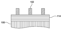
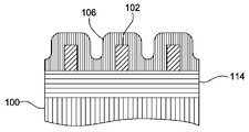
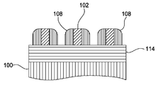
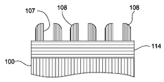
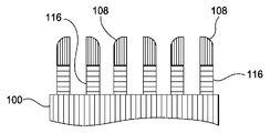
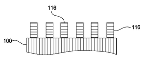
자기-정렬 이중 패터닝(Self-aligned double patterning, SADP)은 최소 피치를 넘어서 포토리소그래피 기술들의 능력들을 확장하기 위한 하나의 방법이다. 이러한 방법은 도 1a-1f에 도시되어 있다. 도 1a를 참조하면, 표준 포토리소그래피 및 식각 기술들을 이용하여, 패터닝된 코어 피쳐(core feature)들(102)이 기판(100) 상의 유전체 층(114) 위에 희생 구조 재료(sacrificial structural material)로부터 형성된다. 패터닝된 피쳐들은 종종 플레이스홀더(placeholder)들 또는 코어들로서 지칭되며, 그리고 고 분해능(high-resolution) 포토마스크를 이용하는 포토리소그래피 시스템의 광학 분해능(optical resolution)에 가까운 간격들 및/또는 선폭들을 갖는다. 이후, 도 1b에 나타낸 바와 같이, 실리콘 산화물과 같은 하드 마스크 재료의 등각적인(conformal) 층(106)이 코어 피쳐들(102) 위에 증착된다. 그런 다음, 도 1c에 나타낸 바와 같이, 이방성 플라즈마 식각을 이용하여 수평 표면들로부터 하드 마스크 재료를 우선적으로 식각함으로써 코어 피쳐들(102)의 측면(side)들 상에 하드 마스크 스페이서들(108)이 형성되어, 패터닝된 코어 피쳐들(102) 위에 증착된 하드 마스크 재료를 개방할 뿐 아니라, 2개의 측벽들 사이의 바닥에 증착된 하드 마스크 재료를 제거한다. 그런 다음, 패터닝된 코어 피쳐들(102)이 제거되어, 하드 마스크 스페이서들(108)을 남길 수 있다(도 1d). 이 시점(point)에서, 도 1e에 나타낸 바와 같이, 하드 마스크 스페이서들(108)은 유전체 리브(dielectric rib)들(116)을 형성하기 위해 유전체 층(114)에 패턴을 전사하기 위한 식각 마스크로서 이용될 수 있다. 이후, 하드 마스크 스페이서들(108)이 제거된다(도 1f). 따라서, 유전체 리브들(116)의 밀도는 포토리소그래피적으로(photolithographically) 패터닝된 코어 피쳐들(102)의 밀도의 두배이며, 그리고 유전체 리브들(116)의 피치는 패터닝된 코어 피쳐들(102)의 피치의 절반(half)이다. Self-aligned double patterning (SADP) is one way to extend the capabilities of photolithographic techniques beyond the minimum pitch. Such a method is shown in Figs. 1A-1F. Referring to FIG. 1A, patterned
현재, 하드 마스크 스페이서들(108)은, 이를 테면 실리콘 산화물들과 같은 식각가능한(etchable) 재료를 이용하여 원자 층 증착(ALD)에 의해 형성된다. 전형적으로, 이러한 산화물들은 매우 낮은 온도(예를 들어, 200℃ 미만)에서 증착된다. 결과적으로, 재료 품질이 빈약하며(poor), 낮은 밀도, 빈약한 기계적 강도, 및 이후의 식각 케미스트리(etching chemistry)들에 대한 저하된 내화학성(chemical resistance)을 갖는다. 하드 마스크 재료를 식각하는 동안, 스페이서 측벽들, 예를 들어 측벽들(107)(도 1d)이 플라즈마에 노출된다. 전형적인 ALD 하드 마스크 스페이서들의 빈약한 재료 품질로 인해, 측벽들이 손상되며, 그에 따라 더 높은 라인 에지 거칠기(line edge roughness)를 유발한다. 이러한 문제는 축소되는 피쳐 크기에 대해 심각해진다. At present,
따라서, 패터닝 무결성(patterning integrity)이 크게 개선되도록 하드 마스크 스페이서들의 측벽들을 보호하는 방법이 필요하다. Accordingly, a need exists for a method of protecting the sidewalls of hard mask spacers to significantly improve patterning integrity.
본 발명의 실시예들은 식각 프로세스 동안 하드 마스크 스페이서들의 측벽들을 보호하기 위한 방법을 제공한다. 일 실시예에서, 프로세싱 챔버 내에서 기판 상에 질소-도핑된 비정질 탄소 층(nitrogen-doped amorphous carbon layer)을 형성하는 방법이 제공된다. 방법은 일반적으로, 기판 위에 미리결정된 두께의 희생 유전체 층을 증착하는 단계; 기판의 상부 표면(upper surface)을 노출시키기 위해 희생 유전체 층의 부분들을 제거함으로써, 기판 상에 패터닝된 피쳐들을 형성하는 단계; 기판의 노출된 상부 표면 및 패터닝된 피쳐들 상에 미리 결정된 두께의 질소-도핑된 비정질 탄소 층을 등각적으로(conformally) 증착하는 단계; 질소-도핑된 비정질 탄소 층으로부터 형성되는 측벽 스페이서들 내에 채워지는 패터닝된 피쳐들을 제공하기 위해, 이방성 식각 프로세스를 이용하여 기판의 상부 표면 및 패터닝된 피쳐들의 상부 표면으로부터 질소-도핑된 비정질 탄소 층을 선택적으로 제거하는 단계; 및 기판으로부터 패터닝된 피쳐들을 제거하는 단계를 포함한다. Embodiments of the present invention provide a method for protecting the sidewalls of hard mask spacers during an etch process. In one embodiment, a method of forming a nitrogen-doped amorphous carbon layer on a substrate in a processing chamber is provided. The method generally includes depositing a sacrificial dielectric layer of predetermined thickness over a substrate; Forming patterned features on the substrate by removing portions of the sacrificial dielectric layer to expose an upper surface of the substrate; Depositing conformally a nitrogen-doped amorphous carbon layer of a predetermined thickness on the exposed upper surface of the substrate and the patterned features; Doped amorphous carbon layer from the top surface of the substrate and the top surface of the patterned features using an anisotropic etch process to provide patterned features that are filled in the sidewall spacers formed from the nitrogen-doped amorphous carbon layer Selectively removing; And removing the patterned features from the substrate.
다른 실시예에서, 프로세싱 챔버 내에서 디바이스를 형성하는 방법이 제공된다. 방법은 일반적으로, 기판의 상부 표면 상에 패터닝된 피쳐들을 형성하는 단계; 기판의 노출된 상부 표면 및 패터닝된 피쳐들 상에 미리결정된 두께의 희생 유전체 층을 등각적으로 증착하는 단계; 희생 유전체 층으로부터 형성되는 제 1 측벽 스페이서들을 내에 채워지는 패터닝된 피쳐들을 제공하기 위해, 기판의 노출된 상부 표면 및 패터닝된 피쳐들의 상부 표면으로부터 희생 유전체 층을 선택적으로 제거하는 단계; 제 1 측벽 스페이서들에 인접하는 제 2 측벽 스페이서들을 형성하는 단계 ― 제 2 측벽 스페이서들은 약 0.1% 질소 내지 약 4.0% 질소의 탄소:질소 비율을 갖는 질소-도핑된 비정질 탄소 재료로부터 형성됨 ―; 및 제 1 측벽 스페이서들 내에 채워진 패터닝된 피쳐들을 제거하는 단계를 포함한다. In another embodiment, a method of forming a device in a processing chamber is provided. The method generally includes forming patterned features on an upper surface of a substrate; Isotropically depositing a sacrificial dielectric layer of a predetermined thickness on the exposed upper surface and patterned features of the substrate; Selectively removing the sacrificial dielectric layer from the exposed upper surface of the substrate and the upper surface of the patterned features to provide patterned features that are filled within the first sidewall spacers formed from the sacrificial dielectric layer; Forming second sidewall spacers adjacent to the first sidewall spacers, wherein the second sidewall spacers are formed from a nitrogen-doped amorphous carbon material having a carbon: nitrogen ratio of from about 0.1% nitrogen to about 4.0% nitrogen; And removing patterned features filled in the first sidewall spacers.
또 다른 실시예에서, 프로세싱 챔버 내에서 기판 상에 질소-도핑된 비정질 탄소 층을 형성하는 방법이 제공된다. 방법은 일반적으로, 기판 상에 형성된 패터닝된 피쳐들 상에 질소-도핑된 비정질 탄소 층을 등각적으로 증착하는 단계 ― 증착은 질소-함유 탄화수소 소스 및 플라즈마-개시 가스(plasma-initiating gas)를 프로세싱 챔버 내로 유입시킴으로써 수행되고, 질소-함유 탄화수소 소스는 벤조니트릴(benzonitrile)을 포함함 ―; 질소-도핑된 비정질 탄소 층으로부터 형성되는 측벽 스페이서들 내에 채워지는 패터닝된 피쳐들을 제공하기 위해, 이방성 식각 프로세스를 이용하여 기판의 상부 표면 및 패터닝된 피쳐들의 상부 표면으로부터 질소-도핑된 비정질 탄소 층을 선택적으로 제거하는 단계; 및 기판으로부터 패터닝된 피쳐들을 제거하는 단계를 포함한다. In yet another embodiment, a method of forming a nitrogen-doped amorphous carbon layer on a substrate in a processing chamber is provided. The method generally includes conformally depositing a nitrogen-doped amorphous carbon layer on patterned features formed on a substrate, the deposition comprising processing a nitrogen-containing hydrocarbon source and a plasma-initiating gas Wherein the nitrogen-containing hydrocarbon source comprises benzonitrile; Doped amorphous carbon layer from the top surface of the substrate and the top surface of the patterned features using an anisotropic etch process to provide patterned features that are filled in the sidewall spacers formed from the nitrogen-doped amorphous carbon layer Selectively removing; And removing the patterned features from the substrate.
본 발명의 상기 열거된 특징들이 상세히 이해될 수 있는 방식으로 앞서 간략히 요약된 본 발명의 보다 구체적인 설명이 실시예들을 참조로 하여 이루어질 수 있는데, 이러한 실시예들 중 일부는 첨부된 도면들에 예시되어 있다. 그러나, 첨부된 도면들은 본 발명의 단지 전형적인 실시예들을 도시하는 것이므로 본 발명의 범위를 제한하는 것으로 간주되지 않아야 한다는 것이 주목되어야 하는데, 이는 본 발명이 다른 균등하게 유효한 실시예들을 허용할 수 있기 때문이다.
도 1a-1f는 통상의 이중 패터닝 프로세스를 나타내는 단면도들을 도시한다.
도 2는 본 발명의 일 실시예에 따른 예시적인 패터닝 프로세스와 관련된 단계들을 도시하는 흐름도(flowchart)이다.
도 3a-3e는 도 2에서 설명된 단계들에 의해 형성되는 구조의 단면도들을 도시한다.
도 4는 본 발명의 다른 실시예에 따른 예시적인 패터닝 프로세스와 관련된 단계들을 도시하는 흐름도이다.
도 5a-5h는 도 4에서 설명된 단계들에 의해 형성되는 구조의 단면도들을 도시한다. A more particular description of the invention, briefly summarized above, in such a manner that the recited features of the invention may be understood in detail, may be made by reference to embodiments, some of which are illustrated in the accompanying drawings have. It should be noted, however, that the appended drawings illustrate only typical embodiments of this invention and are therefore not to be considered limiting of its scope, for the invention may admit to other equally effective embodiments to be.
1A-1F show cross-sectional views illustrating a conventional dual patterning process.
Figure 2 is a flowchart illustrating the steps associated with an exemplary patterning process in accordance with one embodiment of the present invention.
Figures 3A-3E show cross-sectional views of structures formed by the steps described in Figure 2;
4 is a flow chart illustrating steps associated with an exemplary patterning process in accordance with another embodiment of the present invention.
Figures 5A-5H show cross-sectional views of structures formed by the steps described in Figure 4;
본 발명의 실시예들은 초-등각적인(ultra-conformal) 스트립가능한(strippable) 스페이서 프로세스에 관한 것이다. 다양한 실시예들에서, 고 분해능 포토마스크를 이용하여 패터닝된 희생 구조 재료의 피쳐들 위에, 비정질 탄소와 같은 초-등각적인 탄소-기반 재료가 증착된다. 초-등각적인 탄소-기반 재료는 애싱(ashing) 또는 식각 프로세스 동안 보호 층으로서 기능함으로써, 탄소-기반 스페이서들에 의해 보호되는 측벽들 및 노출된 상부 표면을 갖는 희생 구조 재료를 남긴다. 희생 구조 재료를 제거하게 되면, 남아있는 탄소-기반 스페이서들은 아래에 있는(underlying) 층 또는 구조를 식각하기 위한 하드마스크 층의 역할을 수행할 수 있다. 일 예에서, 탄소-기반 재료는 도핑되지 않은 또는 탄소-도핑된 비정질 탄소 재료일 수 있다. Embodiments of the present invention are directed to an ultra-conformal strippable spacer process. In various embodiments, a super-conformal carbon-based material such as amorphous carbon is deposited over features of the patterned sacrificial material using a high resolution photomask. The super-conformal carbon-based material functions as a protective layer during an ashing or etching process, leaving a sacrificial material having sidewalls and exposed top surfaces that are protected by carbon-based spacers. Upon removal of the sacrificial material, the remaining carbon-based spacers may serve as a hard mask layer for etching the underlying layer or structure. In one example, the carbon-based material may be undoped or carbon-doped amorphous carbon material.
본 발명의 실시예들은 플라즈마 강화 화학 기상 증착(PECVD) 챔버와 같은 임의의 적합한 프로세싱 챔버를 이용하여 수행될 수 있다. 프로세싱 챔버는 기판 프로세싱 시스템 내에 포함될 수 있다. 본 발명을 실행하는 데에 이용될 수 있는 예시적인 기판 프로세싱 시스템은, 2002년 4월 2일 Salvador 등에게 특허가 허여되었으며 인용에 의해 본원에 포함되는, 본원과 양수인이 동일한 미국 특허 번호 6,364,954호에서 설명된다. 적합한 시스템들의 예들은 DxZTM 프로세싱 챔버를 이용할 수 있는 CENTURA![]()
![]()
![]()
![]()
a-C a-C 보호 층을The protective layer 이용하는 예시적인 제조 Exemplary Manufacture Using 시퀀스sequence
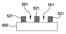
도 2는 본 발명의 일 실시예에 따른 예시적인 자기 정렬(self-aligned) 이중 패터닝 프로세스와 관련된 단계들을 도시하는 프로세스 흐름도이다. 도 3a-3e는 도 2에서 설명된 단계들에 의해 형성되는 구조의 단면도들을 도시한다. 자기 정렬 이중 패터닝 프로세스는 예시의 목적으로 선택된 것임이 고려된다. 본 발명의 개념은, 단일 또는 이중 패터닝 방식(scheme)의 다른 프로세스들, 이를 테면, NAND 플래시 적용예, DRAM 적용예, 또는 CMOS 적용예 등과 같은 다양한 반도체 프로세스들에서 요구되는 바와 같은 보호 희생 층 또는 가변(variable) 선폭 및 간격을 갖는 보호 스페이서들의 이용을 필요로 할 수 있는, 이를 테면, 비아/홀 수축 프로세스(via/hole shrink process), SATP(self-aligned triple patterning) 프로세스, 또는 SAQP(self-aligned quadruple patterning) 프로세스 등에 동등하게 적용가능하다. 또한, 도 2에 도시된 단계들의 개수 및 시퀀스들은 본원에서 설명되는 본 발명의 범위를 제한하는 것으로 의도되지 않는데, 왜냐하면 본원에서 설명되는 본 발명의 기본 범위를 벗어나지 않으면서, 하나 또는 그 초과의 단계들이 부가되고, 삭제되고, 및/또는 재배열될(reordered) 수 있기 때문이다. 2 is a process flow diagram illustrating steps associated with an exemplary self-aligned dual patterning process in accordance with one embodiment of the present invention. Figures 3A-3E show cross-sectional views of structures formed by the steps described in Figure 2; It is contemplated that the self-aligned dual patterning process is selected for illustrative purposes. The concepts of the present invention may be applied to other processes of a single or dual patterning scheme, such as a protective sacrificial layer as required in various semiconductor processes, such as NAND flash applications, DRAM applications, or CMOS applications, A via / hole shrink process, a self-aligned triple patterning (SATP) process, or a self-aligned triple patterning (SAQP) process, which may require the use of protective spacers with variable line widths and spacing -aligned quadruple patterning) process. Also, the number and sequence of steps shown in FIG. 2 are not intended to limit the scope of the invention described herein, Deleted, and / or rearranged, depending on the application.
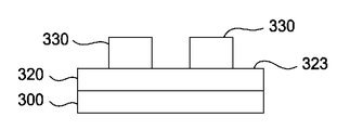
프로세스(200)는, 박스(202)에서, 기판(300) 상에 희생 구조 층(320)을 형성함으로써 시작된다. 희생 구조 층(320)은, 이를 테면 실리콘 산화물, 실리콘 질화물, 또는 폴리실리콘과 같은 실리콘-기반 재료일 수 있다. 대안적으로, 희생 구조 층(320)은, 이를 테면 비정질 탄소들과 같은 탄소-기반 재료일 수 있다. 탄소-기반 희생 구조 층이 요구되는 경우들에서, 희생 구조 층(320)은 비정질 탄소와 수소의 조합(수소화된(hydrogenated) 비정질 탄소 필름)일 수 있다. 하나의 예시적인 비정질 탄소 필름은 스트립가능한 APF(Advanced Patterning FilmTM) 재료일 수 있으며, 이는 캘리포니아 산타클라라에 소재하는 Applied Materials, Inc.로부터 상업적으로 입수가능하다. 희생 구조 층(320)에 대해 이용되는 재료들의 선택은, 희생 구조 층(320) 위에 형성될 등각적인 보호 층에 대한 식각/애싱 레이트에 따라 달라질 수 있음이 고려된다. 나타내지는 않았지만, 탄소-기반 희생 구조 층이 이용되는 특정 실시예들에서, 리소그래피 패터닝 프로세스 동안 광의 반사를 제어하기 위해, 탄소-기반 희생 구조 층 상에 하나 또는 그 초과의 반사 방지(anti-reflective) 코팅 층들이 증착될 수 있다. 적합한 반사 방지 코팅 층은 실리콘 이산화물, 실리콘 산질화물, 실리콘 질화물, 또는 이들의 조합들을 포함할 수 있다. 하나의 예시적인 반사 방지 코팅 층은, 캘리포니아 산타클라라에 소재하는 Applied Materials, Inc.로부터 상업적으로 입수가능한 DARCTM 재료일 수 있다. The
기판(300)은 나타낸 바와 같이 실질적으로 평평한 표면(323)을 가질 수 있다. 대안적으로, 기판(300)은, 표면 내에 트렌치들, 홀들, 또는 비아들이 형성되어 있는 패터닝된 구조들을 가질 수 있다. 기판(300)이 단일 바디(single body)로서 도시되어 있지만, 기판(300)은, 이를 테면 금속 컨택들, 트렌치 격리부(trench isolation)들, 게이트들, 비트라인들 또는 임의의 다른 배선(interconnect) 피쳐들과 같은, 반도체 디바이스들을 형성하는 데에 이용되는 하나 또는 그 초과의 재료들을 포함할 수 있다. 일 실시예에서, 기판(300)은, 반도체 디바이스들을 제조하는 데에 이용되는, 하나 또는 그 초과의 금속 층들, 하나 또는 그 초과의 유전체 재료들, 반도체 재료 및 이들의 조합들을 포함할 수 있다. 예를 들어, 기판(300)은, 적용예에 따라, 산화물 재료, 질화물 재료, 폴리실리콘 재료 등을 포함할 수 있다. 메모리 적용예가 요구되는 경우들에서, 기판(300)은 실리콘 기판 재료, 산화물 재료, 및 질화물 재료를 포함할 수 있으며, 중간에 샌드위칭되는(sandwiched) 폴리실리콘을 갖거나 또는 갖지 않는다.
몇몇 실시예들에서, 기판(300)은, 기판의 표면(미도시) 상에 증착되는, 복수의 교번하는(alternatng) 산화물 및 질화물 재료들(즉, 산화물-질화물-산화물(ONO)), 하나 또는 그 초과의 산화물 또는 질화물 재료들, 폴리실리콘 또는 비정질 실리콘 재료들, 비정질 실리콘과 교번하는 산화물들, 폴리실리콘과 교번하는 산화물들, 도핑된 실리콘과 교번하는 도핑되지 않는 실리콘, 도핑된 폴리실리콘과 교번하는 도핑되지 않은 폴리실리콘, 또는 도핑된 비정질 실리콘과 교번하는 도핑되지 않은 비정질 실리콘을 포함할 수 있다. 기판(300)은 다음의 것들: 결정질 실리콘, 실리콘 산화물, 실리콘 산질화물, 실리콘 질화물, 스트레인드(strained) 실리콘, 실리콘 게르마늄, 텅스텐, 티타늄 질화물, 도핑된 또는 도핑되지 않은 폴리실리콘, 도핑된 또는 도핑되지 않은 실리콘 웨이퍼들 및 패터닝된 또는 패터닝되지 않은 웨이퍼들, 실리콘 온 인슐레이터(SOI), 탄소 도핑된 실리콘 산화물들, 실리콘 질화물들, 도핑된 실리콘, 게르마늄, 갈륨 비소, 유리, 사파이어, 로우(low) k 유전체들, 및 이들의 조합들 중에서 하나 또는 그 초과를 포함하는 재료 또는 층 스택일 수 있다. In some embodiments, the
박스(204)에서, 도 3a에 나타낸 바와 같이, 이를 테면 포토레지스트 재료와 같은 레지스트 층(330)이 희생 구조 층(320) 상에 증착된다. In
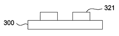
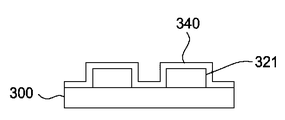
박스(206)에서, 도 3b에 나타낸 바와 같이, 표준 포토리소그래피 및 식각 기술들을 이용하여, 희생 구조 층(320)으로부터 형성되는 패터닝된 피쳐들(321)이 기판(300) 상에 생성된다. 패터닝된 피쳐들은 임의의 적합한 재료, 예를 들어 산화물들(이를 테면, 실리콘 이산화물, 실리콘 산질화물), 또는 질화물들(이를 테면, 실리콘 질화물)로 형성될 수 있다. 패터닝된 피쳐들은 플레이스홀더들, 맨드릴(mandrel)들 또는 코어들로서 종종 지칭되며, 그리고 이용되는 포토레지스트 재료에 기초하여 특정의 선폭들 및/또는 간격들을 갖는다. 패터닝된 피쳐들(321)의 폭은, 레지스트 층(330)으로 하여금 트리밍 프로세스(trimming process)를 받게 함으로써 조정될 수 있다. 희생 구조 층(320) 내로 패턴이 전사된 후, 적합한 포토레지스트 스트리핑 프로세스를 이용하여, 임의의 잔여 포토레지스트 및 하드 마스크 재료(이용되는 경우)가 제거된다. At
박스(208)에서, 도 3c에 나타낸 바와 같이, 기판(300)의 노출된 표면들 및 패터닝된 피쳐들(321) 상에 탄소-기반 보호 층(340)이 등각적으로 또는 실질적으로 등각적으로 증착된다. 탄소-기반 보호 층(340)의 두께는 약 5Å 내지 약 200Å일 수 있다. 일 실시예에서, 탄소-기반 보호 층은 비정질 탄소(a-C) 층이다. 비정질 탄소는 도핑되지 않거나, 또는 질소로 도핑될 수 있다. 일 예에서, 탄소-기반 보호 층(340)은 질소-도핑된 비정질 탄소 층이다. 질소-도핑된 비정질 탄소 층은, 이를 테면 플라즈마 강화 화학 기상 증착(PECVD) 프로세스와 같은 임의의 적합한 증착 기술들에 의해 증착될 수 있다. 일 실시예에서, 질소-도핑된 비정질 탄소 층은, 특히, 탄화수소 소스, N2 또는 NH3와 같은 질소-함유 가스, 및 플라즈마-개시 가스를 PECVD 챔버 내로 유동시킴으로써 증착될 수 있다. 다른 실시예에서, 질소-도핑된 비정질 탄소 층은, 특히, 캐리어 가스 내에 혼입된(entrained) 액상(liquid-phase) 탄화수소 또는 기상(gas-phase) 탄화수소와 같은 탄화수소 소스, 질소-함유 탄화수소 소스, 및 플라즈마-개시 가스를 PECVD 챔버 내로 유동시킴으로써 증착될 수 있다. 탄화수소 소스는 하나 또는 그 초과의 탄화수소 화합물들의 혼합물일 수 있다. 몇몇 실시예들에서는, 탄화수소 소스가 요구되지 않을 수도 있다. 대신에, 질소-함유 탄화수소 소스 및 플라즈마-개시 가스가 PECVD 챔버 내로 유동되어, 기판(300)의 노출된 표면들 및 패터닝된 피쳐들(321) 상에 질소-도핑된 비정질 탄소 보호 층을 형성한다. At
탄화수소 화합물들은, 탄화수소 화합물들의 불소-, 산소-, 히드록실기(hydroxyl group)-, 및 붕소-함유 유도체들을 포함하는, 탄화수소 화합물들의 부분적으로 또는 완전히 도핑된 유도체들일 수 있다. 탄화수소 소스 내에 포함될 수 있는 탄화수소 화합물들 또는 그 유도체들은 화학식 CxHy에 의해 설명될 수 있으며, 여기서 x는 1 내지 10의 범위를 가지며 그리고 y는 2 내지 30의 범위를 갖는다. 적합한 탄화수소 화합물들은, 제한되는 것은 아니지만, 아세틸렌(C2H2), 에탄(C2H6), 프로필렌(C3H6), 프로핀(C3H4), 프로판(C3H8), 부탄(C4H10), 부틸렌(C4H8), 부틴(C4H6), 비닐아세틸렌, 페닐아세틸렌(C8H6), 벤젠, 스티렌, 톨루엔, 크실렌, 에틸벤젠, 아세토페톤, 메틸 벤조에이트, 페닐 아세테이트, 페놀, 크레졸, 푸란, 알파-테르피넨, 시멘, 1,1,3,3,-테트라메틸부틸벤젠, t-부틸에테르, t-부틸에틸렌, 메틸-메타아크릴레이트, 및 화학식 C3H2 및 C5H4를 갖는 화합물들인, t-부틸푸르푸릴에테르(butylfurfurylether), 모노플루오로벤젠, 디플루오로벤젠들, 테트라플루오로벤젠들, 헥사플루오로벤젠들 등을 포함할 수 있다. 부가적인 적합한 탄화수소들은 에틸렌, 펜텐, 부타디엔, 이소프렌, 펜타디엔, 헥사디엔, 모노플루오로에틸렌, 디플루오로에틸렌들, 트리플루오로에틸렌, 테트라플루오로에틸렌, 모노클로로에틸렌, 디클로로에틸렌, 트리클로로에틸렌, 테트라클로로에틸렌 등을 포함할 수 있다. The hydrocarbon compounds may be partially or fully doped derivatives of hydrocarbon compounds, including fluorine-, oxygen-, hydroxyl group-, and boron-containing derivatives of the hydrocarbon compounds. The hydrocarbon compounds or derivatives thereof that may be included in the hydrocarbon source may be described by the formula CxHy where x ranges from 1 to 10 and y ranges from 2 to 30. [ Suitable hydrocarbon compounds include, but are not limited to, acetylene (C 2 H 2 ), ethane (C 2 H 6 ), propylene (C 3 H 6 ), propyne (C 3 H 4 ), propane (C 3 H 8 ) , butane (C 4 H 10), butylene (C 4 H 8), butyne (C 4 H 6), vinyl acetylene and phenyl acetylene (C 8 H 6), benzene, styrene, toluene, xylene, ethylbenzene, acetonitrile T-butyl ether, t-butyl ethylene, methyl-methacrylic acid, methyl methacrylate, methyl methacrylate, And compounds having the formulas C 3 H 2 and C 5 H 4 , such as t-butylfurfurylether, monofluorobenzene, difluorobenzenes, tetrafluorobenzenes, hexafluorobenzenes, And the like. Additional suitable hydrocarbons include ethylene, pentene, butadiene, isoprene, pentadiene, hexadiene, monofluoroethylene, difluoroethylene, trifluoroethylene, tetrafluoroethylene, monochloroethylene, dichloroethylene, trichlorethylene , Tetrachlorethylene, and the like.
질소 함유 탄화수소 소스 내에 포함될 수 있는 질소 함유 탄화수소 화합물들 또는 그 유도체들은 화학식 CxHyNz에 의해 설명될 수 있으며, 여기서 x는 1 내지 12의 범위를 갖고, y는 2 내지 20의 범위를 가지며, 그리고 z는 1 내지 10의 범위를 갖는다. 적합한 질소 함유 탄화수소 화합물들은 다음의 화합물들: 메틸아민, 트리메틸아민, 트리메틸아민(TMA), 트리에틸아민, 아닐린, 퀴놀린, 피리딘, 아크릴로니트릴, 및 벤조니트릴 중에서 하나 또는 그 초과를 포함할 수 있다. Nitrogen containing hydrocarbon compounds or derivatives thereof that may be contained in a nitrogen containing hydrocarbon source can be illustrated by the formula CxHyNz wherein x ranges from 1 to 12, y ranges from 2 to 20, and z is 1 to 10. Suitable nitrogen containing hydrocarbon compounds may include one or more of the following compounds: methylamine, trimethylamine, trimethylamine (TMA), triethylamine, aniline, quinoline, pyridine, acrylonitrile, and benzonitrile .
특정 실시예들에서, 질소 도핑된 비정질 탄소 증착 프로세스는 탄화수소 화합물 이전에 및/또는 탄화수소 화합물과 동시에 PECVD 챔버 내에 유입되는 플라즈마-개시 가스의 이용을 포함할 수 있으며, 그리고 플라즈마가 개시되어 증착을 시작한다. 플라즈마-개시 가스는, 제한되는 것은 아니지만, 헬륨 가스, 수소 가스, 질소 가스, 아르곤 가스 및 이들의 조합들을 포함하는 고 이온화 전위 가스(high ionization potential gas)일 수 있다. 플라즈마-개시 가스는 또한, 헬륨 가스, 질소 가스 또는 아르곤 가스와 같은, 화학적으로 비활성인 가스일 수 있다. 가스들에 대한 적절한 이온화 전위들은 약 5eV(전자 전위) 내지 25 eV 이다. 플라즈마-개시 가스는 질소 함유 탄화수소 소스 및/또는 탄화수소 소스 이전에 PECVD 챔버 내로 유입될 수 있으며, 이에 의해 안정적인 플라즈마가 형성될 수 있게 하며 그리고 아킹(arcing)의 가능성들을 줄인다. 희석 가스(diluent gas) 또는 캐리어 가스로서 이용되는 비활성 가스, 이를 테면 아르곤이, 플라즈마-개시 가스, 질소 함유 탄화수소 소스, 탄화수소 소스, 또는 이들의 조합들과 함께 유입될 수 있다. 요구되는 경우, 특히 헬륨(He), 수소(H2), 질소(N2), 암모니아(NH3) 또는 이들의 조합들과 같은 적절한 희석 가스들이 가스 혼합물에 부가될 수 있다. Ar, He 및 N2는 비정질 탄소 층의 밀도 및 증착 레이트를 제어하기 위해 이용된다. 몇몇 경우들에서, H2 및/또는 NH3의 부가는 비정질 탄소 층의 수소 비율을 제어하기 위해 이용될 수 있다. 대안적으로, 증착 동안 희석 가스들이 이용되지 않을 수도 있다. In certain embodiments, the nitrogen doped amorphous carbon deposition process may include the use of a plasma-initiated gas that enters the PECVD chamber prior to and / or concurrently with the hydrocarbon compound and / or the plasma is initiated to initiate deposition do. The plasma-initiated gas may be a high ionization potential gas, including, but not limited to, helium gas, hydrogen gas, nitrogen gas, argon gas, and combinations thereof. The plasma-initiated gas may also be a chemically inert gas such as helium gas, nitrogen gas or argon gas. Suitable ionization potentials for gases are about 5 eV (electron potential) to 25 eV. The plasma-initiated gas may be introduced into the PECVD chamber prior to the nitrogen-containing hydrocarbon source and / or the hydrocarbon source, thereby allowing stable plasma to form and reducing the likelihood of arcing. An inert gas used as a diluent gas or a carrier gas, such as argon, a plasma-initiated gas, a nitrogen-containing hydrocarbon source, a hydrocarbon source, or combinations thereof, may be introduced. If desired, suitable dilution gases such as helium (He), hydrogen (H 2 ), nitrogen (N 2 ), ammonia (NH 3 ) or combinations thereof may be added to the gas mixture. Ar, He, and N 2 are used to control the density and deposition rate of the amorphous carbon layer. In some cases, the addition of H 2 and / or NH 3 may be used to control the hydrogen ratio of the amorphous carbon layer. Alternatively, diluent gases may not be used during deposition.
탄화수소 소스 및 질소-함유 가스를 이용하여, 질소-도핑된 비정질 탄소가 증착되는 경우들에 있어서, 질소-함유 가스는 약 1:100 내지 약 10: 1의 질소-함유 가스 대 탄화수소 소스 비율로 PECVD 챔버 내로 유입될 수 있다. In cases where nitrogen-doped amorphous carbon is deposited using a hydrocarbon source and a nitrogen-containing gas, the nitrogen-containing gas may be PECVD at a nitrogen-containing gas to hydrocarbon source ratio of about 1: 100 to about 10: May be introduced into the chamber.
다양한 실시예들에서, 질소 도핑된 비정질 탄소 층은, 약 0.5 Torr 또는 그 초과, 이를 테면 약 0.5 Torr 내지 약 20 Torr, 그리고 일 실시예에서는 약 2 Torr 또는 그 초과, 이를 테면 약 2 Torr 내지 약 12 Torr의 챔버 압력, 및 약 25℃ 내지 약 800℃의 기판 온도, 이를 테면 약 200℃ 내지 약 400℃의 온도에서 증착될 수 있다. 이러한 층을 증착할 때 샤워헤드와 기판 표면 간의 전극 간격은 200 mils 내지 5,000 mils 간격, 예를 들어 약 500 mills 간격일 수 있다. 특정 실시예들에서, 플라즈마가 이용되는 경우, 탄화수소 소스, 질소 도핑된 비정질 탄소 소스, 및 플라즈마-개시 가스가 PECVD 챔버 내로 유입되며, 플라즈마가 개시되어 증착을 시작한다. In various embodiments, the nitrogen-doped amorphous carbon layer has a thickness of about 0.5 Torr or greater, such as about 0.5 Torr to about 20 Torr, and in one embodiment about 2 Torr or greater, such as about 2 Torr to about A chamber pressure of 12 Torr, and a substrate temperature of from about 25 [deg.] C to about 800 [deg.] C, such as from about 200 [deg.] C to about 400 [deg.] C. When depositing such a layer, the electrode spacing between the showerhead and the substrate surface may be in the range of 200 mils to 5,000 mils, for example about 500 milliseconds. In certain embodiments, when a plasma is used, a hydrocarbon source, a nitrogen-doped amorphous carbon source, and a plasma-initiated gas are introduced into the PECVD chamber and a plasma is initiated to begin deposition.
약 0.01 W/cm2 내지 약 5 W/cm2, 이를 테면 약 0.8 W/cm2 내지 약 2.3 W/cm2, 예를 들어 2 W/cm2의, 기판 표면적(substrate surface area)에 대한 전력 밀도에서 RF 전력을 인가함으로써, 플라즈마가 발생될 수 있다. 300 mm 기판에 대해, 약 1 Watt 내지 약 2,000 watts, 이를 테면 약 10 W 내지 약 100 W의 전력이 인가될 수 있다. RF 전력은 단일 주파수 또는 이중 주파수일 수 있음이 주목된다. 단일 주파수 전력이 이용된다면, 주파수 전력은 약 10KHz 내지 약 30MHz 일 수 있다. 이중 주파수 RF 전력을 이용하여 플라즈마를 발생시킨다면, 혼합형(mixed) RF 전력이 이용될 수 있다. 혼합형 RF 전력은, 약 10 MHz 내지 약 30 MHz 범위, 예를 들어 약 13.56 MHz의 고 주파수 전력 뿐 아니라, 약 10 KHz 내지 약 1 MHz 범위, 예를 들어 약 350 KHz의 저 주파수 전력을 제공할 수 있다. 이중 주파수 RF 전력의 인가는 플럭스 및 이온 에너지의 독립적인 제어를 제공하는 것으로 믿어지는데, 왜냐하면 필름 표면에 부딪히는(hitting) 이온들의 에너지가 필름 밀도에 영향을 미치기 때문이다. 인가되는 RF 전력, 및 하나 또는 그 초과의 주파수들의 이용은, 이용되는 장비 및 기판 크기에 기초하여 달라질 수 있다. 특정 실시예들에서는, 단일 주파수 RF 전력의 인가가 이용될 수 있는데, 전형적으로는, 본원에서 설명되는 바와 같은 고 주파수 전력의 인가가 이용될 수 있다. About 0.01 W / cm 2 to about 5 W / cm 2, For instance from about 0.8 W / cm 2 to about 2.3 W / cm 2, for example 2 W / cm 2, electric power to the substrate surface (substrate surface area) By applying RF power at the density, a plasma can be generated. For a 300 mm substrate, a power of about 1 Watt to about 2,000 Watts, such as about 10 W to about 100 W, may be applied. It is noted that the RF power may be single frequency or dual frequency. If a single frequency power is used, the frequency power may be between about 10 KHz and about 30 MHz. If the plasma is generated using dual frequency RF power, mixed RF power can be used. The mixed RF power can provide a low frequency power in the range of about 10 MHz to about 30 MHz, for example about 13.56 MHz, as well as in the range of about 10 KHz to about 1 MHz, for example about 350 KHz have. The application of dual frequency RF power is believed to provide independent control of flux and ion energy because the energy of the hitting ions on the film surface affects film density. The applied RF power, and the use of one or more frequencies, may vary based on the equipment used and the substrate size. In certain embodiments, application of single frequency RF power may be used, typically, application of high frequency power as described herein may be used.
300 mm 원형 기판들을 프로세싱하기 위한 예시적인 증착 프로세스는, 특히, 플라즈마-개시 가스, 질소 함유 탄화수소 소스 및 희석 가스를 이용할 수 있다. 이러한 증착 프로세스는, 약 0 sccm 내지 약 50,000 sccm, 예를 들어 약 400 sccm 내지 약 8,000 sccm의 유량으로 헬륨 및/또는 아르곤과 같은 플라즈마-개시 가스를 공급하는 단계, 및 약 10 sccm 내지 약 2,000 sccm, 예를 들어 약 500 sccm 내지 약 1,500 sccm의 유량으로 질소 함유 탄화수소 소스를 공급하는 단계를 포함할 수 있다. 질소 함유 탄화수소 소스가 액체 전구체인 경우, 그러면 질소 함유 탄화수소 소스 유동은 15 mg/min 내지 2,000 mg/min, 예를 들어 100 mg/min 내지 1,000 mg/min 일 수 있다. NH3, He, Ar, H2, 또는 N2와 같은 희석 가스는 약 0 sccm 내지 약 5,000 sccm, 예를 들어 약 500 sccm 내지 약 1,000 sccm의 유량으로 공급될 수 있다. 증착 프로세스는, 약 5 W 내지 약 1,600 W, 예를 들어 약 10W 내지 약 100W의 이중 주파수 RF 전력, 약 0.5 Torr 내지 약 50 Torr, 예를 들어 약 5 torr 내지 약 15 Torr의 챔버 압력, 및 약 25℃ 내지 약 650℃, 예를 들어 약 200℃ 내지 약 400℃의 기판 온도를 이용하여 수행될 수 있다. 이러한 프로세스 범위는, 약 10Å/min 내지 약 30,000Å/min 범위의, 질소 도핑된 비정질 탄소 층에 대한 증착 레이트를 제공한다. 본원에서의 개시내용을 읽게 되면, 당업자라면 상이한 증착 레이트들의 질소 도핑된 비정질 탄소 필름을 생성하기 위해 적절한 프로세스 파라미터들을 계산할 수 있을 것이다. 증착된 상태(as-deposited)의 질소-도핑된 비정질 탄소 층은, 약 0.1% 질소 내지 약 4.0% 질소, 이를 테면 약 1.5% 내지 약 2% 범위의 조정가능한 탄소:질소 비율을 갖는다. 본원에서 설명되는 프로세스들에 의해 증착되는 질소 도핑된 비정질 탄소 재료들의 예는 다음과 같이 제공된다. Exemplary deposition processes for processing 300 mm circular substrates may utilize, in particular, plasma-initiated gases, nitrogen-containing hydrocarbon sources and diluent gases. Such a deposition process may include supplying a plasma-initiated gas such as helium and / or argon at a flow rate of from about 0 sccm to about 50,000 sccm, for example, from about 400 sccm to about 8,000 sccm, and a flow rate of from about 10 sccm to about 2,000 sccm , For example, a nitrogen containing hydrocarbon source at a flow rate between about 500 sccm and about 1,500 sccm. If the nitrogen containing hydrocarbon source is a liquid precursor then the nitrogen containing hydrocarbon source flow may be from 15 mg / min to 2,000 mg / min, for example from 100 mg / min to 1,000 mg / min. A diluent gas such as NH 3 , He, Ar, H 2 , or N 2 may be supplied at a flow rate of from about 0 sccm to about 5,000 sccm, such as from about 500 sccm to about 1,000 sccm. The deposition process may be performed using a dual frequency RF power of about 5 W to about 1,600 W, e.g., about 10 W to about 100 W, a chamber pressure of about 0.5 Torr to about 50 Torr, e.g., about 5 torr to about 15 Torr, For example, from about 25 [deg.] C to about 650 [deg.] C, for example, from about 200 [deg.] C to about 400 [deg.] C. This process range provides deposition rates for nitrogen doped amorphous carbon layers ranging from about 10 A / min to about 30,000 A / min. Having read the disclosure herein, those skilled in the art will be able to calculate appropriate process parameters to produce nitrogen-doped amorphous carbon films of different deposition rates. The as-deposited nitrogen-doped amorphous carbon layer has an adjustable carbon: nitrogen ratio ranging from about 0.1% nitrogen to about 4.0% nitrogen, such as from about 1.5% to about 2%. An example of nitrogen doped amorphous carbon materials deposited by the processes described herein is provided as follows.
질소 도핑된 비정질 탄소 증착 프로세스는, 약 10Å 내지 약 1,000Å의 두께를 갖는 질소 도핑된 비정질 탄소 층을 생성하기 위해, 프로세싱 챔버에 약 200 sccm 내지 1,500 sccm, 예를 들어 약 500 sccm의 유량으로 헬륨을 제공하는 단계, 프로세싱 챔버에 약 100 mg/min 내지 약 1,000 mg/min의 유량으로 벤조니트릴을 제공하는 단계, 프로세싱 챔버에 약 0 sccm 내지 약 2,000 sccm의 유량으로 암모니아를 제공하는 단계, (200mm 웨이퍼에 대해) 약 30W 내지 200W의 고 주파수 RF 전력(13.56 MHz)을 인가하는 단계, 약 200℃ 내지 약 550℃의 증착 온도를 유지하는 단계, 및 약 100 mils 내지 약 800 mils의 간격을 가지면서, 약 2 Torr 내지 15 Torr의 챔버 압력을 유지하는 단계를 포함할 수 있다. The nitrogen doped amorphous carbon deposition process may be performed in a processing chamber at a flow rate between about 200 sccm and about 1,500 sccm, such as about 500 sccm, to produce a nitrogen doped amorphous carbon layer having a thickness of about 10 A to about 1, Providing benzonitrile to the processing chamber at a flow rate between about 100 mg / min and about 1,000 mg / min; providing ammonia at a flow rate between about 0 sccm and about 2,000 sccm to the processing chamber; Applying a high frequency RF power (13.56 MHz) of from about 30 W to about 200 W to the wafer, maintaining a deposition temperature of from about 200 [deg.] C to about 550 [deg.] C, , Maintaining a chamber pressure of about 2 Torr to 15 Torr.
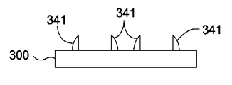
도 2를 다시 참조하면, 박스(210)에서, 도 3d에 나타낸 바와 같이, 패터닝된 피쳐들(321) 상에 탄소-기반 보호 층(340)이 등각적으로 증착된 후, 영역들(311) 내의 기판(300)의 상부 표면을 노출시키고 그리고 패터닝된 피쳐들(321)의 상부 표면을 노출시키기 위해, 탄소-기반 보호 층(340)이 이방성으로 식각(수직 식각)되어, 결과적으로, 탄소-기반 측벽 스페이서들(341)에 의해 보호되는 (희생 구조 층(320)으로부터 형성되는) 패터닝된 피쳐들(321)을 생성한다. Referring again to FIG. 2, at
박스(212)에서, 도 3e에 나타낸 바와 같이, (희생 구조 층(320)으로부터 형성되는) 패터닝된 피쳐들(321)이, 통상의 플라즈마 식각 프로세스 또는 다른 적합한 습식 스트리핑 프로세스를 이용하여 제거됨으로써, 비희생(non-sacrificial) 탄소-기반 측벽 스페이서들(341)을 남긴다. 플라즈마 식각 프로세스는, 기판 위의 플라즈마 내에 불소-기반 식각 케미스트리를 유입함으로써 행해질 수 있다. 개선된 재료 품질 및 커버리지(coverage)로 인해, 탄소-기반 측벽 스페이서들(341)은 손상되지 않는데, 왜냐하면 이러한 탄소-기반 측벽 스페이서들(341)은 불소-기반 반응성 식각 케미스트리 또는 습식 스트립-기반 케미스트리에 대해 매우 양호한 선택성(selectivity)을 갖기 때문이다. 패터닝된 피쳐들(321)을 제거하게 되면, 남아있는 탄소-기반 측벽 스페이서들(341)은, 아래에 있는 층, 층 스택, 또는 구조를 식각하기 위한 하드마스크로서 이용될 수 있다. 특히, 이러한 패터닝 프로세스에 따른 탄소-기반 측벽 스페이서들(341)의 밀도는 포토리소그래피적으로 패터닝된 피쳐들(321)의 밀도의 두배이며, 탄소-기반 측벽 스페이서들(341)의 피치는 패터닝된 피쳐들(321)의 피치의 절반이다. At
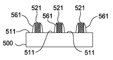
도 4는 본 발명의 다른 실시예에 따른 예시적인 패터닝 프로세스와 관련된 단계들을 도시하는 흐름도이다. 도 5a-5h는 도 4에서 설명된 단계들에 의해 형성되는 구조의 단면도들을 도시한다. 이러한 실시예의 개념은, 단일 또는 이중 패터닝 방식의 다른 프로세스들, 이를 테면, NAND 플래시 적용예, DRAM 적용예, 또는 CMOS 적용예 등과 같은 다양한 반도체 프로세스들에서 요구되는 바와 같은 보호 희생 층 또는 가변 선폭 및 간격을 갖는 보호 스페이서들의 이용을 필요로 할 수 있는, 이를 테면, 비아/홀 수축 프로세스, BEOL(back end of line) SADP(self-aligned double patterning) 프로세스, 또는 SAQP(self-aligned quadruple patterning) 프로세스 등에 동등하게 적용가능함이 주목된다. 4 is a flow chart illustrating steps associated with an exemplary patterning process in accordance with another embodiment of the present invention. Figures 5A-5H show cross-sectional views of structures formed by the steps described in Figure 4; The concept of this embodiment may be applied to a protective sacrificial layer or variable linewidth as required in various semiconductor processes, such as NAND flash applications, DRAM applications, or CMOS applications, and other processes in single or dual patterning schemes, A self-aligned quadruple patterning (SAQP) process, or a self-aligned quadruple patterning (SAQP) process, which may require the use of protective spacers having spacing, And the like.
프로세스(400)는, 박스(402)에서, 이를 테면 PECVD 챔버와 같은 프로세스 챔버 내에 기판(500)을 제공함으로써 시작된다. 도 3a에 나타낸 기판(300)과 관련하여 상기 논의된 바와 같이, 기판(500)은 실리콘 재료, 산화물 재료, 폴리실리콘 재료 등을 포함하는, 반도체 디바이스들을 형성하는 데에 이용되는 하나 또는 그 초과의 재료들일 수 있다. The
박스(404)에서, 도 5b에 나타낸 바와 같이, 비희생 구조 층(520)이 기판(500) 상에 증착된다. 비희생 구조 층(520)은 비정질 탄소들과 같은 탄소-기반 재료일 수 있다. 일 예에서, 비희생 구조 층(520)은, 캘리포니아 산타클라라에 소재하는 Applied Materials, Inc.로부터 상업적으로 입수가능한 APF(Advanced Patterning FilmTM) 재료이다. 나타내지는 않았지만, 탄소-기반 비희생 구조 층이 이용되는 특정 실시예들에서, 리소그래피 패터닝 프로세스 동안 광의 반사를 제어하기 위해, 탄소-기반 비희생 구조 층 상에 하나 또는 그 초과의 반사 방지 코팅 층들이 증착될 수 있다. 적합한 반사 방지 코팅 층은 실리콘 이산화물, 실리콘 산질화물, 실리콘 질화물, 또는 이들의 조합들을 포함할 수 있다. 하나의 예시적인 반사 방지 코팅 층은, 캘리포니아 산타클라라에 소재하는 Applied Materials, Inc.로부터 상업적으로 입수가능한 DARCTM 재료일 수 있다. In
박스(406)에서, 비희생 구조 층(520) 위에 바닥 반사 방지 코팅(bottom anti-reflective coating, BARC) 층(540)이 증착된다. BARC 층(540)은 폴리아미드들 및 폴리설폰들과 같은 유기 재료일 수 있다. BARC 층(540)은 이후의 레지스트 층의 패터닝 동안 광의 반사를 감소시키는 것으로 믿어지며, 그리고 더 얇은 레지스트 층들에 대해 또한 유익한데, 왜냐하면 BARC 층(540)은 아래에 있는 층 또는 구조를 식각하는 동안 개선된 식각 내성(etch resistance)을 위해 다중층 마스크(multi-layered mask)의 총 두께를 증가시키기 때문이다. 특정 실시예들에서, 도 5c에 나타낸 바와 같이, 포토리소그래피 성능을 개선하기 위해, BARC 층(540)은 BARC 층(540)과 비희생 구조 층(520) 사이에 증착되는 광 흡수 층(530)을 더 포함할 수 있다. 광 흡수 층(530)은, 이를 테면 질화물들과 같은 금속 층일 수 있다. 일 예에서, 광 흡수 층(530)은 티타늄 질화물이다. At
그런 다음, 박스(408)에서, 이를 테면 포토레지스트 재료와 같은 레지스트 층이 BARC 층(540) 상에 증착된다. 이후, 도 5d에 나타낸 바와 같이, 리소그래피 프로세스에 의해 레지스트 층이 패터닝되어, 요구되는 식각 패턴(551)을 갖는 패터닝된 레지스트 층(550)을 생성한다. 예시적인 목적을 위해, 식각 패턴(551)은 상이한 패턴 폭을 갖는 것으로 나타나있다. Then, in
박스(410)에서, 도 5e에 나타낸 바와 같이, 요구되는 식각 패턴(551)을 비희생 구조 층(520) 내로 전사시키기 위해, 통상의 포토리소그래피 및 식각 프로세스들을 이용하여, BARC 층(540), 광 흡수 층(530) 및 비희생 구조 층(520)을 각각 패터닝함으로써, 패터닝된 비희생 피쳐들(521)을 남긴다.At
박스(412)에서, 기판(500)의 노출된 표면들 및 패터닝된 비희생 피쳐들(521) 상에 제 1 등각적인 층이 등각적으로 또는 실질적으로 등각적으로 증착된다. 제 1 등각적인 층은 패터닝된 희생 피쳐들(521)과 상이한 식각 레이트를 갖는 스트립가능한 재료를 포함할 수 있다. 제 1 등각적인 층을 위한 적합한 재료들은, 예를 들어 산화물들(이를 테면, 실리콘 이산화물, 실리콘 산질화물), 또는 질화물(이를 테면, 실리콘 질화물)을 포함할 수 있다. 그런 다음, 도 5f에 나타낸 바와 같이, 영역들(511) 내의 기판(500)의 상부 표면을 노출시키고 그리고 패터닝된 비희생 피쳐들(521)의 상부 표면을 노출시키기 위해, 제 1 등각적인 층이 이방성으로 식각되어, 결과적으로, 제 1 등각적인 층으로부터 형성되는 스트립가능한 측벽 스페이서들(561)에 의해 보호되는 (비희생 구조 층(520)으로부터 형성되는) 패터닝된 비희생 피쳐들(521)을 생성한다. At
그런 다음, 박스(414)에서, 도 5g에 나타낸 바와 같이, 비희생 탄소-기반 측벽 스페이서들(571)이, 측벽 스페이서들(561)과 유사한 방식으로, 패터닝된 비희생 피쳐들(521)에 인접하게 형성된다. 비희생 탄소-기반 측벽 스페이서들(571)은, 박스들(208 및 210)과 관련하여 상기 설명된 바와 같은 프로세스들에 의해 형성되는, 도핑되지 않은 또는 질소로 도핑된 비정질 탄소(a-C)일 수 있다. 일 실시예에서, 비희생 탄소-기반 측벽 스페이서들(571)은 질소-도핑된 비정질 탄소이다. 5g, non-sacrificial carbon-based
박스(416)에서, 도 5h에 나타낸 바와 같이, 통상의 습식 스트리핑 프로세스 또는 다른 적합한 프로세스를 이용하여, 패터닝된 비희생 피쳐들(521)과 비희생 탄소-기반 측벽 스페이서들(571) 사이에 위치된 스트립가능한 측벽 스페이서들(561)을 제거함으로써, 패터닝된 비희생 피쳐들(521) 및 비희생 탄소-기반 측벽 스페이서들(571)을 남긴다. 남아있는 패터닝된 비희생 피쳐들(521) 및 비희생 탄소-기반 측벽 스페이서들(571)은 이후, 아래의 층, 층 스택, 또는 구조를 식각하기 위한 하드마스크로서 이용될 수 있다. 특히, 이러한 패터닝 프로세스에 따른 결과적인 하드마스크(즉, 패터닝된 비희생 피쳐들(521) 및 비희생 탄소-기반 측벽 스페이서들(571))의 밀도는 패터닝된 레지스트 층(550)의 밀도의 3배이며, 결과적인 하드마스크(즉, 패터닝된 비희생 피쳐들(521) 및 비희생 탄소-기반 측벽 스페이서들(571))의 피치는 패터닝된 레지스트 층(550)의 피치의 절반이다. At
본 발명에 따라 증착되는 탄소-기반 보호층들 또는 측벽 스페이서들은, 약 1.5%의 개선된 필름 균일성, 약 1.25-1.60 g/cc의 높은 필름 밀도, 및 50 MPa 미만의 필름 압축 응력(compressive film stress)과 함께, 95% 보다 높은 우수한 등각성(conformality)을 제공할 수 있는 것으로 관찰되었다. 애싱 또는 이방성 플라즈마 식각 프로세스 동안 하드 마스크 스페이서들의 측벽들이 손상되지 않기 때문에, 실리콘 산화물 재료들을 이용하여 통상의 ALD에 의해 성장된 스페이서들과 비교하여, 라인 에지 거칠기가 상당히 감소된다. 따라서, 결과적인 하드 마스크 스페이서들은, 마이크로로딩(microloading)을 거의 갖지 않으면서 또는 아예 갖지 않으면서, 우수한 식각 프로파일 및 식각 선택성을 제공할 수 있다. The carbon-based protective layers or sidewall spacers deposited in accordance with the present invention may have improved film uniformity of about 1.5%, a high film density of about 1.25-1.60 g / cc, and a compressive film of less than 50 MPa stress, it is observed that it can provide excellent conformality higher than 95%. Since the sidewalls of the hard mask spacers are not damaged during the ashing or anisotropic plasma etch process, the line edge roughness is significantly reduced as compared to spacers grown by conventional ALD using silicon oxide materials. Thus, the resulting hard mask spacers can provide excellent etch profile and etch selectivity, with little or no microloading.
상기 내용이 본 발명의 실시예들에 관한 것이지만, 본 발명의 다른 및 추가의 실시예들이 본 발명의 기본적인 범위를 벗어나지 않으면서 안출될 수 있으며, 본 발명의 범위는 하기의 청구항들에 의해 결정된다. While the foregoing is directed to embodiments of the present invention, other and further embodiments of the invention may be devised without departing from the basic scope thereof, and the scope thereof is determined by the claims that follow .
Claims (15)
기판 위에 미리결정된 두께의 희생 유전체 층(sacrificial dielectric layer)을 증착하는 단계;
상기 기판의 상부 표면(upper surface)을 노출시키기 위해 상기 희생 유전체 층의 부분들을 제거함으로써, 상기 기판 상에 패터닝된 피쳐들(patterned features)을 형성하는 단계;
상기 기판의 노출된 상부 표면 및 상기 패터닝된 피쳐들 상에 미리 결정된 두께의 비정질 탄소 층을 등각적으로(conformally) 증착하는 단계;
상기 비정질 탄소 층으로부터 형성되는 측벽 스페이서들 내에 채워지는 상기 패터닝된 피쳐들을 제공하기 위해, 이방성 식각 프로세스를 이용하여 상기 기판의 상부 표면 및 상기 패터닝된 피쳐들의 상부 표면으로부터 상기 비정질 탄소 층을 선택적으로 제거하는 단계; 및
상기 기판으로부터 상기 패터닝된 피쳐들을 제거하는 단계
를 포함하는,
프로세싱 챔버 내에서 기판 상에 비정질 탄소 층을 형성하는 방법. 1. A method of forming an amorphous carbon layer on a substrate in a processing chamber,
Depositing a sacrificial dielectric layer of predetermined thickness over the substrate;
Forming patterned features on the substrate by removing portions of the sacrificial dielectric layer to expose an upper surface of the substrate;
Conformally depositing an amorphous carbon layer of a predetermined thickness on the exposed upper surface of the substrate and the patterned features;
Selectively removing the amorphous carbon layer from the top surface of the substrate and the top surface of the patterned features using an anisotropic etch process to provide the patterned features to be filled in sidewall spacers formed from the amorphous carbon layer ; And
Removing the patterned features from the substrate
/ RTI >
A method for forming an amorphous carbon layer on a substrate in a processing chamber.
상기 비정질 탄소 층은, 탄화수소 소스, 질소-함유 가스 및 플라즈마 개시 가스(plasma initiating gas)를 상기 프로세싱 챔버 내로 유입시킴으로써 형성되는,
프로세싱 챔버 내에서 기판 상에 비정질 탄소 층을 형성하는 방법. The method according to claim 1,
Wherein the amorphous carbon layer is formed by introducing a hydrocarbon source, a nitrogen-containing gas, and a plasma initiating gas into the processing chamber.
A method for forming an amorphous carbon layer on a substrate in a processing chamber.
상기 탄화수소 소스는,
아세틸렌(C2H2), 에틸렌(C2H4), 에탄(C2H6), 프로필렌(C3H6), 프로핀(C3H4), 프로판(C3H8), 부탄(C4H10), 부틸렌(C4H8), 부타디엔(C4H6), 페닐아세틸렌(C8H6) 및 이들의 조합들로 이루어진 그룹으로부터 선택되는 하나 또는 그 초과의 탄화수소 화합물들을 포함하는,
프로세싱 챔버 내에서 기판 상에 비정질 탄소 층을 형성하는 방법. 3. The method of claim 2,
The hydrocarbon source may comprise,
Acetylene (C 2 H 2), ethylene (C 2 H 4), ethane (C 2 H 6), propylene (C 3 H 6), propyne (C 3 H 4), propane (C 3 H 8), butane One or more hydrocarbon compounds selected from the group consisting of C 4 H 10 , butylene (C 4 H 8 ), butadiene (C 4 H 6 ), phenylacetylene (C 8 H 6 ) Lt; / RTI >
A method for forming an amorphous carbon layer on a substrate in a processing chamber.
상기 비정질 탄소 층은 질소-함유 탄화수소 소스 및 플라즈마-개시 가스를 상기 프로세싱 챔버 내로 유입시킴으로써 형성되는,
프로세싱 챔버 내에서 기판 상에 비정질 탄소 층을 형성하는 방법. The method according to claim 1,
Wherein the amorphous carbon layer is formed by introducing a nitrogen-containing hydrocarbon source and a plasma-initiated gas into the processing chamber.
A method for forming an amorphous carbon layer on a substrate in a processing chamber.
상기 질소-함유 탄화수소는,
메틸아민, 디메틸아민, 트리메틸아민(TMA), 트리에틸아민, 아닐린, 퀴놀린, 피리딘, 아크릴로니트릴, 벤조니트릴(benzonitrile) 및 이들의 조합들로 이루어진 그룹으로부터 선택되는 하나 또는 그 초과의 질소 함유 탄화수소 화합물들을 포함하는,
프로세싱 챔버 내에서 기판 상에 비정질 탄소 층을 형성하는 방법. 5. The method of claim 4,
The nitrogen-
One or more nitrogen-containing hydrocarbons selected from the group consisting of methylamine, dimethylamine, trimethylamine (TMA), triethylamine, aniline, quinoline, pyridine, acrylonitrile, benzonitrile, ≪ / RTI >
A method for forming an amorphous carbon layer on a substrate in a processing chamber.
상기 질소 함유 탄화수소 화합물은 벤조니트릴인,
프로세싱 챔버 내에서 기판 상에 비정질 탄소 층을 형성하는 방법. 6. The method of claim 5,
Wherein the nitrogen containing hydrocarbon compound is benzonitrile,
A method for forming an amorphous carbon layer on a substrate in a processing chamber.
상기 비정질 탄소 층은, 약 0.1% 질소 내지 약 4.0% 질소의 탄소:질소 비율을 갖는 질소-도핑된 비정질 탄소인,
프로세싱 챔버 내에서 기판 상에 비정질 탄소 층을 형성하는 방법. The method according to claim 1,
Wherein the amorphous carbon layer is a nitrogen-doped amorphous carbon having a carbon: nitrogen ratio of about 0.1% nitrogen to about 4.0% nitrogen,
A method for forming an amorphous carbon layer on a substrate in a processing chamber.
상기 희생 유전체 층은 실리콘 산화물, 실리콘 질화물, 폴리실리콘, 또는 비정질 탄소를 포함하는,
프로세싱 챔버 내에서 기판 상에 비정질 탄소 층을 형성하는 방법. The method according to claim 1,
Wherein the sacrificial dielectric layer comprises silicon oxide, silicon nitride, polysilicon, or amorphous carbon.
A method for forming an amorphous carbon layer on a substrate in a processing chamber.
기판의 상부 표면 상에 패터닝된 피쳐들을 형성하는 단계;
상기 기판의 노출된 상부 표면 및 상기 패터닝된 피쳐들 상에 미리결정된 두께의 희생 유전체 층을 등각적으로 증착하는 단계;
상기 희생 유전체 층으로부터 형성되는 제 1 측벽 스페이서들을 내에 채워지는 상기 패터닝된 피쳐들을 제공하기 위해, 상기 기판의 노출된 상부 표면 및 상기 패터닝된 피쳐들의 상부 표면으로부터 상기 희생 유전체 층을 선택적으로 제거하는 단계;
상기 제 1 측벽 스페이서들에 인접하는 제 2 측벽 스페이서들을 형성하는 단계 ― 상기 제 2 측벽 스페이서들은 약 0.1% 질소 내지 약 4.0% 질소의 탄소:질소 비율을 갖는 질소-도핑된 비정질 탄소 재료로부터 형성됨 ―; 및
상기 제 1 측벽 스페이서들 내에 채워진 상기 패터닝된 피쳐들을 제거하는 단계
를 포함하는,
프로세싱 챔버 내에서 디바이스를 형성하는 방법. 1. A method of forming a device in a processing chamber,
Forming patterned features on an upper surface of the substrate;
Isotropically depositing a sacrificial dielectric layer of a predetermined thickness on the exposed upper surface of the substrate and the patterned features;
Selectively removing the sacrificial dielectric layer from the exposed upper surface of the substrate and the upper surface of the patterned features to provide the patterned features to be filled in first sidewall spacers formed from the sacrificial dielectric layer ;
Forming second sidewall spacers adjacent to the first sidewall spacers, wherein the second sidewall spacers are formed from a nitrogen-doped amorphous carbon material having a carbon: nitrogen ratio of about 0.1% nitrogen to about 4.0% nitrogen, ; And
Removing the patterned features filled in the first sidewall spacers
/ RTI >
A method for forming a device in a processing chamber.
상기 패터닝된 피쳐들은 비정질 탄소로부터 형성되는,
프로세싱 챔버 내에서 디바이스를 형성하는 방법. 10. The method of claim 9,
Wherein the patterned features are formed from amorphous carbon,
A method for forming a device in a processing chamber.
상기 질소-도핑된 비정질 탄소 재료는, 질소-함유 탄화수소 소스 및 플라즈마-개시 가스를 상기 프로세싱 챔버 내로 유입시킴으로써 형성되는,
프로세싱 챔버 내에서 디바이스를 형성하는 방법. 10. The method of claim 9,
Wherein the nitrogen-doped amorphous carbon material is formed by introducing a nitrogen-containing hydrocarbon source and a plasma-initiated gas into the processing chamber,
A method for forming a device in a processing chamber.
상기 질소-함유 탄화수소 소스는,
메틸아민, 디메틸아민, 트리메틸아민(TMA), 트리에틸아민, 아닐린, 퀴놀린, 피리딘, 아크릴로니트릴, 벤조니트릴 및 이들의 조합들로 이루어진 그룹으로부터 선택되는 하나 또는 그 초과의 질소 함유 탄화수소 화합물들을 포함하는,
프로세싱 챔버 내에서 디바이스를 형성하는 방법. 12. The method of claim 11,
Said nitrogen-containing hydrocarbon source may comprise,
Containing hydrocarbon compounds selected from the group consisting of methylamine, dimethylamine, trimethylamine (TMA), triethylamine, aniline, quinoline, pyridine, acrylonitrile, benzonitrile and combinations thereof doing,
A method for forming a device in a processing chamber.
상기 질소 함유 탄화수소 화합물은 벤조니트릴인,
프로세싱 챔버 내에서 디바이스를 형성하는 방법. 13. The method of claim 12,
Wherein the nitrogen containing hydrocarbon compound is benzonitrile,
A method for forming a device in a processing chamber.
상기 기판 상에 형성된 패터닝된 피쳐들 상에 질소-도핑된 비정질 탄소 층을 등각적으로 증착하는 단계 ― 상기 증착은 질소-함유 탄화수소 소스 및 플라즈마-개시 가스(plasma-initiating gas)를 상기 프로세싱 챔버 내로 유입시킴으로써 수행되고, 상기 질소-함유 탄화수소 소스는 벤조니트릴을 포함함 ―;
상기 질소-도핑된 비정질 탄소 층으로부터 형성되는 측벽 스페이서들 내에 채워지는 패터닝된 피쳐들을 제공하기 위해, 이방성 식각 프로세스를 이용하여 상기 기판의 상부 표면 및 상기 패터닝된 피쳐들의 상부 표면으로부터 상기 질소-도핑된 비정질 탄소 층을 선택적으로 제거하는 단계; 및
상기 기판으로부터 상기 패터닝된 피쳐들을 제거하는 단계
를 포함하는,
프로세싱 챔버 내에서 기판 상에 질소-도핑된 비정질 탄소 층을 형성하는 방법. 1. A method of forming a nitrogen-doped amorphous carbon layer on a substrate in a processing chamber,
The method comprising the steps of conformally depositing a nitrogen-doped amorphous carbon layer on patterned features formed on the substrate, the deposition comprising introducing a nitrogen-containing hydrocarbon source and a plasma-initiating gas into the processing chamber Wherein the nitrogen-containing hydrocarbon source comprises benzonitrile;
Doped amorphous carbon layer is deposited on the upper surface of the substrate and the upper surface of the patterned features using an anisotropic etch process to provide patterned features that are filled in sidewall spacers formed from the nitrogen- Selectively removing the amorphous carbon layer; And
Removing the patterned features from the substrate
/ RTI >
A method for forming a nitrogen-doped amorphous carbon layer on a substrate in a processing chamber.
상기 질소-도핑된 비정질 탄소 층은,
약 100 mg/min 내지 약 1,000 mg/min의 유량으로 질소-함유 탄화수소 소스를 상기 프로세싱 챔버 내에 유입하고 그리고 약 0 sccm 내지 2,000 sccm의 유량으로 질소-함유 가스를 상기 프로세싱 챔버 내에 유입하고, (200 mm 기판에 대해) 약 30W 내지 약 200W의 RF 전력을 인가함으로써, 그리고 약 100 mils 내지 약 800 mils의 전극 간격(electrode spacing)에서 증착되는,
프로세싱 챔버 내에서 기판 상에 질소-도핑된 비정질 탄소 층을 형성하는 방법. 15. The method of claim 14,
Wherein the nitrogen-doped amorphous carbon layer is a < RTI ID = 0.0 >
Introducing a nitrogen-containing hydrocarbon source into the processing chamber at a flow rate between about 100 mg / min and about 1,000 mg / min, and introducing a nitrogen-containing gas into the processing chamber at a flow rate between about 0 sccm and about 2,000 seem, 0.0 > mW < / RTI > and about 800 mils)
A method for forming a nitrogen-doped amorphous carbon layer on a substrate in a processing chamber.
Applications Claiming Priority (3)
| Application Number | Priority Date | Filing Date | Title |
|---|---|---|---|
| US13/354,129 | 2012-01-19 | ||
| US13/354,129 US20130189845A1 (en) | 2012-01-19 | 2012-01-19 | Conformal amorphous carbon for spacer and spacer protection applications |
| PCT/US2013/021769 WO2013109645A1 (en) | 2012-01-19 | 2013-01-16 | Conformal amorphous carbon for spacer and spacer protection applications |
Publications (1)
| Publication Number | Publication Date |
|---|---|
| KR20140115353A true KR20140115353A (en) | 2014-09-30 |
Family
ID=48797563
Family Applications (1)
| Application Number | Title | Priority Date | Filing Date |
|---|---|---|---|
| KR1020147022970A KR20140115353A (en) | 2012-01-19 | 2013-01-16 | Conformal amorphous carbon for spacer and spacer protection applications |
Country Status (5)
| Country | Link |
|---|---|
| US (4) | US20130189845A1 (en) |
| JP (1) | JP2015507363A (en) |
| KR (1) | KR20140115353A (en) |
| TW (1) | TW201339349A (en) |
| WO (1) | WO2013109645A1 (en) |
Cited By (2)
| Publication number | Priority date | Publication date | Assignee | Title |
|---|---|---|---|---|
| KR20190140188A (en) * | 2018-06-11 | 2019-12-19 | 에스케이하이닉스 주식회사 | Method for fabricating semiconductor device |
| KR20200023509A (en) * | 2017-07-24 | 2020-03-04 | 어플라이드 머티어리얼스, 인코포레이티드 | Pretreatment Approach to Improve Continuity of Ultra-thin Amorphous Silicon Films on Silicon Oxide |
Families Citing this family (37)
| Publication number | Priority date | Publication date | Assignee | Title |
|---|---|---|---|---|
| US9117764B2 (en) * | 2010-08-27 | 2015-08-25 | Tokyo Electron Limited | Etching method, substrate processing method, pattern forming method, method for manufacturing semiconductor element, and semiconductor element |
| KR20130015145A (en) * | 2011-08-02 | 2013-02-13 | 삼성전자주식회사 | Method of forming fine patterns for semiconductor device |
| JP2014072226A (en) * | 2012-09-27 | 2014-04-21 | Tokyo Electron Ltd | Pattern formation method |
| US8828839B2 (en) * | 2013-01-29 | 2014-09-09 | GlobalFoundries, Inc. | Methods for fabricating electrically-isolated finFET semiconductor devices |
| US9721784B2 (en) | 2013-03-15 | 2017-08-01 | Applied Materials, Inc. | Ultra-conformal carbon film deposition |
| US9064813B2 (en) * | 2013-04-19 | 2015-06-23 | International Business Machines Corporation | Trench patterning with block first sidewall image transfer |
| CN104425225A (en) * | 2013-09-04 | 2015-03-18 | 中芯国际集成电路制造(上海)有限公司 | Forming method for triple graphs |
| US9698015B2 (en) | 2013-10-21 | 2017-07-04 | Applied Materials, Inc. | Method for patterning a semiconductor substrate |
| US9159579B2 (en) * | 2013-10-25 | 2015-10-13 | Taiwan Semiconductor Manufacturing Company, Ltd. | Lithography using multilayer spacer for reduced spacer footing |
| US9564312B2 (en) | 2014-11-24 | 2017-02-07 | Lam Research Corporation | Selective inhibition in atomic layer deposition of silicon-containing films |
| TWI555082B (en) * | 2015-05-15 | 2016-10-21 | 力晶科技股份有限公司 | Patterning method |
| US9484202B1 (en) * | 2015-06-03 | 2016-11-01 | Applied Materials, Inc. | Apparatus and methods for spacer deposition and selective removal in an advanced patterning process |
| US9659771B2 (en) * | 2015-06-11 | 2017-05-23 | Applied Materials, Inc. | Conformal strippable carbon film for line-edge-roughness reduction for advanced patterning |
| US10629435B2 (en) * | 2016-07-29 | 2020-04-21 | Lam Research Corporation | Doped ALD films for semiconductor patterning applications |
| US10074543B2 (en) * | 2016-08-31 | 2018-09-11 | Lam Research Corporation | High dry etch rate materials for semiconductor patterning applications |
| WO2018052760A1 (en) | 2016-09-13 | 2018-03-22 | Applied Materials, Inc. | Borane mediated dehydrogenation process from silane and alkylsilane species for spacer and hardmask application |
| US10832908B2 (en) | 2016-11-11 | 2020-11-10 | Lam Research Corporation | Self-aligned multi-patterning process flow with ALD gapfill spacer mask |
| US10454029B2 (en) | 2016-11-11 | 2019-10-22 | Lam Research Corporation | Method for reducing the wet etch rate of a sin film without damaging the underlying substrate |
| US10134579B2 (en) | 2016-11-14 | 2018-11-20 | Lam Research Corporation | Method for high modulus ALD SiO2 spacer |
| US9935012B1 (en) | 2016-11-28 | 2018-04-03 | Globalfoundries Inc. | Methods for forming different shapes in different regions of the same layer |
| US10276379B2 (en) * | 2017-04-07 | 2019-04-30 | Applied Materials, Inc. | Treatment approach to improve film roughness by improving nucleation/adhesion of silicon oxide |
| US10304728B2 (en) * | 2017-05-01 | 2019-05-28 | Advanced Micro Devices, Inc. | Double spacer immersion lithography triple patterning flow and method |
| US20180323061A1 (en) * | 2017-05-03 | 2018-11-08 | Tokyo Electron Limited | Self-Aligned Triple Patterning Process Utilizing Organic Spacers |
| US10593543B2 (en) | 2017-06-05 | 2020-03-17 | Applied Materials, Inc. | Method of depositing doped amorphous silicon films with enhanced defect control, reduced substrate sensitivity to in-film defects and bubble-free film growth |
| US10269559B2 (en) | 2017-09-13 | 2019-04-23 | Lam Research Corporation | Dielectric gapfill of high aspect ratio features utilizing a sacrificial etch cap layer |
| US10096475B1 (en) * | 2017-11-17 | 2018-10-09 | Lam Research Corporation | System and method for depositing a homogenous interface for PECVD metal-doped carbon hardmasks |
| US10734238B2 (en) | 2017-11-21 | 2020-08-04 | Lam Research Corporation | Atomic layer deposition and etch in a single plasma chamber for critical dimension control |
| US10658174B2 (en) | 2017-11-21 | 2020-05-19 | Lam Research Corporation | Atomic layer deposition and etch for reducing roughness |
| US10515815B2 (en) | 2017-11-21 | 2019-12-24 | Lam Research Corporation | Atomic layer deposition and etch in a single plasma chamber for fin field effect transistor formation |
| US10446394B2 (en) * | 2018-01-26 | 2019-10-15 | Lam Research Corporation | Spacer profile control using atomic layer deposition in a multiple patterning process |
| KR20200118504A (en) | 2018-03-02 | 2020-10-15 | 램 리써치 코포레이션 | Selective deposition using hydrolysis |
| CN112041481A (en) * | 2018-05-03 | 2020-12-04 | 应用材料公司 | Pulsed plasma (DC/RF) deposition of high quality C films for patterning |
| JP7180847B2 (en) | 2018-12-18 | 2022-11-30 | 東京エレクトロン株式会社 | Carbon hard mask, deposition apparatus, and deposition method |
| US11315787B2 (en) | 2019-04-17 | 2022-04-26 | Applied Materials, Inc. | Multiple spacer patterning schemes |
| US11145509B2 (en) | 2019-05-24 | 2021-10-12 | Applied Materials, Inc. | Method for forming and patterning a layer and/or substrate |
| JP7357528B2 (en) * | 2019-12-06 | 2023-10-06 | 東京エレクトロン株式会社 | Etching method and etching equipment |
| CN113078105B (en) * | 2021-03-29 | 2022-07-05 | 长鑫存储技术有限公司 | Preparation method of mask structure, semiconductor structure and preparation method thereof |
Family Cites Families (25)
| Publication number | Priority date | Publication date | Assignee | Title |
|---|---|---|---|---|
| DE3751651T2 (en) * | 1986-10-14 | 1996-10-17 | Minolta Camera Kk | Electrophotographic photosensitive member containing a coating |
| JPH07131009A (en) * | 1993-11-04 | 1995-05-19 | Toshiba Corp | Semiconductor device and preparation thereof |
| JPH07161657A (en) * | 1993-12-08 | 1995-06-23 | Fujitsu Ltd | Formation of pattern |
| US6596599B1 (en) * | 2001-07-16 | 2003-07-22 | Taiwan Semiconductor Manufacturing Company | Gate stack for high performance sub-micron CMOS devices |
| US6500756B1 (en) * | 2002-06-28 | 2002-12-31 | Advanced Micro Devices, Inc. | Method of forming sub-lithographic spaces between polysilicon lines |
| US6893967B1 (en) * | 2004-01-13 | 2005-05-17 | Advanced Micro Devices, Inc. | L-shaped spacer incorporating or patterned using amorphous carbon or CVD organic materials |
| US7390746B2 (en) * | 2005-03-15 | 2008-06-24 | Micron Technology, Inc. | Multiple deposition for integration of spacers in pitch multiplication process |
| US8852851B2 (en) * | 2006-07-10 | 2014-10-07 | Micron Technology, Inc. | Pitch reduction technology using alternating spacer depositions during the formation of a semiconductor device and systems including same |
| US7560784B2 (en) * | 2007-02-01 | 2009-07-14 | International Business Machines Corporation | Fin PIN diode |
| CN102203921A (en) | 2007-06-15 | 2011-09-28 | 应用材料股份有限公司 | Oxygen sacvd to form sacrificial oxide liners in substrate gaps |
| KR100955265B1 (en) * | 2007-08-31 | 2010-04-30 | 주식회사 하이닉스반도체 | Method for forming micropattern in semiconductor device |
| JP2009130035A (en) * | 2007-11-21 | 2009-06-11 | Toshiba Corp | Method of manufacturing semiconductor device |
| US20090311634A1 (en) * | 2008-06-11 | 2009-12-17 | Tokyo Electron Limited | Method of double patterning using sacrificial structure |
| US7709396B2 (en) * | 2008-09-19 | 2010-05-04 | Applied Materials, Inc. | Integral patterning of large features along with array using spacer mask patterning process flow |
| WO2010045153A2 (en) * | 2008-10-14 | 2010-04-22 | Applied Materials, Inc. | Method for depositing conformal amorphous carbon film by plasma-enhanced chemical vapor deposition (pecvd) |
| US8084310B2 (en) | 2008-10-23 | 2011-12-27 | Applied Materials, Inc. | Self-aligned multi-patterning for advanced critical dimension contacts |
| US7935464B2 (en) | 2008-10-30 | 2011-05-03 | Applied Materials, Inc. | System and method for self-aligned dual patterning |
| US7972959B2 (en) | 2008-12-01 | 2011-07-05 | Applied Materials, Inc. | Self aligned double patterning flow with non-sacrificial features |
| US7842622B1 (en) | 2009-05-15 | 2010-11-30 | Asm Japan K.K. | Method of forming highly conformal amorphous carbon layer |
| JP5356516B2 (en) * | 2009-05-20 | 2013-12-04 | 株式会社東芝 | Concave and convex pattern forming method |
| US8404592B2 (en) * | 2009-07-27 | 2013-03-26 | GlobalFoundries, Inc. | Methods for fabricating FinFET semiconductor devices using L-shaped spacers |
| US8242560B2 (en) * | 2010-01-15 | 2012-08-14 | International Business Machines Corporation | FinFET with thin gate dielectric layer |
| US20110244142A1 (en) * | 2010-03-30 | 2011-10-06 | Applied Materials, Inc. | Nitrogen doped amorphous carbon hardmask |
| JP4982582B2 (en) * | 2010-03-31 | 2012-07-25 | 株式会社東芝 | Mask manufacturing method |
| US20130109198A1 (en) * | 2011-10-26 | 2013-05-02 | American Air Liquide, Inc. | High carbon content molecules for amorphous carbon deposition |
-
2012
- 2012-01-19 US US13/354,129 patent/US20130189845A1/en not_active Abandoned
-
2013
- 2013-01-16 US US14/371,989 patent/US20140349490A1/en not_active Abandoned
- 2013-01-16 JP JP2014553383A patent/JP2015507363A/en active Pending
- 2013-01-16 KR KR1020147022970A patent/KR20140115353A/en not_active Application Discontinuation
- 2013-01-16 WO PCT/US2013/021769 patent/WO2013109645A1/en active Application Filing
- 2013-01-18 TW TW102102025A patent/TW201339349A/en unknown
-
2015
- 2015-06-11 US US14/736,848 patent/US9570303B2/en active Active
-
2017
- 2017-02-14 US US15/432,605 patent/US10236182B2/en active Active
Cited By (2)
| Publication number | Priority date | Publication date | Assignee | Title |
|---|---|---|---|---|
| KR20200023509A (en) * | 2017-07-24 | 2020-03-04 | 어플라이드 머티어리얼스, 인코포레이티드 | Pretreatment Approach to Improve Continuity of Ultra-thin Amorphous Silicon Films on Silicon Oxide |
| KR20190140188A (en) * | 2018-06-11 | 2019-12-19 | 에스케이하이닉스 주식회사 | Method for fabricating semiconductor device |
Also Published As
| Publication number | Publication date |
|---|---|
| WO2013109645A1 (en) | 2013-07-25 |
| US10236182B2 (en) | 2019-03-19 |
| US20170170015A1 (en) | 2017-06-15 |
| JP2015507363A (en) | 2015-03-05 |
| US20140349490A1 (en) | 2014-11-27 |
| US9570303B2 (en) | 2017-02-14 |
| TW201339349A (en) | 2013-10-01 |
| US20150279676A1 (en) | 2015-10-01 |
| US20130189845A1 (en) | 2013-07-25 |
Similar Documents
| Publication | Publication Date | Title |
|---|---|---|
| US10236182B2 (en) | Conformal amorphous carbon for spacer and spacer protection applications | |
| US10074534B2 (en) | Ultra-conformal carbon film deposition | |
| JP7266068B2 (en) | Hybrid carbon hardmask for lateral hardmask recess reduction | |
| KR102513424B1 (en) | Borane mediated dehydrogenation process from silane and alkylsilane species for spacer and hardmask application | |
| CN107667415B (en) | Conformal peelable carbon films for advanced patterning with reduced line edge roughness | |
| US8513129B2 (en) | Planarizing etch hardmask to increase pattern density and aspect ratio | |
| KR20200064145A (en) | Hydrogen fluoride containing -NH2 functional group for 3D NAND and DRAM applications | |
| CN117524848A (en) | High density low Wen Tanmo for hard mask and other patterning applications | |
| TWI671795B (en) | Method for critical dimension reduction using conformal carbon films | |
| US10453751B2 (en) | Tone inversion method and structure for selective contact via patterning | |
| US9922972B1 (en) | Embedded silicon carbide block patterning |
Legal Events
| Date | Code | Title | Description |
|---|---|---|---|
| E902 | Notification of reason for refusal | ||
| E90F | Notification of reason for final refusal | ||
| E601 | Decision to refuse application | ||
| E801 | Decision on dismissal of amendment | ||
| E601 | Decision to refuse application | ||
| E801 | Decision on dismissal of amendment |