KR20140112012A - Integrated sub-wavelength grating system - Google Patents
Integrated sub-wavelength grating system Download PDFInfo
- Publication number
- KR20140112012A KR20140112012A KR1020147015966A KR20147015966A KR20140112012A KR 20140112012 A KR20140112012 A KR 20140112012A KR 1020147015966 A KR1020147015966 A KR 1020147015966A KR 20147015966 A KR20147015966 A KR 20147015966A KR 20140112012 A KR20140112012 A KR 20140112012A
- Authority
- KR
- South Korea
- Prior art keywords
- grating
- sub
- wavelength
- layer
- light
- Prior art date
Links
- 230000005693 optoelectronics Effects 0.000 claims abstract description 56
- 239000000758 substrate Substances 0.000 claims abstract description 14
- 238000000034 method Methods 0.000 claims description 26
- 230000003287 optical effect Effects 0.000 description 43
- 230000005540 biological transmission Effects 0.000 description 22
- 238000010586 diagram Methods 0.000 description 12
- 239000000463 material Substances 0.000 description 9
- 239000004065 semiconductor Substances 0.000 description 5
- 238000004519 manufacturing process Methods 0.000 description 4
- 230000000737 periodic effect Effects 0.000 description 3
- 230000000644 propagated effect Effects 0.000 description 3
- 238000013461 design Methods 0.000 description 2
- 238000005516 engineering process Methods 0.000 description 2
- 239000013307 optical fiber Substances 0.000 description 2
- 238000000059 patterning Methods 0.000 description 2
- 238000012545 processing Methods 0.000 description 2
- 230000001902 propagating effect Effects 0.000 description 2
- 238000005229 chemical vapour deposition Methods 0.000 description 1
- 238000004891 communication Methods 0.000 description 1
- 230000000295 complement effect Effects 0.000 description 1
- 150000001875 compounds Chemical class 0.000 description 1
- 238000000151 deposition Methods 0.000 description 1
- 238000001514 detection method Methods 0.000 description 1
- 230000005670 electromagnetic radiation Effects 0.000 description 1
- 238000005530 etching Methods 0.000 description 1
- 239000000835 fiber Substances 0.000 description 1
- 230000014509 gene expression Effects 0.000 description 1
- 229910052732 germanium Inorganic materials 0.000 description 1
- GNPVGFCGXDBREM-UHFFFAOYSA-N germanium atom Chemical compound [Ge] GNPVGFCGXDBREM-UHFFFAOYSA-N 0.000 description 1
- 239000003365 glass fiber Substances 0.000 description 1
- 229910044991 metal oxide Inorganic materials 0.000 description 1
- 150000004706 metal oxides Chemical class 0.000 description 1
- 238000012986 modification Methods 0.000 description 1
- 230000004048 modification Effects 0.000 description 1
- 238000005240 physical vapour deposition Methods 0.000 description 1
- 229920000642 polymer Polymers 0.000 description 1
- 229910052710 silicon Inorganic materials 0.000 description 1
- 239000010703 silicon Substances 0.000 description 1
- 238000003892 spreading Methods 0.000 description 1
- 239000000126 substance Substances 0.000 description 1
- 230000008719 thickening Effects 0.000 description 1
- 239000012780 transparent material Substances 0.000 description 1
Images


Classifications
-
- G—PHYSICS
- G02—OPTICS
- G02B—OPTICAL ELEMENTS, SYSTEMS OR APPARATUS
- G02B6/00—Light guides; Structural details of arrangements comprising light guides and other optical elements, e.g. couplings
- G02B6/24—Coupling light guides
- G02B6/26—Optical coupling means
- G02B6/34—Optical coupling means utilising prism or grating
-
- G—PHYSICS
- G02—OPTICS
- G02B—OPTICAL ELEMENTS, SYSTEMS OR APPARATUS
- G02B6/00—Light guides; Structural details of arrangements comprising light guides and other optical elements, e.g. couplings
- G02B6/10—Light guides; Structural details of arrangements comprising light guides and other optical elements, e.g. couplings of the optical waveguide type
- G02B6/12—Light guides; Structural details of arrangements comprising light guides and other optical elements, e.g. couplings of the optical waveguide type of the integrated circuit kind
- G02B6/13—Integrated optical circuits characterised by the manufacturing method
-
- G—PHYSICS
- G02—OPTICS
- G02B—OPTICAL ELEMENTS, SYSTEMS OR APPARATUS
- G02B6/00—Light guides; Structural details of arrangements comprising light guides and other optical elements, e.g. couplings
- G02B6/24—Coupling light guides
- G02B6/42—Coupling light guides with opto-electronic elements
- G02B6/4201—Packages, e.g. shape, construction, internal or external details
- G02B6/4204—Packages, e.g. shape, construction, internal or external details the coupling comprising intermediate optical elements, e.g. lenses, holograms
- G02B6/4215—Packages, e.g. shape, construction, internal or external details the coupling comprising intermediate optical elements, e.g. lenses, holograms the intermediate optical elements being wavelength selective optical elements, e.g. variable wavelength optical modules or wavelength lockers
-
- H—ELECTRICITY
- H01—ELECTRIC ELEMENTS
- H01L—SEMICONDUCTOR DEVICES NOT COVERED BY CLASS H10
- H01L31/00—Semiconductor devices sensitive to infrared radiation, light, electromagnetic radiation of shorter wavelength or corpuscular radiation and specially adapted either for the conversion of the energy of such radiation into electrical energy or for the control of electrical energy by such radiation; Processes or apparatus specially adapted for the manufacture or treatment thereof or of parts thereof; Details thereof
- H01L31/02—Details
- H01L31/0232—Optical elements or arrangements associated with the device
- H01L31/02327—Optical elements or arrangements associated with the device the optical elements being integrated or being directly associated to the device, e.g. back reflectors
-
- H—ELECTRICITY
- H01—ELECTRIC ELEMENTS
- H01S—DEVICES USING THE PROCESS OF LIGHT AMPLIFICATION BY STIMULATED EMISSION OF RADIATION [LASER] TO AMPLIFY OR GENERATE LIGHT; DEVICES USING STIMULATED EMISSION OF ELECTROMAGNETIC RADIATION IN WAVE RANGES OTHER THAN OPTICAL
- H01S5/00—Semiconductor lasers
- H01S5/10—Construction or shape of the optical resonator, e.g. extended or external cavity, coupled cavities, bent-guide, varying width, thickness or composition of the active region
- H01S5/18—Surface-emitting [SE] lasers, e.g. having both horizontal and vertical cavities
- H01S5/183—Surface-emitting [SE] lasers, e.g. having both horizontal and vertical cavities having only vertical cavities, e.g. vertical cavity surface-emitting lasers [VCSEL]
-
- H—ELECTRICITY
- H01—ELECTRIC ELEMENTS
- H01S—DEVICES USING THE PROCESS OF LIGHT AMPLIFICATION BY STIMULATED EMISSION OF RADIATION [LASER] TO AMPLIFY OR GENERATE LIGHT; DEVICES USING STIMULATED EMISSION OF ELECTROMAGNETIC RADIATION IN WAVE RANGES OTHER THAN OPTICAL
- H01S5/00—Semiconductor lasers
- H01S5/40—Arrangement of two or more semiconductor lasers, not provided for in groups H01S5/02 - H01S5/30
- H01S5/4012—Beam combining, e.g. by the use of fibres, gratings, polarisers, prisms
-
- H—ELECTRICITY
- H01—ELECTRIC ELEMENTS
- H01S—DEVICES USING THE PROCESS OF LIGHT AMPLIFICATION BY STIMULATED EMISSION OF RADIATION [LASER] TO AMPLIFY OR GENERATE LIGHT; DEVICES USING STIMULATED EMISSION OF ELECTROMAGNETIC RADIATION IN WAVE RANGES OTHER THAN OPTICAL
- H01S5/00—Semiconductor lasers
- H01S5/40—Arrangement of two or more semiconductor lasers, not provided for in groups H01S5/02 - H01S5/30
- H01S5/42—Arrays of surface emitting lasers
- H01S5/423—Arrays of surface emitting lasers having a vertical cavity
-
- G—PHYSICS
- G02—OPTICS
- G02B—OPTICAL ELEMENTS, SYSTEMS OR APPARATUS
- G02B6/00—Light guides; Structural details of arrangements comprising light guides and other optical elements, e.g. couplings
- G02B6/10—Light guides; Structural details of arrangements comprising light guides and other optical elements, e.g. couplings of the optical waveguide type
- G02B6/12—Light guides; Structural details of arrangements comprising light guides and other optical elements, e.g. couplings of the optical waveguide type of the integrated circuit kind
- G02B2006/12166—Manufacturing methods
-
- G—PHYSICS
- G02—OPTICS
- G02B—OPTICAL ELEMENTS, SYSTEMS OR APPARATUS
- G02B6/00—Light guides; Structural details of arrangements comprising light guides and other optical elements, e.g. couplings
- G02B6/24—Coupling light guides
- G02B6/26—Optical coupling means
- G02B6/28—Optical coupling means having data bus means, i.e. plural waveguides interconnected and providing an inherently bidirectional system by mixing and splitting signals
- G02B6/293—Optical coupling means having data bus means, i.e. plural waveguides interconnected and providing an inherently bidirectional system by mixing and splitting signals with wavelength selective means
- G02B6/29304—Optical coupling means having data bus means, i.e. plural waveguides interconnected and providing an inherently bidirectional system by mixing and splitting signals with wavelength selective means operating by diffraction, e.g. grating
- G02B6/29305—Optical coupling means having data bus means, i.e. plural waveguides interconnected and providing an inherently bidirectional system by mixing and splitting signals with wavelength selective means operating by diffraction, e.g. grating as bulk element, i.e. free space arrangement external to a light guide
- G02B6/29307—Optical coupling means having data bus means, i.e. plural waveguides interconnected and providing an inherently bidirectional system by mixing and splitting signals with wavelength selective means operating by diffraction, e.g. grating as bulk element, i.e. free space arrangement external to a light guide components assembled in or forming a solid transparent unitary block, e.g. for facilitating component alignment
-
- G—PHYSICS
- G02—OPTICS
- G02B—OPTICAL ELEMENTS, SYSTEMS OR APPARATUS
- G02B6/00—Light guides; Structural details of arrangements comprising light guides and other optical elements, e.g. couplings
- G02B6/24—Coupling light guides
- G02B6/26—Optical coupling means
- G02B6/28—Optical coupling means having data bus means, i.e. plural waveguides interconnected and providing an inherently bidirectional system by mixing and splitting signals
- G02B6/293—Optical coupling means having data bus means, i.e. plural waveguides interconnected and providing an inherently bidirectional system by mixing and splitting signals with wavelength selective means
- G02B6/29304—Optical coupling means having data bus means, i.e. plural waveguides interconnected and providing an inherently bidirectional system by mixing and splitting signals with wavelength selective means operating by diffraction, e.g. grating
- G02B6/29305—Optical coupling means having data bus means, i.e. plural waveguides interconnected and providing an inherently bidirectional system by mixing and splitting signals with wavelength selective means operating by diffraction, e.g. grating as bulk element, i.e. free space arrangement external to a light guide
- G02B6/29308—Diffractive element having focusing properties, e.g. curved gratings
-
- G—PHYSICS
- G02—OPTICS
- G02B—OPTICAL ELEMENTS, SYSTEMS OR APPARATUS
- G02B6/00—Light guides; Structural details of arrangements comprising light guides and other optical elements, e.g. couplings
- G02B6/24—Coupling light guides
- G02B6/26—Optical coupling means
- G02B6/28—Optical coupling means having data bus means, i.e. plural waveguides interconnected and providing an inherently bidirectional system by mixing and splitting signals
- G02B6/293—Optical coupling means having data bus means, i.e. plural waveguides interconnected and providing an inherently bidirectional system by mixing and splitting signals with wavelength selective means
- G02B6/29304—Optical coupling means having data bus means, i.e. plural waveguides interconnected and providing an inherently bidirectional system by mixing and splitting signals with wavelength selective means operating by diffraction, e.g. grating
- G02B6/29305—Optical coupling means having data bus means, i.e. plural waveguides interconnected and providing an inherently bidirectional system by mixing and splitting signals with wavelength selective means operating by diffraction, e.g. grating as bulk element, i.e. free space arrangement external to a light guide
- G02B6/29311—Diffractive element operating in transmission
-
- G—PHYSICS
- G02—OPTICS
- G02B—OPTICAL ELEMENTS, SYSTEMS OR APPARATUS
- G02B6/00—Light guides; Structural details of arrangements comprising light guides and other optical elements, e.g. couplings
- G02B6/24—Coupling light guides
- G02B6/26—Optical coupling means
- G02B6/28—Optical coupling means having data bus means, i.e. plural waveguides interconnected and providing an inherently bidirectional system by mixing and splitting signals
- G02B6/293—Optical coupling means having data bus means, i.e. plural waveguides interconnected and providing an inherently bidirectional system by mixing and splitting signals with wavelength selective means
- G02B6/29304—Optical coupling means having data bus means, i.e. plural waveguides interconnected and providing an inherently bidirectional system by mixing and splitting signals with wavelength selective means operating by diffraction, e.g. grating
- G02B6/29316—Light guides comprising a diffractive element, e.g. grating in or on the light guide such that diffracted light is confined in the light guide
- G02B6/29325—Light guides comprising a diffractive element, e.g. grating in or on the light guide such that diffracted light is confined in the light guide of the slab or planar or plate like form, i.e. confinement in a single transverse dimension only
- G02B6/29329—Diffractive elements operating in transmission
-
- G—PHYSICS
- G02—OPTICS
- G02B—OPTICAL ELEMENTS, SYSTEMS OR APPARATUS
- G02B6/00—Light guides; Structural details of arrangements comprising light guides and other optical elements, e.g. couplings
- G02B6/24—Coupling light guides
- G02B6/26—Optical coupling means
- G02B6/28—Optical coupling means having data bus means, i.e. plural waveguides interconnected and providing an inherently bidirectional system by mixing and splitting signals
- G02B6/293—Optical coupling means having data bus means, i.e. plural waveguides interconnected and providing an inherently bidirectional system by mixing and splitting signals with wavelength selective means
- G02B6/29379—Optical coupling means having data bus means, i.e. plural waveguides interconnected and providing an inherently bidirectional system by mixing and splitting signals with wavelength selective means characterised by the function or use of the complete device
- G02B6/2938—Optical coupling means having data bus means, i.e. plural waveguides interconnected and providing an inherently bidirectional system by mixing and splitting signals with wavelength selective means characterised by the function or use of the complete device for multiplexing or demultiplexing, i.e. combining or separating wavelengths, e.g. 1xN, NxM
-
- H—ELECTRICITY
- H01—ELECTRIC ELEMENTS
- H01S—DEVICES USING THE PROCESS OF LIGHT AMPLIFICATION BY STIMULATED EMISSION OF RADIATION [LASER] TO AMPLIFY OR GENERATE LIGHT; DEVICES USING STIMULATED EMISSION OF ELECTROMAGNETIC RADIATION IN WAVE RANGES OTHER THAN OPTICAL
- H01S5/00—Semiconductor lasers
- H01S5/005—Optical components external to the laser cavity, specially adapted therefor, e.g. for homogenisation or merging of the beams or for manipulating laser pulses, e.g. pulse shaping
- H01S5/0071—Optical components external to the laser cavity, specially adapted therefor, e.g. for homogenisation or merging of the beams or for manipulating laser pulses, e.g. pulse shaping for beam steering, e.g. using a mirror outside the cavity to change the beam direction
Abstract
집적된 격자 요소 시스템은, 2개 이상의 광전자 콤포넌트를 포함하는 광전자 기판층 상에 형성된 제1 투명층과, 제1 투명층 상에 배치되고, 광전자 콤포넌트의 활성 영역과 정렬되는 상태로 형성된 2개 이상의 서브-파장 격자 요소를 포함하는 제1 격자층과, 광이 제2 격자층 내에 형성된 회절 격자 요소와 2개 이상의 서브-파장 격자 요소 사이에서 전파되도록 제1 격자층으로부터 거리를 두고 위치된 제2 격자층을 포함한다.An integrated lattice element system comprises a first transparent layer formed on an optoelectronic substrate layer comprising two or more optoelectronic components and a second transparent layer disposed on the first transparent layer and having two or more sub- A first grating layer including a wavelength grating element and a second grating layer positioned at a distance from the first grating layer such that light propagates between the diffraction grating element formed in the second grating layer and two or more sub- .
Description
본 발명은 집적된 서브-파장 격자 시스템에 관한 것이다.The present invention relates to an integrated sub-wavelength grating system.
광엔진은 전자 데이터를 고속으로 전달하기 위해 흔히 이용된다. 광엔진은 전기 신호를 광신호로 변환하고, 그 광신호를 전송하고, 광신호를 수신하고, 그 광신호를 다시 전기 신호로 변환하는 하드웨어를 포함한다. 전기 신호는 레이저와 같은 광원 디바이스를 변조하기 위해 이용될 때에는 광신호로 변환된다. 그리고나서, 광원으로부터의 광은 광섬유와 같은 광전송 매체에 커플링된다. 광은 다양한 광전송 매체를 통해 광네트워크를 가로지르고 자신의 목적지에 도달한 후에 광검출기와 같은 수광 디바이스 내로 커플링된다. 광검출기는 그 후 디지털 처리 회로에 의해 사용하기 위해 수신된 광신호를 기반으로 하는 전기 신호를 발생한다.Light engines are often used to deliver electronic data at high speed. The light engine includes hardware that converts an electrical signal to an optical signal, transmits the optical signal, receives the optical signal, and converts the optical signal back into an electrical signal. When an electric signal is used to modulate a light source device such as a laser, it is converted into an optical signal. Then, the light from the light source is coupled to an optical transmission medium such as an optical fiber. The light traverses the optical network through the various optical transmission media and is coupled into a light receiving device, such as a photodetector, after reaching its destination. The photodetector then generates an electrical signal based on the received optical signal for use by the digital processing circuitry.
광엔진을 이용하는 회로는 포토닉 회로(photonic circuitry)로 지칭되는 경우가 많다. 포토닉 회로를 포함하는 다양한 콤포넌트는 광도파관, 광증폭기, 레이저 및 검출기를 포함할 수도 있다. 포토닉 회로에 사용되는 한 가지 공통적인 콤포넌트는 수직 캐비티 표면 발광 레이저(Vertical Cavity Surface Emitting Laser, VCSEL)이다. 통상적으로, 복수의 VCSEL이 하나의 칩에 형성되고, 광전송 회로를 위한 광원으로서 작용한다. VCSEL에 의해 방출된 광은 통상적으로 렌즈들의 시스템을 이용하여 광전송 매체 내로 포커싱된다.Circuits using light engines are often referred to as photonic circuitry. Various components, including photonic circuits, may include optical waveguides, optical amplifiers, lasers, and detectors. One common component used in photonic circuits is the Vertical Cavity Surface Emitting Laser (VCSEL). Typically, a plurality of VCSELs are formed on one chip and function as a light source for an optical transmission circuit. The light emitted by the VCSEL is typically focused into the optical transmission medium using a system of lenses.
이 렌즈들의 시스템은 또한 멀티플렉서 또는 디멀티플렉서 중의 하나로서 동작할 수도 있다. 이들 콤포넌트는 파장 분할 다중화(WDM) 기술을 활용하는 광네트워크용으로 이용될 수도 있다. WDM 기술은 단일 광섬유를 통한 광의 여러 파장의 전송을 허용한다. 이것은 그 단일 광섬유를 통해 여러 개의 통신 채널을 제공하고, 그러므로 더 큰 대역폭을 허용한다. 대역폭은 특정한 단위의 시간 동안에 전달될 수 있는 데이터의 양을 지칭한다. WDM 시스템에서, 멀티플렉서는 복수의 전송 매체 간에 신호를 분할하기 위해 이용되고, 디멀티플렉서는 복수의 신호를 다시 단일 전송 매체 내로 조합하기 위해 이용된다.The system of these lenses may also operate as one of a multiplexer or a demultiplexer. These components may be used for optical networks that utilize wavelength division multiplexing (WDM) technology. WDM technology allows transmission of multiple wavelengths of light through a single optical fiber. This provides multiple communication channels through the single fiber and therefore allows for greater bandwidth. Bandwidth refers to the amount of data that can be delivered during a particular unit of time. In a WDM system, a multiplexer is used to divide a signal between a plurality of transmission media, and a demultiplexer is used to combine the plurality of signals back into a single transmission medium.
전술한 바와 같이, 렌즈들의 시스템 및 격자 또는 프리즘과 같은 기타 콤포넌트는 광을 파장에 따라 분할하기 위해 멀티플렉서로서 이용된다. 이에 부가하여, 광요소의 시스템은 복수 파장의 신호들을 단일 광전송 매체 내로 조합하기 위해 이용된다. 이러한 광시스템의 사용은 비교적 많은 양의 공간을 차지한다. 이에 부가하여, 이러한 렌즈 시스템의 제조는 복잡하고, 비용이 많이 소요되며, 비교적 많은 양의 공간을 차지할 수도 있다.As described above, the system of lenses and other components such as gratings or prisms are used as a multiplexer to divide the light according to wavelength. In addition, a system of optical elements is used to combine signals of multiple wavelengths into a single optical transmission medium. The use of such optical systems takes up a relatively large amount of space. In addition, the manufacture of such a lens system is complex, costly, and may take up a relatively large amount of space.
본 발명의 실시예에 따라, 집적된 격자 요소 시스템이 제공되며, 상기 집적된 격자 요소 시스템은, 2개 이상의 광전자 콤포넌트를 포함하는 광전자 기판층 상에 형성된 제1 투명층과, 상기 제1 투명층 상에 배치되고, 상기 광전자 콤포넌트의 활성 영역과 정렬되는 상태로 형성된 2개 이상의 서브-파장 격자 요소를 포함하는 제1 격자층과, 광이 제2 격자층 내에 형성된 회절 격자 요소와 상기 2개 이상의 서브-파장 격자 요소 사이에서 전파되도록 상기 제1 격자층으로부터 거리를 두고 있는 제2 격자층을 포함한다.According to an embodiment of the present invention, there is provided an integrated lattice element system, the integrated lattice element system comprising: a first transparent layer formed on an optoelectronic substrate layer comprising two or more optoelectronic components; A first grating layer disposed in the second grating layer and including two or more sub-wavelength grating elements formed in alignment with the active area of the optoelectronic component; and a diffraction grating element formed in the second grating layer, And a second grating layer spaced from the first grating layer to propagate between the wavelength grating elements.
첨부 도면은 본 명세서에 개시되는 원리의 다양한 예를 예시하며, 본 명세서의 일부분을 이룬다. 이들 도면은 단지 예에 불과하며, 청구항들의 범위를 한정하지 않는다.
도 1은 본 명세서에 개시된 원리의 일례에 따른 예시의 광시스템을 도시하는 도면이다.
도 2는 본 명세서에 개시된 원리의 일례에 따른 예시의 집적된 서브-파장 격자 시스템을 도시하는 도면이다.
도 3은 본 명세서에 개시된 원리의 일례에 따른 서브-파장 격자 시스템의 평면도를 도시하는 도면이다.
도 4는 본 명세서에 개시된 원리의 일례에 따른, 멀티플렉서로서 이용되는 예시의 집적된 서브-파장 격자 시스템을 도시하는 도면이다.
도 5는 본 명세서에 개시된 원리의 일례에 따른, 디멀티플렉서로서 이용되는 예시의 집적된 서브-파장 격자 시스템을 도시하는 도면이다.
도 6은 본 명세서에 개시된 원리의 일례에 따른, 각도 분산(angular spread)을 증가시키기 위해 이용되는 얇은 투명층 및 반사성 표면을 갖는 예시의 집적된 서브-파장 격자 시스템을 도시하는 도면이다.
도 7은 본 명세서에 개시된 원리의 일례에 따른, 집적된 서브-파장 격자 시스템을 형성하는 예시의 방법을 도시하는 도면이다.
도면의 전반에 걸쳐, 동일한 도면 부호는 유사하지만 반드시 동일할 필요는 없는 구성요소를 나타낸다.BRIEF DESCRIPTION OF THE DRAWINGS The accompanying drawings illustrate various examples of the principles disclosed herein and form a part of this disclosure. These drawings are merely examples and do not limit the scope of the claims.
1 is a diagram illustrating an example optical system in accordance with an example of the principles disclosed herein.
2 is a diagram illustrating an example integrated sub-wavelength grating system in accordance with one example of the principles disclosed herein.
Figure 3 is a top view of a sub-wavelength grating system in accordance with an example of the principles disclosed herein.
4 is a diagram illustrating an example integrated sub-wavelength grating system used as a multiplexer, in accordance with an example of the principles disclosed herein.
5 is a diagram illustrating an example integrated sub-wavelength grating system used as a demultiplexer, in accordance with an example of the principles disclosed herein.
6 is a diagram illustrating an exemplary integrated sub-wavelength grating system having a thin transparent layer and a reflective surface used to increase angular spread, in accordance with an example of the principles disclosed herein.
7 is a diagram illustrating an exemplary method of forming an integrated sub-wavelength grating system, in accordance with an example of the principles disclosed herein.
Throughout the drawings, like reference numerals designate similar but not necessarily identical elements.
이러한 문제점 및 기타 문제점의 면에서, 본 발명은 복수의 광전자 콤포넌트(optoelectronic component)와 단일 점 간에 모노리식 방식(monolithic manner)으로 광을 지향시킬 수 있는 집적된 서브-파장 격자 시스템을 개시한다. 광전자 콤포넌트는 VCSEL와 같은 광원 디바이스 또는 광검출기와 같은 광검출 디바이스 중의 하나를 지칭한다.In view of these and other problems, the present invention discloses an integrated sub-wavelength grating system capable of directing light in a monolithic manner between a plurality of optoelectronic components and a single point. The optoelectronic component refers to one of a light source device such as a VCSEL or a light detection device such as a photodetector.
특정한 예시의 예에 따라, 집적회로 칩은 광전자 기판에 형성된 다수의 광전자 콤포넌트를 포함한다. 투명층이 광전자 기판의 정부(top) 상에 직접 배치되어 광전자 콤포넌트를 덮는다. 격자층은 투명층의 정부 상에 형성된다. 서브-파장 격자 요소는 광전자 기판 내에 형성된 광전자 콤포넌트의 활성 영역과 정렬되는 상태로 격자층에 형성된다. 아래에 보다 상세하게 설명되는 바와 같이, 이들 서브-파장 격자 요소의 패터닝은 격자 요소가 광의 빔을 포커스하거나, 시준하거나, 또는 방향 전환할 수 있다는 점에서 격자 요소가 렌즈와 유사하게 동작하도록 되어 있다.According to a specific example, an integrated circuit chip includes a plurality of optoelectronic components formed on an optoelectronic substrate. A transparent layer is disposed directly on the top of the optoelectronic substrate to cover the optoelectronic components. The grating layer is formed on the top of the transparent layer. The sub-wavelength grating elements are formed in the grating layer in alignment with the active areas of the optoelectronic components formed in the optoelectronic substrate. As will be described in more detail below, the patterning of these sub-wavelength grating elements allows the grating elements to behave like a lens in that the grating elements can focus, collimate, or redirect the beam of light .
제2 투명층이 제1 격자층의 정부 상에 형성된다. 그리고나서, 제2 격자층이 제2 투명층 상에 형성된다. 그 후, 제2 격자층에 하나 이상의 회절 격자가 형성된다. 회절 격자는 복수 파장의 입사빔을 복수 방향으로 스플리트(split)하여, 상이한 파장의 광이 상이한 방향으로 전파하도록 설계될 수 있다. 회절 격자 및 서브-파장 격자는 광이 제2 투명층을 통해 두 가지 타입의 격자들 간에 커플링되도록 설계된다. 이러한 방식으로, 2개의 격자층은 광 멀티플렉서 또는 광 디멀티플렉서로서 동작할 수 있다. 광 멀티플렉싱은 각각 광의 상이한 파장을 이용하는 복수의 데이터 스트림이 단일 광전송 매체를 통해 전파할 수 있도록 한다. 이러한 광전송 매체는 이러한 것으로 한정되지 않는 글래스 파이버 또는 폴리머 도파관을 포함할 수 있다. 광의 복수 파장을 단일 매체를 통해 전파하는 것은 매체의 데이터 용량을 크게 증가시킨다.A second transparent layer is formed on the top of the first grating layer. A second lattice layer is then formed on the second transparent layer. Thereafter, one or more diffraction gratings are formed in the second grating layer. The diffraction grating may be designed so that light beams of different wavelengths are propagated in different directions by splitting the incident beam of a plurality of wavelengths in a plurality of directions. The diffraction grating and the sub-wavelength grating are designed such that light is coupled between the two types of gratings through the second transparent layer. In this way, the two grating layers can operate as optical multiplexers or optical demultiplexers. Optical multiplexing allows multiple data streams, each using different wavelengths of light, to propagate through a single optical transmission medium. Such optical transmission media may include glass fibers or polymer waveguides that are not limited to these. Propagating multiple wavelengths of light through a single medium greatly increases the data capacity of the medium.
광전자 요소가 VCSEL과 같은 광원 디바이스인 경우, 제1 격자층 내에 형성된 서브-파장 격자 요소는 입사빔을 제2 투명층을 통해 제2 격자층 내에 형성된 회절 격자를 향해 시준하고 방향 전환하도록 설계된다. 회절 격자는, 그 특정 각도로부터의 그 특정 주파수의 광을 수광하고, 그 광을 격자 시스템 외측의 특정한 방향으로 지향시키도록 설계된다. 회절 격자 렌즈는, 복수의 서브-파장 격자 요소로부터 상이한 파장의 광의 빔을 수광하고, 이들 빔의 각각을 단일 방향으로 지향시키도록 설계된다. 이러한 방식으로, 격자 시스템은 복수 파장의 광을 단일 광전송 매체 내로 조합함으로써 광 멀티플렉서로서 동작한다.When the optoelectronic element is a light source device such as a VCSEL, the sub-wavelength grating elements formed in the first grating layer are designed to collimate and redirect the incident beam through the second transparent layer towards the diffraction grating formed in the second grating layer. The diffraction grating is designed to receive light of that specific frequency from that particular angle and to direct the light in a particular direction outside the grating system. The diffraction grating lens is designed to receive a beam of light of a different wavelength from a plurality of sub-wavelength grating elements and direct each of these beams in a single direction. In this way, the grating system operates as a light multiplexer by combining light of a plurality of wavelengths into a single optical transmission medium.
광전자 요소가 광검출 디바이스인 경우, 제2 격자층의 회절 격자는, 입사빔을 별개의 다수의 빔으로 스플리트하고, 이와 동시에 각각의 빔을 구조체 내의 특정한 지점을 향해 방향 전환하도록 설계된다. 회절 격자와 제1 격자층의 서브-파장 격자의 위치설정은 회절 격자로부터의 빔이 이들 서브-파장 격자를 향해 지향되도록 이루어진다. 서브-파장 격자의 패터닝은 이들이 회절 격자로부터 수광된 광을 기판 내의 광검출 광전자 콤포넌트를 향해 포커싱하도록 이루어진다. 이러한 방식으로, 격자 시스템은 단일 광전송 매체를 통해 전파하는 상이한 파장의 광을 수광하고 그 광을 상이한 파장의 복수의 빔으로 분할함으로써 디멀티플렉서로서 동작한다.If the optoelectronic element is a photodetecting device, the diffraction grating of the second grating layer is designed to split the incident beam into a plurality of separate beams while at the same time redirecting each beam towards a particular point in the structure. The positioning of the diffraction grating and the sub-wavelength grating of the first grating layer is such that the beam from the diffraction grating is directed towards these sub-wavelength gratings. The patterning of the sub-wavelength grating is such that they focus the light received from the diffraction grating toward the photo-detecting optoelectronic component in the substrate. In this way, the grating system operates as a demultiplexer by receiving light of different wavelengths propagating through a single optical transmission medium and dividing the light into a plurality of beams of different wavelengths.
이하의 기술 내용에서는, 설명을 목적으로, 본 시스템 및 방법의 완전한 이해를 제공하기 위해 다수의 구체적인 세부 구성이 설명된다. 그러나, 당업자는 본 장치, 시스템 및 방법이 이들 구체적인 세부 구성 없이도 실시될 수 있다는 것을 이해할 것이다. 본 명세서에서의 "일례" 또는 그와 유사한 표현으로 지칭하는 것은 그 예와 관련하여 기술된 특정한 특징부, 구조 또는 특성이 기술된 바대로 포함되지만, 다른 예에서는 포함되지 않을 수도 있다는 것을 의미한다.In the following description, for purposes of explanation, numerous specific details are set forth in order to provide a thorough understanding of the present systems and methods. However, those skilled in the art will appreciate that the present apparatus, systems and methods may be practiced without these specific details. Reference in the specification to "an example" or similar expressions means that a particular feature, structure, or characteristic described in connection with the example is included as described, but may not be included in another example.
도면을 참조하면, 도 1은 광시스템(100)을 예시하는 다이아그램이다. 특정한 예시의 예에 따라, 광시스템(100)은 광전자 콤포넌트(102)를 포함한다. 광전자 콤포넌트는 VCSEL과 같은 광원 디바이스 또는 광검출기와 같은 수광 디바이스 중의 하나이어도 된다. 광전자 콤포넌트(102)의 활성 영역(104)은 광을 실제로 방출하거나 검출하는 부분이다. 렌즈 시스템(106)은 통상적으로 광전자 콤포넌트(102)와 광전송 매체(108) 간에 광(110, 112)을 커플링하기 위해 이용된다.Referring to the drawings, FIG. 1 is a diagram illustrating an
예컨대, 광전자 콤포넌트가 VCSEL인 경우, 활성 영역(104)은 광(110)을 렌즈 시스템(106) 내로 투사한다. 렌즈 시스템(106)은 사전에 정해진 방식으로 광에 영향을 주도록 설계되는 다수의 렌즈를 포함할 수도 있다. 구체적으로, 렌즈 시스템(106)은 시스템 내의 광의 곡률, 렌즈들 간의 거리, 및 광전자 콤포넌트(102) 자체의 성질을 포함한 다양한 요인에 기초하여 광(112)을 광전송 매체(108) 내로 포커싱한다. 렌즈 시스템(106)의 사용은 광전자 콤포넌트(102)와 광전송 매체(108) 간의 렌즈 시스템의 정밀한 배치를 수반한다. 이러한 정밀성은 제조 공정을 복잡하게 하고, 그에 따라 비용을 추가시킨다.For example, if the optoelectronic component is a VCSEL, the
이러한 문제점의 면에서, 본 명세서는 모노리식 방식으로 칩 상에 직접 집적될 수 있는 광요소의 층을 제조하는 방법 및 시스템을 개시한다. 그러므로, 칩 자체는 칩의 설계 용도에 따라 광을 포커싱, 멀티플렉싱 또는 디멀티플렉싱하기 위해 이용되는 광요소를 포함한다. 상세한 설명 및 첨부된 청구범위의 전반에 걸쳐, "서브-파장 격자 요소"라는 용어는 격자 특징부의 크기가 격자 요소를 통과할 광의 파장보다 작은 광요소로서 해석될 것이다.In view of these problems, the present disclosure discloses a method and system for manufacturing layers of optical elements that can be integrated directly on a chip in a monolithic manner. Therefore, the chip itself includes a light element that is used to focus, multiplex, or demultiplex light according to the design purpose of the chip. Throughout the description and the appended claims, the term "sub-wavelength lattice element" will be interpreted as a light element whose size is less than the wavelength of light passing through the lattice element.
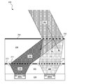
도 2는 예시의 집적된 서브-파장 격자 시스템(200)을 도시하는 도면이다. 특정한 예시의 예에 따라, 광전자 기판(226) 내에 다수의 광전자 콤포넌트(224)가 형성된다. 광전자 기판은 광전자 콤포넌트가 안에 형성되는 칩을 지칭한다. 광전자 기판층(226) 및 그 안에 형성된 광전자 콤포넌트(224)의 정부 상에 제1 투명층(222)이 형성된다. 제1 투명층(222)의 정부 상에 제1 격자층(212)이 형성된다. 제1 격자층은 광전자 콤포넌트(224)의 활성 영역과 정렬되는 상태로 형성된 다수의 서브-파장 격자 요소(214, 216)를 포함한다. 제1 격자층(212)의 정부 상에 제2 투명층(228)이 형성된다. 제2 투명층(228)의 정부 상에는 제2 격자층(204)이 형성된다. 제2 격자층(204)에는 회절 격자 요소(206)가 형성된다.FIG. 2 is a diagram illustrating an exemplary integrated sub-wavelength
광전자 기판(226)은 표준 집적회로 제조 공정에서 사용되는 표준 반도체 재료이어도 된다. 투명층(222, 228)은 그 재료를 통한 광 주파수에서의 전자기 방사선의 전파를 허용하는 어떠한 재료로도 이루어질 수 있다. 예컨대, 투명층(222, 228)은 산화물 재료로 이루어질 수도 있다.The
도 2에 도시된 예에서, 광전자 콤포넌트(224)는 광검출 디바이스이다. 그러므로, 격자 시스템은 디멀티플렉서로서 동작한다. 특정한 예시의 예에 따라, 광의 빔(202)은 회절 격자(206)에 입사된다. 이 광의 빔(202)은 복수 파장의 광을 포함할 수도 있다. 광의 빔이 회절 격자 요소(206)에 충돌할 때, 이 광의 빔은 회절 격자 요소(206)의 다른 면 상의 파장에 따라 분리될 것이다.In the example shown in FIG. 2, the optoelectronic component 224 is a photodetecting device. Therefore, the lattice system operates as a demultiplexer. According to a specific example, a beam of
회절 격자는 불투명 재료에 다수의 주기적 개구부를 포함한다. 그러므로, 광은 이들 개구부에서만 회절 격자를 통과하도록 허용된다. 각각의 이들 개구부는 근본적으로 광이 충돌하는 면의 반대 면에 대한 점 소스(point source)로서 동작한다. 회절 격자의 출력 면 상의 임의의 점에서의 광의 파면(wavefront)은 각각의 개구부를 통과하는 광의 조합이 된다. 이들 파는 특정한 방향이 각각의 개구부로부터의 광의 가중(summation)에 의해 최대 세기에 있게 되도록 하는 방식으로 보강적으로 또는 상쇄적으로 상호작용할 것이다. 어느 각도가 근본적으로 광의 빔을 전파할지를 설명하는 수식은 다음과 같다:The diffraction grating includes a plurality of periodic openings in the opaque material. Therefore, light is allowed to pass through the diffraction grating only in these openings. Each of these openings basically acts as a point source for the opposite surface of the surface where the light impinges. The wavefront of the light at an arbitrary point on the output surface of the diffraction grating is a combination of the lights passing through the respective openings. These waves will interact either reinforce or offset in such a way that a particular direction is at maximum intensity by summation of light from each aperture. The formula describing which angle will fundamentally propagate the beam of light is:
d(sin(Tm) - sin(Ti)) = mλ (수식 1) d (sin (T m) - sin (T i)) = mλ ( Equation 1)
여기서,here,
d = 회절 격자의 개구부의 직경d = diameter of the opening of the diffraction grating
Tm = 광이 최대치가 되는 각도T m = angle at which light is maximum
Ti = 광이 회절 격자에 입사하는 각도T i = angle at which light enters the diffraction grating
m = 정수, 및m = integer, and
λ = 입사광의 파장λ = wavelength of incident light
상기한 수식으로부터 알 수 있는 바와 같이, 상이한 파장은 회절 격자 요소로부터의 상이한 각도에서 최대치를 가질 것이다. 그러므로, 복수 파장의 광을 포함하는 광의 입사빔(202)이 회절 격자 요소(206)에 입사하면, 광의 상이한 파장이 회절 격자 요소(206)의 다른 면 상에서 상이한 각도로 지향될 것이다. 이 예에서, 광의 빔은 광의 2개의 파장을 포함한다. 광의 빔(202)이 회절 격자 요소(206)를 통과할 때, 하나의 파장의 광의 제1 빔(208)은 하나의 각도로 제2 투명층(228)을 통해 전파하는 한편, 상이한 파장의 광의 제2 빔(210)은 상이한 각도로 제2 투명층(228)을 통해 전파한다.As can be seen from the above equations, the different wavelengths will have a maximum at different angles from the diffraction grating element. Therefore, when the
서브-파장 격자(216)에 관련한 회절 격자(206)의 배치는 광의 빔(208, 210)이 이들 빔의 기지의 파장(known wavelength)에 기초하여 이들 서브-파장 격자(214, 216)를 향해 지향되도록 이루어진다. 이에 부가하여, 서브-파장 격자에 입사될 빔의 기지의 파장에 기초하여, 서브-파장 격자는 적절한 각도로부터의 광을 직접 광검출 광 콤포넌트(224)를 향해 방향 전환하도록 설계될 수 있다.The arrangement of the
예컨대, 제1 서브-파장 격자(214)는 특정 각도로부터 인입하는 광을 광전자 콤포넌트(224-1)를 향해 지향시키도록 설계될 수도 있다. 구체적으로, 광빔(208)이 서브-파장 격자(214)를 통과할 때, 이 광빔은 광검출 광전자 콤포넌트(224-1)의 활성 영역을 목표로 하는 포커싱된 빔(218)이 될 것이다. 마찬가지로, 다른 서브-파장 격자(216)를 통과하는 광의 빔(210)은 다른 광검출 광전자 콤포넌트(224-2)의 활성 영역을 향해 지향된 포커싱된 빔(220)이 될 것이다. 이러한 방식으로, 상이한 광전자 콤포넌트(224)는 동일한 광전송 매체를 통해 동시에 전파될 수 있는 상이한 데이터 스트림과 함께 작동할 수 있다.For example, the first
도 3은 서브-파장 격자 요소(300)의 예시의 평면도를 도시하는 도면이다. 이러한 서브-파장 격자 요소는 전술한 바와 같이 이용될 수 있다(예컨대, 도 2에서의 214 및 216). 특정한 예시의 예에 따라, 서브-파장 격자 요소(300)는 격자층(310)에 형성된 2차원 패턴이다. 격자층(310)은 규소 또는 게르마늄과 같은 단일 원소 반도체로 구성될 수도 있다. 이와 달리, 격자층은 Ⅲ-Ⅴ 반도체와 같은 화합물 반도체로 구성될 수 있다. 로마 숫자 Ⅲ과 Ⅴ는 원소 주기율표의 Ⅲa 열과 Ⅴa 열의 원소를 나타낸다.3 is a top view of an exemplary sub-wavelength
전술한 바와 같이, 격자층(310)은 투명층의 정부 상에 형성된다. 격자층(310) 재료는 아래의 투명층보다 높은 굴절률을 갖도록 선택될 수 있다. 격자층과 투명층 간의 이러한 비교적 높은 굴절률의 차이에 의해, 서브-파장 격자 요소는 하이-콘트라스트 서브-파장 격자 요소로서 지칭될 수 있다.As described above, the
격자 패턴은 상보형 금속 산화물 반도체(CMOS) 호환 기술을 이용하여 서브-파장 격자 요소를 형성하기 위해 격자층(310)에 형성될 수 있다. 예컨대, 서브-파장 격자 요소(300)는 웨이퍼 본딩 또는 화학적 또는 물리적 기상 증착을 이용하여 투명층의 평면 표면 상에 격자층(310)을 침적함으로써 제조될 수 있다. 그리고나서, 포토리소그래피 기술을 이용하여 격자층(310)의 일부분을 제거함으로써 그 아래의 투명층(304)을 노출시킬 수 있다. 격자층(310)의 일부분을 제거하는 것은 다수의 격자 특징부(302)가 남도록 할 것이다. 도 3의 예에서, 격자 특징부(302)는 포스트(post)이다. 그러나, 몇몇 경우에, 격자 특징부는 홈(groove)이어도 된다.The grating pattern may be formed in the
격자 특징부(302)들의 중심 간 거리는 격자 상수(308)로서 지칭된다. 격자 상수(308)는 서브-파장 격자 요소가 원하지 않는 방식으로 광을 산란시키지 않도록 선택된다. 원하지 않은 산란은 격자 상수를 적절하게 선택함으로써 방지될 수 있다. 서브-파장 격자는 또한 주기적이지 않아도 된다. 즉, 포스트의 직경 또는 홈의 폭과 같은 격자 특징부의 파라미터는 서브-파장 격자 요소(300)의 영역을 가로질러 변동될 수도 있다. 격자 특징부(302)의 치수(306) 및 격자 상수(308)의 길이 둘 모두는 서브-파장 격자 요소를 통해 진행하는 VCSEL에 의해 생성된 광의 파장보다 작다.The center-to-center distance of the grid features 302 is referred to as the
격자 상수(308) 및 격자 특징부 파라미터는 서브-파장 격자 요소(300)가 특정한 기능을 수행하도록 이루어질 수 있도록 선택될 수 있다. 예컨대, 서브-파장 격자 요소(300)는 특정한 방식으로 광을 포커싱하도록 설계될 수 있다. 이와 달리, 서브-파장 격자 요소(300)는 광을 시준하도록 설계될 수도 있다. 이에 부가하여, 서브-파장 격자 요소는 시준된 빔을 특정한 각도로 기울어지게 할 수도 있다. 몇몇 경우에, 서브-파장 격자 요소는 광의 빔을 스플리트하거나 굽어지게 할 수도 있다. 특정한 기능을 위한 이러한 서브-파장 격자 요소를 설계하는 방법에 대한 더욱 세부적인 내용은 예컨대 2011년 10월 27일자로 공개된 미국 특허 공개 번호 2011-0261856에 기술되어 있다.The lattice constant 308 and the grating feature parameter may be selected such that the sub-wavelength
도 4는 멀티플렉서(400)로서 사용된 예시의 집적된 서브-파장 격자 시스템을 도시하는 도면이다. 전술한 바와 같이, 광 멀티플렉서는 상이한 파장의 상이한 광신호를 동일한 광전송 매체 내로 조합하여 이들 신호가 매체를 통해 동시에 전파할 수 있도록 하기 위해 이용될 수 있다.FIG. 4 is a diagram illustrating an example integrated sub-wavelength grating system used as a
특정한 예시의 예에 따라, VCSEL과 같은 복수 광원(402)은 상이한 파장의 광을 투사하도록 설계된다. VCSEL(402)로부터의 광의 빔은 서브-파장 격자의 어레이(404)를 향해 투사된다. 그 어레이 내의 각각의 서브-파장 격자는 대응하는 VCSEL로부터의 광을 투명 매체(406)를 통해 단일 점을 향해 지향시키도록 특별하게 정렬되고 설계된다. 그 단일 점에서, 회절 격자의 어레이(408)로부터의 회절 격자가 그 광을 모아서 광전송 매체(410)를 향해 지향시킬 것이다.According to a specific example, a plurality of light sources 402, such as VCSELs, are designed to project light of different wavelengths. The beam of light from the VCSEL 402 is projected toward the
도 5는 디멀티플렉서(500)로서 사용된 예시의 집적된 서브-파장 격자 시스템을 도시하는 도면이다. 전술한 바와 같이, 광 디멀티플렉서는 광의 빔을 파장에 따라 분할한다. 그러므로, 단일 광전송 매체 내로 조합되는 상이한 파장을 갖는 광의 빔이 추가의 처리를 위해 분리될 수 있다.FIG. 5 is a diagram illustrating an example integrated sub-wavelength grating system used as
특정한 예시의 예에 따라, 복수-파장 광의 빔이 광전송 매체(502)의 밖으로 나갈 때, 이 빔은 회절 격자(504)를 향해 투사된다. 회절 격자는 파장에 따라 광을 분할하도록 설계된다. 광의 각각의 분리된 빔은 투명 매체(510)를 통해 전파된 후에 서브-파장 격자 요소의 어레이(506)의 서브-파장 격자 요소에 도달한다. 이들 서브-파장 격자 요소는 그 후 자신의 각자의 광빔을 광전자 검출기 디바이스(508)의 어레이를 향해 포커싱한다.According to a specific example, when the beam of multi-wavelength light exits the
몇몇 경우에, 광의 복수의 파장은 비교적 작은 차이로 될 수도 있다. 그러므로, 회절 격자를 통과할 때의 광의 각각의 빔에 대한 각도의 차이는 비교적 작게 될 수 있다. 이들 빔이 충분히 분리되어 이들 빔이 상이한 광요소를 향해 투사되도록 하기 위해, 회절 격자 요소와 서브-파장 격자 요소 사이의 투명층이 상대적으로 두껍게 될 수도 있다. 그러나, 가능한 가장 적은 양의 공간을 차지하도록 회로 및 칩을 설계하는 공통적인 목적에 의해, 이와 같이 두껍게 하는 것은 바람직하지 않을 것이다. 이하에서는 별개의 빔들 간의 파장의 차이가 비교적 작은 각도 확산을 산출하는 때에도 비교적 얇은 투명층을 이용하는 방법을 설명한다.In some cases, the plurality of wavelengths of light may be a relatively small difference. Therefore, the difference in angle of each beam of light when passing through the diffraction grating can be made relatively small. The transparent layer between the diffraction grating element and the sub-wavelength grating element may be relatively thick so that these beams are sufficiently separated so that they are projected towards different light elements. However, due to the common purpose of designing the circuit and chip to occupy the smallest possible amount of space, such thickening would not be desirable. Hereinafter, a method of using a relatively thin transparent layer is also described, even when the difference in wavelength between the different beams is relatively small.
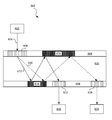
도 6은 각도 확산을 증가시키기 위해 이용된 얇은 투명층 및 반사성 표면을 갖는 예시의 집적된 서브-파장 격자 시스템(600)을 도시하는 도면이다. 특정한 예시의 예에 따라, 광의 복수-파장 빔(604)이 광전송 매체(602)로부터 제2 격자층(608) 내에 형성된 회절 격자 요소(606)에 투사된다. 회절 격자 요소(606)는 광의 복수-파장 빔이 파장에 따라 스플리트되도록 한다. 이 예에서, 스플리트는 상이한 파장의 광의 2개의 빔(610, 612)을 발생한다.FIG. 6 is a diagram illustrating an exemplary integrated sub-wavelength
투명층(620)의 비교적 얇은 성질에 의해, 2개의 빔(610, 612)은 이들이 제1 격자층(618)에 도달하는 시간에 의해서는 충분히 떨어져 확산되지 않는다. 그러므로, 투명층(620)을 통해 이들 광빔을 역반사하기 위해 제1 격자층(618) 내에 반사성 요소(614)가 형성된다. 이에 부가하여, 광빔을 투명층(620)을 통해 제1 격자층(618)을 향해 반대로 바운스(bounce)하기 위해 제2 격자층(608) 내에 또 다른 반사성 요소(616)가 형성된다.Due to the relatively thin nature of the
광은 입사하는 각도와 동일한 각도로 반사성 표면으로부터 반사된다. 그러므로, 광이 투명층(620)을 통해 왔다갔다 바운스됨에 따라 각도 확산은 일정하게 유지될 것이다. 몇몇 예에서, 광빔(610, 612)은 제1 격자층(618) 내에 형성된 서브-파장 격자 요소(622, 624)에 도달하기 전에 왔다갔다 여러 번 바운스될 수도 있다.The light is reflected from the reflective surface at an angle equal to the incident angle. Therefore, the angular spreading will remain constant as the light is bounced back and forth through the
서브-파장 격자 요소(622, 624)에 도달할 시에, 각각의 광빔은 대응하는 광전자 콤포넌트를 향해 적절하게 방향 전환되고 포커싱될 것이다. 예컨대, 제1 서브-파장 격자(622)는 광을 제1 빔(612)이 수광되는 각도로부터 제1 광전자 콤포넌트(626) 쪽으로 지향시키도록 설계된다. 마찬가지로, 제2 서브-파장 격자(624)는 광을 제2 빔(610)이 수광되는 각도로부터 제2 광전자 콤포넌트(628) 쪽으로 지향시키도록 설계된다.Upon reaching sub-wavelength
반사성 요소를 형성하기 위해 다양한 재료가 이용될 수 있다. 몇몇 경우에, 격자층의 일부분이 에칭으로 제거되고, 반사성 층으로 채워질 수 있다. 몇몇 경우에, 격자층이 배치되기 전에 투명층 상에 반사성 물질이 배치될 수도 있다. 몇몇 경우에, 특정한 반사성 요소가 형성되지 않고, 광이 내부 전반사에 기초하여 바운스된다. 내부 전반사는 광이 표면에 법선을 이루는 벡터에 대한 특정한 임계각보다 큰 각도로 매체 경계를 때리는 프로세스를 지칭한다. 굴절률이 경계의 다른 면 상에서보다 낮고, 입사각이 임계각보다 크다면, 모든 광이 반사될 것이다. 이 경우, 투명층의 경계 외측의 재료가 투명 재료보다 낮은 굴절률을 갖는다면, 입사각이 임계각보다 크게 되는 한, 광은 내부에서 반사될 것이다.A variety of materials can be used to form the reflective element. In some cases, a portion of the grating layer may be removed by etching and filled with a reflective layer. In some cases, the reflective material may be disposed on the transparent layer before the grating layer is disposed. In some cases, no specific reflective element is formed, and light is bounced based on total internal reflection. Internal total reflection refers to a process in which light hits the media boundary at an angle greater than a particular critical angle for a vector normal to the surface. If the index of refraction is lower on the other side of the boundary and the angle of incidence is greater than the critical angle, all light will be reflected. In this case, if the material outside the boundary of the transparent layer has a lower refractive index than the transparent material, the light will be reflected internally as long as the angle of incidence is greater than the critical angle.
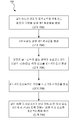
도 7은 집적된 서브-파장 격자 시스템을 형성하는 예시의 방법을 도시하는 흐름도(700)이다. 특정한 예시의 예에 따라, 본 방법은, 2개 이상의 광전자 콤포넌트를 포함하는 광전자 기판층 상에 제1 투명층을 형성하는 단계(단계 702)와, 제1 투명층 상에 제1 격자층을 형성하는 단계(단계 704)와, 광전자 콤포넌트의 활성 영역과 정렬되는 2개 이상의 서브-파장 격자 요소를 제1 격자층에 형성하는 단계(단계 706)와, 제1 격자층으로부터 거리를 두고 제2 격자를 형성하는 단계(단계 708)와, 광이 회절 격자와 2개 이상의 서브-파장 격자 요소 사이에서 전파되도록 정렬된 회절 격자 요소를 제2 격자층에 형성하는 단계(단계 710)를 포함한다.FIG. 7 is a flow diagram 700 illustrating an exemplary method of forming an integrated sub-wavelength grating system. According to a specific example, the method includes forming a first transparent layer on an optoelectronic substrate layer comprising two or more optoelectronic components (step 702), forming a first grating layer on the first transparent layer (Step 704), forming two or more sub-wavelength grating elements in the first grating layer that are aligned with active areas of the optoelectronic component (step 706), forming a second grating at a distance from the first grating layer (Step 708), and forming (step 710) a diffraction grating element in the second grating layer so that light is propagated between the diffraction grating and the two or more sub-wavelength grating elements.
결론으로, 본 명세서에 개시된 원리를 구현하는 시스템 및 방법을 이용함으로써, 집적된 칩 상에 모노리식 방식으로 멀티플렉싱 및 디멀티플렉싱 시스템이 형성될 수 있다. 그러므로, 복잡한 렌즈 시스템 및 정렬 공정을 이용하지 않아도 된다. 이러한 시스템은 보다 비용이 덜 들고 보다 소형의 광전송 시스템을 가능하게 한다.In conclusion, by using systems and methods that implement the principles disclosed herein, a multiplexing and demultiplexing system can be formed in a monolithic manner on an integrated chip. Therefore, a complicated lens system and alignment process need not be used. These systems enable less costly and smaller optical transmission systems.
이상의 설명은 개시된 원리의 예를 예시하고 설명하기 위해 제공된 것이다. 이러한 설명은 모든 것을 망라하여 나타내거나 또는 이들 원리를 개시된 정밀한 형태로 한정하려는 것은 아니다. 상기한 교시에 비추어 다수의 수정예 및 변형예가 가능하다.The foregoing description is provided to illustrate and describe examples of the principles disclosed. This description is not intended to be exhaustive or to limit the principles to the precise forms disclosed. Many modifications and variations are possible in light of the above teachings.
Claims (15)
2개 이상의 광전자 콤포넌트를 포함하는 광전자 기판층 상에 형성된 제1 투명층;
상기 제1 투명층 상에 배치되고, 상기 광전자 콤포넌트의 활성 영역과 정렬되는 상태로 형성된 2개 이상의 서브-파장 격자 요소를 포함하는 제1 격자층; 및
광이 제2 격자층 내에 형성된 회절 격자 요소와 상기 2개 이상의 서브-파장 격자 요소 사이에서 전파되도록 상기 제1 격자층으로부터 거리를 두고 있는 제2 격자층
을 포함하는 집적된 격자 요소 시스템.In an integrated lattice element system,
A first transparent layer formed on an optoelectronic substrate layer comprising two or more optoelectronic components;
A first grating layer disposed on the first transparent layer and including at least two sub-wavelength grating elements formed in alignment with active areas of the optoelectronic component; And
And a second grating layer spaced from the first grating layer to propagate between the at least two sub-wavelength grating elements and a diffraction grating element formed in the second grating layer,
≪ / RTI >
상기 제1 격자층과 상기 제2 격자층 간의 상기 거리에는 제2 투명층이 포함되어 있는, 집적된 격자 요소 시스템.The method according to claim 1,
And wherein a second transparent layer is included at the distance between the first grating layer and the second grating layer.
상기 제1 격자층과 상기 제2 격자층 사이의 광을 상기 회절 격자 요소와 상기 서브-파장 격자 요소 사이에서 바운스(bounce)하도록 위치되는 반사성 표면을 더 포함하는, 집적된 격자 요소 시스템.The method according to claim 1,
And a reflective surface positioned to bounce light between the first grating layer and the second grating layer between the diffraction grating element and the sub-wavelength grating element.
상기 2개 이상의 광전자 콤포넌트는 상이한 파장의 광을 상기 서브-파장 격자 요소에 투사하기 위해 광원을 포함하는, 집적된 격자 요소 시스템.The method according to claim 1,
Wherein the at least two optoelectronic components comprise a light source for projecting light of different wavelengths to the sub-wavelength grating element.
상기 서브-파장 격자 요소는 상기 광원으로부터 투사된 광을 상기 제2 격자층 내에 형성된 상기 회절 격자 요소 쪽으로 시준하고 각을 이루도록 하는, 집적된 격자 요소 시스템.5. The method of claim 4,
Wherein the sub-wavelength grating element collimates and angles the light projected from the light source towards the diffraction grating element formed in the second grating layer.
상기 2개 이상의 광전자 콤포넌트는 상기 서브-파장 격자 요소로부터 상이한 파장의 광을 수광하기 위해 광검출기 디바이스를 포함하는, 집적된 격자 요소 시스템.The method according to claim 1,
Wherein the at least two optoelectronic components comprise a photodetector device for receiving light of a different wavelength from the sub-wavelength grating element.
상기 회절 격자 요소는 입사광을 파장에 따라 복수 방향으로 스플리트(split)하며, 상기 방향이 상기 서브-파장 격자 요소를 가리키는, 집적된 격자 요소 시스템.The method according to claim 6,
Wherein the diffraction grating element splits the incident light in multiple directions along the wavelength and the direction points to the sub-wavelength grating element.
상기 서브-파장 격자 요소는 사전에 정해진 방식으로 광에 영향을 미치기 위해 격자 특징부 파라미터의 2차원의 비주기적 변동을 포함하는, 집적된 격자 요소 시스템.The method according to claim 1,
Wherein the sub-wavelength grating element comprises a two-dimensional aperiodic variation of the grating feature sub-parameters to affect light in a predetermined manner.
2개 이상의 광전자 콤포넌트를 포함하는 광전자 기판층 상에 제1 투명층을 형성하는 단계;
상기 제1 투명층 상에 제1 격자층을 형성하는 단계;
상기 광전자 콤포넌트의 활성 영역과 정렬되는 2개 이상의 서브-파장 격자 요소를 상기 제1 격자층에 형성하는 단계;
상기 제1 격자층으로부터 거리를 두고 제2 격자를 형성하는 단계; 및
광이 회절 격자와 상기 2개 이상의 서브-파장 격자 요소 사이에서 전파되도록 정렬된 회절 격자 요소를 상기 제2 격자층에 형성하는 단계
를 포함하는, 집적된 서브-파장 격자 시스템을 형성하는 방법.A method of forming an integrated sub-wavelength grating system,
Forming a first transparent layer on the optoelectronic substrate layer comprising two or more optoelectronic components;
Forming a first grating layer on the first transparent layer;
Forming at least two sub-wavelength grating elements in the first grating layer that are aligned with an active region of the optoelectronic component;
Forming a second grating at a distance from the first grating layer; And
Forming in the second grating layer a diffraction grating element arranged such that light propagates between the diffraction grating and the at least two sub-wavelength grating elements,
/ RTI > The method of claim 1,
상기 제1 격자층과 상기 제2 격자층 사이의 광을 상기 회절 격자 요소와 상기 서브-파장 격자 요소 사이에서 반사하는 단계를 더 포함하는, 집적된 서브-파장 격자 시스템을 형성하는 방법.10. The method of claim 9,
And reflecting light between the first grating layer and the second grating layer between the diffraction grating element and the sub-wavelength grating element. ≪ Desc / Clms Page number 21 >
상기 2개 이상의 광전자 콤포넌트는 상이한 파장의 광을 상기 서브-파장 격자 요소에 투사하기 위해 광원을 포함하는, 집적된 서브-파장 격자 시스템을 형성하는 방법.10. The method of claim 9,
Wherein the at least two optoelectronic components comprise a light source for projecting light of different wavelengths to the sub-wavelength grating element.
상기 서브-파장 격자 요소로, 상기 광원으로부터의 광을 상기 회절 격자 요소 쪽으로 시준하고 기울어지게 하는 단계를 더 포함하는, 집적된 서브-파장 격자 시스템을 형성하는 방법.12. The method of claim 11,
Further comprising collimating and tilting light from the light source toward the diffraction grating element with the sub-wavelength grating element. ≪ Desc / Clms Page number 19 >
상기 2개 이상의 광전자 콤포넌트는 상기 서브-파장 격자 요소로부터 상이한 파장의 광을 수광하기 위해 광검출기 디바이스를 포함하는, 집적된 서브-파장 격자 시스템을 형성하는 방법.10. The method of claim 9,
Wherein the at least two optoelectronic components comprise a photodetector device for receiving light of a different wavelength from the sub-wavelength grating element.
상기 회절 격자 요소로, 입사광을 파장에 따라 복수 방향으로 스플리트하는 단계를 더 포함하며, 상기 방향이 상기 서브-파장 격자 요소를 가리키는, 집적된 서브-파장 격자 시스템을 형성하는 방법.14. The method of claim 13,
Further comprising the step of splitting the incident light into a plurality of directions along the wavelength with the diffraction grating element, the direction being indicative of the sub-wavelength grating element.
집적회로 칩을 포함하며, 상기 집적회로 칩이,
광전자 콤포넌트의 어레이를 포함하는 광전자 기판층 상에 형성된 제1 투명층;
상기 제1 투명층 상에 배치되고, 상기 광전자 콤포넌트의 활성 영역과 정렬되는 상태로 형성된 2개의 서브-파장 격자 요소의 어레이를 포함하는 제1 격자층;
상기 제1 격자층 상에 형성된 제2 투명층; 및
상기 제2 투명층 상에 형성되며, 회절 격자 요소의 어레이를 포함하며, 각각의 상기 회절 격자 요소가, 상이한 파장의 2개 이상의 상기 서브-파장 격자 요소 사이의 광을 커플링하도록 구성되는, 제2 격자층
을 포함하는, 집적된 서브-파장 격자 요소 시스템.In an integrated sub-wavelength lattice element system,
An integrated circuit chip, comprising:
A first transparent layer formed on an optoelectronic substrate layer comprising an array of optoelectronic components;
A first grating layer disposed on the first transparent layer and comprising an array of two sub-wavelength grating elements formed in alignment with an active region of the optoelectronic component;
A second transparent layer formed on the first grating layer; And
A second grating element formed on the second transparent layer and including an array of diffraction grating elements, each diffraction grating element being configured to couple light between two or more of the sub-wavelength grating elements of different wavelengths; Lattice layer
/ RTI > of claim 1, wherein the integrated sub-
Applications Claiming Priority (1)
| Application Number | Priority Date | Filing Date | Title |
|---|---|---|---|
| PCT/US2012/021066 WO2013105959A1 (en) | 2012-01-12 | 2012-01-12 | Integrated sub-wavelength grating system |
Publications (1)
| Publication Number | Publication Date |
|---|---|
| KR20140112012A true KR20140112012A (en) | 2014-09-22 |
Family
ID=48781764
Family Applications (1)
| Application Number | Title | Priority Date | Filing Date |
|---|---|---|---|
| KR1020147015966A KR20140112012A (en) | 2012-01-12 | 2012-01-12 | Integrated sub-wavelength grating system |
Country Status (5)
| Country | Link |
|---|---|
| US (1) | US9612402B2 (en) |
| EP (1) | EP2803123B1 (en) |
| KR (1) | KR20140112012A (en) |
| CN (1) | CN103999303B (en) |
| WO (1) | WO2013105959A1 (en) |
Families Citing this family (16)
| Publication number | Priority date | Publication date | Assignee | Title |
|---|---|---|---|---|
| CN103999304A (en) * | 2012-01-18 | 2014-08-20 | 惠普发展公司,有限责任合伙企业 | Integrated sub-wavelength grating element |
| WO2014168619A1 (en) * | 2013-04-11 | 2014-10-16 | Hewlett-Packard Development Company, L.P. | Mode conversion for optical isolation |
| EP2999980B1 (en) | 2013-05-22 | 2021-09-29 | Hewlett Packard Enterprise Development LP | Optical devices including a high contrast grating lens |
| WO2015065344A1 (en) * | 2013-10-29 | 2015-05-07 | Hewlett-Packard Development Company, L.P. | High contrast grating optoelectronics |
| US10082684B2 (en) | 2014-01-24 | 2018-09-25 | Hewlett Packard Enterprise Development Lp | Optical modulation employing high contrast grating lens |
| CN106129789B (en) * | 2016-08-31 | 2019-03-12 | 南方科技大学 | Optical fiber laser |
| WO2018191491A1 (en) * | 2017-04-12 | 2018-10-18 | Sense Photonics, Inc. | Emitter structures for ultra-small vertical cavity surface emitting lasers (vcsels) and arrays incorporating the same |
| FR3077652B1 (en) * | 2018-02-05 | 2022-05-27 | Commissariat Energie Atomique | PHOTONIC CHIP WITH INTEGRATED COLLIMATING STRUCTURE |
| WO2019207438A1 (en) * | 2018-04-26 | 2019-10-31 | SM Optics S.r.l. | Optical device for demultiplexing and multiplexing modes with different orbital angular momentum |
| CN110764186B (en) * | 2018-07-27 | 2022-02-22 | 京东方科技集团股份有限公司 | Optical waveguide substrate and microfluidic device |
| US11344884B2 (en) | 2018-07-26 | 2022-05-31 | Boe Technology Group Co., Ltd. | Microfluidic apparatus, method of detecting substance in microfluidic apparatus, and spectrometer |
| CN109038216B (en) * | 2018-10-29 | 2023-10-31 | 厦门乾照半导体科技有限公司 | Multi-beam vertical cavity surface emitting laser chip and manufacturing method thereof |
| US10795098B2 (en) * | 2018-12-21 | 2020-10-06 | Hewlett Packard Enterprise Development Lp | Mode division multiplexing using vertical-cavity surface emitting lasers |
| US20210132196A1 (en) * | 2019-11-06 | 2021-05-06 | Lookit.ai | Flat optics with passive elements functioning as a transformation optics and a compact scanner to cover the vertical elevation field-of-view |
| CN115210619A (en) * | 2020-01-31 | 2022-10-18 | 康宁股份有限公司 | Wavelength multiplexer/demultiplexer using metamaterials for optical fiber communication |
| CN115201970B (en) * | 2022-07-13 | 2023-10-20 | 北京摩尔芯光半导体技术有限公司 | Silicon-based optical chip with grating coupler |
Family Cites Families (23)
| Publication number | Priority date | Publication date | Assignee | Title |
|---|---|---|---|---|
| US4994664A (en) * | 1989-03-27 | 1991-02-19 | Massachusetts Institute Of Technology | Optically coupled focal plane arrays using lenslets and multiplexers |
| US4944664A (en) * | 1989-09-19 | 1990-07-31 | Allred Cecil F | Concrete wall form apparatus |
| US5061027A (en) * | 1990-09-04 | 1991-10-29 | Motorola, Inc. | Solder-bump attached optical interconnect structure utilizing holographic elements and method of making same |
| EP0746783B1 (en) * | 1993-02-26 | 2003-04-16 | Yeda Research & Development Company, Ltd. | Holographic optical devices |
| JP3119540B2 (en) | 1993-04-12 | 2000-12-25 | 松下電器産業株式会社 | Light tap |
| US5731874A (en) * | 1995-01-24 | 1998-03-24 | The Board Of Trustees Of The Leland Stanford Junior University | Discrete wavelength spectrometer |
| US20030002789A1 (en) * | 2000-10-31 | 2003-01-02 | Boye Robert R. | Integrated optical coupler |
| US6490393B1 (en) | 2000-11-27 | 2002-12-03 | Advanced Interfaces, Llc | Integrated optical multiplexer and demultiplexer for wavelength division transmission of information |
| US7050675B2 (en) | 2000-11-27 | 2006-05-23 | Advanced Interfaces, Llc | Integrated optical multiplexer and demultiplexer for wavelength division transmission of information |
| US6782027B2 (en) * | 2000-12-29 | 2004-08-24 | Finisar Corporation | Resonant reflector for use with optoelectronic devices |
| US7177496B1 (en) * | 2001-12-27 | 2007-02-13 | Capella Photonics, Inc. | Optical spectral power monitors employing time-division-multiplexing detection schemes |
| JP3949977B2 (en) * | 2002-02-18 | 2007-07-25 | 沖電気工業株式会社 | Wavelength division multiplexing optical demultiplexer |
| JPWO2004027493A1 (en) | 2002-09-20 | 2006-01-19 | 日本板硝子株式会社 | Spectrometer using diffraction grating |
| JP2004226901A (en) * | 2003-01-27 | 2004-08-12 | Ricoh Co Ltd | Wavelength multiplexer/demultiplexer and its manufacturing method |
| JP4425059B2 (en) | 2003-06-25 | 2010-03-03 | シャープ株式会社 | Polarizing optical element and display device using the same |
| EP1691224A1 (en) | 2005-02-10 | 2006-08-16 | Konica Minolta Opto, Inc. | Diffractive grating member and optical communication module |
| US7460231B2 (en) | 2006-03-27 | 2008-12-02 | Asml Netherlands B.V. | Alignment tool for a lithographic apparatus |
| TWI354809B (en) | 2008-06-24 | 2011-12-21 | Ind Tech Res Inst | Composite optical dividing device |
| US8400537B2 (en) * | 2008-11-13 | 2013-03-19 | Omnivision Technologies, Inc. | Image sensors having gratings for color separation |
| WO2010140998A1 (en) | 2009-06-02 | 2010-12-09 | Vladimir Yankov | Optical integrated nanospectrometer and method of manufacturing thereof |
| WO2011081692A2 (en) | 2009-10-06 | 2011-07-07 | Sri International | Twin sub-wavelength grating optical signal processor |
| WO2011106553A2 (en) * | 2010-02-24 | 2011-09-01 | The Regents Of The University Of California | Planar, low loss transmitting or reflecting lenses using sub-wavelength high contrast grating |
| CN102073103B (en) * | 2010-11-22 | 2013-11-13 | 北京交通大学 | Subwavelength binary diffraction grating-based wavelength separator |
-
2012
- 2012-01-12 WO PCT/US2012/021066 patent/WO2013105959A1/en active Application Filing
- 2012-01-12 CN CN201280061237.XA patent/CN103999303B/en active Active
- 2012-01-12 KR KR1020147015966A patent/KR20140112012A/en not_active Application Discontinuation
- 2012-01-12 EP EP12864761.7A patent/EP2803123B1/en active Active
- 2012-01-12 US US14/364,702 patent/US9612402B2/en active Active
Also Published As
| Publication number | Publication date |
|---|---|
| EP2803123A1 (en) | 2014-11-19 |
| US9612402B2 (en) | 2017-04-04 |
| US20150010271A1 (en) | 2015-01-08 |
| WO2013105959A1 (en) | 2013-07-18 |
| EP2803123A4 (en) | 2015-09-23 |
| CN103999303A (en) | 2014-08-20 |
| EP2803123B1 (en) | 2020-11-25 |
| CN103999303B (en) | 2018-03-13 |
Similar Documents
| Publication | Publication Date | Title |
|---|---|---|
| KR20140112012A (en) | Integrated sub-wavelength grating system | |
| US7376308B2 (en) | Optical off-chip interconnects in multichannel planar waveguide devices | |
| JP5645631B2 (en) | Wavelength monitor, optical module, and wavelength monitoring method | |
| US5477363A (en) | Optical switching device | |
| EP2062076B1 (en) | Method and system for grating taps for monitoring a dwdm transmitter array integrated on a plc platform | |
| US20160327746A1 (en) | Bidirectional optical multiplexing employing a high contrast grating | |
| JP2019168673A (en) | Photonic chip with integrated collimation structure | |
| KR20140112015A (en) | Integrated sub-wavelength grating element | |
| KR102110121B1 (en) | Optical slab | |
| US7587112B2 (en) | Optical device and light control method | |
| JP5983479B2 (en) | Optical element | |
| JP5599175B2 (en) | Dispersive element, spectroscopic device, and wavelength selective switch | |
| JPH11223745A (en) | Device equipped with virtual image phase array combined with wavelength demultiplexer for demultiplexing wavelength multiplexed light | |
| JP2009217247A (en) | Optical device provided with compact dispersing system | |
| KR20080029598A (en) | Optical fiber having diffraction grating, method of fabricating diffraction grating at cutting plane, and optical apparatus using the same fiber | |
| JP4330560B2 (en) | Optical demultiplexer and wavelength division multiplexing optical transmission module | |
| JP7293672B2 (en) | optical module | |
| JP2003066269A (en) | Multi-wavelength demultiplexing optical device and wavelength multiplexed light transmission module | |
| JPS63244003A (en) | Multiplexer/demultiplexer | |
| JP5312309B2 (en) | Optical multiplexer / demultiplexer | |
| TW486580B (en) | Planar optical waveguide type dense wavelength division multiplexer | |
| JP6303323B2 (en) | Optical device | |
| JP3611842B2 (en) | Manufacturing method of wavelength demultiplexer | |
| JP2000075165A (en) | Virtually imaged phased array having lens disposed in order to obtain broad beam width | |
| JP2018200959A (en) | Wavelength multiplexed transmitter optical module |
Legal Events
| Date | Code | Title | Description |
|---|---|---|---|
| N231 | Notification of change of applicant | ||
| A201 | Request for examination | ||
| E902 | Notification of reason for refusal | ||
| E601 | Decision to refuse application |