KR20140097714A - Mems catalytic type gas sensor using multi-holes membrane embedded micro-heater - Google Patents
Mems catalytic type gas sensor using multi-holes membrane embedded micro-heater Download PDFInfo
- Publication number
- KR20140097714A KR20140097714A KR1020130009883A KR20130009883A KR20140097714A KR 20140097714 A KR20140097714 A KR 20140097714A KR 1020130009883 A KR1020130009883 A KR 1020130009883A KR 20130009883 A KR20130009883 A KR 20130009883A KR 20140097714 A KR20140097714 A KR 20140097714A
- Authority
- KR
- South Korea
- Prior art keywords
- membrane
- gas sensor
- deposition method
- holes
- heat generating
- Prior art date
Links
Images


Classifications
-
- G—PHYSICS
- G01—MEASURING; TESTING
- G01N—INVESTIGATING OR ANALYSING MATERIALS BY DETERMINING THEIR CHEMICAL OR PHYSICAL PROPERTIES
- G01N27/00—Investigating or analysing materials by the use of electric, electrochemical, or magnetic means
- G01N27/02—Investigating or analysing materials by the use of electric, electrochemical, or magnetic means by investigating impedance
- G01N27/04—Investigating or analysing materials by the use of electric, electrochemical, or magnetic means by investigating impedance by investigating resistance
- G01N27/12—Investigating or analysing materials by the use of electric, electrochemical, or magnetic means by investigating impedance by investigating resistance of a solid body in dependence upon absorption of a fluid; of a solid body in dependence upon reaction with a fluid, for detecting components in the fluid
-
- G—PHYSICS
- G01—MEASURING; TESTING
- G01N—INVESTIGATING OR ANALYSING MATERIALS BY DETERMINING THEIR CHEMICAL OR PHYSICAL PROPERTIES
- G01N27/00—Investigating or analysing materials by the use of electric, electrochemical, or magnetic means
- G01N27/02—Investigating or analysing materials by the use of electric, electrochemical, or magnetic means by investigating impedance
- G01N27/04—Investigating or analysing materials by the use of electric, electrochemical, or magnetic means by investigating impedance by investigating resistance
- G01N27/14—Investigating or analysing materials by the use of electric, electrochemical, or magnetic means by investigating impedance by investigating resistance of an electrically-heated body in dependence upon change of temperature
- G01N27/16—Investigating or analysing materials by the use of electric, electrochemical, or magnetic means by investigating impedance by investigating resistance of an electrically-heated body in dependence upon change of temperature caused by burning or catalytic oxidation of surrounding material to be tested, e.g. of gas
Landscapes
- Chemical & Material Sciences (AREA)
- Physics & Mathematics (AREA)
- General Physics & Mathematics (AREA)
- General Health & Medical Sciences (AREA)
- Health & Medical Sciences (AREA)
- Life Sciences & Earth Sciences (AREA)
- Analytical Chemistry (AREA)
- Biochemistry (AREA)
- Electrochemistry (AREA)
- Chemical Kinetics & Catalysis (AREA)
- Immunology (AREA)
- Pathology (AREA)
- Investigating Or Analyzing Materials By The Use Of Electric Means (AREA)
- Investigating Or Analyzing Materials By The Use Of Fluid Adsorption Or Reactions (AREA)
- Engineering & Computer Science (AREA)
- Combustion & Propulsion (AREA)
Abstract
Description
본 발명의 실시 예는 MEMS형 접촉연소식 가스 센서에 관한 것으로, 더욱 상세하게는 다공성 멤브레인이 내장된 마이크로히터와 미세기전집적시스템(MEMS: Micro Electro Mechanical System) 기술을 이용한 접촉연소식 가스 센서에 관한 것이다.An embodiment of the present invention relates to a MEMS type contact combustion gas sensor and, more particularly, to a contact gas sensor using a micro heater with a porous membrane and a microelectromechanical system (MEMS) .
가스 센서에 대한 연구는 오래전부터 이루어져 왔다. 현재 광학식, 전기화학식, 반도체식, 접촉연소식, 표면 음향파(Surface Acoustic Wave) 방식 등의 다양한 방식의 가스 센서가 상용화되어 있다. 측정하고자 하는 가스의 스펙트럼의 변화나 이온 모빌리티(mobility)에 의한 전도성 측정을 통한 광학식 가스 센서나 전기 화학식 가스 센서, 감지 소재에 흡착된 가스로 인한 산화/환원 반응 등으로 인한 전도성 변화나 흡착된 가스에 의한 표면파 전송 속도 변화 측정을 통한 반도체식 가스 센서나 표면 음향파 방식 가스 센서에 비해 일반적으로 LPG/LNG 등의 메탄 계열의 가연성 감지소자용으로는 검지 대상인 이들 가스와 감지 소재와의 반응을 통해 발생하는 연소열에 의한 온도 변화를 측정함으로써 가연성 가스의 존재 여부와 농도를 결정하는 접촉연소식이 많이 사용돼 왔다.Gas sensors have been studied for a long time. Various types of gas sensors, such as optical, electric, semiconductor, contact combustion, surface acoustic wave, etc., have been commercialized. Conductivity changes due to changes in the spectrum of the gas to be measured, conductivity measurement by ion mobility, oxidation / reduction reaction due to gas adsorbed on the sensing material, optical gas sensor or electrochemical gas sensor, , It has been found that, in comparison with a semiconductor type gas sensor or a surface acoustic wave type gas sensor through the measurement of the surface wave transmission rate change by the change of the surface wave transmission rate, Contact combustion, which determines the presence and concentration of flammable gases by measuring the temperature change due to the heat of combustion, has been widely used.
도 1은 접촉연소식 가스 센서를 이용한 가연성 가스 감지 모듈의 구성도이다.1 is a configuration diagram of a combustible gas detection module using a contact combustion type gas sensor.
도 1에 도시된 바와 같이, 가연성 가스 감지 모듈(100)은 직류 전원(110), 가변 저항(Rv)(120), 고정 저항 1 및 2(R1 및 R2)(131 및 132), 감지 소자(Rd)(141) 및 보상 소자(Rc)(142)를 포함한다.1, the combustible
접촉연소식 가스 센서를 이용한 가연성 가스 감지 모듈(100)은 일반적으로 도 1과 같이 휘스톤 브릿지(Wheatstone Bridge) 회로로 구성되어 있다. 출력 전압(Vo)은 감지 소자(Rd)(141) 및 보상 소자(Rv)(142)의 연결 위치와 가변 저항(Rv)(120) 간의 전압을 나타낸다. 접촉연소식 가스 센서는 백금이나 팔라듐 같은 귀금속의 산화촉매를 첨가하여 만든 감지 소자(Rd)(141)와 가연성 가스의 산화가 일어나지 않도록 촉매를 첨가하지 않은 불활성의 보상 소자(Rc)(142)의 한 쌍으로 구성된다.The combustible
가연성 가스 감지 모듈(100)은 휘스톤 브릿지 회로의 특성을 이용하여 출력전압 Vo가 0이 되도록 가변저항을 보정한다. 가연성 가스가 주입되면, 가스와 감지 소재와의 반응을 통한 연소로 온도 변화가 발생한다. 이로 인한 저항의 변화로 가연성 가스 감지 모듈(100)에서의 휘스톤 브릿지 회로의 평형이 깨져 0이 아닌 Vo가 발생한다. 이값은 감지 소재의 촉매성능, 감지 소자(Rd)(141)의 열용량, 및 가연성 가스의 농도 등에 의존한다.The combustible
종래 접촉연소식 가스 센서 소자를 제작하는 방법은 알루미나나 쿼츠 등의 기판에 감지 소재와 감지 전극 그리고 감지 특성 향상을 위해 동작 온도를 올려주기 위한 히터가 있는 벌크형 접촉연소식 가스센서나, 다른 부분은 유사하지만 히터가 있는 부분을 식각 등의 방법으로 제거하여 열적으로 격리함으로써 소모 전력을 줄인 MEMS형 접촉연소식 가스 센서가 있다. Conventionally, a method of fabricating a contact-type gas sensor element is a bulk contact-type gas sensor having a sensing material and a sensing electrode on a substrate such as alumina or quartz and a heater for raising the operating temperature to improve the sensing property. There is a MEMS-type contact-fired gas sensor that reduces heat dissipation by thermally isolating and removing similar portions of the heater by etching or the like.
벌크형 접촉연소식 가스 센서는 갑작스런 충격에 강한 반면 감지 특성 향상을 위한 높은 동작 온도 유지를 위해 전력 소모가 큰 단점이 있어 휴대용 단말기나 USN 서비스용 센서 노드에의 적용이 어려웠다. 기존 MEMS형 접촉연소식 가스 센서는 발열 저항체 부분의 기판(주로 실리콘)을 식각함으로써 열적 격리를 하여 벌크형 접촉연소식 가스 센서에 비해 훨씬 적은 전력 소모가 장점이다. 그 방법상으로는 멤브레인들과 발열 저항체 부분을 남겨두고 그 뒷면의 기판을 식각하는 벌크 마이크로머시닝(Bulk Micromachining) 방법과 멤브레인들 일부분과 발열 저항체 부분을 남겨두고 그 뒷면의 기판을 일부분만 식각하는 표면 마이크로머시닝(Surface Micromachining) 방법으로 나누어진다. 그런데 전자는 멤브레인들이 뚫린 부분이 없이 기판과 연결되어 있으므로 상대적으로 기계적 강성을 가지지만 기판 두께만큼을 식각해야 하므로 공정 비용이 증가하는 단점이 있다. 후자의 경우 멤브레인들 일부분과 발열 저항체 부분을 남겨두고 그 뒷면의 기판 두께의 일부분만 식각하므로 공정 비용이 상대적으로 저렴하고 기판 뒷면이 닫혀있으므로 소자의 취급에도 용이하지만 멤브레인들에 뚫린 부분이 있는 상태로 기판과 연결되어 있으므로 상대적으로 약한 구조적 특성을 가진다. 하지만, 둘 다 구조적으로 갑작스런 충격에 상대적으로 약한 단점이 있다. Bulk type contact combustion gas sensor is strong against sudden impact, but has a disadvantage of high power consumption to maintain a high operating temperature for improving the sensing characteristic, making it difficult to apply it to a sensor node for a portable terminal or a USN service. Conventional MEMS type contact-fired gas sensors offer thermal isolation by etching the substrate (mainly silicon) of the heat-generating resistor part, which consumes much less power than a bulk contact-type gas sensor. The method includes a bulk micromachining method of etching the substrate on the backside with leaving the membranes and the heat generating resistor portion, a surface micromachining method in which a part of the membranes and the heat generating resistor portion are left, (Surface Micromachining) method. However, since electrons have relatively mechanical rigidity because they are connected to the substrate without having open portions of the membranes, there is a disadvantage in that the process cost is increased due to etching by the thickness of the substrate. In the latter case, since part of the membranes and the heat generating resistor are left and only a part of the substrate thickness on the back side is etched, the process cost is relatively inexpensive and the back surface of the substrate is closed, which facilitates handling of the device. It has relatively weak structural characteristics because it is connected to the substrate. However, they both have relatively weak disadvantages to sudden impacts on the structure.
그러나 휴대용 단말기 또는 유비쿼터스 센서 네트워크 등에서 탑재되어 다양한 서비스에 이용되기 위해서는 가능한 전력 소모가 적으면서도 갑작스런 충격에도 구조적/기계적/전기적으로 안정한 MEMS형 접촉연소식 가스 센서가 요구된다.However, in order to be used in various services installed in a portable terminal or a ubiquitous sensor network, there is a need for MEMS-type contact-fired gas sensor that is structurally, mechanically, and electrically stable even in a sudden shock while consuming less power.
따라서, 본 발명의 목적은, 멤브레인들, 발열 저항체 및 감지 전극에 다수의 구멍을 뚫고 그 구멍을 통해 기판의 일정 두께만큼 식각하여 열적으로 격리하고 감지 소재로 이루어진 감지 구조체와 보상 소재로 이루어진 보상 구조체를 포함함으로써, 초소형이면서 소모 전력이 현저히 줄어든 MEMS형 접촉연소식 가스 센서에서 구조적/기계적/전기적으로 안정하며 소자 제작 공정이 용이한 가스 센서를 제공하는 데에 있다.Accordingly, it is an object of the present invention to provide a compensation structure comprising a sensing structure made of a sensing material and a compensation material, which is thermally isolated by etching a plurality of holes in the membranes, the heat generating resistor and the sensing electrode, The present invention is to provide a gas sensor that is structurally, mechanically, and electrically stable and is easy to manufacture in a MEMS type contact combustion gas sensor that is very small and consumes significantly less power.
또한, 본 발명의 다른 목적은, 다양한 환경에서 서비스를 제공할 수 있는 접촉연소식 가스 센서를 제공하는 데에 있다.It is another object of the present invention to provide a contact-activated gas sensor capable of providing services in various environments.
그 외의 본 발명에서 제공하고자 하는 목적은, 하기의 설명 및 본 발명의 실시 예들에 의하여 파악될 수 있다.Other objects of the present invention can be understood by the following description and embodiments of the present invention.
이를 위하여, 본 발명의 일 실시 예에 따른 MEMS형 접촉연소식 가스 센서는, 다수의 구멍을 가진 제1 멤브레인; 상기 제1 멤브레인의 하부에 위치하되 하부면의 일부분과는 비접촉되도록 중앙 영역이 일정 두께만큼 식각된 기판; 상기 제1 멤브레인의 상면 중앙 영역에 형성되고 다수의 구멍을 가진 발열 저항체; 상기 제1 멤브레인과 상기 발열 저항체 위에 형성되고 다수의 구멍을 가진 제2 멤브레인; 상기 제2 멤브레인상의 중앙 영역에 형성되고 다수의 구멍을 가진 감지 전극; 상기 감지 전극 상에 가스 감지 소재로 형성된 하나 이상의 감지 구조체; 및 상기 감지 전극 상에 보상 소재로 형성된 하나 이상의 보상 구조체를 포함하는 것을 특징으로 한다. To this end, a MEMS type contact combustion gas sensor according to an embodiment of the present invention includes: a first membrane having a plurality of holes; A substrate disposed at a lower portion of the first membrane and having a central region etched by a predetermined thickness so as to be in non-contact with a portion of the lower surface; A heat generating resistor formed in the central region of the upper surface of the first membrane and having a plurality of holes; A second membrane formed on the first membrane and the heat generating resistor and having a plurality of holes; A sensing electrode formed in a central region on the second membrane and having a plurality of holes; At least one sensing structure formed of a gas sensing material on the sensing electrode; And at least one compensation structure formed of a compensation material on the sensing electrode.
상술한 바와 같은 본 발명은, 멤브레인들과 발열 저항체 부분에 다수의 구멍을 뚫고 이 부분을 통해 멤브레인들과 발열 저항체 부분의 뒷면을 일정 두께만큼 전체적으로 또는 부분적으로 식각하여 열적으로 격리하거나 또는 멤브레인들을 지탱하도록 함으로써, 벌크형 접촉연소식 가스 센서는 물론이고 기존 벌크 또는 표면 마이크로 머시닝으로 구현한 MEMS형 마이크로히터와 같이 전력 소모가 적을 뿐만 아니라 갑작스런 충격에도 구조적/기계적/전기적으로 안정한 MEMS형 접촉연소식 가스 센서를 구현하여 센서 수명을 늘리는 이점이 있다.The present invention as described above is characterized in that a plurality of holes are formed in the membranes and the heat generating resistor portion and the back surfaces of the membranes and the heat generating resistor portion are entirely or partially etched to a certain thickness to thermally isolate them, The MEMS type micro-heater, which is realized by the conventional bulk or surface micromachining, as well as the bulk-type contact-combustion gas sensor, is structurally / mechanically / electrically stable even in case of sudden shock, To increase the sensor life.
또한, 본 발명에 의하면 여러 시스템 (예를 들어 휴대용 단말기나 센서 노드 등)에 탑재되어 여러 극한 환경에서도 다양한 서비스를 가능하게 하는 이점이 있다. Further, according to the present invention, there is an advantage that various services are possible in various extreme environments mounted on various systems (for example, a portable terminal or a sensor node).
또한, 본 발명에 의한 MEMS형 접촉연소식 가스 센서의 저전력 특성으로 인하여, 제한된 전지 용량 내에서도 장시간 사용할 수 있는 이점이 있으며, 열전 소자 및 압전 소자 등의 에너지 변환 소자가 동작하는 다양한 환경에서도 안정적으로 구동함으로써, 자가충전 전원을 이용하여 구동할 수 있는 이점이 있다. Further, due to the low power characteristics of the MEMS type contact combustion gas sensor according to the present invention, there is an advantage that it can be used for a long time even within a limited battery capacity, and it is stably driven in various environments in which energy conversion elements such as a thermoelectric element and a piezoelectric element operate. Thereby, there is an advantage that it can be driven by using the self-charging power source.
도 1은 접촉연소식 가스센서를 내장한 가연성 가스 감지 모듈의 일반적인 회로도,
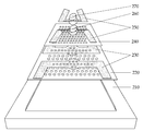
도 2는 본 발명의 제1 실시 예에 따른 1개의 감지 구조체와 1개의 보상 구조체로 구성된 MEMS형 접촉연소식 가스 센서의 개념도,
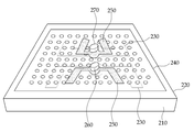
도 3은 도 2에서의 각각 구성 부분들이 합쳐진 1개의 감지 구조체와 1개의 보상 구조체로 구성된 MEMS형 접촉연소식 가스 센서의 도면,
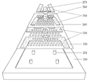
도 4는 본 발명의 제2 실시 예에 따른 1개의 감지 구조체와 1개의 보상 구조체로 구성된 MEMS형 접촉연소식 가스 센서의 또 다른 개념도,
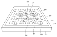
도 5는 도 4에서의 각각 구성 부분들이 합쳐진, 멤브레인을 받쳐주는 기둥이 있는 형태인, MEMS형 접촉연소식 가스 센서의 도면,
도 6 내지 도 12는 본 발명의 실시 예에 따른 MEMS형 접촉연소식 가스 센서내 구조체의 제작 공정에 대한 도면이다.1 is a general circuit diagram of a flammable gas sensing module incorporating a contact combustion gas sensor,
FIG. 2 is a conceptual view of a MEMS type contact combustion gas sensor composed of one sensing structure and one compensation structure according to the first embodiment of the present invention. FIG.
3 is a view of a MEMS type contact combustion gas sensor constituted by one sensing structure and one compensation structure,
4 is another conceptual view of a MEMS type contact combustion gas sensor composed of one sensing structure and one compensation structure according to a second embodiment of the present invention.
5 is a view of a MEMS type contact combustion gas sensor in the form of a column supporting a membrane,
FIGS. 6 to 12 are diagrams showing a manufacturing process of a structure in a MEMS type contact-combustion gas sensor according to an embodiment of the present invention.
하기에서 본 발명을 설명함에 있어 공지 기능 또는 구성에 대한 구체적인 설명이 본 발명의 요지를 불필요하게 흐릴 수 있다고 판단되는 경우에는 그 상세한 설명을 생략한다. 그리고 후술하는 용어들은 본 발명에서의 기능을 고려하여 정의된 용어들로서 이는 사용자 및 운용자의 의도 또는 관례 등에 따라 달라질 수 있다. 그러므로 그 정의는 본 명세서 전반에 걸친 내용을 토대로 내려져야 한다.In the following description, well-known functions or constructions are not described in detail to avoid unnecessarily obscuring the subject matter of the present invention. The following terms are defined in consideration of the functions of the present invention, and these may vary depending on the intention or custom of the user and the operator. Therefore, the definition should be based on the contents throughout this specification.
전술한 바와 같이, 종래 이용되는 접촉연소식 가스 센서는 우수한 감도에도 불구하고 전력 소모가 크거나 구조적으로 충격에 약한 단점이 있어 휴대용 단말기나 USN 서비스용 센서 노드에의 활용이 제한적인 문제점이 있다.As described above, the conventionally used contact-type gas sensor has a drawback in that it consumes a large amount of power and is structurally weak against impact, despite its excellent sensitivity, and thus its application to sensor nodes for portable terminals and USN services is limited.
따라서, 상기와 같은 문제점을 해결하기 위하여, 본 발명은 멤브레인들과 발열 저항체(230) 부분에 다수의 구멍을 뚫고 그 부분들을 통해 기판의 일정 두께만큼 식각하여 열적으로 격리함으로써 전력 소모를 줄이면서도 구조적/기계적으로 안정한 마이크로히터와 이를 이용한 MEMS형 접촉연소식 가스 센서를 제공한다.Accordingly, in order to solve the above-mentioned problems, the present invention provides a semiconductor device having a plurality of holes in a portion of a membrane and a heat generating resistor (230) and thermally isolating the same by etching a predetermined thickness of the substrate through the holes to reduce power consumption, / Mechanically stable micro heater and MEMS type contact combustion gas sensor using the same.
본 발명에서 제공하는 이러한 접촉연소식 가스 센서는 저전력 특성 및 구조적/기계적으로 안정한 특성을 나타내는 이점이 있다.The contact-fired gas sensor provided by the present invention has the advantage of exhibiting low power characteristics and structural / mechanically stable characteristics.
이하, 첨부된 도면을 참조하여 본 발명의 바람직한 실시 예를 상세히 설명한다.Hereinafter, preferred embodiments of the present invention will be described in detail with reference to the accompanying drawings.
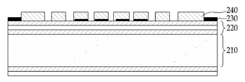
도 2는 본 발명의 제1 실시 예에 따른 1개의 감지 구조체와 1개의 보상 구조체로 구성된 MEMS형 접촉연소식 가스 센서의 개념도이고, 도 3은 도 2에서의 각각 구성 부분들이 합쳐진 1개의 감지 구조체와 1개의 보상 구조체로 구성된 MEMS형 접촉연소식 가스 센서의 도면이다.FIG. 2 is a conceptual view of a MEMS type contact combustion gas sensor composed of one sensing structure and one compensation structure according to the first embodiment of the present invention, and FIG. 3 is a cross- And one compensating structure. In Fig.
도 2에 도시된 바와 같이, 본 발명의 제1 실시 예에 따른 MEMS형 접촉연소식 가스 센서는 1개의 감지 구조체와 1개의 보상 구조체를 포함한다. 도 2에는 감지 구조체와 보상 구조체가 각각 1개로 이루어져 있지만, 1개로 한정되지 않는다. 즉, 본 발명의 제1 실시 예에 따른 MEMS형 접촉연소식 가스 센서는 하나 이상의 감지 구조체와 하나 이상의 보상 구조체를 포함할 수 있다.As shown in FIG. 2, the MEMS type contact gas sensor according to the first embodiment of the present invention includes one sensing structure and one compensation structure. In FIG. 2, the sensing structure and the compensation structure are each formed of one, but the present invention is not limited thereto. That is, the MEMS type contact gas sensor according to the first embodiment of the present invention may include one or more sensing structures and one or more compensation structures.
여기서, 감지 구조체는 다수의 구멍을 가진 제1 멤브레인(220), 제1 멤브레인(220)의 하부에 위치하며 제1 멤브레인(220)의 하부가 노출되도록 중앙 영역이 일정 두께만큼 전체적으로 또는 부분적으로 식각된 기판(210), 제1 멤브레인(220)상의 중앙 영역에 형성되며 접촉연소식 가스센서의 동작에 필요하며, 다수의 구멍을 가진 발열 저항체(230), 발열 저항체(230)를 덮는 형태로 제1 멤브레인(220)과 발열 저항체(230) 위에 형성되고 다수의 구멍을 가진 제2 멤브레인(240), 제2 멤브레인(240)상의 중앙 영역에 형성되고 다수의 구멍을 가진 감지 전극(250) 및 감지 전극(250) 상에 형성된 가스 감지 소재(260)를 포함한다. 하나 이상의 감지 구조체는 경우에 따라서는 감지 전극(250) 부분 중 가스 감지 소재(260)가 위치할 부분을 제외하고 전도성이 없는 소재로 보호층을 포함할 수도 있다.Here, the sensing structure includes a
또한, 보상 구조체는 제1 멤브레인(220), 제1 멤브레인(220)의 하부에 위치하며 제1 멤브레인(220)의 하부가 노출되도록 중앙 영역이 일정 두께만큼 전체적으로 또는 부분적으로 식각된 기판(210), 제1 멤브레인(220)상의 중앙 영역에 형성되며 접촉연소식 가스센서의 동작에 필요하며, 다수의 구멍을 가진 발열 저항체(230), 발열 저항체(230)를 덮는 형태로 제1 멤브레인(220)과 발열 저항체(230) 위에 형성되고 다수의 구멍을 가진 제2 멤브레인(240), 제2 멤브레인(240)상의 중앙 영역에 형성되고 다수의 구멍을 가진 감지 전극(250) 및 감지 전극(250) 상에 형성된 보상 소재(270)를 포함한다.The compensating structure may include a
각 구성요소를 구체적으로 살펴보면, 기판(210)은 일반적인 반도체 공정에서 사용되는 실리콘 기판을 이용할 수 있으며, 산화 알루미늄(Al2O3), 산화 마그네슘(MgO), 석영(quartz), 갈륨-질소(GaN), 갈륨-비소(GaAs) 또는 폴리카보네이트(PC: Polycarbonate), 폴리에틸렌테레프탈레이트(PET: Polyethyleneterephthalate), 폴리에테르술폰(PES: Polyethersulfone), 폴리에틸렌나프탈레이트(PEN: Polyethylene Terephthalate), 폴리이미드(PI: Polyimide) 등의 유연 기판을 이용할 수도 있다. The
제1 멤브레인(220)은 단일 또는 다수의 산화 실리콘 막 또는 질화 실리콘 막으로 구성되고, 열산화 증착법, 스퍼터링 증착법 또는 화학 기상 증착법 등의 방법을 이용하여 형성할 수 있다. 제1 멤브레인(220)은 구조적으로 마이크로히터를 지지하고 기판(210)을 식각할 때에 발열 저항체(230) 부분을 보호하는 역할을 한다. 제1 멤브레인(220)은 다수의 구멍들이 뚫려있고 이 구멍들은 보통 사진 공정과 식각 공정을 통해 패터닝 되며 기판(210)의 식각에 이용된다. The
발열 저항체(230)는 가스 감지 특성 향상을 위하여 주변 온도를 상승시키는 역할을 하며 다수의 구멍들이 뚫려있고 이 구멍들은 보통 사진 공정과 식각 공정을 통해 패터닝 되며 기판(210)의 식각에 이용된다. 발열 저항체(230)는 금(Au), 텅스텐(W), 백금(Pt) 및 팔라듐(Pd) 등의 금속 또는 실리콘 또는 전도성 금속 산화물 등을 이용하여 형성할 수 있다. 발열 저항체(230)는 기판(210) 중앙 영역의 멤브레인 상에 형성되며, 스퍼터링 증착법(sputtering), 전자빔 증착법(e-beam) 또는 기화 증착법(evaporation) 등의 방법을 이용하여 형성될 수 있다.The heat generating
한편, 발열 저항체(230) 형성시에 접착력을 더 높이기 위하여 멤브레인 상에 크롬(Cr) 또는 티타늄(Ti) 등을 이용한 부착층(미도시)을 더 형성할 수 있다. 상기 부착층은 스퍼터링 증착법, 전자빔 증착법 또는 기화 증착법 등의 방법을 이용하여 형성될 수 있다. 발열 저항체(230)는 히터 전극 패드 및 본딩 와이어에 의하여 외부 회로(미도시)와 연결될 수 있다.On the other hand, an adhesion layer (not shown) using chromium (Cr), titanium (Ti) or the like may be further formed on the membrane in order to further increase the adhesive force when the
제2 멤브레인(240)은 단일 또는 다수의 산화 실리콘 막 또는 질화 실리콘 막으로 구성되고 열산화 증착법, 스퍼터링 증착법 또는 화학 기상 증착법 등의 방법을 이용하여 형성할 수 있다. 제2 멤브레인(240)은 발열 저항체(230)와 감지 전극(250) 사이에 위치하며 두 전극을 전기적으로 절연하고 마이크로히터를 구조적으로 지지하는 역할을 하며, 다수의 구멍들이 뚫려있고 이 구멍들은 보통 사진 공정과 식각 공정을 통해 패터닝 되며 기판(210)의 식각에 이용된다.The
감지 전극(250)은 가스 감지 소재(260)에서의 가스 흡착 및 탈착에 따른 저항값 변화를 외부로 출력한다. 감지 전극(250)은 기판(210) 중앙 영역의 제1 멤브레인(220) 위에 형성되며, 바람직하게는 기판(210)의 중앙 영역을 지나도록 한 쌍이 형성된다. 감지 전극(250)은 인터디지털(inter-digital) 형태 또는 갭(gap) 형태로 형성되고, 백금(Pt), 알루미늄(Al), 금(Au) 같은 금속 또는 전도성 금속 산화물 등을 이용하여 스퍼터링 증착법, 전자빔 증착법 또는 기화 증착법 등의 방법에 의하여 형성할 수 있다. 감지 전극(250)의 양단에는 신호 전달을 위한 본딩 와이어(미도시)가 접촉된다. The
경우에 따라서는 감지 전극(250) 상부 중에서 가스 감지 소재(260)가 위치할 부분을 제외하고 전도성이 없는 소재로 보호층이 포함될 수도 있으며, 실리콘 막 또는 질화 실리콘 막 등으로 형성하며, 열산화 증착법, 스퍼터링 증착법 또는 화학 기상 증착법 등의 방법을 이용하여 형성할 수 있다.In some cases, the protective layer may be formed of a material having no conductivity except for the portion where the
가스 감지 소재(260)는 가스를 흡착하여 연소열에 의한 온도변화에 따른 저항 변화를 보기 위한 가스 감지 소재(260)로서, 금속 산화물, 탄소 나노 튜브(Carbon Nano Tube; CNT) 및 그라핀(graphene) 등의 물질에 귀금속인 백금이나 팔라듐 등의 귀금속을 첨가하여 제작한다. 보상 소재(270)에는 촉매 역할을 하는 귀금속을 첨가하지 않고 이용하며, 솔-젤법, 전기 방사법, 잉크젯 프린팅법, 스크린 프린팅법, 스퍼터링 증착법 또는 화학 기상 증착법 등의 방법을 이용하여 형성할 수 있다.The
상기와 같은 구성을 갖는 본 발명의 제1 실시 예에 따른 MEMS형 접촉연소식 가스 센서는, 소모 전력을 최소화하면서도 갑작스런 충격이나 오랜 구동에서도 멤브레인의 변형을 최소화하여 수명을 늘리고 다양한 환경에서 작동할 수 있는 이점이 있다.The MEMS type contact combustion type gas sensor according to the first embodiment of the present invention having the above-described structure can minimize the deformation of the membrane even when sudden shock or long driving, while minimizing power consumption, There is an advantage.
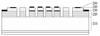
도 4는 본 발명의 제2 실시 예에 따른 1개의 감지 구조체와 1개의 보상 구조체로 구성된 MEMS형 접촉연소식 가스 센서의 또 다른 개념도이고, 도 5는 도 4에서의 각각 구성 부분들이 합쳐진, 멤브레인을 받쳐주는 기둥이 있는 형태인, MEMS형 접촉연소식 가스 센서의 도면이다.4 is another conceptual view of a MEMS type contact-combustion gas sensor composed of one sensing structure and one compensation structure according to a second embodiment of the present invention, and Fig. 5 is a cross- In the form of a column supporting the MEMS type contact combustion gas sensor.
전술된 본 발명의 제1 실시 예에 따른 도 2와 다른 구성은 다수의 구멍을 적절히 배치하여 멤브레인들과 발열 저항체(230) 아래의 기판(210) 부분을 식각할 때, 기판(210)의 일부분을 남겨서 멤브레인들을 떠받치는 기둥(211)을 형성하도록 하는 점이다. 이와 같이, 일부분이 식각되어 기둥(211)이 형성된 기판(210)은 갑작스런 충격이나 반복되는 동작하에서도 멤브레인들의 변형을 최소화하여 센서의 수명을 늘리도록 한다.2, in accordance with the first embodiment of the present invention described above, when a plurality of holes are appropriately arranged to etch the portions of the
도 6 내지 도 12는 본 발명의 실시 예에 따른 MEMS형 접촉연소식 가스 센서내 구조체의 제작 공정에 대한 도면이다.Figs. 6 to 12 are diagrams showing a manufacturing process of a structure in a MEMS type contact-combustion gas sensor according to an embodiment of the present invention.
도 6에 도시된 바와 같이, 단면 폴리싱된 실리콘 기판(210)에 제1 멤브레인(220)용으로 단일 층 또는 다층의 산화 실리콘 막 또는 질화 실리콘 막이 열산화 증착법, 스퍼터링 증착법 또는 화학 기상 증착법 등의 방법을 이용하여 증착된다.6, a single-layer or multi-layer silicon oxide film or silicon nitride film for the
도 7에 도시된 바와 같이, 그 위에 발열 저항체(230)용으로 금(Au), 텅스텐(W), 백금(Pt) 및 팔라듐(Pd) 등의 금속 막 또는 실리콘 막 또는 전도성 금속 산화물 막 등을 스퍼터링 증착법, 전자빔 증착법 또는 기화 증착법 등의 방법을 이용하여 증착하고 설계된 대로 사진 공정을 통해 패터닝한다.A metal film such as gold (Au), tungsten (W), platinum (Pt) and palladium (Pd), a silicon film or a conductive metal oxide film or the like is formed thereon for the
도 8에 도시된 바와 같이, 그 다음 제2 멤브레인(240)용으로 단일 층 또는 다층의 산화 실리콘 막 또는 질화 실리콘 막이 열산화 증착법, 스퍼터링 증착법 또는 화학 기상 증착법 등의 방법을 이용하여 증착되고 설계된 대로 사진 공정을 통해 패터닝한다.As shown in FIG. 8, a single layer or multilayer silicon oxide film or silicon nitride film is then deposited and designed for the
도 9에 도시된 바와 같이, 그 위에 감지 전극(250)용으로 백금(Pt), 알루미늄(Al) 또는 금(Au) 등의 금속막 또는 전도성 금속 산화물 등을 스퍼터링 증착법, 전자빔 증착법 또는 기화 증착법 등의 방법에 의하여 증착하고 설계된 대로 사진 공정을 통해 패터닝한다.A metal film or a conductive metal oxide such as platinum (Pt), aluminum (Al), or gold (Au) is deposited on the
도 10에 도시된 바와 같이, 멤브레인들과 발열 저항체(230) 부분들을 열적으로 격리하기 위하여 그 밑으로 기판(210)의 일정 두께 부분을 식각하는데 그 전에 식각할 영역에 대해 사진 공정과 식각 공정을 통해 패터닝한다.As shown in FIG. 10, a certain thickness portion of the
도 11에 도시된 바와 같이, 기판 식각 공정은 구멍으로 드러나지 않는 기판(210) 부분에 대해서도 식각해야 하는 등방 식각 공정이 위주이고 XeF2 가스를 이용한 방법이 주로 사용된다.As shown in FIG. 11, the substrate etching process mainly uses an isotropic etching process for etching the portion of the
한편, 도 12에 도시된 바와 같이, 기판(210)을 식각할 때, 기판(210)의 일부분을 남겨서 멤브레인들(220, 240)을 지지하는 기둥(211)을 형성한다.12, when the
가스 감지 소재(260)의 증착 방법에 따라 가스 감지 소재 증착 공정과 기판(210) 식각 공정의 순서가 달라진다. 예를 들어, 스크린 프린팅법 같이 기판(210)에 압력이 가해지는 감지 소재 증착법을 적용하는 경우에는 가스 감지 소재(260)를 먼저 증착하고 일정 두께의 실리콘을 식각하여 MEMS형 접촉연소식 가스 센서를 제작하고, 솔-젤법이나 전기 방사법, 잉크젯 프린팅법, 스퍼터링 증착법 그리고 화학적 기상 증착법 같이 기판(210)에 압력이 가해지지 않는 감지 소재 증착법을 적용하는 경우에는 일정 두께의 실리콘을 먼저 식각하고 가스 감지 소재(260)를 나중에 증착할 수도 있다.The order of the gas sensing material deposition process and the
또한, 경우에 따라서는 도 6 내지 도 12에는 나와있지 않지만 가스 감지용 전극을 보호하기 위하여 SiO2나 SiNx 등의 절연막을 증착하고 패터닝하는 공정을 추가할 수도 있다.In some cases, although not shown in FIGS. 6 to 12, a process of depositing and patterning an insulating film such as SiO 2 or SiNx may be added to protect the gas sensing electrode.
이상의 설명은 본 발명을 예시적으로 설명한 것에 불과하며, 본 발명이 속하는 기술 분야에서 통상의 지식을 가진 자에 의해 본 발명의 기술적 사상에서 벗어나지 않는 범위에서 다양한 변형이 가능할 것이다. 따라서 본 발명의 명세서에 개시된 실시 예들은 본 발명을 한정하는 것이 아니다. 본 발명의 범위는 아래의 특허청구범위에 의해 해석되어야 하며, 그와 균등한 범위 내에 있는 모든 기술도 본 발명의 범위에 포함되는 것으로 해석해야 할 것이다.The foregoing description is merely illustrative of the present invention, and various modifications may be made by those skilled in the art without departing from the spirit of the present invention. Accordingly, the embodiments disclosed in the specification of the present invention are not intended to limit the present invention. The scope of the present invention should be construed according to the following claims, and all the techniques within the scope of equivalents should be construed as being included in the scope of the present invention.
본 발명은 초소형이면서 소모 전력이 현저히 줄어든 MEMS형 접촉연소식 가스 센서에서 구조적/기계적/전기적으로 안정하며 소자 제작 공정이 용이한 가스 센서를 제공할 수 있다. 이러한 점에서 기존 기술의 한계를 뛰어 넘음에 따라 관련 기술에 대한 이용만이 아닌 적용되는 장치의 시판 또는 영업의 가능성이 충분할 뿐만 아니라 현실적으로 명백하게 실시할 수 있는 정도이므로 산업상 이용 가능성이 있는 발명이다.The present invention can provide a gas sensor which is structurally / mechanically / electrically stable and which is easy to manufacture in a MEMS type contact combustion gas sensor which is very small and consumes significantly less power. In this respect, it is not only the use of the related technology but also the possibility of commercialization or operation of the applied device, as it exceeds the limit of the existing technology.
210: 기판 220: 제1 멤브레인
230: 발열 저항체 240: 제2 멤브레인
250: 감지 전극 260: 가스 감지 소재
270: 보상 소재 211: 기둥210: substrate 220: first membrane
230: heat generating resistor 240: second membrane
250: sensing electrode 260: gas sensing material
270: Compensation material 211: Column
Claims (8)
상기 제1 멤브레인의 하부에 위치하되 하부면의 일부분과는 비접촉되도록 중앙 영역이 일정 두께만큼 식각된 기판;
상기 제1 멤브레인의 상면 중앙 영역에 형성되고 다수의 구멍을 가진 발열 저항체;
상기 제1 멤브레인과 상기 발열 저항체 위에 형성되고 다수의 구멍을 가진 제2 멤브레인;
상기 제2 멤브레인상의 중앙 영역에 형성되고 다수의 구멍을 가진 감지 전극;
상기 감지 전극 상에 가스 감지 소재로 형성된 하나 이상의 감지 구조체; 및
상기 감지 전극 상에 보상 소재로 형성된 하나 이상의 보상 구조체
를 포함하는 것을 특징으로 하는 접촉연소식 가스 센서.A first membrane having a plurality of apertures;
A substrate disposed at a lower portion of the first membrane and having a central region etched by a predetermined thickness so as to be in non-contact with a portion of the lower surface;
A heat generating resistor formed in the central region of the upper surface of the first membrane and having a plurality of holes;
A second membrane formed on the first membrane and the heat generating resistor and having a plurality of holes;
A sensing electrode formed in a central region on the second membrane and having a plurality of holes;
At least one sensing structure formed of a gas sensing material on the sensing electrode; And
Wherein at least one compensation structure formed of a compensation material on the sensing electrode
Wherein the gas sensor is a gas sensor.
상기 제1 멤브레인 하부의 기판은,
상기 제2 멤브레인 및 상기 제1 멤브레인과 상기 발열 저항체에 있는 다수의 구멍을 통해 전체적으로 식각되어 상기 제1 멤브레인을 지탱하는 기둥이 없는 구조인 것을 특징으로 하는 접촉연소식 가스 센서.The method according to claim 1,
Wherein the substrate under the first membrane comprises:
Wherein the second contact is a structure that is entirely etched through the plurality of holes in the second membrane, the first membrane, and the heat generating resistor so as to have no column supporting the first membrane.
상기 제1 멤브레인 하부의 기판은,
상기 제2 멤브레인 및 상기 제1 멤브레인과 상기 발열 저항체에 있는 다수의 구멍을 통해 부분적으로 식각되어 상기 제1 멤브레인을 지탱하는 기둥이 있는 구조인 것을 특징으로 하는 접촉연소식 가스 센서.The method according to claim 1,
Wherein the substrate under the first membrane comprises:
Wherein the structure is a structure in which the second membrane and the first membrane are partially etched through a plurality of holes in the heat generating resistor and a column supporting the first membrane.
상기 제2 멤브레인과 상기 제1 멤브레인은,
단일 층 또는 다층의 산화 실리콘 막 또는 질화 실리콘 막이 열산화 증착법, 스퍼터링 증착법 및 화학 기상 증착법 중 어느 하나의 방법을 이용하여 증착된 것을 특징으로 하는 접촉연소식 가스 센서. The method according to claim 1,
The second membrane and the first membrane may be formed,
Wherein a single layer or a multi-layer silicon oxide film or a silicon nitride film is deposited by any one of a thermal oxidation deposition method, a sputter deposition method, and a chemical vapor deposition method.
상기 발열 저항체는,
금(Au), 텅스텐(W), 백금(Pt) 및 팔라듐(Pd) 중 어느 하나의 금속막 또는 실리콘 막 또는 전도성 금속 산화물 막을 스퍼터링 증착법, 전자빔 증착법 및 기화 증착법 중 어느 하나의 방법을 이용하여 증착된 것을 특징으로 하는 접촉연소식 가스 센서.The method according to claim 1,
The heat generating resistor
A metal film or a silicon film or a conductive metal oxide film of any one of gold (Au), tungsten (W), platinum (Pt) and palladium (Pd) is deposited by any one of a sputtering deposition method, an electron beam vapor deposition method and a vapor deposition method Wherein the gas sensor is a gas sensor.
상기 감지 전극은,
백금(Pt), 알루미늄(Al) 및 금(Au) 중 어느 하나의 금속 막 또는 전도성 금속 산화물 막을 스퍼터링 증착법, 전자빔 증착법 및 기화 증착법 중 어느 하나의 방법에 의하여 증착된 것을 특징으로 하는 접촉연소식 가스 센서.The method according to claim 1,
The sensing electrode
Characterized in that a metal film or a conductive metal oxide film of any one of platinum (Pt), aluminum (Al) and gold (Au) is deposited by any one of a sputtering deposition method, an electron beam deposition method and a vapor deposition method sensor.
상기 가스 감지 소재는, 금속 산화물, 탄소 나노 튜브(Carbon Nano Tube; CNT) 및 그라핀(graphene) 중 어느 하나의 물질에 귀금속인 백금이나 팔라듐 등의 귀금속을 첨가하여 이루어지고,
상기 보상 소재는, 촉매 역할을 하는 귀금속을 첨가하지 않고 이용할 수 있으며, 솔-젤법, 드롭 코팅법, 스크린 프린팅법, 화학 기상 증착법 및 스퍼터링 증착법 중 어느 하나의 방법을 이용하여 증착된 것을 특징으로 하는 접촉연소식 가스 센서.The method according to claim 1,
The gas sensing material is formed by adding a noble metal such as platinum or palladium, which is a noble metal, to any one of a metal oxide, a carbon nanotube (CNT) and a graphene,
The compensation material can be used without adding a noble metal serving as a catalyst, and is deposited using any one of a sol-gel method, a drop coating method, a screen printing method, a chemical vapor deposition method, and a sputtering deposition method Contact combustion gas sensor.
상기 기판은,
실리콘, 산화 알루미늄(Al2O3), 산화 마그네슘(MgO), 석영(quartz), 갈륨-질소(GaN), 갈륨-비소(GaAs) 또는 폴리카보네이트(PC), 폴리에틸렌테레프탈레이트(PET), 폴리에테르술폰(PES), 폴리에틸렌나프탈레이트(PEN), 폴리이미드(PI) 중 어느 하나를 이용하여 제작된 것을 특징으로 하는 접촉연소식 가스 센서.The method according to claim 1,
Wherein:
(Al 2 O 3 ), magnesium oxide (MgO), quartz, gallium-nitrogen (GaN), gallium-arsenic (GaAs) or polycarbonate (PC), polyethylene terephthalate (PES), polyethylene naphthalate (PEN), and polyimide (PI).
Priority Applications (2)
| Application Number | Priority Date | Filing Date | Title |
|---|---|---|---|
| KR1020130009883A KR20140097714A (en) | 2013-01-29 | 2013-01-29 | Mems catalytic type gas sensor using multi-holes membrane embedded micro-heater |
| US13/897,293 US20140208838A1 (en) | 2013-01-29 | 2013-05-17 | Micro electro mechanical system catalytic combustible gas sensor using porous membrane embedded micro-heater |
Applications Claiming Priority (1)
| Application Number | Priority Date | Filing Date | Title |
|---|---|---|---|
| KR1020130009883A KR20140097714A (en) | 2013-01-29 | 2013-01-29 | Mems catalytic type gas sensor using multi-holes membrane embedded micro-heater |
Publications (1)
| Publication Number | Publication Date |
|---|---|
| KR20140097714A true KR20140097714A (en) | 2014-08-07 |
Family
ID=51221472
Family Applications (1)
| Application Number | Title | Priority Date | Filing Date |
|---|---|---|---|
| KR1020130009883A KR20140097714A (en) | 2013-01-29 | 2013-01-29 | Mems catalytic type gas sensor using multi-holes membrane embedded micro-heater |
Country Status (2)
| Country | Link |
|---|---|
| US (1) | US20140208838A1 (en) |
| KR (1) | KR20140097714A (en) |
Families Citing this family (8)
| Publication number | Priority date | Publication date | Assignee | Title |
|---|---|---|---|---|
| DE102014000343A1 (en) * | 2014-01-11 | 2015-07-16 | Dräger Safety AG & Co. KGaA | gas meter |
| WO2016025727A2 (en) * | 2014-08-13 | 2016-02-18 | Vorbeck Materials Corp. | Surface applied sensors |
| US9658179B2 (en) * | 2015-06-24 | 2017-05-23 | Infineon Technologies Ag | System and method for a MEMS transducer |
| US10524510B2 (en) | 2017-07-07 | 2020-01-07 | Funai Electric Co., Ltd. | Heater for a vaporization device |
| CN108732212B (en) * | 2018-05-23 | 2020-12-15 | 哈尔滨工程大学 | Manufacturing method of multi-effect detection integrated gas sensor, sensor and application of sensor |
| US10900922B2 (en) * | 2018-07-17 | 2021-01-26 | Msa Technology, Llc | Power reduction in combustible gas sensors |
| CN110361423B (en) * | 2019-07-12 | 2023-04-07 | 北京机械设备研究所 | MEMS gas sensor and method for improving stability of MEMS gas sensor |
| US11114223B1 (en) * | 2020-07-27 | 2021-09-07 | Tronics MEMS, Inc. | Three-dimensional thermistor platform and a method for manufacturing the same |
Family Cites Families (7)
| Publication number | Priority date | Publication date | Assignee | Title |
|---|---|---|---|---|
| WO2000032512A1 (en) * | 1998-12-02 | 2000-06-08 | Massachusetts Institute Of Technology | Integrated palladium-based micromembranes for hydrogen separation and hydrogenation/dehydrogenation reactions |
| US6888467B2 (en) * | 2002-12-10 | 2005-05-03 | Industrial Scientific Corporation | Gas detection instrument and method for its operation |
| JP2006153598A (en) * | 2004-11-26 | 2006-06-15 | Honda Motor Co Ltd | Gas detector and control method of gas detecting element |
| DE102005050914B4 (en) * | 2005-10-21 | 2009-04-16 | Dräger Safety AG & Co. KGaA | Portable gas meter |
| DE112008000824T5 (en) * | 2007-03-28 | 2010-02-11 | HORIBA, Ltd., Kyoto-shi | Sensor for flammable gases |
| US8683847B2 (en) * | 2011-02-09 | 2014-04-01 | Electronics And Telecommunications Research Institute | Microelectromechanical systems type semiconductor gas sensor using microheater having many holes and method for manufacturing the same |
| EP2559996B1 (en) * | 2011-08-16 | 2017-11-22 | Nxp B.V. | Gas sensor |
-
2013
- 2013-01-29 KR KR1020130009883A patent/KR20140097714A/en not_active Application Discontinuation
- 2013-05-17 US US13/897,293 patent/US20140208838A1/en not_active Abandoned
Also Published As
| Publication number | Publication date |
|---|---|
| US20140208838A1 (en) | 2014-07-31 |
Similar Documents
| Publication | Publication Date | Title |
|---|---|---|
| KR20140097714A (en) | Mems catalytic type gas sensor using multi-holes membrane embedded micro-heater | |
| KR101772575B1 (en) | Micro Semiconducting Gas Sensors for Low power operation and its fabrication method | |
| US8683847B2 (en) | Microelectromechanical systems type semiconductor gas sensor using microheater having many holes and method for manufacturing the same | |
| KR101094870B1 (en) | humidity sensor and manufacturing method thereof | |
| KR101773954B1 (en) | Micro Electro Mechanical Systems Type Electrochemical Gas Sensor | |
| US9134276B2 (en) | Bulk acoustic wave resonator sensor | |
| US10697920B2 (en) | Gas sensor | |
| KR20090064693A (en) | Micro gas sensor and manufacturing method thereof | |
| JP5862046B2 (en) | Hydrogen gas sensor | |
| US20170363556A1 (en) | Gas sensor | |
| JP4994058B2 (en) | Pressure measuring device and pressure measuring method | |
| KR101519033B1 (en) | Micro Electro Mechanical Systems Type Semiconductor Gas Sensor Using Microheater Having Many Holes and Method for Manufacturing the Same | |
| KR20110066849A (en) | Semiconductor gas sensor with low power consumption | |
| KR100906496B1 (en) | Gas sensor and method for manufacturing the same | |
| KR100537093B1 (en) | Carbon nanotubes based gas sensor on mems structure and method for fabricating thereof | |
| KR20200097068A (en) | Gas sensing device and method thereof | |
| JP6372686B2 (en) | Gas detection device and gas detection method | |
| JP3137252U (en) | Pressure sensor for sealed container and sealed container | |
| JP4798961B2 (en) | HEATER DEVICE AND GAS SENSOR DEVICE USING THE SAME | |
| US20220128498A1 (en) | Gas sensor and manufacturing method thereof | |
| KR20050081691A (en) | Method for manufacturing micro-structure catalytic combustion type gas sensor, and gas sensor using the micro-structure catalytic combustion gas sensor | |
| JP2013174627A (en) | Gas sensor | |
| JP2012189537A (en) | Gas sensor | |
| JP7421442B2 (en) | MEMS type semiconductor gas detection element | |
| JP7421441B2 (en) | MEMS type semiconductor gas detection element |
Legal Events
| Date | Code | Title | Description |
|---|---|---|---|
| WITN | Application deemed withdrawn, e.g. because no request for examination was filed or no examination fee was paid |