KR20140078455A - Touch panel and method of fabricating the same - Google Patents
Touch panel and method of fabricating the same Download PDFInfo
- Publication number
- KR20140078455A KR20140078455A KR1020120147829A KR20120147829A KR20140078455A KR 20140078455 A KR20140078455 A KR 20140078455A KR 1020120147829 A KR1020120147829 A KR 1020120147829A KR 20120147829 A KR20120147829 A KR 20120147829A KR 20140078455 A KR20140078455 A KR 20140078455A
- Authority
- KR
- South Korea
- Prior art keywords
- transparent electrode
- coating layer
- substrate
- touch panel
- transparent
- Prior art date
Links
Images


Classifications
-
- G—PHYSICS
- G06—COMPUTING; CALCULATING OR COUNTING
- G06F—ELECTRIC DIGITAL DATA PROCESSING
- G06F3/00—Input arrangements for transferring data to be processed into a form capable of being handled by the computer; Output arrangements for transferring data from processing unit to output unit, e.g. interface arrangements
- G06F3/01—Input arrangements or combined input and output arrangements for interaction between user and computer
- G06F3/03—Arrangements for converting the position or the displacement of a member into a coded form
- G06F3/041—Digitisers, e.g. for touch screens or touch pads, characterised by the transducing means
- G06F3/044—Digitisers, e.g. for touch screens or touch pads, characterised by the transducing means by capacitive means
-
- G—PHYSICS
- G06—COMPUTING; CALCULATING OR COUNTING
- G06F—ELECTRIC DIGITAL DATA PROCESSING
- G06F3/00—Input arrangements for transferring data to be processed into a form capable of being handled by the computer; Output arrangements for transferring data from processing unit to output unit, e.g. interface arrangements
- G06F3/01—Input arrangements or combined input and output arrangements for interaction between user and computer
- G06F3/03—Arrangements for converting the position or the displacement of a member into a coded form
- G06F3/041—Digitisers, e.g. for touch screens or touch pads, characterised by the transducing means
- G06F3/045—Digitisers, e.g. for touch screens or touch pads, characterised by the transducing means using resistive elements, e.g. a single continuous surface or two parallel surfaces put in contact
-
- G—PHYSICS
- G06—COMPUTING; CALCULATING OR COUNTING
- G06F—ELECTRIC DIGITAL DATA PROCESSING
- G06F2203/00—Indexing scheme relating to G06F3/00 - G06F3/048
- G06F2203/041—Indexing scheme relating to G06F3/041 - G06F3/045
- G06F2203/04103—Manufacturing, i.e. details related to manufacturing processes specially suited for touch sensitive devices
Abstract
Description
실시예는 터치 패널 및 이의 제조방법에 관한 것이다.Embodiments relate to a touch panel and a method of manufacturing the touch panel.
최근 다양한 전자 제품에서 디스플레이 장치에 표시된 화상에 손가락 또는 스타일러스(stylus) 등의 입력 장치를 접촉하는 방식으로 입력을 하는 터치 패널이 적용되고 있다.2. Description of the Related Art In recent years, a touch panel has been applied to an image displayed on a display device in various electronic products by a method of touching an input device such as a finger or a stylus.
터치 패널은 크게 저항막 방식의 터치 패널과 정전 용량 방식의 터치 패널로 구분될 수 있다. 저항막 방식의 터치 패널은 입력 장치의 압력에 의하여 유리와 전극이 단락되어 위치가 검출된다. 정전 용량 방식의 터치 패널은 손가락이 접촉했을 때 전극 사이의 정전 용량이 변화하는 것을 감지하여 위치가 검출된다.The touch panel can be largely divided into a resistance film type touch panel and a capacitive type touch panel. In the resistive touch panel, the glass and the electrode are short-circuited by the pressure of the input device and the position is detected. A capacitance type touch panel senses a change in electrostatic capacitance between electrodes when a finger touches them, thereby detecting the position.
이러한 터치 패널의 투명전극으로써, 인듐 주석 산화물(indium tin oxide, ITO)을 대체할 수 있는 물질인 나노와이어가 대두되고 있다. 나노와이어는 투과도 및 전도도 등 다양한 면에서 인듐 주석 산화물보다 뛰어난 특성을 가진 물질이다.Nanowires, which can replace indium tin oxide (ITO), are emerging as transparent electrodes of such touch panels. Nanowires are superior to indium tin oxide in various aspects such as transmittance and conductivity.
이러한 투명 전극은 기판 상에 형성되게 되는데, 상기 투명 전극에 대해 패터닝 고정을 수행할 때, 상기 투명 전극과 상기 기판의 낮은 밀착력으로 인해, 상기 투명 전극이 상기 기판으로부터 떨어져 나가는 문제점이 있다.The transparent electrode is formed on the substrate. When patterning and fixing the transparent electrode, the transparent electrode is separated from the substrate due to a low adhesion between the transparent electrode and the substrate.
이에 따라, 상기 기판과 상기 투명 전극의 밀착력을 향상시킬 수 있는 터치 패널 및 이의 제조방법의 필요성이 요구된다.Accordingly, there is a need for a touch panel capable of improving adhesion between the substrate and the transparent electrode and a method for manufacturing the touch panel.
실시예는 신뢰성이 향상된 터치 패널 및 이의 제조방법을 제공하고자 한다.Embodiments provide a touch panel with improved reliability and a manufacturing method thereof.
실시예에 따른 터치 패널은, 기판; 상기 기판 상에 형성되는 투명 전극; 및 상기 기판 상에 형성되고, 상기 투명 전극의 측면과 직접 접촉하는 코팅층을 포함한다.A touch panel according to an embodiment includes a substrate; A transparent electrode formed on the substrate; And a coating layer formed on the substrate and in direct contact with a side surface of the transparent electrode.
실시예에 따른 터치 패널 제조방법은, 기판을 준비하는 단계; 상기 기판 상에 투명 전극 물질을 도포하여 투명 전극을 형성하는 단계; 상기 기판 상에 제 1 코팅층 물질을 도포하여 제 1 코팅층을 형성하는 단계; 및 상기 투명 전극을 패터닝하여 다수 개의 투명 전극들을 형성하는 단계를 포함하고, 상기 제 1 코팅층은 상기 투명 전극의 측면과 직접 접촉하며 형성된다.A method of manufacturing a touch panel according to an embodiment includes preparing a substrate; Forming a transparent electrode by applying a transparent electrode material on the substrate; Forming a first coating layer by applying a first coating material on the substrate; And forming a plurality of transparent electrodes by patterning the transparent electrode, wherein the first coating layer is formed in direct contact with a side surface of the transparent electrode.
실시예에 따른 터치 패널은 상기 제 1 코팅층에 의해 상기 기판과 상기 투명 전극의 밀착력을 향상시킬 수 있다. 따라서, 실시예에 따른 터치 패널은 상기 투명 전극을 패터닝하여도, 향상된 밀착력으로 인해, 상기 투명 전극이 상기 기판으로부터 이탈하는 것을 방지할 수 있고, 또한, 상기 제 1 코팅층이 상기 투명 전극의 측면과 직접 접촉하여 형성되므로, 상기 투명 전극의 산화를 방지할 수 있으므로, 터치 패널의 신뢰도를 향상시킬 수 있다.The touch panel according to the embodiment can improve adhesion between the substrate and the transparent electrode by the first coating layer. Therefore, even when the transparent electrode is patterned, the touch panel according to the embodiment can prevent the transparent electrode from being detached from the substrate due to the enhanced adhesion, and the first coating layer can prevent the transparent electrode from being separated from the side surface of the transparent electrode The transparent electrode can be prevented from being oxidized, so that the reliability of the touch panel can be improved.
실시예에 따른 터치 패널 제조방법은, 상기 투명 전극을 패터닝하기 전에 상기 투명 전극 상에 제 1 코팅층을 형성한다. 즉, 상기 투명 전극 물질을 상기 기판 상에 도포한 후, 상기 투명 전극 물질 상에 상기 제 1 코팅층 형성 물질인 고분자 절연 수지를 도포한다.A method of manufacturing a touch panel according to an embodiment of the present invention includes forming a first coating layer on the transparent electrode before patterning the transparent electrode. That is, the transparent electrode material is coated on the substrate, and then the polymer insulating resin as the first coating layer forming material is coated on the transparent electrode material.
이에 따라, 상기 투명 전극 상에 도포되어 형성되는 상기 제 1 코팅층은 상기 기판과 상기 투명 전극의 밀착력을 강화함으로써, 이후에 형성되는 투명 전극의 패터닝 공정시 상기 투명 전극이 상기 기판에서 이탈되는 것을 방지할 수 있다.Accordingly, the first coating layer formed on the transparent electrode enhances adhesion between the substrate and the transparent electrode, thereby preventing the transparent electrode from being detached from the substrate during the patterning process of the transparent electrode to be formed later can do.
또한, 상기 패터닝 공정 후에도, 상기 제 2 코팅층은 상기 투명 전극들 사이에 배치됨으로써, 상기 기판과 상기 투명 전극의 밀착력을 향상시킴과 동시에, 상기 투명 전극들이 외부에 노출되었을 때, 투명 전극이 산화되는 것을 방지할 수 있다.Also, after the patterning process, the second coating layer is disposed between the transparent electrodes to improve adhesion between the substrate and the transparent electrodes, and when the transparent electrodes are exposed to the outside, the transparent electrodes are oxidized Can be prevented.
따라서, 실시예에 따른 터치 패널 제조방법은, 투명 전극을 기판 상에 형성한 후, 패터닝 공정을 진행하기 전에, 밀착력 강화 및 산화 방지 역할을 하는 제 1 코팅층을 형성함으로써, 투명 전극의 손상을 방지하고, 터치 패널의 신뢰도를 향상시킬 수 있다.Therefore, in the method of manufacturing a touch panel according to the embodiment, after forming the transparent electrode on the substrate, the first coating layer serving to strengthen the adhesion and prevent oxidation is formed before the patterning process, And the reliability of the touch panel can be improved.
도 1은 실시예에 따른 터치 패널의 단면도를 도시한 도면이다.
도 2는 다른 실시예에 따른 터치 패널의 단면도를 도시한 도면이다.
도 3은 실시예에 따른 터치 패널의 일 평면도이다.
도 4는 실시예에 따른 터치 패널 제조방법을 설명하기 위한 공정 흐름도이다.
도 5 내지 도 9는 실시예에 따른 터치 패널 제조방법을 설명하기 위한 도면들이다.1 is a cross-sectional view of a touch panel according to an embodiment.
2 is a cross-sectional view of a touch panel according to another embodiment.
3 is a plan view of the touch panel according to the embodiment.
4 is a flowchart illustrating a method of manufacturing a touch panel according to an embodiment of the present invention.
5 to 9 are views for explaining a method of manufacturing a touch panel according to an embodiment.
실시예들의 설명에 있어서, 각 층(막), 영역, 패턴 또는 구조물들이 기판, 각 층(막), 영역, 패드 또는 패턴들의 “상/위(on)”에 또는 “하/아래(under)”에 형성된다는 기재는, 직접(directly) 또는 다른 층을 개재하여 형성되는 것을 모두 포함한다. 각 층의 상/위 또는 하/아래에 대한 기준은 도면을 기준으로 설명한다. In the description of the embodiments, it is to be understood that each layer (film), area, pattern or structure may be referred to as being "on" or "under / under" Quot; includes all that is formed directly or through another layer. The criteria for top / bottom or bottom / bottom of each layer are described with reference to the drawings.
도면에서 각 층(막), 영역, 패턴 또는 구조물들의 두께나 크기는 설명의 명확성 및 편의를 위하여 변형될 수 있으므로, 실제 크기를 전적으로 반영하는 것은 아니다. The thickness or the size of each layer (film), region, pattern or structure in the drawings may be modified for clarity and convenience of explanation, and thus does not entirely reflect the actual size.
이하, 첨부한 도면을 참조하여 본 발명의 실시예를 상세하게 설명하면 다음과 같다.
Hereinafter, embodiments of the present invention will be described in detail with reference to the accompanying drawings.
이하, 도 1 내지 도 3을 참조하여, 실시예에 따른 터치 패널을 상세하게 설명한다. 도 1은 실시예에 따른 터치 패널의 단면도를 도시한 도면이고, 도 2는 다른 실시예에 따른 터치 패널의 단면도를 도시한 도면이며, 도 3은 실시예에 따른 터치 패널의 일 평면도이다.Hereinafter, a touch panel according to an embodiment will be described in detail with reference to FIGS. 1 to 3. FIG. FIG. 1 is a sectional view of a touch panel according to an embodiment of the present invention. FIG. 2 is a sectional view of a touch panel according to another embodiment. FIG. 3 is a plan view of a touch panel according to an embodiment.
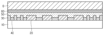
도 1 내지 도 3을 참조하면, 실시예에 따른 터치 패널은, 기판(10), 투명 전극(20), 배선 전극(30), 제 1 코팅층(40), 제 2 코팅층(50), 접착층(60)을 포함한다.1 to 3, a touch panel according to an embodiment includes a
상기 기판(10은 상기 기판(10) 상에 형성되는 상기 투명 전극(20), 상기 배선 전극(30) 등을 지지할 수 있는 다양한 물질로 형성될 수 있다. 이러한 기판(10)은 일례로 유리 기판 또는 플라스틱 기판으로 이루어질 수 있다.The
상기 투명 전극(20)은 상기 기판(10) 상에 형성된다. 상기 투명 전극(20)은 손가락 등의 입력장치가 접촉되었는지를 감지할 수 있는 다양한 형상으로 형성될 수 있다.The
일례로, 도 3에 도시된 바와 같이, 상기 투명 전극(20)은 제 1 전극(22)과 제 2 전극(24)을 포함할 수 있다. 상기 제 1 전극(22) 및 상기 제 2 전극(24)은 손가락 등의 입력장치가 접촉되었는지 감지하는 제 1 센서부(22a) 및 제 2 센서부(24a)와, 상기 제 1 센서부(22a) 및 상기 제 2 센서부(24a)를 연결하는 제 1 연결부(22b) 및 제 2 연결부(24b)를 포함한다. 상기 제 1 전극(22)의 상기 제 1 연결부(22b)는 상기 제 1 센서부(22a)를 Y축 방향(도면의 상하 방향)으로 연결하고, 상기 제 2 전극(24)의 상기 제 2 연결부(24b)는 상기 제 2 센서부(24a)를 X축 방향(도면의 좌우 방향)으로 연결한다.For example, as shown in FIG. 3, the
상기 제 1 전극(22)의 상기 제 1 연결부(22b)와 상기 제 2 전극(24)의 상기 제 2 연결부(24b)가 서로 교차하는 부분에는 이들 사이에 절연층(26)이 위치하여 상기 제 1 전극(22)과 상기 제 2 전극(24)의 전기적 단락을 방지할 수 있다. 이러한 절연층(26)은 상기 제 1 연결부(22b) 및 상기 제 2 연결부(24b)를 절연할 수 있는 투명 절연성 물질로 형성될 수 있다. 일례로, 상기 절연층(26)은 실리콘 산화물과 같은 금속 산화물, 또는 아크릴 등의 수지 등으로 이루어질 수 있다.The
실시예에서는 일례로, 상기 제 1 전극(22) 및 상기 제 2 전극(24)의 상기 제 1 센서부(22a) 및 상기 제 2 센서부(24a)가 동일한 층에 형성되어 상기 제 1 센서부(22a) 및 상기 제 2 센서부(24a)를 단일층으로 형성할 수 있다. 이에 의하여 투명 전도성 물질층의 사용을 최소화할 수 있고, 터치 패널의 두께를 줄일 수 있다.In an embodiment, the
이와 같은 터치 패널에 손가락 등의 입력 장치가 접촉되면, 입력 장치가 접촉된 부분에서 정전 용량의 차이가 발생되고, 이 차이가 발생된 부분을 접촉 위치로 검출할 수 있다. 실시예에서는 투명 전극(20)이 정전 용량 방식의 터치 패널에 적용되는 구조를 가지는 것을 예시하였으나 이에 한정되는 것은 아니다. 따라서 투명 전극(20)을 저항 방식의 터치 패널에 적용되는 구조로 형성할 수도 있다.When such an input device such as a finger touches the touch panel, a difference in capacitance occurs at a portion where the input device is contacted, and a portion where the difference occurs can be detected as the contact position. In the embodiment, the
이러한 투명 전극(20)은 광의 투과를 방해하지 않으면서 전기가 흐를 수 있도록 투명 전도성 물질을 포함할 수 있다. 특히, 상기 투명 전극(20)은 나노와이어(70)를 포함할 수 있다. 자세하게, 투명 전극(20)은 은(Ag) 나노와이어(70)를 포함할 수 있다. 상기 투명 전극(20)이 나노와이어(70)를 포함함으로써, 기존의 인듐 주석 산화물(indium tin oxide, ITO)을 대체할 수 있다. 나노와이어는 투과도 및 전도도 등 다양한 면에서 인듐 주석 산화물보다 뛰어난 특성을 가진 물질이다.The
상기 투명 전극(20)은 다양한 방법으로 상기 기판(10) 상에 코팅될 수 있다. 일례로, 상기 투명 전극(20)은 딥 코팅법에 의해 상기 기판(10) 상에 코팅될 수 있다. 상기 딥 코팅은 코팅 방법의 한 종류이며, 피코팅재를 코팅용액 또는 슬러리에 담그어 피코팅재 표면에 전구체(precursor)층을 형성한 후 적당한 온도로 소성하여 도막을 얻는 방법을 말한다. The
그러나 실시예가 이에 한정되는 것은 아니며, 상기 투명 전극(20)은 스핀(spin) 코팅, 플로우(flow) 코팅, 스프레이(spray) 코팅, 슬럿 다이(slot die) 코팅 및 롤(roll) 코팅 등의 다양한 코팅 방법으로 상기 기판(10) 상에 코팅될 수 있다.However, the embodiment is not limited thereto, and the
이어서, 상기 배선 전극(30)은 투명 전극(20)에 전기적으로 연결된다. 이러한 배선 전극(30)은 상기 투명 전극(20)과 동일 평면 상에 위치할 수 있다. 즉, 상기 배선 전극(30)은 상기 투명 전극(20)과 동일한 기판(10) 상에서 위치할 수 있다. 따라서, 터치 패널의 두께를 줄일 수 있다. Then, the
상기 배선 전극(30)은 상기 투명 전극(20)과 동일한 물질을 포함할 수 있다. 즉, 상기 배선 전극(30)은 나노와이어를 포함할 수 있다. 상기 배선 전극(30)은 상기 투명 전극(20)과 동시에 형성될 수 있다. The
도면에는 도시하지 않았으나, 상기 배선 전극(30)에 연결되는 인쇄 회로 기판을 더 포함할 수 있다. 인쇄 회로 기판으로는 다양한 형태의 인쇄 회로 기판이 적용될 수 있는데, 일례로 플렉서블 인쇄 회로 기판(flexible printed circuit board, FPCB) 등이 적용될 수 있다.Although not shown in the figure, the printed circuit board may further include a printed circuit board connected to the
상기 제 1 코팅층(40)은 상기 기판(10) 상에 형성된다. 상기 제 1 코팅층(40)은 상기 기판(10) 상에 형성되는 상기 투명 전극(20) 및/또는 상기 배선 전극(30) 사이에 형성될 수 있다.The first coating layer (40) is formed on the substrate (10). The
상기 제 1 코팅층(40)은 상기 투명 전극(20)의 측면과 직접 접촉하며 형성될 수 있다. 자세하게, 상기 제 1 코팅층(40)은 상기 투명 전극(20)의 측면 전체와 직접 접촉하거나 또는 상기 투명 전극(20)의 측면 중 일부분과 직접 접촉할 수 있다. 이에 따라, 상기 제 1 코팅층(40)의 두께는 상기 투명 전극(20)의 두께보다 동일하거나 더 작을 수 있다. 즉, 상기 제 1 코팅층(40)의 두께는 상기 투명 전극(20)의 두께 이하일 수 있다.The
일례로, 상기 제 1 코팅층(40)의 두께는 약 50㎚ 이하일 수 있다. 자세하게, 상기 제 1 코팅층(40)의 두께는 약 50㎚ 내지 200㎚일 수 있다. 상기 제 1 코팅층(40)의 두께가 50㎚ 미만이면, 상기 투명 전극(20) 및/또는 상기 배선 전극(30)의 밀착력을 향상시킬 수 없으며, 상기 제 1 코팅층(40)의 두께가 200㎚를 초과하면 공정시간이 길어짐에 따라 공정효율이 감소할 수 있다.For example, the thickness of the
상기 제 1 코팅층(40)은 접착성을 가지는 고분자 수지를 포함할 수 있다, 일례로, 상기 제 1 코팅층(40)은 아크릴수지, 우레탄 수지, 페놀 수지, 에폭시 수지 및 실란 수지 중 적어도 하나를 포함할 수 있다.The
상기 제 1 코팅층(40)은 상기 투명 전극(20) 및/또는 상기 배선 전극(30) 사이에 형성되고, 상기 투명 전극(20)의 측면 전체 또는 측면의 일부분과 직접 접촉함으로써, 상기 투명 전극(20)과 상기 기판(10)의 밀착력을 향상시킬 수 있다. 즉, 상기 제 1 코팅층(40)은 밀착력 개선층일 수 있다.The
종래에는, 상기 투명 전극을 기판 상에 형성하고, 상기 투명 전극의 패터닝 공정시, 에칭하는 과정에서 상기 투명 전극이 상기 기판 상에서 이탈하는 문제점이 있엇다.Conventionally, the transparent electrode is formed on a substrate, and the transparent electrode is separated from the substrate during a process of etching the transparent electrode during a patterning process.
이에 따라, 실시예에 따른 터치 패널은, 상기 투명 전극을 상기 기판 상에 형성한 후, 상기 투명 전극의 패터닝 공정 이전에, 상기 투명 전극 상에 제 1 코팅층을 상기 투명 전극의 두께 이하로 형성하여, 상기 투명 전극과 상기 기판의 밀착력을 향상시킬 수 있다. 이에 따라, 이후에 진행되는 상기 투명 전극의 패터닝 공정시 상기 투명 전극이 상기 기판에서 이탈하는 비율을 감소시킬 수 있다.Accordingly, after forming the transparent electrode on the substrate, the first coating layer is formed on the transparent electrode to a thickness equal to or less than the thickness of the transparent electrode before the transparent electrode is patterned , The adhesion between the transparent electrode and the substrate can be improved. Accordingly, it is possible to reduce the rate at which the transparent electrode is detached from the substrate during the patterning process of the transparent electrode.
또한, 상기 제 1 코팅층은 상기 투명 전극의 측면과 직접 접촉함으로써, 상기 투명 전극이 외부에 노출되었을 때, 상기 투명 전극이 산화되는 것을 방지할 수 있어 면저항 변화를 감소할 수 있다.Also, since the first coating layer is in direct contact with the side surface of the transparent electrode, when the transparent electrode is exposed to the outside, the transparent electrode can be prevented from being oxidized, and the change in sheet resistance can be reduced.
또한, 패터닝 공정 후에도, 상기 투명 전극들 사이에 제 1 코팅층이 배치되어, 상기 투명 전극의 밀착력을 강화하므로, 패터닝 후에도 투명 전극과 기판 사이의 밀착력을 강하게 유지할 수 있다.Also, after the patterning process, the first coating layer is disposed between the transparent electrodes to enhance the adhesion of the transparent electrodes, so that the adhesion between the transparent electrodes and the substrate can be strongly maintained even after patterning.
따라서, 실시예에 따른 터치 패널은, 상기 투명 전극과 상기 기판의 밀착력을 향상시키고, 상기 투명 전극의 산화를 방지할 수 있으므로, 상기 투명 전극의 손상을 방지할 수 있고, 최종적으로 제조되는 터치 패널의 신뢰성을 향상시킬 수 있다.Therefore, the touch panel according to the embodiment can improve the adhesion between the transparent electrode and the substrate, and prevent the transparent electrode from being oxidized. Therefore, damage of the transparent electrode can be prevented, It is possible to improve the reliability.
상기 제 2 코팅층(50)은 상기 투명 전극(20) 상에 형성될 수 있다. 자세하게, 상기 제 2 코팅층(50)은 상기 투명 전극(20), 상기 배선 전극(30) 및 상기 제 1 코팅층(40)을 덮으면서 형성된다.The
상기 제 2 코팅층(50)은 상기 제 1 코팅층과 동일 또는 유사한 절연 물질을 포함할 수 있다. 일례로, 상기 제 2 코팅층(50)은 아크릴수지, 우레탄 수지, 페놀 수지, 에폭시 수지 및 실란 수지 중 적어도 하나를 포함할 수 있다.The
상기 제 2 코팅층(50)은 약 5㎛ 이하로 형성될 수 있다. 일례로, 상기 제 2 코팅층(50)은 약 150㎚ 내지 약 5㎛로 형성될 수 있다.The
상기 제 2 코팅층(50)은 상기 투명 전극(20) 상에 형성되어, 상기 투명 전극(20)의 산화를 방지할 수 있다. 특히, 상기 투명 전극(20)이 은 나노 와이어를 포함할 경우, 이의 산화를 방지함으로써, 투명 전극의 신뢰성을 향상할 수 있다. 즉, 상기 제 2 코팅층(50)은 산화방지층 또는 오버코팅층(overcoating layer)일 수 있다.The
상기 접착층(60)은 상기 제 2 코팅층(50) 상에 형성될 수 있다. 상기 접착층(60)은 터치 패널과 모듈(D)을 접착할 수 있다. 또한, 상기 접착층(60)은 이 위에 위치하는 보호필름을 접착할 수 있다.The
상기 접착층(60)은 접착 기능을 할 수 있는 고분자 수지를 포함할 수 있다. 자세하게, 상기 접착층(60)은 아크릴계, 우레탄계 또는 에폭시계 수지 또는 이들의 혼합 수지를 포함할 수 있다The
그러나, 실시예는 이에 제한되지 않고, 도 2에 도시된 바와 같이. 상기 접착층(60)은 생략될 수 있다. 즉, 상기 제 2 코팅층(50)은 산화 방지 및 접착층의 역할을 동시에 하면서 형성되고, 상기 제 2 코팅층(50) 상에 모듈(D)을 접착할 수 있다.However, the embodiment is not limited to this, and as shown in Fig. The
앞서 설명하였듯이, 실시예에 따른 터치 패널은 상기 제 1 코팅층에 의해 상기 기판과 상기 투명 전극의 밀착력을 향상시킬 수 있다. 따라서, 실시예에 따른 터치 패널은 상기 투명 전극을 패터닝하여도, 향상된 밀착력으로 인해, 상기 투명 전극이 상기 기판으로부터 이탈하는 것을 방지할 수 있고, 또한, 상기 제 1 코팅층이 상기 투명 전극의 측면과 직접 접촉하여 형성되므로, 상기 투명 전극의 산화를 방지할 수 있으므로, 터치 패널의 신뢰도를 향상시킬 수 있다.
As described above, the touch panel according to the embodiment can improve the adhesion between the substrate and the transparent electrode by the first coating layer. Therefore, even when the transparent electrode is patterned, the touch panel according to the embodiment can prevent the transparent electrode from being detached from the substrate due to the enhanced adhesion, and the first coating layer can prevent the transparent electrode from being separated from the side surface of the transparent electrode The transparent electrode can be prevented from being oxidized, so that the reliability of the touch panel can be improved.
이하, 도 4 내지 도 9를 참조하여, 실시예에 따른 터치 패널 제조방법을 설명한다. 도 4는 실시예에 따른 터치 패널 제조방법을 설명하기 위한 공정 흐름도이고, 도 5 내지 도 9는 실시예에 따른 터치 패널 제조방법을 설명하기 위한 도면들이다. 상기 터치 패널 제조방법에 대한 설명에서는, 앞서 설명한 터치 패널에 대한 설명과 동일 또는 유사한 부분에 대해서는 설명을 생략한다. 즉, 상기 터치 패널 제조방법에 대한 설명에서는, 앞서 설명한 터치 패널에 대한 설명과 본질적으로 결합된다.
Hereinafter, a method of manufacturing a touch panel according to an embodiment will be described with reference to FIGS. 4 to 9. FIG. FIG. 4 is a flowchart illustrating a method of manufacturing a touch panel according to an embodiment of the present invention. FIGS. 5 to 9 illustrate a method of manufacturing a touch panel according to an embodiment of the present invention. In the description of the touch panel manufacturing method, the same or similar parts to those of the above-described touch panel will not be described. That is, in the description of the touch panel manufacturing method, it is essentially combined with the description of the touch panel described above.
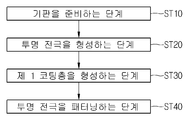
도 4를 참조하면, 실시예에 따른 터치 패널 제조방법은, 기판을 준비하는 단계(ST10); 투명 전극을 형성하는 단계(ST20); 제 1 코팅층을 형성하는 단계(ST30); 및 투명 전극을 패터닝하는 단계(ST40)을 포함한다.Referring to FIG. 4, a method of manufacturing a touch panel according to an embodiment includes preparing a substrate (ST10); Forming a transparent electrode (ST20); Forming a first coating layer (ST30); And patterning the transparent electrode (ST40).
상기 기판을 준비하는 단계(ST10)에서는, 유리 기판 또는 플라스틱 기판을 준비한다. 상기 기판은 유효 영역과 비유효 영역으로 구분될 수 있으며, 상기 비유효 영역에는 소정의 색을 가지는, 일례로 흑색을 가지는 물질을 도포할 수 있으며, 이에 의해 로고 등을 형성할 수 있다.In the step of preparing the substrate (ST10), a glass substrate or a plastic substrate is prepared. The substrate may be divided into a valid region and an ineffective region, and a material having a predetermined color, for example, black may be applied to the ineffective region, thereby forming a logo or the like.
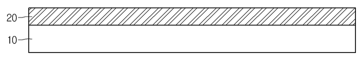
이어서, 상기 투명 전극을 형성하는 단계(ST20)에서는, 도 5에 도시되어 있듯이, 상기 기판(10) 상에 투명 전극(20) 형성 물질을 도포할 수 있다. 상기 투명 전극은 투명 전도성 물질을 포함할 수 있다. 일례로, 상기 투명 전도성 물질은 금속 나노 와이어를 포함할 수 있다. 바람직하게는, 상기 투명 전도성 물질은 구리, 알루미늄, 니켈, 주석, 아연, 금, 은 및 이들의 합금으로 이루어진 군에서 선택되는 물질을 적어도 하나 포함할 수 있다. 더 바람직하게는, 상기 투명 전도성 물질은 은 나노 와이어를 포함할 수 있다.Subsequently, in the step of forming the transparent electrode (ST20), as shown in FIG. 5, a material for forming the
상기 투명 전도성 물질은 다양한 방법으로 상기 기판 상에 형성될 수 있다. 일례로, 상기 투명 전도성 물질은 딥 코팅법에 의해 상기 기판 상에 형성될 수 있다. 그러나 실시예가 이에 한정되는 것은 아니며, 상기 투명 전도성 물질은 스핀(spin) 코팅, 플로우(flow) 코팅, 스프레이(spray) 코팅, 슬럿 다이(slot die) 코팅 및 롤(roll) 코팅 등의 다양한 코팅 방법으로 상기 기판 상에 코팅될 수 있다.The transparent conductive material may be formed on the substrate by various methods. In one example, the transparent conductive material may be formed on the substrate by a dip coating method. However, the embodiment is not limited thereto, and the transparent conductive material may be formed by various coating methods such as spin coating, flow coating, spray coating, slot die coating and roll coating May be coated on the substrate.
이어서, 상기 제 1 코팅층을 형성하는 단계(ST30)에서는, 도 6에 도시되어 있듯이, 상기 투명 전극(20) 상에 제 1 코팅층(40) 형성 물질을 도포할 수 있다. 상기 제 1 코팅층(40)은 절연 물질을 포함한다. 일례로, 상기 제 1 코팅층(40)은 아크릴수지, 우레탄 수지, 페놀 수지, 에폭시 수지 및 실란 수지 중 적어도 하나를 포함할 수 있다.Subsequently, in step ST30 of forming the first coating layer, a material for forming the
도 6에서는 편의상 상기 투명 전극(20) 상에 상기 코팅층(40)이 형성되는 것으로 도시하였으나, 상기 코팅층(40)은 상기 투명 전극(20) 상에 도포되면서, 상기 코팅층(40)과 상기 투명 전극(20)은 서로 혼재하여 위치할 수 있다. 즉, 상기 나노 와이어를 포함하는 상기 투명 전극(20)은 상기 코팅층(40)이 도포되면서, 상기 코팅층 상에 떠있는 상태로 될 수 있다. 즉, 상기 코팅층과 상기 투명 전극은 서로 섞이면서, 상기 투명 전극의 하부 및 상부 상에 코팅층이 불규칙적으로 도포되어 형성될 수 있다. 다시 말해, 상기 투명 전극은 상기 코팅층이 도포되면서, 상기 투명 전극층이 상기 코팅층 상부에 위치하거나, 상기 코팅층 상에 위치하는 투명 전극과 상기 코팅층 하부에 위치하는 투명 전극이 혼재하여 위치할 수 있다.6, the
이어서, 이어서, 상기 투명 전극을 패터닝하는 단계(ST40)에서는, 상기 투명 전극(20)을 패터닝할 수 있다. 즉, 도 7에 도시되어 있듯이, 상기 투명 전극을 일정한 모양으로 패터닝할 수 있다. 상기 투명 전극은 다양한 방법으로 패터닝될 수 있다. 일례로, 상기 투명 전극은 포토리소그래피 공법에 의해 패터닝될 수 있다. 즉, 노광, 현상 및 에칭 공정에 의해, 상기 투명 전극을 일정한 모양으로 패터닝할 수 있다. 이에 따라, 상기 투명 전극은 다수 개의 투명 전극들을 형성할 수 있다.Subsequently, in the step of patterning the transparent electrode (ST40), the
상기 투명 전극(20)과 상기 배선 전극(30)을 형성하는 공정은 동시에 수행될 수 있다. 즉, 상기 배선 전극은 상기 투명 전극(20)과 동일한 절연 물질을 포함할 수 있으며, 상기 패터닝 공정도 동시에 진행될 수 있다. 이에 따라, 도 8에 도시되어 있듯이, 상기 기판 상에는 패터닝된 다수 개의 투명 전극들 및 배선 전극들이 형성된다.The process of forming the
또한, 상기 패터닝 공정 후에는, 상기 제 1 코팅층은 상기 투명 전극 및/또는 상기 배선 전극 사이에 위치하며, 상기 투명 전극 및/또는 상기 배선 전극의 측면 전체 또는 측면의 일부분과 직접 접촉하며 배치된다.Further, after the patterning step, the first coating layer is disposed between the transparent electrode and / or the wiring electrode, and is disposed in direct contact with the transparent electrode and / or the entire side surface or a part of the side surface of the wiring electrode.
이어서, 도 9에 도시되어 있듯이, 상기 투명 전극(20) 상에 상기 제 2 코팅층을 형성될 수 있다 상기 제 2 코팅층(50)은 상기 제 1 코팅층과 동일한 물질을 포함할 수 있다. 즉, 상기 제 2 코팅층(50)은 아크릴수지, 우레탄 수지, 페놀 수지, 에폭시 수지 및 실란 수지 중 적어도 하나를 포함할 수 있다.Next, as shown in FIG. 9, the second coating layer may be formed on the
상기 제 2 코팅층(50)은 상기 투명 전극 상에 배치되어 상기 투명 전극의 산화를 방지할 수 있다.The
이어서, 도 9에 도시되어 있듯이, 상기 제 2 코팅층(50) 상에 접착층을 형성한 후, 상기 접착층(60)에 의해 터치 패널과 모듈(D)을 접착할 수 있다. 그러나, 상기 접착층을 형성하는 공정은 생략될 수 있다. 즉, 상기 접착층 대신 상기 제 2 코팅층이 산화방지층 및 접착층의 역할을 동시에 할 수 있다.
Next, as shown in FIG. 9, after the adhesive layer is formed on the
실시예에 따른 터치 패널 제조방법은, 상기 투명 전극을 패터닝하기 전에 상기 투명 전극 상에 제 1 코팅층을 형성한다. 즉, 상기 투명 전극 물질을 상기 기판 상에 도포한 후, 상기 투명 전극 물질 상에 상기 제 1 코팅층 형성 물질인 고분자 절연 수지를 도포한다.A method of manufacturing a touch panel according to an embodiment of the present invention includes forming a first coating layer on the transparent electrode before patterning the transparent electrode. That is, the transparent electrode material is coated on the substrate, and then the polymer insulating resin as the first coating layer forming material is coated on the transparent electrode material.
이에 따라, 상기 투명 전극 상에 도포되어 형성되는 상기 제 1 코팅층은 상기 기판과 상기 투명 전극의 밀착력을 강화함으로써, 이후에 형성되는 투명 전극의 패터닝 공정시 상기 투명 전극이 상기 기판에서 이탈되는 것을 방지할 수 있다.Accordingly, the first coating layer formed on the transparent electrode enhances adhesion between the substrate and the transparent electrode, thereby preventing the transparent electrode from being detached from the substrate during the patterning process of the transparent electrode to be formed later can do.
또한, 상기 패터닝 공정 후에도, 상기 제 2 코팅층은 상기 투명 전극들 사이에 배치됨으로써, 상기 기판과 상기 투명 전극의 밀착력을 향상시킴과 동시에, 상기 투명 전극들이 외부에 노출되었을 때, 투명 전극이 산화되는 것을 방지할 수 있다.Also, after the patterning process, the second coating layer is disposed between the transparent electrodes to improve adhesion between the substrate and the transparent electrodes, and when the transparent electrodes are exposed to the outside, the transparent electrodes are oxidized Can be prevented.
따라서, 실시예에 따른 터치 패널 제조방법은, 투명 전극을 기판 상에 형성한 후, 패터닝 공정을 진행하기 전에, 밀착력 강화 및 산화 방지 역할을 하는 제 1 코팅층을 형성함으로써, 투명 전극의 손상을 방지하고, 터치 패널의 신뢰도를 향상시킬 수 있다.
Therefore, in the method of manufacturing a touch panel according to the embodiment, after forming the transparent electrode on the substrate, the first coating layer serving to strengthen the adhesion and prevent oxidation is formed before the patterning process, And the reliability of the touch panel can be improved.
상술한 실시예에 설명된 특징, 구조, 효과 등은 본 발명의 적어도 하나의 실시예에 포함되며, 반드시 하나의 실시예에만 한정되는 것은 아니다. 나아가, 각 실시예에서 예시된 특징, 구조, 효과 등은 실시예들이 속하는 분야의 통상의 지식을 가지는 자에 의하여 다른 실시예들에 대해서도 조합 또는 변형되어 실시 가능하다. 따라서 이러한 조합과 변형에 관계된 내용들은 본 발명의 범위에 포함되는 것으로 해석되어야 할 것이다. The features, structures, effects and the like described in the foregoing embodiments are included in at least one embodiment of the present invention and are not necessarily limited to one embodiment. Further, the features, structures, effects, and the like illustrated in the embodiments may be combined or modified in other embodiments by those skilled in the art to which the embodiments belong. Therefore, it should be understood that the present invention is not limited to these combinations and modifications.
또한, 이상에서 실시예들을 중심으로 설명하였으나 이는 단지 예시일 뿐 본 발명을 한정하는 것이 아니며, 본 발명이 속하는 분야의 통상의 지식을 가진 자라면 본 실시예의 본질적인 특성을 벗어나지 않는 범위에서 이상에 예시되지 않은 여러 가지의 변형과 응용이 가능함을 알 수 있을 것이다. 예를 들어, 실시예들에 구체적으로 나타난 각 구성 요소는 변형하여 실시할 수 있는 것이다. 그리고 이러한 변형과 응용에 관계된 차이점들은 첨부한 청구 범위에서 규정하는 본 발명의 범위에 포함되는 것으로 해석되어야 할 것이다. While the present invention has been particularly shown and described with reference to exemplary embodiments thereof, it is clearly understood that the same is by way of illustration and example only and is not to be construed as limiting the scope of the present invention. It can be seen that various modifications and applications are possible. For example, each component specifically shown in the embodiments may be modified and implemented. It is to be understood that the present invention may be embodied in many other specific forms without departing from the spirit or essential characteristics thereof.
Claims (12)
상기 기판 상에 형성되는 투명 전극; 및
상기 기판 상에 형성되고, 상기 투명 전극의 측면과 직접 접촉하는 제 1 코팅층을 포함하는 터치 패널.Board;
A transparent electrode formed on the substrate; And
And a first coating layer formed on the substrate and in direct contact with a side surface of the transparent electrode.
상기 제 1 코팅층의 두께는 상기 투명 전극의 두께 이하인 터치 패널.The method according to claim 1,
Wherein a thickness of the first coating layer is equal to or less than a thickness of the transparent electrode.
상기 제 1 코팅층의 두께는 50㎚ 내지 200㎚인 터치 패널.3. The method of claim 2,
Wherein the thickness of the first coating layer is 50 nm to 200 nm.
상기 제 1 코팅층은 아크릴수지, 우레탄 수지, 페놀 수지, 에폭시 수지 및 실란 수지 중 적어도 하나를 포함하는 터치 패널.The method according to claim 1,
Wherein the first coating layer comprises at least one of an acrylic resin, a urethane resin, a phenol resin, an epoxy resin, and a silane resin.
상기 투명 전극 상에 형성되는 제 2 코팅층을 더 포함하는 터치 패널.The method according to claim 1,
And a second coating layer formed on the transparent electrode.
상기 제 1 코팅층 및 상기 제 2 코팅층은 아크릴수지, 우레탄 수지, 페놀 수지, 에폭시 수지 및 실란 수지 중 적어도 하나를 포함하는 터치 패널.6. The method of claim 5,
Wherein the first coating layer and the second coating layer comprise at least one of an acrylic resin, a urethane resin, a phenol resin, an epoxy resin, and a silane resin.
상기 투명 전극은 은(Ag) 나노 와이어를 포함하는 터치 패널.The method according to claim 6,
Wherein the transparent electrode comprises silver (Ag) nanowires.
상기 기판 상에 투명 전극 물질을 도포하여 투명 전극을 형성하는 단계;
상기 기판 상에 제 1 코팅층 물질을 도포하여 제 1 코팅층을 형성하는 단계; 및
상기 투명 전극을 패터닝하여 다수 개의 투명 전극들을 형성하는 단계를 포함하고,
상기 제 1 코팅층은 상기 투명 전극의 측면과 직접 접촉하며 형성되는 터치 패널 제조방법.Preparing a substrate;
Forming a transparent electrode by applying a transparent electrode material on the substrate;
Forming a first coating layer by applying a first coating material on the substrate; And
And patterning the transparent electrode to form a plurality of transparent electrodes,
Wherein the first coating layer is formed in direct contact with a side surface of the transparent electrode.
상기 제 1 코팅층은 상기 투명 전극의 두께 이하로 형성되는 터치 패널 제조방법.9. The method of claim 8,
Wherein the first coating layer is formed to have a thickness equal to or smaller than the thickness of the transparent electrode.
상기 제 1 코팅층은 50㎚ 내지 200㎚의 두께로 형성되는 터치 패널 제조방법.9. The method of claim 8,
Wherein the first coating layer is formed to a thickness of 50 nm to 200 nm.
상기 투명 전극 상에 형성되는 제 2 코팅층을 형성하는 단계를 더 포함하는 터치 패널 제조방법.10. The method of claim 9,
And forming a second coating layer on the transparent electrode.
상기 제 1 코팅층 및 상기 제 2 코팅층은 아크릴수지, 우레탄 수지, 페놀 수지, 에폭시 수지 및 실란 수지 중 적어도 하나를 포함하는 터치 패널 제조방법.11. The method of claim 10,
Wherein the first coating layer and the second coating layer comprise at least one of an acrylic resin, a urethane resin, a phenol resin, an epoxy resin, and a silane resin.
Priority Applications (1)
| Application Number | Priority Date | Filing Date | Title |
|---|---|---|---|
| KR1020120147829A KR20140078455A (en) | 2012-12-17 | 2012-12-17 | Touch panel and method of fabricating the same |
Applications Claiming Priority (1)
| Application Number | Priority Date | Filing Date | Title |
|---|---|---|---|
| KR1020120147829A KR20140078455A (en) | 2012-12-17 | 2012-12-17 | Touch panel and method of fabricating the same |
Publications (1)
| Publication Number | Publication Date |
|---|---|
| KR20140078455A true KR20140078455A (en) | 2014-06-25 |
Family
ID=51130066
Family Applications (1)
| Application Number | Title | Priority Date | Filing Date |
|---|---|---|---|
| KR1020120147829A KR20140078455A (en) | 2012-12-17 | 2012-12-17 | Touch panel and method of fabricating the same |
Country Status (1)
| Country | Link |
|---|---|
| KR (1) | KR20140078455A (en) |
Cited By (3)
| Publication number | Priority date | Publication date | Assignee | Title |
|---|---|---|---|---|
| KR20160127890A (en) * | 2015-04-27 | 2016-11-07 | 삼성디스플레이 주식회사 | Touch panel |
| KR20180060327A (en) * | 2016-11-28 | 2018-06-07 | 엘지디스플레이 주식회사 | Substrate embedded transparent conducting layer and method of fabricating the same, and electric device using the substrate |
| US10061463B2 (en) | 2015-03-04 | 2018-08-28 | Samsung Display Co., Ltd. | Touch panel and display device including the same |
-
2012
- 2012-12-17 KR KR1020120147829A patent/KR20140078455A/en not_active Application Discontinuation
Cited By (3)
| Publication number | Priority date | Publication date | Assignee | Title |
|---|---|---|---|---|
| US10061463B2 (en) | 2015-03-04 | 2018-08-28 | Samsung Display Co., Ltd. | Touch panel and display device including the same |
| KR20160127890A (en) * | 2015-04-27 | 2016-11-07 | 삼성디스플레이 주식회사 | Touch panel |
| KR20180060327A (en) * | 2016-11-28 | 2018-06-07 | 엘지디스플레이 주식회사 | Substrate embedded transparent conducting layer and method of fabricating the same, and electric device using the substrate |
Similar Documents
| Publication | Publication Date | Title |
|---|---|---|
| CN102405457B (en) | Touch actuated sensor configuration integrated with an OLED structure | |
| EP2746907B1 (en) | Touch display device and method of manufacturing the same | |
| KR101029490B1 (en) | Capacitive touch sensor integrated with window panel and mathod for manufacturing thereof | |
| US10091872B2 (en) | Touch window and display including the same | |
| TWI634471B (en) | Touch panel and touch device with the same | |
| JP3153971U (en) | Touchpad | |
| CN102622145A (en) | Projection type capacitive touch sensor structure and manufacturing method thereof | |
| JP2014149861A (en) | Touch panel and method for manufacturing the same | |
| US8947399B2 (en) | Dual-substrate capacitive touch panel | |
| JP2014529376A (en) | Thin film sensor, capacitive touch panel having the same, manufacturing method thereof and terminal product | |
| TW201606594A (en) | Conductive structure body and method for manufacturing the same, and display device | |
| US20150145791A1 (en) | Touch sensor module and manufacturing method thereof | |
| TWM354119U (en) | Improved capacitance touch sensor structure | |
| CN105103098B (en) | Contact panel, its preparation method and the silver-colored palladium neodymium alloy for contact panel | |
| KR20130128928A (en) | Touch panel and formation of electrode | |
| KR20140078455A (en) | Touch panel and method of fabricating the same | |
| US20150277604A1 (en) | Touch sensor module | |
| TWI486859B (en) | Capacitive touch panel structure | |
| KR20150145211A (en) | Window For Touch Panel And Touch Window Having It | |
| CN101719044A (en) | Capacitive touch screen and manufacturing method thereof | |
| KR101292361B1 (en) | Touch screen pannel and method for manufacturingthe same | |
| US20150090578A1 (en) | Touch panel and method of manufacturing the same | |
| TWI575281B (en) | Capacitive touch panel and manufacturing method thereof | |
| KR101025805B1 (en) | Capacitance type touch panel | |
| US20140247242A1 (en) | Touch screen panel |
Legal Events
| Date | Code | Title | Description |
|---|---|---|---|
| WITN | Application deemed withdrawn, e.g. because no request for examination was filed or no examination fee was paid |