KR20140052734A - Semiconductor device and method for fabricating the same - Google Patents
Semiconductor device and method for fabricating the same Download PDFInfo
- Publication number
- KR20140052734A KR20140052734A KR1020120119216A KR20120119216A KR20140052734A KR 20140052734 A KR20140052734 A KR 20140052734A KR 1020120119216 A KR1020120119216 A KR 1020120119216A KR 20120119216 A KR20120119216 A KR 20120119216A KR 20140052734 A KR20140052734 A KR 20140052734A
- Authority
- KR
- South Korea
- Prior art keywords
- region
- fin
- height
- pin
- isolation film
- Prior art date
Links
- 238000000034 method Methods 0.000 title claims description 43
- 239000004065 semiconductor Substances 0.000 title abstract description 39
- 238000002955 isolation Methods 0.000 claims abstract description 79
- 239000000758 substrate Substances 0.000 claims abstract description 54
- 230000001154 acute effect Effects 0.000 claims abstract description 25
- 238000005530 etching Methods 0.000 claims description 25
- 230000007423 decrease Effects 0.000 claims description 4
- 238000001312 dry etching Methods 0.000 claims description 4
- 238000000926 separation method Methods 0.000 claims description 3
- 230000015572 biosynthetic process Effects 0.000 claims 1
- 239000010410 layer Substances 0.000 description 25
- 239000000463 material Substances 0.000 description 15
- 229910052751 metal Inorganic materials 0.000 description 10
- 239000002184 metal Substances 0.000 description 10
- 238000004519 manufacturing process Methods 0.000 description 9
- XUIMIQQOPSSXEZ-UHFFFAOYSA-N Silicon Chemical compound [Si] XUIMIQQOPSSXEZ-UHFFFAOYSA-N 0.000 description 8
- 229910052710 silicon Inorganic materials 0.000 description 8
- 239000010703 silicon Substances 0.000 description 8
- 125000006850 spacer group Chemical group 0.000 description 8
- VYPSYNLAJGMNEJ-UHFFFAOYSA-N Silicium dioxide Chemical compound O=[Si]=O VYPSYNLAJGMNEJ-UHFFFAOYSA-N 0.000 description 6
- 229910052814 silicon oxide Inorganic materials 0.000 description 6
- 239000011229 interlayer Substances 0.000 description 5
- 229910052581 Si3N4 Inorganic materials 0.000 description 4
- 230000006870 function Effects 0.000 description 4
- HQVNEWCFYHHQES-UHFFFAOYSA-N silicon nitride Chemical compound N12[Si]34N5[Si]62N3[Si]51N64 HQVNEWCFYHHQES-UHFFFAOYSA-N 0.000 description 4
- 229910000577 Silicon-germanium Inorganic materials 0.000 description 3
- 239000012535 impurity Substances 0.000 description 3
- 238000003860 storage Methods 0.000 description 3
- 238000000231 atomic layer deposition Methods 0.000 description 2
- 238000005229 chemical vapour deposition Methods 0.000 description 2
- 238000010586 diagram Methods 0.000 description 2
- 238000005240 physical vapour deposition Methods 0.000 description 2
- JBRZTFJDHDCESZ-UHFFFAOYSA-N AsGa Chemical compound [As]#[Ga] JBRZTFJDHDCESZ-UHFFFAOYSA-N 0.000 description 1
- ZOXJGFHDIHLPTG-UHFFFAOYSA-N Boron Chemical compound [B] ZOXJGFHDIHLPTG-UHFFFAOYSA-N 0.000 description 1
- 229910001218 Gallium arsenide Inorganic materials 0.000 description 1
- 229910000673 Indium arsenide Inorganic materials 0.000 description 1
- GPXJNWSHGFTCBW-UHFFFAOYSA-N Indium phosphide Chemical compound [In]#P GPXJNWSHGFTCBW-UHFFFAOYSA-N 0.000 description 1
- OAICVXFJPJFONN-UHFFFAOYSA-N Phosphorus Chemical compound [P] OAICVXFJPJFONN-UHFFFAOYSA-N 0.000 description 1
- ATJFFYVFTNAWJD-UHFFFAOYSA-N Tin Chemical compound [Sn] ATJFFYVFTNAWJD-UHFFFAOYSA-N 0.000 description 1
- LEVVHYCKPQWKOP-UHFFFAOYSA-N [Si].[Ge] Chemical compound [Si].[Ge] LEVVHYCKPQWKOP-UHFFFAOYSA-N 0.000 description 1
- 238000007792 addition Methods 0.000 description 1
- 229910052782 aluminium Inorganic materials 0.000 description 1
- 238000013459 approach Methods 0.000 description 1
- 229910052785 arsenic Inorganic materials 0.000 description 1
- RQNWIZPPADIBDY-UHFFFAOYSA-N arsenic atom Chemical compound [As] RQNWIZPPADIBDY-UHFFFAOYSA-N 0.000 description 1
- 229910052796 boron Inorganic materials 0.000 description 1
- 239000000969 carrier Substances 0.000 description 1
- 230000000694 effects Effects 0.000 description 1
- 230000005669 field effect Effects 0.000 description 1
- VTGARNNDLOTBET-UHFFFAOYSA-N gallium antimonide Chemical compound [Sb]#[Ga] VTGARNNDLOTBET-UHFFFAOYSA-N 0.000 description 1
- 239000011521 glass Substances 0.000 description 1
- 238000011065 in-situ storage Methods 0.000 description 1
- WPYVAWXEWQSOGY-UHFFFAOYSA-N indium antimonide Chemical compound [Sb]#[In] WPYVAWXEWQSOGY-UHFFFAOYSA-N 0.000 description 1
- RPQDHPTXJYYUPQ-UHFFFAOYSA-N indium arsenide Chemical compound [In]#[As] RPQDHPTXJYYUPQ-UHFFFAOYSA-N 0.000 description 1
- 239000012212 insulator Substances 0.000 description 1
- 150000004767 nitrides Chemical class 0.000 description 1
- 229910052698 phosphorus Inorganic materials 0.000 description 1
- 239000011574 phosphorus Substances 0.000 description 1
- 229920002120 photoresistant polymer Polymers 0.000 description 1
- 229910021420 polycrystalline silicon Inorganic materials 0.000 description 1
- 229920005591 polysilicon Polymers 0.000 description 1
- 238000004528 spin coating Methods 0.000 description 1
- 150000003498 tellurium compounds Chemical class 0.000 description 1
- 229910052721 tungsten Inorganic materials 0.000 description 1
Images


Classifications
-
- H—ELECTRICITY
- H01—ELECTRIC ELEMENTS
- H01L—SEMICONDUCTOR DEVICES NOT COVERED BY CLASS H10
- H01L21/00—Processes or apparatus adapted for the manufacture or treatment of semiconductor or solid state devices or of parts thereof
- H01L21/02—Manufacture or treatment of semiconductor devices or of parts thereof
- H01L21/04—Manufacture or treatment of semiconductor devices or of parts thereof the devices having at least one potential-jump barrier or surface barrier, e.g. PN junction, depletion layer or carrier concentration layer
- H01L21/18—Manufacture or treatment of semiconductor devices or of parts thereof the devices having at least one potential-jump barrier or surface barrier, e.g. PN junction, depletion layer or carrier concentration layer the devices having semiconductor bodies comprising elements of Group IV of the Periodic System or AIIIBV compounds with or without impurities, e.g. doping materials
- H01L21/30—Treatment of semiconductor bodies using processes or apparatus not provided for in groups H01L21/20 - H01L21/26
- H01L21/302—Treatment of semiconductor bodies using processes or apparatus not provided for in groups H01L21/20 - H01L21/26 to change their surface-physical characteristics or shape, e.g. etching, polishing, cutting
- H01L21/306—Chemical or electrical treatment, e.g. electrolytic etching
- H01L21/308—Chemical or electrical treatment, e.g. electrolytic etching using masks
- H01L21/3083—Chemical or electrical treatment, e.g. electrolytic etching using masks characterised by their size, orientation, disposition, behaviour, shape, in horizontal or vertical plane
- H01L21/3086—Chemical or electrical treatment, e.g. electrolytic etching using masks characterised by their size, orientation, disposition, behaviour, shape, in horizontal or vertical plane characterised by the process involved to create the mask, e.g. lift-off masks, sidewalls, or to modify the mask, e.g. pre-treatment, post-treatment
-
- H—ELECTRICITY
- H01—ELECTRIC ELEMENTS
- H01L—SEMICONDUCTOR DEVICES NOT COVERED BY CLASS H10
- H01L21/00—Processes or apparatus adapted for the manufacture or treatment of semiconductor or solid state devices or of parts thereof
- H01L21/70—Manufacture or treatment of devices consisting of a plurality of solid state components formed in or on a common substrate or of parts thereof; Manufacture of integrated circuit devices or of parts thereof
- H01L21/71—Manufacture of specific parts of devices defined in group H01L21/70
- H01L21/76—Making of isolation regions between components
- H01L21/762—Dielectric regions, e.g. EPIC dielectric isolation, LOCOS; Trench refilling techniques, SOI technology, use of channel stoppers
- H01L21/7624—Dielectric regions, e.g. EPIC dielectric isolation, LOCOS; Trench refilling techniques, SOI technology, use of channel stoppers using semiconductor on insulator [SOI] technology
-
- H—ELECTRICITY
- H01—ELECTRIC ELEMENTS
- H01L—SEMICONDUCTOR DEVICES NOT COVERED BY CLASS H10
- H01L29/00—Semiconductor devices adapted for rectifying, amplifying, oscillating or switching, or capacitors or resistors with at least one potential-jump barrier or surface barrier, e.g. PN junction depletion layer or carrier concentration layer; Details of semiconductor bodies or of electrodes thereof ; Multistep manufacturing processes therefor
- H01L29/66—Types of semiconductor device ; Multistep manufacturing processes therefor
- H01L29/66007—Multistep manufacturing processes
- H01L29/66075—Multistep manufacturing processes of devices having semiconductor bodies comprising group 14 or group 13/15 materials
- H01L29/66227—Multistep manufacturing processes of devices having semiconductor bodies comprising group 14 or group 13/15 materials the devices being controllable only by the electric current supplied or the electric potential applied, to an electrode which does not carry the current to be rectified, amplified or switched, e.g. three-terminal devices
- H01L29/66409—Unipolar field-effect transistors
- H01L29/66477—Unipolar field-effect transistors with an insulated gate, i.e. MISFET
- H01L29/66787—Unipolar field-effect transistors with an insulated gate, i.e. MISFET with a gate at the side of the channel
- H01L29/66795—Unipolar field-effect transistors with an insulated gate, i.e. MISFET with a gate at the side of the channel with a horizontal current flow in a vertical sidewall of a semiconductor body, e.g. FinFET, MuGFET
-
- H—ELECTRICITY
- H01—ELECTRIC ELEMENTS
- H01L—SEMICONDUCTOR DEVICES NOT COVERED BY CLASS H10
- H01L29/00—Semiconductor devices adapted for rectifying, amplifying, oscillating or switching, or capacitors or resistors with at least one potential-jump barrier or surface barrier, e.g. PN junction depletion layer or carrier concentration layer; Details of semiconductor bodies or of electrodes thereof ; Multistep manufacturing processes therefor
- H01L29/66—Types of semiconductor device ; Multistep manufacturing processes therefor
- H01L29/68—Types of semiconductor device ; Multistep manufacturing processes therefor controllable by only the electric current supplied, or only the electric potential applied, to an electrode which does not carry the current to be rectified, amplified or switched
- H01L29/76—Unipolar devices, e.g. field effect transistors
- H01L29/772—Field effect transistors
- H01L29/78—Field effect transistors with field effect produced by an insulated gate
- H01L29/785—Field effect transistors with field effect produced by an insulated gate having a channel with a horizontal current flow in a vertical sidewall of a semiconductor body, e.g. FinFET, MuGFET
- H01L29/7853—Field effect transistors with field effect produced by an insulated gate having a channel with a horizontal current flow in a vertical sidewall of a semiconductor body, e.g. FinFET, MuGFET the body having a non-rectangular crossection
- H01L29/7854—Field effect transistors with field effect produced by an insulated gate having a channel with a horizontal current flow in a vertical sidewall of a semiconductor body, e.g. FinFET, MuGFET the body having a non-rectangular crossection with rounded corners
-
- H—ELECTRICITY
- H01—ELECTRIC ELEMENTS
- H01L—SEMICONDUCTOR DEVICES NOT COVERED BY CLASS H10
- H01L29/00—Semiconductor devices adapted for rectifying, amplifying, oscillating or switching, or capacitors or resistors with at least one potential-jump barrier or surface barrier, e.g. PN junction depletion layer or carrier concentration layer; Details of semiconductor bodies or of electrodes thereof ; Multistep manufacturing processes therefor
- H01L29/66—Types of semiconductor device ; Multistep manufacturing processes therefor
- H01L29/66007—Multistep manufacturing processes
- H01L29/66075—Multistep manufacturing processes of devices having semiconductor bodies comprising group 14 or group 13/15 materials
- H01L29/66227—Multistep manufacturing processes of devices having semiconductor bodies comprising group 14 or group 13/15 materials the devices being controllable only by the electric current supplied or the electric potential applied, to an electrode which does not carry the current to be rectified, amplified or switched, e.g. three-terminal devices
- H01L29/66409—Unipolar field-effect transistors
- H01L29/66477—Unipolar field-effect transistors with an insulated gate, i.e. MISFET
- H01L29/66545—Unipolar field-effect transistors with an insulated gate, i.e. MISFET using a dummy, i.e. replacement gate in a process wherein at least a part of the final gate is self aligned to the dummy gate
Landscapes
- Engineering & Computer Science (AREA)
- Microelectronics & Electronic Packaging (AREA)
- Power Engineering (AREA)
- General Physics & Mathematics (AREA)
- Computer Hardware Design (AREA)
- Physics & Mathematics (AREA)
- Condensed Matter Physics & Semiconductors (AREA)
- Manufacturing & Machinery (AREA)
- Ceramic Engineering (AREA)
- Insulated Gate Type Field-Effect Transistor (AREA)
- Thin Film Transistor (AREA)
- Element Separation (AREA)
- Metal-Oxide And Bipolar Metal-Oxide Semiconductor Integrated Circuits (AREA)
Abstract
Description
본 발명은 반도체 소자 및 이의 제조 방법에 관한 것이다.The present invention relates to a semiconductor device and a manufacturing method thereof.
반도체 장치의 밀도를 높이기 위한 스케일링(scaling) 기술 중 하나로서, 기판 상에 핀(fin) 형상의 실리콘 바디(body)를 형성하고 실리콘 바디의 표면 위에 게이트를 형성하는 멀티-게이트(multi-gate) 트랜지스터가 제안되었다. As one of scaling techniques for increasing the density of semiconductor devices, there is a multi-gate technique for forming a fin-shaped silicon body on a substrate and forming a gate on the surface of the silicon body. Transistors have been proposed.
이러한 멀티 게이트 트랜지스터는 3차원의 채널을 이용하기 때문에, 스케일링하는 것이 용이하다. 또한, 멀티 게이트 트랜지스터의 게이트 길이를 증가시키지 않아도, 전류 제어 능력을 향상시킬 수 있다. 뿐만 아니라, 드레인 전압에 의해 채널 영역의 전위가 영향을 받는 SCE(short channel effect)를 효과적으로 억제할 수 있다.Since such a multi-gate transistor uses a three-dimensional channel, scaling is easy. Further, the current control capability can be improved without increasing the gate length of the multi-gate transistor. In addition, the short channel effect (SCE) in which the potential of the channel region is affected by the drain voltage can be effectively suppressed.
본 발명이 해결하려는 과제는, 수직 핀과 테이퍼(tapered)진 핀을 결합한 하이브리드 핀을 사용하여, 핀의 밀도를 증가시킴과 동시에 누설 전류를 감소시킴으로써 신뢰성을 개선할 수 있는 반도체 소자를 제공하는 것이다. SUMMARY OF THE INVENTION A problem to be solved by the present invention is to provide a semiconductor device which can improve reliability by using a hybrid pin combining a vertical pin and a tapered pin to reduce the leakage current while increasing the density of the pin .
본 발명이 해결하려는 다른 과제는, 상기 반도체 소자를 제조하는 반도체 소자 제조 방법을 제공하는 것이다. Another object to be solved by the present invention is to provide a method of manufacturing a semiconductor device for manufacturing the semiconductor device.
본 발명이 해결하려는 과제들은 이상에서 언급한 과제들로 제한되지 않으며, 언급되지 않은 또 다른 과제들은 아래의 기재로부터 당업자에게 명확하게 이해될 수 있을 것이다. The problems to be solved by the present invention are not limited to the above-mentioned problems, and other matters not mentioned can be clearly understood by those skilled in the art from the following description.
상기 과제를 해결하기 위한 본 발명의 반도체 소자의 일 태양(aspect)은 기판, 상기 기판 상에 형성된 제1 핀, 및 상기 기판 상에 형성되고, 상기 제1 핀의 일부와 접촉하는 소자 분리막을 포함하고, 상기 제1 핀은 상기 소자 분리막과 접촉하는 제1 영역과, 상기 소자 분리막과 비접촉하는 제2 영역과, 상기 제1 영역과 상기 제2 영역 사이의 경계선을 포함하고, 상기 제1 영역은 상기 경계선을 중심으로 수직인 기울기를 갖고, 상기 제2 영역은 상기 경계선을 중심으로 예각인 기울기를 갖는다. According to an aspect of the present invention, there is provided a semiconductor device comprising a substrate, a first fin formed on the substrate, and an element isolation film formed on the substrate and in contact with a part of the first fin Wherein the first fin includes a first region in contact with the device isolation film, a second region in non-contact with the device isolation film, and a boundary line between the first region and the second region, The second region has a slope that is perpendicular to the boundary line, and the second region has an acute slope about the boundary line.
본 발명의 몇몇 실시예에서, 상기 소자 분리막의 상면은 상기 제1 핀에 가까운 제1 포인트와, 상기 제1 포인트보다 먼 제2 포인트를 포함하고, 상기 기판으로부터 상기 제1 포인트까지의 제1 높이와, 상기 기판으로부터 상기 제2 포인트까지의 제2 높이가 서로 다르다.In some embodiments of the present invention, the upper surface of the device isolation film includes a first point near the first fin and a second point farther from the first point, and the first height from the substrate to the first point And a second height from the substrate to the second point are different from each other.
본 발명의 몇몇 실시예에서, 상기 제1 높이는 상기 제2 높이보다 높다. In some embodiments of the present invention, the first height is higher than the second height.
본 발명의 몇몇 실시예에서, 상기 경계선에서, 상기 예각은 79도 내지 87도이다. In some embodiments of the present invention, at the boundary, the acute angle is between 79 degrees and 87 degrees.
본 발명의 몇몇 실시예에서, 상기 제1 핀의 상기 제2 영역의 상기 예각은 변한다. In some embodiments of the present invention, the acute angle of the second region of the first fin changes.
본 발명의 몇몇 실시예에서, 상기 예각은 상기 경계선으로부터 멀어질수록 작아진다. In some embodiments of the present invention, the acute angle decreases with distance from the boundary line.
본 발명의 몇몇 실시예에서, 상기 제1 핀의 상기 제2 영역은 콘 형상(cone type)을 포함한다. In some embodiments of the present invention, the second region of the first fin includes a cone type.
본 발명의 몇몇 실시예에서, 상기 기판으로부터 돌출되고, 상기 제1 핀과 인접하는 제2 핀을 더 포함하고, 상기 제1 핀과 상기 제2 핀 사이의 피치(pitch)에 대한 상기 제1 핀의 높이의 비율은 0.6 내지 1.2이다. In some embodiments of the present invention, the apparatus further comprises a second pin protruding from the substrate and adjacent to the first pin, the first pin having a pitch with respect to a pitch between the first pin and the second pin, Is 0.6 to 1.2.
본 발명의 몇몇 실시예에서, 상기 피치는 48nm 이하이다. In some embodiments of the invention, the pitch is 48 nm or less.
본 발명의 몇몇 실시예에서, 상기 제1 영역의 높이는 제1 높이이고, 상기 제2 영역의 높이는 제2 높이이고, 상기 제1 높이는 상기 제2 높이의 2배 내지 10배이다. In some embodiments of the present invention, the height of the first region is a first height, the height of the second region is a second height, and the first height is two to ten times the second height.
본 발명의 몇몇 실시예에서, 상기 제1 핀의 상기 제2 영역과 교차하는 게이트 전극을 더 포함하고, 상기 게이트 전극 양측의 상기 제1 핀 내에 형성되는 리세스를 더 포함하고, 상기 리세스 내에 형성되는 소오스/드레인 영역을 더 포함한다. In some embodiments of the present invention, the device further comprises a recess formed in the first fin on either side of the gate electrode, further comprising a gate electrode crossing the second region of the first fin, And a source / drain region to be formed.
상기 다른 과제를 해결하기 위한 본 발명의 반도체 소자 제조 방법의 일 태양은 수직인 기울기를 갖는 더미 핀을 기판 상에 형성하고, 상기 더미 핀의 주변을 둘러싸면서, 상기 더미 핀의 상면을 노출시키는 프리 소자 분리막을 형성하고, 상기 더미 핀과 상기 프리 소자 분리막을 식각하여, 수직인 기울기를 갖는 제1 영역과, 예각을 갖는 제2 영역과, 상기 제1 영역과 상기 제2 영역 사이의 경계선을 포함하는 핀을 형성하고, 상기 제1 영역과 접촉하는 소자 분리막을 형성하는 것을 포함된다. According to another aspect of the present invention, there is provided a method of manufacturing a semiconductor device, comprising: forming a dummy pin having a vertical inclination on a substrate; surrounding the periphery of the dummy pin; Etching the dummy pin and the free element separation film to form a device isolation film, etching the dummy pin and the free element separation film to form a first region having a vertical inclination, a second region having an acute angle, and a boundary line between the first region and the second region And forming an element isolation film in contact with the first region.
본 발명의 몇몇 실시예에서, 상기 핀과 상기 소자 분리막은 동시에 형성된다. In some embodiments of the present invention, the pin and the device isolation film are formed simultaneously.
본 발명의 몇몇 실시예에서, 상기 핀과 상기 소자 분리막을 형성하는 상기 식각은 건식 식각 공정을 포함한다. In some embodiments of the present invention, the etching for forming the pin and the device isolation film includes a dry etching process.
본 발명의 몇몇 실시예에서, 상기 제2 영역은 식각된 영역이고, 상기 제1 영역은 비식각된 영역이다. In some embodiments of the present invention, the second region is an etched region, and the first region is an un-etched region.
본 발명의 몇몇 실시예에서, 상기 핀과 상기 소자 분리막을 형성하는 것은 상기 프리 소자 분리막의 절반이 제거될 때까지 상기 더미 핀 및 상기 프리 소자 분리막을 식각하는 것을 포함한다. In some embodiments of the present invention, forming the pin and the device isolation film includes etching the dummy pin and the free element isolation film until half of the free element isolation film is removed.
본 발명의 기타 구체적인 사항들은 상세한 설명 및 도면들에 포함되어 있다. Other specific details of the invention are included in the detailed description and drawings.
도 1은 본 발명의 일 실시예에 따른 반도체 소자를 설명하기 위한 도면이다.
도 2는 도 1의 X를 확대한 도면이다.
도 3은 본 발명의 다른 실시예에 따른 반도체 소자를 설명하기 위한 도면이다.
도 4는 도 3의 YI를 확대한 도면이다.
도 5는 본 발명의 또 다른 실시예에 따른 반도체 소자를 설명하기 위한 도면이다.
도 6은 도 5의 AA를 자른 단면도이다.
도 7은 도 5의 BB를 자른 단면도이다.
도 8 내지 도 23은 본 발명의 일 실시예에 따른 반도체 소자 제조 방법을 설명하기 위한 중간 단계 도면들이다.
도 24은 본 발명의 몇몇 실시예에 따른 반도체 소자를 포함하는 전자 시스템의 블록도이다.
도 25 및 도 26은 본 발명의 몇몇 실시예들에 따른 반도체 소자를 적용할 수 있는 예시적인 반도체 시스템이다. 1 is a view for explaining a semiconductor device according to an embodiment of the present invention.
FIG. 2 is an enlarged view of FIG. 1; FIG.
3 is a view for explaining a semiconductor device according to another embodiment of the present invention.
4 is an enlarged view of YI in Fig.
5 is a view for explaining a semiconductor device according to another embodiment of the present invention.
6 is a cross-sectional view taken along line AA of FIG.
7 is a cross-sectional view taken along line BB of Fig.
FIGS. 8 to 23 are intermediate plan views illustrating a method of manufacturing a semiconductor device according to an embodiment of the present invention.
24 is a block diagram of an electronic system including a semiconductor device according to some embodiments of the present invention.
25 and 26 are exemplary semiconductor systems to which semiconductor devices according to some embodiments of the present invention may be applied.
본 발명의 이점 및 특징, 그리고 그것들을 달성하는 방법은 첨부되는 도면과 함께 상세하게 후술되어 있는 실시예들을 참조하면 명확해질 것이다. 그러나 본 발명은 이하에서 개시되는 실시예들에 한정되는 것이 아니라 서로 다른 다양한 형태로 구현될 것이며, 단지 본 실시예들은 본 발명의 개시가 완전하도록 하며, 본 발명이 속하는 기술분야에서 통상의 지식을 가진 자에게 발명의 범주를 완전하게 알려주기 위해 제공되는 것이며, 본 발명은 청구항의 범주에 의해 정의될 뿐이다. 도면에서 층 및 영역들의 상대적인 크기는 설명의 명료성을 위해 과장된 것일 수 있다. 명세서 전체에 걸쳐 동일 참조 부호는 동일 구성 요소를 지칭한다. BRIEF DESCRIPTION OF THE DRAWINGS The advantages and features of the present invention and the manner of achieving them will become apparent with reference to the embodiments described in detail below with reference to the accompanying drawings. The present invention may, however, be embodied in many different forms and should not be construed as being limited to the embodiments set forth herein. Rather, these embodiments are provided so that this disclosure will be thorough and complete, and will fully convey the scope of the invention to those skilled in the art. Is provided to fully convey the scope of the invention to those skilled in the art, and the invention is only defined by the scope of the claims. The relative sizes of layers and regions in the figures may be exaggerated for clarity of illustration. Like reference numerals refer to like elements throughout the specification.
하나의 소자(elements)가 다른 소자와 "접속된(connected to)" 또는 "커플링된(coupled to)" 이라고 지칭되는 것은, 다른 소자와 직접 연결 또는 커플링된 경우 또는 중간에 다른 소자를 개재한 경우를 모두 포함한다. 반면, 하나의 소자가 다른 소자와 "직접 접속된(directly connected to)" 또는 "직접 커플링된(directly coupled to)"으로 지칭되는 것은 중간에 다른 소자를 개재하지 않은 것을 나타낸다. 명세서 전체에 걸쳐 동일 참조 부호는 동일 구성 요소를 지칭한다. "및/또는"은 언급된 아이템들의 각각 및 하나 이상의 모든 조합을 포함한다. One element is referred to as being "connected to " or" coupled to "another element, either directly connected or coupled to another element, One case. On the other hand, when one element is referred to as being "directly connected to" or "directly coupled to " another element, it does not intervene another element in the middle. Like reference numerals refer to like elements throughout the specification. "And / or" include each and every combination of one or more of the mentioned items.
소자(elements) 또는 층이 다른 소자 또는 층의 "위(on)" 또는 "상(on)"으로 지칭되는 것은 다른 소자 또는 층의 바로 위뿐만 아니라 중간에 다른 층 또는 다른 소자를 개재한 경우를 모두 포함한다. 반면, 소자가 "직접 위(directly on)" 또는 "바로 위"로 지칭되는 것은 중간에 다른 소자 또는 층을 개재하지 않은 것을 나타낸다. It is to be understood that when an element or layer is referred to as being "on" or " on "of another element or layer, All included. On the other hand, a device being referred to as "directly on" or "directly above " indicates that no other device or layer is interposed in between.
비록 제1, 제2 등이 다양한 소자, 구성요소 및/또는 섹션들을 서술하기 위해서 사용되나, 이들 소자, 구성요소 및/또는 섹션들은 이들 용어에 의해 제한되지 않음은 물론이다. 이들 용어들은 단지 하나의 소자, 구성요소 또는 섹션들을 다른 소자, 구성요소 또는 섹션들과 구별하기 위하여 사용하는 것이다. 따라서, 이하에서 언급되는 제1 소자, 제1 구성요소 또는 제1 섹션은 본 발명의 기술적 사상 내에서 제2 소자, 제2 구성요소 또는 제2 섹션일 수도 있음은 물론이다. Although the first, second, etc. are used to describe various elements, components and / or sections, it is needless to say that these elements, components and / or sections are not limited by these terms. These terms are only used to distinguish one element, element or section from another element, element or section. Therefore, it goes without saying that the first element, the first element or the first section mentioned below may be the second element, the second element or the second section within the technical spirit of the present invention.
본 명세서에서 사용된 용어는 실시예들을 설명하기 위한 것이며 본 발명을 제한하고자 하는 것은 아니다. 본 명세서에서, 단수형은 문구에서 특별히 언급하지 않는 한 복수형도 포함한다. 명세서에서 사용되는 "포함한다(comprises)" 및/또는 "포함하는(comprising)"은 언급된 구성요소, 단계, 동작 및/또는 소자는 하나 이상의 다른 구성요소, 단계, 동작 및/또는 소자의 존재 또는 추가를 배제하지 않는다. The terminology used herein is for the purpose of illustrating embodiments and is not intended to be limiting of the present invention. In the present specification, the singular form includes plural forms unless otherwise specified in the specification. It is noted that the terms "comprises" and / or "comprising" used in the specification are intended to be inclusive in a manner similar to the components, steps, operations, and / Or additions.
다른 정의가 없다면, 본 명세서에서 사용되는 모든 용어(기술 및 과학적 용어를 포함)는 본 발명이 속하는 기술분야에서 통상의 지식을 가진 자에게 공통적으로 이해될 수 있는 의미로 사용될 수 있을 것이다. 또 일반적으로 사용되는 사전에 정의되어 있는 용어들은 명백하게 특별히 정의되어 있지 않는 한 이상적으로 또는 과도하게 해석되지 않는다. Unless defined otherwise, all terms (including technical and scientific terms) used herein may be used in a sense commonly understood by one of ordinary skill in the art to which this invention belongs. Also, commonly used predefined terms are not ideally or excessively interpreted unless explicitly defined otherwise.
이하에서, 도 1 및 도 2를 참조하여, 본 발명의 일 실시예에 따른 반도체 소자에 대해 설명한다. Hereinafter, a semiconductor device according to an embodiment of the present invention will be described with reference to FIGS. 1 and 2. FIG.
도 1은 본 발명의 일 실시예에 따른 반도체 소자를 설명하기 위한 도면이다. 도 2는 도 1의 I를 확대한 도면이다. 1 is a view for explaining a semiconductor device according to an embodiment of the present invention. 2 is an enlarged view of I in Fig.
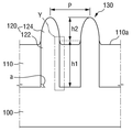
도 1을 참조하면, 반도체 소자는 기판(100), 제1 핀(120) 및 소자 분리막(110)을 포함할 수 있다. Referring to FIG. 1, a semiconductor device may include a
구체적으로, 기판(100)은 예를 들어, 벌크 실리콘 또는 SOI(silicon-on-insulator)일 수 있다. 이와 달리, 기판(100)은 실리콘 기판일 수도 있고, 또는 다른 물질, 예를 들어, 실리콘게르마늄, 안티몬화 인듐, 납 텔루르 화합물, 인듐 비소, 인듐 인화물, 갈륨 비소 또는 안티몬화 갈륨을 포함할 수 있다. 또는 기판(100)은 베이스 기판 상에 에피층이 형성된 것일 수도 있다. In particular, the
제1 핀(120)은 일방향을 따라서 길게 연장될 수 있다. 제1 핀(120)은 기판(100)의 일부일 수도 있고, 기판(100)으로부터 성장된 에피층(epitaxial layer)을 포함할 수 있다. 제1 핀(120)은 소자 분리막(110)을 기준으로 구분되는 제1 영역(122), 제2 영역(124) 및 경계선(120i)을 포함할 수 있다. 제1 핀(120)의 경계선(120i)은 제1 영역(122)과 제2 영역(124) 사이에 위치할 수 있고, 구체적으로, 제1 영역(122)과 제2 영역(124)의 경계면일 수 있다. 제1 핀(120)과 소자 분리막(110)의 위치 관계는 이후에 설명한다.The
소자 분리막(110)은 기판(100) 상에 형성될 수 있다. 소자 분리막(110)은 제1 핀(120)의 일부와 접촉되어 형성될 수 있다. 구체적으로, 소자 분리막(110)은 기판(100) 상에서 제1 핀(120)의 제1 영역(122)과 접촉하여 형성되고, 제1 핀(120)의 제2 영역(124)과 비접촉하여 형성될 수 있다. 소자 분리막(110)은 예를 들어, 실리콘 산화막, 실리콘 질화막, 실리콘 산화 질화막 중 적어도 하나를 포함할 수 있다.The
도 1 및 도 2를 참조하면, 제1 핀(120)의 제1 영역(122)의 기울기는 제1 기울기(a)를 가질 수 있다. 제1 기울기(a)는 제1 영역(122)의 측면과 기판 상면(100a)의 연장선이 이루는 각일 수 있고, 예를 들어, 수직일 수 있다. 다시 말하면, 제1 핀(120)의 제1 영역(122)은 경계선(120i)을 중심으로 수직인 기울기를 가질 수 있다. 여기서 "수직이다"라 함은 물리적으로 정확히 90도인 것뿐만 아니라, 제조 공정 상의 오차로 인하여 기울어진 것도 포함하는 의미이다. 본 발명의 실시예에 관한 설명에서, 제1 기울기(a)가 87도 내지 90도일 경우, 제1 기울기(a)는 수직인 것으로 본다. Referring to FIGS. 1 and 2, the slope of the
도 1 및 도 2를 참조하면, 제1 핀(120)의 제2 영역(124)은 경계선(120i)을 중심으로 예각인 기울기를 가질 수 있다. 여기서 "제2 영역은 예각을 갖는다"라 함은 제2 영역(124)의 임의의 점에서 그어진 접선과 경계선(120i)이 이루는 각이 예각이라는 것을 의미한다. 본 발명의 실시예에 관한 설명에서, "예각"은 87도보다 작은 각을 의미하는 것으로 설명한다. Referring to FIGS. 1 and 2, the
제1 핀(120)과 소자 분리막(110)이 만나는 지점은 경계점(O)일 수 있다. 경계점(O)는 제1 영역(122)과 제2 영역(124) 사이에 위치하는 경계선(120i) 상의 점이다. 경계선(120i)에서, 제2 영역(124)이 갖는 예각은 제2 기울기(b)일 수 있다. 제2 기울기(b)는 예를 들어, 79도 내지 87도의 값을 가질 수 있다. 구체적으로, 경계점(O)에서 그어진 접선과 경계선(120i)이 이루는 각은 제2 기울기(b)이다. 제2 기울기(b)는 예각이고, 예를 들어, 79도 내지 87도 사이의 각을 갖는다. The point where the
본 발명의 일 실시예에서, 경계선(120i)과 소자 분리막의 상면(110a)은 동일 평면상에 놓인다. 즉, 경계선(120i)의 연장선은 소자 분리막의 상면(110a)에 위치하게 된다. In one embodiment of the present invention, the
도 1 및 도 2를 참조하면, 제1 핀(120)의 제2 영역(124)과 경계선(120i)이 이루는 각은 변할 수 있다. 즉, 경계선(120i)을 중심으로 제2 영역(124)이 갖는 예각인 기울기는 변할 수 있다. Referring to FIGS. 1 and 2, the angle formed by the
예를 들어, 경계선(120i)을 중심으로 제2 영역(124)이 갖는 예각인 기울기는 경계선(120i)으로부터 멀어질수록 작아질 수 있다. 즉, 제2 영역(124)의 표면은 전체적으로 곡면으로 이뤄질 수 있다. 경계선(120i)으로부터 가장 멀리 떨어진 곳에서, 제2 영역(124)이 갖는 예각인 기울기는 0도일 수 있다. 즉, 경계선(120i)으로부터 가장 멀리 떨어진 곳에서, 제2 영역(124)의 접선은 경계선(120i)과 실질적으로 평행일 수 있다. 여기서 "평행이다"라 함은 임의의 두 지점 사이의 거리가 동일한 것뿐만 아니라, 제조 공정 상의 오차로 인하여 발생할 수 있는 미세한 거리의 차이를 포함하는 의미이다. 제1 핀(120)의 제2 영역(124)은 콘 형상(cone type)을 포함할 수 있고, 구체적으로 팁(tip) 부분이 라운딩된 콘 형상을 포함할 수 있다. For example, the slope, which is an acute angle of the
예를 들어, 제2 영역(124) 갖는 예각인 기울기는 경계선(120i)으로부터 일정 높이까지 일정한 제2 기울기(b)를 가지고, 그 후에는 경계선(120i)으로부터 멀어질수록 작아질 수 있다. 즉, 제2 영역(124)의 표면은 평면과 곡면의 조합으로 이뤄질 수 있다. 제2 기울기(b)를 갖는 부분까지의 제2 영역(124)의 표면은 평면이고, 그 후의 제2 영역(124)의 표면은 곡면일 수 있다. For example, the acute angle slope of the
도 1을 참조하면, 제1 핀(120)의 제1 영역(122)의 높이는 제1 높이(h1)이고, 제1 핀(120)의 제2 영역(124)의 높이는 제2 높이(h2)일 수 있다. 제1 높이(h1)은 소자 분리막(110)의 높이와 동일하다. 1, the height of the
제1 영역(122)의 제1 높이(h1)는 제2 영역(124)의 제2 높이(h2)보다 클 수 있다. 제2 영역(124)의 제2 높이(h2)에 대한 제1 영역(122)의 제1 높이(h1)의 비율은 2 내지 10일 수 있으나, 이에 제한되는 것은 아니다. 본 발명의 실시예들에 관한 설명에서, 제1 영역(122)의 제1 높이(h1)는 제2 영역(124)의 제2 높이(h2)의 2배인 것으로 설명한다. The first height h1 of the
도 1을 참조하면, 반도체 소자는 제2 핀(130)을 더 포함할 수 있다. 제2 핀(130)은 기판(100)으로부터 돌출되고, 제1 핀(120)과 인접되어 형성될 수 있다. 제2 핀(130)에 관한 설명은 제1 핀(120)과 중복되므로, 생략한다. Referring to FIG. 1, the semiconductor device may further include a
제1 핀(120)과 제2 핀(130) 사이의 거리는 피치(P)(pitch)라고 한다. 여기서, "피치"라 함은 인접하는 핀 사이의 간격이고, 구체적으로 인접하는 핀의 중심 사이의 거리를 의미한다. 본 발명의 실시예에서, 피치(P)는 제1 핀(120)의 제1 영역의 폭중심과 제2 핀(130)의 제1 영역의 폭중심 사이의 거리를 의미한다. The distance between the
제1 핀(120)과 제2 핀(130) 사이의 피치(P)에 대한 제1 핀(120)의 높이(h1+h2) 비율은 예를 들어, 0.6 내지 1.2 사이일 수 있다. 본 발명의 실시예에 관한 설명에서, 제2 영역(124)의 제2 높이(h2)에 대한 제1 영역(122)의 제1 높이(h1)의 비율은 2 내지 10일 수 있으므로, 제1 핀(120)과 제2 핀(130) 사이의 피치(P)는 제1 핀(120)의 제1 영역(122)의 제1 높이(h1)보다 작을 수 있다. The ratio of the height h1 + h2 of the
본 발명의 실시예에 관한 설명에서, 제1 핀(120)과 제2 핀(130) 사이의 피치(P)는 예를 들어, 48nm 이하일 수 있다. In the description of the embodiment of the present invention, the pitch P between the
도 3 및 도 4를 참조하여, 본 발명의 다른 실시예에 따른 반도체 소자를 설명하기 위한 도면이다. 본 실시예는 소자 분리막의 모양을 제외하고는 전술한 실시예와 실질적으로 동일하므로, 전술한 실시예와 중복되는 부분에 대하여는 동일한 도면부호를 기재하고 그에 대한 설명은 간략히 하거나 생략하기로 한다.3 and 4, a semiconductor device according to another embodiment of the present invention will be described. Since the present embodiment is substantially the same as the above embodiment except for the shape of the element isolation film, parts that are the same as those in the above embodiment will be denoted by the same reference numerals, and a description thereof will be simplified or omitted.
도 3은 본 발명의 다른 실시예에 따른 반도체 소자를 나타내는 도면이다. 도 4는 도 3의 II를 확대한 도면이다. 3 is a view showing a semiconductor device according to another embodiment of the present invention. 4 is an enlarged view of II in Fig.
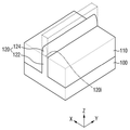
도 3을 참조하면, 반도체 소자는 기판(100), 제1 핀(120) 및 소자 분리막(110)을 포함할 수 있다. Referring to FIG. 3, the semiconductor device may include a
제1 영역(122), 제2 영역(124) 및 경계선(120i)을 포함하는 제1 핀(120)은 기판(100)으로부터 돌출되어 형성될 수 있다. 제1 핀(120)의 일부와 접촉되어 형성되는 소자 분리막(110)은 제1 핀(120)의 제1 영역(122)과 접촉하여 형성되고, 제1 핀(120)의 제2 영역(124)과 비접촉하여 형성될 수 있다. The
제1 핀(120)의 양측에 접하는 소자 분리막(110)은 제1 핀(120)과 제2 핀(130) 사이에 위치하는 소자 분리막(110)보다 돌출되어 있을 수 있다. 다시 말하면, 소자 분리막의 상면(110a)은 동일한 평면 상에 놓일 수 없고, 예를 들어, 기판 상면(100a)과 평행한 평면상에 놓일 수 없다. The
제1 핀(120)의 제1 영역(122)은 소자 분리막(110)과 접촉하여 형성되므로, 제1 핀(120)의 제1 영역(122)의 제1 높이(h1)은 기판 상면(100a)으로부터 돌출된 소자 분리막(110)까지의 거리이다. 제1 핀(120)의 제2 영역(124)의 제2 높이(h2)는 돌출된 소자 분리막(110)으로부터 제2 영역(124)의 팁 부분까지의 거리이다. The
도 3 및 도 4를 참조하면, 소자 분리막의 상면(110a)은 제1 포인트(S1) 및 제2 포인트(S2)를 포함할 수 있다. 제1 포인트(S1)은 제2 포인트(S2)보다 제1 핀(120)에서 가깝다. 기판 상면(100a)으로부터 제1 포인트(S1)까지의 거리는 제3 높이(h3)이고, 기판 상면(100a)으로부터 제2 포인트(S2)까지의 거리는 제4 높이(h4)일 수 있다. Referring to FIGS. 3 and 4, the
제1 포인트(S1)의 제3 높이(h3)는 제2 포인트(S2)의 제4 높이(h4)와 서로 다른 값을 가질 수 있다. 예를 들어, 소자 분리막의 상면(110a)은 제1 핀(120)에 근접함에 따라 돌출될 수 있으므로, 제1 포인트(S1)의 제3 높이(h3)는 제2 포인트(S2)의 제4 높이(h4)보다 높을 수 있다. The third height h3 of the first point S1 may have a different value from the fourth height h4 of the second point S2. For example, since the
도 3 및 도 4를 참조하면, 소자 분리막(110)은 제1 핀(120) 및 제2 핀(130)에 접하는 부분에 돌출부(110-1)를 포함할 수 있다. 즉, 소자 분리막(110)은 제1 핀(120) 및 제2 핀(130)에 접하는 부분은 돌출되고, 제1 핀(120)과 제2 핀(130)의 중간 부분은 평면일 수 있다. 하지만, 이와 같은 소자 분리막(110)의 모양은 본 발명의 실시예를 설명하기 위한 것일 뿐, 이에 제한되는 것은 아니다. 즉, 제1 핀(120) 및 제2 핀(130) 사이의 피치(P)가 충분히 이격되어 있을 경우, 소자 분리막의 상면(110a)은 제1 핀(120) 및 제2 핀(130) 사이에 평면을 포함할 수 있다. 하지만, 제1 핀(120) 및 제2 핀(130) 사이의 피치(P)가 작을 경우, 제1 핀(120)과 제2 핀(130) 사이의 소자 분리막(110)은 돌출부(110-1)만을 포함할 수 있다. 돌출부(110-1)는 제1 핀(120)의 제1 영역(122) 양측에 접하여 형성될 수 있다. Referring to FIGS. 3 and 4, the
소자 분리막의 상면(110a)이 제1 핀(120)과 제2 핀(130)의 중간 부분에 평면을 포함할 경우, 평면인 소자 분리막의 상면은 경계선(120i)보다 기판(100)으로부터 더 근접되어 있다. When the
도 5 내지 도 7을 참조하여, 본 발명의 또 다른 실시예에 따른 반도체 소자에 대해 설명한다. 본 실시예는 도 1에서 설명한 핀을 포함하는 핀형 트랜지스터이므로, 전술한 실시예와 중복되는 부분은 동일한 도면 부호를 기재하고, 설명은 간략히 하거나 생략한다. 5 to 7, a semiconductor device according to another embodiment of the present invention will be described. Since the present embodiment is a pin-type transistor including the pin described with reference to FIG. 1, the same elements as those of the above-described embodiment will be denoted by the same reference numerals, and a description thereof will be simplified or omitted.
도 5는 발명의 또 다른 실시예에 따른 반도체 소자를 설명하기 위한 도면이다. 도 6은 도 5의 AA를 자른 단면도이다. 도 7은 도 5의 BB를 자른 단면도이다. 5 is a view for explaining a semiconductor device according to another embodiment of the present invention. 6 is a cross-sectional view taken along line AA of FIG. 7 is a cross-sectional view taken along line BB of Fig.
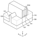
도 5 내지 도 7을 참조하면, 반도체 소자는 제1 핀(F1), 게이트 전극(147), 리세스(125), 소오스/드레인(161) 등을 포함할 수 있다. 5 to 7, the semiconductor device may include a first fin F1, a
제1 핀(120)은 제2 방향(Y1)을 따라서 길게 연장될 수 있다. 제1 핀(120)은 기판(100)의 일부일 수도 있고, 기판(101)으로부터 성장된 에피층(epitaxial layer)을 포함할 수 있다. 소자 분리막(110)은 제1 핀(120)의 측면을 덮을 수 있다.The
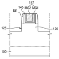
게이트 전극(147)은 제1 핀(120) 상에, 제1 핀(120)의 제2 영역(124)과 교차하도록 형성될 수 있다. 게이트 전극(147)은 제1 방향(X1)으로 연장될 수 있다. The
게이트 전극(147)은 금속층(MG1, MG2)을 포함할 수 있다. 게이트 전극(147)은 도시된 것과 같이, 2층 이상의 금속층(MG1, MG2)이 적층될 수 있다. 제1 금속층(MG1)은 일함수 조절을 하고, 제2 금속층(MG2)은 제1 금속층(MG1)에 의해 형성된 공간을 채우는 역할을 한다. 예를 들어, 제1 금속층(MG1) TiN, TaN, TiC, 및 TaC 중 적어도 하나를 포함할 수 있다. 또한, 제2 금속층(MG2)은 W 또는 Al을 포함할 수 있다. 또는, 게이트 전극(147)은 금속이 아닌, Si, SiGe 등으로 이루어질 수도 있다. 이러한 게이트 전극(147)은 예를 들어, 리플레이스먼트(replacement) 공정을 통해서 형성될 수 있으나, 이에 한정되는 것은 아니다.The
게이트 절연막(145)은 제1 핀(120)과 게이트 전극(147) 사이에 형성될 수 있다. 도 6에 도시된 것과 같이, 게이트 절연막(145)은 제1 핀(120)의 제2 영역(124)의 상부에 형성될 수 있다. 또한, 게이트 절연막(145)은 게이트 전극(147)과 소자 분리막(110) 사이에 배치될 수 있다. 이러한 게이트 절연막(145)은 실리콘 산화막보다 높은 유전 상수를 갖는 고유전체 물질을 포함할 수 있다. 예를 들어, 게이트 절연막(145)은 HfO2, ZrO2 또는 Ta2O5을 포함할 수 있다. A
리세스(125)는 게이트 전극(147) 양측의 제1 핀(120) 내에 형성될 수 있다. 리세스(125)의 측벽은 경사져 있어서, 리세스(125)의 형상은 기판(100)에서 멀어질수록 넓어질 수 있다. 도 5에 도시된 것처럼, 리세스(125)의 폭은 제1 핀(120)의 폭보다 넓을 수 있다. The
소오스/드레인(161)은 리세스(125) 내에 형성된다. 소오스/드레인(161)은 상승된(elevated) 소오스/드레인 형태일 수 있다. 즉, 소오스/드레인(161)의 상면은 층간 절연막(155)의 하면보다 높을 수 있다. 또한, 소오스/드레인(161)과 게이트 전극(147)은 스페이서(151)에 의하여 절연될 수 있다.The source /
반도체 소자가 PMOS 핀형 트랜지스터인 경우, 소오스/드레인(161)은 압축 스트레스 물질을 포함할 수 있다. 예를 들어, 압축 스트레스 물질은 Si에 비해서 격자상수가 큰 물질일 수 있고, 예를 들어 SiGe일 수 있다. 압축 스트레스 물질은 제1 핀(120)에 압축 스트레스를 가하여, 채널 영역의 캐리어인 홀(hole)의 이동도(mobility)를 향상시킬 수 있다. If the semiconductor device is a PMOS pin-type transistor, the source /
이와는 달리, 반도체 소자가 NMOS 핀형 트랜지스터인 경우, 소오스/드레인(161)은 기판(100)과 동일 물질 또는, 인장 스트레스 물질일 수 있다. 예를 들어, 기판(100)이 Si일 때, 소오스/드레인(161)은 Si이거나, Si보다 격자 상수가 작은 물질(예를 들어, SiC)일 수 있다. Alternatively, if the semiconductor device is an NMOS pinned transistor, the source /
스페이서(151)는 질화막, 산질화막 중 적어도 하나를 포함할 수 있다.The
도 5 내지 도 23을 참조하여, 본 발명의 일 실시예에 따른 반도체 소자 제조 방법에 대해서 설명한다. A method of manufacturing a semiconductor device according to an embodiment of the present invention will be described with reference to FIGS. 5 to 23. FIG.
도 8 내지 도 23은 본 발명의 일 실시예에 따른 반도체 소자 제조 방법을 설명하기 위한 중간 단계 도면들이다. 도 19는 도 18의 A-A를 따라서 절단한 단면도이고, 도 20는 도 18의 B-B를 따라서 절단한 단면도이다. 도 22는 도 21의 A-A를 따라서 절단한 단면도이고, 도 22는 도 21의 B-B를 따라서 절단한 단면도이다. FIGS. 8 to 23 are intermediate plan views illustrating a method of manufacturing a semiconductor device according to an embodiment of the present invention. Fig. 19 is a cross-sectional view taken along line A-A in Fig. 18, and Fig. 20 is a cross-sectional view taken along line B-B in Fig. 22 is a cross-sectional view taken along line A-A in Fig. 21, and Fig. 22 is a cross-sectional view taken along line B-B in Fig.
도 8을 참조하면, 기판(100) 상에 제1 마스크 패턴(201)이 형성될 수 있다. 제1 마스크 패턴(201)이 형성된 기판(100) 상에 제2 마스크막(205)이 형성될 수 있다. 제2 마스크막(205)는 제1 마스크 패턴(201)이 형성된 기판(100)의 상면을 실질적으로 컨포말하게(conformally) 형성될 수 있다. 제1 마스크 패턴(201)과 제2 마스크막(205)는 서로 간에 식각 선택성이 있는 물질을 포함할 수 있다. 예를 들어, 제2 마스크막(205)는 실리콘 산화물, 실리콘 질화물, 실리콘산화질화물, 금속막, 포토 레지스트(Photo Resist), 에스오지(SOG: Spin On Glass) 및/또는 에스오에이치(SOH: Spin On Hard mask) 중 적어도 하나를 포함할 수 있다. 제1 마스크 패턴(201)은 상기 물질들 중 제 2 마스크막(205)과 다른 물질로 형성될 수 있다. 제 1 마스크 패턴(201) 및 제 2 마스크막(205)은 물리 기상 증착 공정(Physical Vapor Deposition Process: PVD), 화학 기상 증착 공정(Chemical Vapor Deposition Process: CVD), 원자층 증착(Atomic Layer Deposition: ALD) 또는 스핀 코팅 방법 중에서 적어도 하나의 방식으로 형성될 수 있다. Referring to FIG. 8, a
도 9를 참조하면, 식각 공정에 의해 제2 마스크막(205)으로부터 제2 마스크 패턴(206)이 형성될 수 있다. 제 2 마스크 패턴(206)은 제 1 마스크 패턴(201)을 노출하는 스페이서 형태일 수 있다. 제 2 마스크 패턴(206)에 의하여 노출된 제 1 마스크 패턴(201)이 제거되어, 제2 마스크 패턴(206) 양측에 기판(100)이 노출될 수 있다. 제 1 마스크 패턴(201)의 제거는 제 2 마스크 패턴(206)의 식각을 최소화하며 제 1 마스크 패턴(201)을 제거할 수 있는 선택적 식각 공정을 포함할 수 있다. Referring to FIG. 9, a
도 10 및 도 11을 참조하면, 제2 마스크 패턴(206)을 식각 마스크로 이용하여, 기판(100)이 식각된다. 기판(100)의 일부가 식각됨으로써, 기판(100) 상에 더미 핀(120p)이 형성될 수 있다. 더미 핀(120p) 상에는 제2 마스크 패턴(206)이 남아있을 수 있다. 더미 핀(120p) 상에 남아 있는 제2 마스크 패턴(206)을 제거하여, 기판(100) 상에 돌출된 더미 핀(120p)이 형성될 수 있다. Referring to FIGS. 10 and 11, the
본 발명의 실시예에 대한 설명에서, 더미 핀(120p) 상의 제2 마스크 패턴(206)은 더미 핀(120p)을 감싸는 프리 소자 분리막(도 12의 110p)가 형성되기 전에 제거되는 것으로 설명하나, 이에 제한되는 것은 아니다. 즉, 제2 마스크 패턴(206)이 남아있는 더미 핀(120p) 상에 프리 소자 분리막을 형성한 후, 평탄화 공정을 통해 제2 마스크 패턴(206)이 제거될 수 있음은 물론이다. In the description of the embodiment of the present invention, the
더미 핀(120p)은 수직인 기울기를 가질 수 있다. 구체적으로, 더미 핀(120p)의 측면과 기판 상면(100a) 사이의 각은 수직일 수 있다. 제2 마스크 패턴(206)과 동일하게, 더미 핀(120p)은 제2 방향(Y)로 연장되어 형성될 수 있다. The
도 12를 참조하면, 기판(100) 상에 프리 소자 분리막(110p)이 형성된다. 프리 소자 분리막(110p)은 더미 핀(120p)의 주변을 둘러싸면서, 더미 핀(120p)의 상면을 노출시킨다. 프리 소자 분리막(110p)은 실리콘 산화막, 실리콘 질화막, 실리콘 산화 질화막 중 적어도 하나를 포함하는 물질로 형성될 수 있다. Referring to FIG. 12, a free
도 13a 및 도 13b를 참조하면, 식각 공정(300)에 의해, 프리 소자 분리막(110p) 및 더미 핀(120p)이 식각될 수 있다. 이를 통해, 기판(100) 상에 제1 핀(120) 및 소자 분리막(110)이 형성될 수 있다. 제1 핀(120)은 수직인 기울기를 갖는 제1 영역(122)과, 예각을 갖는 제2 영역(124)과, 제1 영역(122) 및 제2 영역(124) 사이의 경계선(120i)을 포함한다. 소자 분리막(110)은 제1 영역(122)과 접촉하여 형성되고, 제2 영역(124)과 비접촉하여 형성된다. Referring to FIGS. 13A and 13B, the free
프리 소자 분리막(110p) 및 더미 핀(120p)을 식각 하는 식각 공정(300)은 예를 들어, 건식 식각 공정을 포함할 수 있다. 본 발명의 실시예에 대한 설명에서, 식각 공정(300)은 건식 식각 공정으로 설명한다. The etching process 300 for etching the free
식각 공정(300)에 의해 프리 소자 분리막(110p) 및 더미 핀(120p)의 각각 높이는 점점 줄어들어, 제1 핀(120) 및 소자 분리막(110)이 동시에 형성될 수 있다. 구체적으로, 더미 핀(120p) 및 프리 소자 분리막(110p)에 각각 포함되는 물질은 서로 다르기 때문에, 더미 핀(120p) 및 프리 소자 분리막(110p)의 식각 가스에 대한 식각 선택비는 각각 다를 수 있다. 더미 핀(120p) 및 프리 소자 분리막(110p)을 함께 식각하여도, 더미 핀(120p) 및 프리 소자 분리막(110p)의 식각 정도는 다를 수 있다. 따라서, 소자 분리막(110) 상으로 돌출된 제1 핀(120)이 형성될 수 있다. The height of each of the free
제1 핀(120)의 제2 영역(124)은 식각 공정(300)에 의해 형성되는 부분이므로, 제2 영역(124)은 식각된 영역이다. 하지만, 제1 핀(120)의 제1 영역(122)은 소자 분리막(110)에 의해 감싸인 부분이고, 식각 공정(300)에 의해 식각된 부분이 아니므로, 제1 영역(122)은 식각 공정(300)에 의해 비식각된 부분이다. Since the
식각 공정(300)에 의해서 형성되는 부분인 제2 영역(124)은 경계선(120i)을 중심으로 예각인 기울기를 갖는다. 경계선(120i)에서 제2 영역(124)이 갖는 예각의 기울기는 79도 내지 87도일 수 있다. 경계선(120i)에서 제2 영역(124)이 갖는 예각의 기울기는 식각 공정(300)에 사용되는 식각 가스의 종류에 따라 변화될 수 있다. The
제1 영역(122)의 높이는 제2 영역(124)의 높이의 약 2 배 정도일 경우, 식각 공정(300)에 의해 프리 소자 분리막(110p)의 절반이 제거될 때까지, 더미 핀(120p) 및 프리 소자 분리막(110p)을 식각하여 제1 핀(120) 및 소자 분리막(110)이 형성될 수 있다. The height of the
또한, 제1 핀(120)에 문턱 전압 조절용 도핑이 수행될 수 있다. 반도체 소자가 NMOS 핀형 트랜지스터인 경우, 불순물은 붕소(B)일 수 있다. 반도체 소자가 PMOS 핀형 트랜지스터인 경우, 불순물은 인(P) 또는 비소(As)일 수 있다.Also, doping for threshold voltage adjustment may be performed on the first fin (120). If the semiconductor device is an NMOS finned transistor, the impurity may be boron (B). When the semiconductor element is a PMOS pin-type transistor, the impurity may be phosphorus (P) or arsenic (As).
도 14를 참조하여, 제3 마스크 패턴(2104)를 이용하여, 식각 공정을 진행하여, 제1 핀(120)과 교차하여 제1 방향(X)으로 연장되는 더미 게이트 절연막(141), 더미 게이트 전극(143)을 형성한다. Referring to FIG. 14, the
예를 들어, 더미 게이트 절연막(141)은 실리콘 산화막일 수 있고, 더미 게이트 전극(143)은 폴리 실리콘일 수 있다. For example, the dummy
도 15를 참조하면, 더미 게이트 전극(143)의 측벽 및 제1 핀(120)의 측벽에 제1 스페이서(151)가 형성된다. Referring to FIG. 15, a
예를 들어, 더미 게이트 전극(143)이 형성된 결과물 상에 절연막을 형성한 후 에치백 공정을 진행하여, 제1 스페이서(151)가 형성될 수 있다. 제1 스페이서(151)는 제3 마스크 패턴(2104)의 상면, 제1 핀(120)의 상면을 노출할 수 있다. 제1 스페이서(151)는 실리콘 질화막 또는 실리콘 산질화막일 수 있다.For example, after the insulating film is formed on the resultant product in which the
도 16을 참조하면, 제1 스페이서(151)가 형성된 결과물 상에, 층간 절연막(155)이 형성된다. 층간 절연막(155)은 예를 들어, 실리콘 산화막일 수 있다. Referring to FIG. 16, an
이어서, 더미 게이트 전극(143)의 상면이 노출될 때까지, 층간 절연막(155)을 평탄화한다. 그 결과, 제3 마스크 패턴(2104)이 제거되고 더미 게이트 전극(143)의 상면이 노출될 수 있다.Then, the
도 17을 참조하면, 더미 게이트 절연막(141) 및 더미 게이트 전극(143)이 제거된다. 더미 게이트 절연막(141) 및 더미 게이트 전극(143)의 제거됨에 따라, 소자 분리막(110)이 노출되는 트렌치(123)가 형성된다.Referring to FIG. 17, the dummy
도 18 내지 도 20을 참조하면, 트렌치(123) 내에 게이트 절연막(145) 및 게이트 전극(147)이 형성된다. Referring to FIGS. 18 to 20, a
게이트 절연막(145)은 트렌치(123)의 측벽 및 하면을 따라 실질적으로 컨포멀하게 형성될 수 있다. 게이트 절연막(145) 상에 금속층(MG1, MG2)을 포함하는 게이트 전극(147)이 형성될 수 있다. The
도 21 내지 도 23을 참조하면, 게이트 전극(147) 양측의 제1 핀(120) 내에 리세스(125)가 형성된다. Referring to FIGS. 21 to 23, recesses 125 are formed in the
리세스(125)는 게이트 전극(147) 양측의 핀(F1) 내에 형성될 수 있다. 리세스(125)의 측벽은 경사져 있어서, 리세스(125)의 형상은 기판(100)에서 멀어질수록 넓어질 수 있다. The
도 5 내지 도 7을 참조하면, 리세스(125) 내에 소오스/드레인(161)이 형성된다. 예를 들어, 소오스/드레인(161)은 소오스/드레인(161)의 상면은 층간 절연막(155)의 하면보다 높은 상승된(elevated) 소오스/드레인 형태일 수 있다. 5 to 7, a source /
소오스/드레인(161)을 형성하는 것은 에피택셜(epitaxial) 공정에 의해서 형성할 수 있다. 또한, 반도체 소자가 PMOS, NMOS 트랜지스터인지에 따라, 소오스/드레인(161)의 물질이 달라질 수 있다. 또한, 필요에 따라, 에피택셜 공정시 소오스/드레인(161)에 불순물을 인시츄(in-situ) 도핑할 수도 있다.The source /
도 24은 본 발명의 몇몇 실시예에 따른 반도체 소자를 포함하는 전자 시스템의 블록도이다. 24 is a block diagram of an electronic system including a semiconductor device according to some embodiments of the present invention.
도 24을 참조하면, 본 발명의 실시예에 따른 전자 시스템(1100)은 컨트롤러(1110), 입출력 장치(1120, I/O), 기억 장치(1130, memory device), 인터페이스(1140) 및 버스(1150, bus)를 포함할 수 있다. 컨트롤러(1110), 입출력 장치(1120), 기억 장치(1130) 및/또는 인터페이스(1140)는 버스(1150)를 통하여 서로 결합 될 수 있다. 버스(1150)는 데이터들이 이동되는 통로(path)에 해당한다.Referring to Figure 24, an
컨트롤러(1110)는 마이크로프로세서, 디지털 신호 프로세스, 마이크로 컨트롤러, 및 이들과 유사한 기능을 수행할 수 있는 논리 소자들 중에서 적어도 하나를 포함할 수 있다. 입출력 장치(1120)는 키패드(keypad), 키보드 및 디스플레이 장치 등을 포함할 수 있다. 기억 장치(1130)는 데이터 및/또는 명령어 등을 저장할 수 있다. 인터페이스(1140)는 통신 네트워크로 데이터를 전송하거나 통신 네트워크로부터 데이터를 수신하는 기능을 수행할 수 있다. 인터페이스(1140)는 유선 또는 무선 형태일 수 있다. 예컨대, 인터페이스(1140)는 안테나 또는 유무선 트랜시버 등을 포함할 수 있다. 도시하지 않았지만, 전자 시스템(1100)은 컨트롤러(1110)의 동작을 향상시키기 위한 동작 메모리로서, 고속의 디램 및/또는 에스램 등을 더 포함할 수도 있다. 본 발명의 실시예들에 따른 핀 전계효과 트랜지스터는 기억 장치(1130) 내에 제공되거나, 컨트롤러(1110), 입출력 장치(1120, I/O) 등의 일부로 제공될 수 있다. The
전자 시스템(1100)은 개인 휴대용 정보 단말기(PDA, personal digital assistant) 포터블 컴퓨터(portable computer), 웹 태블렛(web tablet), 무선 전화기(wireless phone), 모바일 폰(mobile phone), 디지털 뮤직 플레이어(digital music player), 메모리 카드(memory card), 또는 정보를 무선환경에서 송신 및/또는 수신할 수 있는 모든 전자 제품에 적용될 수 있다.
도 25 및 도 26은 본 발명의 몇몇 실시예들에 따른 반도체 소자를 적용할 수 있는 예시적인 반도체 시스템이다. 도 25은 태블릿 PC이고, 도 26은 노트북을 도시한 것이다. 본 발명의 실시예들에 따른 반도체 소자 중 적어도 하나는 태블릿 PC, 노트북 등에 사용될 수 있다. 본 발명의 몇몇 실시예들에 따른 반도체 장치는 예시하지 않는 다른 집적 회로 장치에도 적용될 수 있음은 당업자에게 자명하다.25 and 26 are exemplary semiconductor systems to which semiconductor devices according to some embodiments of the present invention may be applied. Fig. 25 shows a tablet PC, and Fig. 26 shows a notebook. At least one of the semiconductor devices according to the embodiments of the present invention can be used for a tablet PC, a notebook computer, and the like. It will be apparent to those skilled in the art that the semiconductor device according to some embodiments of the present invention may be applied to other integrated circuit devices not illustrated.
이상 첨부된 도면을 참조하여 본 발명의 실시예를 설명하였지만, 본 발명이 속하는 기술분야에서 통상의 지식을 가진 자는 본 발명이 그 기술적 사상이나 필수적인 특징을 변경하지 않고서 다른 구체적인 형태로 실시될 수 있다는 것을 이해할 수 있을 것이다. 그러므로 이상에서 기술한 실시예들은 모든 면에서 예시적인 것이며 한정적이 아닌 것으로 이해해야만 한다. While the present invention has been described in connection with what is presently considered to be practical exemplary embodiments, it is to be understood that the invention is not limited to the disclosed embodiments, but, on the contrary, You will understand. It is therefore to be understood that the above-described embodiments are illustrative in all aspects and not restrictive.
100: 기판 110: 소자 분리막
120: 제1 핀 122: 제1 핀의 제1 영역
124: 제1 핀의 제2 영역
120i: 제1 핀에서 제1 영역 및 제2 영역의 경계선100: substrate 110: element isolation film
120: first pin 122: first region of the first pin
124: second region of the first pin
120i: a boundary between the first region and the second region in the first fin
Claims (16)
상기 기판 상에 형성된 제1 핀; 및
상기 기판 상에 형성되고, 상기 제1 핀의 일부와 접촉하는 소자 분리막을 포함하고,
상기 제1 핀은 상기 소자 분리막과 접촉하는 제1 영역과, 상기 소자 분리막과 비접촉하는 제2 영역과, 상기 제1 영역과 상기 제2 영역 사이의 경계선을 포함하고,
상기 제1 영역은 상기 경계선을 중심으로 수직인 기울기를 갖고,
상기 제2 영역은 상기 경계선을 중심으로 예각인 기울기를 갖는 반도체 소자.Board;
A first fin formed on the substrate; And
And a device isolation film formed on the substrate and in contact with a part of the first fin,
Wherein the first fin includes a first region in contact with the device isolation film, a second region in non-contact with the device isolation film, and a boundary line between the first region and the second region,
Wherein the first region has a slope perpendicular to the boundary line,
And the second region has a slope at an acute angle with respect to the boundary line.
상기 소자 분리막의 상면은 상기 제1 핀에 가까운 제1 포인트와, 상기 제1 포인트보다 먼 제2 포인트를 포함하고,
상기 기판으로부터 상기 제1 포인트까지의 제1 높이와, 상기 기판으로부터 상기 제2 포인트까지의 제2 높이가 서로 다른 반도체 소자.The method according to claim 1,
Wherein an upper surface of the device isolation film includes a first point near the first fin and a second point farther from the first point,
Wherein a first height from the substrate to the first point and a second height from the substrate to the second point are different.
상기 제1 높이는 상기 제2 높이보다 높은 반도체 소자.3. The method of claim 2,
Wherein the first height is higher than the second height.
상기 경계선에서, 상기 예각은 79도 내지 87도인 반도체 소자.The method according to claim 1,
Wherein, at the boundary, the acute angle is from 79 degrees to 87 degrees.
상기 제1 핀의 상기 제2 영역의 상기 예각은 변하는 반도체 소자.The method according to claim 1,
Wherein the acute angle of the second region of the first fin is varied.
상기 예각은 상기 경계선으로부터 멀어질수록 작아지는 반도체 소자.6. The method of claim 5,
And the acute angle decreases as the distance from the boundary line decreases.
상기 제1 핀의 상기 제2 영역은 콘 형상(cone type)을 포함하는 반도체 소자.The method according to claim 6,
Wherein the second region of the first fin comprises a cone type.
상기 기판으로부터 돌출되고, 상기 제1 핀과 인접하는 제2 핀을 더 포함하고,
상기 제1 핀과 상기 제2 핀 사이의 피치(pitch)에 대한 상기 제1 핀의 높이의 비율은 0.6 내지 1.2인 반도체 소자.The method according to claim 1,
Further comprising a second pin protruding from the substrate and adjacent to the first pin,
Wherein a ratio of a height of the first fin to a pitch between the first fin and the second fin is 0.6 to 1.2.
상기 피치는 48nm 이하인 반도체 소자.9. The method of claim 8,
Wherein the pitch is 48 nm or less.
상기 제1 영역의 높이는 제1 높이이고, 상기 제2 영역의 높이는 제2 높이이고,
상기 제1 높이는 상기 제2 높이의 2배 내지 10배인 반도체 소자.The method according to claim 1,
The height of the first region is a first height, the height of the second region is a second height,
Wherein the first height is two to ten times the second height.
상기 제1 핀의 상기 제2 영역과 교차하는 게이트 전극을 더 포함하고,
상기 게이트 전극 양측의 상기 제1 핀 내에 형성되는 리세스를 더 포함하고,
상기 리세스 내에 형성되는 소오스/드레인 영역을 더 포함하는 반도체 소자.The method according to claim 1,
And a gate electrode crossing the second region of the first fin,
And a recess formed in the first fin on both sides of the gate electrode,
And a source / drain region formed in the recess.
상기 더미 핀의 주변을 둘러싸면서, 상기 더미 핀의 상면을 노출시키는 프리 소자 분리막을 형성하고,
상기 더미 핀과 상기 프리 소자 분리막을 식각하여, 수직인 기울기를 갖는 제1 영역과, 예각을 갖는 제2 영역과, 상기 제1 영역과 상기 제2 영역 사이의 경계선을 포함하는 핀을 형성하고, 상기 제1 영역과 접촉하는 소자 분리막을 형성하는 것을 포함하는 반도체 소자 제조 방법.A dummy pin having a vertical inclination is formed on the substrate,
Forming a free element isolation film which surrounds the periphery of the dummy pin and exposes an upper surface of the dummy pin,
Etching the dummy pin and the free element separation film to form a fin including a first region having a vertical inclination, a second region having an acute angle, and a boundary line between the first region and the second region, And forming an element isolation film in contact with the first region.
상기 핀과 상기 소자 분리막은 동시에 형성되는 반도체 소자 제조 방법.13. The method of claim 12,
Wherein the pin and the device isolation film are simultaneously formed.
상기 핀과 상기 소자 분리막을 형성하는 상기 식각은 건식 식각 공정을 포함하는 반도체 소자 제조 방법.13. The method of claim 12,
Wherein the etching for forming the pin and the device isolation film includes a dry etching process.
상기 제2 영역은 식각된 영역이고, 상기 제1 영역은 비식각된 영역인 반도체 소자 제조 방법.13. The method of claim 12,
Wherein the second region is an etched region and the first region is an un-etched region.
상기 핀과 상기 소자 분리막을 형성하는 것은
상기 프리 소자 분리막의 절반이 제거될 때까지 상기 더미 핀 및 상기 프리 소자 분리막을 식각하는 것을 포함하는 반도체 소자 제조 방법.13. The method of claim 12,
The formation of the pin and the element isolation film
And etching the dummy pin and the free element isolation layer until half of the free element isolation layer is removed.
Priority Applications (5)
| Application Number | Priority Date | Filing Date | Title |
|---|---|---|---|
| KR1020120119216A KR20140052734A (en) | 2012-10-25 | 2012-10-25 | Semiconductor device and method for fabricating the same |
| US14/034,787 US20140117426A1 (en) | 2012-10-25 | 2013-09-24 | Semiconductor device and method for fabricating the same |
| DE102013111548.9A DE102013111548A1 (en) | 2012-10-25 | 2013-10-21 | Semiconductor device and method for manufacturing the same |
| TW102138361A TW201417297A (en) | 2012-10-25 | 2013-10-24 | Semiconductor device and method for fabricating the same |
| CN201310511980.7A CN103779394A (en) | 2012-10-25 | 2013-10-25 | Semiconductor device and method for fabricating the same |
Applications Claiming Priority (1)
| Application Number | Priority Date | Filing Date | Title |
|---|---|---|---|
| KR1020120119216A KR20140052734A (en) | 2012-10-25 | 2012-10-25 | Semiconductor device and method for fabricating the same |
Publications (1)
| Publication Number | Publication Date |
|---|---|
| KR20140052734A true KR20140052734A (en) | 2014-05-07 |
Family
ID=50479822
Family Applications (1)
| Application Number | Title | Priority Date | Filing Date |
|---|---|---|---|
| KR1020120119216A KR20140052734A (en) | 2012-10-25 | 2012-10-25 | Semiconductor device and method for fabricating the same |
Country Status (5)
| Country | Link |
|---|---|
| US (1) | US20140117426A1 (en) |
| KR (1) | KR20140052734A (en) |
| CN (1) | CN103779394A (en) |
| DE (1) | DE102013111548A1 (en) |
| TW (1) | TW201417297A (en) |
Families Citing this family (21)
| Publication number | Priority date | Publication date | Assignee | Title |
|---|---|---|---|---|
| US9054044B2 (en) * | 2013-03-07 | 2015-06-09 | Globalfoundries Inc. | Method for forming a semiconductor device and semiconductor device structures |
| US9263554B2 (en) | 2013-06-04 | 2016-02-16 | International Business Machines Corporation | Localized fin width scaling using a hydrogen anneal |
| GB2529953B (en) * | 2013-06-28 | 2020-04-01 | Intel Corp | Nanostructures and nanofeatures with Si (111) planes on Si (100) wafers for III-N epitaxy |
| CN104425264B (en) * | 2013-08-20 | 2017-06-13 | 中芯国际集成电路制造(上海)有限公司 | The forming method of semiconductor structure |
| US9136131B2 (en) * | 2013-11-04 | 2015-09-15 | Globalfoundries Inc. | Common fill of gate and source and drain contacts |
| US9362404B2 (en) | 2014-02-21 | 2016-06-07 | Taiwan Semiconductor Manufacturing Company, Ltd. | Doping for FinFET |
| US9490346B2 (en) | 2014-06-12 | 2016-11-08 | Taiwan Semiconductor Manufacturing Co., Ltd. | Structure and formation method of fin-like field effect transistor |
| US9490365B2 (en) | 2014-06-12 | 2016-11-08 | Taiwan Semiconductor Manufacturing Co., Ltd. | Structure and formation method of fin-like field effect transistor |
| US9502538B2 (en) | 2014-06-12 | 2016-11-22 | Taiwan Semiconductor Manufacturing Co., Ltd | Structure and formation method of fin-like field effect transistor |
| US9842182B2 (en) * | 2014-10-01 | 2017-12-12 | Samsung Electronics Co., Ltd. | Method and system for designing semiconductor device |
| US9666716B2 (en) | 2014-12-15 | 2017-05-30 | Sang U. Kim | FinFET transistor |
| KR102262827B1 (en) * | 2014-12-30 | 2021-06-08 | 삼성전자주식회사 | Semiconductor device and the fabricating method thereof |
| KR102327143B1 (en) | 2015-03-03 | 2021-11-16 | 삼성전자주식회사 | Integrated circuit device |
| CN106206692B (en) * | 2015-04-30 | 2019-09-27 | 中芯国际集成电路制造(上海)有限公司 | The forming method of N-type fin formula field effect transistor |
| US10147805B2 (en) * | 2015-07-31 | 2018-12-04 | Taiwan Semiconductor Manufacturing Co., Ltd | Structure and formation method of semiconductor device structure with a dummy fin structure |
| KR102336787B1 (en) * | 2015-08-11 | 2021-12-07 | 삼성전자주식회사 | Semiconductor device |
| CN106449761B (en) * | 2016-11-30 | 2019-05-31 | 上海华力微电子有限公司 | The forming method of semiconductor devices |
| US9799570B1 (en) * | 2017-02-13 | 2017-10-24 | International Business Machines Corporation | Fabrication of vertical field effect transistors with uniform structural profiles |
| CN109524302B (en) * | 2017-09-20 | 2020-12-15 | 华邦电子股份有限公司 | Semiconductor assembly and its manufacturing method |
| US11276651B2 (en) * | 2020-05-18 | 2022-03-15 | Globalfoundries U.S. Inc. | IC product comprising a single active fin FinFET device and an electrically inactive fin stress reduction structure |
| US11600717B2 (en) * | 2020-05-20 | 2023-03-07 | Taiwan Semiconductor Manufacturing Co., Ltd | Dummy FIN profile control to enlarge gate process window |
Family Cites Families (5)
| Publication number | Priority date | Publication date | Assignee | Title |
|---|---|---|---|---|
| US8987092B2 (en) * | 2008-04-28 | 2015-03-24 | Spansion Llc | Methods for fabricating memory cells having fin structures with semicircular top surfaces and rounded top corners and edges |
| US9401784B2 (en) | 2009-10-21 | 2016-07-26 | Qualcomm Incorporated | Time and frequency acquisition and tracking for OFDMA wireless systems |
| US8629512B2 (en) * | 2012-03-28 | 2014-01-14 | Taiwan Semiconductor Manufacturing Company, Ltd. | Gate stack of fin field effect transistor with slanted sidewalls |
| US8883570B2 (en) * | 2012-07-03 | 2014-11-11 | Taiwan Semiconductor Manufacturing Company, Ltd. | Multi-gate FETs and methods for forming the same |
| US8669167B1 (en) * | 2012-08-28 | 2014-03-11 | International Business Machines Corporation | Techniques for metal gate workfunction engineering to enable multiple threshold voltage FINFET devices |
-
2012
- 2012-10-25 KR KR1020120119216A patent/KR20140052734A/en not_active Application Discontinuation
-
2013
- 2013-09-24 US US14/034,787 patent/US20140117426A1/en not_active Abandoned
- 2013-10-21 DE DE102013111548.9A patent/DE102013111548A1/en not_active Withdrawn
- 2013-10-24 TW TW102138361A patent/TW201417297A/en unknown
- 2013-10-25 CN CN201310511980.7A patent/CN103779394A/en active Pending
Also Published As
| Publication number | Publication date |
|---|---|
| TW201417297A (en) | 2014-05-01 |
| CN103779394A (en) | 2014-05-07 |
| US20140117426A1 (en) | 2014-05-01 |
| DE102013111548A1 (en) | 2014-04-30 |
Similar Documents
| Publication | Publication Date | Title |
|---|---|---|
| KR20140052734A (en) | Semiconductor device and method for fabricating the same | |
| US9627542B2 (en) | Semiconductor device and method for fabricating the same | |
| US10269928B2 (en) | Semiconductor devices having 3D channels, and methods of fabricating semiconductor devices having 3D channels | |
| US9443935B2 (en) | Method of fabricating fin-field effect transistors (finFETs) having different fin widths | |
| US9281208B2 (en) | Methods of forming semiconductor devices using hard mask layers | |
| KR20150118878A (en) | Semiconductor device and fabricated method thereof | |
| KR20150000546A (en) | Semiconductor device and method for fabricating the same | |
| KR20160035650A (en) | Semiconductor device and method of manufacturing the same | |
| KR20150125333A (en) | Semiconductor device and method for fabricating the same | |
| KR20140088419A (en) | Field effect transistor | |
| KR20130119213A (en) | Field effect transistor | |
| KR20140148189A (en) | Semiconductor device and method for fabricating the same | |
| KR102030329B1 (en) | Semiconductor device and method for fabricating the same | |
| KR102350001B1 (en) | Fabricating method of semiconductor device | |
| US20150132908A1 (en) | Method for fabricating semiconductor device | |
| KR20150111807A (en) | Semiconductor device and method for fabricating the same | |
| KR102059828B1 (en) | Semiconductor device and method for fabricating the same | |
| US9559192B1 (en) | Method of fabricating semiconductor device | |
| KR20150121907A (en) | Semiconductor device and method for fabricating the same | |
| KR102174144B1 (en) | Semiconductor device and method for fabricating the same | |
| KR102003276B1 (en) | Method for fabricating semiconductor device | |
| KR101994079B1 (en) | Semiconductor device and fabricated method thereof | |
| KR20170001529A (en) | Semiconductor device and method for fabricating the same | |
| US10008493B2 (en) | Semiconductor device and method of fabricating the same | |
| KR102321373B1 (en) | Method for fabricating semiconductor device |
Legal Events
| Date | Code | Title | Description |
|---|---|---|---|
| WITN | Application deemed withdrawn, e.g. because no request for examination was filed or no examination fee was paid |