KR20130139882A - Dual-layer method of fabricating ultracapacitor current collectors - Google Patents
Dual-layer method of fabricating ultracapacitor current collectors Download PDFInfo
- Publication number
- KR20130139882A KR20130139882A KR1020137007383A KR20137007383A KR20130139882A KR 20130139882 A KR20130139882 A KR 20130139882A KR 1020137007383 A KR1020137007383 A KR 1020137007383A KR 20137007383 A KR20137007383 A KR 20137007383A KR 20130139882 A KR20130139882 A KR 20130139882A
- Authority
- KR
- South Korea
- Prior art keywords
- layer
- formulation
- current collector
- graphite
- forming
- Prior art date
Links
- 238000004519 manufacturing process Methods 0.000 title abstract description 16
- 239000002355 dual-layer Substances 0.000 title 1
- OKTJSMMVPCPJKN-UHFFFAOYSA-N Carbon Chemical compound [C] OKTJSMMVPCPJKN-UHFFFAOYSA-N 0.000 claims abstract description 141
- 239000000203 mixture Substances 0.000 claims abstract description 110
- 238000009472 formulation Methods 0.000 claims abstract description 103
- 239000000758 substrate Substances 0.000 claims abstract description 74
- 239000006229 carbon black Substances 0.000 claims abstract description 73
- 238000000034 method Methods 0.000 claims abstract description 68
- 229910002804 graphite Inorganic materials 0.000 claims abstract description 66
- 239000010439 graphite Substances 0.000 claims abstract description 66
- 239000002131 composite material Substances 0.000 claims description 27
- 239000000463 material Substances 0.000 claims description 21
- 239000003623 enhancer Substances 0.000 claims description 13
- 239000007770 graphite material Substances 0.000 claims description 13
- 239000007787 solid Substances 0.000 claims description 12
- 238000001035 drying Methods 0.000 claims description 11
- XLYOFNOQVPJJNP-UHFFFAOYSA-N water Substances O XLYOFNOQVPJJNP-UHFFFAOYSA-N 0.000 claims description 11
- 239000002245 particle Substances 0.000 claims description 8
- 239000006260 foam Substances 0.000 abstract 1
- 239000010410 layer Substances 0.000 description 200
- 229910052799 carbon Inorganic materials 0.000 description 19
- 239000011248 coating agent Substances 0.000 description 16
- 238000000576 coating method Methods 0.000 description 16
- 239000011230 binding agent Substances 0.000 description 13
- 239000008367 deionised water Substances 0.000 description 10
- 229910021641 deionized water Inorganic materials 0.000 description 10
- 229920000036 polyvinylpyrrolidone Polymers 0.000 description 8
- 235000013855 polyvinylpyrrolidone Nutrition 0.000 description 8
- -1 alloys Chemical compound 0.000 description 7
- 239000006185 dispersion Substances 0.000 description 7
- 229910052751 metal Inorganic materials 0.000 description 7
- 239000002184 metal Substances 0.000 description 7
- 229920001343 polytetrafluoroethylene Polymers 0.000 description 6
- 239000004810 polytetrafluoroethylene Substances 0.000 description 6
- 239000000725 suspension Substances 0.000 description 6
- 230000015572 biosynthetic process Effects 0.000 description 5
- 229920001940 conductive polymer Polymers 0.000 description 5
- 229910021389 graphene Inorganic materials 0.000 description 5
- 238000002156 mixing Methods 0.000 description 5
- 239000002033 PVDF binder Substances 0.000 description 4
- 229920003171 Poly (ethylene oxide) Polymers 0.000 description 4
- 229910052782 aluminium Inorganic materials 0.000 description 4
- XAGFODPZIPBFFR-UHFFFAOYSA-N aluminium Chemical compound [Al] XAGFODPZIPBFFR-UHFFFAOYSA-N 0.000 description 4
- 239000011324 bead Substances 0.000 description 4
- 239000002041 carbon nanotube Substances 0.000 description 4
- 229910021393 carbon nanotube Inorganic materials 0.000 description 4
- 230000000052 comparative effect Effects 0.000 description 4
- 239000011370 conductive nanoparticle Substances 0.000 description 4
- 238000010790 dilution Methods 0.000 description 4
- 239000012895 dilution Substances 0.000 description 4
- 239000002071 nanotube Substances 0.000 description 4
- 229920000058 polyacrylate Polymers 0.000 description 4
- 239000011118 polyvinyl acetate Substances 0.000 description 4
- 229920002981 polyvinylidene fluoride Polymers 0.000 description 4
- 239000001267 polyvinylpyrrolidone Substances 0.000 description 4
- 238000007764 slot die coating Methods 0.000 description 4
- KFZMGEQAYNKOFK-UHFFFAOYSA-N Isopropanol Chemical compound CC(C)O KFZMGEQAYNKOFK-UHFFFAOYSA-N 0.000 description 3
- 230000009977 dual effect Effects 0.000 description 3
- PXHVJJICTQNCMI-UHFFFAOYSA-N Nickel Chemical compound [Ni] PXHVJJICTQNCMI-UHFFFAOYSA-N 0.000 description 2
- 239000004698 Polyethylene Substances 0.000 description 2
- 239000004743 Polypropylene Substances 0.000 description 2
- 238000010276 construction Methods 0.000 description 2
- 238000010586 diagram Methods 0.000 description 2
- 239000011888 foil Substances 0.000 description 2
- 150000002739 metals Chemical class 0.000 description 2
- BASFCYQUMIYNBI-UHFFFAOYSA-N platinum Chemical compound [Pt] BASFCYQUMIYNBI-UHFFFAOYSA-N 0.000 description 2
- 229920000573 polyethylene Polymers 0.000 description 2
- 229920001155 polypropylene Polymers 0.000 description 2
- 229920002635 polyurethane Polymers 0.000 description 2
- 239000004814 polyurethane Substances 0.000 description 2
- 229920002689 polyvinyl acetate Polymers 0.000 description 2
- 230000000717 retained effect Effects 0.000 description 2
- 239000000243 solution Substances 0.000 description 2
- RYGMFSIKBFXOCR-UHFFFAOYSA-N Copper Chemical compound [Cu] RYGMFSIKBFXOCR-UHFFFAOYSA-N 0.000 description 1
- ZOKXTWBITQBERF-UHFFFAOYSA-N Molybdenum Chemical compound [Mo] ZOKXTWBITQBERF-UHFFFAOYSA-N 0.000 description 1
- BQCADISMDOOEFD-UHFFFAOYSA-N Silver Chemical compound [Ag] BQCADISMDOOEFD-UHFFFAOYSA-N 0.000 description 1
- 229910000831 Steel Inorganic materials 0.000 description 1
- 239000004809 Teflon Substances 0.000 description 1
- 229920006362 Teflon® Polymers 0.000 description 1
- ATJFFYVFTNAWJD-UHFFFAOYSA-N Tin Chemical compound [Sn] ATJFFYVFTNAWJD-UHFFFAOYSA-N 0.000 description 1
- RTAQQCXQSZGOHL-UHFFFAOYSA-N Titanium Chemical compound [Ti] RTAQQCXQSZGOHL-UHFFFAOYSA-N 0.000 description 1
- 241000282485 Vulpes vulpes Species 0.000 description 1
- 239000011149 active material Substances 0.000 description 1
- 239000000654 additive Substances 0.000 description 1
- 239000000956 alloy Substances 0.000 description 1
- 229910045601 alloy Inorganic materials 0.000 description 1
- 229910021383 artificial graphite Inorganic materials 0.000 description 1
- 238000003490 calendering Methods 0.000 description 1
- 239000003990 capacitor Substances 0.000 description 1
- OKTJSMMVPCPJKN-YPZZEJLDSA-N carbon-10 atom Chemical class [10C] OKTJSMMVPCPJKN-YPZZEJLDSA-N 0.000 description 1
- 239000003575 carbonaceous material Substances 0.000 description 1
- 239000000919 ceramic Substances 0.000 description 1
- 150000001875 compounds Chemical class 0.000 description 1
- 239000010949 copper Substances 0.000 description 1
- 229910052802 copper Inorganic materials 0.000 description 1
- 238000007766 curtain coating Methods 0.000 description 1
- 238000003618 dip coating Methods 0.000 description 1
- 239000002270 dispersing agent Substances 0.000 description 1
- 230000005611 electricity Effects 0.000 description 1
- 239000011521 glass Substances 0.000 description 1
- PCHJSUWPFVWCPO-UHFFFAOYSA-N gold Chemical compound [Au] PCHJSUWPFVWCPO-UHFFFAOYSA-N 0.000 description 1
- 229910052737 gold Inorganic materials 0.000 description 1
- 239000010931 gold Substances 0.000 description 1
- 239000008187 granular material Substances 0.000 description 1
- 238000013038 hand mixing Methods 0.000 description 1
- 229910003437 indium oxide Inorganic materials 0.000 description 1
- PJXISJQVUVHSOJ-UHFFFAOYSA-N indium(iii) oxide Chemical compound [O-2].[O-2].[O-2].[In+3].[In+3] PJXISJQVUVHSOJ-UHFFFAOYSA-N 0.000 description 1
- 238000002347 injection Methods 0.000 description 1
- 239000007924 injection Substances 0.000 description 1
- 239000011810 insulating material Substances 0.000 description 1
- 150000002500 ions Chemical class 0.000 description 1
- 238000003475 lamination Methods 0.000 description 1
- 239000007788 liquid Substances 0.000 description 1
- 238000005259 measurement Methods 0.000 description 1
- 238000000691 measurement method Methods 0.000 description 1
- 229910052750 molybdenum Inorganic materials 0.000 description 1
- 239000011733 molybdenum Substances 0.000 description 1
- 229910021382 natural graphite Inorganic materials 0.000 description 1
- 229910052759 nickel Inorganic materials 0.000 description 1
- 238000007747 plating Methods 0.000 description 1
- 229910052697 platinum Inorganic materials 0.000 description 1
- 229920000642 polymer Polymers 0.000 description 1
- 239000000843 powder Substances 0.000 description 1
- 238000003825 pressing Methods 0.000 description 1
- 238000004080 punching Methods 0.000 description 1
- 239000002904 solvent Substances 0.000 description 1
- 239000010935 stainless steel Substances 0.000 description 1
- 229910001220 stainless steel Inorganic materials 0.000 description 1
- 239000010959 steel Substances 0.000 description 1
- 238000003860 storage Methods 0.000 description 1
- 239000000126 substance Substances 0.000 description 1
- 230000009897 systematic effect Effects 0.000 description 1
- 238000010345 tape casting Methods 0.000 description 1
- 239000011135 tin Substances 0.000 description 1
- 229910052718 tin Inorganic materials 0.000 description 1
- 239000010936 titanium Substances 0.000 description 1
- 229910052719 titanium Inorganic materials 0.000 description 1
- 231100000331 toxic Toxicity 0.000 description 1
- 230000002588 toxic effect Effects 0.000 description 1
- WFKWXMTUELFFGS-UHFFFAOYSA-N tungsten Chemical compound [W] WFKWXMTUELFFGS-UHFFFAOYSA-N 0.000 description 1
- 229910052721 tungsten Inorganic materials 0.000 description 1
- 239000010937 tungsten Substances 0.000 description 1
Images
Classifications
-
- H—ELECTRICITY
- H01—ELECTRIC ELEMENTS
- H01G—CAPACITORS; CAPACITORS, RECTIFIERS, DETECTORS, SWITCHING DEVICES, LIGHT-SENSITIVE OR TEMPERATURE-SENSITIVE DEVICES OF THE ELECTROLYTIC TYPE
- H01G11/00—Hybrid capacitors, i.e. capacitors having different positive and negative electrodes; Electric double-layer [EDL] capacitors; Processes for the manufacture thereof or of parts thereof
- H01G11/74—Terminals, e.g. extensions of current collectors
-
- H—ELECTRICITY
- H01—ELECTRIC ELEMENTS
- H01G—CAPACITORS; CAPACITORS, RECTIFIERS, DETECTORS, SWITCHING DEVICES, LIGHT-SENSITIVE OR TEMPERATURE-SENSITIVE DEVICES OF THE ELECTROLYTIC TYPE
- H01G11/00—Hybrid capacitors, i.e. capacitors having different positive and negative electrodes; Electric double-layer [EDL] capacitors; Processes for the manufacture thereof or of parts thereof
- H01G11/22—Electrodes
- H01G11/26—Electrodes characterised by their structure, e.g. multi-layered, porosity or surface features
- H01G11/28—Electrodes characterised by their structure, e.g. multi-layered, porosity or surface features arranged or disposed on a current collector; Layers or phases between electrodes and current collectors, e.g. adhesives
-
- H—ELECTRICITY
- H01—ELECTRIC ELEMENTS
- H01G—CAPACITORS; CAPACITORS, RECTIFIERS, DETECTORS, SWITCHING DEVICES, LIGHT-SENSITIVE OR TEMPERATURE-SENSITIVE DEVICES OF THE ELECTROLYTIC TYPE
- H01G11/00—Hybrid capacitors, i.e. capacitors having different positive and negative electrodes; Electric double-layer [EDL] capacitors; Processes for the manufacture thereof or of parts thereof
- H01G11/22—Electrodes
- H01G11/30—Electrodes characterised by their material
- H01G11/32—Carbon-based
-
- H—ELECTRICITY
- H01—ELECTRIC ELEMENTS
- H01G—CAPACITORS; CAPACITORS, RECTIFIERS, DETECTORS, SWITCHING DEVICES, LIGHT-SENSITIVE OR TEMPERATURE-SENSITIVE DEVICES OF THE ELECTROLYTIC TYPE
- H01G11/00—Hybrid capacitors, i.e. capacitors having different positive and negative electrodes; Electric double-layer [EDL] capacitors; Processes for the manufacture thereof or of parts thereof
- H01G11/66—Current collectors
- H01G11/70—Current collectors characterised by their structure
-
- H—ELECTRICITY
- H01—ELECTRIC ELEMENTS
- H01G—CAPACITORS; CAPACITORS, RECTIFIERS, DETECTORS, SWITCHING DEVICES, LIGHT-SENSITIVE OR TEMPERATURE-SENSITIVE DEVICES OF THE ELECTROLYTIC TYPE
- H01G11/00—Hybrid capacitors, i.e. capacitors having different positive and negative electrodes; Electric double-layer [EDL] capacitors; Processes for the manufacture thereof or of parts thereof
- H01G11/84—Processes for the manufacture of hybrid or EDL capacitors, or components thereof
-
- H—ELECTRICITY
- H01—ELECTRIC ELEMENTS
- H01G—CAPACITORS; CAPACITORS, RECTIFIERS, DETECTORS, SWITCHING DEVICES, LIGHT-SENSITIVE OR TEMPERATURE-SENSITIVE DEVICES OF THE ELECTROLYTIC TYPE
- H01G9/00—Electrolytic capacitors, rectifiers, detectors, switching devices, light-sensitive or temperature-sensitive devices; Processes of their manufacture
- H01G9/0029—Processes of manufacture
-
- Y—GENERAL TAGGING OF NEW TECHNOLOGICAL DEVELOPMENTS; GENERAL TAGGING OF CROSS-SECTIONAL TECHNOLOGIES SPANNING OVER SEVERAL SECTIONS OF THE IPC; TECHNICAL SUBJECTS COVERED BY FORMER USPC CROSS-REFERENCE ART COLLECTIONS [XRACs] AND DIGESTS
- Y02—TECHNOLOGIES OR APPLICATIONS FOR MITIGATION OR ADAPTATION AGAINST CLIMATE CHANGE
- Y02E—REDUCTION OF GREENHOUSE GAS [GHG] EMISSIONS, RELATED TO ENERGY GENERATION, TRANSMISSION OR DISTRIBUTION
- Y02E60/00—Enabling technologies; Technologies with a potential or indirect contribution to GHG emissions mitigation
- Y02E60/10—Energy storage using batteries
-
- Y—GENERAL TAGGING OF NEW TECHNOLOGICAL DEVELOPMENTS; GENERAL TAGGING OF CROSS-SECTIONAL TECHNOLOGIES SPANNING OVER SEVERAL SECTIONS OF THE IPC; TECHNICAL SUBJECTS COVERED BY FORMER USPC CROSS-REFERENCE ART COLLECTIONS [XRACs] AND DIGESTS
- Y02—TECHNOLOGIES OR APPLICATIONS FOR MITIGATION OR ADAPTATION AGAINST CLIMATE CHANGE
- Y02E—REDUCTION OF GREENHOUSE GAS [GHG] EMISSIONS, RELATED TO ENERGY GENERATION, TRANSMISSION OR DISTRIBUTION
- Y02E60/00—Enabling technologies; Technologies with a potential or indirect contribution to GHG emissions mitigation
- Y02E60/13—Energy storage using capacitors
-
- Y—GENERAL TAGGING OF NEW TECHNOLOGICAL DEVELOPMENTS; GENERAL TAGGING OF CROSS-SECTIONAL TECHNOLOGIES SPANNING OVER SEVERAL SECTIONS OF THE IPC; TECHNICAL SUBJECTS COVERED BY FORMER USPC CROSS-REFERENCE ART COLLECTIONS [XRACs] AND DIGESTS
- Y02—TECHNOLOGIES OR APPLICATIONS FOR MITIGATION OR ADAPTATION AGAINST CLIMATE CHANGE
- Y02T—CLIMATE CHANGE MITIGATION TECHNOLOGIES RELATED TO TRANSPORTATION
- Y02T10/00—Road transport of goods or passengers
- Y02T10/60—Other road transportation technologies with climate change mitigation effect
- Y02T10/70—Energy storage systems for electromobility, e.g. batteries
-
- Y—GENERAL TAGGING OF NEW TECHNOLOGICAL DEVELOPMENTS; GENERAL TAGGING OF CROSS-SECTIONAL TECHNOLOGIES SPANNING OVER SEVERAL SECTIONS OF THE IPC; TECHNICAL SUBJECTS COVERED BY FORMER USPC CROSS-REFERENCE ART COLLECTIONS [XRACs] AND DIGESTS
- Y10—TECHNICAL SUBJECTS COVERED BY FORMER USPC
- Y10T—TECHNICAL SUBJECTS COVERED BY FORMER US CLASSIFICATION
- Y10T29/00—Metal working
- Y10T29/49—Method of mechanical manufacture
- Y10T29/49002—Electrical device making
- Y10T29/49108—Electric battery cell making
- Y10T29/4911—Electric battery cell making including sealing
-
- Y—GENERAL TAGGING OF NEW TECHNOLOGICAL DEVELOPMENTS; GENERAL TAGGING OF CROSS-SECTIONAL TECHNOLOGIES SPANNING OVER SEVERAL SECTIONS OF THE IPC; TECHNICAL SUBJECTS COVERED BY FORMER USPC CROSS-REFERENCE ART COLLECTIONS [XRACs] AND DIGESTS
- Y10—TECHNICAL SUBJECTS COVERED BY FORMER USPC
- Y10T—TECHNICAL SUBJECTS COVERED BY FORMER US CLASSIFICATION
- Y10T29/00—Metal working
- Y10T29/49—Method of mechanical manufacture
- Y10T29/49002—Electrical device making
- Y10T29/49108—Electric battery cell making
- Y10T29/49114—Electric battery cell making including adhesively bonding
Landscapes
- Engineering & Computer Science (AREA)
- Power Engineering (AREA)
- Microelectronics & Electronic Packaging (AREA)
- Manufacturing & Machinery (AREA)
- Chemical & Material Sciences (AREA)
- Materials Engineering (AREA)
- Cell Electrode Carriers And Collectors (AREA)
- Battery Electrode And Active Subsutance (AREA)
- Electric Double-Layer Capacitors Or The Like (AREA)
- Laminated Bodies (AREA)
Abstract
다층 전류 컬렉터 제조방법은 제1포뮬레이션으로부터 전류 컬렉터 기판(103)의 각각의 주면에 걸쳐 제1층(104)을 형성하는 단계, 제2포뮬레이션으로부터 각각의 제1층(104)에 걸쳐 제2층(105)을 형성하는 단계를 포함하며, 상기 제1포뮬레이션 및 제2포뮬레이션 중 어느 하나는 흑연 포뮬레이션이고, 상기 제1포뮬레이션 및 제2포뮬레이션 중 또 다른 하나는 카본블랙 포뮬레이션이다.The multi-layer current collector fabrication method includes forming a first layer 104 over each major surface of the current collector substrate 103 from the first formulation, and over each first layer 104 from the second formulation. Forming a two-layer 105, wherein one of the first and second formulations is a graphite formulation and another one of the first and second formulations is a carbon black foam. It's emulation.
Description
본 출원은 35 U.S.C. §120 하에 2010년 8월 23일 출원된 미국출원 제12/860,995호의 우선권의 이점을 청구하며, 그와 관련된 내용들은 전체적으로 참조에 의해 여기에 반영된다.This application claims the benefit of 35 U.S.C. Claims the priority of U.S. Application No. 12 / 860,995, filed August 23, 2010, filed under §120, the contents of which are hereby incorporated by reference in their entirety.
본 발명은 전류 컬렉터 제조방법, 특히 울트라캐패시터 전극 제조방법에 관한 것이다. 특히, 본 발명은 제1포뮬레이션(first formulation)으로부터 전류 컬렉터 기판의 각각의 주면에 걸쳐 제1층을 형성하는 단계, 및 제2포뮬레이션으로부터 각각의 제1층에 걸쳐 제2층을 형성하는 단계를 포함하는 다층의 복합 전류 컬렉터 제조방법에 관한 것이다. 여러 실시예에 있어서, 제1포뮬레이션 및 제2포뮬레이션 중 어느 하나는 흑연 포뮬레이션이고, 상기 제1포뮬레이션 및 제2포뮬레이션 중 또 다른 하나는 카본블랙 포뮬레이션이다. 더욱이, 본 발명은 여기에 기술된 다층 전류 컬렉터 형성 방법을 포함하는 울트라캐패시터 전극 제조방법에 관한 것이다.
The present invention relates to a current collector manufacturing method, in particular an ultracapacitor electrode manufacturing method. In particular, the present invention provides a method of forming a first layer over each major surface of a current collector substrate from a first formulation, and forming a second layer over each first layer from a second formulation. It relates to a multi-layer composite current collector manufacturing method comprising the step. In various embodiments, either one of the first and second formulations is a graphite formulation and another one of the first and second formulations is a carbon black formulation. Moreover, the present invention relates to a method of manufacturing an ultracapacitor electrode comprising the method of forming a multilayer current collector described herein.
다층의 복합 전류 컬렉터는 예컨대 배터리와 비견될 정도로 단위 체적당 그리고 단위 중량당 높은 신뢰성을 갖는 전하-저장 및 전하-전달 처리를 갖는 전기화학 소자인 전기화학 이중층 캐패시터(EDLC)라고도 부르는 울트라캐패시터를 위한 전극에 이용된다. 또한, 울트라캐패시터는 유해한 또는 독성의 재료를 포함하지 않아 사용하기에 용이하기 때문에 바람직하며, 또 큰 온도 범위에 채용될 수 있고, 500,000 사이클 이상의 검증된 사이클 수명을 갖는다. 울트라캐패시터는 휴대용 전자기기 및 전기자동차의 정전시 고장에 대한 안전 상태 유지와 같은 광범위한 응용에 이용된다.Multilayer composite current collectors are for example for ultracapacitors, also called electrochemical double layer capacitors (EDLC), which are electrochemical devices with charge-storage and charge-transfer processing with high reliability per unit volume and per unit weight, comparable to batteries. Used for electrodes. Ultracapacitors are also preferred because they do not contain harmful or toxic materials and are easy to use and can be employed in larger temperature ranges and have a proven cycle life of more than 500,000 cycles. Ultracapacitors are used in a wide range of applications, such as maintaining safe conditions against failures in portable electronics and electric vehicles.
울트라캐패시터에 있어서, 전자는 외부 회로를 통해 각각의 2개의 전극에 그리고 그 전극으로부터 전기를 유도하고, 반면 그 전극들간 이온이 흐른다. 울트라캐패시터 소자의 많은 내인성 및 외인성 요소들은 활성물질과 전류 컬렉터간 인터페이스에 전극 저항을 포함하는 전체적으로 균등한 직렬 저항에 기여한다. 그러한 전극 계면 저항의 감소는 균등한 직렬 저항을 감소시키고 울트라캐패시터 소자에 대한 전력 밀도를 증가시킨다. 그러나, 그러한 전류 컬렉터 인터페이스에 중간 코팅을 포함하는 요소들간 불화합성은 다층 전류 컬렉터 및 울트라캐패시터 전극을 제조하는데 어려움을 초래한다.
In ultracapacitors, electrons draw electricity to and from each of the two electrodes through an external circuit, while ions flow between the electrodes. Many endogenous and exogenous elements of ultracapacitor devices contribute to an overall equal series resistance, including electrode resistance at the interface between the active material and the current collector. Such a reduction in electrode interface resistance reduces the equivalent series resistance and increases the power density for the ultracapacitor device. However, incompatibilities between elements comprising an intermediate coating in such a current collector interface create difficulties in fabricating multilayer current collectors and ultracapacitor electrodes.
따라서, 원하는 미세구조, 두께 및 구성을 갖는 다충 전류 컬렉터를 제조하기 위한 방법의 필요성을 갖게 한다. 또한, 전극 계면 저항을 감소시켜 울트라캐패시터의 성능을 향상시키는 다층 전류 컬렉터 및 울트라캐패시터 전극을 제조하기 위한 방법의 필요성을 갖게 한다. 또한, 비용의 효율적인 방식, 예컨대 재료 비용 및/또는 제조 시간을 감소시키는 방식으로 다층 전류 컬렉터 및 울트라캐패시터 전극을 제조하기 위한 방법의 필요성을 갖게 한다.
Thus, there is a need for a method for manufacturing a multi-large current collector with the desired microstructure, thickness and configuration. There is also a need for a method for fabricating multilayer current collectors and ultracapacitor electrodes that reduces the electrode interface resistance to improve the performance of ultracapacitors. There is also a need for a method for manufacturing multilayer current collectors and ultracapacitor electrodes in a cost effective manner, such as in reducing material costs and / or manufacturing time.
여기에 기술된 상세한 설명 및 여러 예시의 실시예들에 따르면, 본 발명은 다층 복합 전류 컬렉터 제조방법 및 울트라캐패시터 전극 제조방법에 관한 것이다.According to the detailed description and various exemplary embodiments described herein, the present invention relates to a method for manufacturing a multilayer composite current collector and a method for manufacturing an ultracapacitor electrode.
여러 예시의 실시예들에 있어서, 본 발명은 제1포뮬레이션으로부터 전류 컬렉터 기판의 각각의 주면에 걸쳐 제1층을 형성하는 단계, 및 제2포뮬레이션으로부터 각각의 제1층에 걸쳐 제2층을 형성하는 단계를 포함하는 다층의 복합 전류 컬렉터 제조방법에 관한 것이다. 다른 실시예들에 있어서, 제1포뮬레이션 및 제2포뮬레이션 중 어느 하나는 흑연 포뮬레이션이고, 상기 제1포뮬레이션 및 제2포뮬레이션 중 또 다른 하나는 카본블랙 포뮬레이션이다.In various exemplary embodiments, the present invention provides a method of forming a first layer over a respective major surface of a current collector substrate from a first formulation, and a second layer over each first layer from a second formulation. It relates to a multi-layer composite current collector manufacturing method comprising the step of forming a. In other embodiments, either one of the first and second formulations is a graphite formulation and another one of the first and second formulations is a carbon black formulation.
또한, 본 발명은 전류 컬렉터 기판 및 이 전류 컬렉터 기판의 각각의 주면에 걸쳐 형성된 복합층을 포함하는 다층 전류 컬렉터에 관한 것이다. 상기 복합층은 흑연 및 카본블랙 모두를 포함하며, 상기 복합층에서의 총 고체에 대한 흑연의 비율은 약 2 내지 50 vol.%이다.The invention also relates to a multilayer current collector comprising a current collector substrate and a composite layer formed over each main surface of the current collector substrate. The composite layer comprises both graphite and carbon black and the ratio of graphite to total solids in the composite layer is about 2 to 50 vol.%.
본 발명의 또 다른 실시예들은 여기에 기술된 다층 전류 컬렉터 제조방법을 포함하는 울트라캐패시터 전극 제조방법에 관한 것이다.
Still other embodiments of the present invention relate to a method of manufacturing an ultracapacitor electrode comprising the method of manufacturing a multilayer current collector described herein.
수반되는 도면들이 본 발명을 더 잘 이해할 수 있게 하기 위해 제공되며, 본 명세서에 통합되어 본 명세서의 일부를 구성한다. 도면들은 청구된 바와 같은 발명으로 한정하지 않으며, 오히려 발명의 원리의 설명을 돕기 위한 설명과 함께 발명의 예시의 실시예들을 설명하기 위해 제공된다.
도 1은 본 발명의 적어도 하나의 실시예에 따른 이중 슬롯 다이(double slot die)를 이용하여 전류 컬렉터 기판 상에 제1 및 제2층을 형성을 나타내는 개략도이다.
도 2는 본 발명의 적어도 하나의 실시예에 따라 이루어진 다층 전류 컬렉터의 횡단면도이다.
도 3은 본 발명의 적어도 하나의 실시예에 따라 이루어진 울트라캐패시터의 일부의 횡단면도이다.The accompanying drawings are provided to enable a better understanding of the present invention, and are incorporated in and constitute a part of this specification. The drawings are not limited to the invention as claimed, but rather serve to illustrate exemplary embodiments of the invention with a description to help explain the principles of the invention.
1 is a schematic diagram illustrating the formation of first and second layers on a current collector substrate using a double slot die in accordance with at least one embodiment of the present invention.
2 is a cross-sectional view of a multilayer current collector made in accordance with at least one embodiment of the present invention.
3 is a cross-sectional view of a portion of an ultracapacitor made in accordance with at least one embodiment of the present invention.
상기한 일반적인 설명 및 이하의 상세한 설명은 단지 예시일 뿐 청구항 발명으로 제한하려는 것이 아니라는 것을 이해해야 한다. 다른 실시예들은 여기에 기술된 실시예들의 구성 및 실시 고려사항으로부터 당업자들게 자명할 것이다. 그러한 구성 및 예들은 청구항들에 의해 나타낸 발명의 실제 범위 및 목적을 갖는 단지 예로서 고려하기 위한 것이다.It is to be understood that the foregoing general description and the following detailed description are exemplary only and are not intended to be limiting of the invention. Other embodiments will be apparent to those skilled in the art from the construction and implementation considerations of the embodiments described herein. Such configurations and examples are intended to be considered as merely examples with the true scope and object of the invention indicated by the claims.
여기에 사용된 "그(the)", "하나(a)", 또는 "한(an)"은 "적어도 하나"를 의미하며, 명확하게 반대로 나타내지 않는 한 "오직 하나"로 한정하지 않는다. 따라서, 예컨대, "그 카본블랙 물질" 또는 "하나의 카본블랙 물질"의 사용은 적어도 하나의 카본블랙 물질를 의미하려는 것이다.As used herein, "the", "a" or "an" means "at least one" and is not limited to "only one" unless expressly stated to the contrary. Thus, for example, the use of "the carbon black material" or "one carbon black material" is intended to mean at least one carbon black material.
본 발명은, 여러 실시예에 있어서, 제1포뮬레이션으로부터 전류 컬렉터 기판의 각각의 주면에 걸쳐 제1층을 형성하는 단계, 및 제2포뮬레이션으로부터 각각의 제1층에 걸쳐 제2층을 형성하는 단계를 포함하는 다층 전류 컬렉터 제조방법에 관한 것이다.The present invention, in various embodiments, includes forming a first layer from a first formulation over each major surface of the current collector substrate, and forming a second layer over each first layer from the second formulation. It relates to a multi-layer current collector manufacturing method comprising the step of.
여기서 사용한 바와 같이, 용어 "전류 컬렉터 기판" 및 그 변형들은 2개의 주요 대향하는 표면들 또는 측면들(예컨대, 제1 및 제2표면)을 갖춘 기판을 의미하려는 것이다. 상기 기판은, 여러 실시예에 있어서, 예컨대 알루미늄, 티타늄, 니켈, 동, 주석, 텅스텐, 몰리브덴, 강철, 스테인레스 강철, 합금과 같은 금속, 및 도금(금 또는 백금)에 의한 금속들의 조합과 같은 금속의 조합물을 포함한다. 적어도 하나의 실시예에 있어서, 전류 컬렉터 기판은 알루미늄 시트로 이루어질 것이다.As used herein, the term “current collector substrate” and variations thereof are intended to mean a substrate having two major opposing surfaces or sides (eg, first and second surfaces). The substrate may, in some embodiments, be a metal, such as, for example, aluminum, titanium, nickel, copper, tin, tungsten, molybdenum, steel, stainless steel, metals such as alloys, and combinations of metals by plating (gold or platinum). It includes a combination of. In at least one embodiment, the current collector substrate will consist of an aluminum sheet.
또한 상기 기판은, 여러 실시예들에 있어서, 한정하진 않지만 유리, 폴리머, 또는 ITO와 같은 코팅 또는 전도성 표면을 갖는 다른 유기 요소 또는 화합물과 같은 절연재, 주석-도핑 인듐 산화물 전도성 폴리머, 및 그래핀 시트 또는 시트들이나 그 조합물을 포함한다.The substrate may, in some embodiments, include, but is not limited to, insulating materials such as glass, polymers, or other organic elements or compounds having a coating or conductive surface, such as ITO, tin-doped indium oxide conductive polymers, and graphene sheets Or sheets or combinations thereof.
여러 실시예에 있어서, 전류 컬렉터 기판의 두께는 5 내지 100μ, 예컨대 15 내지 40μ, 또는 25μ와 같은 20 내지 30μ의 범위가 될 것이다.In various embodiments, the thickness of the current collector substrate will range from 5 to 100 microns, such as 20 to 30 microns, such as 15 to 40 microns, or 25 microns.
여기에 사용된 바와 같이, 용어 "층"은 표면에 걸친 포뮬레이션 또는 재료의 두께를 의미하려는 것이다.As used herein, the term "layer" is intended to mean the thickness of the formulation or material over the surface.
여기에 기술된 바와 같이, 상기 제1층은 전류 컬렉터 기판과 제2층 사이에 배치된다. 여러 실시예에 있어서, 제1층 및 제2층 중 어느 하나는 흑연층이고, 상기 제1층 및 제2층 중 또 다른 하나는 카본블랙층이다.As described herein, the first layer is disposed between the current collector substrate and the second layer. In various embodiments, one of the first and second layers is a graphite layer and another of the first and second layers is a carbon black layer.
여기에 사용된 바와 같이, 상기 용어 "포뮬레이션"은 전류 컬렉터 기판 상에 또는 그 기판에 걸쳐 층을 형성할 수 있는 점성이 있는 조성물을 의미하려는 것이다. 여기에 개시된 제1포뮬레이션은 제1층을 형성하고, 여기에 개시된 제2포뮬레이션은 제2층을 형성한다. 여러 실시예에 있어서, 제1포뮬레이션 및 제2포뮬레이션 중 어느 하나는 흑연 포뮬레이션이고, 상기 제1포뮬레이션 및 제2포뮬레이션 중 또 다른 하나는 카본블랙 포뮬레이션이다.As used herein, the term “formulation” is intended to mean a viscous composition capable of forming a layer on or across a current collector substrate. The first formulation disclosed herein forms a first layer and the second formulation disclosed herein forms a second layer. In various embodiments, either one of the first and second formulations is a graphite formulation and another one of the first and second formulations is a carbon black formulation.
여기에 사용된 바와 같이, 용어 "흑연층"은 적어도 하나의 흑연 물질을 포함하는 층을 의미하려는 것이다. 상기 흑연층에 유용한 흑연 물질은 천연 및 합성 흑연을 포함한다. 예시의 흑연 물질로 한정하지 않고, 또 분말 형태로도 한정하진 않지만, 예로서 뉴저지, 애즈버리의 애즈버리 카본사에 의해 판매되는 그레이드 4827, TC307, UF440, 및 3442와; 사우스 캐롤라이나, 릿지빌의 쇼와 덴코 카본사에 의해 판매되는 UFG5를 포함한다. 또한, 흑연 물질은 뉴저지, 애즈버리의 애즈버리 카본사에 의한 상표명 GRAPHOKOTE®572 및 AQUAKAST®와; 독일, 카우저스라우테른의 Fuchs Lubritech GMBH에 의한 상표명 LUBRODAL®EC 1204B 및 HYDROGRAF®A M2로 판매되는 잉크 또는 분산재로 제공될 수 있다.As used herein, the term "graphite layer" is intended to mean a layer comprising at least one graphite material. Graphite materials useful for the graphite layer include natural and synthetic graphite. Grade 4827, TC307, UF440, and 3442 sold by Asbury Carbon, Inc. of Asbury, NJ, but not limited to, but not limited to, the exemplary graphite materials; Including the show in Ridgeville, South Carolina and UFG5 sold by Denko Carbon. Graphite materials may also be used under the trade names GRAPHOKOTE ® 572 and AQUAKAST ® by the Asbury Carbon Company of Asbury, New Jersey; It may be provided as an ink or dispersion sold under the trade names LUBRODAL ® EC 1204B and HYDROGRAF ® A M2 by Fuchs Lubritech GMBH, Kauserslautern, Germany.
여러 실시예에 있어서, 여기에 기술된 흑연 물질은 0.1㎛ 내지 10㎛와 같은 0.1㎛ 내지 100㎛ 범위의 평균 입자 직경을 가질 것이다.In various embodiments, the graphite materials described herein will have an average particle diameter in the range of 0.1 μm to 100 μm, such as 0.1 μm to 10 μm.
여러 실시예에 있어서, 상기 흑연 물질은 한정하진 않지만, 탈이온수에서의 흑연 물질의 분산재 또는 부유액과 같은 흑연 물질을 포함하는 흑연 포뮬레이션으로부터 형성된다. 예컨대, 상기 흑연 포뮬레이션은 탈이온수로 희석된 흑연 잉크를 포함하는 분산재의 형태가 될 것이다. 또 다른 예시의 실시예에 있어서, 상기 흑연 포뮬레이션은 부유액의 형태가 되며, 여기서 흑연은 용액에 혼합되고, 그 흑연은 부유액이 사용되는 기간 동안 정착된다. 당업자의 능력 내에서 예컨대 흑연층에서의 고체의 원하는 퍼센테이지 및 선택된 흑연 물질에 기초하여 적절한 희석 및/또는 정착 시간과 같은 파라미터를 결정한다.In various embodiments, the graphite material is formed from a graphite formulation that includes, but is not limited to, a graphite material, such as a dispersion or suspension of graphite material in deionized water. For example, the graphite formulation will be in the form of a dispersion comprising graphite ink diluted with deionized water. In another exemplary embodiment, the graphite formulation is in the form of a suspension, where graphite is mixed into the solution and the graphite is settled during the period in which the suspension is used. Within the capabilities of those skilled in the art, parameters such as appropriate dilution and / or settling times are determined based on the desired percentage of solids in the graphite layer and the selected graphite material.
여러 실시예에 있어서, 상기 흑연 포뮬레이션은 1 내지 20 wt.%의 흑연 물질 또는 고체, 예컨대 13 wt.%와 같은 5 내지 15 wt.%의 흑연 물질 또는 고체를 포함한다.In some embodiments, the graphite formulation comprises 1 to 20 wt.% Graphite material or solid, such as 5 to 15 wt.% Graphite material or solid, such as 13 wt.%.
여러 실시예에 있어서, 흑연층의 형성 동안, 흑연 포뮬레이션은 300 cps 이하의 점성, 예컨대 150 cps 이하, 80 cps 이하, 60 cps 이하, 또는 40 cps 이하의 점성을 가질 수 있다.In various embodiments, during the formation of the graphite layer, the graphite formulation may have a viscosity of 300 cps or less, such as 150 cps or less, 80 cps or less, 60 cps or less, or 40 cps or less.
여러 실시예에 있어서, 상기 흑연 포뮬레이션은 적어도 하나의 바인더(binder)를 더 포함한다. 여기에 사용된 바와 같이, 바인더는 한정하진 않지만 폴리테트라플루오로 에틸렌(PTFE; polytetrafluoroethylene), 폴리비닐리덴 플루오르(PVDF; polyvinylidene fluoride), 폴리비닐피롤리돈(PVP; polyvinylpyrrolidone), 폴리비닐 아세테이트(PVA; polyvinyl acetate), 폴리에틸렌 옥사이드(PEO; polyethylene oxide), 폴리프로필렌, 폴리에틸렌, 폴리우레탄, 폴리아크릴레이트, 및 다른 유기(여전히 화학적으로 그리고 전기화학적으로 불활성) 바인더를 포함한다. 적어도 하나의 실시예에 있어서, 상기 바인더는 PVP 및 폴리아크릴레이트의 조합물이 될 것이다.In some embodiments, the graphite formulation further comprises at least one binder. As used herein, the binders include, but are not limited to, polytetrafluoroethylene (PTFE), polyvinylidene fluoride (PVDF), polyvinylpyrrolidone (PVP; polyvinylpyrrolidone), polyvinyl acetate (PVA) polyvinyl acetate), polyethylene oxide (PEO), polypropylene, polyethylene, polyurethane, polyacrylate, and other organic (still chemically and electrochemically inert) binders. In at least one embodiment, the binder will be a combination of PVP and polyacrylate.
여러 실시예에 있어서, 상기 바인더는 0 내지 50 wt.%의 흑연 포뮬레이션, 예컨대 0.1 내지 49 wt.%, 및 5 wt.%와 같은 1 내지 40 wt.%의 흑연 포뮬레이션을 포함할 것이다.In some embodiments, the binder will comprise from 0 to 50 wt.% Graphite formulation, such as from 1 to 40 wt.% Graphite formulation, such as from 0.1 to 49 wt.%, And 5 wt.%.
여러 실시예에 있어서, 상기 흑연 포뮬레이션은 예컨대 금속 나노튜브, 로드, 및 와이어; 카본 나노튜브, 로드, 및 와이어; 그래핀 입자; 전도성 나노입자; 및 전도성 폴리머와 같은 적어도 하나의 추가 전도성 강화제를 더 포함한다.In some embodiments, the graphite formulation comprises, for example, metal nanotubes, rods, and wires; Carbon nanotubes, rods, and wires; Graphene particles; Conductive nanoparticles; And at least one additional conductivity enhancer, such as a conductive polymer.
여러 실시예에 있어서, 상기 추가의 전도성 강화제는 0.01 내지 50 wt.%의 흑연 포뮬레이션, 예컨대 0.1 내지 49 wt.%, 및 10 wt.%와 같은 5 내지 20 wt.%의 흑연 포뮬레이션을 포함할 것이다.In some embodiments, the additional conductivity enhancer comprises from 0.01 to 50 wt.% Graphite formulation, such as from 5 to 20 wt.% Graphite formulation, such as from 0.1 to 49 wt.%, And 10 wt.%. something to do.
일단 기판 상에 형성되면, 그 흑연층의 두께는 여러 실시예에서 0.1μ 내지 2μ 또는 0.1μ 내지 5μ과 같은 0.01μ 내지 10μ의 범위가 될 것이다. 여러 실시예에 있어서, 흑연층은 기판 상에서의 두께가 균등하고, 다른 것들은 두께가 균등하지 않을 것이다.Once formed on the substrate, the thickness of the graphite layer will be in the range of 0.01 μm to 10 μ, such as 0.1 μ to 2 μ or 0.1 μ to 5 μ in various embodiments. In some embodiments, the graphite layer will have an even thickness on the substrate and others will not be equal in thickness.
여기에 사용된 바와 같이, 상기 용어 "카본블랙층"은 적어도 하나의 카본블랙 물질을 포함하는 층을 의미하려는 것이다. 그러한 카본블랙층에 유용한 카본블랙 물질은 한정하진 않지만, 예컨대 매사추세츠, 보스톤의 카봇 코포레이션에 의한 상표명 BLACK PEARLS®, VULCAN®XC 72, 및 독일, 에센의 에보닉에 의한 상표명 PRINTEX®로 판매되는 분말 형태와, 스위스, 볼디오의 팀칼사에 의한 상표명 ENSACO®250G, 250P, 260G, 및 350G로 판매되는 과립 형태의 것을 포함한다. 카본블랙 물질은 또한 예컨대 캔터키, 씬시아나의 솔루션 디스펄션스에 의한 상표명 AJACK®BLACK 99 및 7983으로 판매되는 분산재 또는 잉크로 제공될 수 있다.As used herein, the term "carbon black layer" is intended to mean a layer comprising at least one carbon black material. Useful carbon black materials for such carbon black layers include, but are not limited to, powder forms sold under the trade names BLACK PEARLS ® , VULCAN ® XC 72 by Cabot Corporation of Boston, Mass., And the trade name PRINTEX ® by Evonik, Essen, Germany. And in the form of granules sold under the trade names ENSACO ® 250G, 250P, 260G, and 350G by Timcal, Switzerland. The carbon black material may also be provided as a dispersant or ink sold, for example, under the trade names AJACK®BLACK 99 and 7983 by Solution Disperse, Thincia, Kentucky.
여러 실시예에 있어서, 여기에 기술된 카본블랙층에 유용한 카본블랙 물질은 0.01㎛ 내지 0.05㎛와 같은 0.005㎛ 내지 0.1㎛ 범위의 평균 입자 직경을 가지며, 5㎛ 내지 30㎛와 같은 1㎛ 내지 100㎛ 범위의 평균 덩어리 직경을 갖는다.In various embodiments, carbon black materials useful for the carbon black layers described herein have an average particle diameter in the range of 0.005 μm to 0.1 μm, such as 0.01 μm to 0.05 μm, and 1 μm to 100 such as 5 μm to 30 μm. It has an average mass diameter in the range of μm.
여러 실시예에 있어서, 상기 카본블랙층은 한정하진 않지만 탈이온수에서의 카본블랙 물질의 부유액 또는 분산재와 같은 카본블랙 물질을 포함하는 카본블랙 포뮬레이션으로부터 형성된다. 예컨대, 상기 카본블랙 포뮬레이션은 탈이온수로 희석된 카본블랙 잉크를 포함하며, 상기 카본블랙은 부유액이 사용되는 기간 동안 정착된다. 또 다른 예시의 실시예에 있어서, 상기 카본블랙 포뮬레이션은 탈이온수로 희석된 카본블랙 잉크를 포함하는 분산재의 형태가 된다. 당업자의 능력 내에서 예컨대 카본블랙층에서의 고체의 원하는 퍼센테이지 및 선택된 카본블랙 물질에 기초하여 적절한 희석 및/또는 정착 시간과 같은 파라미터를 결정한다.In various embodiments, the carbon black layer is formed from a carbon black formulation that includes, but is not limited to, a carbon black material such as a suspension or dispersion of the carbon black material in deionized water. For example, the carbon black formulation includes carbon black ink diluted with deionized water, wherein the carbon black is fixed during the period in which the suspension is used. In another exemplary embodiment, the carbon black formulation is in the form of a dispersion comprising carbon black ink diluted with deionized water. Within the capabilities of those skilled in the art, parameters such as appropriate dilution and / or settling time are determined based on the desired percentage of solids in the carbon black layer and the selected carbon black material, for example.
여러 실시예에 있어서, 상기 카본블랙 포뮬레이션은 1 내지 20 wt.%의 카본블랙 물질 또는 고체, 예컨대 12 wt.%와 같은 5 내지 15 wt.%의 카본블랙 물질 또는 고체를 포함한다.In some embodiments, the carbon black formulation comprises 1 to 20 wt.% Carbon black material or solid, such as 5 to 15 wt.% Carbon black material or solid, such as 12 wt.%.
여러 실시예에 있어서, 카본블랙층의 형성 동안, 카본블랙 포뮬레이션은 30 cps 이하의 점성, 예컨대 20 cps 이하, 10 cps 이하, 6 cps 이하의 점성을 가질 수 있다.In various embodiments, during the formation of the carbon black layer, the carbon black formulation may have a viscosity of 30 cps or less, such as 20 cps or less, 10 cps or less, 6 cps or less.
여러 실시예에 있어서, 카본블랙 포뮬레이션은 여기에 기술된 적어도 하나의 바인더를 포함한다. 적어도 하나의 실시예에 있어서, 상기 바인더는 PVP 및 폴리아크릴레이트의 조합물이 될 것이다. 여러 실시예에 있어서, 상기 바인더는 0.01 내지 50 wt.%의 카본블랙 포뮬레이션, 예컨대 0.1 내지 49 wt.%, 1 내지 40 wt.%, 또는 15 wt.%와 같은 5 내지 25 wt.%의 흑연 포뮬레이션을 포함할 것이다.In various embodiments, the carbon black formulations include at least one binder described herein. In at least one embodiment, the binder will be a combination of PVP and polyacrylate. In some embodiments, the binder has a carbon black formulation of 0.01-50 wt.%, Such as 5-25 wt.%, Such as 0.1-49 wt.%, 1-40 wt.%, Or 15 wt.%. It will include a graphite formulation.
여러 실시예에 있어서, 상기 카본블랙 포뮬레이션은 예컨대 금속 나노튜브, 로드, 및 와이어; 카본 나노튜브, 로드, 및 와이어; 그래핀 입자; 전도성 나노입자; 및 전도성 폴리머와 같은 적어도 하나의 추가 전도성 강화제를 더 포함한다.In some embodiments, the carbon black formulations include, for example, metal nanotubes, rods, and wires; Carbon nanotubes, rods, and wires; Graphene particles; Conductive nanoparticles; And at least one additional conductivity enhancer, such as a conductive polymer.
여러 실시예에 있어서, 상기 추가의 전도성 강화제는 0.01 내지 50 wt.%의 카본블랙 포뮬레이션, 예컨대 0.1 내지 49 wt.%, 또는 10 wt.%와 같은 5 내지 20 wt.%의 흑연 포뮬레이션을 포함할 것이다.In some embodiments, the additional conductivity enhancer may contain from 0.01 to 50 wt.% Of carbon black formulations, such as from 5 to 20 wt.% Of graphite formulations, such as from 0.1 to 49 wt.%, Or 10 wt. Will include.
일단 기판 상에 형성되면, 그 카본블랙층의 두께는 0.01 내지 10μ, 예컨대 1 내지 2μ 또는 1 내지 5μ의 범위가 될 것이다. 여러 실시예에 있어서, 카본블랙층은 기판 상에서의 두께가 균등하고, 다른 것들은 두께가 균등하지 않을 것이다.Once formed on the substrate, the thickness of the carbon black layer will be in the range of 0.01 to 10 microns, such as 1 to 2 microns or 1 to 5 microns. In various embodiments, the carbon black layer will have an even thickness on the substrate and others will not be equal in thickness.
적어도 하나의 실시예에 있어서, 제1층은 흑연층이고, 제2층은 카본블랙층이다.In at least one embodiment, the first layer is a graphite layer and the second layer is a carbon black layer.
여기에 기술된 방법에 따르면, 상기 제1층 및 제2층은 한정하진 않지만, 슬롯 다이 코팅, 슬라이드 비드, 및 커튼 코팅과 같은 기술들을 이용하여 형성된다. 여러 실시예에 있어서, 상기 제1 및 제2층은 동일한 또는 다른 기술들을 이용하여 형성될 수 있다. 적어도 하나의 실시예에 있어서, 상기 제1 및 제2층은 각각 슬롯 다이 코팅 기술을 이용하여 형성될 수 있다.According to the method described herein, the first and second layers are formed using techniques such as, but not limited to, slot die coating, slide beads, and curtain coating. In various embodiments, the first and second layers can be formed using the same or different techniques. In at least one embodiment, the first and second layers may each be formed using slot die coating techniques.
여러 실시예에 있어서, 상기 제1 및 제2층은 동시에 또는 분리적으로 형성, 예컨대 제1층이 형성된 후 제2층이 형성되거나, 또는 거의 동시에 형성될 수 있다.In various embodiments, the first and second layers may be formed simultaneously or separately, such as after the first layer is formed and then the second layer is formed, or nearly simultaneously.
적어도 하나의 실시예에 있어서, 제1 및 제2층은 슬롯 다이, 예컨대 이중 슬롯 다이를 이용하여 거의 동시에 형성될 수 있다. 그와 같은 실시예에 있어서, 각각의 층에 대응하는 포뮬레이션은 슬롯에서 합쳐진 후 전류 컬렉터 기판 상에 함께 제공된다. 선택적으로, 2개의 포뮬레이션은 전류 컬렉터 기판에 적용될 때 공통 비드로 분리적으로 슬롯 다이로부터 빠져나올 수 있다. 다른 실시예에 있어서는 제1 및 제2층의 형성 동안 그 포뮬레이션들의 혼합이 있을 수 있다.In at least one embodiment, the first and second layers can be formed almost simultaneously using slot dies, such as dual slot dies. In such an embodiment, the formulation corresponding to each layer is combined together in a slot and then provided together on a current collector substrate. Optionally, the two formulations may exit from the slot die separately with common beads when applied to the current collector substrate. In other embodiments, there may be a mix of formulations during formation of the first and second layers.
원하는 특성의 층(들)을 달성하기 위해, 통상의 기술자의 능력 범위 내에서 예컨대 적절한 코팅 속도, 층 포뮬레이션(들)의 유동률, 심 두께(shim thickness), 건조 조건들, 및 코팅 다이 립(lip)과 코팅 표면의 갭 거리와 같은 상기 기판에 제1 및 제2층을 형성하기 위한 파라미터들을 선택할 수 있다.In order to achieve the desired characteristic layer (s), within the capabilities of one of ordinary skill in the art, for example, a suitable coating speed, flow rate of layer formulation (s), shim thickness, drying conditions, and coating die lip ( Parameters for forming the first and second layers on the substrate, such as the gap distance between the lip and the coating surface, can be selected.
상기 제1 및 제2층에서의 총 고체에 대한 흑연의 비율(vol.%)은 2 내지 50 vol.%의 범위가 될 수 있다. 그 총 고체는 흑연 및 카본블랙 뿐만 아니라 소정 임의의 첨가물을 포함할 수 있다. 한 실시예에 있어서, 총 고체에 대한 흑연의 비율은 10 내지 30 vol.%의 범위가 될 수 있다.The ratio of graphite to total solids in the first and second layers (vol.%) May range from 2 to 50 vol.%. The total solids may include graphite and carbon black as well as any optional additives. In one embodiment, the ratio of graphite to total solids may range from 10 to 30 vol.%.
전류 컬렉터 기판에 걸쳐 복합층을 형성하기 위한 다층 형성 기술이 여기에 기술되어 있으며, 상기 복합층은 흑연 및 카본블랙 모두를 포함한다.Multilayer formation techniques for forming a composite layer over a current collector substrate are described herein, wherein the composite layer includes both graphite and carbon black.
출원인은 상기 복합층의 전체적인 구성이 기존의 형성 기술들을 이용하여 달성하기 어렵다는 것을 알고 있다. 특히, 흑연 및 카본블랙 모두를 포함하는 단일의 포뮬레이션을 이용하여 2-50 vol.%, 예컨대 10-30 vol.% 흑연을 포함하는 복합층 구성을 형성하는 것은 분산재의 안정성, 처리 및 제조가능성을 포함한 다수의 특성들에 대한 제약에 직면하고 있다. 각각의 포뮬레이션에 흑연과 카본블랙 성분들을 통합함으로써, 단일 포뮬레이션에서의 2개의 성분들의 호환성에 대한 도전에 직면하고 있다.Applicants know that the overall configuration of the composite layer is difficult to achieve using existing forming techniques. In particular, using a single formulation comprising both graphite and carbon black to form a composite layer construction comprising 2-50 vol.%, Such as 10-30 vol.% Graphite, is desirable for the stability, processing and manufacturability of the dispersion. There are limitations to many features, including: By incorporating graphite and carbon black components into each formulation, the challenge of compatibility of the two components in a single formulation is encountered.
도 1은 본 발명의 적어도 하나의 실시예에 따른 이중 슬롯 다이를 이용한 전류 컬렉터 기판 상에 제1 및 제2층을 형성하는 것을 나타낸 개략도이다. 코팅 다이(101)는 2개의 슬롯(102a, 102b)을 갖춘다. 제1포뮬레이션은 제1슬롯(102a)에서 다이를 빠져나가며 전류 컬렉터 기판(103) 상에 제1층(104)를 형성한다. 한편, 제2포뮬레이션은 제2슬롯(102b)에서 다이를 거의 동시에 빠져나가며 제1층(104) 상에 제2층(105)을 형성한다.1 is a schematic diagram illustrating forming first and second layers on a current collector substrate using a dual slot die in accordance with at least one embodiment of the present invention. Coating die 101 has two
여러 예시의 실시예들에 있어서, 제1층은 전류 컬렉터 기판과 직접 접촉하여 형성될 것이다. 다른 예시의 실시예들에 있어서, 제2층은 상기 제1층과 직접 접촉하여 형성될 것이다. 단지 예시의 형태로, 일 실시예에서 상기 제1층은 전류 컬렉터 기판과 직접 접촉하는 흑연층이 되고, 상기 제2층은 상기 흑연층과 직접 접촉하는 카본블랙층이 될 것이다.In various exemplary embodiments, the first layer will be formed in direct contact with the current collector substrate. In other exemplary embodiments, the second layer will be formed in direct contact with the first layer. By way of example only, in one embodiment the first layer will be a graphite layer in direct contact with the current collector substrate and the second layer will be a carbon black layer in direct contact with the graphite layer.
여러 실시예에 있어서, 상기 방법은 기판 상에 적어도 하나의 추가 층을 형성하는 단계를 포함한다. 상기 추가 층은 상기 제1층과 제2층간, 또는 제2층에 걸쳐 상기 제1층 전에 형성될 것이다. 단지 예시의 형태로, 일 실시예에서 상기 추가 층은 전류 컬렉터 기판과 직접 접촉하여 형성될 것이다.In some embodiments, the method includes forming at least one additional layer on the substrate. The additional layer will be formed before the first layer between the first layer and the second layer, or across the second layer. By way of example only, in one embodiment the additional layer will be formed in direct contact with the current collector substrate.
상기 추가 층은 전도성 강화제와 같은 추가 물질을 포함하거나, 또는 거의 모든 탈이온수를 포함할 것이다. 전도성 강화제는 금속 나노튜브, 로드, 및 와이어; 카본 나노튜브, 로드, 및 와이어; 그래핀 입자; 전도성 나노입자; 및 전도성 폴리머를 포함할 것이다. 적어도 하나의 실시예에 있어서, 상기 추가 층은 탈이온수이고 전류 컬렉터 기판과 직접 접촉하여 형성될 것이다.The additional layer may include additional materials, such as conductivity enhancers, or may include almost all deionized water. Conductivity enhancers include metal nanotubes, rods, and wires; Carbon nanotubes, rods, and wires; Graphene particles; Conductive nanoparticles; And conductive polymers. In at least one embodiment, the additional layer is deionized water and will be formed in direct contact with the current collector substrate.
여러 실시예에 있어서, 상기 추가 층은 0.01 내지 50 wt.%의 전도성 강화제, 예컨대 0.1 내지 49 wt.%, 또는 13 wt.%와 같은 5 내지 20 wt.%의 전도성 강화제로부터 형성될 것이다.In some embodiments, the additional layer will be formed from 0.01 to 50 wt.% Conductivity enhancer, such as from 5 to 20 wt.% Conductivity enhancer, such as 0.1 to 49 wt.%, Or 13 wt.%.
여러 실시예에 있어서, 추가 층이 여기에 기술한 방법들을 이용하여 형성되고, 제1층 및 제2층 중 어느 하나 또는 그 모두로서 거의 동시에 형성되거나, 또는 상기 제1층 및 제2층 중 어느 하나 또는 그 모두가 순차 형성될 수 있다. 단지 예시의 형태로, 일 실시예에 있어서 상기 추가 층은 제1층 및 제2층, 예컨대 트리플 슬롯 다이와 같은 슬롯 다이로 거의 동시에 형성될 것이다.In various embodiments, additional layers are formed using the methods described herein and are formed substantially simultaneously as either or both of the first and second layers, or any of the first and second layers. One or both may be formed sequentially. By way of example only, in one embodiment the additional layer will be formed almost simultaneously with a slot die such as a first layer and a second layer, such as a triple slot die.
여러 실시예에 있어서, 상기 방법은 전류 컬렉터 기판의 어느 한 주면 또는 그 모든 주면 상의 상기 제1층 및/또는 제2층을 건조시키는 단계를 포함한다. 단지 예시의 방식으로, 일 실시예에 있어서 제1층들은 전류 컬렉터 기판의 각 주면 상에 형성되고 이후 상기 제1층들에 걸쳐 각각의 제2층들을 형성하기 전에 건조될 수 있다. 여려 다른 실시예들에 있어서, 이후 각각의 제2층이 건조될 것이다. 또 다른 실시예에 있어서, 제1층 및 제2층은 전류 컬렉터 기판의 제1표면 상에 형성되고 이후 그 기판의 제2표면 상에 제1층 및 제2층을 형성하기 전에 건조될 수 있다.In various embodiments, the method includes drying the first layer and / or the second layer on either or all major surfaces of the current collector substrate. By way of example only, in one embodiment the first layers may be formed on each major surface of the current collector substrate and then dried before forming respective second layers over the first layers. In some other embodiments, each second layer will then be dried. In yet another embodiment, the first and second layers may be formed on a first surface of a current collector substrate and then dried prior to forming the first and second layers on a second surface of the substrate. .
여기에 사용된 바와 같이, 상기 건조는 솔벤트 또는 액체 매질의 제거에 의해 습식 코팅을 고형화시키는 공정이다. 상기 건조는 한정하진 않지만 인-라인식 오븐(in-line oven), 적외선(IR), 또는 마이크로파와 같은 방법을 이용하여 행해진다. 상기 제1층, 제2층, 또는 그 조합물은 동일하거나 다른 방법들을 이용하여 건조될 것이다. As used herein, the drying is a process of solidifying the wet coating by removal of solvent or liquid medium. The drying is carried out using a method such as, but not limited to, an in-line oven, infrared (IR), or microwave. The first layer, second layer, or combinations thereof may be dried using the same or different methods.
단지 예시의 방식으로, 일 실시예에 있어서, 상기 제1 및 제2층들은 인-라인식 오븐을 이용하여 건조될 것이다. 적절한 건조 방법(들) 및 파라메터들을 선택하는 것은 통상의 기술자의 능력 범위 내에 있다. By way of example only, in one embodiment, the first and second layers will be dried using an in-line oven. Selecting the appropriate drying method (s) and parameters is within the skill of one of ordinary skill.
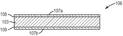
도 2는 본 발명의 적어도 하나의 실시예에 따라 이루어진 다층 전류 컬렉터의 횡단면도이다. 그러한 다층 전류 컬렉터(106)는 기판(103)의 제1표면(108) 상에 건조된 흑연 및 카본블랙 복합층(107a)을 갖추고 기판(103)의 제2표면(109) 상에 건조된 흑연 및 카본블랙 복합층(107b)를 갖춘다.2 is a cross-sectional view of a multilayer current collector made in accordance with at least one embodiment of the present invention. Such a multilayer
더욱이, 개시된 본 발명은 전류 컬렉터 기판의 주면들 모두에 흑연층 및 카본블랙층 및/또는 복합층을 포함하는 다층 전류 컬렉터에 관한 것이다.Moreover, the disclosed invention relates to a multilayer current collector comprising a graphite layer and a carbon black layer and / or a composite layer on all of the major surfaces of the current collector substrate.
여기에 사용된 바와 같이, "복합층"은 카본블랙층 및 흑연층이 결합되거나 혼합되는 영역을 의미하려는 것이다. 상기 복합층은 상기 흑연층과 카본블랙층 사이에 배치될 것이다.As used herein, "composite layer" is intended to mean the area where the carbon black layer and the graphite layer are bonded or mixed. The composite layer will be disposed between the graphite layer and the carbon black layer.
여러 실시예에 있어서, 상기 흑연층은 전류 컬렉터 기판의 어느 한 주면 또는 그 모든 주면 상의 그러한 결합된 층(즉, 흑연, 카본블랙 및 복합층) 전체 두께의 0 내지 99%, 예컨대 10-90%, 20-80%, 30-70%, 또는 40-60%를 포함할 것이다.In some embodiments, the graphite layer is 0 to 99%, such as 10-90%, of the total thickness of such bonded layers (ie, graphite, carbon black and composite layers) on either or all major surfaces of the current collector substrate. , 20-80%, 30-70%, or 40-60%.
여러 실시예에 있어서, 상기 카본블랙층은 전류 컬렉터 기판의 어느 한 주면 또는 그 모든 주면 상의 그러한 결합된 층의 전체 두께의 0 내지 99%, 예컨대 10-90%, 20-80%, 30-70%, 또는 40-60%를 포함할 것이다.In some embodiments, the carbon black layer comprises 0 to 99%, such as 10-90%, 20-80%, 30-70 of the total thickness of such bonded layer on either or all major surfaces of the current collector substrate. %, Or 40-60%.
여러 실시예에 있어서, 흑연과 카본블랙층의 혼합은 거의 없으며, 복합층이 제공되지 않을 수 있다. 다른 실시예들에서는, 복합층이 전류 컬렉터 기판의 어느 한 주면 또는 그 모든 주면 상의 그러한 결합된 층의 전체 두께의 100%까지, 예컨대 10-90%, 20-80%, 30-70%, 또는 40-60%까지 포함되도록 복합층을 형성하기 위해 상기 흑연층 및 카본블랙층의 어느 정도의 혼합이 있을 수 있다.In various embodiments, there is little mixing of the graphite and carbon black layers, and no composite layer may be provided. In other embodiments, the composite layer may be up to 100% of the total thickness of such bonded layer on either or all major surfaces of the current collector substrate, such as 10-90%, 20-80%, 30-70%, or There may be some mixing of the graphite layer and the carbon black layer to form a composite layer to contain up to 40-60%.
복합층이 제공될 때, 흑연층 및 카본블랙층이 유지되는 정도가 개별적으로 서로 다를 것이다. 여러 실시예에 있어서, 흑연층의 일부가 유지되는 반면 흑연층이 제거되어 복합층에서 거의 완전히 없어질 수 있다. 마찬가지로, 여러 실시예에 있어서, 카본블랙층의 일부가 유지되는 반면 카본블랙층이 제거되어 복합층에서 거의 완전히 없어질 수 있다. 여러 실시예에 있어서, 상기 흑연층은 10 내지 40%를 포함하고, 카본블랙층은 10 내지 40%를 포함하며, 복합층은 총 층 두께의 20 내지 80%를 포함할 수 있다.When a composite layer is provided, the extent to which the graphite layer and the carbon black layer are maintained will be individually different. In some embodiments, some of the graphite layer may be retained while the graphite layer may be removed to almost completely disappear from the composite layer. Likewise, in some embodiments, a portion of the carbon black layer may be retained while the carbon black layer may be removed to almost completely disappear from the composite layer. In various embodiments, the graphite layer may comprise 10 to 40%, the carbon black layer may comprise 10 to 40%, and the composite layer may comprise 20 to 80% of the total layer thickness.
더욱이, 본 발명은 울트라캐패시터를 제조하기 위한 방법에 관한 것이며, 상기 방법은 제1포뮬레이션으로부터 전류 컬렉터 기판의 각각의 주면에 걸쳐 제1층을 형성하는 단계, 제2포뮬레이션으로부터 각각의 제1층에 걸쳐 제2층을 형성하는 단계, 및 각각의 제2층에 걸쳐 적어도 하나의 활성 카본층을 형성하는 단계를 포함한다. 실시예들에 있어서, 상기 제1포뮬레이션 및 제2포뮬레이션 중 어느 하나는 흑연 포뮬레이션이고, 상기 제1포뮬레이션 및 제2포뮬레이션 중 또 다른 하나는 카본블랙 포뮬레이션이다.Moreover, the present invention relates to a method for manufacturing an ultracapacitor, the method comprising forming a first layer from a first formulation over each major surface of a current collector substrate, each first from a second formulation. Forming a second layer over the layer, and forming at least one active carbon layer over each second layer. In embodiments, any one of the first and second formulations is a graphite formulation and another one of the first and second formulations is a carbon black formulation.
상기의 개시에 따르면, 제1층 및 제2층이 한정하진 않지만 슬롯 다이 코팅, 슬라이드 비드, 및 커튼 코닝과 같은 기술들을 이용하여 형성될 것이다. 여러 실시예에 있어서, 상기 제1층 및 제2층은 동일한 또는 다른 기술들을 이용하여 형성될 수 있다. 적어도 하나의 실시예에 있어서, 상기 제1층 및 제2층은 슬롯 다이 코팅 기술을 이용하여 형성될 수 있다. 여러 실시예에 있어서, 상기 제1 및 제2층은 동시에 또는 분리적으로 형성, 즉 제1층이 형성된 후 제2층이 형성되거나, 또는 거의 동시에 형성될 수 있다.According to the disclosure above, the first and second layers will be formed using techniques such as, but not limited to, slot die coating, slide beads, and curtain corning. In various embodiments, the first layer and the second layer may be formed using the same or different techniques. In at least one embodiment, the first and second layers can be formed using slot die coating techniques. In various embodiments, the first and second layers may be formed simultaneously or separately, i.e., after the first layer is formed, the second layer is formed, or may be formed at about the same time.
적어도 하나의 실시예에 있어서, 제1 및 제2층은 슬롯 다이, 예컨대 이중 슬롯 다이를 이용하여 거의 동시에 형성될 수 있다. 그와 같은 실시예에 있어서, 상기 2개의 층들은 슬롯에서 합쳐진 후 전류 컬렉터 기판 상에 함께 제공된다. 선택적으로, 2개의 층들은 전류 컬렉터 기판에 적용될 때 공통 비드로 분리적으로 슬롯 다이로부터 빠져나올 수 있다. In at least one embodiment, the first and second layers can be formed almost simultaneously using slot dies, such as dual slot dies. In such an embodiment, the two layers are joined together on a current collector substrate after being joined in a slot. Optionally, the two layers may exit the slot die separately with common beads when applied to the current collector substrate.
원하는 특성의 층(들)을 달성하기 위해, 통상의 기술자의 능력 범위 내에서 예컨대 적절한 코팅 속도, 층 포뮬레이션(들)의 유동률, 심 두께(shim thickness), 건조 조건들, 및 코팅 다이 립과 코팅 표면의 갭 거리와 같은 상기 기판에 제1 및 제2층을 형성하기 위한 파라미터들을 선택할 수 있다.In order to achieve the layer (s) of the desired properties, within the capabilities of one of ordinary skill in the art, for example, a suitable coating speed, flow rate of layer formulation (s), shim thickness, drying conditions, and coating die lip Parameters for forming the first and second layers on the substrate, such as the gap distance of the coating surface, can be selected.
여러 예시의 실시예들에 있어서, 제1층은 전류 컬렉터 기판과 직접 접촉하여 형성될 것이다. 다른 예시의 실시예들에 있어서, 제2층은 상기 제1층과 직접 접촉하여 형성될 것이다. 단지 예시의 방식으로, 일 실시예에서 상기 제1층은 전류 컬렉터 기판과 직접 접촉하는 흑연층이 되고, 상기 제2층은 상기 제1층과 직접 접촉하는 카본블랙층이 될 것이다.In various exemplary embodiments, the first layer will be formed in direct contact with the current collector substrate. In other exemplary embodiments, the second layer will be formed in direct contact with the first layer. By way of example only, in one embodiment the first layer will be a graphite layer in direct contact with the current collector substrate and the second layer will be a carbon black layer in direct contact with the first layer.
또한, 상술한 바와 같이, 상기 방법은 기판 상에 적어도 하나의 추가 층을 형성하는 단계를 포함한다. 상기 추가 층은 상기 제1층과 제2층간, 또는 제2층에 걸쳐 상기 제1층 앞에 형성될 것이다. 단지 예시의 방식으로, 일 실시예에서 상기 추가 층은 전류 컬렉터 기판과 직접 접촉하여 형성될 것이다.In addition, as described above, the method includes forming at least one additional layer on the substrate. The additional layer will be formed in front of the first layer between the first layer and the second layer, or over the second layer. By way of example only, in one embodiment the additional layer will be formed in direct contact with the current collector substrate.
여러 실시예에 있어서, 추가 층이 여기에 기술한 방법들을 이용하여 형성되고, 제1층 및 제2층 중 어느 하나 또는 그 모두로서 거의 동시에 형성되거나, 또는 상기 제1층 및 제2층 중 어느 하나 또는 그 모두가 순차 형성될 수 있다. 단지 예시의 방식로, 일 실시예에 있어서 상기 추가 층은 제1층 및 제2층, 예컨대 트리플 슬롯 다이와 같은 슬롯 다이로 거의 동시에 형성될 것이다.In various embodiments, additional layers are formed using the methods described herein and are formed substantially simultaneously as either or both of the first and second layers, or any of the first and second layers. One or both may be formed sequentially. By way of example only, in one embodiment the additional layer will be formed almost simultaneously with a slot die such as a first layer and a second layer, such as a triple slot die.
상술한 바와 같이, 상기 건조는 한정하진 않지만 인-라인식 오븐(in-line oven), 적외선(IR), 또는 마이크로파와 같은 방법을 이용하여 행해진다. 상기 제1층 및 제2층은 동일하거나 다른 방법들을 이용하여 건조될 것이다. 단지 예시의 방식으로, 일 실시예에 있어서, 상기 제1 및 제2층들은 인-라인식 오븐을 이용하여 건조될 것이다. 적절한 건조 방법(들) 및 파라메터들을 선택하는 것은 통상의 기술자의 능력 범위 내에 있다. 또한 상술한 바와 같이, 전류 컬렉터 기판의 각각의 주면 상의 제1층 및 제2층이 분리적으로, 함께, 또는 합동으로 건조될 수 있다.As mentioned above, the drying is carried out using a method such as, but not limited to, an in-line oven, infrared (IR), or microwave. The first layer and the second layer may be dried using the same or different methods. By way of example only, in one embodiment, the first and second layers will be dried using an in-line oven. Selecting the appropriate drying method (s) and parameters is within the skill of one of ordinary skill. Also as described above, the first and second layers on each major surface of the current collector substrate can be dried separately, together, or jointly.
적어도 하나의 활성 카본층이 전류 컬렉터의 각 측면 상에 제2층에 걸쳐 형성된다. 여기에 사용된 바와 같이, 상기 용어 "활성 카본층"은 적어도 하나의 활성 카본 물질을 포함하는 활성 카본 포뮬레이션의 층을 의미하려는 것이다. 그러한 활성 카본 포뮬레이션에 유용한 활성 카본 물질은 한정하진 않지만, 아주 작은 구멍이 많은 다공성을 만들고 이에 따라 높은 비표면적(high specific surface area)을 갖도록 처리되는 카본을 포함한다. 예컨대, 활성 카본은 300 내지 2500 m2/g의 범위를 갖는 높은 BET 비표면적에 특징이 있다. 여기에 기술된 활성 카본 포뮬레이션에 유용한 활성 카본 물질은 한정하진 않지만, 일본, 오사카의 쿠라레이 케미칼사(Kuraray Chemical Company Ltd), 캘리포니아, 콤프톤의 카본 액티베이티드 코포레이션(Carbon Activated Corporation), 및 뉴저지, 패터슨의 제너럴 카본 코포레이션(General Carbon Corporation)에 의해 판매되는 카본을 포함한다. 전체 내용이 여기에 참조로 반영되는 공통 소유권이 있는 미국출원 제12/335,044호 및 제61/297,469호에 다른 적절한 활성 카본 물질이 개시되어 있다.At least one activated carbon layer is formed over the second layer on each side of the current collector. As used herein, the term "active carbon layer" is intended to mean a layer of an activated carbon formulation comprising at least one activated carbon material. Useful activated carbon materials for such activated carbon formulations include, but are not limited to, carbon that is treated to produce very small porosity porosity and thus high specific surface area. For example, activated carbon is characterized by a high BET specific surface area in the range of 300 to 2500 m 2 / g. Active carbon materials useful for the activated carbon formulations described herein include, but are not limited to, Kuraray Chemical Company Ltd, Osaka, Japan, Carbon Activated Corporation, Compton, California, and Carbon sold by General Carbon Corporation of Patterson, NJ. Other suitable activated carbon materials are disclosed in commonly assigned US applications 12 / 335,044 and 61 / 297,469, which are incorporated herein by reference in their entirety.
여러 실시예에 있어서, 상기 활성 카본은 0.1 내지 100 wt.%의 활성 카본 포뮬레이션, 예컨대 1 내지 99 wt.%, 또는 85 wt.%와 같은 10 내지 90 wt.%의 활성 카본 포뮬레이션을 포함한다.In some embodiments, the activated carbon comprises from 0.1 to 100 wt.% Of an activated carbon formulation, such as from 10 to 90 wt.% Of an activated carbon formulation, such as from 1 to 99 wt.%, Or 85 wt.%. do.
여러 실시예에 있어서, 상기 활성 카본 포뮬레이션은 여기에 기술한 바와 같이 적어도 하나의 바인더(binder)를더 포함한다. 여기에 사용된 바와 같이, 바인더는 한정하진 않지만 폴리테트라플루오로 에틸렌(PTFE; polytetrafluoroethylene), 폴리비닐리덴 플루오르(PVDF; polyvinylidene fluoride), 폴리비닐피롤리돈(PVP; polyvinylpyrrolidone), 폴리비닐 아세테이트(PVA; polyvinyl acetate), 폴리에틸렌 옥사이드(PEO; polyethylene oxide), 폴리프로필렌, 폴리에틸렌, 폴리우레탄, 폴리아크릴레이트, 및 다른 유기(여전히 화학적으로 그리고 전기화학적으로 불활성) 바인더를 포함한다. 적어도 하나의 실시예에 있어서, 상기 바인더는 PTFE가 될 것이다. 여러 실시예에 있어서, 상기 바인더는 0.01 내지 50 wt.%의 활성 카본 포뮬레이션, 예컨대 0.1 내지 49 wt.%, 또는 10 wt.%와 같은 1 내지 40 wt.%의 활성 카본 포뮬레이션을 포함할 것이다.In various embodiments, the activated carbon formulation further comprises at least one binder as described herein. As used herein, the binders include, but are not limited to, polytetrafluoroethylene (PTFE), polyvinylidene fluoride (PVDF), polyvinylpyrrolidone (PVP; polyvinylpyrrolidone), polyvinyl acetate (PVA) polyvinyl acetate), polyethylene oxide (PEO), polypropylene, polyethylene, polyurethane, polyacrylate, and other organic (still chemically and electrochemically inert) binders. In at least one embodiment, the binder will be PTFE. In some embodiments, the binder may comprise 0.01 to 50 wt.% Activated carbon formulation, such as 1 to 40 wt.% Activated carbon formulation, such as 0.1 to 49 wt.%, Or 10 wt.%. will be.
여러 실시예에 있어서, 상기 활성 카본 포뮬레이션은 예컨대 카본블랙; 금속 나노튜브, 로드, 및 와이어; 카본 나노튜브, 로드, 및 와이어; 그래핀 입자; 흑연(천연 또는 합성); 전도성 나노입자; 및 전도성 폴리머와 같은 적어도 하나의 추가 전도성 강화제를 더 포함한다. 적어도 하나의 실시예에 있어서, 상기 전도성 강화제는 카본블랙을 포함한다. 상기 전도성 강화제는 0.01 내지 50 wt.%의 활성 카본 포뮬레이션, 예컨대 0.1 내지 49 wt.%, 또는 5 wt.%와 같은 1 내지 45 wt.%의 활성 카본 포뮬레이션을 포함할 것이다.In some embodiments, the activated carbon formulation is, for example, carbon black; Metal nanotubes, rods, and wires; Carbon nanotubes, rods, and wires; Graphene particles; Graphite (natural or synthetic); Conductive nanoparticles; And at least one additional conductivity enhancer, such as a conductive polymer. In at least one embodiment, the conductivity enhancer comprises carbon black. The conductivity enhancer will comprise from 0.01 to 50 wt.% Of active carbon formulations, such as from 1 to 45 wt.% Of active carbon formulations, such as from 0.1 to 49 wt.%, Or 5 wt.%.
일단 기판 상에 제공되면, 그 활성 카본층의 두께는 100nm 내지 5mm, 예컨대 0.25㎛ 내지 200㎛ 또는 500nm 내지 150㎛의 범위가 될 것이다. 여러 실시예에 있어서, 활성 카본층은 기판 상에서의 두께가 균등하고, 다른 것들은 두께가 균등하지 않을 것이다.Once provided on the substrate, the thickness of the activated carbon layer will be in the range of 100 nm to 5 mm, such as 0.25 μm to 200 μm or 500 nm to 150 μm. In some embodiments, the activated carbon layer will have an even thickness on the substrate and others will not be equal in thickness.
예컨대, 적층 방법, 그라비어 방법(gravure method), 슬롯 다이 또는 사출 방법, 테이프-캐스팅 방법, 공통 롤러 방법, 프레싱, 또는 그들 조합을 포함하는 활성 카본층을 형성하기 위한 적절한 방법들을 선택하는 것은 통상의 기술자의 능력 범위 내에 있다.For example, selecting appropriate methods for forming an active carbon layer including a lamination method, a gravure method, a slot die or injection method, a tape-casting method, a common roller method, pressing, or a combination thereof is conventional. It is within the skill of the technician.
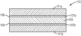
도 3은 본 발명의 적어도 하나의 실시예에 따라 이루어진 울트라캐패시터 전극의 일부를 나타낸 횡단면도이다. 상기 울트라캐패시터 전극(110)은 기판(103)의 제1표면(108) 상에 제1 및 제2층(107a)에 걸친 활성 카본층(111a) 및 기판(103)의 제2표면(109) 상에 제1 및 제2층(107b)에 걸친 활성 카본층(111b)을 갖춘다.3 is a cross-sectional view showing a portion of an ultracapacitor electrode made in accordance with at least one embodiment of the present invention. The
여러 비한정 예시의 실시예들에 있어서, 개시의 방법들은 카본블랙 및 흑연 물질을 포함하는 하나의 포뮬레이션보다 더 안정한 흑연 및 카본블랙층을 형성하기 위한 2개의 포뮬레이션을 이용한다. 따라서, 그러한 개시의 방법들은 여러 배치(batch) 또는 런(run)에 걸쳐 일정한 특성들을 갖는 제품을 신뢰성 있게 만들 수 있다. 또한 여기에 기술된 방법들은 여러 층들에 사용된 포뮬레이션의 구성을 변경함으로써 흑연 및 카본블랙층의 미세구조, 두께, 및 조성을 변경할 수 있게 한다.In several non-limiting example embodiments, the disclosed methods utilize two formulations to form a more stable graphite and carbon black layer than one formulation comprising carbon black and graphite material. Thus, the methods of such disclosure can reliably produce a product having certain characteristics over multiple batches or runs. The methods described herein also allow for changing the microstructure, thickness, and composition of the graphite and carbon black layers by changing the composition of the formulation used in the various layers.
여러 실시예에 있어서, 그러한 개시의 방법들은 현재 기술분야에서 공지된 방법들에 의해 얻어진 제품과 비교하여, 활성 카본층과 전류 컬렉터 기판간 계면 저항을 유지하거나 감소시키는 다층 전류 컬렉터 및/또는 울트라 캐패시터 전극을 제조할 수 있다. 다른 실시예들에 있어서, 상기 방법들은 현재 기술분야에서 공지된 방법에 의해 얻어진 제품과 비교하여, 동일하거나 또는 더 열적으로 강한 다층 전류 컬렉터 및/또는 울트라캐패시터 전극을 제조할 수 있다.In some embodiments, the methods of such disclosure are multilayer current collectors and / or ultracapacitors that maintain or reduce the interface resistance between the active carbon layer and the current collector substrate as compared to products obtained by methods known in the art. Electrodes can be prepared. In other embodiments, the methods may produce the same or more thermally strong multilayer current collectors and / or ultracapacitor electrodes as compared to products obtained by methods known in the art.
여러 실시예에 있어서, 상기 개시의 방법들은 현재 기술분야에서 공지된 방법보다 빠른 속도로 다층 전류 컬렉터 및/또는 울트라 캐패시터 전극을 제조할 수 있다.In various embodiments, the methods of this disclosure can produce multilayer current collectors and / or ultracapacitor electrodes at a faster rate than methods known in the art.
달리 나타내지 않는 한, 본 명세서 및 청구항들에 사용된 모든 숫자는 그렇게 나타내었다 해도 모든 경우 용어 "약"으로 변경되는 것으로 이해해야 한다. 본 명세서 및 청구항들에 사용된 정확한 수치들은 본 발명의 추가 실시예들을 형성한다는 것을 이해해야 한다. 그러한 예에서 개시된 수치들의 정확성을 보장하기 위한 노력들이 이루어진다. 그러나, 소정의 측정된 수치는 본질적으로 각각의 측정 기술에서 발견된 표준편차를 야기하는 소정의 오류를 포함할 수 있다.Unless otherwise indicated, all numbers used in the specification and claims are to be understood as being modified in all instances with the term "about" even if so indicated. It is to be understood that the exact numerical values used in the specification and claims form further embodiments of the invention. Efforts are made to ensure the accuracy of the figures disclosed in such an example. However, certain measured values may inherently contain certain errors that result in the standard deviation found in each measurement technique.
예Yes
이하의 예들은 청구된 바와 같은 발명들로 한정하려는 것은 아니다.The following examples are not intended to be limited to the inventions as claimed.
비교예Comparative Example
1 밀리리터 두께의 알루미늄 포일(세정 또는 처리되지 않은)이 전류 컬렉터 기판으로서 선택된다. 전도성 카본 중간 코팅 잉크가 헨켈(Henkel)의 코팅 잉크 DAG EB 012를 1:1 비율의 탈이온수와 5분동안 핸드 믹싱하여 딥 코팅(dip coating) 적용을 위해 준비되고 2시간 내에 사용한다. 다음에, 기판이 전도성 카본 중간 코팅 잉크로 딥 코팅되도록 기판의 양측면이 동시에 코팅된다. 전도성 중간 코팅의 두께는 1 내지 3μ 범위를 목표로 한다. 다음에, 그러한 코팅된 기판은 적어도 10분 동안 컨벤션 오븐(convection oven)에서 105℃로 베이크(bake)된다.One milliliter thick aluminum foil (cleaned or untreated) is selected as the current collector substrate. A conductive carbon intermediate coating ink is prepared for dip coating application by hand mixing Henkel's coating ink DAG EB 012 with deionized water in a 1: 1 ratio for 5 minutes and used within 2 hours. Next, both sides of the substrate are simultaneously coated so that the substrate is dip coated with a conductive carbon intermediate coating ink. The thickness of the conductive intermediate coating is targeted to the range of 1 to 3 microns. Such coated substrates are then baked at 105 ° C. in a convention oven for at least 10 minutes.
다음에, 그렇게 제조된 전류 컬렉터는 활성 카본 시트의 양측면에 200℃ 및 250 pli(pounds per linear inch)로 적층된다. 상기 활성 카본 시트는 일본 오사카의 쿠라레이 케미칼사의 Kuraray YP50F의 활성 카본을 매사추세츠, 보스톤의 카봇 코포레이션에 의한 BLACK PERALS®2000의 카본블랙과 85:5의 비율로 혼합함으로써 준비된다. 다음에, 델라웨어, 윌밍턴의 DuPont에 의한 Teflon®PTFE613A가 85:5:10 비율의 활성 카본:카본블랙:PTFE를 만들기 위해 추가된다. 이소프로필 알콜이 그 혼합물에 추가되어 혼합된 후 반건조된다. 다음에, 그 재료가 약 9 내지 10 밀리리터 두께의 프리-폼(pre-form)으로 프레스된다. 상기 프리-폼은 체계적인 캘린더링(calendering)에 의해 3 내지 5 밀리리터의 카본 시트로 치밀화된다.The current collector thus produced is then laminated on both sides of the activated carbon sheet at 200 ° C. and 250 pounds per linear inch. The activated carbon sheet is prepared by mixing activated carbon of Kuraray YP50F manufactured by Kuraray Chemical Co., Osaka, Japan, at a ratio of 85: 5 with carbon black of BLACK PERALS ® 2000 by Cabot Corporation of Boston, Massachusetts. Next, Delaware, Teflon ® PTFE613A by DuPont of Wilmington, 85: 5: is added to make the PTFE: activated carbon 10 ratios of carbon black. Isopropyl alcohol is added to the mixture, mixed and semi-dried. The material is then pressed into a pre-form about 9 to 10 milliliters thick. The pre-form is densified to 3-5 milliliters of carbon sheet by systematic calendering.
결과의 형성된 전극의 평면 영역에 걸친 비저항은 13/16인치 직경의 디스크를 펀칭(punching)하여 평면 영역에 걸친 비저항(수신한 바와 같은)을 측정함으로써 얻어진다. 각 실린더 상부를 커버하는 실버 포일 콘택트를 갖는 2개의 세라믹 실린더(직경=1인치) 사이의 그러한 샘플 상에 1001b 로드(load)를 인가하기 위해 Instron 4202가 사용된다. 키슬리 멀티미터(Keithley multimeter) 2700을 이용하여 DC 4선 저항 측정이 이루어지고, 이후 비저항에 대한 저항치가 계산된다.The resistivity over the planar region of the resulting formed electrode is obtained by punching a 13/16 inch diameter disk to measure the resistivity (as received) over the planar region. Instron 4202 is used to apply a 1001b load on such a sample between two ceramic cylinders (diameter = 1 inch) with silver foil contacts covering each cylinder top. DC 4-wire resistance measurements are made using a Keithley multimeter 2700, and then the resistance to resistivity is calculated.
다음에, 상기 샘플이 적어도 16시간 동안 150℃에서 가열되고, 식힌 후, 다시 평면 영역에 걸친 비저항을 측정한다.The sample is then heated at 150 ° C. for at least 16 hours, cooled, and then measured for resistivity again over the planar region.
그러한 전극 샘플은 16시간 동안 150℃ 노출 후 0.10 ohm-cm2(수신한 바와 같은)와 0.11 ohm-cm2의 측정된 평면 영역에 걸친 비저항을 나타냈다. 따라서, 전도성 카본 중간 코팅은 양호한 특성 및 열적 안정성을 나타냈다.Such electrode samples exhibited resistivity over the measured planar regions of 0.10 ohm-cm 2 (as received) and 0.11 ohm-cm 2 after 150 ° C. exposure for 16 hours. Thus, the conductive carbon intermediate coating exhibited good properties and thermal stability.
발명예Honor
제1층 포뮬레이션(흑연 포뮬레이션)은 뉴저지, 애즈버리의 애즈버리 카본사의 GK572를 이용하여 준비한다. 50:50의 GK572:탈이온수 희석은 약 5분 동안 혼합하여 준비한다. 그 혼합물은 안정한 분산재를 유지했다.The first layer formulation (graphite formulation) is prepared using GK572 of Asbury Carbon, Asbury, NJ. A 50:50 GK572: deionized water dilution is prepared by mixing for about 5 minutes. The mixture maintained a stable dispersion.
제2층 포뮬레이션(카본블랙 포뮬레이션)은 헨켈(Henkel)의 DAG EB 012를 이용하여 준비한다. 60:40의 DAG:탈이온수 희석은 약 5분 동안 혼합한 후 그 혼합물을 3일 동안 가라앉혀 준비한다. 가라앉힌지 3일째에 그 부유액을 채취한다.The second layer formulation (carbon black formulation) is prepared using Henkel's DAG EB 012. A 60:40 DAG: deionized water dilution is prepared by mixing for about 5 minutes and then allowing the mixture to settle for 3 days. The suspension is collected three days after sinking.
1밀리미터 두께 알루미늄 포일(세정 또는 처리하지 않은)이 전류 컬렉터 기판으로 선택되어 제1 및 제2층 포뮬레이션을 이용하여 슬롯 다이 코팅된다. 우선, 그 기판의 한측면이 다층 슬롯 다이를 이용하여 22 ft/min 선 속도로 코팅된다. 3밀리미터의 두꺼운 심(shim)을 이용한 제1포뮬레이션 유동률은 1.3 ml/min이였다. 5밀리미터의 두꺼운 심을 이용한 제2포뮬레이션 유동률은 4.8 ml/min이였다. 다음에, 그 코팅된 기판은 239℉에서 인-라인식 오븐을 통해 건조했다.A 1 millimeter thick aluminum foil (clean or untreated) is chosen as the current collector substrate and slot die coated using the first and second layer formulations. First, one side of the substrate is coated at a 22 ft / min line speed using a multilayer slot die. The first formulation flow rate using a 3 mm thick shim was 1.3 ml / min. The second formulation flow rate using a 5 mm thick shim was 4.8 ml / min. The coated substrate was then dried through an in-line oven at 239 ° F.
다음에, 상기 기판의 또 다른 표면은 상기 동일한 조건 하에 다층 슬롯-다이로 코팅되고, 239℉에서 인-라인 건조했다.Next, another surface of the substrate was coated with a multilayer slot-die under the same conditions and dried in-line at 239 ° F.
다음에, 제조된 전류 컬렉터는 상기 비교예에서 기술한 바와 같이 활성 카본 시트의 양측면에 적층된다.Next, the manufactured current collector is laminated on both sides of the activated carbon sheet as described in the comparative example.
상술한 방법을 이용하여, 그러한 결과의 형성된 전극 샘플은 16시간 동안 150℃ 노출 후 0.11 ohm-cm2(수신한 바와 같은)와 0.11 ohm-cm2의 측정된 평면 영역에 걸친 비저항을 나타냈다.Using the method described above, the resulting electrode sample exhibited a resistivity over the measured planar regions of 0.11 ohm-cm 2 (as received) and 0.11 ohm-cm 2 after 150 ° C. exposure for 16 hours.
이러한 데이터는 비교예 1의 제품과 같은 유사한 전도성 중간 코팅 특성을 암시한다. 그러나, 상기 발명예의 방법은 좀더 콘트롤된 다용도의 방법이다. 예컨대, 상기한 비교예의 잉크는 단지 약 2시간의 작업 수명을 갖는 반면, 상기한 발명예의 2개의 포뮬레이션은 안정적이다.These data suggest similar conductive intermediate coating properties as the product of Comparative Example 1. However, the inventive method is a more controlled and versatile method. For example, the ink of the above comparative example has a working life of only about 2 hours, while the two formulations of the above-described invention are stable.
Claims (23)
제2포뮬레이션으로부터 각각의 제1층에 걸쳐 제2층을 형성하는 단계를 포함하며,
상기 제1포뮬레이션 및 제2포뮬레이션 중 어느 하나는 흑연 포뮬레이션이고, 상기 제1포뮬레이션 및 제2포뮬레이션 중 또 다른 하나는 카본블랙 포뮬레이션인 것을 특징으로 하는 다층 전류 컬렉터를 제조하기 위한 방법.Forming a first layer over each major surface of the current collector substrate from the first formulation; And
Forming a second layer over each first layer from the second formulation,
Any one of the first and second formulations is a graphite formulation, and another one of the first and second formulations is a carbon black formulation. Way.
적어도 하나의 제1층은 전류 컬렉터 기판의 주면과 직접 접촉하는 것을 특징으로 하는 다층 전류 컬렉터를 제조하기 위한 방법.The method according to claim 1,
At least one first layer is in direct contact with the major surface of the current collector substrate.
적어도 하나의 제1층은 전류 컬렉터 기판의 주면과 직접 접촉하고 각각의 제2층은 제1층과 직접 접촉하는 것을 특징으로 하는 다층 전류 컬렉터를 제조하기 위한 방법.The method according to claim 1,
At least one first layer is in direct contact with the major surface of the current collector substrate and each second layer is in direct contact with the first layer.
각각의 제1층에 걸쳐 제2층을 형성하기 전에 각각의 제1층을 건조하는 단계를 더 포함하는 것을 특징으로 하는 다층 전류 컬렉터를 제조하기 위한 방법.The method according to claim 1,
And drying each first layer prior to forming a second layer over each first layer.
전류 컬렉터 기판의 또 다른 주면 상에 제1층 및 제2층을 형성하기 전에 전류 컬렉터 기판의 어느 한 주면 상의 제1층 및 제2층을 건조시키는 단계를 더 포함하는 것을 특징으로 하는 다층 전류 컬렉터를 제조하기 위한 방법.The method according to claim 1,
And drying the first and second layers on either major surface of the current collector substrate prior to forming the first and second layers on another major surface of the current collector substrate. Method for preparing the same.
상기 제1층은 흑연층인 것을 특징으로 하는 다층 전류 컬렉터를 제조하기 위한 방법.The method according to claim 1,
Wherein said first layer is a graphite layer.
카본블랙층은 0.005㎛ 내지 0.1㎛ 범위의 평균 입자 직경 및 1㎛ 내지 100㎛ 범위의 평균 덩어리 직경을 갖는 적어도 하나의 카본블랙 물질로 이루어진 것을 특징으로 하는 다층 전류 컬렉터를 제조하기 위한 방법.The method according to claim 1,
Wherein the carbon black layer is comprised of at least one carbon black material having an average particle diameter in the range of 0.005 μm to 0.1 μm and an average agglomerate diameter in the range of 1 μm to 100 μm.
흑연층은 0.1㎛ 내지 100㎛ 범위의 평균 입자 직경을 갖는 적어도 하나의 흑연 물질을 포함하는 것을 특징으로 하는 다층 전류 컬렉터를 제조하기 위한 방법.The method according to claim 1,
The graphite layer comprises at least one graphite material having an average particle diameter in the range of 0.1 μm to 100 μm.
상기 형성 단계동안 흑연 포뮬레이션은 300 cps 이하의 점성을 갖는 것을 특징으로 하는 다층 전류 컬렉터를 제조하기 위한 방법.The method according to claim 1,
Wherein said graphite formulation has a viscosity of 300 cps or less during said forming step.
제1포뮬레이션 및 제2포뮬레이션 중 적어도 어느 하나는 적어도 하나의 전도성 강화제를 더 포함하는 것을 특징으로 하는 다층 전류 컬렉터를 제조하기 위한 방법.The method according to claim 1,
At least one of the first formulation and the second formulation further comprises at least one conductivity enhancer.
적어도 하나의 추가 층을 형성하는 단계를 더 포함하는 것을 특징으로 하는 다층 전류 컬렉터를 제조하기 위한 방법.The method according to claim 1,
Further comprising forming at least one additional layer.
적어도 하나의 추가 층을 형성하는 단계를 더 포함하며, 상기 적어도 하나의 추가 층은 적어도 하나의 전도성 강화제를 포함하는 것을 특징으로 하는 다층 전류 컬렉터를 제조하기 위한 방법.The method according to claim 1,
Forming at least one additional layer, the at least one additional layer comprising at least one conductivity enhancer.
전류 컬렉터 기판의 적어도 한 주면과 직접 접촉하는 적어도 하나의 추가 층을 형성하는 단계를 더 포함하는 것을 특징으로 하는 다층 전류 컬렉터를 제조하기 위한 방법.The method according to claim 1,
Forming at least one additional layer in direct contact with at least one major surface of the current collector substrate.
전류 컬렉터 기판의 적어도 한 주면과 직접 접촉하는 적어도 하나의 추가 층을 형성하는 단계를 더 포함하며, 상기 적어도 하나의 추가 층은 물을 포함하는 것을 특징으로 하는 다층 전류 컬렉터를 제조하기 위한 방법.The method according to claim 1,
Forming at least one additional layer in direct contact with at least one major surface of the current collector substrate, wherein the at least one additional layer comprises water.
상기 제1층 및 제2층은 거의 동시에 형성되는 것을 특징으로 하는 다층 전류 컬렉터를 제조하기 위한 방법.The method according to claim 1,
Wherein said first layer and said second layer are formed at about the same time.
상기 제1층 및 제2층은 슬롯-다이를 이용하여 거의 동시에 형성되는 것을 특징으로 하는 다층 전류 컬렉터를 제조하기 위한 방법.The method according to claim 1,
Wherein said first layer and said second layer are formed at about the same time using a slot-die.
제2포뮬레이션으로부터 각각의 제1층에 걸쳐 제2층을 형성하는 단계; 및
각각의 제2층에 걸쳐 적어도 하나의 활성 카본층을 형성하는 단계를 포함하며,
상기 제1포뮬레이션 및 제2포뮬레이션 중 어느 하나는 흑연 포뮬레이션이고, 상기 제1포뮬레이션 및 제2포뮬레이션 중 또 다른 하나는 카본블랙 포뮬레이션인 것을 특징으로 하는 울트라캐패시터 전극을 제조하기 위한 방법.Forming a first layer over each major surface of the current collector substrate from the first formulation;
Forming a second layer over each first layer from the second formulation; And
Forming at least one activated carbon layer over each second layer,
Any one of the first and second formulations is a graphite formulation, and another one of the first and second formulations is a carbon black formulation. Way.
상기 제1층은 흑연층인 것을 특징으로 하는 울트라캐패시터 전극을 제조하기 위한 방법.The method of claim 19,
And said first layer is a graphite layer.
상기 제1층 및 제2층은 슬롯-다이를 이용하여 거의 동시에 형성되는 것을 특징으로 하는 울트라캐패시터 전극을 제조하기 위한 방법.The method of claim 19,
Wherein said first and second layers are formed at about the same time using slot-dies.
전류 컬렉터 기판의 또 다른 주면 상에 제1층 및 제2층을 형성하기 전에 전류 컬렉터 기판의 어느 한 주면 상의 제1층 및 제2층을 건조시키는 단계를 더 포함하는 것을 특징으로 하는 울트라캐패시터 전극을 제조하기 위한 방법.The method of claim 19,
Ultracapacitor electrode further comprising drying the first and second layers on either major surface of the current collector substrate before forming the first and second layers on another major surface of the current collector substrate. Method for preparing the same.
상기 전류 컬렉터 기판의 각각의 주면에 걸쳐 형성된 복합층을 포함하며,
상기 복합층은 흑연 및 카본블랙을 포함하고, 상기 복합층에서의 총 고체에 대한 흑연의 비율은 약 2 내지 50 vol%인 것을 특징으로 하는 다층 전류 컬렉터.A current collector substrate, and
A composite layer formed over each major surface of the current collector substrate,
Wherein the composite layer comprises graphite and carbon black, and the ratio of graphite to total solids in the composite layer is about 2 to 50 vol%.
Applications Claiming Priority (3)
| Application Number | Priority Date | Filing Date | Title |
|---|---|---|---|
| US12/860,995 US8840687B2 (en) | 2010-08-23 | 2010-08-23 | Dual-layer method of fabricating ultracapacitor current collectors |
| US12/860,995 | 2010-08-23 | ||
| PCT/US2011/047173 WO2012027102A1 (en) | 2010-08-23 | 2011-08-10 | Dual-layer method of fabricating ultracapacitor current collectors |
Publications (1)
| Publication Number | Publication Date |
|---|---|
| KR20130139882A true KR20130139882A (en) | 2013-12-23 |
Family
ID=44511579
Family Applications (1)
| Application Number | Title | Priority Date | Filing Date |
|---|---|---|---|
| KR1020137007383A KR20130139882A (en) | 2010-08-23 | 2011-08-10 | Dual-layer method of fabricating ultracapacitor current collectors |
Country Status (7)
| Country | Link |
|---|---|
| US (1) | US8840687B2 (en) |
| EP (1) | EP2609605A1 (en) |
| JP (2) | JP2013536591A (en) |
| KR (1) | KR20130139882A (en) |
| CN (1) | CN103098161B (en) |
| TW (1) | TW201232582A (en) |
| WO (1) | WO2012027102A1 (en) |
Families Citing this family (6)
| Publication number | Priority date | Publication date | Assignee | Title |
|---|---|---|---|---|
| EP2835851A4 (en) * | 2012-04-04 | 2016-03-09 | Uacj Corp | Collector, electrode structure, nonaqueous electrolyte battery, and electricity storage component |
| US9478364B2 (en) * | 2013-08-22 | 2016-10-25 | Corning Incorporated | Carbon-based electrodes containing molecular sieve |
| CN106602076B (en) * | 2017-01-06 | 2019-02-26 | 中航锂电(洛阳)有限公司 | Carbon-coated aluminum foils, preparation method and application |
| US11017958B2 (en) | 2017-02-07 | 2021-05-25 | Massachusetts Institute Of Technology | Monolithic flexible supercapacitors, methods of making and uses thereof |
| FR3076062B1 (en) * | 2017-12-21 | 2020-07-17 | Commissariat A L'energie Atomique Et Aux Energies Alternatives | REALIZATION OF A MICROELECTRONIC DEVICE COLLECTOR |
| US20220096981A1 (en) * | 2018-11-29 | 2022-03-31 | Cabot Corporation | Pelletized activated carbon and methods of production |
Family Cites Families (51)
| Publication number | Priority date | Publication date | Assignee | Title |
|---|---|---|---|---|
| IT557307A (en) | 1955-02-23 | 1900-01-01 | ||
| GB1048829A (en) * | 1963-12-10 | 1966-11-23 | Ilford Ltd | High speed coating apparatus |
| US4001024A (en) | 1976-03-22 | 1977-01-04 | Eastman Kodak Company | Method of multi-layer coating |
| JPH05299297A (en) * | 1992-04-17 | 1993-11-12 | Osaka Gas Co Ltd | Electrical double-layer capacitor |
| US5286415A (en) | 1992-12-28 | 1994-02-15 | Advanced Products, Inc. | Water-based polymer thick film conductive ink |
| US5478676A (en) | 1994-08-02 | 1995-12-26 | Rexam Graphics | Current collector having a conductive primer layer |
| JP3417119B2 (en) * | 1995-02-08 | 2003-06-16 | 松下電器産業株式会社 | Electric double layer capacitor |
| US5849371A (en) | 1996-07-22 | 1998-12-15 | Beesley; Dwayne | Laser and laser-assisted free electron beam deposition apparatus and method |
| JP3719570B2 (en) | 1997-10-20 | 2005-11-24 | 株式会社パワーシステム | Electric double layer capacitor |
| US6493210B2 (en) | 1998-01-23 | 2002-12-10 | Matsushita Electric Industrial Co., Ltd. | Electrode metal material, capacitor and battery formed of the material and method of producing the material and the capacitor and battery |
| US6310762B1 (en) | 1998-03-03 | 2001-10-30 | Jeol Ltd. | Carbon material for electric double layer capacitor, method of producing same, electric double layer capacitor and method of fabricating same |
| JP2000077273A (en) | 1998-09-03 | 2000-03-14 | Ngk Insulators Ltd | Electric double-layered capacitor and manufacture thereof |
| US6304426B1 (en) | 1998-09-29 | 2001-10-16 | General Electric Company | Method of making an ultracapacitor electrode |
| US6201685B1 (en) | 1998-10-05 | 2001-03-13 | General Electric Company | Ultracapacitor current collector |
| US6072692A (en) | 1998-10-08 | 2000-06-06 | Asahi Glass Company, Ltd. | Electric double layer capacitor having an electrode bonded to a current collector via a carbon type conductive adhesive layer |
| JP2000277393A (en) * | 1999-03-24 | 2000-10-06 | Ngk Insulators Ltd | Electric double-layer capacitor and its manufacturing method |
| US6358650B2 (en) | 1999-07-28 | 2002-03-19 | Mitsubishi Chemical Corporation | Current collector having a uniformly applied lithium polysilicate primer and associated fabrication process |
| US6426863B1 (en) * | 1999-11-25 | 2002-07-30 | Lithium Power Technologies, Inc. | Electrochemical capacitor |
| US6403263B1 (en) | 2000-09-20 | 2002-06-11 | Moltech Corporation | Cathode current collector for electrochemical cells |
| JP2002270470A (en) * | 2001-03-09 | 2002-09-20 | Osaka Gas Co Ltd | Electric double-layered capacitor |
| US6714391B2 (en) | 2001-10-04 | 2004-03-30 | Ise Research Corporation | Ultracapacitor energy storage cell pack and methods of assembling and cooling the same |
| AUPR977301A0 (en) | 2001-12-28 | 2002-01-31 | Energy Storage Systems Pty Ltd | An electrode for an energy storage device |
| US7195834B2 (en) * | 2002-05-23 | 2007-03-27 | Columbian Chemicals Company | Metallized conducting polymer-grafted carbon material and method for making |
| ATE354856T1 (en) * | 2002-05-23 | 2007-03-15 | Columbian Chem | SULFONATED CONDUIT GRAFT POLYMER CARBON MATERIAL FOR FUEL CELL APPLICATIONS |
| US7459103B2 (en) * | 2002-05-23 | 2008-12-02 | Columbian Chemicals Company | Conducting polymer-grafted carbon material for fuel cell applications |
| CN1310354C (en) * | 2002-06-04 | 2007-04-11 | 伊藤忠商事株式会社 | Conductive material-mixed electrode active material, electrode structure, secondary cell, amd method for producing conductive material-mixed electrode active material |
| EP1516377A2 (en) * | 2002-06-05 | 2005-03-23 | Reveo, Inc. | Layered electrochemical cell and manufacturing method therefor |
| US6917094B2 (en) | 2002-11-29 | 2005-07-12 | Honda Motor Co., Ltd | Electrode for electric double layer capacitor |
| US7508651B2 (en) | 2003-07-09 | 2009-03-24 | Maxwell Technologies, Inc. | Dry particle based adhesive and dry film and methods of making same |
| US20050266298A1 (en) | 2003-07-09 | 2005-12-01 | Maxwell Technologies, Inc. | Dry particle based electro-chemical device and methods of making same |
| US20110165318A9 (en) | 2004-04-02 | 2011-07-07 | Maxwell Technologies, Inc. | Electrode formation by lamination of particles onto a current collector |
| US7352558B2 (en) | 2003-07-09 | 2008-04-01 | Maxwell Technologies, Inc. | Dry particle based capacitor and methods of making same |
| US7495349B2 (en) | 2003-10-20 | 2009-02-24 | Maxwell Technologies, Inc. | Self aligning electrode |
| JP4916720B2 (en) | 2004-01-19 | 2012-04-18 | パナソニック株式会社 | ELECTRIC DOUBLE LAYER CAPACITOR, ITS MANUFACTURING METHOD, AND ELECTRONIC DEVICE USING THE SAME |
| US7090946B2 (en) * | 2004-02-19 | 2006-08-15 | Maxwell Technologies, Inc. | Composite electrode and method for fabricating same |
| WO2005112057A1 (en) | 2004-05-13 | 2005-11-24 | Matsushita Electric Industrial Co., Ltd. | Electric double-layer capacitor and production method therefor |
| JP2006210883A (en) * | 2004-12-27 | 2006-08-10 | Matsushita Electric Ind Co Ltd | Polarizable electrode, its manufacturing method and electrochemical capacitor using the same |
| JPWO2006070617A1 (en) | 2004-12-27 | 2008-06-12 | 松下電器産業株式会社 | Polarized electrode body, method for producing the same, and electrochemical capacitor using the same |
| UA90448C2 (en) | 2005-06-25 | 2010-05-11 | Юрій Андрійович Малєтін | Method for manufacturing electrodes with a low contact resistance for batteries and capacitors with a double electric layer |
| JP2008034215A (en) * | 2006-07-28 | 2008-02-14 | Hitachi Ltd | Lithium secondary battery, positive electrode therefor, and its manufacturing method |
| US7881042B2 (en) * | 2006-10-26 | 2011-02-01 | Axion Power International, Inc. | Cell assembly for an energy storage device with activated carbon electrodes |
| US20080151472A1 (en) | 2006-12-20 | 2008-06-26 | Maletin Yuriy A | Electrochemical double layer capacitor |
| US8472163B2 (en) * | 2007-02-19 | 2013-06-25 | Universal Supercapacitors Llc | Negative electrode current collector for heterogeneous electrochemical capacitor and method of manufacture thereof |
| US9056449B2 (en) | 2007-10-01 | 2015-06-16 | Intelligent Energy Limited | Methods of manufacturing electrochemical cells |
| CN102007627B (en) * | 2008-04-18 | 2014-04-09 | 株式会社丰田自动织机 | Negative electrode for lithium ion secondary battery, and method for production thereof |
| US8411413B2 (en) | 2008-08-28 | 2013-04-02 | Ioxus, Inc. | High voltage EDLC cell and method for the manufacture thereof |
| JP2009277783A (en) * | 2008-05-13 | 2009-11-26 | Japan Gore Tex Inc | Conductive adhesive, electrode for electric double layer capacitor using the same, and electric double layer capacitor |
| JP5470780B2 (en) * | 2008-09-03 | 2014-04-16 | 東洋インキScホールディングス株式会社 | Battery composition |
| JP2010097830A (en) * | 2008-10-16 | 2010-04-30 | Nippon Zeon Co Ltd | Manufacturing method of electrode for electrochemical element |
| US8318356B2 (en) | 2008-12-15 | 2012-11-27 | Corning Incorporated | Activated carbon materials for high energy density ultracapacitors |
| KR20120027364A (en) * | 2009-05-26 | 2012-03-21 | 옵토도트 코포레이션 | Lithium batteries utilizing nanoporous separator layers |
-
2010
- 2010-08-23 US US12/860,995 patent/US8840687B2/en not_active Expired - Fee Related
-
2011
- 2011-08-10 JP JP2013525939A patent/JP2013536591A/en active Pending
- 2011-08-10 CN CN201180040814.2A patent/CN103098161B/en not_active Expired - Fee Related
- 2011-08-10 EP EP11748833.8A patent/EP2609605A1/en not_active Withdrawn
- 2011-08-10 WO PCT/US2011/047173 patent/WO2012027102A1/en active Application Filing
- 2011-08-10 TW TW100128466A patent/TW201232582A/en unknown
- 2011-08-10 KR KR1020137007383A patent/KR20130139882A/en not_active Application Discontinuation
-
2016
- 2016-06-17 JP JP2016120558A patent/JP2016201549A/en active Pending
Also Published As
| Publication number | Publication date |
|---|---|
| CN103098161B (en) | 2016-04-13 |
| TW201232582A (en) | 2012-08-01 |
| WO2012027102A1 (en) | 2012-03-01 |
| EP2609605A1 (en) | 2013-07-03 |
| JP2013536591A (en) | 2013-09-19 |
| CN103098161A (en) | 2013-05-08 |
| US8840687B2 (en) | 2014-09-23 |
| US20120043120A1 (en) | 2012-02-23 |
| JP2016201549A (en) | 2016-12-01 |
Similar Documents
| Publication | Publication Date | Title |
|---|---|---|
| Wang et al. | Flexible supercapacitors based on cloth-supported electrodes of conducting polymer nanowire array/SWCNT composites | |
| Zhou et al. | A three-dimensional flexible supercapacitor with enhanced performance based on lightweight, conductive graphene-cotton fabric electrode | |
| TWI601330B (en) | Electrode material and energy storage apparatus | |
| KR20130139882A (en) | Dual-layer method of fabricating ultracapacitor current collectors | |
| US8687346B2 (en) | Multi-layered electrode for ultracapacitors | |
| Lee et al. | A metal-oxide nanofiber-decorated three-dimensional graphene hybrid nanostructured flexible electrode for high-capacity electrochemical capacitors | |
| EP2261934A1 (en) | Ionic liquid-containing electrode membrane and electrode, process for producing the electrode membrane and the electrode, and electric storage device | |
| US20150064571A1 (en) | Current collector structure | |
| Sekhar et al. | Birnessite-type MnO 2 nanosheet arrays with interwoven arrangements on vapor grown carbon fibers as hybrid nanocomposites for pseudocapacitors | |
| Karaca et al. | Galvanostatic synthesis of nanostructured Ag‐Ag2O dispersed PPy composite on graphite electrode for supercapacitor applications | |
| US8002921B2 (en) | Electrodes for electric double layer devices | |
| CN103003901A (en) | Solid electrolytic capacitor | |
| JP2017123471A (en) | Current conducting electrode and method for manufacturing the same | |
| US10981794B1 (en) | Stable aqueous dispersion of carbon | |
| JP6827657B2 (en) | Electrochemical device and its manufacturing method | |
| KR101919048B1 (en) | Manufacturing method of anode for lithium secondary battery | |
| KR102543247B1 (en) | Multiple coated electrode, method for preparing the same, and an energy storage device including the multiple coated electrode | |
| TWI668902B (en) | Electrode and electrochemical energy storage device | |
| KR102239685B1 (en) | Electro-conductive adhesive using activated carbon, electrode current collector, electrode for supercapacitor and the supercapacitor having improved high temperature performance | |
| Dulyaseree et al. | Supercapacitor based on multi-walled carbon nanotubes/carbon black composites-coated wooden sheet | |
| RU2751537C1 (en) | Multichannel electrode | |
| KR102188709B1 (en) | Carbon structure and method of fabricating of the same | |
| WO2022092010A1 (en) | Carbon paste for solid electrolytic capacitors, solid electrolytic capacitor element, and solid electrolytic capacitor | |
| US20210090820A1 (en) | Self-supporting carbon electrode | |
| KR20210045023A (en) | Tin-doped lithium chromium titanium phosphate, method for preparing and electrode comprising the same |
Legal Events
| Date | Code | Title | Description |
|---|---|---|---|
| A201 | Request for examination | ||
| E902 | Notification of reason for refusal | ||
| E601 | Decision to refuse application |