KR20130121020A - Electrostatic chuck - Google Patents
Electrostatic chuck Download PDFInfo
- Publication number
- KR20130121020A KR20130121020A KR1020130041512A KR20130041512A KR20130121020A KR 20130121020 A KR20130121020 A KR 20130121020A KR 1020130041512 A KR1020130041512 A KR 1020130041512A KR 20130041512 A KR20130041512 A KR 20130041512A KR 20130121020 A KR20130121020 A KR 20130121020A
- Authority
- KR
- South Korea
- Prior art keywords
- plate
- suction
- electrostatic chuck
- insulator
- base
- Prior art date
Links
Images


Classifications
-
- H—ELECTRICITY
- H01—ELECTRIC ELEMENTS
- H01L—SEMICONDUCTOR DEVICES NOT COVERED BY CLASS H10
- H01L21/00—Processes or apparatus adapted for the manufacture or treatment of semiconductor or solid state devices or of parts thereof
- H01L21/67—Apparatus specially adapted for handling semiconductor or electric solid state devices during manufacture or treatment thereof; Apparatus specially adapted for handling wafers during manufacture or treatment of semiconductor or electric solid state devices or components ; Apparatus not specifically provided for elsewhere
- H01L21/683—Apparatus specially adapted for handling semiconductor or electric solid state devices during manufacture or treatment thereof; Apparatus specially adapted for handling wafers during manufacture or treatment of semiconductor or electric solid state devices or components ; Apparatus not specifically provided for elsewhere for supporting or gripping
- H01L21/6831—Apparatus specially adapted for handling semiconductor or electric solid state devices during manufacture or treatment thereof; Apparatus specially adapted for handling wafers during manufacture or treatment of semiconductor or electric solid state devices or components ; Apparatus not specifically provided for elsewhere for supporting or gripping using electrostatic chucks
- H01L21/6833—Details of electrostatic chucks
-
- B—PERFORMING OPERATIONS; TRANSPORTING
- B23—MACHINE TOOLS; METAL-WORKING NOT OTHERWISE PROVIDED FOR
- B23Q—DETAILS, COMPONENTS, OR ACCESSORIES FOR MACHINE TOOLS, e.g. ARRANGEMENTS FOR COPYING OR CONTROLLING; MACHINE TOOLS IN GENERAL CHARACTERISED BY THE CONSTRUCTION OF PARTICULAR DETAILS OR COMPONENTS; COMBINATIONS OR ASSOCIATIONS OF METAL-WORKING MACHINES, NOT DIRECTED TO A PARTICULAR RESULT
- B23Q3/00—Devices holding, supporting, or positioning work or tools, of a kind normally removable from the machine
- B23Q3/15—Devices for holding work using magnetic or electric force acting directly on the work
-
- H—ELECTRICITY
- H02—GENERATION; CONVERSION OR DISTRIBUTION OF ELECTRIC POWER
- H02N—ELECTRIC MACHINES NOT OTHERWISE PROVIDED FOR
- H02N13/00—Clutches or holding devices using electrostatic attraction, e.g. using Johnson-Rahbek effect
Abstract
Description
본 발명은 정척 척에 관한 것이다.The present invention relates to a chuck.
IC(integrated circuits) 및 LSI(large scale integration) 회로 등의 반도체 디바이스의 제조 공정에서 이용되는 막 증착 시스템(예를 들면, CVD(chemical vapor deposition) 시스템 및 PVD(physical vapor deposition) 시스템) 및 플라즈마 에칭 시스템 각각에서는, 진공 처리 챔버에서 기판(예를 들면, 실리콘 웨이퍼)을 정밀하게 유지하는 스테이지를 포함한다. 일본국 특개2006-344613호에는, 이러한 스테이지로서 사용되는 정전 척의 예가 기재되어 있다.Film deposition systems (eg, chemical vapor deposition (CVD) and physical vapor deposition (PVD) systems) and plasma etching used in the fabrication of semiconductor devices, such as integrated circuits (ICs) and large scale integration (LSI) circuits. Each system includes a stage for precisely holding a substrate (eg, a silicon wafer) in a vacuum processing chamber. Japanese Patent Laid-Open No. 2006-344613 describes an example of an electrostatic chuck used as such a stage.
이 정전 척은 기판(실리콘 웨이퍼)을 정전기적으로 유지하는 정전 척(electrostatic chuck; ESC) 흡인 플레이트를 포함한다. 정전 척은 온도 제어를 행해서 척에 의해 유지된 기판을 제어 온도에 유지한다. 정전 척은 쿨롱(Coulomb) 정전 척 또는 존슨-라벡(Johnsen-Rahbek) 정전 척일 수 있다. 쿨롱 정전 척은 인가 전압에 매우 민감한 흡인력을 발생시킨다. 그러나, 쿨롱 정전 척은 고전압의 인가를 요한다. 또한, 쿨롱 정전 척은, ESC 흡인 플레이트와 기판 사이에 접촉 에어리어가 작을 경우 충분한 흡인력을 발생시킬 수 없다. 존슨-라벡 정전 척은, ESC 흡인 플레이트와 기판 사이에 접촉 에어리어가 작을 경우에도 충분한 흡인력을 발생시킨다. 그러나, 존슨-라벡 정전 척은 기판에 공급될 전류를 요한다.The electrostatic chuck includes an electrostatic chuck (ESC) suction plate that electrostatically holds the substrate (silicon wafer). The electrostatic chuck performs temperature control to maintain the substrate held by the chuck at the control temperature. The electrostatic chuck can be a Coulomb electrostatic chuck or a Johnson-Rahbek electrostatic chuck. The coulomb electrostatic chuck generates a suction force which is very sensitive to the applied voltage. However, Coulomb electrostatic chucks require the application of high voltages. In addition, the coulomb electrostatic chuck cannot generate sufficient suction force when the contact area between the ESC suction plate and the substrate is small. The Johnson-Lavec electrostatic chuck generates sufficient suction force even when the contact area between the ESC suction plate and the substrate is small. However, Johnson-Labeck electrostatic chucks require current to be supplied to the substrate.
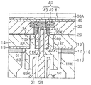
도 7은 정전 척(80)의 종례 예를 나타내는 단면도이다. 정전 척(80)은 베이스(81) 및 점착층(82)에 의해 베이스(81)에 본딩된 ESC 흡인 플레이트(83)를 포함한다. 베이스(81)는, 예를 들면 알루미늄으로 형성될 수 있다. 점착층(82)은, 예를 들면 실리콘 수지로 형성될 수 있다.7 is a cross-sectional view illustrating an example of the
베이스(81)는 ESC 흡인 플레이트(83)를 지지한다. 베이스(81)는 히터(84)를 내장한다. 전압의 공급 시 열을 발생시키는 히터(84)는 점착층(82)과 함께 ESC 흡인 플레이트(83)를 제어 온도로 유지한다.The
ESC 흡인 플레이트(83)는 전극(85)을 내장한다. 전극(85)은 박막 정전기 전극이다. 전극(85)은 전원 공급 유닛(86)을 거쳐, 정전 척(80)의 외측에 배치된 DC(direct current) 전원 공급 장치(87)에 접속된다.The
도 8은 도 7에 나타낸 전원 공급 유닛(86)의 부분 확대도이다. 전원 공급 유닛(86)은 전원 단자(86A)를 포함한다. 전원 단자(86A)의 선단부(86B)는 전극(85)에 전기적으로 접속되고, 점착층(82)에 본딩된 배선층(85A)의 하면과 접촉한다. 전극(85)은 배선층(85A) 및 전원 단자(86A)를 거쳐 DC 전원 공급 장치(87)(도 7 참조)에 전기적으로 접속된다. 도 8의 예에서, 전원 단자(86A)의 기단부에 결합된 탄성 부재(86C)는 전원 단자(86A)를 배선층(85A)의 하면에 가압한다.FIG. 8 is a partially enlarged view of the
정전 척(80)은 관 형상의 절연체(88)를 포함한다. 절연체(88)는 전원 단자(86A)를 알루미늄 베이스(81)로부터 절연하는 기능을 한다. 그러나, 도 8의 굵은 이중 화살표에 의해 나타낸 바와 같이, 전원 단자(86A)의 선단부(86B)는 실리콘 수지 점착층(82)에 의해서만 베이스(81)로부터 절연된다. 점착층(82) 내의 어떠한 보이드 또는 전원 단자(86A)의 선단부(86B) 주위의 점착층(82)의 어떠한 불충분한 형성으로 인해 점착층(82)의 전기 절연이 불충분해질 수 있다. 이로 인해, 선단부(86B)와 베이스(81) 사이에 방전이 야기될 수 있다.The
본 발명의 일 양태는 베이스를 두께 방향으로 관통 연장되는 제 1 스루홀을 포함하는 베이스가 설치된 정전 척이다. 정전 척 흡인 플레이트는 베이스에 본딩된다. 흡인 전극은 정전 척 흡인 플레이트 내에 내장된다. 흡인 전극은 정전하를 발생시켜 정전 척으로 흡인 대상을 정전기적으로 흡인한다. 오목부는 베이스의 제 1 스루홀과 정렬되어 정전 척 흡인 플레이트 내에 형성된다. 오목부는 흡인 전극을 부분적으로 노출시킨다. 점착층은 정전 척 흡인 플레이트와 베이스 사이에 형성된다. 점착층은 오목부의 내면을 덮는다. 관 형상 절연체는 오목부 내에 배치된다. 관 형상 절연체는 제 2 스루홀을 포함한다. 전원 단자는 베이스의 제 1 스루홀 및 관 형상 절연체의 제 2 스루홀 내에 배치된다. 전원 단자는 오목부로부터 노출된 흡인 전극에 전기적으로 접속되는 선단부를 포함한다.One aspect of the present invention is an electrostatic chuck provided with a base including a first through hole extending through the base in the thickness direction. The electrostatic chuck suction plate is bonded to the base. The suction electrode is embedded in the electrostatic chuck suction plate. The suction electrode generates an electrostatic charge to electrostatically attract the object to be sucked by the electrostatic chuck. The recess is formed in the electrostatic chuck suction plate in alignment with the first through hole of the base. The recess partially exposes the suction electrode. The adhesive layer is formed between the electrostatic chuck suction plate and the base. The adhesive layer covers the inner surface of the recess. The tubular insulator is disposed in the recess. The tubular insulator includes a second through hole. The power supply terminal is disposed in the first through hole of the base and the second through hole of the tubular insulator. The power supply terminal includes a tip portion electrically connected to the suction electrode exposed from the recessed portion.
본 발명의 일 양태는 전원 단자와 베이스 사이의 절연층의 신뢰성을 향상시킨다.One aspect of the present invention improves the reliability of the insulating layer between the power supply terminal and the base.
도 1a는 정전 척의 일 실시형태를 부분적으로 나타내는 개략 단면도이고 도 1b는 도 1a의 정전 척의 확대 단면도.
도 2a, 도 2b, 도 3a, 도 3b, 도 4 및 도 5는 정전 척의 제조 방법을 나타내는 개략 단면도.
도 6은 전극 단자와 베이스 사이의 절연의 신뢰성의 평가 결과를 나타내는 테이블.
도 7은 정전 척의 종례 예를 나타내는 개략 단면도.
도 8은 도 7의 정전 척에 배치된 전원 공급 유닛의 확대 단면도.1A is a schematic cross-sectional view partially illustrating one embodiment of an electrostatic chuck, and FIG. 1B is an enlarged cross-sectional view of the electrostatic chuck of FIG. 1A.
2A, 2B, 3A, 3B, 4 and 5 are schematic cross-sectional views showing a method for manufacturing an electrostatic chuck.
6 is a table showing the evaluation results of the reliability of the insulation between the electrode terminal and the base.
7 is a schematic cross-sectional view illustrating an example of an electrostatic chuck.
8 is an enlarged cross-sectional view of a power supply unit disposed in the electrostatic chuck of FIG.
본 발명의 다른 양태 및 이점은 본 발명의 원리를 예로서 나타내는 첨부 도면과 함께 다음의 설명에서 명확해질 것이다.Other aspects and advantages of the invention will be apparent from the following description taken in conjunction with the accompanying drawings which illustrate by way of example the principles of the invention.
본 발명은 첨부 도면과 함께 본원의 바람직한 실시형태의 다음의 설명을 참조하여, 본 발명의 목적 및 이점과 더불어 최선으로 이해될 것이다.BRIEF DESCRIPTION OF THE DRAWINGS The present invention will be best understood with reference to the following description of the preferred embodiments herein, in conjunction with the accompanying drawings.
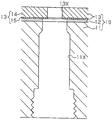
이하, 정전 척(1)의 일 실시형태를 도 1a 내지 도 6을 참조하여 설명한다.Hereinafter, an embodiment of the
정전 척(1)은, 종례 예의 정전 척(80)과 마찬가지로, 베이스(10), 점착층(20), 점착층(20)에 의해 베이스(10)에 본딩된 정전 척(ESC) 흡인 플레이트(30), ESC 흡인 플레이트(30) 내에 내장된 흡인 전극(40), 및 흡인 전극(40)에 전기적으로 접속된 커넥터(50)를 포함한다.The
베이스(10)는 ESC 흡인 플레이트(30)를 지지한다. 베이스(10)는 베이스 플레이트(11), 점착층(12), 및 히터 플레이트(13)를 포함한다. 히터 플레이트(13)는 점착층(12)에 의해 베이스 플레이트(11)에 본딩된다.
베이스 플레이트(11)는 전도성 재료로 형성될 있다. 예를 들면, 베이스 플레이트(11)는 알루미늄 또는 초경합금 등의 금속 재료, 또는 금속 재료와 세라믹 재료의 복합 재료로 형성될 수 있다. 바람직한 예에서는, 베이스 플레이트(11)는 취득 및 처리가 쉽고 열 전도성이 양호한 알루미늄 또는 알루미늄 합금으로 형성된다. 베이스 플레이트(11)는 절연층이 형성된 양극 처리된 표면을 갖는다. 베이스 플레이트(11)는, 예를 들면 약 35 ㎜ 내지 40㎜의 두께를 가질 수 있다.The
점착층(12)은 주로 베이스 플레이트(11)와 히터 플레이트(13) 사이의 열 전도성을 향상시키는데 사용된다. 일 예에서, 히터 플레이트(13)는 ESC 흡인 플레이트(30) 상에 유지된 흡인 대상(예를 들면, 실리콘 웨이퍼)을 가열한다. 그러나, 흡인 대상이, 예를 들면 플라즈마에 의해 빠르게 가열될 경우, 열이 방출될 필요가 있다. 또한, 흡인 대상이 가열되는 동안, 히터 플레이트(13)로부터의 열 또한 베이스 플레이트(11)에 전달될 필요가 있다. 따라서, 점착층(12)은 열 전도성이 높은 재료로 형성되는 것이 바람직하다. 예를 들면, 점착층(12)은 실리콘 수지로 형성될 수 있다. 점착층(12)은, 예를 들면 약 0.5㎜ 내지 2.0㎜의 두께를 가질 수 있다.The
히터 플레이트(13)는 금속 플레이트(14), 및 금속 플레이트(14)의 하면(14A)에 본딩되는 히터(15)의 막을 포함한다. 전압의 공급 시 열을 발생시키는 히터(15)는 점착층(20)을 거쳐 ESC 흡인 플레이트(30)를 제어 온도로 유지한다. 히터(15)는 점착층(12)에 의해 베이스 플레이트(11)에 본딩된다. 금속 플레이트(14)는 소킹 플레이트(soaking plate)로서 기능한다. 금속 플레이트(14)는, 예를 들면 알루미늄 또는 알루미늄 합금으로 형성될 수 있다. 금속 플레이트(14)는, 예를 들면 약 1.5㎜ 내지 1.8㎜의 두께를 가질 수 있다. 히터(15)는, 예를 들면 약 0.1㎜ 내지 0.5㎜의 두께를 가질 수 있다.The
히터(15)는, 예를 들면 폴리이미드 수지의 막에 소정의 형상의 히터 전극(메탈 와이어)을 패터닝하고, 다른 폴리이미드 수지막을 형성해서 히터 전극이 폴리이미드 수지막들 사이에 개재되게 하고, 상기 막들을 열 경화하여 막들과 히터 전극을 일체화함으로써 형성될 수 있다. 히터 플레이트(13)는 히터(15)를 금속 플레이트(14)에 본딩함으로써 형성될 수 있다. 히터 전극은, 인코넬(Inconel; 등록 상표) 등의 전도성 재료로 형성될 수 있다. 인코넬(등록 상표)은, 주성분이 니켈(Ni)이고 크롬(Cr)이 약 15% 내지 23%이고, 철(Fe), 코발트(Co), 또는 몰리브덴(Mo)을 더 함유할 수 있는 내열성 합금이다. 인코넬은 가공성이 높고, 열 처리 및 냉각 처리 모두 가능하며, 내식성이 높다.The
점착층(20)은 주로 히터 플레이트(13)와 ESC 흡인 플레이트(30) 사이의 열 전도성을 양호하게 유지하는 데 사용된다. 점착층(20)은 실리콘 등의 고전도성 재료로 형성될 수 있는 것이 바람직하다. 점착층(20)은 히터 플레이트(13)의 상면과 ESC 흡인 플레이트(30)의 하면 사이에 형성될 수 있다. 점착층(20)은, 예를 들면 0.05㎜ 내지 0.2㎜의 두께를 가질 수 있다.The
ESC 흡인 플레이트(30)는 흡인 대상을 정전기적으로 유지하는 흡인면(30A)(도 1a에서 상면)을 갖는다. ESC 흡인 플레이트(30)는 절연 재료로 형성될 수 있다. 예를 들면, ESC 흡인 플레이트(30)는 알루미늄, 질화알루미늄, 및 질화실리콘 등의 세라믹 재료, 또는 실리콘 수지 및 폴리이미드 수지 등의 유기 재료로 형성될 수 있다. 예시되는 예에서, ESC 흡인 플레이트(30)는 취득 및 처리가 쉽고 플라즈마 저항성이 상대적으로 매우 높은 알루미늄 또는 질화알루미늄 등의 세라믹 재료로 형성된다. ESC 흡인 플레이트(30)가 150W/(m*K) 내지 250W/(m*K)의 열 전도성이 높은 질화알루미늄으로 형성될 수 있는 것이 더 바람직한다. 질화알루미늄은 ESC 흡인 플레이트(30) 상에 유지된 흡인 대상의 평면 온도 변화를 줄이므로 바람직하다. ESC 흡인 플레이트(30)는 흡인면(30A)에 흡인되는 흡인 대상(예를 들면, 직경 300㎜)보다 약간 작을 수 있다. 이로 인해, 적어도 흡인면(30A)이 플라즈마에 노출되는 것이 방지된다. ESC 흡인 플레이트(30)는, 예를 들면 약 2㎜ 내지 10㎜의 두께를 가질 수 있다.The
흡인 전극(40)은 ESC 흡인 플레이트(30)에 임베드된다. 흡인 전극(40)은 ESC 흡인 플레이트(30)의 흡인면(30A)에 가깝게 형성되는 전극층(41), 전극층(41)에 전기적으로 접속되는 제 1 배선층(42), 및 제 1 배선층(42)에 전기적으로 접속되는 제 2 배선층(43)을 포함할 수 있다. 전극층(41)은 정전 흡인을 위해 DC 전압이 공급되는 박막 정전기 전극이다. 제 1 배선층(42) 및 제 2 배선층(43)은 전극층(41)을 ESC 흡인 플레이트(30) 아래의 층에 접속하는 데 사용된다. ESC 흡인 플레이트(30)는 세라믹 재료로 형성된다. 따라서, 전극층(41), 제 1 배선층(42), 및 제 2 배선층(43)은 텅스텐(W), 몰리브덴, 또는 구리(Cu)로 형성될 수 있는 것이 바람직하다. 원하는 ESC 흡인 플레이트(30)는, 예를 들면 소정의 두께로 적층된 세라믹 그린 시트에 전극층(41), 제 1 배선층(42), 및 제 2 배선층(43)을 패터닝하는 후막(thick film) 처리를 행하고, 세라믹 재료가 층들로 배치되는 일체로 적층된 층을 베이킹함으로써 형성될 수 있다. ESC 흡인 플레이트(30)의 하면으로부터 전극층(41)의 하면까지의 두께는, 예를 들면 약 1.8㎜ 내지 9.4㎜일 수 있다. 전극층(41)의 상면으로부터 ESC 흡인 플레이트(30)의 흡인면(30A)까지의 두께는, 예를 들면 약 0.2㎜ 내지 0.6㎜일 수 있다. ESC 흡인 플레이트(30)는 플라즈마를 제어하는 고주파 전력이 공급되는 복수의 RF 전극층을 포함할 수 있다. RF 전극층은 흡인면(30A)에 반대측인 ESC 흡인 플레이트(30)의 하면 또는 ESC 흡인 플레이트(30)의 하부에 임베드된다.
이하, 흡인 전극(40)과 흡인 전극(40)에 DC 전압을 공급하는 DC 전원 공급 장치를 접속하는 커넥터(50)를 설명한다. 커넥터(50)는 전원 공급 컴포넌트 또는 소켓이라고 할 수 있다.Hereinafter, the
스루홀(11X)은 베이스 플레이트(11) 및 점착층(12)을 베이스 플레이트(11) 및 점착층(12)의 두께 방향으로 관통 연장된다. 스루홀(13X)은 스루홀(11X)과 정렬하여 히터 플레이트(13)의 히터(15) 및 금속 플레이트(14)를 관통 연장된다. 스루홀(13X)은 스루홀(11X)과 연통한다. 스루홀(13X)은 스루홀(11X)보다 개구 직경이 작다. 도 1b에 나타낸 바와 같이, 스루홀(13X)의 테두리 및 벽을 포함하는 히터 플레이트(13)의 부분은, 위에서 봤을 때, 스루홀(11X)의 테두리로부터 내측으로 돌출되는 돌출부(13A)로서 기능한다. 돌출부(13A) 및 스루홀(11X)의 벽은 단차를 형성한다. 도시된 예에서, 베이스(10)는 베이스 플레이트(11)와 히터 플레이트(13) 사이에 형성된 단차를 갖는다. 베이스 플레이트(11), 점착층(12), 히터(15), 및 금속 플레이트(14)를 두께 방향으로 관통 연장되는 스루홀(11X 및 13X)은 베이스(10)를 두께 방향으로 관통 연장되는 일례로서의 제 1 스루홀을 형성한다. 스루홀(11X)은, 예를 들면 원형일 수 있고 스루홀(11X)이 스루홀(13X)과 연통하는 테두리에서 약 4㎜ 내지 5㎜의 직경을 가질 수 있다. 스루홀(13X)은, 예를 들면 원형일 수 있고, 예를 들면 약 2㎜ 내지 3㎜의 직경을 가질 수 있다.The through
히터 플레이트(13)에는, 절연체(60)가 본딩된다. 일 예에서, 절연체(60)는 점착제(도시 생략)에 의해 히터 플레이트(13)의 돌출부(13A)에 본딩된다. 절연체(60)는 스루홀(61X)을 갖는 베이스(61), 베이스(61)의 상면으로부터 연장되는 제 1 관 형상부(62), 및 베이스(61)의 하면으로부터 연장되는 제 2 관 형상부(63)를 포함한다. 베이스(61), 제 1 관 형상부(62), 및 제 2 관 형상부(63)는 일체로 형성된다. 제 1 관 형상부(62)는 스루홀(61X)과 연통하고, 스루홀(61X)보다 직경이 큰 개구(62X)를 포함한다. 제 2 관 형상부(63)는 스루홀(61X)과 연통하고, 스루홀(61X) 및 개구(62X)보다 직경이 큰 개구(63X)를 포함한다. 제 1 관 형상부(62)의 외면은 돌출부(13A)의 내면에 본딩되고, 제 1 관 형상부(62)로부터 외측으로 연장되는 베이스(61)의 상면의 부분은 돌출부(13A)의 하면에 본딩된다. 절연체(60)의 상면(제 1 관 형상부(62)의 상면)은 히터 플레이트(13)의 상면(금속 플레이트(14)의 상면)과 동일 평면을 이룬다. 베이스(61)는, 예를 들면 약 1.7㎜ 내지 1.9㎜의 두께를 가질 수 있다. 스루홀(61X)은 위에서 봤을 때 원형일 수 있고, 예를 들면 약 1.2㎜ 내지 1.5㎜의 두께를 가질 수 있다. 개구(62X)는 위에서 봤을 때 원형일 수 있고, 예를 들면 약 1.6㎜ 내지 1.8㎜의 두께를 가질 수 있다. 개구(63X)는 위에서 봤을 때 원형일 수 있고, 예를 들면 약 2㎜ 내지 3㎜의 두께를 가질 수 있다. 절연체(60)는 절연 재료, 예를 들면 가소성 재료 등의 수지 재료로 형성될 수 있다.The
ESC 흡인 플레이트(30)는 히터 플레이트(13)의 스루홀(13X)과 정렬되는 오목부(30X)를 포함한다. 오목부(30X)는 제 2 배선층(43)의 하면이 적어도 부분적으로 노출되게 한다. 오목부(30X)는 스루홀(13X 및 11X)과 연통한다. 예를 들면, 히터 플레이트(13)에 절연체(60)를 본딩할 때, 오목부(30X)는, 절연체(60)의 개구(62X) 및 스루홀(61X)의 개구(63X)를 거쳐 베이스 플레이트(11)의 스루홀(11X)과 연통한다. 오목부(30X)는 히터 플레이트(13)의 스루홀(13X)보다 직경이 작고 제 1 관 형상부(62)의 개구(62X)보다 직경이 크다. 오목부(30X)는 절연체(70)(후술함)를 수용하도록 충분히 깊다. 일 예에서, 오목부(30X)의 깊이는 흡인 전극(40)에 인가되는 DC 전압의 값 및 오목부(30X) 내에 형성된 점착층(20)의 브레이크다운 전압(breakdown voltage) 특성에 따라 설정될 수 있다. 오목부(30X)는, 예를 들면 약 1.3㎜ 내지 1.5㎜의 깊이를 가질 수 있다.The
절연체(60)의 제 1 관 형상부(62)의 개구(62X)로부터 노출되는 베이스(61)의 상면에 관 형상인 절연체(70)가 배치된다. 절연체(70)는 개구(62X)(스루홀(13X))를 두께 방향(상방)으로 관통 연장되고, 또한 오목부(30X)에서 두께 방향(상방)으로 연장된다. 절연체(70)의 선단부는 ESC 흡인 플레이트(30)의 오목부(30X) 내에 배치된다. 도시된 예에서, 절연체(70)의 선단부는 오목부(30X)의 중간 위치에 두께 방향으로 연장된다. 절연체(70)는 모든 재료로 형성될 수 있으며, 예를 들면 가소성 재료 등의 수지 재료일 수 있다.A
절연체(70)는 관 형상이며 관을 따라 연장되는 스루홀(70X)을 갖는다. 스루홀(70X)은 베이스(61)의 스루홀(61X)과 연통한다. 스루홀(70X)은 스루홀(61X)과 실질적으로 동일한 직경을 갖는다. 도시된 예에서, 절연체(70)는, 히터 플레이트(13)와 ESC 흡인 플레이트(30)을 본딩하는 점착층(20)에 의해 적어도 ESC 흡인 플레이트(30)에 본딩된다.The
점착층(20)은 히터 플레이트(13)와 ESC 흡인 플레이트(30) 사이, 또한 절연체(60)와 절연체(70) 사이에 형성된다. 예를 들면, 점착층(20)은 절연체(70)의 외면과 제 1 관 형상부(62)의 내면 사이에 형성된다. 도시하지 않았지만, 점착층(20)은 절연체(70)의 하면과 베이스(61)의 상면 사이에도 형성된다. 도시된 예에서, 점착층(20)은 오목부(30X)의 내면 및 절연체(70)의 선단부의 상면을 전체적으로 덮는다. 점착층(20)은 절연체(70)의 선단부의 상면에 형성된 개구 단부에 대응하는 개구 단부를 포함한다.The
스루홀(11X 및 13X) 및 오목부(30X)는 커넥터(50)를 수용하는 형상으로 된다. 도시된 예에서, 커넥터(50)는 스루홀(11X), 절연체(60)의 개구(63X) 및 스루홀(61X), 절연체(70)의 스루홀(70X), 및 ESC 흡인 플레이트(30)의 오목부(30X)에 배치된다. 커넥터(50)는 절연 재료로 형성된 관(51), 관(51) 내에 배치되며 관(51)에 고정된 유지부(52), 관(51) 내에 배치되며 유지부(52)에 결합된 탄성 부재(53), 관(51) 내에 부분적으로 배치되며 탄성 부재(53)에 결합된 전원 단자(54)를 포함할 수 있다. 탄성 부재(53)는, 예를 들면 스프링일 수 있다.The through
관(51)은, 관(51)을 베이스 플레이트(11)에 고정하도록, 베이스 플레이트(11) 내의 스루홀(11X)의 하부와 체결되는 나사식 기단부(51A)를 포함한다. 관(51)의 선단부는 절연체(60)의 개구(62X) 내에 배치된다. 관(51)은 유지부(52) 및 탄성 부재(53)를 둘러싸고 전원 단자(54)를 부분적으로 둘러싼다. 관(51)은 베이스 플레이트(11)로부터, 관(51) 내에 삽입되는 유지부(52) 및 전원 단자(54)를 절연하는 기능을 한다. 관(51)은 모든 절연 재료로 형성될 수 있으며, 가소성 재료 등의 수지 재료를 포함할 수 있다.The
유지부(52)는, 예를 들면 점착제(도시 생략)로 관(51)에 고정된다. 유지부(52)는 정전 척(1)의 외측에 배치되는 DC 전원 공급 장치에 전기적으로 접속되는 파워 코드(power cord)(도시 생략)를 수용 및 지지한다. 파워 코드는 전원 단자(54)에 전기적으로 접속된다. 탄성 부재(53)는 유지부(52)의 선단부와 전원 단자(54)의 기단부 사이에 배치된다. 전원 단자(54)의 선단부는 관(51)으로부터 수직 방향에서 상방으로 돌출된다. 전원 단자(54)의 선단부는 오목부(30X)로부터 노출된 제 2 배선층(43)의 하면과 접촉한다. 이로 인해, 제 2 배선층(43)은 전원 단자(54), 파워 코드 등을 거쳐 DC 전원 공급 장치에 전기적으로 접속됨으로써, 전극층(41)과 DC 전원 공급 장치를 전기적으로 접속한다. 탄성 부재(53)는 전원 단자(54)를 제 2 배선층(43)을 향해 탄성적으로 돌출시킨다. 따라서, 전원 단자(54)의 선단부는 제 2 배선층(43)에 가압된다. 이러한 구조로 인해, 다양한 컴포넌트의 결합으로 야기되는 치수 오차에 상관없이, 전원 단자(54)를 제 2 배선층(43)에 전기적으로 접속시킬 수 있다.The holding
관(51)으로부터 돌출되는 전원 단자(54)는 절연체(60 및 70) 및 점착층(20)에 의해 둘러싸인다. 환언하면, 절연체(60 및 70) 및 점착층(20)은, 전원 단자(54)가 제 2 배선층(43)과의 접촉 시에 전원 단자(54)를 둘러싸도록 형성된다. 도 1b에 도시된 예에서, 절연체(60)(제 2 관 형상부(63))는 관(51)으로부터 돌출되는 전원 단자(54)를 둘러싸도록 스루홀(11X) 내에 형성된다. 스루홀(11X) 내에 형성된 절연체(60)는 전원 단자(54) 및 베이스 플레이트(11)를 절연한다. 스루홀(13X) 내에서, 절연체(60 및 70) 및 점착층(20)은 전원 단자(54)를 둘러싸도록 형성된다. 스루홀(13X) 내에 형성된 절연체(60 및 70) 및 점착층(20)은 전원 단자(54) 및 히터 플레이트(13)를 절연하도록 기능한다. 구체적으로, 스루홀(13X) 내에서 전원 단자(54) 및 히터 플레이트(13)는 3개의 절연체(절연체(60 및 70) 및 점착층(20))에 의해 서로 분리된다. 오목부(30X) 내에서, 절연체(70) 및 점착층(20)은 전원 단자(54)를 둘러싸도록 형성된다. 오목부(30X) 내에 형성된 절연체(70) 및 점착층(20)은 전원 단자(54) 및 히터 플레이트(13)(금속 플레이트(14))를 절연하도록 기능한다. 오목부(30X) 내에서, 전원 단자(54) 및 히터 플레이트(13)는 2개의 절연체(절연체(70) 및 점착층(20))에 의해 서로 분리된다.The
ESC 흡인 플레이트(30) 및 흡인 대상이 반대 전하를 띠도록, 정전 척(1)은 커넥터(50)를 거쳐(전원 단자(54)를 포함) 흡인 전극(40)에 DC 전압을 인가한다. 이로 인해, ESC 흡인 플레이트(30)의 흡인면(30A)에 흡인 대상을 유지하는 정전기력(쿨롱힘)이 발생된다. 흡인 전극(40)에 인가되는 전압의 증가는 정전기 유지력을 증가시킨다.The
이하, 정전 척(1)의 동작을 설명한다.The operation of the
정전 척(1)에서, ESC 흡인 플레이트(30)는, 전극층(41)에 접속되는 제 2 배선층(43)을 노출시키는 오목부(30X), 오목부(30X)에 형성된 절연체(70), 및 오목부(30X)의 내면 전체를 덮도록 형성된 점착층(20)을 포함한다. 이로 인해, 제 2 배선층(43)에 전기적으로 접속되는 전원 단자(54)의 선단부를 2개의 절연체, 즉 절연체(70) 및 점착층(20)에 의해 둘러싸이게 할 수 있다. 따라서, 이러한 구조는 전원 단자(86A)의 선단부(86B)와 베이스(81) 사이에 점착층(82)만이 배치되는 구조(도 8 참조)보다, 전원 단자(54)의 선단부와 히터 플레이트(13)(금속 플레이트(14)) 사이에 두꺼운 절연을 제공할 수 있다. 이로 인해, 전원 단자(54)와 금속 플레이트(14) 사이의 절연의 신뢰성이 향상된다. 전원 단자(54)는 소켓의 가늘고 긴 선단 단자의 일례이다.In the
이하, 정전 척(1)의 제조 방법을 간략히 설명한다.Hereinafter, the manufacturing method of the
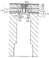
도 2a에 나타낸 바와 같이, 점착층(12)이 베이스 플레이트(11)와 히터 플레이트(13) 사이에 배치되는 상황에서, 베이스 플레이트(11)의 스루홀(11X)이 히터 플레이트(13)의 스루홀(13X)과 정렬되도록, 베이스 플레이트(11) 및 히터 플레이트(13)가 위치 결정된다. 이어서, 점착층(12)이 경화(열 경화)되어, 베이스 플레이트(11)를 점착층(12)과 함께 히터 플레이트(13)에 본딩한다. 이로써, 베이스 플레이트(11) 및 히터 플레이트(13)를 포함하는 베이스(10)가 완성되며, 스루홀(11X)이 두께 방향으로 연장된다.As shown in FIG. 2A, in the situation where the
도 2b에 나타낸 공정에서, 절연체(60)의 베이스(61)의 상면 및 제 1 관 형상부(62)의 외면에 의해 형성된 단차가 히터 플레이트(13)의 돌출부(13A)와 접촉할 때까지, 점착제(도시 생략)로 피복된 표면을 갖는 절연체(60)가 하방으로부터 베이스 플레이트(11)의 스루홀(11X) 내로 삽입된다. 이어서, 점착제가 경화되어 히터 플레이트(13) 및 절연체(60)가 점착제와 함께 본딩된다.In the process shown in FIG. 2B, until the step formed by the upper surface of the
도 3a에 나타낸 공정에서, 베이스(10)(금속 플레이트(14))의 상면과 절연체(60)(제 1 관 형상부(62))의 상면이 서로 동일 평면이 되도록, 베이스(10) 및 절연체(60)는 평탄화된다. 구체적으로, 베이스(10)(금속 플레이트(14)) 및 절연체(60)의 상면은 연삭 및 연마를 통해 평탄화된다. 연삭 또는 연마는, 예를 들면 탄화텅스텐 또는 다이아몬드 연삭 비트(툴)에 의한 툴 비트 연삭을 포함한다. 또는, 연삭 또는 연마는 CMP(chemical mechanical polishing)를 포함할 수 있다.In the process shown in FIG. 3A, the
도 3b에 나타낸 공정에서, 절연체(70)는, 히터 플레이트(13)의 스루홀(13X)의 상방으로부터 절연체(60)의 제 1 관 형상부(62)의 개구(62X) 내로 끼워 맞춰진다. 절연체(70)는 절연체(60)의 베이스(61)의 상면에 배치되며 개구(62X)로부터 노출된다. 오목부(30X)를 절연체(70)의 스루홀(70X)과 정렬하도록 위치 결정된 ESC 흡인 플레이트(30)가 점착층(20)으로 베이스(10)에 본딩된다. 이로써, ESC 흡인 플레이트(30)의 오목부(30X) 내에 절연체(70)의 선단부가 배치된다. 이 공정에서, 점착층(20)은, ESC 흡인 플레이트(30)의 하면과 금속 플레이트(14)의 상면 사이에 형성되며, 또한 오목부(30X)를 충전한다. 점착층(20)은 절연체(70)의 외면과 절연체(60)의 제 1 관 형상부(62)의 내면 사이에 더 형성된다. 환언하면, 오목부(30X) 내에서 ESC 흡인 플레이트(30)의 하면과 금속 플레이트(14)의 상면 사이, 및 절연체(70)의 외측과 절연체(60)의 내면 사이에 점착층(20)이 형성되도록, ESC 흡인 플레이트(30)가 베이스(10) 상에 탑재된다. 베이스(10)와 ESC 흡인 플레이트(30) 사이에 제어된 두께를 갖도록, 점착층(20)이 형성된다. 점착층(20)은 절연체(70)를 절연체(60)에 본딩한다.In the process shown in FIG. 3B, the
도 4에 나타낸 공정에서, 도 3b의 공정에서 형성된 점착층(20)으로부터 과잉 부분은 제거된다. 예를 들면, 스루홀(70X) 내에 형성된 점착층(20)의 부분 및 스루홀(70X) 위로 형성되며 제 2 배선층(43)의 하면을 덮는 점착층(20)의부분이 제거된다. 이로 인해, ESC 흡인 플레이트(30)의 오목부(30X) 내에서 전극층(41)에 전기적으로 접속되는 제 2 배선층(43)의 하면을 노출시킨다.In the process shown in FIG. 4, excess portions are removed from the pressure-
도 4에 나타낸 공정에서, ESC 흡인 플레이트(30)의 상면은 연삭 또는 연마되고 평탄화된다. 연삭 및 연마는, 예를 들면 툴 비트 연삭 또는 CMP일 수 있다.In the process shown in FIG. 4, the top surface of the
도 5에 나타낸 공정에서, 유지부(52), 탄성 부재(53), 및 전원 단자(54)를 포함하는 전원 공급 유닛(55)이 관(51) 내로 삽입되며 점착제(도시 생략)에 의해 관(51)에 본딩된다. 예를 들면, 유지부(52)는 점착제에 의해 관(51)에 본딩된다. 이로써, 도 1에 나타낸 커넥터(50)가 완성된다. 커넥터(50)의 기단부(51A)는 스루홀(11X)에 체결되어 커넥터(50)를 베이스(10)에 고정한다. 탄성 부재(53)는, 전원 단자(54)가 제 2 배선층(43)과 접촉하도록 전원 단자(54)에 탄성력을 가한다. 상술한 공정은 도 1에 나타낸 정전 척(1)을 형성한다.In the process shown in FIG. 5, a
스루홀(11X)은 제 3 스루홀의 일례이다. 스루홀(13X)은 제 4 스루홀의 일례이다. 점착층(20)은 제 1 점착층의 일례이다. 점착층(12)은 제 2 점착층의 일례이다. 절연체(70)는 제 1 절연층의 일례이다. 스루홀(70X)은 제 2 스루홀의 일례이다. 절연체(60)는 제 2 절연층의 일례이다. 절연체(70) 및 점착층(20)은 오목부(30X) 내에 전원 단자(54)를 둘러싸는 2층 절연 구조체를 형성한다. 절연체(70), 절연체(60)의 제 1 관 형상부(62), 및 절연체(70)와 제 1 관 형상부(62)를 본딩하는 점착층(20)의 관 형상 부분은 스루홀(13X) 내에 전원 단자(54)를 둘러싸는 3층 절연 구조체를 형성한다.The through
이하, 혹독한 조건에서 정전 척(1)에 행해진 연속되는 실험 결과를 도 6을 참조하여 설명한다.Hereinafter, the results of continuous experiments performed on the
절연 성능을 평가하기 위해, 샘플 1 내지 샘플 10을 준비했다. 샘플 1 내지 샘플 5는 도 1의 정전 척(1)과 동일한 구조를 가졌다. 샘플 1 내지 샘플 5 각각은 가소성 절연체(70)를 수용하는 깊이가 1.3㎜인 오목부(30X)를 포함한다. 샘플 1 내지 샘플 5 각각의 오목부(30X)의 내면은 실리콘 수지로 형성되는 점착층(20)에 의해 전체적으로 덮인다. 비교 샘플 6 내지 비교 샘플 10은 도 8에 나타낸 종례 예의 정전 척과 동일한 구조를 갖는다. 또한, 비교 샘플 6 내지 비교 샘플 10 각각은 도 1에 나타낸 오목부(30X) 및 절연체(70) 모두를 포함하지 않으며, 전원 단자와 베이스 사이에 배치되는 절연체는 실리콘 수지로 형성되는 점착층뿐이다.In order to evaluate the insulation performance,
샘플 1 내지 샘플 10 각각의 정전 척에서는, 전극에 DC 전압이 인가되었다. DC 전압을 0V 내지 10㎸로 점착 증가시켜서 전원 단자와 베이스 사이에 방전이 일어났는지의 여부를 검사했다. 도 6은 그 결과를 나타낸다.In the electrostatic chucks of each of
종례 예와 동일한 구조를 갖는 샘플 6 내지 샘플 10에서는, DC 전압이 10㎸에 도달하기 전에 전원 단자와 베이스 사이에 방전이 일어났다. 도 1에 나타낸 구조를 갖는 샘플 1 내지 샘플 5에서는, 흡인 전극(40)에 10㎸의 DC 전압이 인가되었을 경우에도, 전원 단자(54)와 베이스(10)의 금속 플레이트(14) 사이에 방전이 일어나지 않았다. 이 결과는, 상대적으로 깊은 오목부(30X)에 배치된 2개의 절연체, 즉 절연체(70) 및 절연용 점착층(20)이 전원 단자(54)와 금속 플레이트(14) 사이의 절연의 신뢰성을 향상시킴을 보여준다.In Samples 6 to 10 having the same structure as in the case example, discharge occurred between the power supply terminal and the base before the DC voltage reached 10 mA. In
상기 실시형태는 후술하는 이점을 갖는다.The said embodiment has the advantage mentioned later.
(1) ESC 흡인 플레이트(30)는 흡인 전극(40)(특히, 전극층(41)에 접속되는 제 2 배선층(43))을 적어도 부분적으로 노출하는 오목부(30X)를 포함한다. 절연체(70)는 오목부(30X) 내에 배치된다. 오목부(30X)의 내면 전체는 점착층(20)에 의해 덮인다. 이 구조에서, 전원 단자(54)가 흡인 전극(40)에 전기적으로 접속되는 상황에서, 전원 단자(54)의 선단부는 2개의 절연체, 즉 절연체(70) 및 점착층(20)에 의해 둘러싸인다. 이 구조는 전원 단자(54)와 히터 플레이트(13)(금속 플레이트(14)) 사이의 절연 두께를 증가시킴으로써, 전원 단자(54)와 금속 플레이트(14) 사이의 절연의 신뢰성을 향상시킨다. 또한, 이 구조는 전원 단자(54)와 베이스(10)의 금속 플레이트(14) 사이의 방전을 저감 또는 방지하여 정전 척(1)의 내구성을 향상시킨다.(1) The
전원 단자(54)의 선단부 및 금속 플레이트(14)는, 점착층(20)만이 아닌, 실리콘 수지 점착층(20) 및 절연체(70)에 의해 서로 절연된다. 따라서, 점착층(20) 내에 보이드가 형성될 경우에도, 절연체(70)는 금속 플레이트(14)로부터 전원 단자(54)의 선단부를 절연한다.The tip portion of the
(2) 오목부(30X)는 흡인 전극(40)에 인가되는 DC 전압의 값 및 오목부(30X) 내에 형성되는 점착층(20)의 브레이크다운 전압 특성에 따라 설정된 깊이를 갖는다. 예를 들면, 흡인 전극(40)에 약 10㎸의 DC 전압이 인가될 경우, 점착층(20)(예를 들면, 실리콘 수지)의 브레이크다운 전압 특성은 12㎸/㎜이다. 이 경우에, 오목부(30X)는 0.8㎜ 이상의 깊이를 갖는 것이 바람직하다(0.8*12=9.6㎸). 본 실시형태에서, 오목부(30X)는 1㎜ 이상의 깊이를 갖는다(예를 들면, 약 1.3㎜ 내지 1.5㎜). 이로 인해, 흡인 전극(40)에 약 10㎸의 DC 전압이 인가될 경우에도, 전원 단자(54)와 금속 플레이트(14) 사이의 방전을 효과적으로 저감 또는 방지할 수 있다. 이러한 방식으로, 오목부(30X)의 깊이의 최적 조정은 방전을 저감 또는 방지한다. 따라서, 흡인 전극(40)에 원하는 DC 전압의 인가가 가능해지면서 정전 척(1)의 내구성이 쉽게 향상될 수 있다.(2) The
본 발명의 사상 또는 범주에서 벗어나지 않고, 본 발명이 많은 다른 특정 형태로 구현될 수 있음은 당업자에게 명확하다. 특히, 본 발명의 다음의 형태로 구현될 수 있음을 이해할 것이다.It is apparent to those skilled in the art that the present invention can be embodied in many other specific forms without departing from the spirit or scope of the invention. In particular, it will be understood that the following forms of the invention may be implemented.
오목부(30X)의 내면 전체가 점착층(20)에 의해 덮이는 것이 바람직하지만, 오목부(30X)의 내면이 점착층에 의해 덮일 수 있다. 또한, 이 변형은 2개의 절연체, 즉 점착층(20) 및 절연체(70)가 금속 플레이트(14)로부터 오목부(30X) 내에 위치된 전원 단자(54)를 절연하도록 할 수 있다. 이 구조는 전원 단자(54)와 금속 플레이트(14) 사이의 절연의 신뢰성을 향상시킨다.Although the whole inner surface of the recessed
절연체(70)의 선단부는 제 2 배선층(43)의 하면에 접촉하도록 연장될 수 있다. 이로 인해, 절연체(70) 및 점착층(20)은 전원 단자(54)의 선단부 전체를 둘러싸는 것이 보장되며, 2개의 절연체, 즉 절연체(70) 및 점착층(20)이 금속 플레이트(14)로부터 오목부(30X) 내에 배치된 전원 단자(54)를 절연할 수 있게 한다.The tip portion of the
상기 실시형태에서 금속 플레이트(14)는 생략될 수 있다.In the above embodiment, the
상기 실시형태에서 히터(15)는 ESC 흡인 플레이트(30) 전체에 배치된 단일 히터 전극 또는 ESC 흡인 플레이트(30) 내에 규정된 복수의 히터 존에 따라 배치된 복수의 히터 전극을 포함할 수 있다. 히터(15)는 별개의 존에 복수의 히터 전극을 포함할 경우, ESC 흡인 플레이트(30)의 히터 존은 별개로 가열될 수 있다.In the above embodiment, the
상기 실시형태에서, 절연체(70)는 절연체(60)에 본딩된다. 대신, 예를 들면 절연체(60 및 70)는 일체로 형성될 수 있고, 일체로 된 절연체가 스루홀(11X)에 배치될 수 있다.In the above embodiment, the
상기 실시형태에서, 전원 단자(54)가 제 2 배선층(43)과 접촉하여 전원 단자(54)와 제 2 배선층(43)을 전기적으로 접속하도록, 탄성 부재(53)는 커넥터(50)의 전원 단자(54)에 탄성력을 가한다. 대신, 예를 들면, 커넥터(50)의 전원 단자가 솔더 등에 의해 제 2 배선층(43)에 전기적으로 접속될 수 있다.In the above embodiment, the
정전 척(1)은 단극 정전 척 또는 양극 정전 척일 수 있다.The
정전 척(1)은 쿨롱 정전 척 또는 존슨-라벡 정전 척일 수 있다.The
상기 변형의 두 가지 이상이 조합될 수 있다.Two or more of the above variations may be combined.
본 예 및 실시형태는 예시이지 제한이 아닌 것으로 간주되어야 하며, 본 발명은 여기에서 제시된 상세로 한정되는 것이 아니라, 첨부된 특허청구범의 범주 및 그 등가물 내에서 변형될 수 있다.The present examples and embodiments are to be considered as illustrative and not restrictive, and the invention is not to be limited to the details set forth herein, but may be modified within the scope and equivalents of the appended claims.
1 : 정전 척 10 : 베이스
11 : 베이스 플레이트 12 : 점착층
13 : 히터 플레이트 14 : 금속 플레이트
15 : 히터 20 : 점착층
30 : ESC 흡인 플레이트 40 : 흡인 전극
41 : 전극층 42 : 제 1 배선층
43 : 제 2 배선층 50 : 커넥터
51 : 관 52 : 유지부
53 : 탄성 부재 54 : 전원 단자
60 : 절연체 61 : 베이스
62 : 제 1 관 형상부 63 : 제 2 관 형상부
70 : 절연체1: electrostatic chuck 10: base
11: base plate 12: adhesive layer
13: heater plate 14: metal plate
15
30: ESC suction plate 40: suction electrode
41
43: second wiring layer 50: connector
51
53: elastic member 54: power supply terminal
60: insulator 61: base
62: first tubular portion 63: second tubular portion
70: Insulator
Claims (12)
상기 베이스에 본딩된 정전 척 흡인 플레이트,
상기 정전 척 흡인 플레이트 내에 내장되고, 정전하를 발생시켜 정전 척으로 흡인 대상을 정전기적으로 흡인하는 흡인 전극,
상기 베이스의 상기 제 1 스루홀과 정렬되어 상기 정전 척 흡인 플레이트 내에 형성되고, 상기 흡인 전극을 부분적으로 노출시키는 오목부,
상기 정전 척 흡인 플레이트와 상기 베이스 사이에 형성되고, 상기 오목부의 내면을 덮는 점착층,
상기 오목부 내에 배치되고, 제 2 스루홀을 포함하는 관 형상 절연체, 및
상기 베이스의 상기 제 1 스루홀 및 상기 관 형상 절연체의 상기 제 2 스루홀 내에 배치되고, 상기 오목부로부터 노출된 상기 흡인 전극에 전기적으로 접속되는 선단부를 포함하는 전원 단자를 포함하는 정전 척.A base including a first through hole extending through the thickness direction,
An electrostatic chuck suction plate bonded to the base,
A suction electrode embedded in the electrostatic chuck suction plate and generating an electrostatic charge to electrostatically attract the object to be sucked by the electrostatic chuck;
A recess formed in the electrostatic chuck suction plate aligned with the first through hole of the base and partially exposing the suction electrode,
An adhesive layer formed between the electrostatic chuck suction plate and the base and covering an inner surface of the recess;
A tubular insulator disposed in said recess and comprising a second through hole, and
And a power supply terminal disposed within said first through hole of said base and said second through hole of said tubular insulator, said power supply terminal including a leading end electrically connected to said suction electrode exposed from said recess.
상기 점착층은 상기 오목부의 내면 전체를 덮는 정전 척.The method of claim 1,
The adhesive layer covers the entire inner surface of the recess.
상기 절연체는 상기 오목부로부터 노출된 상기 흡인 전극과 접촉하는 선단부를 포함하는 정전 척.3. The method according to claim 1 or 2,
The insulator includes an end portion in contact with the suction electrode exposed from the recess.
상기 오목부는 상기 흡인 전극에 인가되는 전압의 값 및 상기 점착층의 브레이크다운(breakdown) 특성에 따라 설정된 깊이를 갖는 정전 척.3. The method according to claim 1 or 2,
And the recess has a depth set according to a value of a voltage applied to the suction electrode and a breakdown characteristic of the adhesive layer.
상기 점착층은 제 1 점착층이고,
상기 절연체는 제 1 절연체이고,
상기 베이스는 베이스 플레이트 및 상기 베이스 플레이트에 제 2 점착층에 의해 본딩된 히터 플레이트를 포함하고,
상기 제 1 스루홀은 상기 베이스 플레이트를 두께 방향으로 관통 연장되는 제 3 스루홀, 및 상기 히터 플레이트를 두께 방향으로 관통 연장되고 상기 제 3 스루홀과 연통하는 제 4 스루홀을 포함하고,
상기 정전 척은, 상기 전원 단자와 상기 히터 플레이트 사이에 배치되며 상기 히터 플레이트에 본딩되는 제 2 절연체를 더 포함하고,
상기 제 1 절연체는 상기 제 2 절연체에 본딩되는 정전 척.3. The method according to claim 1 or 2,
The adhesive layer is a first adhesive layer,
The insulator is a first insulator,
The base includes a base plate and a heater plate bonded to the base plate by a second adhesive layer,
The first through hole includes a third through hole extending through the base plate in a thickness direction, and a fourth through hole extending through the heater plate in a thickness direction and communicating with the third through hole.
The electrostatic chuck further includes a second insulator disposed between the power supply terminal and the heater plate and bonded to the heater plate,
And the first insulator is bonded to the second insulator.
상기 히터 플레이트는 금속 플레이트 및 상기 금속 플레이트의 표면에 본딩된 히터를 포함하고,
상기 히터는 상기 제 2 점착층에 의해 상기 베이스 플레이트에 본딩되는 정전 척.The method of claim 5, wherein
The heater plate comprises a metal plate and a heater bonded to a surface of the metal plate,
The heater is bonded to the base plate by the second adhesive layer.
상기 흡인 전극은,
상기 오목부로부터 부분적으로 노출되는 배선층, 및
상기 배선층에 전기적으로 접속되고, 상기 배선층보다 상기 정전 척 흡인 플레이트의 흡인면에 가깝게 형성되는 전극층
을 포함하는 정전 척.3. The method according to claim 1 or 2,
The suction electrode,
A wiring layer partially exposed from the recess, and
An electrode layer electrically connected to the wiring layer and formed closer to the suction surface of the electrostatic chuck suction plate than the wiring layer.
Electrostatic chuck comprising a.
상기 관 형상 절연체 및 상기 점착층은 상기 오목부 내에 상기 전원 단자를 둘러싸는 2층 절연 구조체를 형성하는 정전 척.The method of claim 1,
And said tubular insulator and said adhesive layer form a two-layer insulating structure surrounding said power supply terminal in said recess.
상기 제 1 절연체, 상기 제 2 절연체, 및 상기 제 1 점착층은 상기 제 4 스루 홀 내에 상기 전원 단자를 둘러싸는 3층 절연 구조체를 형성하는 정전 척.The method of claim 5, wherein
And the first insulator, the second insulator, and the first adhesive layer form a three-layer insulating structure surrounding the power supply terminal in the fourth through hole.
상기 제 1 절연체 및 상기 제 1 점착층은 상기 오목부 내에 상기 전원 단자를 둘러싸는 2층 절연 구조체를 형성하는 정전 척.The method of claim 9,
And the first insulator and the first adhesive layer form a two-layer insulating structure surrounding the power terminal in the recess.
상기 정전 척 흡인 플레이트의 상기 비흡인면에 본딩된 금속 플레이트를 포함하는 베이스,
상기 정전 척 흡인 플레이트 내에 배치되고 상기 비흡인면으로부터 이격된 흡인 전극,
상기 베이스에 고정되는 기단부, 및 상기 베이스 및 상기 정전 척 흡인 플레이트를 통해 상기 흡인 전극과 접촉하는 가늘고 긴 선단 단자를 포함하는 소켓,
상기 정전 척 흡인 플레이트 내의 상기 선단 단자를 둘러싸는 2층 절연 구조체, 및
상기 베이스의 상기 금속 플레이트 내의 상기 선단 단자를 둘러싸는 3층 절연 구조체를 포함하는 정전 척.An electrostatic chuck suction plate comprising a suction surface and a non-suction surface opposite to the suction surface,
A base comprising a metal plate bonded to said non-suction surface of said electrostatic chuck suction plate,
A suction electrode disposed in the electrostatic chuck suction plate and spaced apart from the non-suction surface,
A socket comprising a proximal end fixed to the base, and an elongated tip terminal contacting the suction electrode through the base and the electrostatic chuck suction plate,
A two-layer insulating structure surrounding the tip terminal in the electrostatic chuck suction plate, and
And a three-layer insulating structure surrounding the tip terminal in the metal plate of the base.
상기 정전 척 흡인 플레이트와 상기 금속 플레이트를 본딩하는 절연용 점착층을 더 포함하고,
상기 정전 척 흡인 플레이트 내의 상기 2층 절연 구조체는, 상기 정전 척 흡인 플레이트 내에 형성된 오목부 내에 배치되는 관 형상 절연 부재, 및 상기 오목부의 내면을 덮는 상기 절연용 점착층을 포함하고,
상기 금속 플레이트 내의 상기 3층 절연 구조체는, 상기 관 형상 절연체, 상기 금속 플레이트 내에 형성된 스루홀 내에서 상기 관 형상 절연체의 외측에 배치되는 절연용 관 형상부, 및 상기 관 형상 절연체와 상기 절연용 관 형상부를 본딩하는 상기 절연용 점착층의 관 형상 부분을 포함하는 정전 척.The method of claim 11,
Further comprising an insulating adhesive layer for bonding the electrostatic chuck suction plate and the metal plate,
The two-layer insulating structure in the electrostatic chuck suction plate includes a tubular insulating member disposed in a recess formed in the electrostatic chuck suction plate, and the insulating adhesive layer covering an inner surface of the recess,
The three-layer insulating structure in the metal plate is an insulating tubular portion disposed outside the tubular insulator in the tubular insulator, a through hole formed in the metal plate, and the tubular insulator and the insulating tube. An electrostatic chuck comprising a tubular portion of said insulating adhesive layer bonding a shaped portion.
Applications Claiming Priority (2)
| Application Number | Priority Date | Filing Date | Title |
|---|---|---|---|
| JPJP-P-2012-100925 | 2012-04-26 | ||
| JP2012100925A JP6006972B2 (en) | 2012-04-26 | 2012-04-26 | Electrostatic chuck |
Publications (2)
| Publication Number | Publication Date |
|---|---|
| KR20130121020A true KR20130121020A (en) | 2013-11-05 |
| KR102092094B1 KR102092094B1 (en) | 2020-03-23 |
Family
ID=49477074
Family Applications (1)
| Application Number | Title | Priority Date | Filing Date |
|---|---|---|---|
| KR1020130041512A KR102092094B1 (en) | 2012-04-26 | 2013-04-16 | Electrostatic chuck |
Country Status (4)
| Country | Link |
|---|---|
| US (1) | US9240340B2 (en) |
| JP (1) | JP6006972B2 (en) |
| KR (1) | KR102092094B1 (en) |
| TW (1) | TWI587441B (en) |
Cited By (2)
| Publication number | Priority date | Publication date | Assignee | Title |
|---|---|---|---|---|
| KR20150135071A (en) * | 2014-05-22 | 2015-12-02 | 신꼬오덴기 고교 가부시키가이샤 | Electrostatic chuck and semiconductor-liquid crystal manufacturing apparatus |
| KR20200131668A (en) * | 2019-05-14 | 2020-11-24 | 주식회사 동탄이엔지 | Electrostatic chuck |
Families Citing this family (20)
| Publication number | Priority date | Publication date | Assignee | Title |
|---|---|---|---|---|
| JP5829509B2 (en) * | 2011-12-20 | 2015-12-09 | 東京エレクトロン株式会社 | Mounting table and plasma processing apparatus |
| US9101038B2 (en) | 2013-12-20 | 2015-08-04 | Lam Research Corporation | Electrostatic chuck including declamping electrode and method of declamping |
| JP5811513B2 (en) * | 2014-03-27 | 2015-11-11 | Toto株式会社 | Electrostatic chuck |
| JP6219227B2 (en) * | 2014-05-12 | 2017-10-25 | 東京エレクトロン株式会社 | Heater feeding mechanism and stage temperature control method |
| JP6308871B2 (en) | 2014-05-28 | 2018-04-11 | 新光電気工業株式会社 | Electrostatic chuck and semiconductor / liquid crystal manufacturing equipment |
| JP6433204B2 (en) * | 2014-09-01 | 2018-12-05 | 株式会社ディスコ | Electrostatic support plate and method for manufacturing electrostatic support plate |
| US10002782B2 (en) | 2014-10-17 | 2018-06-19 | Lam Research Corporation | ESC assembly including an electrically conductive gasket for uniform RF power delivery therethrough |
| JP6572788B2 (en) * | 2016-01-29 | 2019-09-11 | 住友大阪セメント株式会社 | Electrostatic chuck device |
| WO2018016587A1 (en) * | 2016-07-20 | 2018-01-25 | Toto株式会社 | Electrostatic chuck |
| WO2018016588A1 (en) * | 2016-07-20 | 2018-01-25 | Toto株式会社 | Electrostatic chuck |
| JP6238098B1 (en) * | 2016-07-20 | 2017-11-29 | Toto株式会社 | Electrostatic chuck |
| JP6238097B1 (en) * | 2016-07-20 | 2017-11-29 | Toto株式会社 | Electrostatic chuck |
| US10388558B2 (en) * | 2016-12-05 | 2019-08-20 | Tokyo Electron Limited | Plasma processing apparatus |
| JP6758175B2 (en) * | 2016-12-21 | 2020-09-23 | 日本特殊陶業株式会社 | Electrostatic chuck |
| KR102441256B1 (en) * | 2018-01-29 | 2022-09-07 | 교세라 가부시키가이샤 | sample holder |
| JP7090481B2 (en) * | 2018-06-15 | 2022-06-24 | 新光電気工業株式会社 | Electrostatic chuck and its manufacturing method |
| JP2020061445A (en) * | 2018-10-09 | 2020-04-16 | 京セラ株式会社 | Sample holding tool |
| KR102564196B1 (en) * | 2018-11-30 | 2023-08-07 | 교세라 가부시키가이샤 | sample holder |
| JP2022143488A (en) | 2021-03-17 | 2022-10-03 | 新光電気工業株式会社 | Electrostatic chuck and substrate fixing device |
| JP2023031603A (en) * | 2021-08-25 | 2023-03-09 | 新光電気工業株式会社 | Substrate fixing device |
Citations (4)
| Publication number | Priority date | Publication date | Assignee | Title |
|---|---|---|---|---|
| JP2000188321A (en) * | 1998-12-14 | 2000-07-04 | Applied Materials Inc | Electrostatic chuck connector and its combination |
| JP2003060016A (en) * | 2001-07-31 | 2003-02-28 | Applied Materials Inc | Current introducing terminal and semiconductor manufacturing apparatus |
| JP2003115529A (en) * | 2001-10-05 | 2003-04-18 | Tomoegawa Paper Co Ltd | Electrostatic chuck unit, assembling method therefor and member for the electrostatic chuck unit |
| JP2011091297A (en) * | 2009-10-26 | 2011-05-06 | Shinko Electric Ind Co Ltd | Electrostatic chuck |
Family Cites Families (4)
| Publication number | Priority date | Publication date | Assignee | Title |
|---|---|---|---|---|
| JP3238925B2 (en) * | 1990-11-17 | 2001-12-17 | 株式会社東芝 | Electrostatic chuck |
| JP2003197727A (en) * | 2001-12-21 | 2003-07-11 | Kyocera Corp | Wafer mounting stage |
| JP2006344613A (en) | 2003-06-24 | 2006-12-21 | Shin-Etsu Engineering Co Ltd | Substrate sticking apparatus |
| US8038796B2 (en) | 2004-12-30 | 2011-10-18 | Lam Research Corporation | Apparatus for spatial and temporal control of temperature on a substrate |
-
2012
- 2012-04-26 JP JP2012100925A patent/JP6006972B2/en active Active
-
2013
- 2013-04-16 KR KR1020130041512A patent/KR102092094B1/en active IP Right Grant
- 2013-04-16 US US13/863,870 patent/US9240340B2/en active Active
- 2013-04-18 TW TW102113700A patent/TWI587441B/en active
Patent Citations (4)
| Publication number | Priority date | Publication date | Assignee | Title |
|---|---|---|---|---|
| JP2000188321A (en) * | 1998-12-14 | 2000-07-04 | Applied Materials Inc | Electrostatic chuck connector and its combination |
| JP2003060016A (en) * | 2001-07-31 | 2003-02-28 | Applied Materials Inc | Current introducing terminal and semiconductor manufacturing apparatus |
| JP2003115529A (en) * | 2001-10-05 | 2003-04-18 | Tomoegawa Paper Co Ltd | Electrostatic chuck unit, assembling method therefor and member for the electrostatic chuck unit |
| JP2011091297A (en) * | 2009-10-26 | 2011-05-06 | Shinko Electric Ind Co Ltd | Electrostatic chuck |
Cited By (2)
| Publication number | Priority date | Publication date | Assignee | Title |
|---|---|---|---|---|
| KR20150135071A (en) * | 2014-05-22 | 2015-12-02 | 신꼬오덴기 고교 가부시키가이샤 | Electrostatic chuck and semiconductor-liquid crystal manufacturing apparatus |
| KR20200131668A (en) * | 2019-05-14 | 2020-11-24 | 주식회사 동탄이엔지 | Electrostatic chuck |
Also Published As
| Publication number | Publication date |
|---|---|
| US20130286531A1 (en) | 2013-10-31 |
| TW201347082A (en) | 2013-11-16 |
| JP2013229464A (en) | 2013-11-07 |
| JP6006972B2 (en) | 2016-10-12 |
| US9240340B2 (en) | 2016-01-19 |
| TWI587441B (en) | 2017-06-11 |
| KR102092094B1 (en) | 2020-03-23 |
Similar Documents
| Publication | Publication Date | Title |
|---|---|---|
| KR102092094B1 (en) | Electrostatic chuck | |
| CN111226309B (en) | Electrostatic chuck assembly, electrostatic chuck and focusing ring | |
| TWI657528B (en) | Electrostatic chuck | |
| US10147628B2 (en) | Electrostatic chuck and semiconductor-liquid crystal manufacturing apparatus | |
| JP2007258615A (en) | Electrostatic chuck | |
| JP2008153194A (en) | Heating device | |
| JP6905399B2 (en) | Board fixing device | |
| JP4858319B2 (en) | Wafer holder electrode connection structure | |
| JP2018060833A (en) | Electrostatic chuck and substrate fixing device | |
| JP6758175B2 (en) | Electrostatic chuck | |
| US9673079B2 (en) | Clamp with electrode carrier disk | |
| KR100979915B1 (en) | Electrostatic chuck and heater | |
| TWI727080B (en) | Substrate fixing device | |
| US20230060253A1 (en) | Substrate fixing device | |
| JP6475032B2 (en) | Electrostatic chuck | |
| KR102203859B1 (en) | Electrostatic chuck | |
| US10847401B2 (en) | Wafer holding apparatus and baseplate structure | |
| KR102219255B1 (en) | An electrostatic chuck with improved insulating member | |
| US20230178408A1 (en) | Electrostatic chuck | |
| JP4323746B2 (en) | Semiconductor wafer reinforcement plate | |
| JP2009246325A (en) | Electrostatic chuck | |
| JP2019012847A (en) | Component for manufacturing semiconductor |
Legal Events
| Date | Code | Title | Description |
|---|---|---|---|
| E902 | Notification of reason for refusal | ||
| E701 | Decision to grant or registration of patent right | ||
| GRNT | Written decision to grant |