KR20130111562A - Mn-activated phosphors - Google Patents
Mn-activated phosphors Download PDFInfo
- Publication number
- KR20130111562A KR20130111562A KR1020137011771A KR20137011771A KR20130111562A KR 20130111562 A KR20130111562 A KR 20130111562A KR 1020137011771 A KR1020137011771 A KR 1020137011771A KR 20137011771 A KR20137011771 A KR 20137011771A KR 20130111562 A KR20130111562 A KR 20130111562A
- Authority
- KR
- South Korea
- Prior art keywords
- phosphor
- phosphors
- value
- compound
- light
- Prior art date
Links
Images


Classifications
-
- C—CHEMISTRY; METALLURGY
- C09—DYES; PAINTS; POLISHES; NATURAL RESINS; ADHESIVES; COMPOSITIONS NOT OTHERWISE PROVIDED FOR; APPLICATIONS OF MATERIALS NOT OTHERWISE PROVIDED FOR
- C09K—MATERIALS FOR MISCELLANEOUS APPLICATIONS, NOT PROVIDED FOR ELSEWHERE
- C09K11/00—Luminescent, e.g. electroluminescent, chemiluminescent materials
- C09K11/08—Luminescent, e.g. electroluminescent, chemiluminescent materials containing inorganic luminescent materials
- C09K11/77—Luminescent, e.g. electroluminescent, chemiluminescent materials containing inorganic luminescent materials containing rare earth metals
- C09K11/7766—Luminescent, e.g. electroluminescent, chemiluminescent materials containing inorganic luminescent materials containing rare earth metals containing two or more rare earth metals
- C09K11/7767—Chalcogenides
- C09K11/7769—Oxides
-
- C—CHEMISTRY; METALLURGY
- C09—DYES; PAINTS; POLISHES; NATURAL RESINS; ADHESIVES; COMPOSITIONS NOT OTHERWISE PROVIDED FOR; APPLICATIONS OF MATERIALS NOT OTHERWISE PROVIDED FOR
- C09K—MATERIALS FOR MISCELLANEOUS APPLICATIONS, NOT PROVIDED FOR ELSEWHERE
- C09K11/00—Luminescent, e.g. electroluminescent, chemiluminescent materials
- C09K11/08—Luminescent, e.g. electroluminescent, chemiluminescent materials containing inorganic luminescent materials
- C09K11/59—Luminescent, e.g. electroluminescent, chemiluminescent materials containing inorganic luminescent materials containing silicon
-
- C—CHEMISTRY; METALLURGY
- C09—DYES; PAINTS; POLISHES; NATURAL RESINS; ADHESIVES; COMPOSITIONS NOT OTHERWISE PROVIDED FOR; APPLICATIONS OF MATERIALS NOT OTHERWISE PROVIDED FOR
- C09K—MATERIALS FOR MISCELLANEOUS APPLICATIONS, NOT PROVIDED FOR ELSEWHERE
- C09K11/00—Luminescent, e.g. electroluminescent, chemiluminescent materials
- C09K11/08—Luminescent, e.g. electroluminescent, chemiluminescent materials containing inorganic luminescent materials
- C09K11/70—Luminescent, e.g. electroluminescent, chemiluminescent materials containing inorganic luminescent materials containing phosphorus
- C09K11/71—Luminescent, e.g. electroluminescent, chemiluminescent materials containing inorganic luminescent materials containing phosphorus also containing alkaline earth metals
-
- C—CHEMISTRY; METALLURGY
- C09—DYES; PAINTS; POLISHES; NATURAL RESINS; ADHESIVES; COMPOSITIONS NOT OTHERWISE PROVIDED FOR; APPLICATIONS OF MATERIALS NOT OTHERWISE PROVIDED FOR
- C09K—MATERIALS FOR MISCELLANEOUS APPLICATIONS, NOT PROVIDED FOR ELSEWHERE
- C09K11/00—Luminescent, e.g. electroluminescent, chemiluminescent materials
- C09K11/08—Luminescent, e.g. electroluminescent, chemiluminescent materials containing inorganic luminescent materials
- C09K11/77—Luminescent, e.g. electroluminescent, chemiluminescent materials containing inorganic luminescent materials containing rare earth metals
- C09K11/7701—Chalogenides
- C09K11/7703—Chalogenides with alkaline earth metals
-
- C—CHEMISTRY; METALLURGY
- C09—DYES; PAINTS; POLISHES; NATURAL RESINS; ADHESIVES; COMPOSITIONS NOT OTHERWISE PROVIDED FOR; APPLICATIONS OF MATERIALS NOT OTHERWISE PROVIDED FOR
- C09K—MATERIALS FOR MISCELLANEOUS APPLICATIONS, NOT PROVIDED FOR ELSEWHERE
- C09K11/00—Luminescent, e.g. electroluminescent, chemiluminescent materials
- C09K11/08—Luminescent, e.g. electroluminescent, chemiluminescent materials containing inorganic luminescent materials
- C09K11/77—Luminescent, e.g. electroluminescent, chemiluminescent materials containing inorganic luminescent materials containing rare earth metals
- C09K11/7706—Aluminates
-
- C—CHEMISTRY; METALLURGY
- C09—DYES; PAINTS; POLISHES; NATURAL RESINS; ADHESIVES; COMPOSITIONS NOT OTHERWISE PROVIDED FOR; APPLICATIONS OF MATERIALS NOT OTHERWISE PROVIDED FOR
- C09K—MATERIALS FOR MISCELLANEOUS APPLICATIONS, NOT PROVIDED FOR ELSEWHERE
- C09K11/00—Luminescent, e.g. electroluminescent, chemiluminescent materials
- C09K11/08—Luminescent, e.g. electroluminescent, chemiluminescent materials containing inorganic luminescent materials
- C09K11/77—Luminescent, e.g. electroluminescent, chemiluminescent materials containing inorganic luminescent materials containing rare earth metals
- C09K11/7766—Luminescent, e.g. electroluminescent, chemiluminescent materials containing inorganic luminescent materials containing rare earth metals containing two or more rare earth metals
- C09K11/7774—Aluminates
-
- H—ELECTRICITY
- H01—ELECTRIC ELEMENTS
- H01L—SEMICONDUCTOR DEVICES NOT COVERED BY CLASS H10
- H01L33/00—Semiconductor devices with at least one potential-jump barrier or surface barrier specially adapted for light emission; Processes or apparatus specially adapted for the manufacture or treatment thereof or of parts thereof; Details thereof
- H01L33/48—Semiconductor devices with at least one potential-jump barrier or surface barrier specially adapted for light emission; Processes or apparatus specially adapted for the manufacture or treatment thereof or of parts thereof; Details thereof characterised by the semiconductor body packages
- H01L33/50—Wavelength conversion elements
- H01L33/501—Wavelength conversion elements characterised by the materials, e.g. binder
- H01L33/502—Wavelength conversion materials
-
- H—ELECTRICITY
- H05—ELECTRIC TECHNIQUES NOT OTHERWISE PROVIDED FOR
- H05B—ELECTRIC HEATING; ELECTRIC LIGHT SOURCES NOT OTHERWISE PROVIDED FOR; CIRCUIT ARRANGEMENTS FOR ELECTRIC LIGHT SOURCES, IN GENERAL
- H05B33/00—Electroluminescent light sources
- H05B33/12—Light sources with substantially two-dimensional radiating surfaces
- H05B33/14—Light sources with substantially two-dimensional radiating surfaces characterised by the chemical or physical composition or the arrangement of the electroluminescent material, or by the simultaneous addition of the electroluminescent material in or onto the light source
Abstract
본 발명은 일반식 (I) Lu3 -x- zAxAl5 -y- zScyO12: MnzCaz (여기서 A 는 Y, Gd 또는 Tb 를 나타내고, x 는 0 내지 2.90 범위의 값을 나타내고, y 는 0 내지 0.50 범위의 값을 나타내고, z 는 0.005 내지 0.05 범위의 값을 나타낸다) 의 화합물들, 및 이 형광체들의 제조 공정, 그리고 변환 형광체들로서 및/또는 발광제들에서의 그들의 사용에 관한 것이다.The present invention of the general formula (I) Lu 3 Al 5 -y- z -x- z A x Sc y O 12: Mn represents the z Ca z (wherein A is Y, Gd or Tb, x is in the range 0 to 2.90 Value, y represents a value ranging from 0 to 0.50, z represents a value ranging from 0.005 to 0.05), and the process for preparing these phosphors, and their conversion phosphors and / or their It is about use.
Description
본 발명은 Mn4 +-활성 형광체들, 이 화합물들의 제조 공정, 그리고 변환 형광체 (phosphor) 들로서 또는 램프에서의 그것의 사용에 관한 것이다.The invention Mn 4 + - relates to the activity of the phosphor, its use in the compound production process, and conversion or a lamp as the phosphor (phosphor) of the.
형광 (fluorescent) 광원들에서, 방출 디스플레이 스크린들에서 그리고 불가시 방사 또는 고에너지 파티클들을 가시광으로 변환하기 위한 신틸레이터 (scintillator) 결정들로서 발광 재료들이 사용된다. 이 분야에 광범위하게 사용된다고 발견된 재료들의 부류는, Ce3 +-도핑 가넷들, 특히 Y3Al5O12:Ce (YAG) 및 (Gd1-xYx)3(Al1-yGay)5O12:Ce (YAGaG:Ce) 이고, 여기서 스펙트럼의 최적화를 위해 Lu3 + 또는 Tb3 + 와 같은 추가적인 도핑들이 사용되고 있다.In fluorescent light sources, luminescent materials are used in emitting display screens and as scintillator crystals for converting invisible radiation or high energy particles into visible light. Class of materials discovered that widely used in this field, Ce 3 + - doped garnet, especially Y 3 Al 5 O 12: Ce (YAG) and (Gd 1-x Y x) 3 (Al 1-y Ga y) 5 O 12: Ce ( YAGaG: Ce) , wherein there are additional doping, such as Lu or Tb 3 + 3 + is used for the optimization of the spectrum.
1996 년에 처음으로, 즉, 수 칸델라 (candela) 의 광속 및 높은 에너지 효율을 갖는 청색 InGaN LED들의 공업용 구현 직후에, YAG:Ce 또는 YAGaG:Ce 를 사용한 청색 광의 부분적 변환에 의해 백색 LED들이 실현되었는데, 이는 이 형광체들의 황색-주황색 방출 컬러가 LED들의 청색 방출 컬러에 대한 보색이므로 백색 광이 추가적으로 획득될 수 있기 때문이다.In 1996, white LEDs were realized by partial conversion of blue light using YAG: Ce or YAGaG: Ce for the first time, i.e. immediately after the industrial implementation of several Candela luminous fluxes and high energy efficiency blue InGaN LEDs. This is because white light can additionally be obtained since the yellow-orange emission color of these phosphors is complementary to the blue emission color of the LEDs.
지금까지, 모든 시판되는 백색 LED들은, YAG:Ce 또는 YAGaG:Ce 의 층으로 커버되는 청색-방출 InGaN 칩을 포함하고 있다. 한편, 이러한 접근법의 본질적인 문제점은 시야각에 대한 방출 컬러의 의존성이며, 이는 칩의 비균질 코팅의 결과이다. 다른 한편, 이색성 스펙트럼 (청색 + 황색-주황색) 에 기초한 광원의 경우에 컬러 재현은 컬러 온도에 의존하며, 낮은 컬러 온도 (Tc < 5000 K) 는 충분히 높은 컬러 재현 (CRI > 80) 으로 실현될 수 없다.To date, all commercially available white LEDs contain a blue-emitting InGaN chip that is covered with a layer of YAG: Ce or YAGaG: Ce. On the other hand, an inherent problem with this approach is the dependence of the emission color on the viewing angle, which is the result of the heterogeneous coating of the chip. On the other hand, in the case of a light source based on the dichroic spectrum (blue + yellow-orange), color reproduction depends on the color temperature, and low color temperature (T c <5000 K) is realized with sufficiently high color reproduction (CRI> 80). Can't be.
그래서, 생성물 스펙트럼을 확장하기 위해 그리고 백색 LED들의 컬러 재현을 향상시키기 위해, 현재의 주요 목표는 삼색성 LED들의 실현이다. 이를 위해서, 높은 양자 수율 및 높은 루멘 당량 (lumen equivalent) 을 가지며, 청색 스펙트럼 영역에서 높은 흡수를 갖는 녹색- 또는 황색- 및 적색-방출 형광체들이 제공되어야 한다.Thus, to broaden the product spectrum and to improve the color reproduction of white LEDs, the current main goal is the realization of trichromatic LEDs. To this end, green- or yellow- and red-emitting phosphors having high quantum yield and high lumen equivalent and high absorption in the blue spectral region should be provided.
예를 들면, (Ca,Sr)S:Eu, (Ca,Sr,Ba)2Si5N8:Eu 및 (Ca,Sr)AlSiN3:Eu 또는 이 발광단 (luminophore) 들의 혼합물들과 같은 일련의 적합한 적색-방출 형광체들은, 다수의 특허 출원들에서 이 목적을 위해 이미 제안되어 있다.For example, a series such as (Ca, Sr) S: Eu, (Ca, Sr, Ba) 2 Si 5 N 8 : Eu and (Ca, Sr) AlSiN 3 : Eu or mixtures of these luminophores Suitable red-emitting phosphors of have already been proposed for this purpose in many patent applications.
지금까지 채용된 적색-방출 형광체들의 문제점은 그들의 비교적 낮은 안정성이며, 이것은 황화물 또는 질화물 호스트 격자들의 가수분해 그리고 부분적으로 Eu2+ 활성제의 레독스 불안정성 (redox lability) 에 부분적으로 기인한다. 또한, 그 루멘 당량 200 ~ 270 lm/W 는, 넓은 방출 대역 때문에, 280~360 lm/W 의 Eu3 + 형광체들에 관해 알려진 것만큼 높지는 않다. 따라서, 높은 루멘 당량을 갖는 LED들용의 효율적이고 적합한 적색-방출 형광체들에 대한 연구가 줄어들지 않고 계속되고 있다.The problem with the red-emitting phosphors employed so far is their relatively low stability, which is due in part to the hydrolysis of sulfide or nitride host lattice and in part to the redox lability of the Eu 2+ activator. In addition, the lumen equivalent of 200 ~ 270 lm / W, since broad emission band, it is not high as much as known with regard to the phosphor of Eu 3 + 280 ~ 360 lm / W. Thus, the search for efficient and suitable red-emitting phosphors for LEDs with high lumen equivalents continues without diminishing.
본 발명의 목적은, 적색 발광을 가지며 온백색 광의 발생을 위한 고출력 pcLED들에서의 사용에 특히 적합한 루테튬-함유 가넷 형광체들을 개발하는 것이었다.It was an object of the present invention to develop lutetium-containing garnet phosphors which have red luminescence and are particularly suitable for use in high power pcLEDs for the generation of warm white light.
놀랍게도, Mn4 +-활성 루테튬-함유 가넷 형광체들이 상기 언급된 목적을 달성하는 것을 이제 발견하였다.Surprisingly, Mn 4 + - found now that achieve containing garnet phosphors have the above-mentioned object-activated lutetium.
여기서 3가의 알루미늄의 격자 사이트에서의 4가의 망간의 혼입은 Lu3 + 사이트에서의, Ca2 + 또는 Sr2 + 와 같은 2가의 이온의 혼입에 의해 보상되어야 한다.Wherein the tetravalent manganese in the aluminum lattice sites are trivalent incorporation has to be compensated for by the inclusion of divalent ions, such as, Ca + 2 or Sr + 2 in Lu 3 + site.
따라서, 본 발명의 제 1 실시형태는 식 I 의 화합물이며,Thus, a first embodiment of the invention is a compound of formula I,
![]()
![]()
여기서 here
A 는 Y, Gd 또는 Tb 를 나타내고,A represents Y, Gd or Tb,
x 는 0 내지 2.90 범위의 값을 나타내고,x represents a value ranging from 0 to 2.90,
y 는 0 내지 0.50 범위의 값을 나타내고,y represents a value ranging from 0 to 0.50,
z 는 0.005 내지 0.05 범위의 값을 나타낸다.z represents a value ranging from 0.005 to 0.05.
x 는 바람직하게는 0 내지 2.0 범위의 값을 나타내고, 특히 바람직하게는 0.10 내지 0.90 범위의 값을 나타낸다.x preferably represents a value in the range from 0 to 2.0, particularly preferably a value in the range from 0.10 to 0.90.
y 는 바람직하게는 0.10 내지 0.45 범위의 값을 나타내고, 특히 바람직하게는 0.20 내지 0.40 범위의 값을 나타낸다.y preferably represents a value in the range of 0.10 to 0.45, particularly preferably a value in the range of 0.20 to 0.40.
본 발명에 따른 식 I 의 화합물들은 또한 이하 간단히 형광체들이라고 지칭된다.The compounds of formula I according to the invention are also referred to hereinafter simply as phosphors.
본 발명에 따른 형광체들은 소량으로 채용될 때에도 양호한 LED 품질을 야기한다. LED 품질은, 예를 들면, CIE x 및 CIE y 좌표들에서의 색점 (colour point) 또는 연색 지수 (colour rendering index) 와 같은 종래의 파라미터들에 의해 기술된다.The phosphors according to the invention result in good LED quality even when employed in small amounts. LED quality is described by conventional parameters such as, for example, a color point or color rendering index in the CIE x and CIE y coordinates.
연색 지수 또는 CRI 는 당업자에게 친숙한 무차원 조명량이며, 이것은 인공 광원의 컬러 재현 충실도를 태양광 또는 필라멘트 광원의 컬러 재현 충실도와 비교한다 (태양광 또는 필라멘트 광원의 컬러 재현 충실도는 100 의 CRI 를 가진다).Color rendering index or CRI is a dimensionless illumination amount familiar to those skilled in the art, which compares the color reproduction fidelity of an artificial light source to the color reproduction fidelity of a sunlight or filament light source (the color reproduction fidelity of a solar or filament light source has a CRI of 100). ).
CIE x 및 CIE y 는 당업자에게 친숙한 표준 CIE 컬러 차트 (여기서 표준 관측자 1931) 에서의 좌표들을 나타내며, 이것에 의해 광원의 컬러가 기술된다.CIE x and CIE y represent coordinates in a standard CIE color chart (here standard observer 1931) that is familiar to those skilled in the art, whereby the color of the light source is described.
상기 언급된 모든 양들은 당업자에게 친숙한 방법들에 의해 광원의 방출 스펙트럼으로부터 계산된다.All the amounts mentioned above are calculated from the emission spectrum of the light source by methods familiar to those skilled in the art.
이 출원의 문맥에서, 용어 적색 광은, 600 내지 680 nm 의 파장에서 세기 최대가 존재하는 광에 적용된다.In the context of this application, the term red light applies to light having an intensity maximum at a wavelength of 600 to 680 nm.
본 발명은 또한,The present invention also relates to
a) 루테튬-, 스칸듐-, 칼슘-, 알루미늄-, 망간-, 이트륨-, 테르븀- 및/또는 가돌리늄-함유 재료들의 혼합 단계,a) mixing ruthetium-, scandium-, calcium-, aluminum-, manganese-, yttrium-, terbium- and / or gadolinium-containing materials,
b) 적어도 하나의 추가적인 무기 물질 및/또는 유기 물질의 첨가 단계, 및b) adding at least one additional inorganic material and / or organic material, and
c) 상기 혼합물의 열처리 단계c) heat treatment of the mixture
를 포함하는 식 I 의 화합물의 제조 공정에 관한 것이다.It relates to a process for producing a compound of formula I comprising a.
상기 언급된 열처리의 경우에, 반응은 일반적으로 800 ℃ 초과의 온도에서 실시된다. 열처리는 다단계 공정으로 실시되는 것이 바람직하고, 특히 바람직하게는 2-단계 공정으로 실시되며, 즉, 먼저 900 ℃ 초과의 온도 공기 하에서 소성 (calcination) 이 실시되고, 후속하여 바람직하게는 1500 ℃ 초과, 특히 바람직하게는 T = 1600 내지 1800 ℃ 에서 소성이 실시된다. 대안적으로, 소성은 또한 환원 조건 하에서 (예를 들면, 일산화탄소, 포밍 가스 (forming gas), 또는 수소 또는 산소-결핍 분위기를 이용하여) 실시될 수 있다.In the case of the heat treatments mentioned above, the reaction is generally carried out at temperatures above 800 ° C. The heat treatment is preferably carried out in a multistage process, particularly preferably in a two-stage process, i.e., first calcining under temperature air above 900 ° C, subsequently preferably above 1500 ° C, Especially preferably, baking is performed at T = 1600-1800 degreeC. Alternatively, firing may also be carried out under reducing conditions (eg, using carbon monoxide, forming gas, or hydrogen or oxygen-deficient atmospheres).
(단계 b 에서) 채용된 무기 또는 유기 물질은, 암모늄 할로겐화물들, 알칼리 토류 금속 불화물들 (이를 테면 칼슘 불화물, 스트론튬 불화물 또는 바륨 불화물), 알칼리 토류 또는 알칼리 금속 보레이트류, 붕산, 알칼리 토류 또는 알칼리 금속 카보네이트류 또는 암모늄 탄산수소염, 시트르산, 알코올레이트류, 그리고 옥살레이트류 및/또는 실리케이트류 (예를 들면 TEOS) 의 그룹으로부터의 물질이다. 시트르산 및 옥살레이트를 첨가하는 것이 바람직하다. 옥살레이트는 선택적으로 이미 단계 a) 에서 첨가되어 있을 수도 있다.The inorganic or organic material employed (in step b) may be ammonium halides, alkaline earth metal fluorides (such as calcium fluoride, strontium fluoride or barium fluoride), alkaline earth or alkali metal borates, boric acid, alkaline earth or alkali Metal carbonates or ammonium bicarbonate, citric acid, alcoholates, and oxalates and / or silicates (eg TEOS). Preference is given to adding citric acid and oxalate. Oxalate may optionally be already added in step a).
본 발명에 따른 형광체들은, (대응하는 알칼리 토류 금속들, 반금속들, 금속들 또는 희토류들의 산화물들, 니트레이트류, 카보네이트류 또는 할로겐화물들로부터 시작하는) 종래의 고체-상태 확산법에 의해 제조되거나 또는 졸-겔법, 공침전법 및/또는 건조법을 이용하여 무기 및/또는 유기 금속 및/또는 희토류 염들로부터의 습식-화학법들에 의해 제조될 수 있다. 본 발명에 따르면 습식-화학법이 바람직하며, 특히 바람직하게는 시트르산의 첨가를 이용한 습식-화학법들이다.The phosphors according to the invention can be prepared by conventional solid-state diffusion methods (starting with oxides, nitrates, carbonates or halides of corresponding alkaline earth metals, semimetals, metals or rare earths) or Or by wet-chemical methods from inorganic and / or organometallic and / or rare earth salts using sol-gel methods, co-precipitation methods and / or drying methods. Wet-chemical methods are preferred according to the invention, particularly preferably wet-chemical methods with the addition of citric acid.
형광체들의 수계 전구체들을 통한 습식-화학 공정들에 있어서, 하기 방법들이 공지되어 있다:In wet-chemical processes with aqueous precursors of phosphors, the following methods are known:
● NH4HCO3 용액을 이용한 공침전 (예를 들면, Jander, Blasius Lehrbuch der analyt. u. ![]()
![]()
● 시트르산 및 에틸렌 글리콜의 용액을 이용한 Pecchini 공정 (예를 들면, Annual Review of Materials Research Vol. 36: 2006, 281-331 참조)Pecchini process using a solution of citric acid and ethylene glycol (see, eg, Annual Review of Materials Research Vol. 36: 2006, 281-331)
● 우레아를 이용한 연소 공정● Combustion process using urea
● 수계 또는 유기 염 용액들 (시작 재료들) 의 분무 건조Spray drying of aqueous or organic salt solutions (starting materials)
● 수계 또는 유기 염 용액들 (시작 재료들) 의 분무 열분해Spray pyrolysis of aqueous or organic salt solutions (starting materials)
● 니트레이트 용액들의 증발 및 잔류물의 열적 변환Evaporation of nitrate solutions and thermal conversion of residues
● 시트르산 또는 옥살레이트를 포함하는 용액을 이용한 침전Precipitation using a solution containing citric acid or oxalate
상기 언급된 공침전에서는, 예를 들면, 나중에 1-단계 또는 다단계 열처리에 의해 형광체로 변환되게 되는, 형광체 전구체의 형성을 야기하는, 대응하는 형광체 시작 재료들의 염화물 용액들에 TEOS/NH4HCO3 용액을 첨가한다.In the above-mentioned coprecipitation, TEOS / NH 4 HCO 3 in chloride solutions of the corresponding phosphor starting materials, for example, leads to the formation of a phosphor precursor, which is later converted to phosphor by one-step or multi-step heat treatment. Add solution.
Pecchini 공정에서는, 예를 들면, 대응하는 형광체 시작 재료들의 니트레이트 용액들에 실온에서 시트르산 및 에틸렌 글리콜로 이루어진 침전 시약을 첨가하고, 그 혼합물을 후속하여 가열한다. 점도의 증가는 형광체 전구체의 형성을 야기한다.In the Pecchini process, for example, a precipitation reagent consisting of citric acid and ethylene glycol is added to nitrate solutions of the corresponding phosphor starting materials at room temperature and the mixture is subsequently heated. The increase in viscosity leads to the formation of phosphor precursors.
공지된 연소 공정에서는, 대응하는 시작 재료들의, 예를 들면 니트레이트 용액들을 물에 용해하고, 그 후 그 용액을 환류하고, 우레아를 첨가하여, 형광체 전구체를 서서히 형성하는 것을 야기한다.In known combustion processes, the corresponding starting materials, for example nitrate solutions, are dissolved in water, then the solution is refluxed, and urea is added to cause the slow formation of the phosphor precursor.
분무 열분해는, 다양한 방식으로 가열된 반응 공간 (반응기) 내로의 용액들, 현탁물들 또는 분산물들의 분무 그리고 고체 파티클들의 형성 및 퇴적에 의해 특징지워지는, 에어로솔 공정들 중 하나이다. 200 ℃ 미만의 뜨거운 가스 온도에서의 분무 건조와는 대조적으로, 분무 열분해는, 고온 공정으로서, 용매의 증발뿐만 아니라 사용된 시작 재료들 (예를 들면 염들) 의 열적 분해 그리고 물질들 (예를 들면 산화물들 또는 혼합 산화물들) 의 개질을 수반한다.Spray pyrolysis is one of aerosol processes, characterized by the spraying of solutions, suspensions or dispersions and the formation and deposition of solid particles into the heated reaction space (reactor) in various ways. In contrast to spray drying at hot gas temperatures of less than 200 ° C., spray pyrolysis is a high temperature process that not only evaporates the solvent but also thermal decomposition of the starting materials (eg salts) used and materials (eg Oxides or mixed oxides).
시트르산 또는 옥살레이트의 용액을 이용한 침전의 경우에, 대응하는 시작 재료들의, 예를 들면 산화물들 또는 카보네이트 용액들을 진한 HNO3 에 용해하고, 혼합물을 증발하거나 또는 필터링하기 이전에, 상기 언급된 용액을 후속하여 첨가한다. 본 발명에 따르면 이 방법이 바람직하다.In the case of precipitation with a solution of citric acid or oxalate, the above-mentioned solutions are dissolved before dissolving the corresponding starting materials, for example oxides or carbonate solutions, in concentrated HNO 3 and evaporating or filtering the mixture. Subsequently added. According to the invention this method is preferred.
상기 언급된 공정 변형예들의 처음 6개는 WO 2007/144060 (Merck) 에 상세하게 기재되어 있고, 그 개시내용의 전체 범위가 참조로서 본 출원의 문맥에 통합되어 있다.The first six of the above mentioned process variants are described in detail in WO # 2007/144060 (Merck), the entire scope of which is incorporated by reference in the context of the present application.
본 발명에 따른 주황색/적색-방출 형광체들을 또한 녹색-방출 형광체들과 혼합하여, LCD 백라이팅 및 일반적 조명에서의 응용에 (예를 들면 온백색 LED들에) 매우 적합한 혼합물들을 제작할 수 있다.The orange / red-emitting phosphors according to the invention can also be mixed with green-emitting phosphors to produce mixtures that are well suited for LCD backlighting and applications in general lighting (eg for warm white LEDs).
따라서, 본 발명의 다른 실시형태는 식 I 의 적어도 하나의 화합물 및 적어도 하나의 녹색-방출 형광체를 포함하는 혼합물이고, 여기서 녹색-방출 형광체는 Ce-도핑 가넷들, 바람직하게는 LuAG:Ce, (Sr,Ca)Si2N2O2:Eu, (Sr,Ba)2SiO4:Eu, 또는 CaSc2O4:Ce,Na 로부터 선택되는 것이 바람직하다.Thus, another embodiment of the invention is a mixture comprising at least one compound of formula I and at least one green-emitting phosphor, wherein the green-emitting phosphor is a Ce-doped garnets, preferably LuAG: Ce, ( Sr, Ca) Si 2 N 2 O 2 : Eu, (Sr, Ba) 2 SiO 4 : Eu, or CaSc 2 O 4 : Ce, Na is preferably selected.
본 발명에 따르면, 식 I 의 화합물 (또는 형광체) 및 적어도 하나의 녹색-방출 형광체는 일반적으로 여기서 중량비 20:1 내지 1:1 로 존재한다. 본 발명에 따르면 식 I 의 적어도 하나의 형광체 및 적어도 하나의 녹색-방출 형광체가 중량비 10:1 내지 3:1 로 존재하는 것이 바람직하고, 특히 바람직하게는 6:1 내지 4:1 로 존재한다.According to the invention, the compound (or phosphor) of formula I and at least one green-emitting phosphor are generally present here in a weight ratio of 20: 1 to 1: 1. According to the invention it is preferred that at least one phosphor of formula I and at least one green-emitting phosphor are present in a weight ratio of 10: 1 to 3: 1, particularly preferably 6: 1 to 4: 1.
본 발명에 따른 형광체들의 파티클 사이즈는 일반적으로 50 nm 내지 30 ㎛ 이며, 바람직하게는 1 ㎛ 내지 20 ㎛ 이다.The particle size of the phosphors according to the invention is generally between 50 nm and 30 μm, preferably between 1 μm and 20 μm.
또한 바람직한 실시형태에 있어서, 파티클 형태의 형광체들은 SiO2, TiO2, Al2O3, ZnO, ZrO2 및/또는 Y2O3 또는 이들의 혼합 산화물들로 이루어진 연속 표면 코팅을 가진다. 이러한 표면 코팅은, 코팅 재료들의 굴절률들의 적합한 그레이딩을 통해, 굴절률이 환경에 매칭될 수 있다는 이점을 가진다. 이 경우에, 형광체의 표면에서의 광의 산란이 감소되고, 보다 큰 비율의 광이 형광체 내에 침투하고, 거기에 흡수되고 변환될 수 있다. 또한, 내부 전반사가 감소되기 때문에 굴절률-매칭된 표면 코팅은 더 많은 광이 형광체 외부에 커플링될 수 있도록 한다.Also in a preferred embodiment, the phosphors in particle form are SiO 2 , TiO 2 , Al 2 O 3 , ZnO, ZrO 2 and / or It has a continuous surface coating consisting of Y 2 O 3 or mixed oxides thereof. This surface coating has the advantage that the refractive index can be matched to the environment through suitable grading of the refractive indices of the coating materials. In this case, scattering of light at the surface of the phosphor is reduced, and a larger proportion of light can penetrate into, absorb and be converted therein. In addition, because total internal reflection is reduced, the refractive index-matched surface coating allows more light to be coupled to the exterior of the phosphor.
게다가, 연속층은 형광체가 캡슐화되어야 하는 경우에 유리하다. 이것은 형광체 또는 그 일부의 감도를 당면한 환경에서의 확산하는 물 또는 다른 재료들에 대응시키기 위해 필수적일 수도 있다. 밀폐된 쉘을 이용한 캡슐화에 대한 추가적인 이유는, 칩에 발생되는 열로부터 실제 형광체의 열적 분리이다. 이러한 열은 형광체의 형광 광 수율의 감소를 야기하고 또한 그 형광 광의 컬러에 영향을 줄 수도 있다. 최종적으로, 이러한 타입의 코팅은 형광체에서 일어나는 격자 진동들이 환경으로 전파하는 것을 방지함으로써 형광체의 효율이 증가될 수 있도록 한다.In addition, the continuous layer is advantageous when the phosphor should be encapsulated. This may be necessary to match the sensitivity of the phosphor or part thereof to the diffusing water or other materials in the immediate environment. An additional reason for encapsulation with closed shells is the thermal separation of the actual phosphor from the heat generated in the chip. This heat causes a reduction in the fluorescence light yield of the phosphor and may also affect the color of that phosphor light. Finally, this type of coating prevents the lattice vibrations occurring in the phosphor from propagating into the environment so that the efficiency of the phosphor can be increased.
또한, 형광체들은 SiO2, TiO2, Al2O3, ZnO, ZrO2 및/또는 Y2O3 또는 이들의 혼합 산화물들로 이루어지거나 또는 형광체 조성으로 이루어진 다공성 표면 코팅을 가지는 것이 바람직하다. 이들 다공성 코팅은 단일 층의 굴절률을 더욱 감소시킬 가능성을 제공한다. 이러한 타입의 다공성 코팅들은 WO 03/027015 (그 개시내용의 전체 범위가 참조로서 본 출원의 문맥에 통합되어 있음) 에 기재된 바와 같은, 3개의 종래의 방법들: 유리의 에칭 (예를 들면 소다 석회 유리들 (US 4019884 참조)), 다공성 층의 공급, 그리고 다공성 층과 에칭 동작의 조합에 의해 제조될 수 있다.It is also desirable for the phosphors to have a porous surface coating consisting of SiO 2 , TiO 2 , Al 2 O 3 , ZnO, ZrO 2 and / or Y 2 O 3 or mixed oxides thereof or made of a phosphor composition. These porous coatings offer the possibility of further reducing the refractive index of a single layer. Porous coatings of this type have three conventional methods, as described in WO 03/027015, the entire scope of the disclosure of which is incorporated in the context of the present application by reference: etching of glass (eg soda lime) Glasses (see US 4019884), supply of a porous layer, and a combination of the porous layer and the etching operation.
다른 바람직한 실시형태에 있어서, 형광체 파티클들은, 환경에 대한 화학적 결합을 용이하게 하는, 바람직하게는 에폭시 또는 실리콘 수지로 이루어진 작용기들을 담지하는 표면을 구비한다. 이들 작용기들은, 예를 들면, 에스테르류 또는 다른 유도체들일 수 있고, 이들은 옥소기들을 통해 결합되고 그리고 에폭시드류 및/또는 실리콘류에 기초한 바인더들의 구성요소들에 대한 링크들을 형성할 수 있다. 이러한 타입의 표면들은 형광체들의 바인더 내로의 균질한 혼입이 용이해진다는 이점을 가진다. 또한, 이에 따라 형광체/바인더 시스템의 유동학적 (rheological) 성질과 또한 가용 시간은 어느 정도까지 조절될 수 있다. 그리하여 혼합물들의 프로세싱이 간략화된다.In another preferred embodiment, the phosphor particles have a surface carrying functional groups, preferably made of epoxy or silicone resin, which facilitates chemical bonding to the environment. These functional groups can be, for example, esters or other derivatives, which can be linked through oxo groups and form links to the components of the binders based on epoxides and / or silicones. Surfaces of this type have the advantage that homogeneous incorporation of the phosphors into the binder is facilitated. In addition, the rheological properties and also the pot life of the phosphor / binder system can thus be adjusted to some extent. Thus the processing of the mixtures is simplified.
LED 칩에 공급되는 형광체 층은 바람직하게 벌크 캐스팅에 의해 공급되는 균질한 형광체 파티클들과 실리콘의 혼합물로 이루어지고 그리고 실리콘이 표면 장력을 가지기 때문에, 이 형광체 층은 현미경 레벨에서 균일하지 않거나 또는 층의 두께가 전반적으로 일정하지 않다. 이것은 일반적으로 또한, 형광체가 벌크-캐스팅 공정에 의해 공급되지 않고, 대신에 소위 칩-레벨 변환 공정으로 공급되는 경우이며, 칩-레벨 변환 공정에서는, 고도로 농축된 형광체 박층이 정전기적 방법들을 통해 칩의 표면에 직접 공급된다.Since the phosphor layer supplied to the LED chip consists of a mixture of homogeneous phosphor particles and silicon supplied by bulk casting and the silicon has a surface tension, this phosphor layer is not uniform at the microscope level or The thickness is not uniform throughout. This is generally also the case when phosphors are not supplied by a bulk-casting process, but instead are supplied by a so-called chip-level conversion process, where in a chip-level conversion process a highly concentrated layer of phosphor is chipped through electrostatic methods. It is fed directly to the surface of the.
상기 언급된 공정을 통해, 형광체 파티클들의 임의의 원하는 외형, 이를 테면 구형 파티클들, 플레이크들 및 구조화된 재료들과 세라믹들을 제작할 수 있다.Through the above-mentioned process, it is possible to produce any desired appearance of phosphor particles, such as spherical particles, flakes and structured materials and ceramics.
다른 바람직한 실시형태로서 플레이크-형태 형광체들의 제조는 대응하는 금속 및/또는 희토류 염들로부터 종래 공정들에 의해 실시된다. 제조 공정은 EP 763573 및 DE 102006054331 에 상세하게 기재되어 있고, 그 개시내용의 전체 범위가 참조로서 본 출원의 문맥에 통합되어 있다. 이들 플레이크-형태 형광체들은, 수계 분산물 또는 현탁물에서의 침전 반응에 의해 형광체 층에 대해 조절가능한 두께, 원자적으로 평활한 표면 및 매우 큰 애스펙트비를 가지며, 예를 들면, 운모, SiO2, Al2O3, ZrO2, 유리 또는 TiO2 플레이크들을 포함하는, 천연 또는 합성적으로 제조된, 고도로 안정한 지지체 또는 기판을 코팅함으로써 제조될 수 있다. 운모, ZrO2, SiO2, Al2O3, 유리 또는 TiO2 또는 이들의 혼합물들 이외에도, 플레이크들은 또한 형광체 재료 자체로 이루어질 수도 있고, 또는 다른 재료로부터 빌드업될 수도 있다. 플레이크 자체가 단지 형광체 코팅을 위한 지지체로서 기능하는 경우에, 후자는 LED 의 일차 방사에 대해 투명하거나, 또는 일차 방사를 흡수하여 이 에너지를 형광체 층에 전달하는 재료로 이루어져야 한다. 플레이크-형태 형광체들은 수지 (예를 들면 실리콘 또는 에폭시 수지) 에 분산되고, 이 분산물은 LED 칩에 공급된다.As another preferred embodiment the production of flake-form phosphors is carried out by conventional processes from the corresponding metal and / or rare earth salts. The manufacturing process is described in detail in EP 763573 and DE 102006054331, the entire scope of the disclosure being incorporated in the context of the present application by reference. These flake-form phosphors have an adjustable thickness, atomically smooth surface and very large aspect ratio for the phosphor layer by precipitation reactions in aqueous dispersions or suspensions, for example mica, SiO 2 , It can be prepared by coating a highly stable support or substrate made naturally or synthetically, including Al 2 O 3 , ZrO 2 , glass or TiO 2 flakes. In addition to mica, ZrO 2 , SiO 2 , Al 2 O 3 , glass or TiO 2 or mixtures thereof, the flakes may also consist of the phosphor material itself or may be built up from other materials. If the flake itself only serves as a support for the phosphor coating, the latter should be made of a material that is transparent to the primary radiation of the LED or that absorbs the primary radiation and transfers this energy to the phosphor layer. The flake-type phosphors are dispersed in a resin (eg silicone or epoxy resin), which dispersion is fed to the LED chip.
플레이크-형태 형광체들은 50 nm 내지 약 20 ㎛ 의 두께의 큰 공업적 스케일로 제조될 수 있고, 바람직하게는 150 nm 내지 5 ㎛ 이다. 여기서 직경은 50 nm 내지 20 ㎛ 이다.The flake-shaped phosphors can be prepared on large industrial scales with a thickness of 50 nm to about 20 μm, preferably 150 nm to 5 μm. Wherein the diameter is from 50 nm to 20 μm.
이것은 일반적으로 1 : 1 내지 400 : 1, 특히 3 : 1 내지 100 : 1 의 애스펙트비 (직경 대 파티클 두께의 비율) 를 갖는다. 플레이크 치수들 (길이 × 폭) 은 구성에 의존한다. 특히 플레이크들이 특별히 작은 치수들을 가지는 경우에, 플레이크들은 또한 변환 층 내의 산란의 중심들로서 적합하다.It generally has an aspect ratio (ratio of diameter to particle thickness) of from 1: 1 to 400: 1, in particular from 3: 1 to 100: 1. Flake dimensions (length × width) depend on the configuration. Especially in the case where the flakes have particularly small dimensions, the flakes are also suitable as centers of scattering in the transformation layer.
LED 칩에 대면하는 본 발명에 따른 플레이크-형태 형광체의 표면은, LED 칩에 의해 방출되는 일차 방사에 대해 반사방지 작용을 가지는 코팅을 구비할 수 있다. 이것은 일차 방사의 후방산란의 감소를 야기하여, 후자가 본 발명에 따른 형광체 바디에 보다 양호하게 커플링될 수 있게 한다.The surface of the flake-shaped phosphor according to the invention facing the LED chip may be provided with a coating having an antireflective action against the primary radiation emitted by the LED chip. This causes a reduction in backscattering of the primary radiation, allowing the latter to be better coupled to the phosphor body according to the invention.
이 목적을 위해서는, 예를 들면, 하기 두께 d 를 가지고 있어야 하는 매칭된 굴절률의 코팅들이 적합하며: d = [LED 칩의 일차 방사의 파장/(4*형광체 세라믹의 굴절률)], 예를 들면, Gerthsen, Physik [Physics], Springer Verlag, 18th Edition, 1995 를 참조한다. 이 코팅은 또한 광자 결정들로 이루어질 수도 있고, 이 코팅은 또한 어떤 기능을 실현하기 위해 플레이크-형태 형광체의 표면의 구조화를 포함한다.For this purpose, for example, coatings of matched refractive index which should have the following thickness d are suitable: d = [wavelength of primary emission of the LED chip / (refractive index of 4 * phosphor ceramics)], for example See Gerthsen, Physik [Physics], Springer Verlag, 18th Edition, 1995. This coating may also consist of photon crystals, which also includes structuring the surface of the flake-shaped phosphor to realize some function.
세라믹 바디들의 형태의 본 발명에 따른 형광체들의 제조는 DE 102006037730 (Merck) 에 기재된 공정과 유사하게 실시되며, 그 개시내용의 전체 범위가 참조로서 본 출원의 문맥에 통합되어 있다. 이 공정에 있어서, 형광체는 대응하는 시작 재료들과 도펀트들을 혼합함으로써 습식-화학법들에 의해 제조되고, 후속하여 등방 가압 (isostatic pressing) 되고, 균질하고 얇은 비다공성 플레이크의 형태로 칩의 표면에 직접 공급된다. 그리하여 형광체의 여기 (excitation) 및 방출의 위치-의존적 변화가 없으며, 이것은 제공된 LED 가 일정한 컬러의 균질한 광원뿔을 방출하고 높은 광 출력을 가지는 것을 의미한다. 세라믹 형광체 바디들은 예를 들면, 수백 nm 내지 약 500 ㎛ 의 두께의 플레이크들로서, 큰 공업적 스케일로 제조될 수 있다. 플레이크 치수들 (길이 × 폭) 은 구성에 의존한다. 칩에 직접 공급의 경우에, 플레이크의 사이즈는, 적합한 칩 구성 (예를 들면 플립-칩 구성) 을 갖는 칩 표면의 약 10% 내지 30% 의 특정 오버사이즈를 갖는 칩 치수들 (약 100 ㎛ * 100 ㎛ 내지 수 mm2) 에 따라 또는 그에 상응하여 선택되어야 한다. 형광체 플레이크가 완성된 LED 위에 설치되는 경우에, 출사하는 광원뿔 모두가 플레이크를 통과한다.The preparation of the phosphors according to the invention in the form of ceramic bodies is carried out analogously to the process described in DE 102006037730 (Merck), the entire scope of which is incorporated by reference in the context of the present application. In this process, the phosphor is prepared by wet-chemical methods by mixing the dopants with the corresponding starting materials and subsequently isostatic pressed to the surface of the chip in the form of homogeneous and thin nonporous flakes. Are supplied directly. There is therefore no position-dependent change in the excitation and emission of the phosphor, which means that the provided LED emits a uniform color cone of uniform color and has a high light output. Ceramic phosphor bodies can be produced on large industrial scales, for example, as flakes of several hundred nm to about 500 μm thick. Flake dimensions (length × width) depend on the configuration. In the case of a direct feed to a chip, the size of the flake is determined by chip dimensions having a specific oversize of about 10% to 30% of the chip surface with a suitable chip configuration (eg flip-chip configuration) (about 100 μm * 100 μm to several mm 2 ) or correspondingly. When the phosphor flakes are installed on the finished LED, all of the exit cones pass through the flakes.
세라믹 형광체 바디의 측부 표면들은 경금속 또는 귀금속, 바람직하게는 알루미늄 또는 은으로 코팅될 수 있다. 금속 코팅은 형광체 바디로부터 광이 측면으로 출사하지 않는 효과를 가진다. 측면으로 출사하는 광은, LED 외부에 커플링되는 광속을 감소시킬 수 있다. 세라믹 형광체 바디의 금속 코팅은 로드 (rod) 들 또는 플레이크들을 제공하기 위해 등방 가압 이후의 공정 단계에서 실시되고, 여기서 로드들 또는 플레이크들은 선택적으로 금속 코팅 이전에 필요한 사이즈로 절단될 수 있다.The side surfaces of the ceramic phosphor body may be coated with a light metal or a noble metal, preferably aluminum or silver. The metal coating has the effect that light does not exit laterally from the phosphor body. The light exiting laterally can reduce the luminous flux coupled to the exterior of the LED. The metal coating of the ceramic phosphor body is carried out in a process step after isotropic pressing to provide rods or flakes, where the rods or flakes can optionally be cut to the required size prior to metal coating.
이것을 위해, 측부 표면들은, 예를 들면, 질산은 및 글루코오스를 포함하는 용액으로 적셔지고, 후속하여 상승 온도에서 암모니아 분위기에 노출된다. 은 코팅은, 예를 들면, 공정에서 측부 표면 상에 형성된다.To this end, the side surfaces are moistened with a solution comprising, for example, silver nitrate and glucose, and subsequently exposed to an ammonia atmosphere at elevated temperatures. The silver coating is formed on the side surface in the process, for example.
대안적으로, 무전류 금속화 공정들이 또한 적합하며, 예를 들면, Hollemann-Wiberg, Lehrbuch der Anorganic Chemie [Textbook of Inorganic Chemistry], Walter de Gruyter Verlag or Ullmanns ![]()
![]()
세라믹 형광체 바디는, 필요에 따라, 물유리 (water-glass) 용액을 사용하여 LED 칩의 베이스보드에 고정될 수 있다.The ceramic phosphor body may be fixed to the baseboard of the LED chip using a water-glass solution, if desired.
다른 실시형태에 있어서, 세라믹 형광체 바디는 LED 칩의 반대 측 상에 구조화된 (예를 들면 피라미드형) 표면을 가진다. 이것은 가능한 한 많은 광이 형광체 바디 외부에 커플링될 수 있게 한다. 형광체 바디 상의 구조화된 표면은 구조화된 압력판을 갖는 압축 주형 (compression mould) 을 사용하여 등방 가압을 실시하고 그리하여 그 표면에 구조를 엠보싱함으로써 제조된다. 구조화된 표면은 가능한 한 가장 얇은 형광체 바디들 또는 플레이크들을 제작하는 것이 목표인 경우에 바람직하다. 가압 조건들은 당업자에게 공지되어 있다 (J. Kriegsmann, Technische keramische Werkstoffe [Industrial Ceramic Materials], Chapter 4, Deutscher Wirtschaftsdienst, 1998 참조). 사용되는 가압 온도들이 가압될 물질의 융점의 2/3 내지 5/6 인 것이 중요하다.In another embodiment, the ceramic phosphor body has a structured (eg pyramidal) surface on the opposite side of the LED chip. This allows as much light as possible to be coupled outside the phosphor body. The structured surface on the phosphor body is made by isostatic pressing using a compression mold with a structured pressure plate and thus embossing the structure on that surface. The structured surface is preferred when the goal is to produce the thinnest phosphor bodies or flakes possible. Pressing conditions are known to those skilled in the art (see J. Kriegsmann, Technische keramische Werkstoffe [Industrial Ceramic Materials], Chapter 4, Deutscher Wirtschaftsdienst, 1998). It is important that the pressurization temperatures used are 2/3 to 5/6 of the melting point of the material to be pressurized.
또한, 본 발명에 따른 형광체들은, 약 410 nm 내지 530 nm 에 이르는, 바람직하게는 430 nm 내지 약 500 nm 에 이르는 넓은 범위에 걸쳐 여기될 수 있다. 그리하여, 이들 형광체들은, LED들 또는 종래의 방전 램프들 (예를 들면 Hg 기반의 것) 과 같은, 보라색- 또는 청색-방출 광원들에 의한 여기에 적합할 뿐만 아니라, 451 nm 에서의 청색 In3 + 라인을 이용하는 것들과 같은 광원들에 대해서도 역시 적합하다.In addition, the phosphors according to the invention can be excited over a wide range from about 410 nm to 530 nm, preferably from 430 nm to about 500 nm. Thus, these phosphors are not only suitable for excitation by violet- or blue-emitting light sources, such as LEDs or conventional discharge lamps (eg Hg based), but also blue In 3 at 451 nm. Also suitable for light sources such as those using the + line.
본 발명은 또한 반도체 그리고 식 I 의 적어도 하나의 화합물 또는 형광체를 포함하는 것을 특징으로 하는 광원에 관한 것이다.The invention also relates to a light source comprising a semiconductor and at least one compound or phosphor of formula I.
본 발명은 또 반도체 그리고 식 I 의 적어도 하나의 화합물 및 적어도 하나의 녹색-방출 형광체를 포함하는 것을 특징으로 하는 광원에 관한 것이다. 이 조명 유닛은 바람직하게 백색-방출하거나 또는 특정 색점 (컬러-온-디멘드 원리) 을 갖는 광을 방출한다.The invention also relates to a light source comprising a semiconductor and at least one compound of formula I and at least one green-emitting phosphor. This illumination unit preferably emits white-emitting or light with a specific color point (color-on-demand principle).
컬러-온-디멘드 개념은 하나 이상의 형광체들을 사용한 pcLED (= phosphor-converted LED) 를 사용하는 특정 색점을 갖는 광의 제작을 의미하도록 취해진다. 이러한 개념은, 예를 들면 조명있는 회사 로고들, 상표들 등에 대한, 예를 들면 특정 기업 디자인들을 제작하기 위해 사용된다.The color-on-demand concept is taken to mean the fabrication of light with a specific color point using pcLED (= phosphor-converted LED) using one or more phosphors. This concept is used, for example, to create specific corporate designs, for example for illuminated company logos, trademarks and the like.
본 발명에 따른 광원의 바람직한 실시형태에 있어서, 반도체는 발광 인듐 알루미늄 갈륨 질화물이고, 특히 식 IniGajAlkN (여기서 0≤i, 0≤j, 0≤k, 그리고 i+j+k=1) 의 발광 인듐 알루미늄 갈륨 질화물이다.In a preferred embodiment of the light source according to the invention, the semiconductor is a light emitting indium aluminum gallium nitride, in particular the formula In i Ga j Al k N (where 0 ≦ i, 0 ≦ j, 0 ≦ k, and i + j + k = 1) light emitting indium aluminum gallium nitride.
본 발명에 따른 광원의 다른 바람직한 실시형태에 있어서, 광원은 ZnO, TCO (transparent conducting oxide), ZnSe 또는 SiC 에 기초한 발광 장치 또는 유기 발광층 (OLED) 에 기초한 장치이다.In another preferred embodiment of the light source according to the invention, the light source is a light emitting device based on ZnO, transparent conducting oxide (TCO), ZnSe or SiC or a device based on an organic light emitting layer (OLED).
본 발명에 따른 광원의 다른 바람직한 실시형태에 있어서, 광원은 전계발광 및/또는 광발광을 발현하는 소스이다. 게다가, 광원은 또한 플라즈마 또는 방전 소스일 수도 있다.In another preferred embodiment of the light source according to the invention, the light source is a source expressing electroluminescence and / or photoluminescence. In addition, the light source may also be a plasma or discharge source.
이러한 타입의 광원들의 가능한 형태들은 당업자에게 공지되어 있다. 이들은 다양한 구조의 발광 LED 칩들일 수 있다.Possible forms of light sources of this type are known to those skilled in the art. These may be light emitting LED chips of various structures.
본 발명에 따른 형광체들은 수지 (예를 들면 에폭시 또는 실리콘 수지) 에 분산되어 있거나, 또는 적합한 사이즈 비율의 경우에, 용도에 따라 광원 상에 직접 배치되거나 또는 대안적으로 광원으로부터 멀리 배치될 수 있다 (광원으로부터 멀리 배치는 또한 "리모트 형광체 기술" 을 포함한다). 리모트 형광체 기술의 이점은 당업자에게 공지되어 있으며, 예를 들면, 문헌 Japanese Journ. of Appl. Phys. Vol. 44, No. 21 (2005) L649-L651 에 의해 드러나 있다.The phosphors according to the invention can be dispersed in a resin (for example epoxy or silicone resin) or in the case of a suitable size ratio, either directly on the light source or alternatively away from the light source, depending on the application ( Placement away from the light source also includes "remote phosphor technology"). The advantages of remote phosphor technology are known to those skilled in the art and are described, for example, in Japanese Journ. of Appl. Phys. Vol. 44, No. 21 (2005) L649-L651.
본 발명은 또한, 상기 기재된 적어도 하나의 광원을 포함하는 것을 특징으로 하는, 조명 유닛, 특히 디스플레이 디바이스들의 백라이팅용의 조명 유닛, 그리고 이러한 타입의 적어도 하나의 조명 유닛을 포함하는 것을 특징으로 하는, 백라이팅을 갖는, 대응하는 디스플레이 디바이스들, 특히 액정 디스플레이 디바이스들 (LC 디스플레이들) 에 관한 것이다.The invention also comprises a lighting unit, in particular an illumination unit for backlighting display devices, and at least one illumination unit of this type, characterized in that it comprises at least one light source described above. Pertaining to corresponding display devices, in particular liquid crystal display devices (LC displays).
게다가, CRI (= colour rendering index) > 60, 바람직하게는 > 70, 보다 바람직하게는 > 85 를 갖는 것을 특징으로 하는, 조명 유닛, 특히 일반적 조명용 조명 유닛이 바람직하다. 그러나, CRI 값 > 85 는 본 발명에 따른 식 I 의 적색 형광체가 추가적으로 LED 에서 녹색 형광체들과 조합될 경우에만 달성될 수 있다.Furthermore, illumination units, in particular general illumination units, are characterized in that they have a CRI (= color rendering index)> 60, preferably> 70, more preferably> 85. However, a CRI value> 85 can only be achieved if the red phosphor of formula I according to the invention is additionally combined with green phosphors in the LED.
다른 실시형태에 있어서, 형광체와 반도체 사이의 조명 유닛의 광학 커플링이 광전도 장치 (light-conducting arrangement) 에 의해 실현되는 것이 바람직하다.In another embodiment, it is preferable that the optical coupling of the lighting unit between the phosphor and the semiconductor is realized by a light-conducting arrangement.
이것은 반도체가 중심 위치에 설치되고, 예를 들면 광섬유들과 같은 광전도 디바이스들에 의해 형광체에 광학적으로 커플링되는 것이 가능하도록 한다. 이처럼, 광원에 커플링되는 광도파로, 및 광 스크린을 형성하도록 배치될 수 있는, 단지 하나의 형광체 또는 다양한 형광체들로 이루어지는 조명 위시들 (lighting wishes) 에 적응된 램프들을 실현하는 것이 가능하다. 이러한 방식으로, 추가적인 전기적 케이블링 없이 그 대신에 광도파로들을 부설하는 것만으로 임의의 원하는 위치에 광도파로들에 커플링되는 형광체들을 포함하는 램프들을 설치하고 그리고 전기 설비에 유리한 위치에 강력한 광원을 배치하는 것이 가능하다.This allows the semiconductor to be installed in a central position and optically coupled to the phosphor by, for example, photoconductive devices such as optical fibers. As such, it is possible to realize lamps adapted to light waveguides coupled to the light source and to lighting wishes consisting of only one phosphor or various phosphors, which can be arranged to form an optical screen. In this way, installing lamps comprising phosphors coupled to the optical waveguides at any desired location by simply laying the optical waveguides without additional electrical cabling and placing a powerful light source in a position advantageous for electrical installations It is possible to.
본 발명은 또한, 발광 다이오드로부터 청색 또는 근자외선 방출의 부분적 또는 완전한 변환을 위한 본 발명에 따른 형광체들의 사용에 관한 것이다.The invention also relates to the use of the phosphors according to the invention for the partial or complete conversion of blue or near ultraviolet emission from light emitting diodes.
청색 또는 근자외선 방출의 가시광 백색 방사로의 변환을 위한 본 발명에 따른 형광체들의 사용이 또한 바람직하다. 일차 방사의 "컬러-온-디멘드" 개념에 따른 특정 색점으로의 변환을 위한 본 발명에 따른 형광체들의 사용이 또한 바람직하다.Preference is also given to the use of the phosphors according to the invention for the conversion of blue or near ultraviolet emission into visible white radiation. Preference is also given to the use of the phosphors according to the invention for the conversion of primary emission to specific color points according to the "color-on-demand" concept.
본 발명은 또한, 예를 들면, 아연 황화물, 또는 Mn2 +, Cu+ 또는 Ag+ 로 도핑된 아연 황화물이 방출체로서 채용되고, 황색-녹색 영역에서 방출하는, 예를 들면, 전계발광 필름들 (조명 필름들 또는 광 필름들이라고도 알려짐) 과 같은 전계발광 재료들에 있어서의 본 발명에 따른 형광체들의 사용에 관한 것이다. 전계발광 필름의 응용의 분야들은, 예를 들면, 광고, 액정 디스플레이 스크린들 (LC 디스플레이들) 에서의 디스플레이 백라이팅 및 박막 트랜지스터 (TFT) 디스플레이들, 디스플레이 및/또는 제어 엘리먼트들에서, 예를 들면 자동차들, 기차들, 선박들 및 항공기들, 또는 또한 가전제품, 정원 장비, 측정 기구들 또는 스포츠 및 레저 장비에서, 자체-조명 차량 라이센스 플레이트들, (일그러짐-저항 및 미끄럼-방지 라미네이트와 조합한) 플로어 그래픽스이다.The example, for example, that emits in the green region, light emitting film, - the present invention also, for example, zinc sulfide, or Mn 2 +, Cu + or is employed a zinc sulfide doped with Ag + as an emitter, yellow It relates to the use of the phosphors according to the invention in electroluminescent materials such as (also known as lighting films or light films). Areas of application of the electroluminescent film are, for example, in advertising, display backlighting in liquid crystal display screens (LC displays) and thin film transistor (TFT) displays, display and / or control elements, for example automotive In fields, trains, ships and aircrafts, or also in household appliances, garden equipment, measuring instruments or sports and leisure equipment, self-illuminated vehicle license plates, (in combination with distortion-resistant and anti-skid laminate) Floor graphics.
하기 예들은 본 발명을 설명하기 위해 의도된 것이다. 그러나, 이들은 결코 한정으로서 간주되지 않아야 한다. 조성들 내에 사용될 수 있는 화합물들 또는 성분들 모두는 공지되어 시판되거나 또는 공지된 방법들에 의해 합성될 수 있다. 예들에서 나타낸 온도들은 항상 ℃ 이다. 게다가, 기재와 또한 예들에서, 조성들 내의 성분들의 첨가량들은 항상 총 100 % 까지 첨가된다는 것은 말할 필요도 없다. 주어진 퍼센트 데이터는 주어진 문맥에서 항상 고려되어야 한다. 그러나, 이들은 일반적으로 나타낸 부분량 또는 전체량의 중량에 관련된다.The following examples are intended to illustrate the present invention. However, they should never be regarded as limiting. All of the compounds or components that can be used in the compositions can be known or commercially available or synthesized by known methods. The temperatures shown in the examples are always ° C. Furthermore, needless to say, in the substrate and also in the examples, the amounts of addition of the components in the compositions are always added up to a total of 100%. Given percentage data should always be considered in the given context. However, they generally relate to the weight of the partial or total amount indicated.
다른 언급이 없더라도, 당업자는 상기 기재를 최광의 범위로 이용할 수 있을 것임이 가정된다. 따라서, 바람직한 실시형태들은 어떤 식으로든 절대로 한정이 아닌 설명적 개시물로서 단지 고려되어야 한다. 상기 및 이하에 언급되는 출원들 및 문헌들 모두의 완전한 개시 내용이 이 출원에 참조로서 통합된다.Unless stated otherwise, it is assumed that those skilled in the art will be able to use the substrate in its widest range. Accordingly, preferred embodiments are to be considered in all respects only as illustrative disclosures and not in any way limiting. The complete disclosure of both the applications and documents mentioned above and below is hereby incorporated by reference.
레이저 물리학에 있어서 일반적인 것처럼, 하기 16 개의 도면 설명들에서의 형광체 조성들은 각각의 경우에 생략된 표기로 나타내져 있음에 주목해야 한다. 이것은, 예를 들면, Lu2 .995Al4 .995O12: Mn0 .005Ca0 .005 가 "Lu3Al5O12: Mn4 +(0.1%), Ca2+(0.1%)" 으로서 생략된 표기로 나타나 있음을 의미한다.
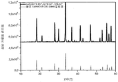
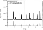
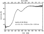
도 1a 는 참조 Lu3Al5O12 의 회절 패턴과 비교해 볼 때 조성 Lu3Al5O12: Mn4+(0.1%), Ca2 +(0.1%) 의 형광체들의 X-선 회절 패턴들의 비교를 나타낸다. X-선 회절 패턴들은 Cu-K-알파 방사를 사용하여 Rigaku Miniflux II 로 기록되었다. 측정 범위 2Θ 는 10°~ 60°이었다.
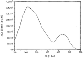
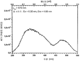
도 1b 는 Lu3Al5O12: Mn4 +(0.1%), Ca2 +(0.1%) 의 여기 스펙트럼을 나타낸다. 스펙트럼은 실온에서 Hamamatsu 광전자증배관 (photomultiplier) 및 Xe 고압 램프를 사용하여 Edinburgh Instruments FL920 분광기로 반무한 두께의 분말 층에 대해 기록되었다.
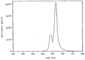
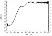
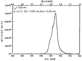
도 1c 는 Lu3Al5O12: Mn4 +(0.1%), Ca2 +(0.1%) 의 표준 방출 스펙트럼을 나타낸다. 스펙트럼은 실온에서 Hamamatsu 광전자증배관 및 Xe 고압 램프를 사용하여 Edinburgh Instruments FL920 분광기로 반무한 두께의 분말 층에 대해 기록되었다.
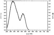
도 1d 는 Lu3Al5O12: Mn4 +(0.1%), Ca2 +(0.1%) 의 반사 스펙트럼을 나타낸다. 스펙트럼은 실온에서 Hamamatsu 광전자증배관 및 Xe 고압 램프를 사용하여 Ulbricht 구체 (sphere) 에서 Edinburgh Instruments FS920 분광기로 반무한 두께의 분말 층에 대해 기록되었다.
도 2a 는 참조 Lu3Al5O12 의 회절 패턴과 비교해 볼 때 조성 Lu3Al4.5Sc0.5O12:Mn(0.1%),Ca(0.1%) 의 형광체들의 X-선 회절 패턴들의 비교를 나타낸다. X-선 회절 패턴들은 Cu-K-알파 방사를 사용하여 Rigaku Miniflux II 로 기록되었다. 측정 범위 2Θ 는 10°~ 60°이었다.
도 2b 는 Lu3Al4 .5Sc0 .5O12:Mn(0.1%), Ca(0.1%) 의 여기 스펙트럼을 나타낸다. 스펙트럼은 실온에서 Hamamatsu 광전자증배관 및 Xe 고압 램프를 사용하여 Edinburgh Instruments FL920 분광기로 반무한 두께의 분말 층에 대해 기록되었다.
도 2c 는 Lu3Al4 .5Sc0 .5O12:Mn(0.1%), Ca(0.1%) 의 표준 방출 스펙트럼을 나타낸다. 스펙트럼은 실온에서 Hamamatsu 광전자증배관 및 Xe 고압 램프를 사용하여 Edinburgh Instruments FL920 분광기로 반무한 두께의 분말 층에 대해 기록되었다.
도 2d 는 Lu3Al4 .5Sc0 .5O12:Mn(0.1%), Ca(0.1%) 의 반사 스펙트럼을 나타낸다. 스펙트럼은 실온에서 Hamamatsu 광전자증배관 및 Xe 고압 램프를 사용하여 Ulbricht 구체에서 Edinburgh Instruments FS920 분광기로 반무한 두께의 분말 층에 대해 기록되었다.
도 3a 는 참조 Lu3Al5O12 의 회절 패턴과 비교해 볼 때 조성 (Lu0.5Y0.5)3Al5O12:Mn(0.1%), Ca(0.1%) 의 형광체들의 X-선 회절 패턴들의 비교를 나타낸다. X-선 회절 패턴들은 Cu-K-알파 방사를 사용하여 Rigaku Miniflux II 로 기록되었다. 측정 범위 2Θ 는 10°~ 60°이었다.
도 3b 는 (Lu0 .5Y0 .5)3Al5O12:Mn(0.1%), Ca(0.1%)의 여기 스펙트럼을 나타낸다. 스펙트럼은 실온에서 Hamamatsu 광전자증배관 및 Xe 고압 램프를 사용하여 Edinburgh Instruments FL920 분광기로 반무한 두께의 분말 층에 대해 기록되었다.
도 3c 는 (Lu0 .5Y0 .5)3Al5O12:Mn(0.1%), Ca(0.1%) 의 표준 방출 스펙트럼을 나타낸다. 스펙트럼은 실온에서 Hamamatsu 광전자증배관 및 Xe 고압 램프를 사용하여 Edinburgh Instruments FL920 분광기로 반무한 두께의 분말 층에 대해 기록되었다.
도 3d 는 (Lu0 .5Y0 .5)3Al5O12:Mn(0.1%), Ca(0.1%) 의 반사 스펙트럼을 나타낸다. 스펙트럼은 실온에서 Hamamatsu 광전자증배관 및 Xe 고압 램프를 사용하여 Ulbricht 구체에서 Edinburgh Instruments FS920 분광기로 반무한 두께의 분말 층에 대해 기록되었다.
도 4a 는 참조 Lu3Al5O12 의 회절 패턴과 비교해 볼 때 조성 (Lu0.5Gd0.5)3Al5O12:Mn(0.1%), Ca(0.1%) 의 형광체들의 X-선 회절 패턴들의 비교를 나타낸다. X-선 회절 패턴들은 Cu-K-알파 방사를 사용하여 Rigaku Miniflux II 로 기록되었다. 측정 범위 2Θ 는 10°~ 60°이었다.
도 4b 는 (Lu0 .5Gd0 .5)3Al5O12:Mn(0.1%), Ca(0.1%) 의 여기 스펙트럼을 나타낸다. 스펙트럼은 실온에서 Hamamatsu 광전자증배관 및 Xe 고압 램프를 사용하여 Edinburgh Instruments FL920 분광기로 반무한 두께의 분말 층에 대해 기록되었다.
도 4c 는 (Lu0 .5Gd0 .5)3Al5O12:Mn(0.1%), Ca(0.1%) 의 표준 방출 스펙트럼을 나타낸다. 스펙트럼은 실온에서 Hamamatsu 광전자증배관 및 Xe 고압 램프를 사용하여 Edinburgh Instruments FL920 분광기로 반무한 두께의 분말 층에 대해 기록되었다.
도 4d 는 (Lu0 .5Gd0 .5)3Al5O12:Mn(0.1%), Ca(0.1%) 의 반사 스펙트럼을 나타낸다. 스펙트럼은 실온에서 Hamamatsu 광전자증배관 및 Xe 고압 램프를 사용하여 Ulbricht 구체에서 Edinburgh Instruments FS920 분광기로 반무한 두께의 분말 층에 대해 기록되었다.As is common in laser physics, it should be noted that the phosphor compositions in the following sixteen figures are represented in each case by omitted notation. This is, for example, Lu 2 .995 .995 Al 4 O 12: Mn 0 .005 0 .005 Ca a "Lu 3 Al 5 O 12: Mn 4 + (0.1%), Ca 2+ (0.1%) ”means omitted.
1a shows the composition Lu 3 Al 5 O 12 : Mn 4+ (0.1%) when compared with the diffraction pattern of the reference Lu 3 Al 5 O 12 ; Ca 2 + shows a comparison of fluorescent X- ray diffraction pattern of a (0.1%). X-ray diffraction patterns were recorded with Rigaku Miniflux II using Cu-K-alpha radiation. The measurement range 2Θ was 10 ° to 60 °.
1b is Lu 3 Al 5 O 12 : Mn 4 + (0.1%), Ca 2 shows the excitation spectrum of + 0.1%. Spectra were recorded on a half-thick powder layer with an Edinburgh Instruments FL920 spectrometer at room temperature using a Hamamatsu photomultiplier and Xe high pressure lamp.
1c is Lu 3 Al 5 O 12 : Mn 4 + (0.1%), Ca 2 shows the emission spectrum of the standard + (0.1%). Spectra were recorded on a half-thick powder layer with an Edinburgh Instruments FL920 spectrometer at room temperature using a Hamamatsu photomultiplier tube and an Xe high pressure lamp.
1d shows Lu 3 Al 5 O 12 : Mn 4 + (0.1%), Ca 2 shows the reflection spectrum of + 0.1%. Spectra were recorded for half the thickness of the powder layer on an Edinburgh Instruments FS920 spectrometer in an Ulbricht sphere using a Hamamatsu photomultiplier tube and Xe high pressure lamp at room temperature.
2a shows a comparison of X-ray diffraction patterns of phosphors of composition Lu 3 Al 4.5 Sc 0.5 O 12 : Mn (0.1%), Ca (0.1%) as compared to the diffraction pattern of reference Lu 3 Al 5 O 12 . . X-ray diffraction patterns were recorded with Rigaku Miniflux II using Cu-K-alpha radiation. The measurement range 2Θ was 10 ° to 60 °.
Figure 2b Lu 3 Al 4 .5 Sc 0 .5 O 12: shows the excitation spectra of Mn (0.1%), Ca ( 0.1%). Spectra were recorded on a half-thick powder layer with an Edinburgh Instruments FL920 spectrometer at room temperature using a Hamamatsu photomultiplier tube and an Xe high pressure lamp.
Figure 2c Lu 3 Al 4 .5 Sc 0 .5 O 12: represents the standard emission spectra of Mn (0.1%), Ca ( 0.1%). Spectra were recorded on a half-thick powder layer with an Edinburgh Instruments FL920 spectrometer at room temperature using a Hamamatsu photomultiplier tube and an Xe high pressure lamp.
Figure 2d is Lu 3 Al 4 .5 Sc 0 .5 O 12: shows the reflection spectra of Mn (0.1%), Ca ( 0.1%). Spectra were recorded at room temperature on a half-thick powder layer with an Edinburgh Instruments FS920 spectrometer in an Ulbricht sphere using a Hamamatsu photomultiplier tube and an Xe high pressure lamp.
3A shows the X-ray diffraction patterns of phosphors of composition (Lu 0.5 Y 0.5 ) 3 Al 5 O 12 : Mn (0.1%), Ca (0.1%) as compared to the diffraction pattern of reference Lu 3 Al 5 O 12 . The comparison is shown. X-ray diffraction patterns were recorded with Rigaku Miniflux II using Cu-K-alpha radiation. The measurement range 2Θ was 10 ° to 60 °.
Figure 3b (Lu 0 .5 Y 0 .5) 3 Al 5 O 12: shows the excitation spectra of Mn (0.1%), Ca ( 0.1%). Spectra were recorded on a half-thick powder layer with an Edinburgh Instruments FL920 spectrometer at room temperature using a Hamamatsu photomultiplier tube and an Xe high pressure lamp.
Figure 3c (Lu 0 .5 Y 0 .5) 3 Al 5 O 12: represents the standard emission spectra of Mn (0.1%), Ca ( 0.1%). Spectra were recorded on a half-thick powder layer with an Edinburgh Instruments FL920 spectrometer at room temperature using a Hamamatsu photomultiplier tube and an Xe high pressure lamp.
Figure 3d (Lu 0 .5 Y 0 .5) 3 Al 5 O 12: shows the reflection spectra of Mn (0.1%), Ca ( 0.1%). Spectra were recorded at room temperature on a half-thick powder layer with an Edinburgh Instruments FS920 spectrometer in an Ulbricht sphere using a Hamamatsu photomultiplier tube and an Xe high pressure lamp.
4A shows the X-ray diffraction patterns of phosphors of composition (Lu 0.5 Gd 0.5 ) 3 Al 5 O 12 : Mn (0.1%), Ca (0.1%) as compared to the diffraction pattern of reference Lu 3 Al 5 O 12 . The comparison is shown. X-ray diffraction patterns were recorded with Rigaku Miniflux II using Cu-K-alpha radiation. The measurement range 2Θ was 10 ° to 60 °.
Figure 4b (Lu 0 .5 0 .5 Gd) 3 Al 5 O 12: it shows the excitation spectra of Mn (0.1%), Ca ( 0.1%). Spectra were recorded on a half-thick powder layer with an Edinburgh Instruments FL920 spectrometer at room temperature using a Hamamatsu photomultiplier tube and an Xe high pressure lamp.
Figure 4c (Lu 0 .5 0 .5 Gd) 3 Al 5 O 12: represents the standard emission spectra of Mn (0.1%), Ca ( 0.1%). Spectra were recorded on a half-thick powder layer with an Edinburgh Instruments FL920 spectrometer at room temperature using a Hamamatsu photomultiplier tube and an Xe high pressure lamp.
Figure 4d is (Lu 0 .5 0 .5 Gd) 3 Al 5 O 12: it shows the reflection spectra of Mn (0.1%), Ca ( 0.1%). Spectra were recorded at room temperature on a half-thick powder layer with an Edinburgh Instruments FS920 spectrometer in an Ulbricht sphere using a Hamamatsu photomultiplier tube and an Xe high pressure lamp.
예들Examples
예 1: Lu2 .995Al4 .995O12: Mn0 .005Ca0 . 005 의 제조Example 1: Lu 2 .995 Al 4 .995 O 12:
5.0125 g (0.0126 mol) 의 Y2O3, 0.0042g 의 CaCO3 (4.2115*10-5 mol) 및 0.0075g (4.2115*10-5 mol) 의 MnC2O4*2H2O 을 가온하면서 진한 HNO3 에 용해시킨다. 이 용액에 300 ml 의 물 내의 15.7827 g (0.0427 mol) 의 Al(NO3)3*9H2O 를 첨가하고, 후속하여 10g 의 시트르산을 첨가하고, 30 분간 교반을 실시한다. 용액을 150 ℃ 건조기 (drying cabinet) 내에서 하룻밤 동안 건조하고, 결과적인 시트레이트 전구체를 정교하게 연마한다. 분말을 1000 ℃ 에서 3 시간 동안 소성한 후 1750 ℃ 공기 중에서 5 시간 동안 소성하였다.Concentrated HNO while warming 5.0125 g (0.0126 mol) of Y 2 O 3 , 0.0042 g of CaCO 3 (4.2115 * 10 -5 mol) and 0.0075 g (4.2115 * 10 -5 mol) of MnC 2 O 4 * 2H 2 O Dissolve in 3 To this solution is added 15.7827 g (0.0427 mol) of Al (NO 3 ) 3 * 9H 2 O in 300 ml of water, followed by 10 g of citric acid, followed by stirring for 30 minutes. The solution is dried overnight in a 150 ° C. drying cabinet and the resulting citrate precursor is carefully polished. The powder was calcined at 1000 ° C. for 3 hours and then calcined at 1750 ° C. for 5 hours in air.
예 2: Lu2 .995Al4 .495Sc0 .5O12:Mn0 .005Ca0 . 005 의 제조Example 2: Lu 2 .995 Al 4 .495 Sc 0 .5 O 12:
5.0125 g 의 Lu2O3 및 0.5808 g 의 Sc2O3 을 가온하면서 진한 HNO3 에 용해시킨 후, 0.0042 g 의 CaCO3 을 첨가한다. 14.2028 의 Al(NO3)3*9H2O 및 0.0075 g 의 망간 옥살레이트를 증류수에 용해시켜, 전구체 용액에 첨가한다. 이 용액에 10 g 의 시트르산을 첨가하고, 가온하면서 30 분간 교반한다. 용액을 130 ℃ 건조기 내에서 하룻밤 동안 증발시키고, 결과적인 시트레이트 전구체를 정교하게 연마한다. 분말을 1000 ℃ 에서 3 시간 동안 소성한 후 1700 ℃ 공기 중에서 4 시간 동안 소성하였다.Was dissolved in concentrated HNO 3 and allowed to warm to 5.0125 g of Lu 2 O 3 and 0.5808 g of Sc 2 O 3, CaCO 3 is added to the 0.0042 g. 14.2028 Al (NO 3 ) 3 * 9H 2 O and 0.0075 g of manganese oxalate are dissolved in distilled water and added to the precursor solution. 10 g of citric acid is added to this solution and stirred for 30 minutes while warming. The solution is evaporated overnight in a 130 ° C. drier and the resulting citrate precursor is finely polished. The powder was calcined at 1000 ° C. for 3 hours and then calcined at 1700 ° C. for 4 hours in air.
예 3: Lu1 .4975Y1 .4975Al4 .995 O12:Mn0 .005Ca0 . 005 의 제조Example 3: Lu Y 1 .4975 1 .4975 .995 Al 4 O 12: Mn 0 .005 Ca 0. 005 Preparation
2.507 g 의 Lu2O3 및 1.4226 g 의 Y2O3 을 가온하면서 진한 HNO3 에 용해시키고, 4.2 mg 의 CaCO3 을 첨가한다. 15.783 g 의 Al(NO3)3*9H2O 및 7.5 mg 의 망간 옥살레이트를 증류수에 용해시켜, 전구체 용액에 첨가한다. 이 용액에 10 g 의 시트르산을 첨가하고, 가온하면서 30 분간 교반한다. 용액을 130 ℃ 건조기 내에서 하룻밤 동안 증발시키고, 결과적인 시트레이트 전구체를 연마한다. 분말을 1000 ℃ 에서 3 시간 동안 소성한 후 1700 ℃ 공기 중에서 4 시간 동안 소성하였다.And allowed to warm to 2.507 g of Lu 2 O 3 and Y 2 O 3 of 1.4226 g was dissolved in concentrated HNO 3 and, the addition of CaCO 3 in the 4.2 mg. 15.783 g of Al (NO 3 ) 3 * 9H 2 O and 7.5 mg of manganese oxalate are dissolved in distilled water and added to the precursor solution. 10 g of citric acid is added to this solution and stirred for 30 minutes while warming. The solution is evaporated overnight in a 130 ° C. drier and the resulting citrate precursor is polished. The powder was calcined at 1000 ° C. for 3 hours and then calcined at 1700 ° C. for 4 hours in air.
예 4 : Lu1 .4975Gd1 .4975Al4 .995O12:Mn0 .005Ca0 . 005 의 제조Example 4: Gd Lu 1 .4975 1 .4975 .995 Al 4 O 12: Mn 0 .005 Ca 0. 005 Preparation
23.507 g 의 Lu2O3 및 2.284 g 의 Gd2O3 을 가온하면서 진한 HNO3 에 용해킨 후, 이 용액에 4.2 mg 의 CaCO3 을 첨가한다. 15.783 g 의 Al(NO3)3*9H2O 및 7.5 mg 의 망간 옥살레이트를 증류수에 용해시켜, 전구체 용액에 첨가한다. 이 용액에 10 g 의 시트르산을 첨가하고, 가온하면서 30 분간 교반한다. 용액을 130 ℃ 건조기 내에서 하룻밤 동안 증발시키고, 결과적인 시트레이트 전구체를 연마한다. 분말을 1000 ℃ 에서 3 시간 동안 소성한 후 1700 ℃ 공기 중에서 4 시간 동안 소성하였다.23.507 g Lu 2 O 3 and 2.284 g Gd 2 O 3 dissolved in concentrated HNO 3 with warming Thereafter, 4.2 mg of CaCO 3 is added to this solution. 15.783 g of Al (NO 3 ) 3 * 9H 2 O and 7.5 mg of manganese oxalate are dissolved in distilled water and added to the precursor solution. 10 g of citric acid is added to this solution and stirred for 30 minutes while warming. The solution is evaporated overnight in a 130 ° C. drier and the resulting citrate precursor is polished. The powder was calcined at 1000 ° C. for 3 hours and then calcined at 1700 ° C. for 4 hours in air.
예 5 : 발광 다이오드의 제조Example 5: Fabrication of Light Emitting Diodes
텀블 믹서 (tumble mixer) 내에서 예 1 내지 예 4 로부터의 형광체와 2-성분 실리콘 (Dow Corning 으로부터의 OE6550) 을, 동일량의 형광체가 2 성분의 실리콘 내에 분산되도록 혼합하여, 실리콘 내의 형광체 혼합물의 전체 농도가 8 중량% 가 되게 한다.In a tumble mixer, the phosphors from Examples 1 to 4 and two-component silicon (OE6550 from Dow Corning) are mixed so that the same amount of phosphor is dispersed in the two-component silicon, so as to The total concentration is 8% by weight.
2종의 형광체-함유 실리콘 성분들 각각 5 ㎖ 를 서로 균질하게 혼합하고, 디스펜서로 이송한다. 100 ㎛2 GaN 칩을 포함하는, OSA optoelectronics, Berlin 로부터의 빈 LED 패키지들을 디스펜서의 도움으로 채운다. 그 후, LED들을 가열 챔버 내에 배치하여 150 ℃ 에서 1 시간 동안 실리콘을 고형화한다.5 ml of each of the two phosphor-containing silicone components are mixed homogeneously with each other and transferred to a dispenser. Empty LED packages from OSA optoelectronics, Berlin, including a 100 μm 2 GaN chip, are filled with the help of a dispenser. The LEDs are then placed in a heating chamber to solidify the silicon at 150 ° C. for 1 hour.

표 1 은 본 발명에 따른 형광체들의 광학 성질들을 나타낸다.Table 1 shows the optical properties of the phosphors according to the invention.
CIE x 및 CIE y 는 당업자에게 친숙한 표준 CIE 컬러 차트 (여기서 표준 관측자 1931) 에서의 좌표들을 나타내며, 이것에 의해 광원의 컬러가 기술된다. 상기 언급된 모든 양들은 당업자에게 친숙한 방법들에 의해 광원의 방출 스펙트럼으로부터 계산된다.CIE x and CIE y represent coordinates in a standard CIE color chart (here standard observer 1931) that is familiar to those skilled in the art, whereby the color of the light source is described. All the amounts mentioned above are calculated from the emission spectrum of the light source by methods familiar to those skilled in the art.
Claims (12)
여기서
A 는 Y, Gd 또는 Tb 를 나타내고,
x 는 0 내지 2.90 범위의 값을 나타내고,
y 는 0 내지 0.50 범위의 값을 나타내고,
z 는 0.005 내지 0.05 범위의 값을 나타내는, 화합물.As a compound of Formula I
here
A represents Y, Gd or Tb,
x represents a value ranging from 0 to 2.90,
y represents a value ranging from 0 to 0.50,
z represents a value ranging from 0.005 to 0.05.
x 는 0 내지 2.0 범위의 값을 나타내고, 바람직하게는 0.10 내지 0.90 범위의 값을 나타내는 것을 특징으로 하는 화합물.The method of claim 1,
x represents a value in the range from 0 to 2.0, preferably a value in the range from 0.10 to 0.90.
y 는 0.10 내지 0.45 범위의 값을 나타내고, 바람직하게는 0.20 내지 0.40 범위의 값을 나타내는 것을 특징으로 하는 화합물.The method according to claim 1 or 2,
y represents a value in the range of 0.10 to 0.45, preferably a value in the range of 0.20 to 0.40.
a) 루테튬-, 스칸듐-, 칼슘-, 알루미늄-, 망간-, 이트륨-, 테르븀- 및/또는 가돌리늄-함유 재료들의 혼합 공정 단계,
b) 적어도 하나의 추가적인 무기 물질 및/또는 유기 물질의 첨가 공정 단계, 및
c) 상기 혼합물의 열처리 공정 단계를 포함하는, 화합물의 제조 방법.As a manufacturing method of the compound in any one of Claims 1-3,
a) mixing process steps of lutetium-, scandium-, calcium-, aluminum-, manganese-, yttrium-, terbium- and / or gadolinium-containing materials,
b) addition process step of at least one additional inorganic material and / or organic material, and
c) a heat treatment process step of the mixture.
상기 무기 물질 또는 유기 물질 (공정 단계 b) 은, 암모늄 할로겐화물들, 알칼리 토류 금속 불화물들 (이를 테면 칼슘 불화물, 스트론튬 불화물 또는 바륨 불화물), 알칼리 토류 또는 알칼리 금속 보레이트류, 붕산, 알칼리 토류 또는 알칼리 금속 카보네이트류 또는 암모늄 탄산수소염, 시트르산, 알코올레이트류, 그리고 옥살레이트류 및/또는 실리케이트류 (예를 들면 TEOS) 의 그룹으로부터 선택되는 것을 특징으로 하는 화합물의 제조 방법.5. The method of claim 4,
The inorganic or organic material (process step b) may be selected from ammonium halides, alkaline earth metal fluorides (such as calcium fluoride, strontium fluoride or barium fluoride), alkaline earth or alkali metal borates, boric acid, alkaline earth or alkali A method for producing a compound, characterized in that it is selected from the group of metal carbonates or ammonium bicarbonate, citric acid, alcoholates, and oxalates and / or silicates (eg TEOS).
상기 혼합물의 열처리는 복수의 단계들로 실시되며, 바람직하게는 2개의 단계들로 실시되는 것을 특징으로 하는 화합물의 제조 방법.The method according to claim 4 or 5,
The heat treatment of the mixture is carried out in a plurality of steps, preferably in two steps.
제 1 항 내지 제 3 항 중 어느 한 항에 기재된 식 I 의 적어도 하나의 화합물을 포함하는 것을 특징으로 하는 광원.semiconductor; And
A light source comprising at least one compound of formula I according to any one of claims 1 to 3.
상기 반도체는 발광 인듐 알루미늄 갈륨 질화물이고, 특히 식 IniGajAlkN (여기서 0≤i, 0≤j, 0≤k, 그리고 i+j+k=1) 의 발광 인듐 알루미늄 갈륨 질화물인 것을 특징으로 하는 광원.The method of claim 7, wherein
The semiconductor is a light emitting indium aluminum gallium nitride, in particular a light emitting indium aluminum gallium nitride of the formula In i Ga j Al k N (where 0 ≦ i, 0 ≦ j, 0 ≦ k, and i + j + k = 1). Characterized by light source.
상기 반도체와 형광체 (phosphor) 사이의 광학 커플링이 광전도 장치 (light-conducting arrangement) 에 의해 실현되는 것을 특징으로 하는 조명 유닛.The method of claim 9,
Optical coupling between the semiconductor and phosphor is realized by a light-conducting arrangement.
Applications Claiming Priority (3)
| Application Number | Priority Date | Filing Date | Title |
|---|---|---|---|
| DE102010047474A DE102010047474A1 (en) | 2010-10-06 | 2010-10-06 | Mn-activated phosphors |
| DE102010047474.6 | 2010-10-06 | ||
| PCT/EP2011/004652 WO2012045393A1 (en) | 2010-10-06 | 2011-09-16 | Mn-activated phosphors |
Publications (1)
| Publication Number | Publication Date |
|---|---|
| KR20130111562A true KR20130111562A (en) | 2013-10-10 |
Family
ID=44677842
Family Applications (1)
| Application Number | Title | Priority Date | Filing Date |
|---|---|---|---|
| KR1020137011771A KR20130111562A (en) | 2010-10-06 | 2011-09-16 | Mn-activated phosphors |
Country Status (7)
| Country | Link |
|---|---|
| US (1) | US9080104B2 (en) |
| EP (1) | EP2625247B1 (en) |
| JP (1) | JP5912121B2 (en) |
| KR (1) | KR20130111562A (en) |
| CN (1) | CN103154196A (en) |
| DE (1) | DE102010047474A1 (en) |
| WO (1) | WO2012045393A1 (en) |
Families Citing this family (6)
| Publication number | Priority date | Publication date | Assignee | Title |
|---|---|---|---|---|
| JP2016524630A (en) * | 2013-05-02 | 2016-08-18 | メルク パテント ゲゼルシャフト ミット ベシュレンクテル ハフツングMerck Patent Gesellschaft mit beschraenkter Haftung | Phosphor |
| KR102355081B1 (en) | 2014-12-26 | 2022-01-26 | 삼성전자주식회사 | Method of manufacturing fluoride phosphor, light emitting device, display apparatus and illumination apparatus |
| MX2017015998A (en) | 2015-06-29 | 2018-04-20 | Dow Global Technologies Llc | Process for producing flexible container with microcapillary dispensing system. |
| CN105331364B (en) * | 2015-10-12 | 2017-09-05 | 杭州电子科技大学 | A kind of YAG:Mn red fluorescence powders with and its preparation method and application |
| DE102015015355A1 (en) | 2015-12-01 | 2017-06-01 | Merck Patent Gmbh | Mn-activated phosphors |
| KR102419770B1 (en) * | 2016-05-20 | 2022-07-13 | 가부시키가이샤 한도오따이 에네루기 켄큐쇼 | Light-emitting device and electronic device |
Family Cites Families (15)
| Publication number | Priority date | Publication date | Assignee | Title |
|---|---|---|---|---|
| US4019884A (en) | 1976-01-22 | 1977-04-26 | Corning Glass Works | Method for providing porous broad-band antireflective surface layers on chemically-durable borosilicate glasses |
| NL181063C (en) * | 1976-05-13 | 1987-06-01 | Philips Nv | LUMINESCENT SCREEN; LOW-PRESSURE MERCURY DISCHARGE LAMP; PROCESS FOR PREPARING A LUMINESCENT MATERIAL |
| NL7700419A (en) * | 1977-01-17 | 1978-07-19 | Philips Nv | MAGNETIC BUBBLE DOMAIN MATERIAL. |
| JP3242561B2 (en) | 1995-09-14 | 2001-12-25 | メルク・ジヤパン株式会社 | Flaky aluminum oxide, pearlescent pigment and method for producing the same |
| US6556336B2 (en) * | 1997-07-24 | 2003-04-29 | Scientific Materials, Corp. | Optical laser light limiter |
| DE29820384U1 (en) * | 1998-11-06 | 1999-01-14 | Opto System Gmbh | Luminous or display element with mixed-colored, especially white light |
| TW593188B (en) | 2001-09-21 | 2004-06-21 | Merck Patent Gmbh | Hybrid sol for the production of abrasion-resistant SiO2 antireflection layers |
| DE10213294B4 (en) | 2002-03-25 | 2015-05-13 | Osram Gmbh | Use of a UV-resistant polymer in optoelectronics and outdoor applications, UV-resistant polymer and optical component |
| CN1255506C (en) * | 2003-11-13 | 2006-05-10 | 北京有色金属研究总院 | Boron-containing luminescent powder for LED, preparing method thereof and electric light source therefrom |
| DE102006027306B4 (en) * | 2006-06-06 | 2013-10-17 | Schott Ag | Process for the preparation of a glass ceramic with a garnet phase and use of the glass ceramic produced thereafter |
| DE102006027133A1 (en) | 2006-06-12 | 2007-12-13 | Merck Patent Gmbh | Process for the preparation of garnet phosphors in a pulsation reactor |
| DE102006037730A1 (en) | 2006-08-11 | 2008-02-14 | Merck Patent Gmbh | LED conversion phosphors in the form of ceramic bodies |
| DE102006054331A1 (en) | 2006-11-17 | 2008-05-21 | Merck Patent Gmbh | Phosphor body based on platelet-shaped substrates |
| US9133392B2 (en) * | 2010-07-22 | 2015-09-15 | Osram Opto Semiconductors Gmbh | Garnet material, method for its manufacturing and radiation-emitting component comprising the garnet material |
| TWI486254B (en) * | 2010-09-20 | 2015-06-01 | Nitto Denko Corp | Light emissive ceramic laminate and method of making same |
-
2010
- 2010-10-06 DE DE102010047474A patent/DE102010047474A1/en not_active Withdrawn
-
2011
- 2011-09-16 KR KR1020137011771A patent/KR20130111562A/en active IP Right Grant
- 2011-09-16 WO PCT/EP2011/004652 patent/WO2012045393A1/en active Application Filing
- 2011-09-16 EP EP11761009.7A patent/EP2625247B1/en not_active Not-in-force
- 2011-09-16 JP JP2013532060A patent/JP5912121B2/en not_active Expired - Fee Related
- 2011-09-16 CN CN2011800481843A patent/CN103154196A/en active Pending
- 2011-09-16 US US13/877,954 patent/US9080104B2/en not_active Expired - Fee Related
Also Published As
| Publication number | Publication date |
|---|---|
| CN103154196A (en) | 2013-06-12 |
| JP5912121B2 (en) | 2016-04-27 |
| US9080104B2 (en) | 2015-07-14 |
| EP2625247B1 (en) | 2016-11-30 |
| JP2014502243A (en) | 2014-01-30 |
| WO2012045393A1 (en) | 2012-04-12 |
| DE102010047474A1 (en) | 2012-04-12 |
| EP2625247A1 (en) | 2013-08-14 |
| US20130193472A1 (en) | 2013-08-01 |
Similar Documents
| Publication | Publication Date | Title |
|---|---|---|
| US8987687B2 (en) | Silicophosphate phosphors | |
| JP5611960B2 (en) | Doped garnet phosphor with red shift for pcLED | |
| US8088304B2 (en) | Luminophores made of doped garnet for pcLEDs | |
| US20130063926A1 (en) | Phosphors | |
| US20100194263A1 (en) | Method for Producing Illuminants Based on Orthosilicates for pcLEDs | |
| US20100201250A1 (en) | METHOD OF PRODUCING ILLUMINANTS CONSISTING OF ORTHOSILICATES FOR pcLEDs | |
| JP6243438B2 (en) | EU-activated luminescent material | |
| JP2012519216A (en) | Nitridosilicate co-doped with zirconium and hafnium | |
| US20130120964A1 (en) | Aluminate phosphors | |
| US9080104B2 (en) | Mn-activated phosphors | |
| JP2012509238A (en) | Co-doped 1-1-2 nitride | |
| KR101752939B1 (en) | Sm-activated aluminate and borate phosphors | |
| TWI551667B (en) | Carbodiimide phosphors |
Legal Events
| Date | Code | Title | Description |
|---|---|---|---|
| A201 | Request for examination | ||
| E902 | Notification of reason for refusal | ||
| E701 | Decision to grant or registration of patent right |