KR20130107199A - Phase change memory array blocks with alternate selection - Google Patents
Phase change memory array blocks with alternate selection Download PDFInfo
- Publication number
- KR20130107199A KR20130107199A KR1020127031016A KR20127031016A KR20130107199A KR 20130107199 A KR20130107199 A KR 20130107199A KR 1020127031016 A KR1020127031016 A KR 1020127031016A KR 20127031016 A KR20127031016 A KR 20127031016A KR 20130107199 A KR20130107199 A KR 20130107199A
- Authority
- KR
- South Korea
- Prior art keywords
- cells
- block
- pcm
- memory
- memory location
- Prior art date
Links
Images


Classifications
-
- G—PHYSICS
- G11—INFORMATION STORAGE
- G11C—STATIC STORES
- G11C13/00—Digital stores characterised by the use of storage elements not covered by groups G11C11/00, G11C23/00, or G11C25/00
- G11C13/02—Digital stores characterised by the use of storage elements not covered by groups G11C11/00, G11C23/00, or G11C25/00 using elements whose operation depends upon chemical change
-
- G—PHYSICS
- G11—INFORMATION STORAGE
- G11C—STATIC STORES
- G11C13/00—Digital stores characterised by the use of storage elements not covered by groups G11C11/00, G11C23/00, or G11C25/00
- G11C13/0002—Digital stores characterised by the use of storage elements not covered by groups G11C11/00, G11C23/00, or G11C25/00 using resistive RAM [RRAM] elements
- G11C13/0021—Auxiliary circuits
- G11C13/0023—Address circuits or decoders
- G11C13/0028—Word-line or row circuits
-
- G—PHYSICS
- G11—INFORMATION STORAGE
- G11C—STATIC STORES
- G11C13/00—Digital stores characterised by the use of storage elements not covered by groups G11C11/00, G11C23/00, or G11C25/00
- G11C13/0002—Digital stores characterised by the use of storage elements not covered by groups G11C11/00, G11C23/00, or G11C25/00 using resistive RAM [RRAM] elements
- G11C13/0004—Digital stores characterised by the use of storage elements not covered by groups G11C11/00, G11C23/00, or G11C25/00 using resistive RAM [RRAM] elements comprising amorphous/crystalline phase transition cells
-
- G—PHYSICS
- G11—INFORMATION STORAGE
- G11C—STATIC STORES
- G11C13/00—Digital stores characterised by the use of storage elements not covered by groups G11C11/00, G11C23/00, or G11C25/00
- G11C13/0002—Digital stores characterised by the use of storage elements not covered by groups G11C11/00, G11C23/00, or G11C25/00 using resistive RAM [RRAM] elements
- G11C13/0021—Auxiliary circuits
- G11C13/0023—Address circuits or decoders
- G11C13/0026—Bit-line or column circuits
-
- G—PHYSICS
- G11—INFORMATION STORAGE
- G11C—STATIC STORES
- G11C13/00—Digital stores characterised by the use of storage elements not covered by groups G11C11/00, G11C23/00, or G11C25/00
- G11C13/0002—Digital stores characterised by the use of storage elements not covered by groups G11C11/00, G11C23/00, or G11C25/00 using resistive RAM [RRAM] elements
- G11C13/0021—Auxiliary circuits
- G11C13/0033—Disturbance prevention or evaluation; Refreshing of disturbed memory data
-
- G—PHYSICS
- G11—INFORMATION STORAGE
- G11C—STATIC STORES
- G11C13/00—Digital stores characterised by the use of storage elements not covered by groups G11C11/00, G11C23/00, or G11C25/00
- G11C13/0002—Digital stores characterised by the use of storage elements not covered by groups G11C11/00, G11C23/00, or G11C25/00 using resistive RAM [RRAM] elements
- G11C13/0021—Auxiliary circuits
- G11C13/0069—Writing or programming circuits or methods
- G11C2013/0088—Write with the simultaneous writing of a plurality of cells
-
- G—PHYSICS
- G11—INFORMATION STORAGE
- G11C—STATIC STORES
- G11C2213/00—Indexing scheme relating to G11C13/00 for features not covered by this group
- G11C2213/70—Resistive array aspects
- G11C2213/72—Array wherein the access device being a diode
-
- G—PHYSICS
- G11—INFORMATION STORAGE
- G11C—STATIC STORES
- G11C8/00—Arrangements for selecting an address in a digital store
- G11C8/12—Group selection circuits, e.g. for memory block selection, chip selection, array selection
Abstract
상변화 메모리가 개시된다. 상변화 메모리는 복수의 블록 유닛을 갖는다. 블록 유닛은 교번하여 선택된다. 교번 블록 유닛 선택은 서브-워드라인 상에서 바운싱하고 서브-워드라인 드라이버 트랜지스터를 통해 그라운드 라인에 연결되는 피크 전류를 억제한다. 교번 비트라인 선택은 선택된 블록 유닛의 인접한 셀 히팅(heating) 간섭을 회피한다.Phase change memory is disclosed. The phase change memory has a plurality of block units. Block units are selected alternately. Alternating block unit selection suppresses peak currents that are bounded on the sub-wordline and connected to the ground line through the sub-wordline driver transistors. Alternate bitline selection avoids adjacent cell heating interference of the selected block unit.

Description
[관련 출원][Related Application]
본 출원은 2010년 4월 27일자 미국 가 특허 출원 제 61/328,421 호의 이익을 주장하며, 이것은 참조에 의해 그 전체가 본 명세서에 통합된다.This application claims the benefit of US Patent Application No. 61 / 328,421 to April 27, 2010, which is incorporated herein by reference in its entirety.
본 발명은 일반적으로 반도체 메모리에 관한 것이다. 더욱 구체적으로, 본 발명은 상변화 메모리에 관한 것이다.The present invention relates generally to semiconductor memories. More specifically, the present invention relates to a phase change memory.
상변화 메모리 장치의 적어도 한 형태 - PRAM(Phase-chage Random Access Memory: 상 변화 랜덤 액세스 메모리) - 는 논리 '1'을 나타내기 위해 비정질 상태를 사용하고 논리 '0'을 나타내기 위해 결정 상태를 사용한다. PRAM 장치에서, 결정 상태는 "세트 상태"로 불리고 비정질 상태는 "리세트 상태"로 불린다. 따라서, PRAM의 메모리 셀은 메모리 셀의 상변화 물질을 결정 상태로 설정함으로써 논리 '0'을 저장하고, 메모리 셀은 상변화 물질을 비정질 상태로 설정함으로써 논리 '1'을 저장한다.At least one type of phase change memory device, phase-chage random access memory (PRAM), uses an amorphous state to represent a logic '1' and a decision state to represent a logic '0'. use. In a PRAM device, the crystalline state is called "set state" and the amorphous state is called "reset state". Thus, the memory cell of the PRAM stores logic '0' by setting the phase change material of the memory cell to the crystalline state, and the memory cell stores the logic '1' by setting the phase change material to the amorphous state.
PRAM의 상변화 물질은, 미리 결정된 용융 온도보다 높은 제 1 온도로 물질을 가열하고, 이어서 이 물질을 급속 냉각함으로써 비정질 상태로 전이된다. 상변화 물질은 용융 온도보다 낮지만 결정화 온도보다 높은 제 2 온도에서 지속 기간 동안 이 물질을 가열함으로써 결정 상태로 전이된다. 따라서, 상기 기재된 바와 같이 가열 및 냉각을 사용하여 비정질 상태와 결정 상태 사이에서 PRAM의 메모리 셀의 상변화 물질을 전이시켜서, 데이터를 PRAM의 메모리 셀에 프로그래밍한다. The phase change material of the PRAM is transferred to an amorphous state by heating the material to a first temperature above a predetermined melting temperature and then rapidly cooling the material. The phase change material transitions to the crystalline state by heating the material for a duration at a second temperature below the melting temperature but above the crystallization temperature. Thus, heating and cooling are used to transfer the phase change material of the memory cell of the PRAM between the amorphous state and the crystalline state as described above, thereby programming the data into the memory cell of the PRAM.
전형적으로, PRAM의 상변화 물질은 게르마늄(Ge), 안티몬(Sb) 및 텔루륨(Te)을 포함한 화합물, 즉, "GST" 화합물을 포함한다. 가열과 냉각에 의한 비정질 상태와 결정 상태 사이의 빠른 전이가 가능하므로, GST 화합물은 PRAM에 아주 적합하다. GST 화합물에 추가하거나 그 대안으로서, 다양한 다른 화합물이 상변화 물질에서 사용될 수 있다. 다른 화합물의 예시는 GaSb, InSb, InSe, Sb2Te3 및 GeTe와 같은 2 원소 화합물, GeSbTe, GaSeTe, InSbTe, SnSb2Te4 및 InSbGe와 같은 3 원소 화합물 또는 AgInSbTe, (GeSn)SbTe, GeSb(SeTe) 및 Te81Ge15Sb2S2와 같은 4 원소 화합물을 포함하나 이에 한정되지 않는다.Typically, the phase change material of a PRAM includes compounds including germanium (Ge), antimony (Sb) and tellurium (Te), ie, "GST" compounds. GST compounds are well suited for PRAM because of the rapid transition between the amorphous and crystalline states by heating and cooling. In addition to or as an alternative to GST compounds, various other compounds may be used in the phase change material. Examples of other compounds include two-element compounds such as GaSb, InSb, InSe, Sb2Te3 and GeTe, three-element compounds such as GeSbTe, GaSeTe, InSbTe, SnSb2Te4 and InSbGe or AgInSbTe, (GeSn) SbTe, GeSb (SeTe) and Te2Ge; Including but not limited to quaternary compounds.
PRAM의 메모리 셀은 "상변화 메모리 셀"로 불린다. 상변화 메모리 셀은 일반적으로 상부 전극, 상변화 물질 층, 하부 전극 콘택, 하부 전극 및 액세스 트랜지스터를 포함한다. 판독 동작은 상변화 물질 층의 저항을 측정함으로써 상변화 메모리 셀 상에서 수행되고, 프로그램 동작은 상기 기재된 바와 같이 상변화 물질 층을 가열 및 냉각하여 상변화 메모리 셀 상에서 수행된다.The memory cells of the PRAM are called "phase change memory cells." Phase change memory cells generally include an upper electrode, a phase change material layer, a lower electrode contact, a lower electrode, and an access transistor. The read operation is performed on the phase change memory cell by measuring the resistance of the phase change material layer, and the program operation is performed on the phase change memory cell by heating and cooling the phase change material layer as described above.
상변화 메모리 장치는 전형적으로 메모리 셀 어레이, 기록 드라이버 회로, 및 열 선택 회로를 포함한다. 메모리 셀 어레이는 복수의 블록 유닛 및 복수의 워드라인 드라이버를 포함한다. 복수의 블록 유닛 각각은 복수의 워드라인 드라이버 중에서 한 쌍의 인접한 워드라인 드라이버들 사이에 연결되고 복수의 메모리 블록을 포함한다. 기록 드라이버 회로는 복수의 기록 드라이버 유닛을 포함한다. 기록 드라이버 유닛의 각각은, 개별 프로그래밍 전류를 복수의 블록 유닛 중에서 해당 블록 유닛에 제공하도록 적응된 복수의 기록 드라이버를 포함한다. 열 선택 회로는, 메모리 셀 어레이와 기록 드라이버 회로 사이에 연결되고 열 선택 신호에 응답하여 복수의 메모리 블록 중 적어도 하나를 선택하도록 적응되어서 복수의 메모리 블록 중 적어도 하나에 해당 프로그래밍 전류를 제공한다.Phase change memory devices typically include a memory cell array, a write driver circuit, and a column select circuit. The memory cell array includes a plurality of block units and a plurality of wordline drivers. Each of the plurality of block units is connected between a pair of adjacent word line drivers among the plurality of word line drivers and includes a plurality of memory blocks. The write driver circuit includes a plurality of write driver units. Each of the write driver units includes a plurality of write drivers adapted to provide individual programming currents to the corresponding block unit among the plurality of block units. The column select circuit is connected between the memory cell array and the write driver circuit and is adapted to select at least one of the plurality of memory blocks in response to the column select signal to provide a corresponding programming current to at least one of the plurality of memory blocks.
도 1a는 MOS 트랜지스터를 이용하는 상변화 메모리 셀의 예시를 도시한다. 도 1a에 따르면, 메모리 셀(10)은 GST 화합물과 네거티브 금속 산화물 반도체(NMOS) 트랜지스터(12; 또한 "NT"로도 표기됨)를 포함하는 상변화 저항 소자(11; 또한, GST로도 표기됨)를 포함한다. 상변화 저항 소자(11)는 비트라인(B/L)과 NMOS 트랜지스터(12) 사이에 연결된다. NMOS 트랜지스터(12)는 상변화 저항 소자(11)와 그라운드 사이에 연결된다. 게다가, NMOS 트랜지스터(12)는 워드라인(W/L)에 연결된 게이트를 갖는다. 1A shows an example of a phase change memory cell using a MOS transistor. According to FIG. 1A, the
NMOS 트랜지스터(12)는 워드라인(W/L)에 인가된 워드라인 전압에 응답하여 턴온된다. NMOS 트랜지스터(12)가 턴온되면, 상변화 저항 소자(11)는 비트라인(B/L)을 통해 전류를 수신한다. 도 1a에 도시된 특정 실시예에서, 상변화 저항 소자(11)는 비트라인(B/L)과 NMOS 트랜지스터(12) 사이에 연결되고, 대안적으로, 상변화 저항 소자(11)는 NMOS 트랜지스터(12)와 그라운드 사이에 연결될 수 있다.The
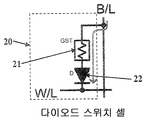
도 1b는 다이오드 형 상변화 메모리 셀의 예시를 도시한다. 도 1b에 따르면, 메모리 셀(20)은 비트라인(B/L)에 연결된 상변화 저항 소자(21; "GST"로도 표기됨), 및 상변화 저항 소자(21)와 워드라인(W/L) 사이에 연결된 다이오드(22; "D"로도 표기됨)를 포함한다. 상변화 메모리 셀(20)은 워드라인(W/L)과 비트라인(B/L)을 선택함으로써 선택된다. 상변화 메모리 셀(20)이 올바르게 작동하기 위해, 워드라인(W/L)이 선택되면 워드라인(W/L)은 비트라인(B/L)보다 더 낮은 전압 레벨을 가져야 하며(이것이 순방향 바이어스 상태임), 그에 따라 전류는 상변화 저항 소자(21)를 통해 흐를 수 있다. 워드라인(W/L)이 비트라인(B/L)보다 더 높은 전압을 가질 경우, 다이오드(22)는 역방향 바이어스되고, 상변화 메모리 저항 소자(21)를 통해서 전류가 흐르지 않는다. 워드라인(W/L)이 비트라인(B/L)보다 더 낮은 전압 레벨을 가지는 것을 보장하기 위해, 워드라인(W/L)이 선택되면 이것은 일반적으로 그라운드에 연결된다.1B shows an example of a diode phase change memory cell. According to FIG. 1B, the
도 1a 및 도 1b에서, 상변화 저항 소자(11, 21)는 대안적으로 광의의 의미에서 "메모리 소자"로 불릴 수 있으며 NMOS 트랜지스터(12) 및 다이오드(22)는 대안적으로 광의의 의미에서 "선택 소자"로 불릴 수 있다.1A and 1B, the phase
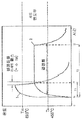
상변화 메모리 셀(10, 20)의 동작이 도 2를 참조하여 이하에서 기재된다. 특히, 도 2는 메모리 셀(10, 20)의 프로그래밍 동작 동안 상변화 저항 소자(11, 21)의 온도 특성을 도시하는 그래프이다. 도 2에서, 참조 번호(1)는 비정질 상태로의 전이 동안 상변화 저항 소자(11, 21)의 온도 특성을 표시하고, 참조 번호(2)는 결정 상태로의 전이 동안 상변화 저항 소자(11, 21)의 온도 특성을 표시한다.Operation of the phase
비정질 상태로의 전이에서, 용융 온도(Tm)보다 높게 GST 화합물의 온도를 증가시키기 위해, 기간(T1) 동안 상변화 저항 소자(11, 21)의 GST 화합물에 전류가 인가된다. 기간(T1) 이후, GST 화합물의 온도는 급격히 감소하거나, 또는 "?칭"되고(quenched), GST 화합물은 비정질 상태를 취한다. 반대로, 결정 상태로의 전이에서, 결정화 온도(Tx)보다 높게 GST 화합물의 온도를 증가시키기 위해, 기간 T2>T1) 동안 상변화 저항 소자(11, 21)의 GST 화합물에 전류가 인가된다. 지속기간(T2) 이후, GST 화합물은 결정화 온도 이하로 서서히 냉각되어서 결정 상태를 취한다. 도시된 예시에서, t1은 고온에서 저온으로의 온도 변화의 중간 지점이다. 예컨대, T1은 약 50ns가 될 수 있고 T2는 약 200ns가 될 수 있으나, 이것은 PCM 셀 구현에 따라 변화할 수 있다.In the transition to the amorphous state, a current is applied to the GST compounds of the phase
상변화 메모리 장치는 전형적으로 메모리 셀 어레이에 배열된 복수의 상변화 메모리 셀을 포함한다. 메모리 셀 어레이 내에서, 메모리 셀의 각각은 전형적으로 해당 비트라인 및 해당 워드라인에 연결된다. 예컨대, 메모리 셀 어레이는 열로 배열된 비트라인과 행으로 배열된 워드라인을 포함할 수 있으며, 상변화 메모리 셀은 열과 행 사이의 각 교차점 가까이에 위치한다. Phase change memory devices typically include a plurality of phase change memory cells arranged in a memory cell array. Within a memory cell array, each of the memory cells is typically connected to a corresponding bit line and a corresponding word line. For example, the memory cell array may include bit lines arranged in columns and word lines arranged in rows, and the phase change memory cells are located near each intersection point between the columns and the rows.
일반적으로, 특정 워드라인에 연결된 상변화 메모리 셀의 행은 특정 워드라인에 적절한 전압 레벨을 인가함으로써 선택된다. 예컨대, 도 1a에 도시된 바와 같은 상변화 메모리 셀(10)과 유사한 상변화 메모리 셀의 행을 선택하기 위하여, 비교적 높은 전압 레벨이 해당 워드라인(W/L)에 인가되어서 NMOS 트랜지스터(12)를 턴온한다. 대안적으로, 도 1b에 도시된 바와 같은 상변화 메모리 셀(20)과 유사한 상변화 메모리 셀의 행을 선택하기 위하여, 비교적 낮은 전압 레벨이 해당 워드라인(W/L)에 인가되어서 전류가 다이오드(22)를 통해 흐를 수 있다.In general, a row of phase change memory cells connected to a particular word line is selected by applying an appropriate voltage level to the particular word line. For example, to select a row of phase change memory cells similar to the phase
도 3은 모든 IO 동작에 대한 하나의 셀 어레이 선택을 도시한다. 도 3에 도시된 바에 따르면 프로그래밍 전류가 하나의 워드라인에 연결된 복수의 메모리 셀에 동시에 인가되는 경우, 워드라인의 전압 레벨은 워드라인의 기생 저항으로 인해 바람직하지 않게 증가할 수 있다. 워드라인의 전압 레벨이 상승하므로, 복수의 메모리 셀의 프로그래밍 특성이 악화된다. 예컨대, 도 1b의 다이오드를 갖는 다이오드 형 상변화 메모리 셀에서, 워드라인(W/L)의 전압 레벨이 바람직하지 않게 증가할 경우, 다이오드(22)는 불완전하게 턴온 될 수 있다.3 shows one cell array selection for all IO operations. As shown in FIG. 3, when a programming current is simultaneously applied to a plurality of memory cells connected to one word line, the voltage level of the word line may increase undesirably due to parasitic resistance of the word line. As the voltage level of the word line rises, the programming characteristics of the plurality of memory cells are deteriorated. For example, in the diode shape change memory cell having the diode of FIG. 1B, if the voltage level of the word line W / L increases undesirably, the
도 4는 워드라인 전압 레벨 상승 문제를 어드레스하기 위한 설계를 도시하는 블록도이다. 도 4는 메모리 셀 어레이(110), 열 선택 회로(130) 및 기록 드라이버 회로(140)를 도시한다. 제 1 내지 제 4 블록 유닛(111 내지 114)의 각각은 4개의 메모리 블록(미도시)을 포함한다. 각 메모리 블록은 복수의 상변화 메모리 셀을 포함한다. 메인 워드라인(MWL)은 서브워드라인 드라이버(SWD; WD1, WD2, WD3, WD4, WD5)를 통해 블록 유닛(111 내지 114)에 연결된다. SWD의 사용으로 워드라인 전압이 바람직하지 않게 상승하는 것이 방지될 수 있다.4 is a block diagram illustrating a design for addressing a wordline voltage level rise problem. 4 illustrates
a) 분할된 IO, b) 교번 서브-블록 선택, 및 c) 교번 비트-라인의 3가지 특성을 포함하는 실시예가 제공된다. 더욱 일반적으로, 일부 실시예에서, 이하 특성 중 하나를 포함하는 PCM(상변화 메모리) 구성이 제공된다:An embodiment is provided that includes three characteristics: a) partitioned IO, b) alternating sub-block selection, and c) alternating bit-line. More generally, in some embodiments, a PCM (Phase Change Memory) configuration is provided that includes one of the following characteristics:
i) 분할된 IO;i) segmented IO;
ⅱ) 교번 서브-블록 선택;Ii) alternating sub-block selection;
ⅲ) 교번 비트라인;V) alternating bit lines;
ⅳ) 분할된 IO 및 교번 서브-블록 선택;Iii) partitioned IO and alternating sub-block selection;
ⅴ) 분할된 IO 및 교번 비트라인;Iii) segmented IO and alternating bitlines;
ⅵ) 교번 서브-블록 선택 및 교번 비트라인;V) alternating sub-block selection and alternating bitlines;
ⅶ) 분할된 IO 및 교번 서브-블록 선택 및 교번 비트라인.Iii) segmented IO and alternating sub-block selection and alternating bitlines.
본 발명의 광의의 양상은 복수의 인접 상변화 메모리(PCM) 셀을 포함하는 장치를 제공하고, 이 장치에서는 액세스를 위한 메모리 위치는 PCM 셀의 서브셋을 포함하며, 이 서브셋의 각각의 PCM 셀은 서브셋의 다른 PCM 셀에 서로 인접하지 않는다.A broad aspect of the present invention provides an apparatus comprising a plurality of adjacent phase change memory (PCM) cells, wherein the memory location for access comprises a subset of PCM cells, wherein each PCM cell of the subset It is not adjacent to each other in the other PCM cells of the subset.
일부 실시예에서, 복수의 인접 PCM 셀은 홀수 PCM 셀의 제 1 세트와 짝수 PCM 셀의 제 2 세트로 나뉘어서, 제 1 세트와 제 2 세트의 셀들이 제 1 세트에 속한것과 제 2 세트에 속한것 사이에서 교번하며; 장치는 또한 셀의 제 1 세트 또는 셀의 제 2 세트를 선택하기 위한 셀렉터를 포함한다. In some embodiments, the plurality of adjacent PCM cells is divided into a first set of odd PCM cells and a second set of even PCM cells, such that the first and second sets of cells belong to the first set and belong to the second set. Alternating between; The apparatus also includes a selector for selecting the first set of cells or the second set of cells.
일부 실시예에서, 셀렉터가 셀의 제 1 세트를 선택하는 경우, 판독 또는 기록을 위한 메모리 위치는 셀의 제 1 세트를 포함하고 셀의 제 2 세트는 포함하지 않으며, 셀렉터가 셀의 제 2 세트를 선택하는 경우, 판독 또는 기록을 위한 메모리 위치는 셀의 제 2 세트를 포함하고 셀의 제 1 세트는 포함하지 않는다.In some embodiments, when the selector selects a first set of cells, the memory location for read or write includes the first set of cells and does not include the second set of cells, and the selector is the second set of cells. When selecting, the memory location for read or write includes the second set of cells and does not include the first set of cells.
일부 실시예에서, 셀렉터는:In some embodiments, the selector is:
셀의 제 1 세트에 연결된 제 1 출력; 및A first output coupled to the first set of cells; And
셀의 제 2 세트에 연결된 제 2 출력을 포함한다.And a second output coupled to the second set of cells.
일부 실시예에서, 복수의 인접 PCM 셀은 또한 홀수 PCM 셀의 제 3 세트와 짝수 PCM 셀의 제 4 세트로 나뉘어서, 제 3 세트와 제 4 세트의 셀들은 제 3 세트에 속한것과 제 4 세트에 속한 것 사이에서 교번하며; 셀렉터는:In some embodiments, the plurality of adjacent PCM cells is also divided into a third set of odd PCM cells and a fourth set of even PCM cells such that the third and fourth sets of cells belong to the third set and to the fourth set. Alternating between belongings; The selector is:
셀의 제 1 세트에 연결된 제 1 출력;A first output coupled to the first set of cells;
셀의 제 2 세트에 연결된 제 2 출력;A second output coupled to the second set of cells;
셀의 제 3 세트에 연결된 제 3 출력; 및A third output coupled to the third set of cells; And
셀의 제 4 세트에 연결된 제 4 출력을 포함한다.And a fourth output coupled to the fourth set of cells.
일부 실시예에서, 장치는 또한 비트라인의 제 1 세트 및 비트라인의 제 2 세트를 포함하고, 각각의 비트라인은 비트라인을 선택하기 위한 스위칭 소자를 포함하고;In some embodiments, the apparatus also includes a first set of bit lines and a second set of bit lines, each bit line including a switching element for selecting the bit line;
여기서 비트라인의 제 1 세트의 스위칭 소자는 제 1 출력에 연결되고 비트라인의 제 2 세트의 스위칭 소자는 제 2 출력에 연결된다.Wherein the switching elements of the first set of bit lines are connected to the first output and the switching elements of the second set of bit lines are connected to the second output.
본 발명의 또 다른 광의의 양상은:Another broad aspect of the present invention is:
제 1 복수의 PCM 블록 유닛 - 각각의 PCM 블록 유닛은 복수의 메모리 셀을 포함하고, 제 1 복수의 PCM 블록 유닛은 제 1 블록 세트와 제 2 블록 세트로 나뉘어져서, 제 1 블록 세트에 속한 각각의 PCM 블록 유닛은 제 1 블록 세트의 어떤 다른 PCM 블록 유닛에 인접하지 않으며, 제 2 블록 세트에 속하는 각각의 PCM 블록 유닛은 제 2 블록 세트의 어떤 다른 PCM 블록 유닛과 서로 인접하지 않음 - 을 포함하는 제 1 메모리 셀;First plurality of PCM block units, each PCM block unit comprising a plurality of memory cells, wherein the first plurality of PCM block units are divided into a first block set and a second block set, each belonging to the first block set The PCM block units of the first block set are not adjacent to any other PCM block units, and each PCM block unit belonging to the second block set is not adjacent to each other with any other PCM block units of the second block set. A first memory cell;
제 1 블록 세트와 제 2 블록 세트 사이에서 선택하도록 구성되는 제 1 셀렉터; 및A first selector configured to select between the first block set and the second block set; And
제 1 복수의 서브-워드라인 드라이버; 및A first plurality of sub-wordline drivers; And
제 1 복수의 서브-워드라인 드라이버를 통해 제 1 복수의 PCM 블록 유닛을 구동하는 제 1 메인 워드라인 드라이버를 포함하는 워드라인 드라이버 구조를 포함하되,A wordline driver structure comprising a first main wordline driver for driving the first plurality of PCM block units through the first plurality of sub-wordline drivers;
제 1 셀렉터가 제 1 블록 세트를 선택할 경우, 액세스를 위한 메모리 위치는 제 1 블록 세트의 각 블록의 메모리 셀을 포함하고, 제 1 셀렉터가 제 2 블록 세트를 선택할 경우, 액세스를 위한 메모리 위치는 제 2 메모리 세트의 각 블록의 메모리 셀을 포함하는, 장치를 제공한다.When the first selector selects the first block set, the memory location for access includes the memory cells of each block of the first block set, and when the first selector selects the second block set, the memory location for access is An apparatus is provided that includes memory cells of each block of a second memory set.
일부 실시예에서, 각각의 PCM 블록 유닛은:In some embodiments, each PCM block unit is:
복수의 인접 PCM(상변화 메모리) 셀을 포함하고;A plurality of adjacent PCM (phase change memory) cells;
제 1 셀렉터에 의해 선택된 PCM 블록 유닛에 대하여, 액세스를 위한 메모리 위치는 PCM 블록 유닛의 PCM 셀의 서브셋을 포함하여, 서브셋의 각 PCM 셀은 서브셋의 다른 PCM셀과 서로 인접하지 않는다.For the PCM block unit selected by the first selector, the memory location for access includes a subset of the PCM cells of the PCM block unit, so that each PCM cell in the subset is not adjacent to each other in the subset.
일부 실시예에서, 각 PCM 블록 유닛은 홀수 메모리 셀의 제 1 세트와 짝수 메모리 셀의 제 2 세트로 나뉘는 복수의 인접 메모리 셀을 포함하고, 제 1 및 제 2 세트의 셀은 제 1 세트에 속한 것과 제 2 세트에 속한 것 교번하며, 장치는 제 1 셀의 세트와 제 2 셀의 세트 사이에서 선택하는 제 2 셀렉터를 더 포함한다.In some embodiments, each PCM block unit comprises a plurality of contiguous memory cells divided into a first set of odd memory cells and a second set of even memory cells, wherein the first and second sets of cells belong to the first set. Alternating with one belonging to a second set, the apparatus further comprises a second selector for selecting between the set of first cells and the set of second cells.
일부 실시예에서:In some embodiments:
제 1 셀렉터가 제 1 블록 세트를 선택하고 제 2 셀렉터가 셀들의 제 1 세트를 선택할 경우, 판독 또는 기록을 위한 메모리 위치는 제 1 블록 세트의 각 블록의 셀의 제 1 세트의 메모리 셀을 포함하고;If the first selector selects the first block set and the second selector selects the first set of cells, the memory location for read or write includes the memory cells of the first set of cells of each block of the first block set. and;
제 1 셀렉터가 제 1 블록 세트를 선택하고 제 2 셀렉터가 셀들의 제 2 세트를 선택할 경우, 판독 또는 기록을 위한 메모리 위치는 제 1 블록 세트의 각 블록의 셀의 제 2 세트의 메모리 셀을 포함하고;When the first selector selects the first block set and the second selector selects the second set of cells, the memory location for read or write includes the memory cells of the second set of cells of each block of the first block set. and;
제 1 셀렉터가 제 2 블록 세트를 선택하고 제 2 셀렉터가 셀들의 제 1 세트를 선택할 경우, 판독 또는 기록을 위한 메모리 위치는 제 2 블록 세트의 각 블록의 셀의 제 1 세트의 메모리 셀을 포함하며;When the first selector selects the second block set and the second selector selects the first set of cells, the memory location for read or write includes the memory cells of the first set of cells of each block of the second block set. To;
제 1 셀렉터가 제 2 블록 세트를 선택하고 제 2 셀렉터가 셀들의 제 2 세트를 선택할 경우, 판독 또는 기록을 위한 메모리 위치는 제 2 블록 세트의 각 블록의 셀의 제 2 세트의 메모리 셀을 포함한다.If the first selector selects the second block set and the second selector selects the second set of cells, the memory location for read or write includes the memory cells of the second set of cells of each block of the second block set. do.
일부 실시예에서, 각 PCM 블록에 대하여, 복수의 인접 PCM 셀은 또한 홀수 PCM 셀의 제 3 세트 및 짝수 PCM 셀의 제 4 세트를 포함하여, 제 3 및 제 4 세트의 셀들은 제 3 세트에 속한 것과 제 4 세트에 속한 것 사이에서 교번하고;In some embodiments, for each PCM block, the plurality of adjacent PCM cells also includes a third set of odd PCM cells and a fourth set of even PCM cells, such that the third and fourth sets of cells are in the third set. Alternating between belonging and belonging to the fourth set;
제 2 셀렉터는:The second selector is:
셀의 제 1 세트에 연결된 제 1 출력;A first output coupled to the first set of cells;
셀의 제 2 세트에 연결된 제 2 출력;A second output coupled to the second set of cells;
셀의 제 3 세트에 연결된 제 3 출력; 및A third output coupled to the third set of cells; And
셀의 제 4 세트에 연결된 제 4 출력을 포함한다.And a fourth output coupled to the fourth set of cells.
일부 실시예에서, 장치는 또한:In some embodiments, the device also:
제 2 복수의 PCM 블록 유닛 - 제 2 복수의 PCM 블록 유닛은 제 3 블록 세트와 제 4 블록 세트로 나뉘어져서, 제 3 블록 세트에 속한 각각의 PCM 블록 유닛은 제 3 세트의 어떤 다른 PCM 블록 유닛에 인접하지 않으며, 제 4 세트에 속하는 각각의 PCM 블록 유닛은 제 4 세트의 어떤 다른 PCM 블록 유닛과 서로 인접하지 않음 - 을 포함하는 제 2 메모리 셀 어레이를 포함하고;Second plurality of PCM block units—The second plurality of PCM block units are divided into a third block set and a fourth block set such that each PCM block unit belonging to the third block set is any other PCM block unit in the third set. Wherein each PCM block unit belonging to the fourth set is not adjacent to each other with any other PCM block unit of the fourth set;
워드라인 드라이버 구조는 또한 제 2 복수의 서브-워드라인 드라이버를 통해 제 2 복수의 PCM 블록 유닛을 구동하는 제 2 메인 워드라인 드라이버를 포함하며;The wordline driver structure also includes a second main wordline driver for driving the second plurality of PCM block units through the second plurality of sub-wordline drivers;
제 1 셀렉터는:The first selector is:
a) 제 1 블록 세트와 제 3 블록 세트 양쪽; 및 a) both a first set of blocks and a third set of blocks; And
b) 제 2 블록 세트 및 제 4 블록 세트 양쪽 중 하나를 선택하되;b) select one of both the second block set and the fourth block set;
셀렉터가 제 1 블록 세트와 제 3 블록 세트를 선택할 경우, 액세스를 위한 메모리 위치는 제 1 블록 세트의 각 블록의 메모리 셀과 제 3 블록 세트의 각 블록의 메모리 셀 포함하고;When the selector selects the first block set and the third block set, the memory location for access includes memory cells of each block of the first block set and memory cells of each block of the third block set;
셀렉터가 제 2 블록 세트와 제 4 블록 세트를 선택할 경우, 액세스를 위한 메모리 위치는 제 2 블록 세트의 각 블록의 메모리 셀과 제 4 블록 세트의 각 블록의 메모리 셀을 포함한다.When the selector selects the second block set and the fourth block set, the memory location for access includes memory cells of each block of the second block set and memory cells of each block of the fourth block set.
일부 실시예에서, 장치는 또한:In some embodiments, the device also:
어드레스 디코더를 포함하고;An address decoder;
제 1 메인 워드라인 드라이버 및 제 2 메인 워드라인 드라이버가 어드레스 디코더에 의해 공통적으로 활성화된다.The first main wordline driver and the second main wordline driver are commonly activated by the address decoder.
일부 실시예에서, 각 PCM 블록 유닛은 복수의 인접 PCM(상 변화 메모리) 셀들을 포함하고;In some embodiments, each PCM block unit includes a plurality of adjacent PCM (phase change memory) cells;
제 1 셀렉터에 의해 선택된 PCM 블록 유닛에 대하여, 액세스를 위한 메모리 위치는 PCM 블록 유닛의 PCM 셀의 서브셋을 포함하여, 서브셋의 각 PCM 셀은 서브셋의 다른 PCM 셀과 서로 인접하지 않는다.For the PCM block unit selected by the first selector, the memory location for access includes a subset of the PCM cells of the PCM block unit, such that each PCM cell in the subset is not adjacent to each other in the subset.
일부 실시예에서, 각 PCM 블록 유닛은, 홀수 메모리 셀의 제 1 세트 및 짝수 메모리 셀의 제 2 세트로 나뉘는 복수의 인접 메모리 셀을 포함하며, 제 1 및 제 2 세트의 셀들은 제 1 세트에 속한 것과 제 2 세트에 속한 것 사이에서 교번하고; 장치는 셀의 제 1 세트와 셀의 제 2 세트 사이에서 선택하는 제 2 셀렉터를 갖는다.In some embodiments, each PCM block unit includes a plurality of contiguous memory cells divided into a first set of odd memory cells and a second set of even memory cells, wherein the first and second sets of cells are in the first set. Alternate between belonging and belonging to the second set; The apparatus has a second selector that selects between a first set of cells and a second set of cells.
일부 실시예에서,In some embodiments,
제 1 셀렉터가 제 1 블록 세트를 선택하고 제 2 셀렉터가 셀들의 제 1 세트를 선택할 경우, 판독 또는 기록을 위한 메모리 위치는 제 1 블록 세트의 각 블록의 셀의 제 1 세트의 메모리 셀을 포함하고;If the first selector selects the first block set and the second selector selects the first set of cells, the memory location for read or write includes the memory cells of the first set of cells of each block of the first block set. and;
제 1 셀렉터가 제 1 블록 세트를 선택하고 제 2 셀렉터가 셀들의 제 2 세트를 선택할 경우, 판독 또는 기록을 위한 메모리 위치는 제 1 블록 세트의 각 블록의 셀의 제 2 세트의 메모리 셀을 포함하고;When the first selector selects the first block set and the second selector selects the second set of cells, the memory location for read or write includes the memory cells of the second set of cells of each block of the first block set. and;
제 1 셀렉터가 제 2 블록 세트를 선택하고 제 2 셀렉터가 셀들의 제 1 세트를 선택할 경우, 판독 또는 기록을 위한 메모리 위치는 제 2 블록 세트의 각 블록의 셀의 제 1 세트의 메모리 셀을 포함하며;When the first selector selects the second block set and the second selector selects the first set of cells, the memory location for read or write includes the memory cells of the first set of cells of each block of the second block set. To;
제 1 셀렉터가 제 2 블록 세트를 선택하고 제 2 셀렉터가 셀들의 제 2 세트를 선택할 경우, 판독 또는 기록을 위한 메모리 위치는 제 2 블록 세트의 각 블록의 셀의 제 2 세트의 메모리 셀을 포함한다.If the first selector selects the second block set and the second selector selects the second set of cells, the memory location for read or write includes the memory cells of the second set of cells of each block of the second block set. do.
일부 실시예에서, 각 PCM 블록에 대하여, 복수의 인접 PCM 셀은 또한 홀수 PCM 셀의 제 3 세트 및 짝수 PCM 셀의 제 4 세트를 포함하여, 제 3 및 제 4 세트의 셀은 제 3 세트에 속한 것과 제 4 세트에 속한 것 사이에서 교번하고;In some embodiments, for each PCM block, the plurality of adjacent PCM cells also includes a third set of odd PCM cells and a fourth set of even PCM cells, such that the third and fourth sets of cells are in the third set. Alternating between belonging and belonging to the fourth set;
셀렉터는 제 1 셀의 세트를 선택하도록 연결된 제 1 출력, 셀의 제 2 세트를 선택하도록 연결된 제 2 출력, 셀의 제 3 세트를 선택하도록 연결된 제 3 출력, 및 셀의 제 4 세트를 선택하도록 연결된 제 4 출력을 포함한다.The selector is configured to select a first output coupled to select a set of first cells, a second output coupled to select a second set of cells, a third output coupled to select a third set of cells, and a fourth set of cells. And a fourth output connected thereto.
본 발명의 다른 광의의 양상은 메모리 장치로서:Another broad aspect of the invention is a memory device:
제 1 PCM 어레이 및 제 2 PCM 어레이를 포함하는 메모리 셀 어레이 - 제 1 PCM 어레이는 제 1 복수의 PCM 블록 유닛을 포함하고, 제 2 PCM 어레이는 제 2 복수의 PCM 블록 유닛을 포함함 -;A memory cell array comprising a first PCM array and a second PCM array, the first PCM array including a first plurality of PCM block units, and the second PCM array including a second plurality of PCM block units;
워드라인 드라이버 구조 - 복수의 워드라인 각각에 대하여, 제 1 복수의 PCM 블록 유닛을 구동하도록 구성된 제 1 복수의 서브-워드 드라이버를 통해 제 1 PCM 어레이를 구동하도록 구성되는 제 1 메인 워드라인 드라이버; 및 제 2 복수의 PCM 블록 유닛을 구동하도록 구성된 제 2 복수의 서브-워드 드라이버를 통해 제 2 PCM 어레이를 구동하도록 구성되는 제 2 메인 워드라인 드라이버를 포함 - ; 및Wordline driver structure-a first main wordline driver configured to drive a first PCM array through a first plurality of sub-word drivers configured to drive a first plurality of PCM block units for each of the plurality of wordlines; And a second main wordline driver configured to drive a second PCM array via a second plurality of sub-word drivers configured to drive a second plurality of PCM block units; And
제 1 메인 워드라인 드라이버와 제 2 메인 워드라인 드라이버를 공통적으로 활성화하도록 구성되는 어드레스 디코더를 포함하되;An address decoder configured to commonly activate the first main wordline driver and the second main wordline driver;
액세스를 위한 메모리 위치는 제 1 메모리 셀 어레이 중 선택된 메모리 셀과 제 2 메모리 셀 어레이 중 선택된 메모리 셀을 포함하는 메모리 장치를 제공한다.A memory location for access provides a memory device comprising a selected memory cell of a first memory cell array and a selected memory cell of a second memory cell array.
일부 실시예에서, 판독 또는 기록을 위한 메모리 위치는, 제 1 메모리 셀 어레이의 선택된 메모리 셀과 제 2 메모리 셀 어레이의 선택된 메모리 셀을 포함한다.In some embodiments, the memory location for reading or writing includes selected memory cells of the first memory cell array and selected memory cells of the second memory cell array.
또 다른 광의의 양상은Another broad aspect is
상변화 메모리 셀에 액세스하여, 액세스를 위한 메모리 위치가 PCM 셀의 서브셋을 포함하고, 서브셋의 각 PCM 셀은 서브셋의 각각의 다른 PCM 셀과 인접하지 않는 단계를 포함하는 방법을 제공한다.Accessing a phase change memory cell provides a method wherein the memory location for access includes a subset of PCM cells, each PCM cell in the subset not adjacent to each other PCM cell in the subset.
또 다른 광의의 양상은Another broad aspect is
제 1 복수의 PCM 블록 유닛 - 각 PCM 블록 유닛은 복수의 메모리 셀을 포함하고, 제 1 복수의 PCM 블록 유닛은 제 1 블록 세트와 제 2 블록 세트로 나뉘어서 제 1 블록 세트에 속하는 각 PCM 블록 유닛은 제 1 블록 세트의 다른 PCM 블록 유닛에 인접하지 않고, 제 2 블록 세트에 속하는 각 PCM 블록 유닛은 제 2 블록 세트의 다른 PCM 블록 유닛에 인접하지 않음 - 을 포함하는 제 1 메모리 셀 어레이에 있어서, 제 1 블록 세트와 제 2 블록 세트 사이에서 선택하는 단계; 및First plurality of PCM block units, each PCM block unit comprising a plurality of memory cells, wherein the first plurality of PCM block units are divided into a first block set and a second block set, and each PCM block unit belonging to the first block set Is not adjacent to other PCM block units of the first block set, and each PCM block unit belonging to the second block set is not adjacent to other PCM block units of the second block set. Selecting between a first set of blocks and a second set of blocks; And
제 1 메인 워드라인 드라이버를 사용하여 제 1 복수의 서브-워드라인 드라이버를 통해 제 1 복수의 PCM 블록 유닛을 구동하는 단계를 포함하고,Driving the first plurality of PCM block units through the first plurality of sub-wordline drivers using the first main wordline driver,
제 1 블록 세트가 선택되면, 제 1 블록 세트의 각 블록의 메모리 셀을 포함하는 메모리 위치에 액세스하고, 제 2 블록 세트가 선택되면, 제 2 메모리 세트의 각 블록의 메모리 셀을 포함하는 액세스를 위한 메모리 위치에 액세스하는, 방법을 제공한다.If the first set of blocks is selected, access the memory location containing the memory cells of each block of the first block set, and if the second set of blocks is selected, access includes the memory cells of each block of the second memory set. A method of accessing a memory location for a method is provided.
동반하는 도면과 함께 본 발명의 특성 실시예의 이하의 기재를 검토함으로써 당업자에게 본 발명의 다른 측면 및 특성이 더욱 명백해 질 것이다.
본 발명의 실시예는 첨부된 도면과 관련하여 오직 예시로서 기재될 것이다.
도 1a는 MOS 셀을 갖는 상변화 메모리 셀을 도시하는 회로도이다.
도 1b는 다이오드 형 상변화 메모리 셀을 도시하는 회로도이다.
도 2는 세트 동작 및 리세트 동작 동안의 전류 펄스의 그래프이다.
도 3은 모든 IO 동작에 대한 하나의 셀 어레이 선택을 도시하는 회로도이다.
도 4는 Vss 그라운드 레벨 업에 대한 하나의 방법을 도시하는 블록도이다.
도 5는 분할된 I/O 할당 및 교번 블록 유닛 선택을 갖는 상변화 메모리 어레이 구성의 블록도이다.
도 6은 상변화 메모리 어레이 구성의 부분 회로 상세를 갖는 블록도이다.
도 7은 어드레스의 기능으로서 교번 PCM 블록 유닛 선택을 도시하는 블록도이다.
도 8a 내지 도 8c는 인접하지 않은 셀을 갖는 상변화 메모리 구성의 상세 회로도이다.
도 9는 본 발명의 일 실시예에 따른 어드레스 제어를 갖는 기록 드라이버의 회로도이다.
도 10은 기록 동작 타이밍을 도시하는 타이밍도이다.Other aspects and features of the present invention will become more apparent to those skilled in the art upon reviewing the following description of specific embodiments of the present invention in conjunction with the accompanying drawings.
Embodiments of the invention will be described by way of example only in connection with the accompanying drawings.
1A is a circuit diagram illustrating a phase change memory cell having a MOS cell.
Fig. 1B is a circuit diagram showing a diode phase change memory cell.
2 is a graph of current pulses during set operation and reset operation.
3 is a circuit diagram showing one cell array selection for all IO operations.
4 is a block diagram illustrating one method for Vss ground level up.
5 is a block diagram of a phase change memory array configuration with partitioned I / O allocation and alternating block unit selection.
6 is a block diagram with partial circuit details of a phase change memory array configuration.
7 is a block diagram showing alternating PCM block unit selection as a function of an address.
8A through 8C are detailed circuit diagrams of a phase change memory configuration having non-adjacent cells.
9 is a circuit diagram of a write driver having address control according to an embodiment of the present invention.
10 is a timing diagram showing a write operation timing.
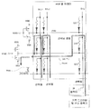
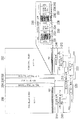
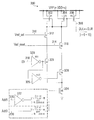
도 5는 동일한 로컬 그라운드 라인과 PMOS 및 NMOS(인버터)로 구성되는 서브-워드라인 드라이버를 통해 로우 상태가 되는 선택된 서브-워드라인 상의 피크 전류 집중을 줄일 수 있는 교번 서브-블록 유닛 선택을 구비한, 분할된 I/O 할당을 갖는 상변화 메모리 셀 어레이의 블록도이다.Figure 5 has alternating sub-block unit selections that can reduce peak current concentration on selected sub-word lines going low through a sub-wordline driver consisting of the same local ground line and PMOS and NMOS (inverter). Is a block diagram of a phase change memory cell array with divided I / O allocations.
도 5는 액세스될 제 1 PCM 메모리 어레이(200)와 제 2 PCM 어레이(202)를 도시한다. I/O 할당은, 제 1 PCM 메모리 어레이(200)는 IO(0~7)와 관련되고 제 2 PCM 메모리 어레이(202)는 IO(8~15)와 관련된다는 의미에서 분할된다. PCM 메모리 어레이(200)는 관련된 기록 드라이버 및 판독 센스 증폭기(210)와 열 선택 블록(214)을 가진다. 유사하게, PCM 메모리 어레이(202)는 관련된 기록 드라이버 및 판독 센스 증폭기(212)와 열 선택 블록(216)을 가진다. 어드레스 디코더(208)는 PCM 메모리 어레이(200)를 위한 메인 워드 라인 드라이버(204)에 연결되고 PCM 메모리 어레이(202)를 위한 메인 워드 라인 드라이버(206)에 연결된다. 판독/기록 제어 블록(218)은 판독 또는 기록의 수행이 이루어지고 있는지를 제어한다. 어드레스 레지스터(220)는 어떤 판독 또는 기록이 수행되는 지에 대한 어드레스를 포함한다. 열 어드레스 디코더(222)는 어드레스 레지스터의 출력을 수신하고 열 선택 블록(214, 216)으로 통과되는 출력(CA1~4)을 생성한다. 게다가, 어드레스 레지스터(220)의 출력(Add0)은 기록 드라이버 및 판독 센스 증폭기(210, 212)에 연결된다.5 shows a first
소자들(210, 212, 220)은 제 1 블록 세트와 제 2 블록 세트 사이에서 공동으로 선택한다. 더욱 일반적으로, 일부 실시예는 제 1 블록 세트와 제 2 블록 세트 사이에서 선택하도록 구성된 셀렉터를 갖는다. 소자들(210, 212, 220)은 이러한 셀렉터의 특정 예시를 구성하지만, 다른 구현도 가능하다.The
PCM 메모리 어레이(202)의 메인 워드라인의 반의 확대도는 일반적으로 230으로 표시된다. 메인 워드라인의 나머지 반은 PCM 어레이(200)에 위치한다. 다른 워드라인은 유사하다. 서브-워드라인 드라이버(231, 233, 235, 237, 240)의 부분들 사이에 위치되는 4개의 PCM 블록 유닛(232, 234, 236, 238)이 도시된다.An enlarged half of the main wordline of the
메인 워드라인이 2개로 분할되는 것을 바로 알 수 있다. 주어진 메인 워드라인의 반은 PCM 메모리 어레이(200)에 위치하고, 메인 워드라인의 나머지 반은 PCM 메모리 어레이(202)에 위치한다. 주어진 어드레스에 대하여, 교번 PCM 블록 유닛이 선택된다. 도시된 예시에서, PCM 블록 유닛(232, 236)은 음영 처리되어 선택을 표시한다. PCM 메모리 어레이(200)의 2개의 유닛 또한 선택되어(미도시), 총 4개의 PCM 메모리 어레이(200)가 선택된다. 각 PCM 블록 유닛이 4개의 비트를 저장하기 위하여 사용될 수 있다고 가정할 때, 16비트 워드가 선택된 PCM 블록 유닛에 기록될 수 있다.You can see immediately that the main wordline is split into two. One half of a given main wordline is located in
교번 PCM(상변화 메모리) 블록 유닛을 선택하기 위하여, 입력 어드레스, Add0가 도 5에서 도시된 바에 따라 선택 신호로서 사용된다. Add0는, 예컨대, 어드레스 비트의 LSB 또는 MSB가 될 수 있으며; 특정 선택은 PCM 설계의 어드레스 할당에 따른다. 도시된 예시에서, Add0가 0이면, 제 1 및 제 3 PCM 블록 유닛이 선택된다. 그 밖의 경우에, 제 2 및 제 4 PCM 블록 유닛이 선택된다(Add0=1인 경우).In order to select an alternating PCM (phase change memory) block unit, an input address, Add0, is used as the selection signal as shown in FIG. Add0 can be, for example, an LSB or MSB of address bits; The specific choice depends on the address assignment of the PCM design. In the example shown, if Add0 is zero, the first and third PCM block units are selected. In other cases, the second and fourth PCM block units are selected (if Add0 = 1).
이러한 분할된 IO 구성 및 교번 서브-블록 유닛 선택을 사용함으로써, 동시 프로그래밍이 수행되면, 그렇지 않았을 경우에 서브-워드라인 전압의 바람직하지 않은 상승을 유발할 수 있었던 그라운드 바운싱이 칩 면적 불이익(chip area penalty) 없이 효과적으로 억제될 수 있다. 또한, 어드레스 디코더의 중앙 배치로, 메인 워드라인과 서브-워드라인의 기생 저항 효과 또한 감소된다.By using this partitioned IO configuration and alternating sub-block unit selection, if the concurrent programming is performed, ground bouncing could result in an undesired rise in the sub-wordline voltage, resulting in a chip area penalty. Can be effectively suppressed without In addition, with the central arrangement of the address decoder, the parasitic resistance effect of the main word line and the sub-word line is also reduced.
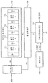
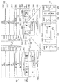
도 6은 도 5의 회로의 예시 구현을 도시한다. 적절한 곳에서, 유사 소자를 식별하기 위한 유사 참조 번호가 사용된다. 도 6의 예시에서, PCM 메모리 어레이(202)는 4개의 서브블록 어레이(250, 252, 254, 256)로 구성된다. 서브블록 어레이(256)의 상세가 도 6에 도시되나, 다른 서브 블록 어레이(250, 252, 524)는 이와 유사하다. 서브블록 어레이(256)는 n개의 메모리 셀 어레이 - 개별 메인 워드라인에 의해 각각 구동되고 이것들 중 3개의 메모리 셀 어레이(260, 262, 264)만 본 예시에 도시됨 - 로 구성된다. 메모리 셀 어레이(260)는 메인 워드라인(MWL0; 261)으로 구동되고; 메모리 셀 어레이(262)는 메인 워드라인(MWL1; 263)으로 구동되며, 메모리 셀 어레이(264)는 메인 워드라인(MWLn; 265)으로 구동된다. 메모리 셀 어레이(260)의 상세는 예시로서 도시되지만 다른 메모리 셀 어레이(262, 264)는 이와 유사하다. 메모리 셀 어레이(260)의 구조는 도 5와 관련되어 기재된 메모리 셀 어레이(참조 번호(230))와 유사하며, 5개의 서브-워드라인 구동기(231, 233, 235, 237, 240) 및 4개의 PCM 블록 유닛(232, 234, 236, 238)을 특징으로 한다. PCM 블록 유닛(232)과 같은 각각의 PCM 블록 유닛은 m개의 상변화 메모리 셀을 포함한다. 메모리 셀 어레이에 대한 메인 워드라인, 이런 경우에, MWL0은 서브-워드 드라이버(231, 233, 235, 237, 240)의 각각에 공통적으로 연결된다. 열 선택 회로(266)는 각 PCM 블록 유닛에 m개의 비트라인(BL)을 출력한다. 또한, 열 선택 회로(266)에 대한 m개의 DL(데이터 라인) 출력을 갖는 기록 드라이버/판독 센스 증폭기(212)가 도시된다.6 illustrates an example implementation of the circuit of FIG. 5. Where appropriate, like reference numerals are used to identify like elements. In the example of FIG. 6, the
PCM 메모리 어레이(200)에 대한 동일한 기능이 도시된다. PCM 메모리 어레이(202)의 메모리 셀 어레이(260) 및 PCM 메모리 어레이(200)의 메모리 셀 어레이(272)의 선택된 셀들은 하나의 16비트 저장 위치를 함께 형성한다.The same functionality for the
서브블록 어레이(260)의 확대된 회로도가 일반적으로 270으로 표시된다. 메인 워드라인(MWL0)은 각각의 서브-워드라인 드라이버(231, 233, 235, 237, 240)에 연결됨을 알 수 있다. 서브-워드라인 드라이버는 도 6에 도시된 바에 따라 동일한 서브 블록 어레이 내에서 공유되는 서브워드라인(SWL0; 242)을 구동한다. 일부 실시예에서, 서브-워드라인은 활성층 물질(n+)보다 금속 층 물질로 구현되고; 이런 종류의 연결은 서브-워드라인 기생 저항 효과를 줄이는 것을 돕는다.An enlarged circuit diagram of
도시된 실시예에서, 긴 메인 워드라인 길이로 인한 동작 지연을 줄이기 위하여, 어드레스 디코더가 칩의 중앙에 배치된다. 그러나, 일부 실시예에서, 교번 PCM 블록 유닛 선택을 특징으로 하는 도 6의 구조와 유사한 구조 - 오직 어드레스 디코더의 한쪽 사이드 상에 서브 블록 어레이의 단일 세트를 가짐 - 가 구현될 수 있으나, 이 경우 I/O 분할이 존재하지 않는다는 점이 이해되어야 한다.In the illustrated embodiment, in order to reduce the operation delay due to the long main word line length, an address decoder is placed in the center of the chip. However, in some embodiments, a structure similar to the structure of FIG. 6 featuring alternating PCM block unit selection, with only a single set of sub-block arrays on one side of the address decoder, can be implemented, in which case I It should be understood that there is no / O partition.
도 7은 Add0의 값의 함수로서 PCM 블록 유닛 선택의 특정 예시를 도시한다. 도 7의 상부(일반적으로 280으로 표시)는 Add0가 0인 경우에 대하여 메모리 셀 어레이(260)와 메모리 셀 어레이(270) 내의 PCM 블록 유닛 선택을 도시한다. 도면의 하부(일반적으로 282으로 표시)는 Add0가 1인 경우에 대하여 동일한 메모리 셀 어레이들에 대한 PCM 블록 유닛의 선택을 도시한다.7 shows a specific example of PCM block unit selection as a function of the value of Add0. The upper portion of FIG. 7 (generally indicated as 280) shows the PCM block unit selection in
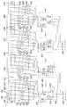
도 8a는 a) 분할 I/O 할당, b) 교번 서브블록 선택 및 c) 인접 셀 - 인접 셀로부터의 열 간섭을 피하도록 프로그래밍되지 않음 - 을 갖는 교번 비트라인 선택을 특징으로 하는 PCM 구성의 상세 예시이다.8A details a PCM configuration featuring a) split I / O allocation, b) alternating subblock selection, and c) alternating bitline selection with neighboring cells not programmed to avoid thermal interference from neighboring cells. It is an example.
메모리 셀 어레이에 대한 메인 워드라인은 400으로 표시되고 이것은 서브-워드라인 드라이버(402, 404, 406, 408, 410)에 연결된다. 메인 워드라인 및 서브워드라인 구조는 각 메모리 셀 어레이(셀들의 행)에 대해 반복된다. 메모리 셀 어레이는 4개의 PCM 블록 유닛(403, 405, 407, 409)을 포함한다. 제 1 PCM 블록 유닛(403)은 서브-워드라인 드라이버(402, 404) 사이에 있다. 비트라인 선택 트랜지스터 그룹(412, 414, 416, 418)은 활성화된 메인 워드라인의 제 1 PCM 블록 유닛 내에서 특정 셀을 선택하기 위해 사용된다. 비트라인 선택 트랜지스터 그룹(412)은 BL0, BL2, BL4 및 BL6을 인에이블링한다. 비트라인 선택 트랜지스터 그룹(414)은 BL1, BL3, BL5 및 BL7을 인에이블링한다. 유사하게 다른 그룹들도 비트라인의 개별 세트를 인에이블링한다. 실제로, 비트라인 선택 트랜지스터 그룹은 PCM 블록 유닛(403)의 셀들이 셀의 논리적인 그룹핑인 해당 셀 그룹으로 배열되도록 유도한다. 셀들의 각 논리적 그룹핑은 비트라인 선택 트랜지스터 그룹(412, 414, 416, 418)들 중 하나에 연결되는 PCM 셀들을 포함한다. 비트라인 선택 트랜지스터 그룹(412)에 해당하는 셀 그룹은 1번째, 3번째, 5번째 및 7번째 PCM 셀(490으로 공통적으로 표시됨)을 포함하고; 비트라인 선택 트랜지스터 그룹(414)에 해당하는 셀 그룹은 2번째, 4번째, 6번째 및 8번째 PCM 셀(492으로 공통적으로 표시됨)을 포함하며; 비트라인 선택 트랜지스터 그룹(416)에 해당하는 셀 그룹은 9번째, 11번째, 13번째 및 15번째 PCM 셀을 포함하고; 비트라인 선택 트랜지스터 그룹(418)에 해당하는 셀 그룹은 10번째, 12번째, 14번째 및 16번째 PCM 셀을 포함한다. 다른 PCM 블록 유닛(405, 407, 409)에 대한 PCM 셀이 유사하게 한정되어, 서브-워드라인 드라이버(404, 406) 사이의 PCM 블록 유닛(405)은 비트라인 선택 트랜지스터 그룹(420, 422, 424, 426)과 연관된 셀 그룹을 포함하고; 서브-워드라인 드라이버(406, 408) 사이의 PCM 블록 유닛(407)은 비트라인 선택 트랜지스터 그룹(428, 430, 432, 434)과 연관된 셀 그룹을 포함하며; 서브-워드라인 드라이버(408, 410) 사이의 PCM 블록 유닛(409)은 비트라인 선택 트랜지스터 그룹(436, 438, 440, 442)과 연관된 셀 그룹을 포함한다. 각 셀 그룹은 인접 셀을 포함하지 않고 셀 그룹의 부분을 형성하지 않는 하나의 중간 PCM 셀에 의해 이격된 4개의 PCM 셀들의 세트를 포함한다. 비트라인 선택 트랜지스터 그룹(412, 420, 428, 436)의 트랜지스터는 제 1 열 어드레스 신호(CA1; 450)에 공통적으로 연결된다. 비트라인 선택 트랜지스터 그룹(414, 422, 430, 438)의 트랜지스터는 제 2 열 어스레스 신호(CA2; 452)에 공통적으로 연결된다. 비트라인 선택 트랜지스터 그룹(416, 424, 432, 440)의 트랜지스터는 제 3 열 어스레스 신호(CA3; 454)에 공통적으로 연결된다. 비트라인 선택 트랜지스터 그룹(418, 426, 434, 442)의 트랜지스터는 제 4 열 어스레스 신호(CA4; 456)에 공통적으로 연결된다.The main wordline for the memory cell array is labeled 400 and it is connected to the
열 어드레스 디코더(222)는 열 어드레스 신호(CA1~CA4)를 생성한다. 더욱 일반적으로, 일부 실시예는 셀들의 제 1 세트와 셀들의 제 2 세트 사이에서 선택하기 위한 셀렉터를 갖는다. 열 어드레스 디코더(222)는 이러한 셀렉터의 특정 예시이다. 이러한 셀렉터의 관점에서, 이 셀렉터는 셀들의 제 1 세트에 연결된 제 1 출력을 가지며 셀들의 제 2 세트에 연결된 제 2 출력을 갖는다. 일부 실시예에서, 이러한 셀렉터는 셀들의 4개의 세트 사이에서 선택하기 위한 4개의 출력을 갖는다.The
PCM 블록 유닛(403)을 위한 기록 드라이버(460)의 세트가 도시된다. 기록 드라이버 0(462)은 4개의 비트라인 선택 트랜지스터 그룹(412, 414, 416, 418) 각각의 제 1 트랜지스터에 DL0L을 출력한다. 기록 드라이버 1(464)은 4개의 비트라인 선택 트랜지스터 그룹(412, 414, 416, 418) 각각의 제 2 트랜지스터에 DL1L을 출력한다. 기록 드라이버 2(466)는 4개의 비트라인 선택 트랜지스터 그룹(412, 414, 416, 418) 각각의 제 3 트랜지스터에 DL2L을 출력하고, 마지막으로, 기록 드라이버 3(468)은 4개의 비트라인 선택 트랜지스터 그룹(412, 414, 416, 418) 각각의 제 4 트랜지스터에 DL3L을 출력한다. CA1이 활성이면, DL0L, DL1L, DL2L 및 DL3L은 비트라인 선택 트랜지스터 그룹(412)과 관련된 셀 그룹에 전파된다. CA2이 활성이면, DL0L, DL1L, DL2L 및 DL3L은 비트라인 선택 트랜지스터 그룹(414)과 관련된 셀 그룹에 전파된다. CA3이 활성이면, DL0L, DL1L, DL2L 및 DL3L은 비트라인 선택 트랜지스터 그룹(416)과 관련된 셀 그룹에 전파된다. CA4가 활성이면, DL0L, DL1L, DL2L 및 DL3L은 비트라인 선택 트랜지스터 그룹(418)과 관련된 셀 그룹에 전파된다.A set of
기재된 실시예에서, 트랜지스터 그룹(412, 414)은 셀 그룹(490) 및 셀 그룹(492) 사이에서 선택하기 위해 사용된다. 더욱 일반적으로, 일부 실시예들은 비트라인의 제 1 세트(예컨대, BL0, BL2, BL4, BL6) 및 비트라인의 제 2 세트(예컨대, BL1, BL3, BL5, BL7)를 특징으로 하고, 각 비트라인은 비트라인을 선택하기 위한 스위칭 소자를 갖는다. 트랜지스터 그룹(412, 414)은 이러한 스위칭 소자의 특정 예시지만, 당업자는 다른 구현이 가능하다는 점을 이해할 것이다.In the described embodiment,
기록 드라이버(480, 482, 484)의 유사 세트가 각각의 제 2, 제 3 및 제 4 PCM 블록 유닛(405, 407, 409)의 대해 각각 도시된다. IO(IO0, IO1, IO2, IO3; 공통적으로 486으로 표시됨)는 기록 드라이버(460)에 연결되고, 또한 기록 드라이버(480)에 연결된다. 그러나, Add0이 0이면, 기록 드라이버(460)가 활성이고, 반면에, Add0이 1이면, 기록 드라이버(480)가 활성이다. 유사하게, IO(IO4, IO5, IO6, IO7; 공통적으로 488로 표시됨)는 기록 드라이버(482)와 기록 드라이버(484)에 입력된다. 그러나, Add0이 0이면, 기록 드라이버(482)가 활성이고, 반면에, Add0이 1이면, 기록 드라이버(484)가 활성이다.Similar sets of
유사 구조는 판독 센싱에 대해 제공되지만 상세는 도면에 포함되지 않는다.Similar structures are provided for read sensing but details are not included in the figures.
일부 실시예에서, 각 기록 드라이버는, Add0이 0인 경우에 대한 하나, 'L'접미사, 및 Add0이 1인 경우에 대한 PCM 블록 유닛, 'R'접미사를 포함시키는, 2개의 PCM 블록 유닛들 간의 짧은 데이터 라인 연결을 갖기 위해 배치된다. 예컨대, 기록 드라이버와 DL 라인 사이에서 스위치를 하나 더 사용하여, 403과 405 모두에 대해 공통 기록 드라이버가 사용될 수 있다. 그러므로, Add0은 기록 드라이버 인에이블 대신 스위치 선택에 사용된다. 선택되지 않은 기록 드라이버는 셀에 전류를 구동하지 않는다. CA1~4 신호(450, 452, 454, 456)는 어드레스 입력 디코딩 결합에 따라 비트라인을 선택하기 위해 사용된다. 4개의 CA1~4 신호 중 하나만이 하이 상태가 되고, 하이 CA 신호에 연결되는 NMOS 트랜지스터는 턴온된다.In some embodiments, each write driver includes two PCM block units, including one for the case where Add0 is 0, a 'L' suffix, and a PCM block unit for the case where Add0 is 1, and an 'R' suffix. It is arranged to have a short data line connection between them. For example, using one more switch between the write driver and the DL line, a common write driver can be used for both 403 and 405. Therefore, Add0 is used for switch selection instead of write driver enable. Unselected write drivers do not drive current in the cell. The CA1-4
요약하자면, (그 중 하나가 도 8a의 워드라인(400)인) 워드라인, CA1, CA2, CA3, CA4 신호 및 Add0 입력은 어느 셀이 활성인지를 제어하기 위해 함께 동작한다.In summary, the wordline, CA1, CA2, CA3, CA4 signal and one of the Add0 inputs (one of which is the
워드라인 : 특정 메인 워드라인(예컨대, 메인 워드라인(400))의 활성화는 메모리 어레이의 특정 행을 선택한다. 일부 실시예에서, 워드라인은 워드라인 상의 로우 상태에 의해 활성화된다. 모든 서브 워드라인은 공통적으로 메인 워드라인에 연결되므로, 주어진 워드라인의 선택은 이 워드라인에 연결되는 모든 서브 워드라인을 그에 따라 선택한다. 선택된 서브-워드라인은 서브-워드라인 드라이버를 통해 그라운드 레벨에 설정되어서 선택된 다이오드 스위치를 턴온한다. 선택해제된 서브-워드라인은 동작 모드에 따라 VDD+1V 또는 VDD+2V(α = 1V 또는 2V) 레벨에 설정되어 선택해제된 다이오드 스위치를 턴오프한다. Wordline : Activation of a particular main wordline (eg, main wordline 400) selects a particular row of the memory array. In some embodiments, the wordline is activated by the low state on the wordline. Since all sub word lines are commonly connected to the main word line, the selection of a given word line selects all sub word lines connected to this word line accordingly. The selected sub-wordline is set at ground level via the sub-wordline driver to turn on the selected diode switch. The deselected sub-wordline is set at the level of VDD + 1V or VDD + 2V (α = 1V or 2V) to turn off the deselected diode switch.
CA1 , CA2 , CA3 , CA4: 이 신호들은 위에서 상세히 기재된 바에 따르면 PCM 블록 유닛 내에서 상이한 해당 서브셋들 사이에서 셀을 선택한다. 선택해제된 비트라인(B/L)은 플로팅(전압 또는 전류 구동 상태 없음)에 설정되어서 일반적인 기록 동작에서의 누설전류 및 기생 효과를 감소시킨다. CA1 , CA2 , CA3 , CA4 : These signals select a cell between different corresponding subsets within the PCM block unit as detailed above. The deselected bit lines B / L are set to floating (no voltage or current driving states) to reduce leakage current and parasitic effects in normal write operations.
Add0 - 이 입력은 어떤 기록 드라이버의 세트가 활성인지 제어한다. 기록 드라이버에서의 기록 전류(Iwrite)는 데이터 형태에 따라 선택된 비트라인(B/L)으로 흐른다(IO 값 = 0 → 세트 전류 구동, IO 값 = 1 → 리세트 전류 구동). 기록 드라이버 전류는 서브-워드라인 로우 상태에 의해 선택된 셀로 구동된다.Add0-This input controls which write driver set is active. The write current Iwrite in the write driver flows to the selected bit line B / L according to the data type (IO value = 0 → set current drive, IO value = 1 → reset current drive). The write driver current is driven to the cell selected by the sub-wordline low state.
이하의 표는 입력 퍼뮤테이션(permutation) 및 결과적으로 선택된 셀을 기재한다: The following table lists the input permutation and consequently the selected cells:
입력의 퍼뮤테이션 각각에 있어서, 8개의 선택된 메모리 셀이 존재함을 알 수 있다. 동일 구조가 반복될 경우, 도 6의 예시에서와 같이, 어드레스 디코더의 다른 사이드 상에서, 입력의 퍼뮤테이션 각각은 총 16개의 메모리 셀을 선택한다.It can be seen that for each permutation of the input, there are eight selected memory cells. If the same structure is repeated, as in the example of Figure 6, on the other side of the address decoder, each of the permutations of the input selects a total of 16 memory cells.
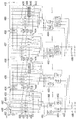
예시로서, 도 8b는 CA1이 선택되고 Add0이 0인 경우에 대하여 음영처리된 선택된 셀을 도시한다. 도 8c는 CA3이 선택되고 Add0이 1인 경우에 대하여 음영처리된 선택된 셀을 도시한다.As an example, FIG. 8B shows selected cells shaded for the case where CA1 is selected and Add0 is zero. 8C shows the selected cells shaded for the case where CA3 is selected and Add0 is one.
도 9는 어드레스 제어를 갖는 기록 드라이버의 상세 예시이다. 데이터 비트는 IOi(318)에서 입력된다. 이것은 인버터(INV1; 320)에서 반전되고, 이것의 출력은 트랜지스터(N3; 321)의 게이트에 연결된다. INV1(320)의 출력은 또한 인버터(INV2; 326)에 입력되며, 이것의 출력은 트랜지스터(N4; 328)의 게이트에 연결된다. 기준 전압(Vref_set)은 310에서 트랜지스터(N1; 312)의 게이트에 입력된다. 리세트 동작에 대한 기준 전압이 입력되고, Vref_reset(314)는 트랜지스터(N2, 316)의 게이트에 입력된다. 트랜지스터 P1(302), P2(304) 및 P3(306)을 포함하는 전류 미러 구조(300)가 도시된다. P1(302) 및 P2(304)의 모든 단자는 공통적으로 연결되고 단일 PMOS 트랜지스터에 대안적으로 병합될 수 있다는 점이 주목된다. 트랜지스터 (P1; 302) 및 (P2; 304)의 게이트는 출력 전류(308)를 생성하는 트랜지스터 (P3; 306)의 게이트에 연결된다. 홀수 블록에 있어서, 출력은 DLiL인 반면, 짝수 블록에 있어서, 출력은 DLiR이며, 여기서 i가 0 내지 15이다. 홀수 블록 또는 짝수 블록의 선택 여부는 어드레스 입력(330)에 의해 제어된다. 홀수 블록을 위한 기록 드라이버에서, 어드레스 입력(Add0; 330)은 인버터(332)를 통해 트랜지스터(N5; 334)의 게이트에 연결된다. 반대로, 짝수 블록 유닛에서, 어드레스 입력(Add0; 330)은 트랜지스터(N5; 334)의 게이트에 바로 연결된다. 선택해제될 비트라인에 연결된 주어진 기록 드라이버에 있어서, Add0(330)은 (도시된 실시예에서, 홀수 블록 유닛에 대해 하이 상태가 되거나, 짝수 블록 유닛에 대해 로우 상태가 되어서) 연결된 NMOS N5(334)를 턴오프한다. 결과적으로, P1(302), P2(304) 및 P3(306)의 오프 상태로 인한 전류 구동은 존재하지 않으며, DLiL/DLiR은 플로팅 상태를 갖게 된다(전류 구동 상태 없음). 선택될 비트라인에 연결된 주어진 기록 드라이버에 있어서, Add0(330)은 연결된 NMOS N5(334)를 턴온시킨다. 일단 P1(302) 및 P2(304)가 세트 또는 리세트으로 인해 턴온하면, 기록 드라이버는 P3(306)를 통해 DLiL 또는 DLiR(308)로 전류를 소환한다(invoke). 전류량은 어떤 데이터가 어서트(assert)되는지에 따라 결정된다. 인버터(INV1; 320, INV2; 326) 및 트랜지스터(N3; 321, N4, 328)의 논리를 통해, IOi가 하이 상태(논리 '1')이면, 비정질 전류는 P3(306)에서 DLiL 또는 DLiR(308)로 소환되고, 반면에, IOi가 로우 상태(논리 '0')이면, 결정 전류는 P3(306)에서 DLiL 또는 DLiR(308)로 소환된다.9 is a detailed example of a write driver with address control. The data bits are input at
구체적으로, IOi(318)가 로우 상태(논리 '0')이면, NMOS(N3; 321)가 턴온되고 Vref_set가 연결된 NMOS(N1; 312)가 N3(321)의 온 상태에 의해 턴온된다. 이것으로, P1(302) 및 P2(304)의 드레인 및 게이트가 로우 상태가 되고, 전류 미러 구조로 인하여, P1 및 P2에서 나오는 전류의 합과 같은 전류는 P3(306)에 소환되어 DLiL 또는 DLiR(308)을 생성한다. IOi의 하이 상태(논리 '1')의 경우, NMOS (N4; 328)은 턴온되고, NMOS (N2; 316)에 연결된 Vref_reset은 N4(328)의 상태에 의해 턴온된다. 이런 경우에, 다시, P1(302) 및 P2(304)의 드레인 및 게이트가 로우 상태 상태가 되고, 전류 미러 구조로 인하여, P1 및 P2에서 나오는 전류의 합과 같은 전류는 PMOS P3 PMOS 트랜지스터(306)에 소환되어 DLiL 또는 DLiR(308)을 생성한다. 트랜지스터 N3(321) 및 N4(328)가 상이한 크기를 가져서 논리 '1' 경우에 대해 소환된 전류는 논리 '0' 경우와 상이하다. 특정 예시에서, 세트 전류는 약 0.2mA인 반면에, 리세트 전류는 약 1mA이지만, 상이한 값이 셀 구현에 따라 사용될 수 있다는 점이 확실히 이해되어야 한다. Add0 신호를 사용하여, 홀수 블록 또는 짝수 블록이 선택될 수 있다. 상이한 펄스 지속 기간은 IOi의 하이 상태가 아닌 로우 상태를 위해 생성된다. 이것은 Vref_set 및 Vref_reset의 펄스 폭을 제어하여 제어될 수 있어서 Vref_reset에 대한 펄스 폭이 Vref_set에 대한 것보다 길다. 대안적으로, 상이한 펄스 폭은 논리 '0'이 아닌 논리 '1'을 위한 IOi를 위해 사용될 수 있다.Specifically, when
도 10은 셀에 기록하기 위한 신호의 타이밍을 도시하는 상세 타이밍 도이다.10 is a detailed timing diagram showing timing of signals for writing to a cell.
상기 기재된 실시예는 a) 분할된 IO, b) 교번 서브-블록 선택, 및 c) 교번 비트-라인의 3가지 특성을 포함한다. 더욱 일반적으로, 일부 실시예에서, 이러한 특성 중 하나 또는 두 가지를 포함하는 PCM 구성이 제공된다.The embodiment described above includes three characteristics: a) partitioned IO, b) alternating sub-block selection, and c) alternating bit-line. More generally, in some embodiments, a PCM configuration is provided that includes one or both of these features.
상기 기재된 실시예에서, 장치 소자 및 회로는 간결성을 위해 도면에서 도시된 대로 서로 연결된다. 본 발명의 실제 응용에서, 소자, 회로 등은 서로 직접적으로 연결될 수 있다. 또한, 소자, 회로 등은 장치 및 기구의 동작에 필요한 다른 소자, 회로 등을 통해 서로에게 간접적으로 연결될 수 있다. 그러므로, 실제 구성에서, 회로 소자 및 회로는 직접적으로 또는 간접적으로 서로에게 결합 또는 연결된다.In the embodiment described above, the device elements and circuits are connected to each other as shown in the figures for the sake of brevity. In practical applications of the present invention, elements, circuits, etc. may be directly connected to each other. In addition, elements, circuits, and the like may be indirectly connected to each other through other elements, circuits, and the like, necessary for the operation of the device and the apparatus. Therefore, in a practical configuration, the circuit elements and the circuits are coupled or connected to each other directly or indirectly.
본 발명의 상기 기재된 실시예는 오직 예시적인 것이다. 오로지 본 명세서에 첨부된 청구항에 의해 한정되는 본 발명의 권리범위에서 벗어나지 않는, 당업자의 특정 실시예의 변경, 수정 및 변형은 가능하다.
The above described embodiments of the invention are illustrative only. Modifications, modifications and variations of the specific embodiments of those skilled in the art are possible without departing from the scope of the invention as defined solely by the claims appended hereto.
Claims (29)
액세스하기 위한 메모리 위치가 상기 PCM 셀들의 서브셋을 포함하여, 상기 서브셋의 PCM 셀 각각은 상기 서브셋의 다른 PCM 셀과 서로 인접하지 않는, 장치.A plurality of adjacent Phase Change Memory (PCM) cells;
Wherein the memory location for access comprises a subset of the PCM cells, wherein each of the PCM cells in the subset is not adjacent to each other with other PCM cells in the subset.
상기 복수의 인접한 PCM 셀은 홀수 PCM 셀들의 제 1 세트와 짝수 PCM 셀들의 제 2 세트로 나뉘어져서, 상기 제 1 세트와 제 2 세트의 셀들은 상기 제 1 세트에 속한 것과 상기 제 2 세트에 속한 것 사이에서 교번하며;
상기 장치는 상기 셀들의 제 1 세트 또는 상기 셀들의 제 2 세트를 선택하기 위한 셀렉터를 더 포함하는, 장치.The method according to claim 1,
The plurality of adjacent PCM cells is divided into a first set of odd PCM cells and a second set of even PCM cells, such that the first and second sets of cells belong to the first set and belong to the second set. Alternating between;
And the apparatus further comprises a selector for selecting the first set of cells or the second set of cells.
상기 셀렉터가 상기 셀들의 제 1 세트를 선택하면, 판독 또는 기록을 위한 메모리 위치는 상기 셀들의 제 1 세트를 포함하고 상기 셀들의 제 2 세트는 포함하지 않으며,
상기 셀렉터가 상기 셀들의 제 2 세트를 선택하면, 판독 또는 기록을 위한 메모리 위치는 상기 셀들의 제 2 세트를 포함하고 상기 셀들의 제 1 세트는 포함하지 않는, 장치.The method according to claim 2,
If the selector selects the first set of cells, the memory location for read or write includes the first set of cells and does not include the second set of cells,
If the selector selects the second set of cells, the memory location for read or write includes the second set of cells and does not include the first set of cells.
상기 셀들의 제 1 세트에 연결된 제 1 출력;
상기 셀들의 제 2 세트에 연결된 제 2 출력을 포함하는, 장치. The method according to claim 2, wherein the selector,
A first output coupled to the first set of cells;
And a second output coupled to the second set of cells.
상기 복수의 인접한 PCM 셀은 홀수 PCM 셀의 제 3 세트와 짝수 PCM 셀의 제 4 세트를 더 포함하며, 상기 제 3 세트와 제 4 세트의 셀들은 상기 제 3 세트에 속한 것과 상기 제 4 세트에 속한 것 사이에서 교번하며;
상기 셀렉터는,
상기 셀들의 제 1 세트에 연결된 제 1 출력;
상기 셀들의 제 2 세트에 연결된 제 2 출력;
상기 셀들의 제 3 세트에 연결된 제 3 출력; 및
상기 셀들의 제 4 세트에 연결된 제 4 출력을 포함하는, 장치.The method according to claim 2,
The plurality of contiguous PCM cells further comprises a third set of odd PCM cells and a fourth set of even PCM cells, wherein the third and fourth sets of cells belong to the third set and to the fourth set. Alternating between belongings;
The selector
A first output coupled to the first set of cells;
A second output coupled to the second set of cells;
A third output coupled to the third set of cells; And
And a fourth output coupled to the fourth set of cells.
비트라인들의 제 1 세트 및 비트라인들의 제 2 세트를 더 포함하고, 각각의 비트라인은 상기 비트라인을 선택하기 위한 스위칭 소자를 포함하며;
상기 비트라인의 제 1 세트의 스위칭 소자들은 제 1 출력에 연결되고 상기 비트라인들의 제 2 세트의 스위칭 소자들은 제 2 출력에 연결되는, 장치.The method according to claim 2,
Further comprising a first set of bit lines and a second set of bit lines, each bit line including a switching element for selecting the bit line;
And the switching elements of the first set of bit lines are connected to a first output and the switching elements of the second set of bit lines are connected to a second output.
상기 제 1 블록 세트와 상기 제 2 블록 세트 사이에서 선택하도록 구성되는 제 1 셀렉터; 및
워드라인 드라이버 구조 - 제 1 복수의 서브-워드라인 드라이버; 및 상기 제 1 복수의 서브-워드라인 드라이버를 통해 상기 제 1 복수의 PCM 블록 유닛을 구동하는 제 1 메인 워드라인 드라이버를 포함함 - 를 포함하고,
상기 제 1 셀렉터가 상기 제 1 블록 세트를 선택하면, 액세스하기 위한 메모리 위치는 상기 제 1 블록 세트의 각 블록의 메모리 셀을 포함하고, 상기 제 1 셀렉터가 상기 제 2 블록 세트를 선택하면, 액세스하기 위한 메모리 위치는 상기 제 2 메모리 세트의 각 블록의 메모리 셀들을 포함하는, 장치.A first plurality of PCM block units, each PCM block unit comprising a plurality of memory cells, wherein the first plurality of PCM block units are divided into a first set of blocks and a second set of blocks, thereby providing a first set of blocks. Each PCM block unit belonging to is not adjacent to any other PCM block unit in the first block set, and each PCM block unit belonging to the second block set is not adjacent to any other PCM block unit in the second block set. A first memory cell array comprising;
A first selector configured to select between the first block set and the second block set; And
Wordline driver structure-a first plurality of sub-wordline drivers; And a first main wordline driver for driving the first plurality of PCM block units through the first plurality of sub-wordline drivers.
If the first selector selects the first block set, the memory location for access includes the memory cells of each block of the first block set, and if the first selector selects the second block set, access And a memory location to comprise memory cells of each block of the second memory set.
복수의 인접한 PCM(상변화 메모리) 셀을 포함하고;
상기 제 1 셀렉터에 의해 선택된 PCM 블록 유닛에 대하여, 액세스하기 위한 상기 메모리 위치는 상기 PCM 블록 유닛의 PCM 셀들의 서브셋을 포함하여, 상기 서브셋의 각 PCM 셀은 상기 서브셋의 다른 PCM셀과 서로 인접하지 않는, 장치.The method of claim 7, wherein each PCM block unit is:
A plurality of adjacent PCM (phase change memory) cells;
For the PCM block unit selected by the first selector, the memory location for access includes a subset of PCM cells of the PCM block unit, such that each PCM cell in the subset is not adjacent to each other in the subset. Do not, the device.
상기 장치는 상기 셀들의 제 1 세트와 상기 셀들의 제 2 세트 사이에서 선택하는 제 2 셀렉터를 더 포함하는, 장치.9. The method of claim 8, wherein each PCM block unit comprises a plurality of contiguous memory cells divided into a first set of odd memory cells and a second set of even memory cells, wherein the first and second sets of cells are the first set of cells. Alternating between belonging to the set and belonging to the second set;
And the apparatus further comprises a second selector to select between the first set of cells and the second set of cells.
상기 제 1 셀렉터가 상기 제 1 블록 세트를 선택하고 상기 제 2 셀렉터가 상기 셀들의 제 1 세트를 선택하면, 판독 또는 기록을 위한 메모리 위치는 상기 제 1 블록 세트의 각 블록의 셀들의 제 1 세트의 메모리 셀들을 포함하고;
상기 제 1 셀렉터가 상기 제 1 블록 세트를 선택하고 상기 제 2 셀렉터가 상기 셀들의 제 2 세트를 선택하면, 판독 또는 기록을 위한 메모리 위치는 상기 제 1 블록 세트의 각 블록의 셀들의 제 2 세트의 메모리 셀들을 포함하고;
상기 제 1 셀렉터가 상기 제 2 블록 세트를 선택하고 상기 제 2 셀렉터가 상기 셀들의 제 1 세트를 선택하면, 판독 또는 기록을 위한 메모리 위치는 상기 제 2 블록 세트의 각 블록의 셀들의 제 1 세트의 메모리 셀들을 포함하며;
상기 제 1 셀렉터가 상기 제 2 블록 세트를 선택하고 상기 제 2 셀렉터가 상기 셀들의 제 2 세트를 선택하면, 판독 또는 기록을 위한 메모리 위치는 상기 제 2 블록 세트의 각 블록의 셀들의 제 2 세트의 메모리 셀들을 포함하는, 장치.The method of claim 9,
If the first selector selects the first block set and the second selector selects the first set of cells, the memory location for reading or writing is the first set of cells of each block of the first block set. Memory cells of;
If the first selector selects the first block set and the second selector selects the second set of cells, the memory location for reading or writing is the second set of cells of each block of the first block set. Memory cells of;
If the first selector selects the second block set and the second selector selects the first set of cells, the memory location for reading or writing is the first set of cells of each block of the second block set. Memory cells of;
If the first selector selects the second block set and the second selector selects the second set of cells, the memory location for reading or writing is the second set of cells of each block of the second block set. And memory cells of the device.
각 PCM 블록에 대하여, 상기 복수의 인접한 PCM 셀은 홀수 PCM 셀들의 제 3 세트 및 짝수 PCM 셀들의 제 4 세트를 더 포함하여, 상기 제 3 및 제 4 세트의 셀들은 상기 제 3 세트에 속한 것과 상기 제 4 세트에 속한 것 사이에서 교번하고;
상기 제 2 셀렉터는,
상기 셀들의 제 1 세트에 연결된 제 1 출력;
상기 셀들의 제 2 세트에 연결된 제 2 출력;
상기 셀들의 제 3 세트에 연결된 제 3 출력; 및
상기 셀들의 제 4 세트에 연결된 제 4 출력을 포함하는, 장치.The method of claim 9,
For each PCM block, the plurality of contiguous PCM cells further comprises a third set of odd PCM cells and a fourth set of even PCM cells, such that the third and fourth sets of cells belong to the third set. Alternating between those belonging to the fourth set;
The second selector is,
A first output coupled to the first set of cells;
A second output coupled to the second set of cells;
A third output coupled to the third set of cells; And
And a fourth output coupled to the fourth set of cells.
제 2 복수의 PCM 블록 유닛 - 상기 제 2 복수의 PCM 블록 유닛은 제 3 블록 세트와 제 4 블록 세트로 나뉘어져서, 상기 제 3 세트에 속한 각각의 PCM 블록 유닛은 상기 제 3 세트의 어떤 다른 PCM 블록 유닛에 인접하지 않으며, 상기 제 4 세트에 속하는 각각의 PCM 블록 유닛은 상기 제 4 세트의 어떤 다른 PCM 블록 유닛과 인접하지 않음 - 을 포함하는 제 2 메모리 셀 어레이를 더 포함하고;
상기 워드라인 드라이버 구조는 제 2 복수의 서브-워드라인 드라이버를 통해 상기 제 2 복수의 PCM 블록 유닛을 구동하는 제 2 메인 워드라인 드라이버를 더 포함하며;
상기 제 1 셀렉터는,
a) 상기 제 1 블록 세트와 상기 제 3 블록 세트의 양쪽;
b) 상기 제 2 블록 세트와 상기 제 4 블록 세트의 양쪽 중 하나를 선택하되;
상기 셀렉터가 상기 제 1 블록 세트와 상기 제 3 블록 세트를 선택하면, 액세스하기 위한 메모리 위치는 상기 제 1 블록 세트의 각 블록의 메모리 셀들과 상기 제 3 블록 세트의 각 블록의 메모리 셀들을 포함하고;
상기 셀렉터가 상기 제 2 블록 세트와 상기 제 4 블록 세트를 선택하면, 액세스하기 위한 메모리 위치는 상기 제 2 블록 세트의 각 블록의 메모리 셀들과 상기 제 4 블록 세트의 각 블록의 메모리 셀들을 포함하는, 장치.The device of claim 7 wherein the device is:
A second plurality of PCM block units, wherein the second plurality of PCM block units are divided into a third block set and a fourth block set such that each PCM block unit belonging to the third set is any other PCM of the third set; A second memory cell array further comprising a second memory cell array that is not adjacent to a block unit and each PCM block unit belonging to the fourth set is not adjacent to any other PCM block unit of the fourth set;
The wordline driver structure further comprises a second main wordline driver for driving the second plurality of PCM block units through a second plurality of sub-wordline drivers;
The first selector is,
a) both of the first block set and the third block set;
b) select one of both the second block set and the fourth block set;
If the selector selects the first block set and the third block set, the memory location for access includes memory cells of each block of the first block set and memory cells of each block of the third block set; ;
If the selector selects the second block set and the fourth block set, the memory location for access includes memory cells of each block of the second block set and memory cells of each block of the fourth block set. , Device.
어드레스 디코더를 포함하고;
상기 제 1 메인 워드라인 드라이버 및 상기 제 2 메인 워드라인 드라이버가 상기 어드레스 디코더에 의해 공통적으로 활성화되는, 장치.The method of claim 12,
An address decoder;
And the first main wordline driver and the second main wordline driver are commonly activated by the address decoder.
각 PCM 블록 유닛은 복수의 인접한 PCM(상변화 메모리) 셀들을 포함하고;
상기 제 1 셀렉터에 의해 선택된 PCM 블록 유닛에 대하여, 상기 액세스하기 위한 메모리 위치는 상기 PCM 블록 유닛의 PCM 셀들의 서브셋을 포함하여, 상기 서브셋의 각 PCM 셀은 상기 서브셋의 다른 PCM 셀과 서로 인접하지 않는, 장치.The method of claim 12,
Each PCM block unit comprises a plurality of adjacent PCM (phase change memory) cells;
For the PCM block unit selected by the first selector, the memory location for access includes a subset of PCM cells of the PCM block unit such that each PCM cell of the subset is not adjacent to each other other PCM cells in the subset. Do not, the device.
각 PCM 블록 유닛은, 홀수 메모리 셀들의 제 1 세트 및 짝수 메모리 셀들의 제 2 세트로 나뉘는 복수의 인접한 메모리 셀을 포함하여, 상기 제 1 및 제 2 세트의 셀들은 상기 제 1 세트에 속한 것과 상기 제 2 세트에 속한 것 사이에서 교번하고;
상기 장치는 상기 셀들의 제 1 세트와 셀들의 제 2 세트 사이에서 선택하는 제 2 셀렉터를 더 포함하는, 장치.The method according to claim 14,
Each PCM block unit includes a plurality of contiguous memory cells divided into a first set of odd memory cells and a second set of even memory cells, such that the first and second sets of cells belong to the first set and the Alternate between belonging to the second set;
And the apparatus further comprises a second selector to select between the first set of cells and the second set of cells.
상기 제 1 셀렉터가 상기 제 1 블록 세트를 선택하고 상기 제 2 셀렉터가 상기 셀들의 제 1 세트를 선택하면, 판독 또는 기록을 위한 메모리 위치는 상기 제 1 블록 세트의 각 블록의 셀들의 제 1 세트의 메모리 셀들을 포함하고;
상기 제 1 셀렉터가 상기 제 1 블록 세트를 선택하고 상기 제 2 셀렉터가 상기 셀들의 제 2 세트를 선택하면, 판독 또는 기록을 위한 메모리 위치는 상기 제 1 블록 세트의 각 블록의 셀들의 제 2 세트의 메모리 셀들을 포함하고;
상기 제 1 셀렉터가 상기 제 2 블록 세트를 선택하고 상기 제 2 셀렉터가 상기 셀들의 제 1 세트를 선택하면, 판독 또는 기록을 위한 메모리 위치는 상기 제 2 블록 세트의 각 블록의 셀들의 제 1 세트의 메모리 셀들을 포함하며;
상기 제 1 셀렉터가 상기 제 2 블록 세트를 선택하고 상기 제 2 셀렉터가 상기 셀들의 제 2 세트를 선택하면, 판독 또는 기록을 위한 메모리 위치는 상기 제 2 블록 세트의 각 블록의 셀들의 제 2 세트의 메모리 셀들을 포함하는, 장치.The method according to claim 14,
If the first selector selects the first block set and the second selector selects the first set of cells, the memory location for reading or writing is the first set of cells of each block of the first block set. Memory cells of;
If the first selector selects the first block set and the second selector selects the second set of cells, the memory location for reading or writing is the second set of cells of each block of the first block set. Memory cells of;
If the first selector selects the second block set and the second selector selects the first set of cells, the memory location for reading or writing is the first set of cells of each block of the second block set. Memory cells of;
If the first selector selects the second block set and the second selector selects the second set of cells, the memory location for reading or writing is the second set of cells of each block of the second block set. And memory cells of the device.
각 PCM 블록에 대하여, 상기 복수의 인접한 PCM 셀은 홀수 PCM 셀들의 제 3 세트 및 짝수 PCM 셀들의 제 4 세트를 더 포함하여, 상기 제 3 및 제 4 세트의 셀들은 상기 제 3 세트에 속한 것과 상기 제 4 세트에 속한 것 사이에서 교번하고;
상기 셀렉터는 상기 셀들의 제 1 세트를 선택하도록 연결된 제 1 출력, 상기 셀들의 제 2 세트를 선택하도록 연결된 제 2 출력, 상기 셀들의 제 3 세트를 선택하도록 연결된 제 3 출력, 및 상기 셀들의 제 4 세트를 선택하도록 연결된 제 4 출력을 포함하는, 장치.18. The method of claim 16,
For each PCM block, the plurality of contiguous PCM cells further comprises a third set of odd PCM cells and a fourth set of even PCM cells, such that the third and fourth sets of cells belong to the third set. Alternating between those belonging to the fourth set;
The selector comprises a first output coupled to select the first set of cells, a second output coupled to select the second set of cells, a third output coupled to select the third set of cells, and a first of the cells And a fourth output coupled to select four sets.
제 1 PCM 어레이 및 제 2 PCM 어레이를 포함하는 메모리 셀 어레이 - 상기 제 1 PCM 어레이는 제 1 복수의 PCM 블록 유닛을 포함하고, 상기 제 2 PCM 어레이는 제 2 복수의 PCM 블록 유닛을 포함함 -;
워드라인 드라이버 구조 - 복수의 워드라인 각각에 대하여, 상기 제 1 복수의 PCM 블록 유닛을 구동하도록 구성된 제 1 복수의 서브-워드 드라이버를 통해 상기 제 1 PCM 어레이를 구동하도록 구성되는 제 1 메인 워드라인 드라이버; 상기 제 2 복수의 PCM 블록 유닛을 구동하도록 구성된 제 2 복수의 서브-워드 드라이버를 통해 상기 제 2 PCM 어레이를 구동하도록 구성되는 제 2 메인 워드라인 드라이버 를 포함함 - ;
제 1 메인 워드라인 드라이버와 제 2 메인 워드라인 드라이버를 공통적으로 활성화하도록 구성된 어드레스 디코더를 포함하고,
액세스하기 위한 메모리 위치는 상기 제 1 메모리 셀 어레이의 선택된 메모리 셀들과 상기 제 2 메모리 셀 어레이의 선택된 메모리 셀들을 포함하는, 메모리 장치.A memory device comprising:
A memory cell array comprising a first PCM array and a second PCM array, wherein the first PCM array comprises a first plurality of PCM block units and the second PCM array includes a second plurality of PCM block units ;
Wordline driver structure-a first main wordline configured to drive the first PCM array through a first plurality of sub-word drivers configured to drive the first plurality of PCM block units for each of a plurality of wordlines driver; A second main wordline driver configured to drive the second PCM array via a second plurality of sub-word drivers configured to drive the second plurality of PCM block units;
An address decoder configured to commonly activate the first main wordline driver and the second main wordline driver,
And the memory location for accessing comprises selected memory cells of the first memory cell array and selected memory cells of the second memory cell array.
상기 복수의 인접한 PCM 셀이 홀수 PCM 셀들의 제 1 세트와 짝수 PCM 셀들의 제 2세트로 나뉘어져서, 상기 제 1 및 제 2 세트의 셀들은 상기 제 1 세트에 속한 것과 상기 제 2 세트에 속한 것 사이를 교번하고;
상기 방법은 상기 셀들의 제 1 세트 또는 상기 셀들의 제 2 세트를 선택하는 단계를 더 포함하는, 방법.The method of claim 20,
Wherein the plurality of adjacent PCM cells is divided into a first set of odd PCM cells and a second set of even PCM cells, such that the first and second sets of cells belong to the first set and belong to the second set Alternating between;
The method further comprises selecting the first set of cells or the second set of cells.
상기 셀렉터가 상기 셀들의 제 1 세트를 선택하면, 판독 또는 기록을 위한 메모리 위치는 상기 셀들의 제 1 세트를 포함하고 상기 셀들의 제 2 세트는 포함하지 않으며,
상기 셀렉터가 상기 셀들의 제 2 세트를 선택하면, 판독 또는 기록을 위한 메모리 위치는 상기 셀들의 제 2 세트를 포함하고 상기 셀들의 제 1 세트는 포함하지 않는, 방법.23. The method of claim 21,
If the selector selects the first set of cells, the memory location for read or write includes the first set of cells and does not include the second set of cells,
If the selector selects the second set of cells, the memory location for read or write includes the second set of cells and does not include the first set of cells.
상기 복수의 인접한 PCM 셀은 홀수 PCM 셀들의 제 3 세트와 짝수 PCM 셀들의 제 4 세트를 더 포함하여, 상기 제 3 및 제 4 세트의 셀들은 상기 제 3 세트에 속한 것과 상기 제 4 세트에 속한 것 사이를 교번하고;
상기 방법은 상기 셀들의 제 1 세트, 상기 셀들의 제 2 세트, 상기 셀들의 제 3 세트 및 상기 셀들의 제 4 세트 사이에서 선택하는 단계를 더 포함하는, 방법.23. The method of claim 21,
The plurality of contiguous PCM cells further includes a third set of odd PCM cells and a fourth set of even PCM cells, such that the third and fourth sets of cells belong to the third set and belong to the fourth set. Alternating between things;
The method further comprising selecting between the first set of cells, the second set of cells, the third set of cells and the fourth set of cells.
제 1 복수의 PCM 블록 유닛 - 각 PCM 블록 유닛은 복수의 메모리 셀을 포함하고, 제 1 복수의 PCM 블록 유닛은 제 1 블록 세트와 제 2 블록 세트로 나뉘어져서 제 1 블록 세트에 속하는 각 PCM 블록 유닛은 제 1 블록 세트의 다른 PCM 블록 유닛에 인접하지 않고, 제 2 블록 세트에 속하는 각 PCM 블록 유닛은 제 2 블록 세트의 다른 PCM 블록 유닛에 인접하지 않음 - 을 포함하는 제 1 메모리 셀 어레이에 대해, 상기 제 1 블록 세트와 상기 제 2 블록 세트 사이에서 선택하는 단계; 및
제 1 메인 워드라인 드라이버를 사용하여 제 1 복수의 서브-워드라인 드라이버를 통해 상기 제 1 복수의 PCM 블록 유닛을 구동하는 단계를 포함하고,
상기 제 1 블록 세트가 선택되면, 상기 제 1 블록 세트의 각 블록의 메모리 셀들을 포함하는 메모리 위치에 액세스하고, 상기 제 2 블록 세트가 선택되면, 상기 제 2 메모리 세트의 각 블록의 메모리 셀들을 포함하는, 액세스를 위한 메모리 위치에 액세스하는, 방법.As a method,
First plurality of PCM block units, each PCM block unit comprising a plurality of memory cells, wherein the first plurality of PCM block units are divided into a first set of blocks and a second set of blocks, each PCM block belonging to a first set of blocks The unit is not adjacent to other PCM block units of the first block set, and each PCM block unit belonging to the second block set is not adjacent to other PCM block units of the second block set. For the first block set and the second block set; And
Driving the first plurality of PCM block units through a first plurality of sub-wordline drivers using a first main wordline driver,
If the first block set is selected, access a memory location that includes memory cells of each block of the first block set; if the second block set is selected, memory cells of each block of the second memory set are selected. Accessing a memory location for access.
복수의 인접한 PCM(상변화 메모리) 셀을 포함하고;
선택되는 PCM 블록 유닛에 대해, 상기 액세스하기 위한 메모리 위치는 상기 PCM 블록 유닛의 PCM 셀들의 서브셋을 포함하여, 상기 서브셋의 각 PCM 셀은 상기 서브셋의 다른 PCM셀과 서로 인접하지 않는, 방법.The method according to claim 24, wherein each PCM block unit,
A plurality of adjacent PCM (phase change memory) cells;
For the PCM block unit selected, the memory location for access includes a subset of PCM cells of the PCM block unit, such that each PCM cell of the subset is not adjacent to each other other PCM cells of the subset.
각 PCM 블록 유닛은 홀수 메모리 셀들의 제 1 세트와 짝수 메모리 셀들의 제 2 세트로 나뉘는 복수의 인접한 메모리 셀을 포함하여, 상기 제 1 세트와 제 2 세트의 셀들은 상기 제 1 세트에 속한 것과 상기 제 2 세트에 속한 것 사이에서 교번하며;
상기 방법은 상기 셀들의 제 1 세트와 상기 셀들의 제 2 세트 사이에서 선택하는 단계를 더 포함하는, 방법.27. The method of claim 24,
Each PCM block unit includes a plurality of adjacent memory cells divided into a first set of odd memory cells and a second set of even memory cells, such that the first and second sets of cells belong to the first set and wherein Alternate between belonging to the second set;
The method further comprising selecting between the first set of cells and the second set of cells.
상기 제 1 블록 세트 및 상기 셀들의 제 1 세트가 선택되면, 판독 또는 기록을 위한 메모리 위치는 상기 제 1 블록 세트의 각 블록의 셀들의 제 1 세트의 메모리 셀들을 포함하고;
상기 제 1 블록 세트 및 상기 셀들의 제 2 세트가 선택되면, 판독 또는 기록을 위한 메모리 위치는 상기 제 1 블록 세트의 각 블록의 셀들의 제 2 세트의 메모리 셀들을 포함하고;
상기 제 2 블록 세트 및 상기 셀들의 제 1 세트가 선택되면, 판독 또는 기록을 위한 메모리 위치는 상기 제 2 블록 세트의 각 블록의 셀들의 제 1 세트의 메모리 셀들을 포함하며;
상기 제 2 블록 세트 및 상기 셀들의 제 2 세트가 선택되면, 판독 또는 기록을 위한 메모리 위치는 상기 제 2 블록 세트의 각 블록의 셀들의 제 2 세트의 메모리 셀들을 포함하는, 방법.27. The method of claim 26,
If the first set of blocks and the first set of cells are selected, the memory location for reading or writing comprises the memory cells of the first set of cells of each block of the first block set;
If the first set of blocks and the second set of cells are selected, the memory location for reading or writing comprises memory cells of a second set of cells of each block of the first block set;
If the second block set and the first set of cells are selected, the memory location for reading or writing comprises memory cells of the first set of cells of each block of the second block set;
If the second block set and the second set of cells are selected, the memory location for reading or writing comprises memory cells of the second set of cells of each block of the second block set.
제 2 복수의 PCM 블록 유닛 - 상기 제 2 복수의 PCM 블록 유닛은 제 3 블록 세트와 제 4 블록 세트로 나뉘어져서 상기 제 3 세트에 속하는 각 PCM 블록 유닛은 제 3 세트의 다른 PCM 블록 유닛에 인접하지 않고, 상기 제 4 세트에 속하는 각 PCM 블록 유닛은 상기 제 4 세트의 다른 PCM 블록 유닛에 인접하지 않음 - 을 포함하는 제 2 메모리 셀 어레이에 대해, 제 2 메인 워드라인 드라이버를 사용하여 제 2 복수의 서브-워드라인 드라이버를 통해 상기 제 2 복수의 PCM 블록 유닛을 구동하는 단계를 더 포함하고;
상기 선택하는 단계는,
a) 상기 제 1 블록 세트와 상기 제 3 블록 세트의 양쪽;
b) 상기 제 2 블록 세트와 상기 제 4 블록 세트의 양쪽 중 하나를 선택하는 단계를 포함하되;
상기 제 1 블록 세트와 상기 제 3 블록 세트가 선택되면, 액세스하기 위한 메모리 위치는 상기 제 1 블록 세트의 각 블록의 메모리 셀들과 상기 제 3 블록 세트의 각 블록의 메모리 셀들을 포함하고;
상기 제 2 블록 세트와 상기 제 4 블록 세트가 선택되면, 액세스하기 위한 메모리 위치는 상기 제 2 블록 세트의 각 블록의 메모리 셀들과 상기 제 4 블록 세트의 각 블록의 메모리 셀들을 포함하는, 방법.27. The method of claim 24,
Second plurality of PCM block units-The second plurality of PCM block units are divided into a third block set and a fourth block set such that each PCM block unit belonging to the third set is adjacent to another PCM block unit of the third set. And a second main wordline driver for a second memory cell array comprising each PCM block unit belonging to the fourth set is not contiguous to another PCM block unit of the fourth set. Driving the second plurality of PCM block units through a plurality of sub-wordline drivers;
The selecting step,
a) both of the first block set and the third block set;
b) selecting one of both the second block set and the fourth block set;
If the first block set and the third block set are selected, a memory location for accessing includes memory cells of each block of the first block set and memory cells of each block of the third block set;
If the second block set and the fourth block set are selected, the memory location for accessing includes memory cells of each block of the second block set and memory cells of each block of the fourth block set.
상기 제 1 메인 워드라인 드라이버 및 상기 제 2 메인 워드라인 드라이버(204)를 공통적으로 구동하는 단계를 더 포함하는, 방법.29. The method of claim 28,
Driving the first main wordline driver and the second main wordline driver (204) in common.
Applications Claiming Priority (3)
| Application Number | Priority Date | Filing Date | Title |
|---|---|---|---|
| US32842110P | 2010-04-27 | 2010-04-27 | |
| US61/328,421 | 2010-04-27 | ||
| PCT/CA2011/050136 WO2011134079A1 (en) | 2010-04-27 | 2011-03-10 | Phase change memory array blocks with alternate selection |
Publications (1)
| Publication Number | Publication Date |
|---|---|
| KR20130107199A true KR20130107199A (en) | 2013-10-01 |
Family
ID=44815698
Family Applications (1)
| Application Number | Title | Priority Date | Filing Date |
|---|---|---|---|
| KR1020127031016A KR20130107199A (en) | 2010-04-27 | 2011-03-10 | Phase change memory array blocks with alternate selection |
Country Status (8)
| Country | Link |
|---|---|
| US (1) | US20110261613A1 (en) |
| EP (1) | EP2564391A4 (en) |
| JP (1) | JP5602941B2 (en) |
| KR (1) | KR20130107199A (en) |
| CN (1) | CN102859603A (en) |
| CA (1) | CA2793927A1 (en) |
| TW (1) | TW201203250A (en) |
| WO (1) | WO2011134079A1 (en) |
Cited By (1)
| Publication number | Priority date | Publication date | Assignee | Title |
|---|---|---|---|---|
| KR20210016266A (en) * | 2019-07-31 | 2021-02-15 | 타이완 세미콘덕터 매뉴팩쳐링 컴퍼니 리미티드 | Memory cell with built-in amplifying function, memory device and method using the same |
Families Citing this family (10)
| Publication number | Priority date | Publication date | Assignee | Title |
|---|---|---|---|---|
| WO2014039329A1 (en) | 2012-09-07 | 2014-03-13 | Being Advanced Memory Corporation | Systems, methods, and devices with write optimization in phase change memory |
| US8913425B2 (en) | 2013-03-12 | 2014-12-16 | Intel Corporation | Phase change memory mask |
| KR102218531B1 (en) * | 2015-01-29 | 2021-02-23 | 삼성디스플레이 주식회사 | Data compensator and display device including the same |
| KR102493814B1 (en) * | 2016-06-29 | 2023-02-02 | 에스케이하이닉스 주식회사 | Memory device |
| KR20180047835A (en) * | 2016-11-01 | 2018-05-10 | 에스케이하이닉스 주식회사 | Resistive Memory Apparatus |
| KR20180058060A (en) * | 2016-11-23 | 2018-05-31 | 에스케이하이닉스 주식회사 | Phase Change Memory Device Capable of Distributing Peak Current |
| US10580491B2 (en) * | 2018-03-23 | 2020-03-03 | Silicon Storage Technology, Inc. | System and method for managing peak power demand and noise in non-volatile memory array |
| US10867661B2 (en) | 2019-04-30 | 2020-12-15 | Micron Technology, Inc. | Main word line driver circuit |
| US10910049B2 (en) * | 2019-04-30 | 2021-02-02 | Micron Technology, Inc. | Sub-word line driver circuit |
| US20230197140A1 (en) * | 2021-12-20 | 2023-06-22 | Micron Technology, Inc. | Memory device control schemes, and associated methods, devices, and systems |
Family Cites Families (17)
| Publication number | Priority date | Publication date | Assignee | Title |
|---|---|---|---|---|
| US6163495A (en) * | 1999-09-17 | 2000-12-19 | Cypress Semiconductor Corp. | Architecture, method(s) and circuitry for low power memories |
| JP4540352B2 (en) * | 2003-09-12 | 2010-09-08 | ルネサスエレクトロニクス株式会社 | Storage device |
| KR100597636B1 (en) * | 2004-06-08 | 2006-07-05 | 삼성전자주식회사 | Phase change Random Access Memory device |
| KR100630744B1 (en) * | 2005-03-21 | 2006-10-02 | 삼성전자주식회사 | Semiconductor memory device with reduced lay-out size of word line driver |
| KR100699848B1 (en) * | 2005-06-21 | 2007-03-27 | 삼성전자주식회사 | Phase change random access memory having improved core structure |
| KR100735525B1 (en) * | 2006-01-04 | 2007-07-04 | 삼성전자주식회사 | Phase change memory device |
| JP2007201081A (en) * | 2006-01-25 | 2007-08-09 | Elpida Memory Inc | Semiconductor memory device |
| KR100719383B1 (en) * | 2006-04-12 | 2007-05-18 | 삼성전자주식회사 | Phase change memory device using multi program method |
| US7525866B2 (en) * | 2006-04-19 | 2009-04-28 | Freescale Semiconductor, Inc. | Memory circuit |
| US7450414B2 (en) * | 2006-07-31 | 2008-11-11 | Sandisk 3D Llc | Method for using a mixed-use memory array |
| KR101258983B1 (en) * | 2006-09-19 | 2013-04-29 | 삼성전자주식회사 | Semiconductor memory device using variable resistive element and operating method for thereof |
| US8009476B2 (en) * | 2006-09-19 | 2011-08-30 | Samsung Electronics Co., Ltd. | Semiconductor memory device using variable resistor |
| KR100909627B1 (en) * | 2007-10-10 | 2009-07-27 | 주식회사 하이닉스반도체 | Flash memory devices |
| KR101317754B1 (en) * | 2007-10-12 | 2013-10-11 | 삼성전자주식회사 | Phase-change Random Access Memory device |
| JP5222619B2 (en) * | 2008-05-02 | 2013-06-26 | 株式会社日立製作所 | Semiconductor device |
| KR20090117189A (en) * | 2008-05-09 | 2009-11-12 | 삼성전자주식회사 | Semiconductor memory device having efficient core structure for multi-writing |
| JP2010044827A (en) * | 2008-08-13 | 2010-02-25 | Toshiba Corp | Nonvolatile semiconductor storage device |
-
2011
- 2011-03-10 CN CN2011800210004A patent/CN102859603A/en active Pending
- 2011-03-10 KR KR1020127031016A patent/KR20130107199A/en not_active Application Discontinuation
- 2011-03-10 JP JP2013506425A patent/JP5602941B2/en not_active Expired - Fee Related
- 2011-03-10 CA CA2793927A patent/CA2793927A1/en not_active Abandoned
- 2011-03-10 TW TW100108091A patent/TW201203250A/en unknown
- 2011-03-10 WO PCT/CA2011/050136 patent/WO2011134079A1/en active Application Filing
- 2011-03-10 US US13/044,701 patent/US20110261613A1/en not_active Abandoned
- 2011-03-10 EP EP11774248.6A patent/EP2564391A4/en not_active Withdrawn
Cited By (2)
| Publication number | Priority date | Publication date | Assignee | Title |
|---|---|---|---|---|
| KR20210016266A (en) * | 2019-07-31 | 2021-02-15 | 타이완 세미콘덕터 매뉴팩쳐링 컴퍼니 리미티드 | Memory cell with built-in amplifying function, memory device and method using the same |
| US11183236B2 (en) | 2019-07-31 | 2021-11-23 | Taiwan Semiconductor Manufacturing Company, Ltd. | Memory cell with built-in amplifying function, memory device and method using the same |
Also Published As
| Publication number | Publication date |
|---|---|
| EP2564391A4 (en) | 2015-09-02 |
| JP2013527550A (en) | 2013-06-27 |
| CA2793927A1 (en) | 2011-11-03 |
| WO2011134079A8 (en) | 2012-01-12 |
| EP2564391A1 (en) | 2013-03-06 |
| JP5602941B2 (en) | 2014-10-08 |
| TW201203250A (en) | 2012-01-16 |
| US20110261613A1 (en) | 2011-10-27 |
| WO2011134079A1 (en) | 2011-11-03 |
| CN102859603A (en) | 2013-01-02 |
Similar Documents
| Publication | Publication Date | Title |
|---|---|---|
| JP5602941B2 (en) | Phase change memory array block with alternate selection | |
| US7227776B2 (en) | Phase change random access memory (PRAM) device | |
| KR100827697B1 (en) | Semiconductor memory device having three dimension structure and cell array structure | |
| US7463511B2 (en) | Phase change memory device using multiprogramming method | |
| CN101101791B (en) | Non-volatile memory and control method thereof | |
| KR100630744B1 (en) | Semiconductor memory device with reduced lay-out size of word line driver | |
| US8243508B2 (en) | Resistive memory devices using assymetrical bitline charging and discharging | |
| US7957180B2 (en) | Phase change memory device having decentralized driving units | |
| US20130021844A1 (en) | Phase change memory with double write drivers | |
| US7580295B2 (en) | Semiconductor memory device and memory system including semiconductor memory device | |
| US7852666B2 (en) | Nonvolatile memory using resistance material | |
| US7948794B2 (en) | Nonvolatile memory device using variable resistive element | |
| KR20100022788A (en) | Nonvolatile memory device using variable resistive element | |
| KR20100035446A (en) | Nonvolatile memory device and driving method of the same | |
| US8264905B2 (en) | Nonvolatile memory device using variable resistive element | |
| KR100604935B1 (en) | Semiconductor memory device with reduced core size | |
| KR20100022784A (en) | Nonvolatile memory device using variable resistive element | |
| TW202244928A (en) | Variable resistive memory device, memory system including the same and method of driving the same |
Legal Events
| Date | Code | Title | Description |
|---|---|---|---|
| WITN | Application deemed withdrawn, e.g. because no request for examination was filed or no examination fee was paid |