KR20130060189A - Light-emitting diode chip with current spreading layer - Google Patents
Light-emitting diode chip with current spreading layer Download PDFInfo
- Publication number
- KR20130060189A KR20130060189A KR1020127029623A KR20127029623A KR20130060189A KR 20130060189 A KR20130060189 A KR 20130060189A KR 1020127029623 A KR1020127029623 A KR 1020127029623A KR 20127029623 A KR20127029623 A KR 20127029623A KR 20130060189 A KR20130060189 A KR 20130060189A
- Authority
- KR
- South Korea
- Prior art keywords
- layer
- current spreading
- emitting diode
- light emitting
- diode chip
- Prior art date
Links
- 230000007480 spreading Effects 0.000 title claims abstract description 108
- 239000004065 semiconductor Substances 0.000 claims abstract description 81
- 230000005855 radiation Effects 0.000 claims abstract description 25
- 239000000463 material Substances 0.000 claims abstract description 9
- 230000005670 electromagnetic radiation Effects 0.000 claims abstract 2
- 238000005538 encapsulation Methods 0.000 claims description 23
- 239000002019 doping agent Substances 0.000 claims description 19
- 238000000034 method Methods 0.000 claims description 15
- 229910052751 metal Inorganic materials 0.000 claims description 14
- 239000002184 metal Substances 0.000 claims description 14
- XLOMVQKBTHCTTD-UHFFFAOYSA-N Zinc monoxide Chemical compound [Zn]=O XLOMVQKBTHCTTD-UHFFFAOYSA-N 0.000 claims description 12
- 239000000758 substrate Substances 0.000 claims description 10
- 229910052782 aluminium Inorganic materials 0.000 claims description 9
- XAGFODPZIPBFFR-UHFFFAOYSA-N aluminium Chemical compound [Al] XAGFODPZIPBFFR-UHFFFAOYSA-N 0.000 claims description 8
- 150000001875 compounds Chemical class 0.000 claims description 8
- 238000009792 diffusion process Methods 0.000 claims description 7
- 229910052581 Si3N4 Inorganic materials 0.000 claims description 6
- VYPSYNLAJGMNEJ-UHFFFAOYSA-N Silicium dioxide Chemical compound O=[Si]=O VYPSYNLAJGMNEJ-UHFFFAOYSA-N 0.000 claims description 6
- HQVNEWCFYHHQES-UHFFFAOYSA-N silicon nitride Chemical compound N12[Si]34N5[Si]62N3[Si]51N64 HQVNEWCFYHHQES-UHFFFAOYSA-N 0.000 claims description 6
- 229910052814 silicon oxide Inorganic materials 0.000 claims description 6
- 239000011787 zinc oxide Substances 0.000 claims description 6
- ZOKXTWBITQBERF-UHFFFAOYSA-N Molybdenum Chemical compound [Mo] ZOKXTWBITQBERF-UHFFFAOYSA-N 0.000 claims description 3
- XUIMIQQOPSSXEZ-UHFFFAOYSA-N Silicon Chemical compound [Si] XUIMIQQOPSSXEZ-UHFFFAOYSA-N 0.000 claims description 3
- 229910052732 germanium Inorganic materials 0.000 claims description 3
- GNPVGFCGXDBREM-UHFFFAOYSA-N germanium atom Chemical compound [Ge] GNPVGFCGXDBREM-UHFFFAOYSA-N 0.000 claims description 3
- 229910052750 molybdenum Inorganic materials 0.000 claims description 3
- 239000011733 molybdenum Substances 0.000 claims description 3
- 229910052710 silicon Inorganic materials 0.000 claims description 3
- 239000010703 silicon Substances 0.000 claims description 3
- 239000010410 layer Substances 0.000 description 190
- 238000010521 absorption reaction Methods 0.000 description 7
- 230000003647 oxidation Effects 0.000 description 7
- 238000007254 oxidation reaction Methods 0.000 description 7
- 230000009471 action Effects 0.000 description 6
- 230000003287 optical effect Effects 0.000 description 6
- 238000010586 diagram Methods 0.000 description 5
- 239000002800 charge carrier Substances 0.000 description 4
- 230000035945 sensitivity Effects 0.000 description 4
- 229910000980 Aluminium gallium arsenide Inorganic materials 0.000 description 2
- 239000003989 dielectric material Substances 0.000 description 2
- 239000004047 hole gas Substances 0.000 description 2
- 238000013139 quantization Methods 0.000 description 2
- 239000010409 thin film Substances 0.000 description 2
- 229910052785 arsenic Inorganic materials 0.000 description 1
- 230000015572 biosynthetic process Effects 0.000 description 1
- 238000000576 coating method Methods 0.000 description 1
- 239000004020 conductor Substances 0.000 description 1
- 230000001419 dependent effect Effects 0.000 description 1
- 230000000694 effects Effects 0.000 description 1
- 239000012777 electrically insulating material Substances 0.000 description 1
- 239000012535 impurity Substances 0.000 description 1
- 229910001092 metal group alloy Inorganic materials 0.000 description 1
- 230000004899 motility Effects 0.000 description 1
- 230000005693 optoelectronics Effects 0.000 description 1
- 230000000737 periodic effect Effects 0.000 description 1
- 230000008569 process Effects 0.000 description 1
- 239000002096 quantum dot Substances 0.000 description 1
- 238000004904 shortening Methods 0.000 description 1
- 239000002356 single layer Substances 0.000 description 1
- 229910000679 solder Inorganic materials 0.000 description 1
- 238000005476 soldering Methods 0.000 description 1
- 229910052725 zinc Inorganic materials 0.000 description 1
- 239000011701 zinc Substances 0.000 description 1
Images

Classifications
-
- H—ELECTRICITY
- H01—ELECTRIC ELEMENTS
- H01L—SEMICONDUCTOR DEVICES NOT COVERED BY CLASS H10
- H01L33/00—Semiconductor devices with at least one potential-jump barrier or surface barrier specially adapted for light emission; Processes or apparatus specially adapted for the manufacture or treatment thereof or of parts thereof; Details thereof
- H01L33/02—Semiconductor devices with at least one potential-jump barrier or surface barrier specially adapted for light emission; Processes or apparatus specially adapted for the manufacture or treatment thereof or of parts thereof; Details thereof characterised by the semiconductor bodies
- H01L33/14—Semiconductor devices with at least one potential-jump barrier or surface barrier specially adapted for light emission; Processes or apparatus specially adapted for the manufacture or treatment thereof or of parts thereof; Details thereof characterised by the semiconductor bodies with a carrier transport control structure, e.g. highly-doped semiconductor layer or current-blocking structure
-
- H—ELECTRICITY
- H01—ELECTRIC ELEMENTS
- H01L—SEMICONDUCTOR DEVICES NOT COVERED BY CLASS H10
- H01L31/00—Semiconductor devices sensitive to infrared radiation, light, electromagnetic radiation of shorter wavelength or corpuscular radiation and specially adapted either for the conversion of the energy of such radiation into electrical energy or for the control of electrical energy by such radiation; Processes or apparatus specially adapted for the manufacture or treatment thereof or of parts thereof; Details thereof
- H01L31/08—Semiconductor devices sensitive to infrared radiation, light, electromagnetic radiation of shorter wavelength or corpuscular radiation and specially adapted either for the conversion of the energy of such radiation into electrical energy or for the control of electrical energy by such radiation; Processes or apparatus specially adapted for the manufacture or treatment thereof or of parts thereof; Details thereof in which radiation controls flow of current through the device, e.g. photoresistors
- H01L31/10—Semiconductor devices sensitive to infrared radiation, light, electromagnetic radiation of shorter wavelength or corpuscular radiation and specially adapted either for the conversion of the energy of such radiation into electrical energy or for the control of electrical energy by such radiation; Processes or apparatus specially adapted for the manufacture or treatment thereof or of parts thereof; Details thereof in which radiation controls flow of current through the device, e.g. photoresistors characterised by at least one potential-jump barrier or surface barrier, e.g. phototransistors
- H01L31/101—Devices sensitive to infrared, visible or ultraviolet radiation
- H01L31/112—Devices sensitive to infrared, visible or ultraviolet radiation characterised by field-effect operation, e.g. junction field-effect phototransistor
-
- H—ELECTRICITY
- H01—ELECTRIC ELEMENTS
- H01L—SEMICONDUCTOR DEVICES NOT COVERED BY CLASS H10
- H01L33/00—Semiconductor devices with at least one potential-jump barrier or surface barrier specially adapted for light emission; Processes or apparatus specially adapted for the manufacture or treatment thereof or of parts thereof; Details thereof
- H01L33/02—Semiconductor devices with at least one potential-jump barrier or surface barrier specially adapted for light emission; Processes or apparatus specially adapted for the manufacture or treatment thereof or of parts thereof; Details thereof characterised by the semiconductor bodies
- H01L33/26—Materials of the light emitting region
- H01L33/30—Materials of the light emitting region containing only elements of group III and group V of the periodic system
- H01L33/305—Materials of the light emitting region containing only elements of group III and group V of the periodic system characterised by the doping materials
-
- H—ELECTRICITY
- H01—ELECTRIC ELEMENTS
- H01L—SEMICONDUCTOR DEVICES NOT COVERED BY CLASS H10
- H01L33/00—Semiconductor devices with at least one potential-jump barrier or surface barrier specially adapted for light emission; Processes or apparatus specially adapted for the manufacture or treatment thereof or of parts thereof; Details thereof
- H01L33/36—Semiconductor devices with at least one potential-jump barrier or surface barrier specially adapted for light emission; Processes or apparatus specially adapted for the manufacture or treatment thereof or of parts thereof; Details thereof characterised by the electrodes
- H01L33/38—Semiconductor devices with at least one potential-jump barrier or surface barrier specially adapted for light emission; Processes or apparatus specially adapted for the manufacture or treatment thereof or of parts thereof; Details thereof characterised by the electrodes with a particular shape
- H01L33/382—Semiconductor devices with at least one potential-jump barrier or surface barrier specially adapted for light emission; Processes or apparatus specially adapted for the manufacture or treatment thereof or of parts thereof; Details thereof characterised by the electrodes with a particular shape the electrode extending partially in or entirely through the semiconductor body
-
- H—ELECTRICITY
- H01—ELECTRIC ELEMENTS
- H01L—SEMICONDUCTOR DEVICES NOT COVERED BY CLASS H10
- H01L33/00—Semiconductor devices with at least one potential-jump barrier or surface barrier specially adapted for light emission; Processes or apparatus specially adapted for the manufacture or treatment thereof or of parts thereof; Details thereof
- H01L33/36—Semiconductor devices with at least one potential-jump barrier or surface barrier specially adapted for light emission; Processes or apparatus specially adapted for the manufacture or treatment thereof or of parts thereof; Details thereof characterised by the electrodes
- H01L33/40—Materials therefor
-
- H—ELECTRICITY
- H01—ELECTRIC ELEMENTS
- H01L—SEMICONDUCTOR DEVICES NOT COVERED BY CLASS H10
- H01L33/00—Semiconductor devices with at least one potential-jump barrier or surface barrier specially adapted for light emission; Processes or apparatus specially adapted for the manufacture or treatment thereof or of parts thereof; Details thereof
- H01L33/48—Semiconductor devices with at least one potential-jump barrier or surface barrier specially adapted for light emission; Processes or apparatus specially adapted for the manufacture or treatment thereof or of parts thereof; Details thereof characterised by the semiconductor body packages
- H01L33/483—Containers
- H01L33/486—Containers adapted for surface mounting
-
- H—ELECTRICITY
- H01—ELECTRIC ELEMENTS
- H01L—SEMICONDUCTOR DEVICES NOT COVERED BY CLASS H10
- H01L33/00—Semiconductor devices with at least one potential-jump barrier or surface barrier specially adapted for light emission; Processes or apparatus specially adapted for the manufacture or treatment thereof or of parts thereof; Details thereof
- H01L33/48—Semiconductor devices with at least one potential-jump barrier or surface barrier specially adapted for light emission; Processes or apparatus specially adapted for the manufacture or treatment thereof or of parts thereof; Details thereof characterised by the semiconductor body packages
- H01L33/58—Optical field-shaping elements
- H01L33/60—Reflective elements
-
- H—ELECTRICITY
- H01—ELECTRIC ELEMENTS
- H01L—SEMICONDUCTOR DEVICES NOT COVERED BY CLASS H10
- H01L2924/00—Indexing scheme for arrangements or methods for connecting or disconnecting semiconductor or solid-state bodies as covered by H01L24/00
- H01L2924/0001—Technical content checked by a classifier
- H01L2924/0002—Not covered by any one of groups H01L24/00, H01L24/00 and H01L2224/00
Abstract
본 발명은 포스파이드-화합물 반도체 재료를 구비하는 반도체 층 시퀀스(5)를 갖춘 발광 다이오드 칩과 관련이 있으며, 이 경우 상기 반도체 층 시퀀스(5)는 p-타입 반도체 영역(2), n-타입 반도체 영역(4) 그리고 상기 p-타입 반도체 영역(2)과 상기 n-타입 반도체 영역(4) 사이에 배치되어 있고 전자기 방사선을 방출하기 위한 활성층(3)을 포함한다. 상기 n-타입 반도체 영역(4)은 발광 다이오드 칩의 방사선 배출 면(6) 쪽을 향하고 있으며, 그리고 상기 p-타입 반도체 영역(2)은 발광 다이오드 칩의 캐리어(7) 쪽을 향하고 있다. 상기 캐리어(7)와 상기 p-타입 반도체 영역(2) 사이에는 두께가 500 nm 미만인 전류 확산 층(1)이 배치되어 있으며, 상기 전류 확산 층은 하나 또는 다수의 p-도핑 된 AlxGa1 - xAs-층을 구비하며, 이때 0.5 < x ≤ 1이다.The invention relates to a light emitting diode chip having a semiconductor layer sequence (5) comprising a phosphide-compound semiconductor material, in which case the semiconductor layer sequence (5) is a p-type semiconductor region (2), n-type A semiconductor region 4 and an active layer 3 disposed between the p-type semiconductor region 2 and the n-type semiconductor region 4 and for emitting electromagnetic radiation. The n-type semiconductor region 4 faces toward the radiation exit face 6 of the LED chip, and the p-type semiconductor region 2 faces towards the carrier 7 of the LED chip. A current spreading layer 1 having a thickness of less than 500 nm is disposed between the carrier 7 and the p-type semiconductor region 2, wherein the current spreading layer is one or multiple p-doped Al x Ga 1. with x As-layer, with 0.5 <x ≦ 1.
Description
본 특허 출원은 독일 특허 출원서 제 10 2010 014 667.6호를 우선권으로 주장하며, 상기 우선권 서류의 공개 내용은 인용의 방식으로 본 출원서에 수용된다.This patent application claims priority to German Patent Application No. 10 2010 014 667.6, the disclosure of which priority document is incorporated herein by way of citation.
발광 다이오드 칩에서는 가급적 균일한 전류가 활성층을 통해 흘러가도록 하기 위하여 일반적으로 전기 콘택과 발광 반도체 층 시퀀스 사이에 전기 전도성이 우수한 반도체 재료로 이루어지고 두께가 비교적 두꺼운 전류 확산 층이 배치된다.In a light emitting diode chip, a current spreading layer of relatively thick thickness is generally disposed between the electrical contact and the light emitting semiconductor layer sequence in order to allow a uniform current to flow through the active layer.
예를 들어 간행물 US 6,426,518 B1호에는 광을 방출하는 영역이 포스파이드-화합물 반도체를 기본으로 하는 발광 다이오드 칩이 공지되어 있으며, 이 경우에 전기 콘택과 상기 광을 방출하는 영역 사이에는 p-AlGaAs로 이루어진 전류 확산 층이 배치되어 있다. 상기 전류 확산 층은 1 ㎛ 내지 10 ㎛의 두께를 갖는다.For example, publication US Pat. No. 6,426,518 B1 discloses a light emitting diode chip whose light emitting region is based on a phosphide-compound semiconductor, in which case p-AlGaAs is defined between the electrical contact and the light emitting region. The current spreading layer is arranged. The current spreading layer has a thickness of 1 μm to 10 μm.
상기와 같이 p-AlGaAs로 이루어지고 두께가 비교적 두꺼운 전류 확산 층에 의해서는 한 편으로는 우수한 전류 확산 층이 얻어질 수 있으나, 다른 한 편으로는 방출된 방사선의 사소하지 않은 비율이 흡수되기도 한다는 사실이 밝혀졌다. 두께가 두꺼운 전류 확산 층의 흡수력은 특히 방출된 방사선이 단파인 경우에는 그리고/또는 상기 전류 확산 층 내부에 함유된 알루미늄 비율이 낮은 경우에는 결코 무시할 수가 없다. 또한, 전류 확산 층에 함유된 알루미늄 비율의 상승이 습기에 대한 발광 다이오드 칩의 감도를 높여준다는 사실도 드러났다.As described above, an excellent current spreading layer made of p-AlGaAs and having a relatively thick thickness can be obtained on the one hand, but on the other hand, an insignificant ratio of emitted radiation is absorbed. It turned out. The absorptivity of the thick current spreading layer can never be ignored, especially if the emitted radiation is shortwave and / or the proportion of aluminum contained within the current spreading layer is low. It has also been shown that an increase in the proportion of aluminum in the current spreading layer increases the sensitivity of the LED chip to moisture.
본 발명의 과제는, 광학적인 흡수력이 낮은 동시에 습기에 대한 감도가 낮은 전류 확산 층을 구비하는 발광 다이오드 칩을 제공하는 것이다.An object of the present invention is to provide a light emitting diode chip having a current diffusion layer having a low optical absorption force and a low sensitivity to moisture.
상기 과제는 특허 청구항 1에 따른 발광 다이오드 칩에 의해서 해결된다. 본 발명의 바람직한 실시 예들 그리고 개선 예들은 종속 청구항들의 대상이다.The problem is solved by a light emitting diode chip according to
적어도 한 가지 실시 예에 따르면, 발광 다이오드 칩은 포스파이드-화합물 반도체 재료를 구비하는 반도체 층 시퀀스를 포함한다. 특히 상기 반도체 층 시퀀스는 InxGayAl1 -x- yP로 이루어지는 다수의 층을 포함하며, 이 경우 0 ≤ x ≤ 1이고, 0 ≤ y ≤ 1이며, 그리고 x + y ≤ 1이다.According to at least one embodiment, the light emitting diode chip comprises a semiconductor layer sequence comprising a phosphide-compound semiconductor material. In particular, and the semiconductor layer sequence contains a number of layers made of In x Ga y Al 1 -x- y P, in this case, and 0 ≤ x ≤ 1, and 0 ≤ y ≤ 1, and is x + y ≤ 1.
상기 반도체 층 시퀀스는 특히 p-타입 포스파이드 화합물 반도체 영역, n-타입 포스파이드 화합물 반도체 영역 그리고 상기 p-타입 포스파이드 화합물 반도체 영역과 상기 n-타입 포스파이드 화합물 반도체 영역 사이에 배치되어 있고 전자기 방사선을 방출하기 위한 활성층을 포함한다.The semiconductor layer sequence is in particular arranged between a p-type phosphide compound semiconductor region, an n-type phosphide compound semiconductor region and between the p-type phosphide compound semiconductor region and the n-type phosphide compound semiconductor region and It includes an active layer for emitting the.
상기 활성층은 예컨대 pn-천이부로서, 이중 헤테로 구조물로서, 다중 헤테로 구조물로서, 단일-양자 웰 구조물로서 형성될 수 있거나 또는 다중-양자 웰 구조물로서 형성될 수 있다. 이때 "양자 웰 구조물"이라는 용어는 전하 캐리어가 구속(confinement)에 의해서 자체 에너지 상태의 양자화 단계를 거치는 모든 구조물을 포함한다. 특히 상기 "양자 웰 구조물"이라는 용어는 양자화의 차원수(dimensionality)에 대한 지시는 전혀 포함하지 않는다. 따라서, 상기 용어는 다른 무엇보다도 양자 웰, 양자 와이어 또는 양자 점 그리고 이와 같은 구조물들의 각각의 조합을 포함한다.The active layer can be formed, for example, as a pn-transition, as a double heterostructure, as a multiple heterostructure, as a single-quantum well structure or as a multi-quantum well structure. The term " quantum well structure " includes all structures in which charge carriers undergo a quantization step of their energy state by confinement. In particular, the term "quantum well structure" does not include any indication of the dimensionality of quantization. Thus, the term includes, among other things, quantum wells, quantum wires or quantum dots and combinations of each of such structures.
상기 발광 다이오드 칩에서 n-타입 반도체 영역은 발광 다이오드 칩의 방사선 배출 면 쪽을 향하고 있으며, 그리고 p-타입 반도체 영역은 발광 다이오드 칩의 캐리어 쪽을 향하고 있다. 바람직하게 발광 다이오드 칩으로서는 소위 박막-발광 다이오드 칩이 사용되며, 상기 박막-발광 다이오드 칩의 경우에는 반도체 층 시퀀스의 에피택셜 성장을 위해서 사용되는 성장 기판이 발광 다이오드 칩으로부터 분리되어 있다. 원래의 성장 기판은 특히 반도체 층 시퀀스의 n-타입 반도체 영역으로부터 분리될 수 있다. 상기 원래의 성장 기판에 마주 놓인 p-타입 반도체 영역의 측에서는 바람직하게 발광 다이오드 칩이 예를 들어 납땜 연결부에 의해서 캐리어에 연결되어 있다. 이 경우에 캐리어는 반도체 층 시퀀스의 성장 기판과는 상이하고, 바람직하게는 규소, 몰리브덴 또는 게르마늄을 구비한다. 일반적으로 n-타입 반도체 영역이 기판 쪽을 향하고 있고, p-타입 반도체 영역이 방사선 배출 면 쪽을 향하고 있는 종래의 LED와 달리, 상기 발광 다이오드 칩의 경우에는 p-타입 반도체 영역이 캐리어 쪽을 향하고 있고, n-타입 반도체 영역이 방사선 배출 면 쪽을 향하고 있다.The n-type semiconductor region in the light emitting diode chip faces the radiation emitting side of the light emitting diode chip, and the p-type semiconductor region faces the carrier side of the light emitting diode chip. Preferably, a so-called thin film light emitting diode chip is used as the light emitting diode chip, and in the case of the thin film light emitting diode chip, a growth substrate used for epitaxial growth of a semiconductor layer sequence is separated from the light emitting diode chip. The original growth substrate can in particular be separated from the n-type semiconductor region of the semiconductor layer sequence. On the side of the p-type semiconductor region facing the original growth substrate, the light emitting diode chip is preferably connected to the carrier, for example by soldering connections. In this case the carrier is different from the growth substrate of the semiconductor layer sequence and preferably comprises silicon, molybdenum or germanium. In general, unlike the conventional LED in which the n-type semiconductor region faces the substrate side and the p-type semiconductor region faces the radiation emitting side, in the case of the LED chip, the p-type semiconductor region faces the carrier side. And the n-type semiconductor region is directed toward the radiation emitting surface.
상기 캐리어와 상기 p-타입 반도체 영역 사이에는 두께가 500 nm 미만인 전류 확산 층이 배치되어 있으며, 상기 전류 확산 층은 하나 또는 다수의 p-도핑 된 AlxGa1-xAs-층(들)을 구비하며, 이때 0.5 < x ≤ 1이다.A current spreading layer having a thickness of less than 500 nm is disposed between the carrier and the p-type semiconductor region, the current spreading layer comprising one or more p-doped Al x Ga 1-x As-layer (s). With 0.5 <x ≦ 1.
전류 확산 층이 캐리어와 p-타입 반도체 영역 사이에 배치되어 있음으로써, 상기 전류 확산 층은 이 전류 확산 층이 발광 다이오드 칩의 방사선 배출 면에서 주변 환경 매체, 특히 공기에 인접하게 되는 경우보다 더 우수하게 산화에 대하여 그리고/또는 습기 작용에 대하여 보호된다.With the current spreading layer disposed between the carrier and the p-type semiconductor region, the current spreading layer is better than when the current spreading layer is adjacent to the surrounding environment medium, in particular air, in terms of radiation emission of the light emitting diode chip. Protected against oxidation and / or against moisture action.
또한, 500 nm 미만의 두께를 갖는 전류 확산 층은 두께가 비교적 두꺼운 전류 확산 층들보다 산화 및/또는 습기에 대하여 더 낮은 감도를 갖는다는 사실도 드러났다. 이와 같은 사실은 AlGaAs-층이 부분적으로 산화되는 경우에는 상기 층의 부피가 증가할 수 있다는 내용을 토대로 한다. 이와 같은 효과는 두께가 단지 500 nm 미만인 전류 확산 층의 경우에는 두께가 상대적으로 더 두꺼운 층의 경우보다 덜 두드러진다.It has also been shown that current spreading layers having a thickness of less than 500 nm have a lower sensitivity to oxidation and / or moisture than current spreading layers having a relatively thick thickness. This fact is based on the fact that the volume of the layer may increase when the AlGaAs-layer is partially oxidized. This effect is less pronounced for current spreading layers that are only less than 500 nm thick than for layers that are relatively thicker.
전류 확산 층의 두께가 500 nm 미만으로 얇은 경우에는 또한 상기 전류 확산 층을 위해서 필요한 성장 시간도 바람직하게 줄어들게 된다. 온도가 상승한 경우에 전류 확산 층의 성장이 이루어지기 때문에, 성장 시간의 단축에 의해서는 또한 불순물이 이웃하는 반도체 층 시퀀스로부터 전류 확산 층 내부로 확산 되는 현상, 예를 들어 Mg 및 Zn과 같은 도펀트가 반도체 층 시퀀스의 p-타입 반도체 영역으로부터 확산 되는 현상도 줄어들게 된다.If the thickness of the current spreading layer is less than 500 nm, the growth time required for the current spreading layer is also preferably reduced. Since the current diffusion layer grows when the temperature rises, the shortening of the growth time also causes impurities to diffuse from the neighboring semiconductor layer sequence into the current diffusion layer, such as dopants such as Mg and Zn. Diffusion from the p-type semiconductor region of the semiconductor layer sequence is also reduced.
전류 확산 층의 두께가 500 nm 미만으로 얇은 경우에는 또한 바람직하게 전류 확산 층 내부의 광학적인 흡수력도 낮아진다. 그렇기 때문에 반도체 층 시퀀스의 활성층 내부에서 방출되는 방사선, 즉 제일 먼저 전류 확산 층 및 캐리어의 방향으로 방출되는 방사선은 전류 확산 층의 두께가 훨씬 더 두꺼운 경우보다 전류 확산 내부에서 더 적게 흡수된다. 캐리어의 방향으로 방출되는 방사선은 바람직하게 상기 캐리어 상에 배치된 미러 층에 의해서 발광 다이오드 칩의 방사선 배출 면의 방향으로 반사된다.If the thickness of the current spreading layer is thinner than 500 nm, the optical absorption power inside the current spreading layer is also preferably lowered. As such, radiation emitted inside the active layer of the semiconductor layer sequence, ie, firstly emitted in the direction of the current spreading layer and the carrier, is absorbed less within the current spreading than if the current spreading layer is much thicker. The radiation emitted in the direction of the carrier is preferably reflected in the direction of the radiation emitting surface of the light emitting diode chip by the mirror layer disposed on the carrier.
전류 확산 층을 형성하는 상기 하나의 또는 상기 다수의 p-도핑 된 AlxGa1 -xAs-층이 x > 0.5의 알루미늄 비율을 갖기 때문에, 상기 전류 확산 층 내부의 광학적인 흡수력도 바람직하게는 비교적 낮아진다. 이와 같은 경우에는 알루미늄 비율이 비교적 크기 때문에 전류 확산 층은 방사선 흡수력을 감소시키는 비교적 큰 전자 밴드 갭(band gap)을 갖게 된다.Since the one or the plurality of p-doped Al x Ga 1- x As-layers forming a current spreading layer have an aluminum ratio of x> 0.5, the optical absorption inside the current spreading layer is also preferably Relatively low. In this case, because of the relatively high aluminum ratio, the current spreading layer has a relatively large electron band gap that reduces radiation absorption.
한 가지 바람직한 실시 예에서 전류 확산 층은 300 nm 미만의 두께를 갖는다. 그럼으로써 산화 및/또는 습기 작용에 대한 상기 층의 안정성은 더욱 개선되고, 광학적인 흡수력은 줄어들게 된다.In one preferred embodiment the current spreading layer has a thickness of less than 300 nm. This further improves the stability of the layer against oxidation and / or moisture action and reduces optical absorption.
특히 바람직한 것은 전류 확산 층 내부에 있는 알루미늄 비율 x에 대하여 0.6 ≤ x ≤ 0.8이 적용되는 경우이다. 이 경우에는 전류 확산 층 내부의 광학적 흡수력이 특히 낮아질 수 있다.Especially preferred is where 0.6 ≦ x ≦ 0.8 is applied to the aluminum ratio x inside the current spreading layer. In this case, the optical absorption force inside the current spreading layer can be particularly low.
전류 확산 층으로서는 AlxGa1 - xAs로 이루어진 단일 층 또는 AlxGa1 - xAs로 이루어진 다수의 부분 층이 사용될 수 있다. 전류 확산 층이 다수의 부분 층으로 구성된 경우, 이곳에 그리고 이하에 기술된 상기 전류 확산 층의 바람직한 실시 예들은 상기 부분 층들 전체에 대하여 적용된다. 특히 다수의 부분 층으로 구성된 전류 확산 층의 두께는 총 500 nm 미만이거나 또는 특히 바람직하게는 심지어 총 300 nm 미만이다.As the current diffusion layer Al x Ga 1 - may be used a number of parts consisting of x As layer - single layer or the Al x Ga 1 x consisting of As. If the current spreading layer consists of a plurality of partial layers, the preferred embodiments of the current spreading layer described here and below apply to all of the partial layers. In particular the thickness of the current spreading layer composed of a plurality of partial layers is less than 500 nm in total or particularly preferably even less than 300 nm in total.
전류 확산 층은 바람직하게 1 x 1019 cm-3 초과의 도펀트 농도를 갖는다. 특히 바람직하게 상기 전류 확산 층 내부에서의 도펀트 농도는 적어도 5 x 1019 cm-3 에 달한다. 도펀트 농도가 높음으로써 바람직하게 전류 확산 층 내부에서는 높은 전기 전도성에 도달하게 된다.The current spreading layer preferably has a dopant concentration of greater than 1 × 10 19 cm −3 . Particularly preferably the dopant concentration inside the current spreading layer reaches at least 5 × 10 19 cm −3 . The high dopant concentration preferably leads to high electrical conductivity inside the current spreading layer.
한 가지 바람직한 실시 예에서 전류 확산 층은 도펀트로서 C를 포함한다. AlGaAs-층 내부에서 C를 도펀트로 사용함으로써 재생 가능성이 우수한 높은 도펀트 농도에 도달할 수 있다는 사실은 바람직한 것으로 밝혀졌다.In one preferred embodiment the current spreading layer comprises C as a dopant. It has been found that the use of C as a dopant inside the AlGaAs-layer allows reaching high dopant concentrations with good reproducibility.
한 가지 추가의 바람직한 실시 예에서 전류 확산 층 및 상기 전류 확산 층의 측면에는 캡슐화 층이 제공되었다. 상기 캡슐화 층은 특히 산화 규소, 질화 규소, 예를 들어 산화 아연과 같은 투명한 전도성 산화물 또는 금속을 함유할 수 있다. 전류 확산 층의 측면에도 캡슐화 층을 제공할 수 있기 위하여, 상기 전류 확산 층은 예를 들어 캡슐화 층을 제공하기 전에 구조화될 수 있다. 구조화 과정 중에 예를 들어 전류 확산 층의 에지 영역들이 제거될 수 있음으로써, 결과적으로 추후에 코팅 방법에 의해서 제공되는 캡슐화 층은 상기 전류 확산 층의 측면도 덮게 된다. 상기 캡슐화 층에 의해서는 특히 주변 환경의 영향에 대한 전류 확산 층의 감도, 특히 산화 및/또는 습기 작용에 대한 감도가 더욱 줄어들게 된다. 상기 캡슐화 층은 다양한 부분 영역들에서 상이한 재료들을 함유할 수도 있다. 예를 들어 부분 영역들에서는 캡슐화 층이 예컨대 산화 규소 또는 질화 규소와 같은 전기 절연 재료로부터 형성될 수 있는 한편, 다른 영역들에서는 상기 캡슐화 층이 예컨대 산화 아연과 같은 전기 전도성 재료 또는 금속으로부터 형성되었다. 본 경우에 상기 캡슐화 층의 전기 전도성 부분 영역들은 특히 전류 확산 층 내부로의 전류 유입을 위해서 이용된다.In a further preferred embodiment an encapsulation layer is provided on the current spreading layer and on the side of the current spreading layer. The encapsulation layer may in particular contain a transparent conductive oxide or metal such as silicon oxide, silicon nitride, for example zinc oxide. In order to be able to provide an encapsulation layer on the side of the current spreading layer, the current spreading layer can be structured, for example, before providing the encapsulation layer. During the structuring process, for example, the edge regions of the current spreading layer can be removed, so that the encapsulation layer which is subsequently provided by the coating method also covers the side of the current spreading layer. The encapsulation layer further reduces the sensitivity of the current spreading layer, in particular to the influence of the surrounding environment, in particular to the oxidation and / or moisture action. The encapsulation layer may contain different materials in various partial regions. For example, in partial regions the encapsulation layer may be formed from an electrically insulating material such as silicon oxide or silicon nitride, while in other regions the encapsulation layer is formed from an electrically conductive material or metal such as zinc oxide. In this case the electrically conductive partial regions of the encapsulation layer are used in particular for the current introduction into the current spreading layer.
한 가지 추가의 바람직한 실시 예에서 전류 확산 층은 비스듬한 측면을 가지며, 상기 측면은 전류 확산 층의 층 평면에 대하여 20°(20° 포함) 내지 70°(70° 포함)의 각만큼 기울어져 있다. 이와 같은 방식에 의해서는 광전자 컴포넌트로부터의 방사선 외광 효율이 개선될 수 있다. 특히 전류 확산 층의 비스듬한 측면들은 마이크로프리즘(microprism)으로서 기능을 할 수 있는데, 상기 마이크로프리즘에 의해서는 활성층 내에서 캐리어의 방향으로 방출되는 방사선이 발광 다이오드 칩의 방사선 배출 면 쪽으로 반사된다. 이 경우에는 상기 비스듬한 측면들이 포스파이드 화합물-반도체 층 시퀀스 내부까지 연장될 수 있음으로써, 결과적으로 상기 반도체 층 시퀀스의 하나 또는 다수의 층(들)도 비스듬한 측면을 갖게 된다.In one further preferred embodiment the current spreading layer has an oblique side which is inclined by an angle of 20 ° (including 20 °) to 70 ° (including 70 °) with respect to the layer plane of the current spreading layer. In this way the radiation external light efficiency from the optoelectronic component can be improved. In particular, the oblique sides of the current spreading layer can function as microprisms, in which radiation emitted in the direction of the carrier in the active layer is reflected towards the radiation emitting surface of the light emitting diode chip. In this case the oblique sides can extend into the phosphide compound-semiconductor layer sequence, resulting in one or more layer (s) of the semiconductor layer sequence also having oblique sides.
한 가지 추가의 바람직한 실시 예에서 전류 확산 층 내부에는 적어도 하나의 트렌치가 형성되어 있다. 상기 적어도 하나의 트렌치는 바람직하게 질화 규소, 산화 규소, 산화 아연 또는 금속으로 채워져 있다. 상기 전류 확산 층의 트렌치 영역에서는 충전 재료가 p-타입 반도체 영역에 직접 인접한다. 상기 트렌치에 의해서 반도체 층 시퀀스를 통과하는 전류의 경로가 의도한 바대로 규정될 수 있다. 상기 적어도 하나의 트렌치가 p-타입 포스파이드 화합물 반도체 영역 내부까지 연장되는 것도 바람직하다.In a further preferred embodiment at least one trench is formed inside the current spreading layer. The at least one trench is preferably filled with silicon nitride, silicon oxide, zinc oxide or metal. In the trench region of the current spreading layer, the filling material is directly adjacent to the p-type semiconductor region. By the trenches the path of the current through the semiconductor layer sequence can be defined as intended. It is also preferred that the at least one trench extends into the p-type phosphide compound semiconductor region.
한 가지 추가의 바람직한 실시 예에서는 InxGayAl1 -x- yAs(0 ≤ x ≤ 1이고, 0 ≤ y ≤ 1이며, 그리고 x + y ≤ 1)로 이루어진 적어도 하나의 층이 전류 확산 층에 인접하며, 상기 층은 전류 확산 층보다 더 작은 밴드 갭 및 더 낮은 도펀트 농도를 갖는다. 이 경우에 상대적으로 더 작은 밴드 갭 및 더 낮은 도펀트 농도를 갖는 상기 층과 전류 확산 층 사이의 경계면에서는 전도대(conduction band)의 대역단(band edge)의 구부러짐(bending) 현상 그리고 가전자대(valence band)의 대역단(band edge)의 구부러짐 현상이 각각 발생하며, 이와 같은 구부러짐 현상은 전도성이 높은 2차원 정공 가스의 형성을 야기한다. 이러한 방식에 의해서 전하 캐리어 농도 및 전하 캐리어 운동성이 높은 영역들이 의도한 바대로 발생 될 수 있다.In one further preferred embodiment, at least one layer of In x Ga y Al 1 -x- y As (0 ≦ x ≦ 1, 0 ≦ y ≦ 1, and x + y ≦ 1) is current spreading. Adjacent to the layer, the layer has a smaller band gap and lower dopant concentration than the current spreading layer. In this case the banding of the band edge of the conduction band and the valence band at the interface between the current spreading layer and the layer with a relatively smaller band gap and lower dopant concentration Each of the band edges of the band bend occurs, and this bend causes the formation of a highly conductive two-dimensional hole gas. In this way, regions with high charge carrier concentration and high charge carrier motility can be generated as intended.
상기 적어도 하나의 AlGaAs-층이 전류 확산 층 내부에 하나 또는 다수의 추가 소자(들)를 낮은 비율로 포함하는 것이 가능하다. 이 경우에 전류 확산 층 내부에서 상기 하나 또는 다수의 추가 소자(들)가 차지하는 비율은 10 % 미만이다. 상기 하나 또는 다수의 추가 소자(들)로서는 도펀트가 사용될 수 있거나, 또는 주기율표상에서 제 3 주족(main group) 또는 제 5 주족에 속하는 소량의 추가 물질이 사용될 수 있다.It is possible that the at least one AlGaAs-layer contains one or a plurality of additional element (s) at a low rate inside the current spreading layer. In this case the proportion of said one or more additional element (s) within the current spreading layer is less than 10%. Dopants may be used as the one or more additional element (s), or small amounts of additional materials belonging to the third main group or the fifth main group on the periodic table may be used.
본 발명은 도 1 내지 도 5와 연관된 실시 예들을 참조하여 아래에서 상세하게 설명된다.
도 1은 본 발명의 제 1 실시 예에 따른 발광 다이오드 칩의 한 횡단면을 도시한 개략도이고,
도 2는 본 발명의 제 2 실시 예에 따른 발광 다이오드 칩의 한 횡단면을 도시한 개략도이며,
도 3은 본 발명의 제 3 실시 예에 따른 발광 다이오드 칩의 한 횡단면을 도시한 개략도이고,
도 4는 본 발명의 제 4 실시 예에 따른 발광 다이오드 칩의 한 횡단면을 도시한 개략도이며, 그리고
도 5는 본 발명의 제 5 실시 예에 따른 발광 다이오드 칩의 한 횡단면을 도시한 개략도이다.The invention is described in detail below with reference to the embodiments associated with FIGS. 1 to 5.
1 is a schematic diagram showing a cross section of a light emitting diode chip according to a first embodiment of the present invention;
2 is a schematic diagram showing a cross section of a light emitting diode chip according to a second embodiment of the present invention;
3 is a schematic diagram showing a cross section of a light emitting diode chip according to a third embodiment of the present invention;
4 is a schematic diagram showing a cross section of a light emitting diode chip according to a fourth embodiment of the present invention, and
5 is a schematic diagram illustrating a cross section of a light emitting diode chip according to a fifth embodiment of the present invention.
각각의 도면에서 동일한 소자들 또는 동일한 작용을 하는 소자들에는 동일한 도면 부호가 제공되었다. 개별 소자들의 크기 그리고 상기 소자들 상호 간의 크기 비율은 척도에 맞는 것으로 간주 될 수 없다.In each of the drawings, the same elements or the elements having the same functions are provided with the same reference numerals. The size of the individual devices and the ratio of sizes between the devices cannot be considered to be a measure.
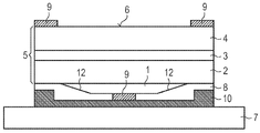
도 1에 도시된 박막-발광 다이오드 칩은 반도체 층 시퀀스(5)를 포함하는데, 상기 층 시퀀스는 p-타입 반도체 영역(2) 및 n-타입 반도체 영역(4)을 포함한다. 상기 p-타입 반도체 영역(2)과 상기 n-타입 반도체 영역(4) 사이에는 활성층(3)이 배치되어 있다. 상기 활성층(3)은 바람직하게 단일-양자 웰 구조물 또는 다중-양자 웰 구조물을 구비한다.The thin film-emitting diode chip shown in FIG. 1 includes a
반도체 층 시퀀스(5)는 포스파이드-화합물 반도체를 기본으로 하는데, 다시 말하자면 상기 반도체 층 시퀀스(5) 안에 포함된 반도체 층들은 특히 InxGayAl1 -x-yP(0 ≤ x ≤ 1이고, 0 ≤ y ≤ 1이며, 그리고 x + y ≤ 1)를 구비한다. 특히 상기 p-타입 반도체 영역(2), 상기 활성층(3) 그리고 상기 n-타입 반도체 영역(4)은 포스파이드 화합물 반도체 재료로부터 형성되었다.The
발광 다이오드 칩으로서는 소위 박막-LED가 사용되며, 상기 박막-LED에서는 반도체 층 시퀀스(5)의 에피택셜 성장을 위해서 사용되는 성장 기판이 상기 반도체 층 시퀀스(5)로부터 분리되었다. 특히 상기 성장 기판은 발광 다이오드 칩의 방사선 배출 면(6)을 구비하는 n-타입 반도체 영역(4)으로부터 분리될 수 있다. 원래의 성장 기판 및 방사선 배출 면(6)에 마주 놓인 한 측에서는 상기 발광 다이오드 칩이 바람직하게 규소, 게르마늄 또는 몰리브덴을 구비하는 캐리어(7)에 연결되어 있다. 따라서, 이와 같은 박막-발광 다이오드 칩의 경우에는 상기 n-타입 반도체 영역(4)이 방사선 배출 면(6) 쪽을 향하고 있고, 상기 p-타입 반도체 영역(2)은 캐리어(7) 쪽을 향하고 있다.As the light emitting diode chip, a so-called thin film-LED is used, in which the growth substrate used for epitaxial growth of the
상기 캐리어(7)와 상기 p-타입-포스파이드 화합물 반도체 영역(2) 사이에는 전류 확산 층(1)이 배치되어 있다. 상기 전류 확산 층(1)은 두께가 500 nm 미만이고 p-도핑 된 하나의 AlxGa1 - xAs-층(이때 0.5 < x ≤ 1)이다.A current spreading
바람직하게 상기 전류 확산 층(1)의 두께는 심지어 겨우 300 nm 미만이다. 상기 전류 확산 층(1) 내부에서의 알루미늄 비율에 대해서는 바람직하게 0.6 ≤ x ≤ 0.8이 적용된다.Preferably the thickness of the current spreading
상기 전류 확산 층(1)은 상기 캐리어(7) 쪽을 향하고 있는 한 측에서는 적어도 부분 영역들에서 전기 콘택(9)에 인접한다. 발광 다이오드 칩의 적어도 하나의 추가 전기 콘택(9)은 예를 들어 캐리어에 마주 놓인 상기 발광 다이오드 칩의 방사선 배출 면(6)에 배치되어 있다. 상기 전류 확산 층(1)은 바람직하게 1 x 1019 cm-3 초과의 도펀트 농도를 가지며, 그리고 특히 바람직하게는 5 x 1019 cm-3 초과의 도펀트 농도를 갖는다. 이와 같은 방식으로 상기 전류 확산 층(1)의 높은 분로 전도성(shunt conductability)이 성취됨으로써, 결과적으로 예를 들어 후방 콘택(9)이 상기 전류 확산 층(1)의 크기가 작은 중앙 영역 상에만 제공된 경우에도 전류는 상기 반도체 층 시퀀스(5)를 비교적 균일하게 관류하게 된다.The current spreading
상기 전류 확산 층(1)은 500 nm 미만의 또는 바람직하게는 300 nm 미만의 얇은 자체 두께 그리고 0.5 초과의 높은 알루미늄-함량으로 인해 바람직하게 낮은 광학적 흡수력을 갖는다. 또한, 상기와 같이 얇은 전류 확산 층(1)은 통상적으로 1 ㎛ 또는 그 이상의 두께를 갖는 비교적 두꺼운 종래의 전류 확산 층들보다 산화 또는 습기 작용에 대하여 덜 민감하다는 사실도 드러났다. 두께가 얇음에도 상기와 같은 전류 확산 층(1)에 의해서는 우수한 전류 확산이 성취되며, 이때에는 상기 전류 확산 층(1)이 적어도 1 x 1019 cm-3의 도펀트 농도를 갖는 경우, 그리고 특히 바람직하게는 적어도 5 x 1019 cm-3의 도펀트 농도를 갖는 경우가 바람직하다.The current spreading
또한, 상기 p-타입 반도체 영역(2)에 인접하는 전류 확산 층(1)이 상기 캐리어(7)와 상기 p-타입 반도체 영역(2) 사이에 배치되어 있는 것도 바람직한데, 그 이유는 이와 같은 배열 상태에서는 상기 전류 확산 층이 발광 다이오드 칩의 표면에서 주변 환경 매체에 인접하게 되는 경우보다 더 우수하게 산화 또는 습기 작용과 같은 외부 영향들에 대하여 보호되기 때문이다.It is also preferable that a current spreading
상기 전류 확산 층(1)은 AlxGa1 -xAs(이때 0.5 < x ≤ 1)로 이루어진 다수의 부분 층으로 구성될 수 있으며, 이 경우 상기 부분 층들은 예를 들어 도펀트 농도 및/또는 알루미늄 함량과 관련하여 서로 구별될 수 있다. 이 경우에 본 출원서의 틀 안에서는 전체 부분 층이 전류 확산 층(1)으로 간주 됨으로써, 결과적으로 특히 모든 부분 층의 총 두께는 500 nm 미만, 그리고 바람직하게는 300 nm 미만이 된다. 전류 확산 층(1) 또는 상기 전류 확산 층의 부분 층들이 소량의 추가 물질을 함유하는 것도 생각할 수 있으나, 이 경우 상기 추가 물질의 총 비율은 10 % 미만에 달한다.The current spreading
전류 확산 층(1)을 외부 영향들로부터 더욱 우수하게 보호하기 위하여, 상기 전류 확산 층 그리고 이 전류 확산 층의 측면(11)에는 바람직하게 캡슐화 층(8)이 제공되었다. 상기 캡슐화 층(8)은 특히 예를 들어 질화 규소 또는 산화 규소와 같은 투명한 유전성 재료를 구비할 수 있다. 그러나 대안적으로는 상기 캡슐화 층(8)이 예를 들어 산화 아연 또는 금속과 같은 투명한 전도성 산화물을 구비하는 경우도 가능하다. 특히 유전성 재료로 이루어진 캡슐화 층(8)의 경우에는, 상기 전류 확산 층(1)을 위한 전기 콘택(9)이 상기 캡슐화 층(8)의 한 리세스 안에 배치될 수 있다.In order to better protect the current spreading
상기 캡슐화 층(8), 상기 전기 콘택 층(9)과 상기 캐리어(7) 사이에는 금속 또는 금속 합금으로 이루어진 층 시퀀스(10)가 배치되어 있다. 상기 금속 층(10)은 예를 들어 활성층(3)으로부터 캐리어(7)의 방향으로 방출되는 방사선을 반사시키기 위한 미러 층을 포함할 수 있다. 또한, 상기 금속 층(10)은 상기 캐리어(7)와 발광 다이오드 칩을 연결하기 위한 납땜 층도 구비할 수 있다.Between the
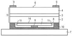
도 2에 도시된 발광 다이오드 칩의 실시 예는 상기 전류 확산 층(1)이 비스듬한 측면(12)을 갖는다는 점에서 도 1에 도시된 실시 예와 상이하다. 상기 비스듬한 측면(12)은 바람직하게 상기 전류 확산 층(1)의 층 평면과 20°(20° 포함) 내지 70°(70° 포함)의 각을 형성한다. 상기 전류 확산 층(1)의 비스듬한 측면(12)에 의해서는 발광 다이오드 칩으로부터의 방사선 외광 효율이 개선될 수 있다고 밝혀졌다. 상기 전류 확산 층(1)과 상기 캡슐화 층(8) 간의 굴절률 차이로 인해 상기 비스듬한 측면(12)은 방사선을 상기 방사선 배출 면(6) 쪽의 방향으로 반사할 수 있는 반사체로서 작용을 한다. 특히 상기 전류 확산 층(1)의 서로 마주 놓인 비스듬한 측면(12)들이 하나의 마이크로프리즘을 형성하는 것이 가능해진다. 또한, 상기 비스듬한 측면(12)들이 반도체 층 시퀀스(5) 내부까지 연장될 수도 있다(도면에는 도시되어 있지 않음).The embodiment of the light emitting diode chip shown in FIG. 2 differs from the embodiment shown in FIG. 1 in that the current spreading
상기 추가의 바람직한 형상들과 관련해서 도 2에 도시된 실시 예는 제 1 실시 예와 일치한다.The embodiment shown in FIG. 2 with respect to said further preferred shapes is consistent with the first embodiment.
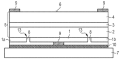
도 3에 도시된 발광 다이오드 칩의 실시 예는 상기 금속 층 시퀀스(10)가 발광 다이오드 칩의 측면 영역에서 상기 p-타입 반도체 영역(2)에까지 근접한다는 점에서 도 1에 도시된 실시 예와 구별된다. 따라서, 상기 전류 확산 층(1) 그리고 이 층의 측면(11)은 캡슐화 층(8)에 의해 둘러싸이며, 그리고 상기 캡슐화 층(8)은 금속 층 시퀀스(10)에 의해서 둘러싸인다. 이와 같은 방식에 의해서 산화 또는 습기 작용에 대한 상기 전류 확산 층(1)의 특히 우수한 안정성이 성취된다.The embodiment of the light emitting diode chip shown in FIG. 3 is distinguished from the embodiment shown in FIG. 1 in that the
도 3에 도시된 실시 예는 상기 전류 확산 층(1)에 InxGayAl1 -x- yAs-층(14)(이때 0 ≤ x ≤ 1이고, 0 ≤ y ≤ 1이며, 그리고 x + y ≤ 1)이 인접하고, 이 층이 상기 전류 확산 층(1)보다 더 낮은 도펀트 농도 및 더 작은 밴드 갭을 갖는다는 점에서 또한 도 1에 도시된 실시 예와 구별된다. 상기 층(14)은 바람직하게 전류 확산 층(1)과 상기 p-타입 반도체 영역(2) 사이에 배치되어 있다. 상기 층(14)은 더 높게 도핑 된 전류 확산 층(1)에 대한 경계면에서 하나의 전위 공동부(potential cavity)를 형성하고, 상기 전위 공동부 안에는 정공의 형태로 형성된 자유로운 전하 캐리어들이 수집된다. 정공은 상기 층(14) 내부에서 소위 2차원적인 정공 가스를 형성한다. 이와 같은 방식에 의해 상기 층(14) 내부에서는 특히 높은 분로 전도성이 성취된다.The embodiment shown in Figure 3 is an In x Ga y Al 1 -x- y As- layer 14 (where 0 ≤ x ≤ 1 to the current diffusion layer (1), and 0 ≤ y ≤ 1, and x It is also distinguished from the embodiment shown in FIG. 1 in that + y ≤ 1) is adjacent and this layer has a lower dopant concentration and a smaller band gap than the current spreading
도 4에 도시된 발광 다이오드 칩의 실시 예에서는 상기 전류 확산 층(1) 내부에 두 개의 트렌치(13)가 형성되며, 상기 트렌치 안으로 캡슐화 층(8)이 돌출한다. 트렌치(13)들 사이에 배치된 상기 전류 확산 층(1)의 영역은 전기 콘택(9)에 의해서 금속 층 시퀀스(10)에 전기적으로 접속되어 있다. 그와 달리 상기 전류 확산 층(1)의 가장자리 영역(1a, 1b)은 전기적으로 접속되어 있지 않다. 이와 같은 방식에 의해서는, 상기 가장자리 영역들 안에 배치된 콘택(9) 아래에서 발광 다이오드 칩의 방사선 배출 면 상에 배치된 반도체 칩의 영역들 안에서 방사선이 발생할 가능성이 줄어든다.In the embodiment of the light emitting diode chip shown in FIG. 4, two
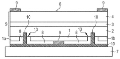
도 5에는 상기 전류 확산 층(1) 안에 두 개의 트렌치(13)가 형성된 발광 다이오드 칩의 한 가지 추가 실시 예가 도시되어 있다. 상기 트렌치들 안에서는 금속 층 시퀀스(10)가 상기 p-타입 반도체 영역(2) 내부까지 연장된다. 상기 금속 층 시퀀스(10)는 상기 콘택(9) 영역 외부에서 상기 캡슐화 층(8)에 의해 전류 확산 층(1)으로부터 절연되어 있다.5 shows one further embodiment of a light emitting diode chip in which two
본 출원서에 기재된 발명은 실시 예들을 참조한 설명에 의해서 한정되지 않는다. 오히려 본 발명은 각각의 새로운 특징 그리고 각각의 특징 조합을 포함하며, 이 경우 특히 각각의 특징 조합은 이와 같은 특징 또는 특징 조합 자체가 특허청구범위 또는 실시 예에 명시적으로 기재되어 있지 않더라도 특허청구범위에 포함된 것으로 간주 된다.The invention described in this application is not limited by the description with reference to the embodiments. Rather, the present invention includes each novel feature and each feature combination, in which case each feature combination, whether such feature or feature combination per se is not explicitly recited in the claims or embodiments, Are considered to be included.
Claims (15)
상기 반도체 층 시퀀스(5)가
p-타입 반도체 영역(2),
n-타입 반도체 영역(4), 그리고
상기 p-타입 반도체 영역(2)과 상기 n-타입 반도체 영역(4) 사이에 배치되어 있고 전자기 방사선을 방출하기 위한 활성층(3)
을 포함하며,
이때 상기 n-타입 반도체 영역(4)은 발광 다이오드 칩의 방사선 배출 면(6) 쪽을 향하고 있으며, 그리고 상기 p-타입 반도체 영역(2)은 발광 다이오드 칩의 캐리어(7) 쪽을 향하고 있고,
상기 캐리어(7)와 상기 p-타입 반도체 영역(2) 사이에는 두께가 500 nm 미만인 전류 확산 층(1)이 배치되어 있으며, 상기 전류 확산 층은 하나 또는 다수의 p-도핑 된 AlxGa1 - xAs-층을 구비하며, 이때 0.5 < x ≤ 1인,
발광 다이오드 칩.A light emitting diode chip having a semiconductor layer sequence (5) comprising a phosphide compound semiconductor material,
The semiconductor layer sequence 5
p-type semiconductor region (2),
n-type semiconductor region 4, and
An active layer 3 disposed between the p-type semiconductor region 2 and the n-type semiconductor region 4 and for emitting electromagnetic radiation
/ RTI >
At this time, the n-type semiconductor region 4 faces the radiation emitting surface 6 side of the LED chip, and the p-type semiconductor region 2 faces the carrier 7 side of the LED chip,
A current spreading layer 1 having a thickness of less than 500 nm is disposed between the carrier 7 and the p-type semiconductor region 2, wherein the current spreading layer is one or multiple p-doped Al x Ga 1. with x As-layer, wherein 0.5 <x ≤ 1,
Light emitting diode chip.
상기 전류 확산 층(1)의 두께가 300 nm 미만인,
발광 다이오드 칩.The method of claim 1,
The thickness of the current spreading layer 1 is less than 300 nm,
Light emitting diode chip.
상기 전류 확산 층(1)의 알루미늄 비율(x)이 0.6 ≤ x ≤ 0.8인,
발광 다이오드 칩.3. The method according to claim 1 or 2,
The aluminum ratio x of the current spreading layer 1 is 0.6 ≦ x ≦ 0.8,
Light emitting diode chip.
상기 전류 확산 층(1)이 1 * 1019 cm-3 초과의 도펀트 농도를 갖는,
발광 다이오드 칩.The method according to any one of claims 1 to 3,
The current spreading layer 1 has a dopant concentration of greater than 1 * 10 19 cm -3 ,
Light emitting diode chip.
상기 전류 확산 층(1)이 적어도 5 * 1019 cm-3의 도펀트 농도를 갖는,
발광 다이오드 칩.The method according to any one of claims 1 to 4,
The current spreading layer 1 has a dopant concentration of at least 5 * 10 19 cm -3 ,
Light emitting diode chip.
상기 전류 확산 층(1)이 C로 도핑되는,
발광 다이오드 칩.6. The method according to any one of claims 1 to 5,
The current spreading layer 1 is doped with C,
Light emitting diode chip.
상기 전류 확산 층(1) 및 상기 전류 확산 층의 측면(11)에 캡슐화 층(8)이 제공되는,
발광 다이오드 칩.7. The method according to any one of claims 1 to 6,
On the current spreading layer 1 and on the side 11 of the current spreading layer an encapsulation layer 8 is provided,
Light emitting diode chip.
상기 캡슐화 층(8)이 산화 규소, 질화 규소, 산화 아연 또는 금속을 함유하는,
발광 다이오드 칩.The method of claim 7, wherein
The encapsulation layer 8 contains silicon oxide, silicon nitride, zinc oxide or a metal,
Light emitting diode chip.
상기 전류 확산 층(1)이 비스듬한 측면(12)을 가지며, 상기 비스듬한 측면은 상기 전류 확산 층(1)의 층 평면에 대하여 20°(20° 포함) 내지 70°(70° 포함)의 각만큼 기울어져 있는,
발광 다이오드 칩.The method according to any one of claims 1 to 8,
The current spreading layer 1 has an oblique side 12, which is at an angle of 20 ° (including 20 °) to 70 ° (including 70 °) with respect to the layer plane of the current spreading layer 1. Tilted,
Light emitting diode chip.
상기 전류 확산 층(1) 안에 적어도 하나의 트렌치(13)가 형성된,
발광 다이오드 칩.10. The method according to any one of claims 1 to 9,
At least one trench 13 is formed in the current spreading layer 1,
Light emitting diode chip.
상기 적어도 하나의 트렌치(13)가 질화 규소, 산화 규소, 산화 아연 또는 금속으로 채워진,
발광 다이오드 칩.11. The method of claim 10,
Wherein the at least one trench 13 is filled with silicon nitride, silicon oxide, zinc oxide or a metal,
Light emitting diode chip.
상기 적어도 하나의 트렌치(13)가 상기 p-타입 반도체 영역(2) 내부까지 연장되는,
발광 다이오드 칩.The method of claim 10 or 11,
The at least one trench 13 extends into the p-type semiconductor region 2,
Light emitting diode chip.
InxGayAl1 -x- yAs(0 ≤ x ≤ 1이고, 0 ≤ y ≤ 1이며, 그리고 x + y ≤ 1)로 이루어진 적어도 하나의 층이 상기 전류 확산 층(1)에 인접하며, 상기 층은 전류 확산 층(1)보다 더 작은 밴드 갭 및 더 낮은 도펀트 농도를 갖는,
발광 다이오드 칩.13. The method according to any one of claims 1 to 12,
In x Ga y Al 1 -x- y As the at least one layer made of (and 0 ≤ x ≤ 1, and 0 ≤ y ≤ 1, and x + y ≤ 1) adjacent to the current diffusion layer (1), and Wherein the layer has a smaller band gap and lower dopant concentration than the current spreading layer (1),
Light emitting diode chip.
성장 기판은 상기 반도체 층 시퀀스(5)로부터 분리되어 있으며, 그리고 상기 캐리어(7)는 상기 반도체 층 시퀀스(5)의 성장 기판과 상이한,
발광 다이오드 칩.14. The method according to any one of claims 1 to 13,
The growth substrate is separated from the semiconductor layer sequence 5, and the carrier 7 is different from the growth substrate of the semiconductor layer sequence 5,
Light emitting diode chip.
상기 캐리어(7)가 규소, 몰리브덴 또는 게르마늄을 구비하는,
발광 다이오드 칩.15. The method of claim 14,
The carrier 7 comprises silicon, molybdenum or germanium,
Light emitting diode chip.
Applications Claiming Priority (3)
| Application Number | Priority Date | Filing Date | Title |
|---|---|---|---|
| DE102010014667A DE102010014667A1 (en) | 2010-04-12 | 2010-04-12 | LED chip with current spreading layer |
| DE102010014667.6 | 2010-04-12 | ||
| PCT/EP2011/055566 WO2011128277A1 (en) | 2010-04-12 | 2011-04-08 | Light-emitting diode chip with current spreading layer |
Publications (1)
| Publication Number | Publication Date |
|---|---|
| KR20130060189A true KR20130060189A (en) | 2013-06-07 |
Family
ID=44123194
Family Applications (1)
| Application Number | Title | Priority Date | Filing Date |
|---|---|---|---|
| KR1020127029623A KR20130060189A (en) | 2010-04-12 | 2011-04-08 | Light-emitting diode chip with current spreading layer |
Country Status (7)
| Country | Link |
|---|---|
| US (2) | US20130126920A1 (en) |
| EP (2) | EP3131127B1 (en) |
| JP (2) | JP5943904B2 (en) |
| KR (1) | KR20130060189A (en) |
| CN (2) | CN105206731B (en) |
| DE (1) | DE102010014667A1 (en) |
| WO (1) | WO2011128277A1 (en) |
Cited By (4)
| Publication number | Priority date | Publication date | Assignee | Title |
|---|---|---|---|---|
| WO2021183415A1 (en) * | 2020-03-11 | 2021-09-16 | Lumileds Llc | Light emitting diode devices with current spreading layer |
| WO2021183411A1 (en) * | 2020-03-11 | 2021-09-16 | Lumileds Llc | Light emitting diode devices with common electrode |
| WO2021183413A1 (en) * | 2020-03-11 | 2021-09-16 | Lumileds Llc | Light emitting diode devices with multilayer composite film including current spreading layer |
| WO2021183414A1 (en) * | 2020-03-11 | 2021-09-16 | Lumileds Llc | Light emitting diode devices with defined hard mask opening |
Families Citing this family (11)
| Publication number | Priority date | Publication date | Assignee | Title |
|---|---|---|---|---|
| DE102010014667A1 (en) * | 2010-04-12 | 2011-10-13 | Osram Opto Semiconductors Gmbh | LED chip with current spreading layer |
| DE102013100818B4 (en) | 2013-01-28 | 2023-07-27 | OSRAM Opto Semiconductors Gesellschaft mit beschränkter Haftung | Optoelectronic semiconductor chip and method for producing an optoelectronic semiconductor chip |
| EP2903027B1 (en) * | 2014-01-30 | 2018-08-22 | AZUR SPACE Solar Power GmbH | LED semiconductor component |
| JP2016054260A (en) | 2014-09-04 | 2016-04-14 | 株式会社東芝 | Semiconductor light-emitting element |
| DE102015011635B4 (en) | 2015-09-11 | 2020-10-08 | Azur Space Solar Power Gmbh | Infrared LED |
| DE102015118041A1 (en) | 2015-10-22 | 2017-04-27 | Osram Opto Semiconductors Gmbh | Light-emitting diode chip and method for producing a light-emitting diode chip |
| DE102017101637A1 (en) | 2017-01-27 | 2018-08-02 | Osram Opto Semiconductors Gmbh | Optoelectronic semiconductor chip |
| DE102017104144B9 (en) * | 2017-02-28 | 2022-03-10 | OSRAM Opto Semiconductors Gesellschaft mit beschränkter Haftung | Process for the production of light-emitting diodes |
| TWI635626B (en) * | 2017-10-19 | 2018-09-11 | 友達光電股份有限公司 | Light emitting apparatus |
| US11942507B2 (en) | 2020-03-11 | 2024-03-26 | Lumileds Llc | Light emitting diode devices |
| CN116978999B (en) * | 2023-09-22 | 2024-01-02 | 南昌凯捷半导体科技有限公司 | Current-limited Micro-LED chip and manufacturing method thereof |
Family Cites Families (36)
| Publication number | Priority date | Publication date | Assignee | Title |
|---|---|---|---|---|
| JPS51149784A (en) | 1975-06-17 | 1976-12-22 | Matsushita Electric Ind Co Ltd | Solid state light emission device |
| JPS52124885A (en) | 1976-04-12 | 1977-10-20 | Matsushita Electric Ind Co Ltd | Semiconductor light emitting device |
| NZ201460A (en) | 1981-08-17 | 1986-11-12 | Allware Agencies Ltd | Multipurpose microprocessor controlled heating and cooling fan |
| US4901330A (en) * | 1988-07-20 | 1990-02-13 | Amoco Corporation | Optically pumped laser |
| JP3290672B2 (en) | 1990-08-20 | 2002-06-10 | 株式会社東芝 | Semiconductor light emitting diode |
| JPH07307489A (en) | 1994-05-13 | 1995-11-21 | Toshiba Corp | Semiconductor light-emitting element and its manufacture |
| JP3797748B2 (en) | 1997-05-30 | 2006-07-19 | シャープ株式会社 | Light emitting diode array |
| JP2000101133A (en) | 1998-09-21 | 2000-04-07 | Hitachi Cable Ltd | Epitaxial wafer for light-emitting element and manufacture thereof |
| JP3881470B2 (en) | 1999-01-05 | 2007-02-14 | ローム株式会社 | Manufacturing method of semiconductor light emitting device |
| JP2000307185A (en) | 1999-04-20 | 2000-11-02 | Rohm Co Ltd | Semiconductor light emitting element and its manufacture |
| JP2001077411A (en) | 1999-08-31 | 2001-03-23 | Oki Electric Ind Co Ltd | Light-emitting diode array and manufacture thereof |
| US6424669B1 (en) * | 1999-10-29 | 2002-07-23 | E20 Communications, Inc. | Integrated optically pumped vertical cavity surface emitting laser |
| JP4773597B2 (en) | 1999-12-24 | 2011-09-14 | ローム株式会社 | Semiconductor light emitting device |
| US20020017652A1 (en) | 2000-08-08 | 2002-02-14 | Stefan Illek | Semiconductor chip for optoelectronics |
| JP2002190619A (en) | 2000-12-22 | 2002-07-05 | Toshiba Corp | Semiconductor light-emitting element and its manufacturing method |
| JP3814151B2 (en) * | 2001-01-31 | 2006-08-23 | 信越半導体株式会社 | Light emitting element |
| US6555405B2 (en) * | 2001-03-22 | 2003-04-29 | Uni Light Technology, Inc. | Method for forming a semiconductor device having a metal substrate |
| US6618418B2 (en) * | 2001-11-15 | 2003-09-09 | Xerox Corporation | Dual III-V nitride laser structure with reduced thermal cross-talk |
| US20040021142A1 (en) | 2002-07-30 | 2004-02-05 | Li-Hsin Kuo | Light emitting diode device |
| US7041529B2 (en) * | 2002-10-23 | 2006-05-09 | Shin-Etsu Handotai Co., Ltd. | Light-emitting device and method of fabricating the same |
| JP2004281559A (en) * | 2003-03-13 | 2004-10-07 | Toshiba Corp | Semiconductor light emitting device |
| JP3788444B2 (en) * | 2003-03-31 | 2006-06-21 | 日立電線株式会社 | Light emitting diode and manufacturing method thereof |
| JP4178410B2 (en) | 2003-11-26 | 2008-11-12 | サンケン電気株式会社 | Semiconductor light emitting device |
| JP2005276899A (en) | 2004-03-23 | 2005-10-06 | Shin Etsu Handotai Co Ltd | Light-emitting element |
| US7512167B2 (en) * | 2004-09-24 | 2009-03-31 | Sanyo Electric Co., Ltd. | Integrated semiconductor laser device and method of fabricating the same |
| DE102005029272A1 (en) * | 2005-03-31 | 2006-10-12 | Osram Opto Semiconductors Gmbh | Radiation-emitting semiconductor chip for data communications has electrical connection that is either laterally apart from injection section or overlaps injection and isolation sections |
| JP4830356B2 (en) | 2005-06-08 | 2011-12-07 | ソニー株式会社 | Semiconductor light emitting device and semiconductor light emitting device |
| US7368759B2 (en) * | 2005-09-30 | 2008-05-06 | Hitachi Cable, Ltd. | Semiconductor light-emitting device |
| JP4320653B2 (en) | 2005-09-30 | 2009-08-26 | 日立電線株式会社 | Semiconductor light emitting device |
| JP2007103725A (en) | 2005-10-05 | 2007-04-19 | Toshiba Corp | Semiconductor light emitting device |
| KR100849826B1 (en) * | 2007-03-29 | 2008-07-31 | 삼성전기주식회사 | Light emitting device and package including the same |
| DE102007022947B4 (en) * | 2007-04-26 | 2022-05-05 | OSRAM Opto Semiconductors Gesellschaft mit beschränkter Haftung | Optoelectronic semiconductor body and method for producing such |
| DE102007023878A1 (en) * | 2007-05-23 | 2008-11-27 | Osram Opto Semiconductors Gmbh | Semiconductor chip and method for producing a semiconductor chip |
| KR100891761B1 (en) * | 2007-10-19 | 2009-04-07 | 삼성전기주식회사 | Semiconductor light emitting device, manufacturing method thereof and semiconductor light emitting device package using the same |
| DE102008010296A1 (en) * | 2007-11-30 | 2009-06-04 | Osram Opto Semiconductors Gmbh | LED i.e. thin film LED, has spreading layer joined to coating layer, where spreading layer contains aluminum and exhibits refractive index, which is larger than refractive index of adjacent coating layers |
| DE102010014667A1 (en) * | 2010-04-12 | 2011-10-13 | Osram Opto Semiconductors Gmbh | LED chip with current spreading layer |
-
2010
- 2010-04-12 DE DE102010014667A patent/DE102010014667A1/en not_active Withdrawn
-
2011
- 2011-04-08 JP JP2013504213A patent/JP5943904B2/en active Active
- 2011-04-08 CN CN201510504954.0A patent/CN105206731B/en active Active
- 2011-04-08 KR KR1020127029623A patent/KR20130060189A/en not_active Application Discontinuation
- 2011-04-08 US US13/640,037 patent/US20130126920A1/en not_active Abandoned
- 2011-04-08 WO PCT/EP2011/055566 patent/WO2011128277A1/en active Application Filing
- 2011-04-08 EP EP16181773.9A patent/EP3131127B1/en active Active
- 2011-04-08 EP EP11714027.7A patent/EP2559076B1/en active Active
- 2011-04-08 CN CN201180018587.3A patent/CN102834937B/en active Active
-
2015
- 2015-08-19 US US14/830,616 patent/US9853188B2/en active Active
- 2015-10-20 JP JP2015206284A patent/JP6124973B2/en active Active
Cited By (8)
| Publication number | Priority date | Publication date | Assignee | Title |
|---|---|---|---|---|
| WO2021183415A1 (en) * | 2020-03-11 | 2021-09-16 | Lumileds Llc | Light emitting diode devices with current spreading layer |
| WO2021183411A1 (en) * | 2020-03-11 | 2021-09-16 | Lumileds Llc | Light emitting diode devices with common electrode |
| WO2021183413A1 (en) * | 2020-03-11 | 2021-09-16 | Lumileds Llc | Light emitting diode devices with multilayer composite film including current spreading layer |
| WO2021183414A1 (en) * | 2020-03-11 | 2021-09-16 | Lumileds Llc | Light emitting diode devices with defined hard mask opening |
| US11569415B2 (en) | 2020-03-11 | 2023-01-31 | Lumileds Llc | Light emitting diode devices with defined hard mask opening |
| US11735695B2 (en) | 2020-03-11 | 2023-08-22 | Lumileds Llc | Light emitting diode devices with current spreading layer |
| US11784286B2 (en) | 2020-03-11 | 2023-10-10 | Lumileds Llc | Light emitting diode devices with defined hard mask opening |
| US11848402B2 (en) | 2020-03-11 | 2023-12-19 | Lumileds Llc | Light emitting diode devices with multilayer composite film including current spreading layer |
Also Published As
| Publication number | Publication date |
|---|---|
| CN105206731B (en) | 2018-01-19 |
| CN105206731A (en) | 2015-12-30 |
| EP3131127B1 (en) | 2018-01-31 |
| JP2013524547A (en) | 2013-06-17 |
| EP2559076B1 (en) | 2016-09-21 |
| JP2016048785A (en) | 2016-04-07 |
| WO2011128277A1 (en) | 2011-10-20 |
| JP5943904B2 (en) | 2016-07-05 |
| CN102834937B (en) | 2015-08-26 |
| EP2559076A1 (en) | 2013-02-20 |
| EP3131127A1 (en) | 2017-02-15 |
| US20130126920A1 (en) | 2013-05-23 |
| CN102834937A (en) | 2012-12-19 |
| JP6124973B2 (en) | 2017-05-10 |
| US20150357516A1 (en) | 2015-12-10 |
| US9853188B2 (en) | 2017-12-26 |
| DE102010014667A1 (en) | 2011-10-13 |
Similar Documents
| Publication | Publication Date | Title |
|---|---|---|
| US9853188B2 (en) | Light-emitting diode chip with current spreading layer | |
| US10043958B2 (en) | Light emitting diode chip | |
| US8928052B2 (en) | Optoelectronic semiconductor chip and method for producing same | |
| US9799797B2 (en) | Light-emitting semiconductor chip | |
| US10304998B2 (en) | Light emitting diode chip and light emitting device having the same | |
| US9299897B2 (en) | Optoelectronic semiconductor chip having a plurality of active regions arranged alongside one another | |
| KR101634410B1 (en) | Optoelectronic semiconductor body | |
| KR101475963B1 (en) | Radiation emitting semiconductor body having an electrically conductive contact layer permeable to the emitted radiation | |
| US9214595B2 (en) | Semiconductor light emitting device | |
| JP6924836B2 (en) | Optoelectronic semiconductor chip | |
| US8115219B2 (en) | LED semiconductor body and use of an LED semiconductor body | |
| KR20100072277A (en) | Thin-film led having a mirror layer and method for the production thereof | |
| JP2011505073A (en) | Optoelectronic semiconductor body and method of manufacturing optoelectronic semiconductor body | |
| US7470934B2 (en) | Radiation-emitting optoelectronic semiconductor chip with a diffusion barrier | |
| JP2019511844A (en) | Optoelectronics semiconductor chip | |
| US10263143B2 (en) | Semiconductor chip | |
| KR20230128361A (en) | Optoelectronic semiconductor component with a gold layer in the edge region | |
| KR102100937B1 (en) | Light Emitting Diode Chip having recessed pattern |
Legal Events
| Date | Code | Title | Description |
|---|---|---|---|
| WITN | Application deemed withdrawn, e.g. because no request for examination was filed or no examination fee was paid |