KR20130008100A - Organic light emitting diode lighting apparatus - Google Patents
Organic light emitting diode lighting apparatus Download PDFInfo
- Publication number
- KR20130008100A KR20130008100A KR1020110060883A KR20110060883A KR20130008100A KR 20130008100 A KR20130008100 A KR 20130008100A KR 1020110060883 A KR1020110060883 A KR 1020110060883A KR 20110060883 A KR20110060883 A KR 20110060883A KR 20130008100 A KR20130008100 A KR 20130008100A
- Authority
- KR
- South Korea
- Prior art keywords
- light emitting
- thickness
- organic light
- thickness portion
- emitting element
- Prior art date
Links
- 239000000758 substrate Substances 0.000 claims abstract description 16
- 238000005538 encapsulation Methods 0.000 claims description 17
- 239000011521 glass Substances 0.000 claims description 8
- 229910052751 metal Inorganic materials 0.000 claims description 7
- 239000002184 metal Substances 0.000 claims description 7
- 239000000463 material Substances 0.000 claims description 4
- 239000007769 metal material Substances 0.000 claims description 3
- 238000000034 method Methods 0.000 claims 5
- 238000002347 injection Methods 0.000 description 11
- 239000007924 injection Substances 0.000 description 11
- 230000000694 effects Effects 0.000 description 8
- 238000007789 sealing Methods 0.000 description 8
- 230000017525 heat dissipation Effects 0.000 description 6
- 239000011575 calcium Substances 0.000 description 2
- 239000011651 chromium Substances 0.000 description 2
- 239000010931 gold Substances 0.000 description 2
- 238000002834 transmittance Methods 0.000 description 2
- OYPRJOBELJOOCE-UHFFFAOYSA-N Calcium Chemical compound [Ca] OYPRJOBELJOOCE-UHFFFAOYSA-N 0.000 description 1
- VYZAMTAEIAYCRO-UHFFFAOYSA-N Chromium Chemical compound [Cr] VYZAMTAEIAYCRO-UHFFFAOYSA-N 0.000 description 1
- WHXSMMKQMYFTQS-UHFFFAOYSA-N Lithium Chemical compound [Li] WHXSMMKQMYFTQS-UHFFFAOYSA-N 0.000 description 1
- 229910000861 Mg alloy Inorganic materials 0.000 description 1
- BQCADISMDOOEFD-UHFFFAOYSA-N Silver Chemical compound [Ag] BQCADISMDOOEFD-UHFFFAOYSA-N 0.000 description 1
- XLOMVQKBTHCTTD-UHFFFAOYSA-N Zinc monoxide Chemical compound [Zn]=O XLOMVQKBTHCTTD-UHFFFAOYSA-N 0.000 description 1
- 229910052782 aluminium Inorganic materials 0.000 description 1
- XAGFODPZIPBFFR-UHFFFAOYSA-N aluminium Chemical compound [Al] XAGFODPZIPBFFR-UHFFFAOYSA-N 0.000 description 1
- 229910052791 calcium Inorganic materials 0.000 description 1
- 239000000919 ceramic Substances 0.000 description 1
- 229910052804 chromium Inorganic materials 0.000 description 1
- 230000007423 decrease Effects 0.000 description 1
- 238000005516 engineering process Methods 0.000 description 1
- PCHJSUWPFVWCPO-UHFFFAOYSA-N gold Chemical compound [Au] PCHJSUWPFVWCPO-UHFFFAOYSA-N 0.000 description 1
- 229910052737 gold Inorganic materials 0.000 description 1
- 230000005283 ground state Effects 0.000 description 1
- 230000005525 hole transport Effects 0.000 description 1
- 238000005286 illumination Methods 0.000 description 1
- 229910003437 indium oxide Inorganic materials 0.000 description 1
- PJXISJQVUVHSOJ-UHFFFAOYSA-N indium(iii) oxide Chemical compound [O-2].[O-2].[O-2].[In+3].[In+3] PJXISJQVUVHSOJ-UHFFFAOYSA-N 0.000 description 1
- AMGQUBHHOARCQH-UHFFFAOYSA-N indium;oxotin Chemical compound [In].[Sn]=O AMGQUBHHOARCQH-UHFFFAOYSA-N 0.000 description 1
- 229910052744 lithium Inorganic materials 0.000 description 1
- 239000011777 magnesium Substances 0.000 description 1
- 239000012528 membrane Substances 0.000 description 1
- 150000002739 metals Chemical class 0.000 description 1
- 238000012986 modification Methods 0.000 description 1
- 230000004048 modification Effects 0.000 description 1
- 239000010453 quartz Substances 0.000 description 1
- 230000000191 radiation effect Effects 0.000 description 1
- 239000000565 sealant Substances 0.000 description 1
- 238000000926 separation method Methods 0.000 description 1
- VYPSYNLAJGMNEJ-UHFFFAOYSA-N silicon dioxide Inorganic materials O=[Si]=O VYPSYNLAJGMNEJ-UHFFFAOYSA-N 0.000 description 1
- 229910052709 silver Inorganic materials 0.000 description 1
- 239000004332 silver Substances 0.000 description 1
- YVTHLONGBIQYBO-UHFFFAOYSA-N zinc indium(3+) oxygen(2-) Chemical compound [O--].[Zn++].[In+3] YVTHLONGBIQYBO-UHFFFAOYSA-N 0.000 description 1
Images


Classifications
-
- H—ELECTRICITY
- H10—SEMICONDUCTOR DEVICES; ELECTRIC SOLID-STATE DEVICES NOT OTHERWISE PROVIDED FOR
- H10K—ORGANIC ELECTRIC SOLID-STATE DEVICES
- H10K59/00—Integrated devices, or assemblies of multiple devices, comprising at least one organic light-emitting element covered by group H10K50/00
- H10K59/80—Constructional details
- H10K59/87—Passivation; Containers; Encapsulations
- H10K59/871—Self-supporting sealing arrangements
-
- H—ELECTRICITY
- H10—SEMICONDUCTOR DEVICES; ELECTRIC SOLID-STATE DEVICES NOT OTHERWISE PROVIDED FOR
- H10K—ORGANIC ELECTRIC SOLID-STATE DEVICES
- H10K50/00—Organic light-emitting devices
- H10K50/80—Constructional details
- H10K50/84—Passivation; Containers; Encapsulations
- H10K50/841—Self-supporting sealing arrangements
-
- H—ELECTRICITY
- H10—SEMICONDUCTOR DEVICES; ELECTRIC SOLID-STATE DEVICES NOT OTHERWISE PROVIDED FOR
- H10K—ORGANIC ELECTRIC SOLID-STATE DEVICES
- H10K59/00—Integrated devices, or assemblies of multiple devices, comprising at least one organic light-emitting element covered by group H10K50/00
- H10K59/80—Constructional details
- H10K59/87—Passivation; Containers; Encapsulations
- H10K59/871—Self-supporting sealing arrangements
- H10K59/8721—Metallic sealing arrangements
-
- H—ELECTRICITY
- H10—SEMICONDUCTOR DEVICES; ELECTRIC SOLID-STATE DEVICES NOT OTHERWISE PROVIDED FOR
- H10K—ORGANIC ELECTRIC SOLID-STATE DEVICES
- H10K2102/00—Constructional details relating to the organic devices covered by this subclass
- H10K2102/301—Details of OLEDs
- H10K2102/351—Thickness
-
- H—ELECTRICITY
- H10—SEMICONDUCTOR DEVICES; ELECTRIC SOLID-STATE DEVICES NOT OTHERWISE PROVIDED FOR
- H10K—ORGANIC ELECTRIC SOLID-STATE DEVICES
- H10K50/00—Organic light-emitting devices
- H10K50/80—Constructional details
- H10K50/84—Passivation; Containers; Encapsulations
- H10K50/842—Containers
- H10K50/8423—Metallic sealing arrangements
-
- Y—GENERAL TAGGING OF NEW TECHNOLOGICAL DEVELOPMENTS; GENERAL TAGGING OF CROSS-SECTIONAL TECHNOLOGIES SPANNING OVER SEVERAL SECTIONS OF THE IPC; TECHNICAL SUBJECTS COVERED BY FORMER USPC CROSS-REFERENCE ART COLLECTIONS [XRACs] AND DIGESTS
- Y02—TECHNOLOGIES OR APPLICATIONS FOR MITIGATION OR ADAPTATION AGAINST CLIMATE CHANGE
- Y02B—CLIMATE CHANGE MITIGATION TECHNOLOGIES RELATED TO BUILDINGS, e.g. HOUSING, HOUSE APPLIANCES OR RELATED END-USER APPLICATIONS
- Y02B20/00—Energy efficient lighting technologies, e.g. halogen lamps or gas discharge lamps
- Y02B20/30—Semiconductor lamps, e.g. solid state lamps [SSL] light emitting diodes [LED] or organic LED [OLED]
Landscapes
- Physics & Mathematics (AREA)
- Optics & Photonics (AREA)
- Electroluminescent Light Sources (AREA)
Abstract
Description
본 발명의 실시예는 조명 장치에 관한 것으로, 보다 상세하게는 유기 발광 소자를 이용한 유기 발광 조명 장치에 관한 것이다.Embodiment of the present invention relates to a lighting device, and more particularly to an organic light emitting lighting device using an organic light emitting device.
유기 발광 조명 장치는 유기 발광 소자가 방출하는 빛을 이용하는 조명 장치이다. 유기 발광 소자(organic light emitting diode, OLED)는 유기 발광층 내부에서 전자와 정공이 결합하여 형성된 여기자(exciton)가 기저 상태로 떨어질 때 발생하는 에너지에 의해 빛을 발생시킨다.The organic light emitting lighting device is a lighting device using light emitted by the organic light emitting device. An organic light emitting diode (OLED) generates light by energy generated when an exciton formed by combining electrons and holes in an organic light emitting layer falls to a ground state.
유기 발광 조명 장치는 단순히 빛을 발생시킬 수 있으면 되므로, 유기 발광 소자를 이용한 표시 장치와 비교하여 상대적으로 간소한 구조를 가질 수 있다.The organic light emitting lighting device may simply generate light, and thus may have a relatively simple structure compared to the display device using the organic light emitting device.
한편, 유기 발광 조명 장치도, 단순히 빛을 방출하는 것 이외에, 기능적 또는 심미적인 필요에 따라 간단한 이미지를 표시할 수 있는 표시 기능이 요구되고 있다.On the other hand, in addition to simply emitting light, organic light-emitting lighting apparatuses require a display function capable of displaying a simple image according to their functional or aesthetic needs.
하지만, 유기 발광 조명 장치가 표시 기능을 갖기 위해서는 구조가 복잡해지는 문제점이 있다.However, there is a problem that the structure is complicated in order for the organic light emitting lighting device to have a display function.
본 발명의 실시예는 간소한 구조를 가지면서 동시에 유기 발광 소자가 방출하는 빛의 휘도 편차를 이용한 표시 기능을 갖는 유기 발광 조명 장치를 제공한다.An embodiment of the present invention provides an organic light emitting lighting device having a simple structure and at the same time having a display function using the luminance deviation of the light emitted by the organic light emitting device.
본 발명의 실시예에 따르면, 유기 발광 조명 장치는 기판 본체와, 상기 기판 본체 상에 형성된 유기 발광 소자, 그리고 상기 기판 본체와 합착되어 상기 유기 발광 소자를 밀봉 커버하는 봉지캔을 포함한다. 또한, 상기 봉지캔은 상기 유기 발광 소자와 대향하는 면이 서로 다른 두께를 갖는 복수의 두께부들로 구분된다.According to an embodiment of the present invention, the organic light emitting diode lighting apparatus includes a substrate body, an organic light emitting element formed on the substrate body, and an encapsulation can which is bonded to the substrate body to seal and cover the organic light emitting element. In addition, the encapsulation can is divided into a plurality of thickness parts having different thicknesses from surfaces facing the organic light emitting element.
상기 복수의 두께부들은 제1 두께부와, 상기 제1 두께부보다 얇은 두께를 갖는 제2 두께부를 포함할 수 있다.The plurality of thickness parts may include a first thickness part and a second thickness part having a thickness thinner than the first thickness part.
상기 제2 두께부는 상기 제1 두께부보다 상기 유기 발광 소자와 상대적으로 멀리 이격될 수 있다.The second thickness portion may be relatively far from the organic light emitting element than the first thickness portion.
상기 제2 두께부와 대응하는 상기 유기 발광 소자가 상기 제1 두께부와 대응하는 상기 유기 발광 소자보다 상대적으로 높은 휘도의 빛을 방출할 수 있다.The organic light emitting diode corresponding to the second thickness portion may emit light having a higher luminance than the organic light emitting diode corresponding to the first thickness portion.
상기 제1 두께부의 두께와 상기 제2 두께부의 두께 간의 차이는 100㎛ 보다 크거나 같을 수 있다.The difference between the thickness of the first thickness portion and the thickness of the second thickness portion may be greater than or equal to 100 μm.
상기 제1 두께부는 300㎛ 내지 600㎛ 범위 내의 두께를 가지며, 상기 제2 두께부는 200㎛ 내지 500㎛ 범위 내의 두께를 가질 수 있다.The first thickness portion may have a thickness in the range of 300 μm to 600 μm, and the second thickness portion may have a thickness in the range of 200 μm to 500 μm.
상기 봉지캔의 전체 두께는 400㎛ 내지 900㎛ 범위 내의 두께를 가질 수 있다.The entire thickness of the encapsulation can may have a thickness in the range of 400 μm to 900 μm.
상기 봉지캔의 제2 두께부는 상기 유기 발광 소자와 대향하는 면의 일부가 함몰 형성될 수 있다.A portion of a surface of the encapsulating can facing the organic light emitting element may be recessed.
상기한 유기 발광 조명 장치에서, 상기 봉지캔은 금속 소재로 형성된 메탈캔(metal can) 및 글라스 소재로 만들어진 글라스캔(glass can) 중 하나일 수 있다.In the above organic light emitting lighting device, the encapsulation can may be one of a metal can formed of a metal material and a glass can made of a glass material.
상기 제2 두께부는 숫자, 문자, 및 기호 중 하나 이상을 포함하는 도형으로 형성될 수 있다.The second thickness portion may be formed as a figure including one or more of numbers, letters, and symbols.
상기 유기 발광 소자가 방출하는 빛의 휘도는 1000nit 보다 크거나 같을 수 있다.The luminance of light emitted from the organic light emitting diode may be greater than or equal to 1000 nits.
본 발명의 실시예에 따르면, 유기 발광 조명 장치는 간소한 구조를 가지면서 동시에 유기 발광 소자가 방출하는 빛의 휘도 편차를 이용한 표시 기능을 가질 수 있다.According to the exemplary embodiment of the present invention, the organic light emitting lighting device may have a simple structure and at the same time have a display function using a luminance deviation of light emitted by the organic light emitting element.
도 1은 본 발명의 일 실시예에 따른 유기 발광 조명 장치의 단면도이다.
도 2는 도 1의 유기 발광 조명 장치의 봉지캔의 배면 사시도이다.
도 3 및 도 4는 본 발명의 일 실시예에 따른 실험예를 나타낸 사진이다.1 is a cross-sectional view of an organic light emitting lighting device according to an embodiment of the present invention.
FIG. 2 is a rear perspective view of a sealing can of the organic light emitting illuminator of FIG. 1.
3 and 4 are photographs showing an experimental example according to an embodiment of the present invention.
이하, 첨부한 도면을 참고로 하여 본 발명의 실시예에 대하여 본 발명이 속하는 기술 분야에서 통상의 지식을 가진 자가 용이하게 실시할 수 있도록 상세히 설명한다. 본 발명은 여러 가지 상이한 형태로 구현될 수 있으며 여기에서 설명하는 실시예에 한정되지 않는다.Hereinafter, exemplary embodiments of the present invention will be described in detail with reference to the accompanying drawings so that those skilled in the art may easily implement the present invention. The present invention may be embodied in many different forms and is not limited to the embodiments described herein.
또한, 명세서 전체를 통하여 동일 또는 유사한 구성 요소에 대해서는 동일한 참조 부호를 붙이도록 한다.Also, like reference numerals designate like elements throughout the specification.
또한, 도면에서 나타난 각 구성의 크기 및 두께는 설명의 편의를 위해 임의로 나타내었으므로, 본 발명이 반드시 도시된 바에 한정되지 않는다.In addition, since the sizes and thicknesses of the respective components shown in the drawings are arbitrarily shown for convenience of explanation, the present invention is not necessarily limited to those shown in the drawings.
도면에서 여러 층 및 영역을 명확하게 표현하기 위하여 두께를 확대하여 나타내었다. 그리고 도면에서, 설명의 편의를 위해, 일부 층 및 영역의 두께를 과장되게 나타내었다. 층, 막, 영역, 판 등의 부분이 다른 부분 "위에" 또는 "상에" 있다고 할 때, 이는 다른 부분 "바로 위에" 있는 경우뿐 아니라 그 중간에 또 다른 부분이 있는 경우도 포함한다.In the drawings, the thickness is enlarged to clearly represent the layers and regions. In the drawings, for the convenience of explanation, the thicknesses of some layers and regions are exaggerated. Whenever a portion such as a layer, film, region, plate, or the like is referred to as being "on" or "on" another portion, it includes not only the case where it is "directly on" another portion but also the case where there is another portion in between.
이하, 도 1 및 도 2를 참조하여 본 발명의 일 실시예에 따른 유기 발광 조명 장치(101)를 설명한다.Hereinafter, an organic light
도 1에 도시한 바와 같이, 본 발명의 일 실시예에 따른 유기 발광 조명 장치(101)는 기판 본체(111), 유기 발광 소자(70), 및 봉지캔(200)을 포함한다. 그리고 도시하지는 않았으나, 유기 발광 조명 장치(101)는 기판 본체(111)와 봉지캔(200)을 서로 합착시키는 실런트를 더 포함할 수 있다.As shown in FIG. 1, the organic light emitting
기판 본체(111)는 유리, 석영, 및 세라믹 등으로 만들어진 투명한 절연성 기판으로 형성되거나, 플라스틱 등으로 만들어진 투명한 플렉서블(flexible) 기판으로 형성될 수 있다.The substrate
유기 발광 소자(70)는 제1 전극(710), 유기 발광층(720), 및 제2 전극(720)을 포함한다.The organic
제1 전극(710)은 정공 주입 전극인 양(+)극이 된다. 그리고 제2 전극(730)이 전자 주입 전극인 음(-)극이 된다. 하지만, 본 발명의 일 실시예가 이에 한정되는 것은 아니다. 따라서, 제1 전극(710)이 전자 주입 전극이 되고, 제2 전극(730)이 정공 주입 전극이 될 수도 있다.The
또한, 제1 전극(710)은 투명 도전막 또는 반투과막으로 형성되고, 제2 전극(730)은 반사막으로 형성된다.In addition, the
투명 도전막은 ITO(Indium Tin Oxide), IZO(Indium Zinc Oxide), ZnO(산화 아연) 또는 In2O3(Indium Oxide) 등의 물질을 사용하여 만들어진다. 이러한 투명 도전막은 상대적으로 높은 일함수를 갖는다. 따라서, 투명 도전막으로 형성된 제1 전극(710)은 정공 주입을 원활하게 수행할 수 있다. 또한, 제1 전극(710)이 투명 도전막으로 형성될 경우, 유기 발광 조명 장치(101)는 제1 전극(710)의 상대적으로 높은 비저항을 보완하기 위해 상대적으로 비저항이 낮은 금속으로 만들어진 보조 전극을 더 포함할 수 있다.The transparent conductive film is made of a material such as indium tin oxide (ITO), indium zinc oxide (IZO), zinc oxide (ZnO), or indium oxide (In 2 O 3 ). Such a transparent conductive film has a relatively high work function. Therefore, the
반사막 및 반투과막은 마그네슘(Mg), 은(Ag), 금(Au), 칼슘(Ca), 리튬(Li), 크롬(Cr), 및 알루미늄(Al) 중 하나 이상의 금속 또는 이들의 합금을 사용하여 만들어진다. 이때, 반사막과 반투과막은 두께로 결정된다. 일반적으로, 반투과막은 200nm 이하의 두께를 갖는다. 반투과막은 두께가 얇아질수록 빛의 투과율이 높아지고, 두께가 두꺼워질수록 빛의 투과율이 낮아진다.The reflective film and the semi-transmissive film use one or more metals or alloys of magnesium (Mg), silver (Ag), gold (Au), calcium (Ca), lithium (Li), chromium (Cr), and aluminum (Al). Is made. At this time, the reflective film and the semi-transmissive film are determined by the thickness. In general, the transflective film has a thickness of 200 nm or less. As the thickness of the semi-permeable membrane becomes thinner, the light transmittance increases, and as the thickness becomes thicker, the light transmittance decreases.
제1 전극(710)이 반투과 전극으로 형성되고 제2 전극(730)이 반사막으로 형성될 경우, 마이크로캐비티(microcavity) 효과를 이용해 빛의 이용 효율을 향상시킬 수 있다.When the
또한, 제1 전극(710)이 투명 도전막과 반투과막을 포함하는 다중막 구조로 형성될 수도 있다. 이 경우, 제1 전극(710)이 높은 일함수를 가지면서 동시에 마이크로캐비티 효과를 얻을 수 있다.In addition, the
유기 발광층(720)은 발광층과, 정공 주입층(hole-injection layer, HIL), 정공 수송층(hole-transporting layer, HTL), 전자 수송층(electron-transportiong layer, ETL), 및 전자 주입층(electron-injection layer, EIL) 중 하나 이상을 포함하는 다중막으로 형성된다. 전술한 층들 중에 발광층을 제외한 나머지 층들은 필요에 따라 생략될 수 있다. 유기 발광층(720)이 전술한 모든 층들을 포함할 경우, 정공 주입층이 정공 주입 전극인 제1 전극(710) 상에 배치되고, 그 위로 정공 수송층, 발광층, 전자 수송층, 전자 주입층이 차례로 적층된다. 또한, 유기 발광층(720)은 필요에 따라 다른 층을 더 포함할 수도 있다.The organic
또한, 유기 발광 소자(720)는 최소 1000nit(cd/m2) 이상의 휘도를 갖는 빛을 방출한다.In addition, the organic
이와 같이, 본 발명의 일 실시예에 따른 유기 발광 조명 장치(101)는 유기 발광층(720)에서 발생된 빛이 제1 전극(710) 및 기판 본체(111)를 통과해 외부로 방출되는 배면 발광형 구조를 갖는다.As described above, the organic light
봉지캔(200)은 기판 본체(111)와 합착되어 유기 발광 소자(70)를 밀봉 커버한다. 봉지캔(200)은, 도 1 및 도 2에 도시한 바와 같이, 유기 발광 소자(70)와 대향하는 면이 서로 다른 두께를 갖는 복수의 두께부들(201, 202)로 구분된다.The encapsulation can 200 is bonded to the substrate
구체적으로, 본 발명의 일 실시예에서, 복수의 두께부들은 제1 두께부(201)와 제2 두께부(202)를 포함한다. 하지만, 본 발명의 일 실시예가 이에 한정되는 것은 아니다. 따라서 봉지캔(200)의 서로 다른 두께를 갖는 셋 이상의 두께부들을 포함할 수도 있다.Specifically, in one embodiment of the present invention, the plurality of thickness portions includes a
그리고 제2 두께부(202)는 제1 두께부(201)보다 100㎛ 이상 얇은 두께를 갖는다. 즉, 제1 두께부(201)와 제2 두께부(202)의 두께 차이(t3)는 100㎛ 이상이다. 또한, 제2 두께부(202)는 제1 두께부(201) 보다 유기 발광 소자(70)와 상대적으로 멀리 이격된다. 즉, 봉지캔(200)의 유기 발광 소자(70)와 대향하는 면의 일부가 함몰되어 제2 두께부(202)가 된다.The
제2 두께부(202)는 숫자, 문자, 및 기호 중 하나 이상을 포함하는 도형(圖形)으로 형성된다. 여기서, 기호는 다각형, 원형, 및 각종 형상 등을 포함한다.The
제2 두께부(202)는 제1 두께부(201) 보다 얇은 두께를 가지므로, 상대적으로 방열 효과가 적다. 따라서, 제2 두께부(202)와 대응하는 유기 발광 소자(70)는 제1 두께부(201)와 대응하는 유기 발광 소자(70) 보다 상대적으로 높은 온도를 갖게 된다. 그리고 제2 두께부(202)와 대응하는 유기 발광 소자(70)가 제1 두께부(201)와 대응하는 유기 발광 소자(70) 보다 높은 휘도의 빛을 방출하게 된다. 이는 유기 발광 소자(70)의 특성상 온도가 올라가면 전압이 낮아지기 때문이다. 따라서, 제1 두께부(201)와 제2 두께부(202)의 두께 차이에 의한 유기 발광 소자(70)의 휘도 편차와 제2 두께부(202)가 갖는 모양을 이용하여 유기 발광 조명 장치(101)는 간단한 이미지를 표시할 수 있다.Since the
또한, 일례로, 제1 두께부(201)는 300㎛ 내지 600㎛ 범위 내의 두께(t1)를 가지며, 제2 두께부(202)는 200㎛ 내지 500㎛ 범위 내의 두께(t2)를 가질 수 있다. 그리고 봉지캔(200)의 전체 두께(t4)는 400㎛ 내지 900㎛ 범위 내에 속한다.Also, as an example, the
제1 두께부(201)가 300㎛ 작으면, 방열 효과가 지나치게 낮아지고 유기 발광 소자(70)를 보호하기 위한 충분한 강도를 갖지 못한다. 반면, 제1 두께부(201)가 600㎛보다 두꺼우면, 유기 발광 조명 장치(200)의 전체적인 두께가 불필요하게 두꺼워진다.When the
제2 두께부(202)의 두께(t2)는 제1 두께부(201)와 100㎛ 이상의 차이를 두고 설정된다. 그리고 봉지캔(200)의 전체 두께(t4)는 제1 두께부(201)의 두께(t1) 및 제1 두께부(201)와 유기 발광 소자 사이(70)의 이격 거리를 고려하여 설정된다.The thickness t2 of the
이와 같은 구성에 의하여, 본 발명의 일 실시예에 따른 유기 발광 조명 장치(101)는 간소한 구조를 가지면서 동시에 유기 발광 소자(70)가 방출하는 빛의 휘도 차이를 이용한 표시 기능을 가질 수 있다.By such a configuration, the organic light emitting
구체적으로, 봉지캔(200)의 제1 두께부(201)와 제2 두께부(202) 간의 두께 차이에 의해, 유기 발광 소자(70)에 휘도 편차가 발생한다. 그리고, 제2 두께부(202)를 숫자, 문자, 및 기호 등을 포함하는 도형으로 형성하고, 유기 발광 소자(70)의 휘도 편차를 이용하여 간단한 이미지를 표시할 수 있다. 즉, 제2 두께부(202)의 모양이 곧 유기 발광 조명 장치(101)가 표시하는 이미지가 된다.Specifically, the luminance difference occurs in the organic
한편, 봉지캔(200)의 제1 두께부(201)와 제2 두께부(202) 간의 두께 차이가 100㎛ 미만이면 방열 효과에 따른 휘도 편차가 미미해진다. 따라서, 유기 발광 조명 장치(101)가 효과적으로 이미지를 표시하기 위해서는 제1 두께부(201)와 제2 두께부(202) 간의 두께 차이가 100㎛ 이상이어야 한다.On the other hand, if the thickness difference between the
또한, 봉지캔(200)은 금속 소재로 만들어진 메탈캔(metal can) 및 글라스 소재로 만들어진 글라스캔(glass can) 중 하나일 수 있다. 메탈캔이 봉지캔(200)으로 사용된 경우 방열 효과가 더 우수하나, 글라스캔이 봉지캔(200)으로 사용된 경우에도 본 발명의 일 실시예에 따르면 방열 효과를 극대화할 수 있다.In addition, the encapsulation can 200 may be one of a metal can made of a metal material and a glass can made of a glass material. When the metal can is used as the encapsulation can 200, the heat dissipation effect is better, but even when the glass can is used as the encapsulation can 200, the heat dissipation effect can be maximized.
또한, 본 발명의 일 실시예에 따르면, 유기 발광 조명 장치(101)는 기설정된 휘도 이상의 빛을 방출할 때 이미지가 표시될 수 있다. 유기 발광 소자(70)의 특성상 유기 발광 소자(70)가 방출하는 빛이 1000nit 미만이면, 유기 발광 소자(70)의 발열량이 적어 봉지캔(200)의 제1 두께부(201)와 제2 두께부(202) 간의 방열 효과 차이의 영향을 덜 받는다. 즉, 유기 발광 소자(70)의 전체적인 온도 편차가 상대적으로 약해진다. 따라서, 제2 두께부(202)와 대응하는 유기 발광 소자(70)와 제1 두께부(201)와 대응하는 유기 발광 소자(70) 간의 휘도 편차도 미미해진다. 반면, 유기 발광 소자(70)가 방출하는 빛의 휘도가 1000nit 이상이 되면, 유기 발광 소자(70)가 상대적으로 높은 열을 방출하게 된다. 따라서, 봉지캔(200)의 제1 두께부(201)와 제2 두께부(202) 간의 방열 효과 차이의 영향받아 유기 발광 소자(70)의 전체적인 온도 편차가 상대적으로 강해진다. 이에, 제2 두께부(202)와 대응하는 유기 발광 소자(70)와 제1 두께부(201)와 대응하는 유기 발광 소자(70) 간의 휘도 편차가 발생되고, 유기 발광 조명 장치(101)는 이를 이용해 이미지를 표시할 수 있다.In addition, according to an embodiment of the present invention, the organic light emitting
이와 같이, 유기 발광 조명 장치(101)는 단순히 이미지를 표시할 수 있는 것 뿐만 아니라, 특정 휘도 영역에서만 이미지를 표시할 수 있다.As such, the organic light emitting
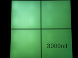
이하, 도 3 및 도 4를 참조하여 본 발명의 일 실시예에 따른 실험예를 살펴본다. 실험예는 본 발명의 일 실시예에 따른, 도 2에 도시한 바와 같은, 봉지캔(200)을 사용하고 있다. 여기서, 봉지캔(200)은 메탈캔이 사용되었다. 도 3은 평균적으로 3000nit의 휘도를 갖는 빛을 방출하는 실험예를 나타내고, 도 4는 평균적으로 500nit의 휘도를 갖는 빛을 방출하는 실험예를 나타낸다.Hereinafter, an experimental example according to an embodiment of the present invention will be described with reference to FIGS. 3 and 4. Experimental example uses a bag can 200, as shown in Figure 2, according to an embodiment of the present invention. Here, the metal can is used for the sealing can 200. 3 shows an experimental example of emitting light having an average luminance of 3000 nits, and FIG. 4 shows an experimental example of emitting light having an average luminance of 500 nits.
도 3에 도시한 바와 같이, 본 발명의 일 실시예에 따른 실험예가 평균적으로 3000nit의 휘도를 갖는 빛을 방출할 때, 봉지캔(200)의 제2 두께부(202)(도 2에 도시)와 같은 형상의 이미지가 표시됨을 알 수 있다.As shown in FIG. 3, when the experimental example according to the embodiment of the present invention emits light having a luminance of 3000 nit on average, the second thickness portion 202 (shown in FIG. 2) of the bag can 200. It can be seen that the image of the shape as shown.
반변, 도 4에 도시한 바와 같이, 본 발명의 일 실시예에 따른 실험예가 평균적으로 500nit의 휘도를 갖는 빛을 방출할 때, 이미지가 표시되지 않음을 알 수 있다.On the other hand, as shown in Figure 4, it can be seen that when the experimental example according to an embodiment of the present invention emits light having a luminance of 500 nit on average, the image is not displayed.
이와 같은 설험을 통해, 본 발명의 일 실시예에 따른 유기 발광 조명 장치(101)는 간소한 구조를 가지고 유기 발광 소자(70)가 방출하는 빛의 휘도 차이를 이용한 이미지 표시가 가능할 뿐만 아니라, 특정 휘도 영역에서만 이미지를 표시할 수 있음을 알 수 있었다.Through such a description, the organic light emitting
본 발명을 앞서 기재한 바에 따라 바람직한 실시예를 통해 설명하였지만, 본 발명은 이에 한정되지 않으며 다음에 기재하는 특허청구범위의 개념과 범위를 벗어나지 않는 한, 다양한 수정 및 변형이 가능하다는 것을 본 발명이 속하는 기술 분야에 종사하는 자들은 쉽게 이해할 것이다.While the invention has been shown and described with reference to certain preferred embodiments thereof, it will be understood by those skilled in the art that various changes and modifications may be made therein without departing from the spirit and scope of the following claims. Those who are engaged in the technology field will understand easily.
70: 유기 발광 소자 101: 유기 발광 조명 장치
111: 기판 본체 200: 봉지캔70: organic light emitting element 101: organic light emitting illumination device
111: substrate body 200: sealing can
Claims (11)
상기 기판 본체 상에 형성된 유기 발광 소자; 그리고
상기 기판 본체와 합착되어 상기 유기 발광 소자를 밀봉 커버하는 봉지캔
을 포함하며,
상기 봉지캔은 상기 유기 발광 소자와 대향하는 면이 서로 다른 두께를 갖는 복수의 두께부들로 구분된 유기 발광 조명 장치.A substrate body;
An organic light emitting element formed on the substrate main body; And
An encapsulation can attached to the substrate main body to seal and cover the organic light emitting device.
/ RTI >
The encapsulation can is divided into a plurality of thickness parts having different thicknesses on surfaces facing the organic light emitting element.
상기 복수의 두께부들은 제1 두께부와, 상기 제1 두께부보다 얇은 두께를 갖는 제2 두께부를 포함하는 유기 발광 조명 장치.In claim 1,
The plurality of thickness parts may include a first thickness part and a second thickness part having a thickness thinner than the first thickness part.
상기 제2 두께부는 상기 제1 두께부보다 상기 유기 발광 소자와 상대적으로 멀리 이격된 유기 발광 조명 장치.In claim 2,
And the second thickness part is relatively far from the organic light emitting element than the first thickness part.
상기 제2 두께부와 대응하는 상기 유기 발광 소자가 상기 제1 두께부와 대응하는 상기 유기 발광 소자보다 상대적으로 높은 휘도의 빛을 방출하는 유기 발광 조명 장치.In claim 2,
And the organic light emitting element corresponding to the second thickness portion emits light having a higher luminance than the organic light emitting element corresponding to the first thickness portion.
상기 제1 두께부의 두께와 상기 제2 두께부의 두께 간의 차이는 100㎛ 보다 크거나 같은 유기 발광 조명 장치.In claim 2,
And a difference between the thickness of the first thickness portion and the thickness of the second thickness portion is greater than or equal to 100 μm.
상기 제1 두께부는 300㎛ 내지 600㎛ 범위 내의 두께를 가지며,
상기 제2 두께부는 200㎛ 내지 500㎛ 범위 내의 두께를 갖는 유기 발광 조명 장치.The method of claim 5,
The first thickness portion has a thickness in the range of 300 ㎛ to 600 ㎛,
And the second thickness portion has a thickness within a range of 200 μm to 500 μm.
상기 봉지캔의 전체 두께는 400㎛ 내지 900㎛ 범위 내의 두께를 갖는 유기 발광 조명 장치.The method of claim 6,
The organic light emitting device of the encapsulation can has a thickness in the range of 400㎛ to 900㎛.
상기 봉지캔의 제2 두께부는 상기 유기 발광 소자와 대향하는 면의 일부가 함몰 형성된 유기 발광 조명 장치.In claim 1,
And a second thickness portion of the encapsulating can in which a part of a surface facing the organic light emitting element is recessed.
상기 봉지캔은 금속 소재로 형성된 메탈캔(metal can) 및 글라스 소재로 만들어진 글라스캔(glass can) 중 하나인 유기 발광 조명 장치.9. The method according to any one of claims 1 to 8,
The encapsulating can is one of a metal can formed of a metal material and a glass can made of a glass material.
상기 제2 두께부는 숫자, 문자, 및 기호 중 하나 이상을 포함하는 도형으로 형성된 유기 발광 조명 장치.The method of claim 9,
And the second thickness portion is formed as a figure including one or more of numbers, letters, and symbols.
상기 유기 발광 소자가 방출하는 빛의 휘도는 1000nit 보다 크거나 같은 유기 발광 조명 장치.11. The method of claim 10,
The luminance of light emitted by the organic light emitting device is greater than or equal to 1000 nit.
Priority Applications (3)
| Application Number | Priority Date | Filing Date | Title |
|---|---|---|---|
| KR1020110060883A KR20130008100A (en) | 2011-06-22 | 2011-06-22 | Organic light emitting diode lighting apparatus |
| US13/452,539 US20120326204A1 (en) | 2011-06-22 | 2012-04-20 | Organic light emitting diode lighting apparatus |
| DE102012210381A DE102012210381A1 (en) | 2011-06-22 | 2012-06-20 | Organic light emitting diodes lighting device |
Applications Claiming Priority (1)
| Application Number | Priority Date | Filing Date | Title |
|---|---|---|---|
| KR1020110060883A KR20130008100A (en) | 2011-06-22 | 2011-06-22 | Organic light emitting diode lighting apparatus |
Publications (1)
| Publication Number | Publication Date |
|---|---|
| KR20130008100A true KR20130008100A (en) | 2013-01-22 |
Family
ID=47321540
Family Applications (1)
| Application Number | Title | Priority Date | Filing Date |
|---|---|---|---|
| KR1020110060883A KR20130008100A (en) | 2011-06-22 | 2011-06-22 | Organic light emitting diode lighting apparatus |
Country Status (3)
| Country | Link |
|---|---|
| US (1) | US20120326204A1 (en) |
| KR (1) | KR20130008100A (en) |
| DE (1) | DE102012210381A1 (en) |
Cited By (2)
| Publication number | Priority date | Publication date | Assignee | Title |
|---|---|---|---|---|
| KR20170001578U (en) | 2015-10-27 | 2017-05-10 | 동우 화인켐 주식회사 | Back plane and organic light emitting diode having the same |
| KR20170001576U (en) | 2015-10-27 | 2017-05-10 | 동우 화인켐 주식회사 | Back plane and organic light emitting diode having the same |
Family Cites Families (12)
| Publication number | Priority date | Publication date | Assignee | Title |
|---|---|---|---|---|
| CA2394645A1 (en) * | 1999-06-11 | 2000-12-21 | Sydney Hyman | Image making medium |
| US7255823B1 (en) * | 2000-09-06 | 2007-08-14 | Institute Of Materials Research And Engineering | Encapsulation for oled devices |
| TWI237725B (en) * | 2002-01-23 | 2005-08-11 | Sony Corp | Image display device and image projector device |
| JP2004241695A (en) * | 2003-02-07 | 2004-08-26 | Seiko Epson Corp | Manufacturing method of optical device |
| US20040189195A1 (en) * | 2003-03-24 | 2004-09-30 | Osram Opto Semiconductors Gmbh | Devices including, methods using, and compositions of reflowable getters |
| JP4511440B2 (en) * | 2004-10-05 | 2010-07-28 | 三星モバイルディスプレイ株式會社 | ORGANIC LIGHT EMITTING ELEMENT AND METHOD FOR PRODUCING ORGANIC LIGHT EMITTING ELEMENT |
| KR100670328B1 (en) * | 2005-03-30 | 2007-01-16 | 삼성에스디아이 주식회사 | Organic light-emitting display and manufacturing method thereof |
| US20070013293A1 (en) * | 2005-07-12 | 2007-01-18 | Eastman Kodak Company | OLED device having spacers |
| US7582508B2 (en) * | 2006-05-31 | 2009-09-01 | Byoung-Choo Park | Method for manufacturing an organic semiconductor device that utilizes ionic salt |
| KR101107158B1 (en) * | 2009-07-10 | 2012-01-25 | 삼성모바일디스플레이주식회사 | Organic light emitting diode display and method for manufacturing the same |
| KR101097344B1 (en) * | 2010-03-09 | 2011-12-23 | 삼성모바일디스플레이주식회사 | Method of manufacturing flexible display apparatus |
| JP2011257651A (en) * | 2010-06-10 | 2011-12-22 | Canon Inc | Light emitting substrate and image display device having the same |
-
2011
- 2011-06-22 KR KR1020110060883A patent/KR20130008100A/en not_active Application Discontinuation
-
2012
- 2012-04-20 US US13/452,539 patent/US20120326204A1/en not_active Abandoned
- 2012-06-20 DE DE102012210381A patent/DE102012210381A1/en not_active Withdrawn
Cited By (2)
| Publication number | Priority date | Publication date | Assignee | Title |
|---|---|---|---|---|
| KR20170001578U (en) | 2015-10-27 | 2017-05-10 | 동우 화인켐 주식회사 | Back plane and organic light emitting diode having the same |
| KR20170001576U (en) | 2015-10-27 | 2017-05-10 | 동우 화인켐 주식회사 | Back plane and organic light emitting diode having the same |
Also Published As
| Publication number | Publication date |
|---|---|
| US20120326204A1 (en) | 2012-12-27 |
| DE102012210381A1 (en) | 2012-12-27 |
Similar Documents
| Publication | Publication Date | Title |
|---|---|---|
| KR101084246B1 (en) | Organic light emitting diode lighting apparatus | |
| US9356259B2 (en) | Organic light-emitting display apparatus and method of manufacturing the same | |
| JP5335909B2 (en) | Electroluminescent display device, lighting device or display device, and manufacturing process thereof | |
| KR101456154B1 (en) | Organic light emitting diode lighting apparatus | |
| JP5480567B2 (en) | Organic light emitting device | |
| JP2008091323A5 (en) | ||
| TW200714608A (en) | Transition metal complex compound and organic electroluminescent device using the same | |
| JP2009110780A (en) | Organic electroluminescent display panel, and manufacturing method thereof | |
| US20130140982A1 (en) | Organic light emitting display device and manufacturing method thereof | |
| KR20120118335A (en) | Organic light emitting diode lighting apparatus | |
| JP5297399B2 (en) | Light emitting device | |
| KR20130004829A (en) | Organic light emitting diode lighting apparatus | |
| JP2007531297A5 (en) | ||
| KR20110039839A (en) | Organic light emitting diode lighting apparatus and method for manufacturing the same | |
| JP2011204645A (en) | Light-emitting device | |
| JP2004281374A (en) | Top emission light emitting display having reflective layer | |
| KR20110057673A (en) | Organic light emitting diode lighting apparatus | |
| KR101049800B1 (en) | Organic light emitting device | |
| KR20130008100A (en) | Organic light emitting diode lighting apparatus | |
| TWI327042B (en) | Double-sided organic electro-luminescence device and electronic device | |
| CN109244253B (en) | Lighting device using organic light emitting diode | |
| JP5452266B2 (en) | Light emitting device | |
| JP2020120113A5 (en) | ||
| JP4990967B2 (en) | Organic light emitting device unit and method for manufacturing the same | |
| WO2016042921A1 (en) | Light emitting device |
Legal Events
| Date | Code | Title | Description |
|---|---|---|---|
| N231 | Notification of change of applicant | ||
| A201 | Request for examination | ||
| E902 | Notification of reason for refusal | ||
| E601 | Decision to refuse application |