KR20130000292A - 전극 물질 및 이의 제조 방법 - Google Patents
전극 물질 및 이의 제조 방법 Download PDFInfo
- Publication number
- KR20130000292A KR20130000292A KR1020110060902A KR20110060902A KR20130000292A KR 20130000292 A KR20130000292 A KR 20130000292A KR 1020110060902 A KR1020110060902 A KR 1020110060902A KR 20110060902 A KR20110060902 A KR 20110060902A KR 20130000292 A KR20130000292 A KR 20130000292A
- Authority
- KR
- South Korea
- Prior art keywords
- solution
- electrode material
- carbon nanotubes
- conductive polymer
- supernatant
- Prior art date
- Legal status (The legal status is an assumption and is not a legal conclusion. Google has not performed a legal analysis and makes no representation as to the accuracy of the status listed.)
- Granted
Links
Images



Classifications
-
- H—ELECTRICITY
- H01—ELECTRIC ELEMENTS
- H01B—CABLES; CONDUCTORS; INSULATORS; SELECTION OF MATERIALS FOR THEIR CONDUCTIVE, INSULATING OR DIELECTRIC PROPERTIES
- H01B1/00—Conductors or conductive bodies characterised by the conductive materials; Selection of materials as conductors
- H01B1/04—Conductors or conductive bodies characterised by the conductive materials; Selection of materials as conductors mainly consisting of carbon-silicon compounds, carbon or silicon
-
- C—CHEMISTRY; METALLURGY
- C09—DYES; PAINTS; POLISHES; NATURAL RESINS; ADHESIVES; COMPOSITIONS NOT OTHERWISE PROVIDED FOR; APPLICATIONS OF MATERIALS NOT OTHERWISE PROVIDED FOR
- C09D—COATING COMPOSITIONS, e.g. PAINTS, VARNISHES OR LACQUERS; FILLING PASTES; CHEMICAL PAINT OR INK REMOVERS; INKS; CORRECTING FLUIDS; WOODSTAINS; PASTES OR SOLIDS FOR COLOURING OR PRINTING; USE OF MATERIALS THEREFOR
- C09D5/00—Coating compositions, e.g. paints, varnishes or lacquers, characterised by their physical nature or the effects produced; Filling pastes
- C09D5/24—Electrically-conducting paints
-
- H—ELECTRICITY
- H01—ELECTRIC ELEMENTS
- H01B—CABLES; CONDUCTORS; INSULATORS; SELECTION OF MATERIALS FOR THEIR CONDUCTIVE, INSULATING OR DIELECTRIC PROPERTIES
- H01B1/00—Conductors or conductive bodies characterised by the conductive materials; Selection of materials as conductors
- H01B1/06—Conductors or conductive bodies characterised by the conductive materials; Selection of materials as conductors mainly consisting of other non-metallic substances
- H01B1/12—Conductors or conductive bodies characterised by the conductive materials; Selection of materials as conductors mainly consisting of other non-metallic substances organic substances
-
- H—ELECTRICITY
- H01—ELECTRIC ELEMENTS
- H01J—ELECTRIC DISCHARGE TUBES OR DISCHARGE LAMPS
- H01J17/00—Gas-filled discharge tubes with solid cathode
- H01J17/02—Details
- H01J17/04—Electrodes; Screens
-
- H—ELECTRICITY
- H01—ELECTRIC ELEMENTS
- H01M—PROCESSES OR MEANS, e.g. BATTERIES, FOR THE DIRECT CONVERSION OF CHEMICAL ENERGY INTO ELECTRICAL ENERGY
- H01M4/00—Electrodes
- H01M4/02—Electrodes composed of, or comprising, active material
-
- H—ELECTRICITY
- H05—ELECTRIC TECHNIQUES NOT OTHERWISE PROVIDED FOR
- H05K—PRINTED CIRCUITS; CASINGS OR CONSTRUCTIONAL DETAILS OF ELECTRIC APPARATUS; MANUFACTURE OF ASSEMBLAGES OF ELECTRICAL COMPONENTS
- H05K1/00—Printed circuits
- H05K1/02—Details
- H05K1/09—Use of materials for the conductive, e.g. metallic pattern
- H05K1/092—Dispersed materials, e.g. conductive pastes or inks
Landscapes
- Chemical & Material Sciences (AREA)
- Engineering & Computer Science (AREA)
- Microelectronics & Electronic Packaging (AREA)
- Life Sciences & Earth Sciences (AREA)
- Physics & Mathematics (AREA)
- Spectroscopy & Molecular Physics (AREA)
- Dispersion Chemistry (AREA)
- Electrochemistry (AREA)
- Chemical Kinetics & Catalysis (AREA)
- General Chemical & Material Sciences (AREA)
- Materials Engineering (AREA)
- Wood Science & Technology (AREA)
- Organic Chemistry (AREA)
- Manufacturing Of Electric Cables (AREA)
- Conductive Materials (AREA)
- Photovoltaic Devices (AREA)
- Electroluminescent Light Sources (AREA)
Abstract
Description
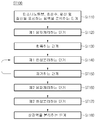
도 2는 상청액을 준비하는 단계의 공정 흐름도이다.
도 3은 PEDOT 및 PSS의 분자 구조를 설명하기 위한 화학식이다.
도 4는 실시예에 따른 전극 물질의 투과도에 대한 그래프이다.
Claims (16)
- 탄소나노튜브 상청액(supernatant)을 준비하는 단계; 및
상기 상청액에 전도성 고분자 용액을 혼합하여 혼합 용액을 형성하는 단계를 포함하는 전극 물질 제조 방법. - 제1항에 있어서,
상기 상청액을 준비하는 단계는,
탄소나노튜브, 초순수, 황산 및 질산을 포함하는 제1 용액을 준비하는 단계; 및
상기 제1 용액을 제1 음파처리(sonication)하는 단계를 포함하는 전극 물질 제조 방법. - 제2항에 있어서,
상기 제1 용액을 환류(reflux)하는 단계를 포함하는 전극 물질 제조 방법. - 제2항 및 제3항 중 어느 하나의 항에 있어서,
상기 제1 용액을 제1 원심분리(centrifuge)하는 단계를 포함하는 전극 물질 제조 방법. - 제4항에 있어서,
상기 제1 원심분리하는 단계 후, 분리된 산성 용액을 제거하는 단계를 포함하는 전극 물질 제조 방법. - 제5항에 있어서,
상기 제1 원심분리하는 단계 및 상기 산성 용액을 제거하는 단계는 적어도 한 번 이상 진행되는 전극 물질 제조 방법. - 제6항에 있어서,
상기 용액을 제2 음파처리하는 단계를 포함하는 전극 물질 제조 방법. - 제7항에 있어서,
상기 용액을 제2 원심분리하는 단계를 포함하는 전극 물질 제조 방법. - 제8항에 있어서,
상기 제2 원심분리하는 단계 후, 상청액을 분리하는 단계를 포함하는 전극 물질 제조 방법. - 제1항에 있어서,
상기 탄소나노튜브는 단일벽 탄소나노튜브를 포함하는 전극 물질 제조 방법. - 제10항에 있어서,
상기 전도성 고분자 용액은, 용매, 전도성 고분자 및 도펀트를 포함하고,
상기 전도성 고분자는 폴리에틸렌디옥시티오펜(Poly(3,4-Ethylenedioxythiophene), PEDOT), 폴리아닐린(polyaniline), 폴리피롤(polypyrrole), 폴리티오펜(polythiophene) 및 이들의 유도체 중 적어도 어느 하나를 포함하는 전극 물질 제조 방법. - 제11항에 있어서,
상기 도펀트는 폴리스티렌술폰산(polystyrene sulfonate, PSS), 도데실벤젠술폰산(Dodecylbenzene sulfonate), 톨루엔술폰산(Toluene sulfonyl), 켐포술폰산, 벤젠술폰산, 염산 및 이들의 유도체 중 적어도 어느 하나를 포함하는 전극 물질 제조 방법. - 제12항에 있어서,
상기 용매는 디메틸설폭사이드(Dimethylsulfoxide,DMSO) 및 엔-메틸피로리돈(N-Methyl-pyrrolidone, NMP) 중 적어도 어느 하나를 포함하는 전극 물질 제조 방법. - 전도성 고분자 및 탄소나노튜브를 포함하고,
상기 탄소나노튜브가 상기 전도성 고분자에 균일하게 분산된 전극 물질. - 제14항에 있어서,
상기 전도성 고분자는 폴리스티렌술폰산(polystyrene sulfonate, PSS) 및 폴리에틸렌디옥시티오펜(Poly(3,4-Ethylenedioxythiophene), PEDOT)을 포함하고,
상기 탄소나노튜브 및 상기 폴리스티렌술폰산이 결합되는 전극 물질. - 제15항에 있어서,
상기 탄소나노튜브 및 상기 폴리스티렌술폰산이 파이-겹침 상호작용(pi-pi stacking interactions)하는 전극 물질.
Priority Applications (1)
| Application Number | Priority Date | Filing Date | Title |
|---|---|---|---|
| KR1020110060902A KR101856778B1 (ko) | 2011-06-22 | 2011-06-22 | 전극 물질, 전극 물질의 제조 방법 및 이를 이용한 전극 제조 방법 |
Applications Claiming Priority (1)
| Application Number | Priority Date | Filing Date | Title |
|---|---|---|---|
| KR1020110060902A KR101856778B1 (ko) | 2011-06-22 | 2011-06-22 | 전극 물질, 전극 물질의 제조 방법 및 이를 이용한 전극 제조 방법 |
Publications (2)
| Publication Number | Publication Date |
|---|---|
| KR20130000292A true KR20130000292A (ko) | 2013-01-02 |
| KR101856778B1 KR101856778B1 (ko) | 2018-05-10 |
Family
ID=47833910
Family Applications (1)
| Application Number | Title | Priority Date | Filing Date |
|---|---|---|---|
| KR1020110060902A Active KR101856778B1 (ko) | 2011-06-22 | 2011-06-22 | 전극 물질, 전극 물질의 제조 방법 및 이를 이용한 전극 제조 방법 |
Country Status (1)
| Country | Link |
|---|---|
| KR (1) | KR101856778B1 (ko) |
Family Cites Families (2)
| Publication number | Priority date | Publication date | Assignee | Title |
|---|---|---|---|---|
| EP1845124A1 (en) * | 2006-04-14 | 2007-10-17 | Arkema France | Conductive carbon nanotube-polymer composite |
| JP4062346B2 (ja) * | 2006-08-17 | 2008-03-19 | 富士ゼロックス株式会社 | カーボンナノチューブ膜およびその製造方法、並びにそれを用いたキャパシタ |
-
2011
- 2011-06-22 KR KR1020110060902A patent/KR101856778B1/ko active Active
Also Published As
| Publication number | Publication date |
|---|---|
| KR101856778B1 (ko) | 2018-05-10 |
Similar Documents
| Publication | Publication Date | Title |
|---|---|---|
| Qu et al. | Noncovalent functionalization of graphene attaching [6, 6]-phenyl-C61-butyric acid methyl ester (PCBM) and application as electron extraction layer of polymer solar cells | |
| Wu et al. | Highly conductive and uniform graphene oxide modified PEDOT: PSS electrodes for ITO-Free organic light emitting diodes | |
| Dong et al. | Suppressing the excessive aggregation of nonfullerene acceptor in blade‐coated active layer by using n‐type polymer additive to achieve large‐area printed organic solar cells with efficiency over 15% | |
| Xu et al. | A hybrid material of graphene and poly (3, 4-ethyldioxythiophene) with high conductivity, flexibility, and transparency | |
| US8138568B2 (en) | Transparent carbon nanotube electrode using conductive dispersant and production method thereof | |
| Liu et al. | Optimization of thermally reduced graphene oxide for an efficient hole transport layer in polymer solar cells | |
| KR102245645B1 (ko) | Pedot:pss 기반 전극 및 그의 제조방법 | |
| Liu et al. | Enhanced flexibility and stability of PEDOT: PSS electrodes through interfacial crosslinking for flexible organic light-emitting diodes | |
| US12043698B2 (en) | Open-shell conjugated polymer conductors, composites, and compositions | |
| CN104169285B (zh) | 酞菁纳米尺寸结构物、和使用该纳米尺寸结构物的电子元件 | |
| KR20110036543A (ko) | 이식 도전체 제조를 위한 향상된 cnt/탑코팅 프로세스 | |
| KR20150085523A (ko) | 그래핀 소재와 전도성 중합체를 포함한 막 형성용 조성물 | |
| KR102027362B1 (ko) | 반도체 조성물 | |
| CN110429181A (zh) | 一种阴极界面修饰材料组合物、其制备方法及应用 | |
| US20110048508A1 (en) | Doping of Carbon Nanotube Films for the Fabrication of Transparent Electrodes | |
| Lim et al. | Polypyrrole/MWCNT‐gr‐PSSA composite for flexible and highly conductive transparent film | |
| TWI568044B (zh) | 活性層,含有彼之有機光伏打電池及其製法 | |
| KR101066019B1 (ko) | 전도성 고분자 및 컴포지트 박막으로 구성된 투명 전극필름또는 유기태양전지의 활성층 및, 이의 제조방법 | |
| CN103618046B (zh) | 石墨烯量子点/聚(3,4-亚乙二氧基噻吩)-聚(苯乙烯磺酸)材料的存储器件及制备 | |
| CN108017049B (zh) | 基于咔唑基共轭聚合物的碳纳米管分散剂及分散方法 | |
| KR20220052086A (ko) | 개질된 전도성 고분자 박막의 제조 방법 및 이를 이용하여 제조된 개질된 전도성 고분자 박막 | |
| Fallahi et al. | Cationic Water-Soluble Conjugated Polyelectrolytes/Graphene Oxide Nanocomposites as Efficient Green Hole Injection Layers in Organic Light Emitting Diodes | |
| KR101856778B1 (ko) | 전극 물질, 전극 물질의 제조 방법 및 이를 이용한 전극 제조 방법 | |
| KR101163940B1 (ko) | 금속 나노 입자를 함유한 전도성 고분자 전극 형성 방법 및 전극 물질 | |
| Murphy et al. | Study of vertical and lateral charge transport properties of DPP-based polymer/PC61BM films using Space Charge Limited Current (SCLC) and field effect transistor methods and their effects on photovoltaic characteristics |
Legal Events
| Date | Code | Title | Description |
|---|---|---|---|
| PA0109 | Patent application |
St.27 status event code: A-0-1-A10-A12-nap-PA0109 |
|
| PN2301 | Change of applicant |
St.27 status event code: A-3-3-R10-R13-asn-PN2301 St.27 status event code: A-3-3-R10-R11-asn-PN2301 |
|
| PG1501 | Laying open of application |
St.27 status event code: A-1-1-Q10-Q12-nap-PG1501 |
|
| PN2301 | Change of applicant |
St.27 status event code: A-3-3-R10-R13-asn-PN2301 St.27 status event code: A-3-3-R10-R11-asn-PN2301 |
|
| R17-X000 | Change to representative recorded |
St.27 status event code: A-3-3-R10-R17-oth-X000 |
|
| A201 | Request for examination | ||
| PA0201 | Request for examination |
St.27 status event code: A-1-2-D10-D11-exm-PA0201 |
|
| D13-X000 | Search requested |
St.27 status event code: A-1-2-D10-D13-srh-X000 |
|
| D14-X000 | Search report completed |
St.27 status event code: A-1-2-D10-D14-srh-X000 |
|
| E902 | Notification of reason for refusal | ||
| PE0902 | Notice of grounds for rejection |
St.27 status event code: A-1-2-D10-D21-exm-PE0902 |
|
| R18-X000 | Changes to party contact information recorded |
St.27 status event code: A-3-3-R10-R18-oth-X000 |
|
| E13-X000 | Pre-grant limitation requested |
St.27 status event code: A-2-3-E10-E13-lim-X000 |
|
| P11-X000 | Amendment of application requested |
St.27 status event code: A-2-2-P10-P11-nap-X000 |
|
| P13-X000 | Application amended |
St.27 status event code: A-2-2-P10-P13-nap-X000 |
|
| E90F | Notification of reason for final refusal | ||
| PE0902 | Notice of grounds for rejection |
St.27 status event code: A-1-2-D10-D21-exm-PE0902 |
|
| E13-X000 | Pre-grant limitation requested |
St.27 status event code: A-2-3-E10-E13-lim-X000 |
|
| P11-X000 | Amendment of application requested |
St.27 status event code: A-2-2-P10-P11-nap-X000 |
|
| P13-X000 | Application amended |
St.27 status event code: A-2-2-P10-P13-nap-X000 |
|
| R17-X000 | Change to representative recorded |
St.27 status event code: A-3-3-R10-R17-oth-X000 |
|
| E701 | Decision to grant or registration of patent right | ||
| PE0701 | Decision of registration |
St.27 status event code: A-1-2-D10-D22-exm-PE0701 |
|
| GRNT | Written decision to grant | ||
| PR0701 | Registration of establishment |
St.27 status event code: A-2-4-F10-F11-exm-PR0701 |
|
| PR1002 | Payment of registration fee |
St.27 status event code: A-2-2-U10-U11-oth-PR1002 Fee payment year number: 1 |
|
| PG1601 | Publication of registration |
St.27 status event code: A-4-4-Q10-Q13-nap-PG1601 |
|
| R18-X000 | Changes to party contact information recorded |
St.27 status event code: A-5-5-R10-R18-oth-X000 |
|
| P22-X000 | Classification modified |
St.27 status event code: A-4-4-P10-P22-nap-X000 |
|
| P22-X000 | Classification modified |
St.27 status event code: A-4-4-P10-P22-nap-X000 |
|
| R18-X000 | Changes to party contact information recorded |
St.27 status event code: A-5-5-R10-R18-oth-X000 |
|
| PN2301 | Change of applicant |
St.27 status event code: A-5-5-R10-R13-asn-PN2301 St.27 status event code: A-5-5-R10-R11-asn-PN2301 |
|
| PR1001 | Payment of annual fee |
St.27 status event code: A-4-4-U10-U11-oth-PR1001 Fee payment year number: 4 |
|
| PR1001 | Payment of annual fee |
St.27 status event code: A-4-4-U10-U11-oth-PR1001 Fee payment year number: 5 |
|
| PR1001 | Payment of annual fee |
St.27 status event code: A-4-4-U10-U11-oth-PR1001 Fee payment year number: 6 |
|
| PR1001 | Payment of annual fee |
St.27 status event code: A-4-4-U10-U11-oth-PR1001 Fee payment year number: 7 |
|
| R18-X000 | Changes to party contact information recorded |
St.27 status event code: A-5-5-R10-R18-oth-X000 |
|
| R18-X000 | Changes to party contact information recorded |
St.27 status event code: A-5-5-R10-R18-oth-X000 |
|
| PR1001 | Payment of annual fee |
St.27 status event code: A-4-4-U10-U11-oth-PR1001 Fee payment year number: 8 |
|
| PR1001 | Payment of annual fee |
St.27 status event code: A-4-4-U10-U11-oth-PR1001 Fee payment year number: 9 |
|
| U11 | Full renewal or maintenance fee paid |
Free format text: ST27 STATUS EVENT CODE: A-4-4-U10-U11-OTH-PR1001 (AS PROVIDED BY THE NATIONAL OFFICE) Year of fee payment: 9 |