KR20120104105A - Display device and method for driving the same - Google Patents
Display device and method for driving the same Download PDFInfo
- Publication number
- KR20120104105A KR20120104105A KR1020120024330A KR20120024330A KR20120104105A KR 20120104105 A KR20120104105 A KR 20120104105A KR 1020120024330 A KR1020120024330 A KR 1020120024330A KR 20120024330 A KR20120024330 A KR 20120024330A KR 20120104105 A KR20120104105 A KR 20120104105A
- Authority
- KR
- South Korea
- Prior art keywords
- observer
- parallax barrier
- left eye
- right eye
- display
- Prior art date
Links
Images


Classifications
-
- G—PHYSICS
- G02—OPTICS
- G02B—OPTICAL ELEMENTS, SYSTEMS OR APPARATUS
- G02B30/00—Optical systems or apparatus for producing three-dimensional [3D] effects, e.g. stereoscopic images
-
- H—ELECTRICITY
- H04—ELECTRIC COMMUNICATION TECHNIQUE
- H04N—PICTORIAL COMMUNICATION, e.g. TELEVISION
- H04N13/00—Stereoscopic video systems; Multi-view video systems; Details thereof
- H04N13/30—Image reproducers
- H04N13/302—Image reproducers for viewing without the aid of special glasses, i.e. using autostereoscopic displays
- H04N13/31—Image reproducers for viewing without the aid of special glasses, i.e. using autostereoscopic displays using parallax barriers
-
- G—PHYSICS
- G09—EDUCATION; CRYPTOGRAPHY; DISPLAY; ADVERTISING; SEALS
- G09F—DISPLAYING; ADVERTISING; SIGNS; LABELS OR NAME-PLATES; SEALS
- G09F19/00—Advertising or display means not otherwise provided for
- G09F19/12—Advertising or display means not otherwise provided for using special optical effects
- G09F19/14—Advertising or display means not otherwise provided for using special optical effects displaying different signs depending upon the view-point of the observer
-
- G—PHYSICS
- G09—EDUCATION; CRYPTOGRAPHY; DISPLAY; ADVERTISING; SEALS
- G09G—ARRANGEMENTS OR CIRCUITS FOR CONTROL OF INDICATING DEVICES USING STATIC MEANS TO PRESENT VARIABLE INFORMATION
- G09G3/00—Control arrangements or circuits, of interest only in connection with visual indicators other than cathode-ray tubes
- G09G3/001—Control arrangements or circuits, of interest only in connection with visual indicators other than cathode-ray tubes using specific devices not provided for in groups G09G3/02 - G09G3/36, e.g. using an intermediate record carrier such as a film slide; Projection systems; Display of non-alphanumerical information, solely or in combination with alphanumerical information, e.g. digital display on projected diapositive as background
- G09G3/003—Control arrangements or circuits, of interest only in connection with visual indicators other than cathode-ray tubes using specific devices not provided for in groups G09G3/02 - G09G3/36, e.g. using an intermediate record carrier such as a film slide; Projection systems; Display of non-alphanumerical information, solely or in combination with alphanumerical information, e.g. digital display on projected diapositive as background to produce spatial visual effects
-
- G—PHYSICS
- G09—EDUCATION; CRYPTOGRAPHY; DISPLAY; ADVERTISING; SEALS
- G09G—ARRANGEMENTS OR CIRCUITS FOR CONTROL OF INDICATING DEVICES USING STATIC MEANS TO PRESENT VARIABLE INFORMATION
- G09G3/00—Control arrangements or circuits, of interest only in connection with visual indicators other than cathode-ray tubes
- G09G3/20—Control arrangements or circuits, of interest only in connection with visual indicators other than cathode-ray tubes for presentation of an assembly of a number of characters, e.g. a page, by composing the assembly by combination of individual elements arranged in a matrix no fixed position being assigned to or needed to be assigned to the individual characters or partial characters
-
- H—ELECTRICITY
- H04—ELECTRIC COMMUNICATION TECHNIQUE
- H04N—PICTORIAL COMMUNICATION, e.g. TELEVISION
- H04N13/00—Stereoscopic video systems; Multi-view video systems; Details thereof
- H04N13/30—Image reproducers
- H04N13/366—Image reproducers using viewer tracking
-
- H—ELECTRICITY
- H04—ELECTRIC COMMUNICATION TECHNIQUE
- H04N—PICTORIAL COMMUNICATION, e.g. TELEVISION
- H04N13/00—Stereoscopic video systems; Multi-view video systems; Details thereof
- H04N13/30—Image reproducers
- H04N13/398—Synchronisation thereof; Control thereof
Landscapes
- Engineering & Computer Science (AREA)
- Physics & Mathematics (AREA)
- General Physics & Mathematics (AREA)
- Signal Processing (AREA)
- Multimedia (AREA)
- Theoretical Computer Science (AREA)
- Computer Hardware Design (AREA)
- Business, Economics & Management (AREA)
- Accounting & Taxation (AREA)
- Marketing (AREA)
- Optics & Photonics (AREA)
- Control Of Indicators Other Than Cathode Ray Tubes (AREA)
- Testing, Inspecting, Measuring Of Stereoscopic Televisions And Televisions (AREA)
- Liquid Crystal (AREA)
- Liquid Crystal Display Device Control (AREA)
Abstract
Description
본 발명은, 표시 장치 및 표시 장치의 구동 방법에 관한 것이다. 특히, 3차원 표시가 가능한 표시 장치 및 3차원 표시가 가능한 표시 장치의 구동 방법에 관한 것이다. The present invention relates to a display device and a driving method of the display device. In particular, the present invention relates to a display device capable of three-dimensional display and a method of driving a display device capable of three-dimensional display.
텔레비전 수상기 등의 대형 표시 장치로부터 휴대 전화 등 소형 표시 장치에 이르기까지 다양한 표시 장치가 시장에 보급되어 있다. 앞으로는 보다 부가 가치가 높은 제품이 요구되어 개발이 진행되고 있다. 최근에는, 보다 현장감이 있는 화상을 재현하기 위하여, 3차원 표시가 가능한 표시 장치의 개발이 진행되고 있다. Various display apparatuses are spread to the market from large display apparatuses, such as a television receiver, to small display apparatuses, such as a mobile telephone. In the future, more value-added products are required. In recent years, in order to reproduce a more realistic image, development of the display apparatus which can display three-dimensionally is advanced.
3차원 표시를 행하는 표시 방식으로서는, 왼쪽 눈으로 보는 화상과 오른쪽 눈으로 보는 화상을 분리하기 위한 안경을 사용하는 방식(화상 분리 방식이라고도 한다)과, 표시부에서 왼쪽 눈으로 보는 화상과 오른쪽 눈으로 보는 화상을 분리하기 위한 구성을 추가하여 나안(裸眼)으로의 3차원 표시를 가능하게 하는 나안 방식이 있다. 나안 방식에 의한 3차원 표시는 안경을 별도로 준비할 필요가 없고, 편리성이 우수하다. 나안 방식에 의한 3차원 표시는 휴대 전화나 휴대형 오락기 등으로 보급되고 있다. As a display system that performs three-dimensional display, a method of using glasses for separating an image viewed by the left eye and an image viewed by the right eye (also called an image separation method), and an image viewed by the left eye and the right eye by the display unit There is a naked eye method that allows a three-dimensional display to the naked eye by adding a configuration for separating images. The three-dimensional display by the naked eye method does not need to prepare glasses separately, and is excellent in convenience. The three-dimensional display by the naked eye system is spreading to a mobile telephone, a portable entertainment machine, etc.
나안 방식에 의한 3차원 표시로서는, 표시부에 시차 배리어(parallax barrier)를 추가하는, 소위 시차 배리어 방식(패럴랙스 배리어 방식이라고도 한다)가 알려져 있다. 시차 배리어 방식에서의 시차 배리어는 스트라이프 형상(stripe-shaped)의 차광부이며, 3차원 표시에서 2차원 표시로 전환할 때에 해상도를 저하시키는 원인이 된다. 이 때문에 시차 배리어 방식에서는, 2차원 표시와 3차원 표시를 전환할 경우에, 패터닝된 투명 전극을 갖는 액정 패널을 사용하고, 상기 투명 전극에 인가하는 전압을 제어함으로써 액정층에 의한 투광 또는 차광을 제어하고, 시차 배리어의 유무를 전환하는 구성이 제안되고 있다(특허 문헌 1을 참조). As a three-dimensional display by the naked eye system, what is called a parallax barrier system (also called a parallax barrier system) which adds a parallax barrier to a display part is known. The parallax barrier in the parallax barrier method is a stripe-shaped light shielding portion, which causes a decrease in resolution when switching from three-dimensional display to two-dimensional display. For this reason, in the parallax barrier method, when switching between two-dimensional display and three-dimensional display, a liquid crystal panel having a patterned transparent electrode is used, and light emission or light shielding by the liquid crystal layer is controlled by controlling the voltage applied to the transparent electrode. The structure which controls and switches the presence or absence of a parallax barrier is proposed (refer patent document 1).
그러나, 시차 배리어 방식으로 3차원 표시를 행하기 위해서는, 표시 화면과 관찰차의 눈이 특정한 위치 관계에 있을 필요가 있다. However, in order to perform three-dimensional display by the parallax barrier method, the display screen and the eyes of the observation vehicle need to be in a specific positional relationship.
<3차원 표시 장치에 관찰자가 가까이 있는 경우에 생기는 문제><Problem when an observer is near a 3D display device>
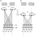
시차 배리어 방식을 사용한 3차원 표시에서의, 화소에 대한 관찰자의 안구 위치 및 관찰자와 화소 사이에 설치된 시차 배리어의 형태에 관해서, 도 10a를 사용하여 설명한다. 도 10a는 관찰자의 시점과, 관찰자의 좌우 안구를 통한 평면에 절단된 표시 패널(700)과, 시차 배리어(690)의 단면을 모식적으로 도시한다. 시차 배리어는 투광성 영역과 차광성 영역이 번갈아 설치되어 있고, 시차 배리어의 형태로서는 주로 스트라이프 형상의 형태가 사용된다. 또한, 도 10a에는 스트라이프 형상의 시차 배리어를 횡단하는 단면을 도시한다. 표시 패널(700)에는, 왼쪽 눈(10L)용의 제 1 화소 영역(710)과 오른쪽 눈(10R)용의 제 2 화소 영역(720)이 설치되고, 제 1 화소 영역(710)과 오른쪽 눈(10R) 사이 및 제 2 화소 영역(720)과 왼쪽 눈(10L) 사이에는 시차 배리어(690)가 형성되어 있다. 이와 같은 위치 관계에 있어서, 시차 배리어(690)는 좌우 각각의 눈에 안대로서 작용하게 된다. 그 결과, 관찰자는, 왼쪽 눈(10L)으로 왼쪽 눈용의 표시가 된 제 1 화소 영역(710)을, 오른쪽 눈(10R)으로 오른쪽 눈용의 표시가 된 제 2 화소 영역(720)을 보고, 3차원 표시를 눈으로 확인(視認)한다. 또한, 관찰자(10)가 오른쪽 눈(10R)으로 확인한 상(像)을 오른쪽 눈(10R) 위에, 왼쪽 눈(10L)으로 확인한 상을 왼쪽 눈(10L) 위에 나타낸다.In the three-dimensional display using the parallax barrier method, the eyeball position of the observer with respect to the pixel and the form of the parallax barrier provided between the observer and the pixel will be described with reference to FIG. 10A. FIG. 10A schematically illustrates a cross section of the observer's viewpoint, the
다음에, 관찰자가 표시 패널에 가까운 경우에 관해서, 도 10b를 사용하여 설명한다. 관찰자가 표시 패널에 가까우면, 왼쪽 눈(10L)으로 제 1 화소 영역(710)에 인접한 제 2 화소 영역(720)의 일부가 보이고, 오른쪽 눈(10R)으로 제 2 화소 영역(720)에 인접한 제 1 화소 영역(710)의 일부가 보이게 된다. 그 결과, 관찰자는, 왼쪽 눈(10L)으로는 보이지 않아야 할 오른쪽 눈(10R)용의 표시 중 일부를, 또한 오른쪽 눈(10R)으로는 보이지 않아야 할 왼쪽 눈(10L)용의 표시 중 일부를 보게 되어, 3차원 표시를 눈으로 확인하는 것이 곤란하게 된다. 또한, 관찰자(10)가 오른쪽 눈(10R)으로 확인한 상을 오른쪽 눈(10R) 위에, 왼쪽 눈(10L)으로 확인한 상을 왼쪽 눈(10L) 위에 나타낸다. 또한, 이와 같이 관찰자의 한쪽 눈에서는 보이지 않아야 할 다른 쪽 눈용의 표시 중 일부를, 한쪽 눈으로 보게 되는 것을 본 명세서에 있어서 크로스토크(crosstalk)라 한다.Next, the case where the observer is close to the display panel will be described with reference to FIG. 10B. When the observer is close to the display panel, the
<3차원 표시 장치를 따라서 관찰자가 이동하는 경우에 생기는 문제><Problem when the observer moves along the 3D display device>
다음에, 표시 패널의 주변부와 겹치는 시차 배리어의 형태와 중앙부와 겹치는 시차 배리어의 형태 차이를, 도 11을 사용하여 설명한다. 표시 패널(700)은, 관찰자(10)가 그의 중앙부(편의적으로 도면 중에 화살표를 사용하여 도시한다)와 마주하여 사용하는 3차원 표시 장치이다. 그의 중앙부에서는, 시차 배리어의 중심이 인접한 오른쪽 눈용 화소와 왼쪽 눈용 화소의 경계와 일치하도록 형성되어 있다. 도 11a에 도시한 표시 패널(700)의 중앙부에는, 제 1 화소 영역(710)에 포함되는 왼쪽 눈(10L)용의 화소와, 제 2 화소 영역(720)에 포함되는 오른쪽 눈(10R)용의 화소가 도시되어 있다. 한 세트의 오른쪽 눈용 화소와 왼쪽 눈용 화소를 아랫변으로 하고, 그 시차 배리어의 차광부를 윗변으로 하는 사다리꼴에 주목하면, 표시 패널(700)의 중앙부에 있어서, 그 사다리꼴(도면 중에 진한 해칭을 사용하여 도시한다)은 좌우로 균등하다. Next, the difference between the shape of the parallax barrier overlapping the periphery of the display panel and the parallax barrier overlapping the center is explained using FIG. 11. The
한편, 표시 패널(700)의 중앙부로부터 주변부를 향하여 멀어짐에 따라, 시차 배리어는 제 1 화소 영역(710)과 제 2 화소 영역(720)이 서로 접하는 경계의 바로 위보다 관찰자측(패널의 중앙부측이라고도 할 수 있다)에 형성된다. 왜냐하면, 관찰자는 표시 패널을 비스듬히 들여다 보는 위치에 서있기 때문에, 시차 배리어의 중심에 인접한 오른쪽 눈용 화소와 왼쪽 눈용 화소의 경계에 일치하여 형성하면, 관찰자는, 왼쪽 눈(10L)으로는 보이지 않아야 할 오른쪽 눈(10R)용의 표시 중 일부를, 또한 오른쪽 눈(10R)으로는 보이지 않아야 할 왼쪽 눈(10L)용의 표시 중 일부를 보게 되어, 3차원 표시를 눈으로 확인하는 것이 곤란하게 되기 때문이다. 따라서, 한 세트의 오른쪽 눈용 화소와 왼쪽 눈용 화소를 아랫변으로 하고, 그 시차 배리어의 차광부를 윗변으로 하는 사다리꼴에 주목하면, 표시 패널(700)의 중앙부로부터 주변부를 향하여 멀어짐에 따라, 그 사다리꼴은 표시 패널(700)의 중앙부측으로 기울어져 왜곡되도록, 시차 배리어를 설치한다. On the other hand, as the distance from the center of the
이와 같은 구성을 구비한 3차원 표시 장치에 있어서, 관찰자(10)가 그 중앙부로부터 표시 패널을 따라서 이동한 경우에 관해서, 도 11b를 사용하여 설명한다. 지면을 향하여 우측으로 이동한 관찰자(10)의 정면에, 한 세트의 오른쪽 눈용 화소와 왼쪽 눈용 화소를 아랫변으로 하고, 그 시차 배리어의 차광부를 윗변으로 하는 사다리꼴에 주목하면, 그 사다리꼴은 표시 패널(700)의 중앙부측으로 기울어져 왜곡된다. 그 결과, 관찰자는 왼쪽 눈(10L)으로는 보이지 않아야 할 오른쪽 눈(10R)용의 표시 중 일부를, 또한 오른쪽 눈(10R)으로는 보이지 않아야 할 왼쪽 눈(10L)용의 표시 중 일부를 보게 되어, 3차원 표시를 눈으로 확인하는 것이 곤란하게 된다. 이상의 사실로부터, 시차 배리어 방식으로 3차원 표시를 행하기 위해서는, 표시 화면과 관찰차의 눈이 특정한 위치 관계에 있을 필요가 있다. In the three-dimensional display device having such a configuration, the case where the
본 발명의 일 형태는, 이와 같은 기술적 배경하에 이루어진 것이다. 따라서, 본 발명의 일 형태는, 특정한 관찰자가 나안으로 3차원 표시를 눈으로 확인할 수 있는 범위가 확대된 표시 장치를 제공하는 것을 과제 중 하나로 한다. 또는, 본 발명의 일 형태는, 특정한 관찰자가 나안으로 3차원 표시를 눈으로 확인할 수 있는 범위를 확대한 표시 장치의 구동 방법을 제공하는 것을 과제 중 하나로 한다.One embodiment of the present invention is made under such a technical background. Accordingly, one aspect of the present invention is to provide a display device in which a specific observer can visually check a three-dimensional display with naked eyes. Another object of one embodiment of the present invention is to provide a method of driving a display device in which a specific observer enlarges the range in which a three-dimensional display can be visually checked with the naked eye.
상기 과제를 해결하기 위하여, 본 발명의 일 형태는, 표시 장치에 설치된 화소에 대한 관찰자의 위치 및 상기 관찰자와 상기 화소 사이에 설치하는 시차 배리어의 형태에 착안하였다. 그래서, 본 명세서에 예시된 구성을 구비한 표시 장치에 도달하였다. 본 발명의 일 형태는, 화소에 대한 관찰자의 위치를, 초음파를 사용하여 특정하고, 그 위치에 따라 시차 배리어의 형태를 변화시킨 구성을 구비한다. In order to solve the said subject, one aspect of this invention paid attention to the position of the observer with respect to the pixel provided in the display apparatus, and the form of the parallax barrier provided between the said observer and the said pixel. Thus, a display device having the configuration illustrated in the present specification has been reached. One embodiment of the present invention has a configuration in which the position of an observer with respect to a pixel is specified using ultrasonic waves, and the form of the parallax barrier is changed in accordance with the position.
즉, 본 발명의 일 형태는, 왼쪽 눈용의 제 1 화소 영역과 오른쪽 눈용의 제 2 화소 영역을 구비한 표시 패널과, 표시 패널의 일부를 차단하고, 형태가 가변적인 시차 배리어와, 시차 배리어의 형태를 제어하는 시차 배리어 제어 회로와, 복수의 검지기와, 초음파 발진기를 갖고, 복수의 검지기가 특정한 관찰자의 위치에 따라서, 시차 배리어가 시차 배리어 제어 회로에 의해, 관찰자의 오른쪽 눈으로부터 제 1 화소 영역을 차단하고, 또한 관찰자의 왼쪽 눈으로부터 제 2 화소 영역을 차단하도록 구성되어 있는 표시 장치이다. That is, one embodiment of the present invention provides a display panel having a first pixel region for the left eye and a second pixel region for the right eye, a parallax barrier having a variable shape by blocking a part of the display panel, and a parallax barrier. The parallax barrier has a parallax barrier control circuit for controlling the shape, a plurality of detectors and an ultrasonic oscillator, and the plurality of detectors are arranged by the parallax barrier control circuit according to the position of a specific observer, so that the first pixel region is separated from the observer's right eye. And a second pixel area from the observer's left eye.
상기 본 발명의 일 형태의 표시 장치는, 복수의 검지기와 초음파 발진기를 사용하여 특정한 관찰자의 화소에 대한 위치에 따라서, 시차 배리어의 형태를 변화시킨 구성을 갖는다. 이에 따라, 특정한 관찰자의 오른쪽 눈과 왼쪽 눈의, 표시 장치가 구비한 각 화소에 대한 위치를 알 수 있다. 그 결과, 특정한 관찰자가 나안으로 3차원 표시를 눈으로 확인할 수 있는 범위가 확대된 표시 장치를 제공할 수 있다. 또한, 초음파를 사용하기 때문에, 어두운 환경에서도, 관찰자의 위치를 정확하게 검지할 수 있다. 그 결과, 관찰자는 보다 밝고 선명한 3차원 표시 화상을 눈으로 확인할 수 있다.The display device of one embodiment of the present invention has a configuration in which the shape of the parallax barrier is changed in accordance with a position of a specific observer's pixel using a plurality of detectors and an ultrasonic oscillator. Accordingly, the position of each pixel included in the display device of the right eye and the left eye of a particular observer can be known. As a result, it is possible to provide a display device having an enlarged range in which a specific observer can visually check a three-dimensional display with naked eyes. In addition, since ultrasonic waves are used, the position of the observer can be detected accurately even in a dark environment. As a result, an observer can visually confirm a brighter and clearer three-dimensional display image.
또한, 본 발명의 일 형태는, 시차 배리어가 한 쌍의 기판들에 협지(挾持)된 액정층을 사용하여 형성되고, 한 쌍의 기판 중 적어도 한쪽은 액정층의 배향을 제어하는 복수의 전극을 구비하고, 복수의 전극 각각이 시차 배리어 제어 회로와 전기적으로 접속되는 상기한 표시 장치이다. Moreover, one form of this invention is formed using the liquid crystal layer by which the parallax barrier was pinched by a pair of board | substrate, At least one of a pair of board | substrate provides a some electrode which controls the orientation of a liquid crystal layer. And a plurality of electrodes, each of which is electrically connected to a parallax barrier control circuit.
상기 본 발명의 일 형태의 표시 장치는, 시차 배리어가, 액정층과 상기 액정층의 배향을 제어하는 전극이 복수 설치되고, 상기 전극 각각이 시차 배리어 제어 회로와 전기적으로 접속된다. 이에 따라, 특정한 관찰자의 위치에 따라서, 시차 배리어가 상기 관찰자의 오른쪽 눈으로부터 제 1 화소 영역을 차단하고, 또한 상기 관찰자의 왼쪽 눈으로부터 제 2 화소 영역을 차단하도록, 시차 배리어 제어 회로를 사용하여, 시차 배리어의 형태를 변화시킬 수 있다. 그 결과, 특정한 관찰자가 나안으로 3차원 표시를 눈으로 확인할 수 있는 범위가 확대된 표시 장치를 제공할 수 있다. In the display device of one embodiment of the present invention, a parallax barrier is provided with a plurality of electrodes for controlling the alignment of the liquid crystal layer and the liquid crystal layer, and each of the electrodes is electrically connected to a parallax barrier control circuit. Thus, according to the position of a particular observer, using a parallax barrier control circuit such that the parallax barrier blocks the first pixel region from the right eye of the observer and also blocks the second pixel region from the left eye of the observer, The shape of the parallax barrier can be changed. As a result, it is possible to provide a display device having an enlarged range in which a specific observer can visually check a three-dimensional display with naked eyes.
또한, 본 발명의 일 형태는, 표시 장치의 표시면이 관찰자와 마주하는 측에 펄스형 초음파를 발신하는 제 1 단계와, 펄스형의 초음파 반사파가 복수의 검지기 각각에 도달할 때까지의 시간을 이용하여, 관찰자의 유무 및 위치를 특정하는 제 2 단계를 갖는다. 또한, 관찰자의 위치를 지나는 직선이 표시면과 수직으로 교차하는 좌표를 산출하여, 관찰자의 정면과 마주하는 한 쌍의 오른쪽 눈용의 화소와 왼쪽 눈용의 화소를 특정하는 제 3 단계와, 상기 한 쌍의 오른쪽 눈용의 화소와 왼쪽 눈용의 화소로부터 상기 관찰자까지의 거리를 특정하는 제 4 단계를 갖는다. 또한, 관찰자의 오른쪽 눈이 상기 오른쪽 눈용의 화소를, 관찰자의 왼쪽 눈이 상기 왼쪽 눈용의 화소를 관찰할 수 있도록, 상기 한 쌍의 오른쪽 눈용의 화소와 왼쪽 눈용의 화소에 대응하는 시차 배리어의 크기를, 관찰자까지의 거리를 이용하여 제어하는 제 5 단계를 갖는다. 또한, 다른 한 쌍의 오른쪽 눈용 화소와 왼쪽 눈용의 화소를 아랫변으로 하고, 그 시차 배리어의 차광부를 윗변으로 하는 사다리꼴이, 관찰자의 정면과 마주하는 화소로부터 좌우 방향으로 멀어질수록 관찰자측으로 기울어져 왜곡되고, 관찰자의 왼쪽 눈으로부터 오른쪽 눈용의 화소 영역을 차단하고, 또한 관찰자의 오른쪽 눈으로부터 왼쪽 눈용의 화소 영역을 차단하도록 시차 배리어를 형성하는 제 6 단계를 갖는 표시 장치의 구동 방법이다. In addition, one embodiment of the present invention provides a first step of transmitting pulsed ultrasonic waves to a side where a display surface of a display device faces an observer, and a time until a pulsed ultrasonic reflected wave reaches each of a plurality of detectors. The second step is to specify the presence and location of the observer. And a third step of calculating coordinates at which a straight line passing through the observer's position intersects the display surface perpendicularly, specifying a pair of right eye pixels and left eye pixels facing the front of the observer; And a fourth step of specifying a distance from the right eye pixel and the left eye pixel to the viewer. The size of the parallax barrier corresponding to the pair of right eye pixels and the left eye pixels so that the observer's right eye can observe the right eye pixel and the observer's left eye can observe the pixel for the left eye. It has a fifth step of controlling using the distance to the observer. In addition, the trapezoid having the other pair of right eye pixels and left eye pixels as the lower side and the light shielding portion of the parallax barrier as the upper side is inclined toward the observer side as it moves away from the pixel facing the front of the observer in the left and right direction. A driving method of a display device having a sixth step of distorting and blocking a pixel region for a right eye from a viewer's left eye and further blocking a pixel region for a left eye from a viewer's right eye.
상기 본 발명의 일 형태의 표시 장치의 구동 방법에 의하면, 특정한 관찰자의 위치에 따라서, 시차 배리어가 상기 관찰자의 오른쪽 눈으로부터 제 1 화소 영역을 차단하고, 또한 상기 관찰자의 왼쪽 눈으로부터 제 2 화소 영역을 차단하도록, 시차 배리어 제어 회로를 사용하여, 시차 배리어의 형태를 변화시킬 수 있다. 그 결과, 특정한 관찰자가 나안으로 3차원 표시를 눈으로 확인할 수 있는 범위가 확대된 표시 장치의 구동 방법을 제공할 수 있다.According to the driving method of the display device of one embodiment of the present invention, the parallax barrier blocks the first pixel region from the right eye of the observer and the second pixel region from the left eye of the observer according to the position of a specific observer. The parallax barrier control circuit can be used to change the shape of the parallax barrier so as to block. As a result, it is possible to provide a method of driving a display device in which a range where a particular observer can visually check a three-dimensional display with naked eyes.
본 발명의 일 형태에 의하면, 특정한 관찰자가 나안으로 3차원 표시를 눈으로 확인할 수 있는 범위가 확대된 표시 장치를 제공할 수 있다. 또한, 본 발명의 일 형태는, 특정한 관찰자가 나안으로 3차원 표시를 눈으로 확인할 수 있는 범위를 확대한 표시 장치의 구동 방법을 제공할 수 있다. According to one embodiment of the present invention, it is possible to provide a display device having an enlarged range in which a specific observer can visually check a three-dimensional display with naked eyes. In addition, one embodiment of the present invention can provide a method for driving a display device in which a specific observer enlarges the range in which a three-dimensional display can be visually checked with the naked eye.
도 1a 및 도 1b는 실시형태에 따른 표시 장치와 사용자의 위치 및 표시 장치의 구성을 설명하는 도면.
도 2a 및 도 2b는 실시형태에 따른 표시 패널과 관찰자의 거리와 시차 배리어의 형태 관계를 설명하는 도면.
도 3a 및 도 3b는 실시형태에 따른 표시 패널을 따라서 이동하는 관찰자의 위치와 시차 배리어의 형태 관계를 설명하는 도면.
도 4a1 내지 도 4b2는 실시형태에 따른 시차 배리어를 설명하는 도면.
도 5는 실시형태에 따른 시차 배리어를 설명하는 도면.
도 6a 및 도 6b는 실시형태에 따른 표시 패널을 설명하는 도면.
도 7a 및 도 7b는 실시형태에 따른 표시 패널을 설명하는 도면.
도 8a 및 도 8b는 실시형태에 따른 터치 패널을 구비하는 셔터 패널을 설명하는 도면.
도 9a 내지 도 9c는 실시형태에 따른 전자 기기를 설명하는 도면.
도 10a 및 도 10b는 종래 기술을 설명하는 도면.
도 11a 및 도 11b는 종래 기술을 설명하는 도면.
도 12는 실시예에 따른 3차원 표시 장치를 설명하는 블록도.
도 13a-L, 13a-R, 및 도 13b는 실시예에 따른 3차원 표시 장치의 평가 방법을 설명하는 도면.
도 14는 실시예에 따른 3차원 표시 장치의 평가 결과를 설명하는 도면.
도 15는 비교예에 따른 3차원 표시 장치의 평가 결과를 설명하는 도면.
도 16은 트랜지스터의 특성을 설명하는 도면.
도 17a 내지 도 17d는 초음파 센서를 설명하는 도면. 1A and 1B illustrate a display device according to an embodiment, a position of a user, and a configuration of the display device.
2A and 2B illustrate a form relationship between a distance between a display panel and an observer and a parallax barrier according to an embodiment;
3A and 3B illustrate a form relationship between a position of an observer moving along a display panel according to an embodiment and a parallax barrier.
4A1 to 4B2 illustrate a parallax barrier according to an embodiment.
5 is a diagram illustrating a parallax barrier according to an embodiment.
6A and 6B illustrate a display panel according to an embodiment.
7A and 7B illustrate a display panel according to an embodiment.
8A and 8B illustrate a shutter panel including a touch panel according to an embodiment.
9A to 9C are diagrams illustrating an electronic device according to an embodiment.
10A and 10B illustrate the prior art;
11A and 11B illustrate a prior art.
12 is a block diagram illustrating a three-dimensional display device according to an embodiment.
13A-L, 13A-R, and 13B illustrate an evaluation method of a three-dimensional display device according to an embodiment.
14 is a diagram illustrating an evaluation result of a three-dimensional display device according to an embodiment.
15 is a diagram illustrating an evaluation result of a three-dimensional display device according to a comparative example.
16 is a diagram illustrating the characteristics of a transistor.
17A to 17D are diagrams for explaining an ultrasonic sensor.
실시형태에 관해서, 도면을 사용하여 상세하게 설명한다. 단, 본 발명은 이하의 설명에 한정되지 않고, 본 발명의 취지 및 그 범위에서 일탈하지 않고 그 형태 및 상세한 설명을 다양하게 변경할 수 있는 것은 당업자라면 용이하게 이해한다. 따라서, 본 발명은 이하에 나타내는 실시형태의 기재 내용에 한정하여 해석되는 것은 아니다. 또한, 이하에 설명하는 발명의 구성에 있어서, 동일 부분 또는 동일한 기능을 갖는 부분에는 동일 부호를 다른 도면 사이에서 공통으로 사용하고, 그 반복 설명은 생략한다.EMBODIMENT OF THE INVENTION Embodiment is described in detail using drawing. However, the present invention is not limited to the following description, and it is easily understood by those skilled in the art that the form and detailed description can be variously changed without departing from the spirit and scope of the present invention. Therefore, the present invention is not construed as being limited to the description of the embodiments described below. In addition, in the structure of the invention demonstrated below, the same code | symbol is used in common among the other parts in the same part or the part which has the same function, and the repeated description is abbreviate | omitted.
(실시형태 1)(Embodiment 1)
본 실시형태에서는, 화소에 대한 관찰자의 위치를, 초음파를 사용하여 특정하고, 그 위치에 따라서 시차 배리어의 형태를 변화시킨 구성을 구비하는 표시 장치에 관해서 도 1a 내지 도 3b를 참조하여 설명한다. 구체적으로는, 제 1 화소 영역과 제 2 화소 영역을 구비하는 표시 패널과, 표시 패널의 일부를 차단하고, 형태가 가변적인 시차 배리어와, 시차 배리어의 형태를 제어하는 시차 배리어 제어 회로와, 복수의 검지기와, 초음파 발진기를 갖고, 복수의 검지기가 특정한 관찰자의 위치에 따라서, 시차 배리어가 시차 배리어 제어 회로에 의해, 관찰자의 오른쪽 눈으로부터 제 1 화소 영역을 차단하고, 또한 상기 관찰자의 왼쪽 눈으로부터 제 2 화소 영역을 차단하도록 구성되어 있는 표시 장치에 관해서 설명한다. In this embodiment, a display device having a configuration in which the position of an observer with respect to a pixel is specified using ultrasonic waves and the parallax barrier is changed in accordance with the position will be described with reference to FIGS. 1A to 3B. Specifically, a display panel having a first pixel region and a second pixel region, a parallax barrier that blocks a portion of the display panel, and whose shape is variable, a parallax barrier control circuit that controls the form of the parallax barrier, and a plurality of And a plurality of detectors according to the position of a particular observer, the parallax barrier blocks the first pixel region from the right eye of the observer by means of a parallax barrier control circuit, and from the left eye of the observer A display device configured to block the second pixel region will be described.
<표시 장치의 구성><Configuration of Display Device>
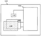
본 발명의 일 형태의 표시 장치(20)와, 이것을 사용하는 관찰자(10)의 위치를 도 1a에 도시한다. 관찰자(10)는 표시면과 마주하여 표시 장치(20)를 사용한다. The position of the
표시 장치(20)는, 표시 패널(200)과, 표시 패널(200)의 표시면측에 시차 배리어를 형성하는 셔터 패널(100)과, 제어 장치(30)를 구비한다. 또한, 초음파 발진기(161)와 복수의 검지기(162R) 및 검지기(162L)를 구비하고, 초음파 발진기(161)가 관찰자(10)를 향하여 발하는 초음파의 반사파를 상기 검지기가 수신하도록 배치되어 있다. The
제어 장치(30)의 상세를 도 1b에 도시한 블록도를 참조하여 설명한다. 제어 장치(30)는, 관찰자 검지 회로(160)와, 화상 신호 생성 회로(260)와, 시차 배리어 제어 회로(150)와, 표시 패널 구동 회로(250)를 구비한다. 화상 신호 생성 회로(260)는 표시 패널(200)과 표시 패널 구동 회로(250)를 통하여 전기적으로 접속되고, 셔터 패널(100)과 시차 배리어 제어 회로(150)를 통하여 전기적으로 접속되어 있다. 또한, 초음파 발진기(161)와, 복수의 검지기(162R) 및 검지기(162L)는 관찰자 검지 회로(160)와 접속되고, 관찰자 검지 회로(160)는 시차 배리어 제어 회로(150) 및 화상 신호 생성 회로(260)와 전기적으로 접속되어 있다. The detail of the
화상 신호 생성 회로(260)는, 기억 매체에 기록된 화상 데이터나 접속된 외부 기기로부터 입력되는 화상 데이터를, 본 실시형태에서 예시하는 표시 장치로 표시 가능한 화상 신호로 변환하여 출력한다. 또한, 예를 들어 관찰자 검지 회로(160)가 출력하는 관찰자의 위치를 특정한 신호에 따라서, 화상 신호를 변환하는 작용을 한다. 구체적으로는, 표시 패널(200)과 마주하는 관찰자의 위치로부터 관찰자의 양쪽 눈의 위치를 추측하고, 관찰자가 3차원 화상을 눈으로 확인하기 용이하도록 시차 배리어의 형태를 결정하고, 시차 배리어 제어 회로(150)에, 결정된 시차 배리어의 형태가 되도록 시차 배리어 제어 신호를 출력한다. The image
또한, 화상 신호 생성 회로(260)는 관찰자의 위치 정보 등에 따라서, 게임 기기로부터 출력되는 화상 신호를 바꿀 수도 있다. 예를 들어 게임에서 검지한 관찰자의 자세에 따라서 복수의 선택 사항으로부터 다음의 전개를 결정하여도 좋다. The image
시차 배리어 제어 회로(150)는, 화상 신호 생성 회로(260)가 출력하는 시차 배리어 제어 신호에 따라서 셔터 패널(100)을 구동하고, 시차 배리어의 형태를 변화시킨다. The parallax
표시 패널 구동 회로(250)는, 화상 신호 생성 회로(260)가 출력하는 화상 신호에 따라서 표시 패널(200)을 구동하고, 화상을 표시하는 회로이다. The display
<표시 장치의 구동 방법><Drive method of the display device>
본 발명의 일 형태의 표시 장치(20)의 구동 방법에 관해서 설명한다. 표시 장치(20)는 이하의 6개 단계를 반복하면서 동작한다. A driving method of the
제 1 단계에 있어서는, 초음파 발진기(161)가 펄스형 초음파를 표시면측으로 발신하고, 제 2 단계에 있어서는, 펄스형 초음파의 반사파가 복수의 검지기 각각에 도달할 때까지의 시간을 이용하여, 관찰자의 유무 및 위치를 특정한다. In the first step, the
계속되는 제 3 단계에 있어서는, 화상 신호 생성 회로(260)가 관찰자의 위치를 지나는 직선이 표시면에 수직으로 교차하는 좌표를 산출하여, 관찰자의 정면과 마주하는 한 쌍의 오른쪽 눈용의 화소와 왼쪽 눈용의 화소를 특정한다. 또한, 제 4 단계에 있어서는, 화상 신호 생성 회로(260)가 한 쌍의 오른쪽 눈용의 화소와 왼쪽 눈용의 화소로부터 관찰자까지의 거리를 특정한다. In the subsequent third step, the image
다음에, 제 5 단계에 있어서는, 화상 신호 생성 회로(260)가 시차 배리어 제어 회로(150)를 통하여, 관찰자의 오른쪽 눈이 오른쪽 눈용의 화소를, 관찰자의 왼쪽 눈이 왼쪽 눈용의 화소를 관찰할 수 있도록, 한 쌍의 오른쪽 눈용의 화소와 왼쪽 눈용의 화소에 대응하는 시차 배리어의 크기를, 관찰자까지의 거리를 이용하여 제어한다. Next, in the fifth step, the image
제 6 단계에 있어서는, 화상 신호 생성 회로(260)가 시차 배리어 제어 회로(150)를 통하여, 다른 한 쌍의 오른쪽 눈용 화소와 왼쪽 눈용의 화소를 아랫변으로 하고, 그 시차 배리어의 차광부를 윗변으로 하는 사다리꼴이, 관찰자의 정면과 마주하는 화소로부터 좌우 방향으로 멀어질수록, 관찰자측으로 기울어져 왜곡되고, 관찰자의 왼쪽 눈으로부터 오른쪽 눈용의 화소 영역을 차단하고, 또한 관찰자의 오른쪽 눈으로부터 왼쪽 눈용의 화소 영역을 차단하도록 시차 배리어를 형성한다. 또한, 제 6 단계는 제 5 단계와 동시에 행하여도 좋다. In the sixth step, the image
<화소에 대한 관찰자의 위치를 특정하는 방법><Method of specifying position of observer with respect to pixel>
본 실시형태에서는, 2개의 검지기(162R)와 검지기(162L) 사이에 설치된 초음파 발진기(161)에 접속된 관찰자 검지 회로(160)에 의해, 관찰자의 위치를 특정한다. 구체적으로는, 초음파 발진기(161)를 사용하여, 표시 장치의 표시면과 마주하는 공간에 펄스형의 초음파를 발신한다. 상기 공간에 관찰자가 있으면, 상기 펄스형의 초음파를 반사하고, 반사파는 검지기(162R)와 검지기(162L)로 검지된다. 그러나, 상기 공간에 관찰자가 없으면, 상기 펄스형의 초음파는 반사파를 반환하지 않고 상기 공간을 통과한다. In the present embodiment, the position of the observer is specified by the
관찰자 검지 회로(160)는, 초음파 발진기(161)를 사용하여 펄스형의 초음파를 발한 때부터, 반사파가 검지기(162R) 및 검지기(162L)에 검지될 때까지의 시간을 계측하고, 상기 공간에 물체가 있는지 없는지를 검지한다. 또한, 상기 공간에 물체가 있는 경우에는, 물체와 검지기(162R)의 거리 및 물체와 검지기(162L)의 거리를 각각 알 수 있다. 또한, 반사파의 강도를 사용하여 물체의 위치 정보를 얻을 수도 있다.The
또한, 검지기(162R) 및 검지기(162L)는 표시 패널에 대하여 특정한 위치에 고정되어 있다. 예를 들어, 도 1a에 도시한 바와 같이, 검지기(162R)를 표시 패널의 우측 단부에, 검지기(162L)를 좌측 단부에 고정한다. 또한, 화소도 패널의 특정한 위치에 고정되어 있다. 따라서, 표시 패널에 대하여 특정한 위치에 고정된 복수의 검지기를 사용하여, 관찰자의 위치를 검지함으로써, 화소에 대한 관측자의 위치를 특정할 수 있다. In addition, the
또한, 초음파 발진기의 수도 1개 이상이면 좋고, 복수의 발진기를 사용할 수 있다. 또한, 검지기는 여러 번 사용하면 좋고, 그 수는 2개로 한정되지 않는다. 서로 떨어져 설치된 검지기의 수를 늘리면, 관찰자의 위치를 특정하는 정밀도를 높일 수 있다. 초음파 발진기를 설치하는 위치는, 초음파 발진기가 발한 초음파를 관찰자가 반사하고, 그 반사파를 검지기가 수신한 구성이면, 검지기 사이로 한정되지 않는다. In addition, the number of ultrasonic oscillators may be one or more, and a plurality of oscillators may be used. In addition, you may use a probe several times, and the number is not limited to two. Increasing the number of detectors provided apart from each other can increase the accuracy of specifying the position of the observer. The position at which the ultrasonic oscillator is provided is not limited between the detectors as long as the observer reflects the ultrasonic wave emitted by the ultrasonic oscillator and the detector receives the reflected wave.
<관찰자의 위치에 따른 시차 배리어의 형태><Type of parallax barrier according to observer's position>
다음에, 관찰자 검지 회로(160)가 특정한 관찰자의 위치에 따른 시차 배리어의 형태에 관해서 설명한다. Next, the form of the parallax barrier according to the position of the specific observer by the
시차 배리어의 형태와, 관찰자와 표시 패널 사이의 거리 관계를 도 2a 및 도 2b에 모식적으로 도시한다. 도 2a는 관찰자의 시점과, 관찰자의 좌우 안구를 지나는 평면으로 절단된 표시 패널(200)과, 시차 배리어(90)의 단면을 모식적으로 도시하고 있다. 시차 배리어는 투광성 영역과 차광성 영역이 번갈아 설치되어 있고, 시차 배리어의 형태로서는 스트라이프 형상, 체크무늬 형상, 십자 형상(crossed pattern) 등을 사용할 수 있다. 또한, 도 2a에는, 스트라이프 형상의 시차 배리어를 횡단하는 단면을 도시하고 있다. 관찰자(10)가 표시 패널(200)에 가까우면, 시차 배리어의 간극으로부터 보이는 표시 패널의 범위가 넓어진다. 구체적으로는, 왼쪽 눈에서 제 1 화소 영역에 인접하는 제 2 화소 영역의 일부가 보이고, 오른쪽 눈에서 제 2 화소 영역에 인접하는 제 1 화소 영역의 일부가 보이게 된다. 그 결과, 관찰자는, 왼쪽 눈에서는 보이지 않아야 할 오른쪽 눈용의 표시 중 일부를, 또한 오른쪽 눈에서는 보이지 않아야 할 왼쪽 눈용의 표시 중 일부를 보게 되어, 3차원 표시를 눈으로 확인하는 것이 곤란하게 된다. The shape of the parallax barrier and the distance relationship between the observer and the display panel are schematically illustrated in FIGS. 2A and 2B. FIG. 2A schematically illustrates a cross section of the
여기서, 본 발명의 일 형태는 관찰자의 위치에 따라서, 시차 배리어의 형태를 변화시키는 것이다. 구체적으로는 스트라이프 형상의 시차 배리어의 차광부 폭을 넓혀서, 그 간격을 좁히는 구성으로 한다. 예를 들어, 도 2b에 도시한 바와 같이, 시차 배리어(90)는, 도 2a에 비하여 표시 패널(200)에 가까운 관찰자(10)에 맞추어 차광부의 폭을 크게 하고, 투광부의 폭을 좁힌다. 이와 같은 구성에 의해 시차 배리어의 형태를 제어함으로써, 관찰자가 표시 패널에 가까워도, 왼쪽 눈은 제 1 화소 영역만을, 오른쪽 눈은 제 2 화소 영역만을 관찰할 수 있도록 된다. In one embodiment of the present invention, the form of the parallax barrier is changed in accordance with the position of the observer. Specifically, the width of the light shielding portion of the stripe parallax barrier is increased to narrow the gap. For example, as shown in FIG. 2B, the
다음에, 관찰자(10)가 중앙부로부터 표시 패널을 따라서 이동하는 경우에 관해서, 한 세트의 오른쪽 눈용 화소와 왼쪽 눈용의 화소를 아랫변으로 하고, 그 시차 배리어의 차광부를 윗변으로 하는 사다리꼴에 주목하여 도 3a 및 도 3b를 사용하여 설명한다. Next, with respect to the case where the
표시 패널의 중앙부에 관찰자(10)가 마주한 상태에서 최적화된 시차 배리어(90)의 형태에 있어서(도 3a 참조), 그 사다리꼴은 표시 패널(200)의 중앙부측으로 기울어져 왜곡되고 있기 때문에, 관찰자가 표시 패널을 따라서 이동하면 3차원 표시를 눈으로 확인하는 것이 곤란하게 된다. In the form of the
따라서, 본 발명의 일 형태는 관찰자의 위치에 따라서, 시차 배리어의 형태를 변화시키는 것이다. 구체적으로는 관찰자의 정면에서, 시차 배리어(예를 들어, 스트라이프 형상의 차광부)의 중심이 인접하는 오른쪽 눈용 화소와 왼쪽 눈용 화소의 경계와 일치하도록 형성한다. 예를 들어, 도 3b에 도시한 바와 같이, 왼쪽 눈(10L)용의 제 1 화소 영역(210)에 포함되는 왼쪽 눈용의 화소와, 오른쪽 눈(10R)용의 제 2 화소 영역(220)에 포함되는 오른쪽 눈용의 화소를 아랫변으로 하고,그 시차 배리어(90)의 차광부를 윗변으로 하는 사다리꼴은, 관찰자(10)의 정면에서, 좌우로 균등하게 되도록 시차 배리어(90)를 형성한다. Therefore, one embodiment of the present invention changes the form of the parallax barrier in accordance with the position of the observer. Specifically, the front of the observer is formed such that the center of the parallax barrier (for example, the stripe-shaped light shielding portion) coincides with the boundary between the adjacent right eye pixel and the left eye pixel. For example, as shown in FIG. 3B, the pixel for the left eye included in the
이와 같은 구성으로 함으로써, 관찰자(10)의 정면에서, 왼쪽 눈은 제 1 화소 영역(210)만을, 오른쪽 눈은 제 2 화소 영역(220)만을 관찰할 수 있도록 된다. With such a configuration, the left eye can observe only the
또한, 관찰자의 우측 또는 좌측에 있는 시차 배리어는, 관찰자의 정면으로부터 멀어짐에 따라 그 사다리꼴이 관찰자의 정면측으로 기울어져 왜곡되어, 스트라이프 형상의 시차 배리어를 형성한다. 왜냐하면, 관찰자는 표시 패널을 비스듬히 들여다 보는 위치에 서있기 때문에, 시차 배리어의 중심이 한 쌍의 오른쪽 눈용 화소와 왼쪽 눈용 화소의 경계에 일치하여 형성되어 있으면, 왼쪽 눈에 오른쪽 눈용의 표시가, 오른쪽 눈에는 왼쪽 눈용의 표시가 보이기 때문이다. 따라서, 한 세트의 오른쪽 눈용 화소와 왼쪽 눈용의 화소를 아랫변으로 하고, 그 시차 배리어의 차광부를 윗변으로 하는 사다리꼴에 주목하면, 관찰자의 정면으로부터 멀어짐에 따라서, 그 사다리꼴은 관찰자의 정면측으로 기울어져 왜곡되도록 스트라이프 형상의 시차 배리어의 차광부 폭 및 간격을 제어하여 형성할 필요가 있다. Further, as the parallax barrier on the right or left side of the observer moves away from the front side of the observer, the trapezoid is inclined and distorted toward the front side of the observer, thereby forming a stripe parallax barrier. Because the observer stands at a position looking into the display panel at an angle, if the center of the parallax barrier is formed coincident with the boundary between a pair of right eye pixels and left eye pixels, a right eye indication is displayed in the left eye, and the right eye is right. This is because there is a mark for the left eye. Therefore, when paying attention to a trapezoid having a set of the right eye pixel and the left eye pixel as the lower side and the light shielding portion of the parallax barrier as the upper side, the trapezoid is inclined toward the front side of the observer as it moves away from the front of the observer. It is necessary to control and form the light shielding part width and the space | interval of a stripe parallax barrier so that it may be distorted.
이와 같은 구성으로 함으로써, 관찰자의 정면으로부터 벗어난 방향에 있어서, 왼쪽 눈은 제 1 화소 영역(210)만을, 오른쪽 눈은 제 2 화소 영역(220)만을 관찰할 수 있도록 된다. With such a configuration, the left eye can observe only the
상기 본 발명의 일 형태의 표시 장치는, 복수의 검지기와 초음파 발진기를 사용하여 특정한 관찰자의 화소에 대한 위치에 따라서, 시차 배리어의 형태를 변화시킨 구성을 갖는다. 이에 따라, 특정한 관찰자의 오른쪽 눈과 왼쪽 눈의, 표시 장치가 구비하는 각 화소에 대한 위치를 알 수 있다. 그 결과, 특정한 관찰자가 나안으로 3차원 표시를 눈으로 확인할 수 있는 범위가 확대된 표시 장치를 제공할 수 있다. 또한, 초음파를 사용하기 때문에, 어두운 환경에서도, 관찰자의 위치를 정확하게 검지할 수 있다. 그 결과, 관찰자는 보다 밝고 선명한 3차원 표시 화상을 눈으로 확인할 수 있다.The display device of one embodiment of the present invention has a configuration in which the shape of the parallax barrier is changed in accordance with a position of a specific observer's pixel using a plurality of detectors and an ultrasonic oscillator. Accordingly, the position of each pixel included in the display device of the right eye and the left eye of a particular observer can be known. As a result, it is possible to provide a display device having an enlarged range in which a specific observer can visually check a three-dimensional display with naked eyes. In addition, since ultrasonic waves are used, the position of the observer can be detected accurately even in a dark environment. As a result, an observer can visually confirm a brighter and clearer three-dimensional display image.
또한, 본 실시형태는 본 명세서에서 나타내는 다른 실시형태와 적절히 조합할 수 있다. In addition, this embodiment can be combined suitably with the other embodiment shown in this specification.
(실시형태 2)(Embodiment 2)
본 실시형태에서는, 화소에 대한 관찰자의 위치에 따라서 시차 배리어의 형태를 변화시킨 구성을 구비하는 표시 장치에 적용 가능한 셔터 패널에 관해서 도 4a1 내지 도 4b2 및 도 5를 참조하여 설명한다. 구체적으로는, 한 쌍의 기판에 협지된 액정층을 갖고, 한 쌍의 기판 중 적어도 한쪽은 상기 액정층의 배향을 제어하는 복수의 전극을 구비하고, 상기 복수 전극의 각각이 시차 배리어 제어 회로와 전기적으로 접속되는 셔터 패널의 구성에 관해서 설명한다. In this embodiment, a shutter panel applicable to a display device having a configuration in which the shape of the parallax barrier is changed in accordance with the position of the observer with respect to the pixel will be described with reference to FIGS. 4A1 to 4B2 and FIG. 5. Specifically, a liquid crystal layer sandwiched between a pair of substrates, at least one of the pair of substrates includes a plurality of electrodes for controlling the alignment of the liquid crystal layer, and each of the plurality of electrodes includes a differential barrier control circuit; The structure of the shutter panel electrically connected is demonstrated.
셔터 패널은 다양한 형태의 시차 배리어를 형성한다. 구체적으로는, 차광 또는 투광을 전환하는 복수의 광학 소자를 사용하여 셔터 패널이 구성된다. 차광 또는 투광을 전환하는 광학 소자로서는, 한 쌍의 전극 사이에 액정을 포함하는 액정 소자를 적합하게 사용할 수 있다. 액정 소자는, 한 쌍의 전극에 끼워진 액정층에 전계를 인가하여 액정의 배향을 제어하고, 차광 또는 투광을 선택적으로 제어할 수 있다. The shutter panel forms various types of parallax barriers. Specifically, the shutter panel is configured by using a plurality of optical elements that switch light shielding or light projection. As an optical element which switches light shielding or light projection, a liquid crystal element containing a liquid crystal can be suitably used between a pair of electrodes. The liquid crystal element can control the alignment of the liquid crystal by selectively applying an electric field to the liquid crystal layer sandwiched between the pair of electrodes, and selectively control the light shielding or the light transmission.
<셔터 패널의 구성><Configuration of the Shutter Panel>
셔터 패널(100)의 상면도를 도 4a1에, 도 4a1에서의 절단선(Y1-Y2)에 따른 단면도를 도 4a2에 도시한다. The top view of the
셔터 패널(100)은, 기판(101)에 전극(106)과, 기판(102)에 전극(105)을 구비한다. 전극(106)은 복수의 스트라이프 형상의 전극(106a1, 106a2, 106a3, 106b1, 106b2, 106b3, 106c1, 106c2 및 106c3)을 포함하고, 전극(105)은 복수의 스트라이프 형상의 전극(105a1, 105a2, 105a3, 105b1, 105b2, 105b3, 105c1, 105c2 및 105c3)을 포함한다. 본 실시형태에 있어서, 각각의 전극은 전기적으로 독립하여 있으며, 시차 배리어 제어 회로를 사용하여 제어할 수 있다. The
셔터 패널(100)은, 전극(106)과 전극(105)이 서로 교차하도록 중첩된 기판(101)과 기판(102) 사이에 액정층(103)을 협지하고 있다. 전극(106)에 포함되는 스트라이프 형상의 전극과, 전극(105)에 포함되는 스트라이프 형상의 전극이 교차하는 장소에 도트 형상의 액정 소자가 구성된다. 액정 소자를 구성하는 한 쌍의 스트라이프 형상의 전극에 전압을 인가하면, 차광 또는 투광을 전환할 수 있다. In the
구체적으로는, 도 4a2에 도시한 바와 같이, 전극(105b1)과, 전극(106a1), 전극(106a2) 또는 전극(106a3) 사이에는 각각 액정 소자(107a1, 107a2 또는 107a3)가 형성되고, 전극(105b1)과, 전극(106b1), 전극(106b2) 또는 전극(106b3) 사이에는 각각 액정 소자(107b1, 107b2 또는 107b3)가 형성되고, 전극(105b1)과, 전극(106c1), 전극(106c2) 또는 전극(106c3) 사이에는 각각 액정 소자(107c1, 107c2 또는 107c3)가 형성된다. Specifically, as shown in FIG. 4A2, a liquid crystal element 107a1, 107a2, or 107a3 is formed between the electrode 105b1, the electrode 106a1, the electrode 106a2, or the electrode 106a3, respectively. Liquid crystal elements 107b1, 107b2 or 107b3 are formed between the 105b1 and the electrode 106b1, the electrode 106b2 or the electrode 106b3, respectively, and the electrode 105b1, the electrode 106c1, the electrode 106c2 or Liquid crystal elements 107c1, 107c2 or 107c3 are formed between the electrodes 106c3, respectively.
이와 같은, 차광 또는 투광을 전환할 수 있는 광학 소자를 복수 매트릭스 형상으로 형성함으로써, 차광 영역 또는 투광 영역을 미세하게 변화시킬 수 있는 시차 배리어를 구성할 수 있다. 또한, 전극(105a, 105b, 105c), 전극(106a, 106b, 106c)은 3개 이상으로 분할하여도 좋고, 상기 선 폭도 각각 상이해도 좋다. By forming such an optical element capable of switching light shielding or light transmission into a plurality of matrix shapes, a parallax barrier capable of finely changing the light shielding region or the light transmissive region can be constituted. In addition, the
셔터 패널(100)에 사용할 수 있는 전극(106b)의 별개 구성의 상면도를 도 4b1에 도시한다. 또한, 전극(105)을 전극(106b) 위에 교차하도록 중첩시키고, 기판(101)과 기판(102) 사이에 액정층(103)을 협지하여 구성한 셔터 패널에 관해서, 전극(106b)을 횡단하는 절단선(Y3-Y4)에서의 단면도를 도 4b2에 도시한다. A top view of a separate configuration of the
도 4b1 및 도 4b2에 도시한 전극(106b)은, 전극(106b4)의 양측에 복수의 선폭이 가는 전극(106b1, 106b2, 106b3, 106b5, 106b6 및 106b7)이 설치되어 있다. 이와 같이, 전극(106)과 전극(105)의 굵기는 반드시 균일하지 않아도 좋다. As for the
<셔터 패널의 구동 방법><Drive method of the shutter panel>
셔터 패널의 구동 방법에 대해서, 도 4b1 및 도 4b2에 도시한 전극(106b)을 사용하는 경우에 관해서 설명한다. The driving method of the shutter panel will be described in the case where the
표시 패널에 대하여 관찰자가 비교적 먼 위치에 있는 경우, 시차 배리어 제어 회로는 전극(106b4)을 선택하여 시차 배리어를 형성한다. 표시 패널에 관찰자가 가까우면 전극(106b4)에 인접하는 전극(106b3)과 전극(106b5)을 더하여, 시차 배리어의 차광 영역이 넓어지도록 구동한다. 셔터 패널(100)을 이와 같이 구동함으로써, 관찰자가 표시 패널에 가까워도, 왼쪽 눈은 왼쪽 눈용의 화소 영역만을, 오른쪽 눈은 오른쪽 눈용의 화소 영역만을 관찰할 수 있게 되어, 3차원 표시를 눈으로 확인할 수 있는 범위가 확대된다. When the observer is at a position relatively far from the display panel, the parallax barrier control circuit selects the electrode 106b4 to form a parallax barrier. When the observer is close to the display panel, the electrode 106b3 adjacent to the electrode 106b4 and the electrode 106b5 are added to drive the light shielding area of the parallax barrier wider. By driving the
또한, 전극(106b4)의 정면에 관찰자가 위치하는 경우에는 전극(106b4)을 선택하고, 전극(106b4)의 지면을 향해 우측에 관찰자가 위치하는 경우에는 전극(106b4)에 전극(106b5)을 더하여, 시차 배리어의 차광 영역이 관찰자측으로 넓어지도록 구동한다. 셔터 패널(100)을 이와 같이 구동함으로써, 관찰자가 표시 패널에 가까워도, 왼쪽 눈은 왼쪽 눈용의 화소 영역만을, 오른쪽 눈은 오른쪽 눈용의 화소 영역만을 관찰할 수 있게 되어, 3차원 표시를 눈으로 확인할 수 있는 범위가 확대된다. In addition, when the observer is positioned in front of the electrode 106b4, the electrode 106b4 is selected. When the observer is positioned on the right side of the electrode 106b4, the electrode 106b5 is added to the electrode 106b4. The light blocking area of the parallax barrier is driven to widen to the observer's side. By driving the
<셔터 패널의 별개의 구성><Different structure of the shutter panel>
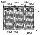
또한, 액정 소자에 전기적으로 접속하는 스위치로서 기능하는 소자를 설치하고, 각각의 액정 소자를 스위치로서 기능하는 소자에 의해 제어할 수 있다. 도 5에 스위치로서 기능하는 소자로서 트랜지스터를 설치하고, 액정 소자를 구동하는 예를 도시한다. Moreover, the element which functions as a switch electrically connected to a liquid crystal element can be provided, and each liquid crystal element can be controlled by the element which functions as a switch. An example in which a transistor is provided as an element functioning as a switch in FIG. 5 to drive a liquid crystal element is shown.
도 5의 셔터 패널에는, 트랜지스터(120a1)와 전기적으로 접속하는 전극(116a1)을 포함하는 제 1 액정 소자, 상기 제 1 액정 소자에 인접하고, 트랜지스터(120a2)와 전기적으로 접속하는 전극(116a2)을 포함하는 제 2 액정 소자, 트랜지스터(120a3)와 전기적으로 접속하는 전극(116a3)을 포함하는 제 3 액정 소자, 용량 배선(124)이 설치된다. 도시하지 않았지만, 전극(116a1, 116a2, 116a3) 위에는 액정을 개재하여 쌍이 되는 전극이 설치된다. In the shutter panel of FIG. 5, a first liquid crystal element including an electrode 116a1 electrically connected to the transistor 120a1, and an electrode 116a2 adjacent to the first liquid crystal element and electrically connected to the transistor 120a2. And a third liquid crystal element including a second liquid crystal element, a third liquid crystal element including an electrode 116a3 electrically connected to the transistor 120a3, and a
배선(121a)과 전기적으로 접속된 트랜지스터(120a1), 트랜지스터(120a2) 및 트랜지스터(120a3)는, 배선(122a1, 122a2, 또는 122a3)과 각각 전기적으로 접속한다. The transistors 120a1, 120a2, and 120a3 electrically connected to the
또한, 도 5에 있어서, 전극(116a1), 전극(116a2), 전극(116a3)의 크기(면적)는 거의 동일한 예를 도시하지만, 특별히 한정되지 않고 전극(116a1), 전극(116a2), 전극(116a3)의 크기는 각각 상이하여도 좋다. 또한, 전극(116a)을 포함하는 액정 소자의 양측에 배치되는 액정 소자는 더욱 다수(3개 이상)라도 좋다. In addition, although the magnitude | size (area) of the electrode 116a1, the electrode 116a2, and the electrode 116a3 shows the substantially same example in FIG. 5, it does not specifically limit, The electrode 116a1, the electrode 116a2, and the electrode ( The size of 116a3) may differ, respectively. In addition, the liquid crystal elements disposed on both sides of the liquid crystal element including the electrode 116a may be more than three (three or more).
3차원 표시를 행할 때, 제 1 액정 소자, 제 2 액정 소자 및 제 3 액정 소자를 제어함으로써, 선택적으로 차광 영역을 결정할 수 있다. 예를 들어, 제 1 액정 소자만 구동하여 형성하는 제 1 차광 영역, 제 1 액정 소자 및 제 2 액정 소자를 구동하여 형성하는 제 2 차광 영역, 또는 제 1 액정 소자, 제 2 액정 소자 및 제 3 액정 소자를 구동하여 형성하는 제 3 차광 영역을 형성할 수 있다. When performing 3D display, a light shielding area can be selectively determined by controlling a 1st liquid crystal element, a 2nd liquid crystal element, and a 3rd liquid crystal element. For example, a first light shielding region formed by driving only a first liquid crystal element, a second light shielding region formed by driving a first liquid crystal element and a second liquid crystal element, or a first liquid crystal element, a second liquid crystal element, and a third A third light blocking region can be formed by driving the liquid crystal element.
셔터 패널(100)을 이와 같이 구동함으로써, 관찰자가 표시 패널에 가까워도, 왼쪽 눈은 왼쪽 눈용의 화소 영역만을, 오른쪽 눈은 오른쪽 눈용의 화소 영역만을 관찰할 수 있게 되어, 3차원 표시를 눈으로 확인할 수 있는 범위가 확대된다. By driving the
또한, 본 실시형태에서는 도시하지 않지만, 셔터 패널에 편광판, 위상차판, 반사 방지막 등의 광학 필름 등이 적절히 설치한다. 셔터 패널은, 다양한 구성의 투과형 액정 소자, 및 다양한 액정 모드를 사용할 수 있다. In addition, although not shown in this embodiment, optical films, such as a polarizing plate, a retardation plate, and an anti-reflective film, etc. are suitably provided in a shutter panel. The shutter panel can use a transmissive liquid crystal element having various configurations and various liquid crystal modes.
예를 들어, 도 4a1 내지 도 4b2에 예시하는 구성과 같이, 한 쌍의 전극이 액정을 협지하는 구성이면, 기판에 개략 수직인 전계를 발생시켜, 기판과 수직인 면 내에서 액정 분자를 움직이게 하여, 계조를 제어하는 방식을 사용할 수 있다. 또한, 도 5에 예시하는 구성에, 액정 소자의 전극을 IPS 모드나 FFS 모드로 사용하는 구성을 적용하고, 기판에 개략 평행(즉 수평인 방향)인 전계를 발생시켜, 기판과 평행인 면 내에서 액정 분자를 움직이게 하여, 계조를 제어하는 방식을 사용할 수 있다. For example, as in the configuration illustrated in FIGS. 4A1 to 4B2, when the pair of electrodes is configured to sandwich the liquid crystal, an approximately perpendicular electric field is generated to move the liquid crystal molecules in a plane perpendicular to the substrate. For example, a method of controlling gray levels may be used. In addition, the structure which uses the electrode of a liquid crystal element in IPS mode or FFS mode is applied to the structure illustrated in FIG. 5, the electric field which is substantially parallel (namely, horizontal direction) is generated in a board | substrate, and it is in-plane parallel to a board | substrate. By moving the liquid crystal molecules in the can be used to control the gray scale.
셔터 패널에 사용하는 트랜지스터의 구조는 특별히 한정되지 않고, 예를 들어 톱 게이트 구조, 또는 보텀 게이트 구조의 스태거형(staggered) 및 플래너형(planar) 등을 사용할 수 있다. 또한, 트랜지스터는 채널 형성 영역이 1개 형성되는 싱글 게이트 구조라도, 2개 형성되는 더블 게이트 구조 또는 3개 형성되는 트리플 게이트 구조라도 좋다. 또한, 채널 형성 영역의 상하에 게이트 절연층을 개재하여 배치된 2개의 게이트 전극층을 갖는, 듀얼 게이트형이어도 좋다. The structure of the transistor used for the shutter panel is not particularly limited, and for example, a staggered, planar or the like of a top gate structure or a bottom gate structure can be used. The transistor may be a single gate structure in which one channel formation region is formed, a double gate structure in which two channels are formed, or a triple gate structure in which three transistors are formed. Alternatively, a dual gate type may be provided having two gate electrode layers disposed above and below the channel formation region via a gate insulating layer.
본 실시형태는, 다른 실시형태에 기재한 구성과 적절히 조합하여 실시할 수 있다. This embodiment can be implemented in appropriate combination with any of the structures described in the other embodiments.
(실시형태 3)(Embodiment 3)
본 실시형태에서는, 실시형태 1에서 도시한 표시 패널에 적용 가능한 표시 패널의 구성예에 관해서 도 6a 및 도 6b, 및 도 7a 및 도 7b를 사용하여 설명한다. In this embodiment, the structural example of the display panel applicable to the display panel shown in
표시 패널에 설치되는 표시 소자로서는, 발광 소자(발광 표시 소자라고도 하다), 액정 소자(액정 표시 소자라고도 한다)를 사용할 수 있다. 발광 소자는, 전류 또는 전압에 의해 휘도가 제어되는 소자를 그 범주에 포함하고 있으며, 구체적으로는 무기 EL(Electro Luminescent) 소자, 유기 EL 소자 등이 포함된다. As a display element provided in a display panel, a light emitting element (also called a light emitting display element) and a liquid crystal element (also called liquid crystal display element) can be used. The light emitting element includes, in its category, an element whose luminance is controlled by current or voltage, and specifically includes an inorganic EL (Electro Luminescent) element, an organic EL element, and the like.
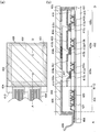
도 6a 및 도 6b에, 표시 소자로서 유기 EL 소자를 적용한 표시 패널의 구성예를 도시한다. 도 6a는 표시 패널의 평면도이며, 도 6b는, 도 6a의 A-B 및 C-D에서의 단면도이다. 소자 기판(410)은, 씰재(405)에 의해 밀봉 기판(404)과 고착되어 있고, 구동 회로부(소스측 구동 회로(401), 게이트측 구동 회로(403)), 복수의 화소를 포함하는 화소부(402)를 갖고 있다. 6A and 6B show a structural example of a display panel in which an organic EL element is applied as a display element. 6A is a plan view of the display panel, and FIG. 6B is a cross-sectional view taken along the lines A-B and C-D of FIG. 6A. The
또한, 배선(408)은 소스측 구동 회로(401) 및 게이트측 구동 회로(403)에 입력되는 신호를 전송하기 위한 배선이며, 외부 입력 단자가 되는 FPC(409, 플렉시블 프린트 서킷(flexible printed circuit))으로부터 비디오 신호, 클럭 신호, 스타트 신호, 리셋 신호 등을 받는다. 또한, 여기서는 FPC만 도시하지만, 이 FPC에는 프린트 배선 기판(PWB)이 부착되어 있어도 좋다. 본 명세서에서의 표시 패널에는, 표시 패널 본체뿐만 아니라, 거기에 FPC 또는 PWB가 부착된 상태도 포함하는 것으로 한다.In addition, the
소자 기판(410) 위에는 구동 회로부(소스측 구동 회로(401), 게이트측 구동 회로(403)) 및 화소부(402)가 형성되어 있다. 도 6b에서는, 구동 회로부인 소스측 구동 회로(401)와, 화소부(402) 중 3개의 화소를 도시한다. On the
본 실시형태에서는, 청색(B)의 화소(420a), 녹색(G)의 화소(420b), 적색(R)의 화소(420c), 3색의 화소를 갖는 예를 도시한다. 또한, 본 실시형태는 이것에 한정되지 않고, 화소부(402)에 적어도 2색 이상의 화소를 포함하는 것으로, 다색 표시를 행하는 표시 패널로 할 수 있다. 또는, 단색 표시를 행하는 표시 패널로 하여도 좋다. In this embodiment, the example which has the
화소(420a, 420b, 420c)는 각각, 컬러 필터층(434a, 434b, 434c)과, 발광 소자(418a, 418b, 418c)와, 상기 발광 소자(418a, 418b, 418c)와 전기적으로 접속하고, 스위칭용 트랜지스터로서 기능하는 트랜지스터(412a, 412b, 412c)를 갖고 있다. 또한, 컬러 필터층(434a, 434b, 434c)을 둘러싸는 블랙 매트릭스(435)가 형성되어 있다. The
컬러 필터층은 각각 각 화소의 색에 대응하여 설치하면 좋고, 예를 들어, 청색(B)의 화소(420a)의 컬러 필터층(434a)을 청색으로 하고, 녹색(G)의 화소(420b)의 컬러 필터층(434b)을 녹색으로 하고, 적색(R)의 화소(420c)의 컬러 필터층(434c)을 적색으로 하면 좋다. What is necessary is just to provide a color filter layer corresponding to the color of each pixel, for example, make the
또한, 발광 소자(418a, 418b, 418c)는 각각 반사성을 갖는 전극(413a, 413b, 413c)과, EL층(431)과, 투광성을 갖는 전극(433)을 갖는다. 반사성을 갖는 전극(413a, 413b, 413c) 및 투광성을 갖는 전극(433)은 한쪽이 양극으로 사용되고, 다른 한쪽이 음극으로서 사용된다. In addition, the
EL층(431)은 적어도 발광층을 갖는다. 또한, EL층(431)은 발광층 이외에 정공 주입층, 정공 수송층, 전자 수송층, 전자 주입층 등을 갖는 적층 구조로 할 수도 있다. 또한, EL층을 복수층 적층시켜도 좋고, EL층의 하나와 다른 EL층 사이에 전하 발생층을 설치하여도 좋다. 또한, 양극과 음극 사이에 발광층을 복수층 적층함으로써, 예를 들어 백색 발광을 나타내는 발광 소자로 할 수 있다. The
또한, 반사성을 갖는 전극(413a, 413b, 413c)과 EL층(431) 사이에, 투광성을 갖는 도전층(415a, 415b, 415c)을 각각 설치하여도 좋다. 상기 투광성을 갖는 도전층(415a, 415b, 415c)은, 각각의 화소에 있어서 반사성을 갖는 전극(413a, 413b, 413c)과 투광성을 갖는 전극(433)의 광학 거리를 조정하는 기능을 갖는다. 각 발광 소자에서 마이크로 캐비티에 의해 원하는 스펙트럼을 증강시킴으로써, 색 순도가 높은 표시 패널을 실현할 수 있다. Further, transparent
또한, 도 6b에서는, 백색 발광하는 발광 소자 및 컬러 필터를 조합한 톱 에미션 구조의 표시 패널(top-emission display panel)에 관해서 설명하였지만, 상기 표시 패널로서, 분리 채색 방식(separate coloring method)에 의해 형성한 발광 소자의 톱 에미션 구조의 표시 패널을 적용하는 것도 가능하다. 또한, 분리 채색 방식이란, 각 화소에 RGB 재료를 증착법 등으로 나누어 칠하는 방식이다. In addition, although FIG. 6B has described the top-emission display panel which combined the light emitting element which emits white light, and a color filter, as the said display panel, it used the separate coloring method. It is also possible to apply the display panel of the top emission structure of the light emitting element formed by this. The separate coloring method is a method of dividing an RGB material into each pixel by a vapor deposition method or the like.
단, 발광층을 화소마다 금속 마스크에 의해 분리 채색하지 않고, 연속막으로 형성함으로써, 금속 마스크를 사용함에 따른 수율의 저하나 공정의 복잡화를 회피할 수 있다. 따라서, 고정밀도로 색 재현성이 높은 표시 패널을 실현하는 것이 가능하게 된다. However, by forming the light emitting layer into a continuous film without separating and coloring each pixel with a metal mask, it is possible to avoid a decrease in yield and complexity of the process due to the use of the metal mask. Therefore, it is possible to realize a display panel with high color reproducibility with high accuracy.
또한, 소스측 구동 회로(401)는 n-채널형 트랜지스터(423)와 p-채널형 트랜지스터(424)를 조합한 CMOS 회로가 형성된다. 또한, 게이트측 구동 회로(403)는, 트랜지스터로 형성되는 각종의 CMOS 회로, PMOS 회로 또는 NMOS 회로로 형성하여 좋다. 또한, 본 실시형태에서는, 기판 위에 소스측 구동 회로 및 게이트측 구동 회로를 형성하는 예를 나타내지만, 반드시 그럴 필요는 없고, 소스측 구동 회로 및 게이트측 구동 회로의 일부, 또는 전부를 기판 위에서가 아니라 외부에 형성할 수도 있다. In the source
또한, 반사성을 갖는 전극(413a, 413b, 413c) 및 투광성을 갖는 도전층(415a, 415b, 415c)의 단부를 덮어 절연물(414)이 형성되어 있다. 여기서는, 포지티브형의 감광성 아크릴 수지막을 사용함으로써 형성할 수 있다. In addition, an insulator 414 is formed by covering the ends of the reflective electrodes 413a, 413b, and 413c and the transmissive
또한, 피복성을 양호한 것으로 하기 위해서, 절연물(414)의 상단부 또는 하단부에 곡률을 갖는 곡면이 형성되도록 한다. 예를 들어, 절연물(414)의 재료로서 포지티브형의 감광성 아크릴을 사용한 경우, 절연물(414)의 상단부에만 곡률 반경(0.2㎛~3㎛)을 갖는 곡면을 갖게 하는 것이 바람직하다. 또한, 절연물(414)로서, 빛의 조사에 의해 에칭액에 불용해성이 되는 네거티브형, 또는 빛의 조사에 의해 에칭액에 용해성이 되는 포지티브형 모두를 사용할 수 있다. In addition, in order to make the coating | cover property favorable, the curved surface which has curvature is formed in the upper end part or lower end part of the insulator 414. For example, when positive type photosensitive acrylic is used as a material of the insulator 414, it is preferable to have a curved surface having a radius of curvature (0.2 μm to 3 μm) only at the upper end of the insulator 414. As the insulator 414, both a negative type that is insoluble in the etching solution by irradiation of light or a positive type that is soluble in the etching solution by irradiation of light can be used.
또한, 씰재(405)로 밀봉 기판(404)을 소자 기판(410)과 부착함으로써, 소자 기판(410), 밀봉 기판(404) 및 씰재(405)로 둘러싸인 공간(407)에 발광 소자(418a, 418b, 418c)가 구비된 구조로 되어 있다. 또한, 공간(407)에는 충전재가 충전되어 있고, 불활성 기체(질소나 아르곤 등)가 충전되는 경우 이외에, 유기 수지, 씰재(405)로 충전되는 경우도 있다. 유기 수지 및 씰재(405)에는 흡습성을 갖는 물질을 포함하는 재료를 사용하여도 좋다. In addition, the sealing
또한, 씰재(405)에는 에폭시계 수지를 사용하는 것이 바람직하다. 또한, 이들 재료는 가능한 한 수분이나 산소를 투과하지 않는 재료인 것이 바람직하다. 또한, 밀봉 기판(404)에 사용하는 재료로서 유리 기판이나 석영 기판 이외에, FRP(Fiberglass-Reinforced Plastics), PVF(불화 비닐 수지), 폴리에스테르 또는 아크릴 등으로 이루어진 플라스틱 기판을 사용할 수 있다. In addition, it is preferable to use an epoxy resin for the sealing
본 실시형태와 같이, 하지막이 되는 절연막(411)을 소자 기판(410)과 트랜지스터의 반도체층 사이에 설치하여도 좋다. 절연막은, 소자 기판(410)으로부터의 불순물 원소의 확산을 방지하는 기능이 있고, 질화실리콘막, 산화실리콘막, 질화산화실리콘막, 또는 산화질화실리콘막 중에서 선택된 하나 또는 복수의 막에 의한 단층, 또는 적층 구조에 의해 형성할 수 있다. As in the present embodiment, an insulating
본 실시형태에 있어서, 표시 패널에 적용할 수 있는 트랜지스터의 구조는 특별히 한정되지 않고, 예를 들어 톱 게이트 구조, 또는 보텀 게이트 구조의 스태거형 및 플래너형 등을 사용할 수 있다. 또한, 트랜지스터는 채널 형성 영역이 1개 형성되는 싱글 게이트 구조라도, 2개 형성되는 더블 게이트 구조 또는 3개 형성되는 트리플 게이트 구조라도 좋다. 또한, 채널 형성 영역의 상하에 게이트 절연층를 개재하여 배치된 2개의 게이트 전극층을 갖는 듀얼 게이트형이라도 좋다. In the present embodiment, the structure of the transistor that can be applied to the display panel is not particularly limited, and for example, a top gate structure, a staggered type and a planar type of a bottom gate structure can be used. The transistor may be a single gate structure in which one channel formation region is formed, a double gate structure in which two channels are formed, or a triple gate structure in which three transistors are formed. Alternatively, a dual gate type may be provided having two gate electrode layers disposed above and below the channel formation region via a gate insulating layer.
게이트 전극층의 재료는, 몰리브덴, 티타늄, 크롬, 탄탈, 텅스텐, 알루미늄, 구리, 네오디뮴, 스칸듐 등의 금속 재료 또는 이들을 주성분으로 하는 합금 또는 화합물을 사용하여, 단층으로 또는 적층하여 형성할 수 있다. The material of the gate electrode layer can be formed in a single layer or laminated by using a metal material such as molybdenum, titanium, chromium, tantalum, tungsten, aluminum, copper, neodymium, scandium, or an alloy or compound containing these as a main component.
예를 들어, 게이트 전극층의 2층의 적층 구조로서는, 알루미늄층 위에 몰리브덴층이 적층된 2층의 적층 구조, 또는 구리층 위에 몰리브덴층을 적층한 2층 구조, 또는 구리층 위에 질화티타늄층 또는 질화탄탈층을 적층한 2층 구조, 질화티타늄층과 몰리브덴층을 적층한 2층 구조로 하는 것이 바람직하다. 3층의 적층 구조로서는, 텅스텐층 또는 질화텅스텐층과, 알루미늄과 실리콘의 합금층 또는 알루미늄과 티타늄의 합금층과, 질화티타늄층 또는 티타늄층을 적층한 적층 구조로 하는 것이 바람직하다. For example, as a laminated structure of two layers of a gate electrode layer, a two-layer laminated structure in which a molybdenum layer is laminated on an aluminum layer, or a two-layer structure in which a molybdenum layer is laminated on a copper layer, or a titanium nitride layer or a nitride layer on a copper layer It is preferable to set it as the two-layer structure which laminated | stacked the tantalum layer, and the two-layer structure which laminated | stacked the titanium nitride layer and the molybdenum layer. As a three-layer laminated structure, it is preferable to set it as the laminated structure which laminated | stacked the tungsten layer or the tungsten nitride layer, the alloy layer of aluminum and silicon, or the alloy layer of aluminum and titanium, and the titanium nitride layer or the titanium layer.
게이트 절연층은, 플라즈마 CVD법 또는 스퍼터링법 등을 사용하여, 산화실리콘층, 질화실리콘층, 산화질화실리콘층 또는 질화산화실리콘층을 단층으로 또는 적층하여 형성할 수 있다. 또한, 게이트 절연층으로서, 유기 실란 가스를 사용한 CVD법에 의해 산화실리콘층을 형성할 수도 있다. 유기 실란 가스로서는, 규산에틸(TEOS: 화학식 Si(OC2H5)4), 테트라메틸실란(TMS: 화학식 Si(CH3)4), 테트라메틸시클로테트라실록산(TMCTS), 옥타메틸시클로테트라실록산(OMCTS), 헥사메틸디실라잔(HMDS), 트리에톡시실란(SiH(OC2H5)3), 트리스디메틸아미노실란(SiH(N(CH3)2)3) 등의 실리콘 함유 화합물을 사용할 수 있다. The gate insulating layer can be formed by laminating a silicon oxide layer, a silicon nitride layer, a silicon oxynitride layer, or a silicon nitride oxide layer using a plasma CVD method, a sputtering method, or the like as a single layer. As the gate insulating layer, a silicon oxide layer can also be formed by a CVD method using an organic silane gas. Examples of the organosilane gas include ethyl silicate (TEOS: chemical formula Si (OC 2 H 5 ) 4 ), tetramethylsilane (TMS: chemical formula Si (CH 3 ) 4 ), tetramethylcyclotetrasiloxane (TMCTS), octamethylcyclotetrasiloxane Silicon-containing compounds such as (OMCTS), hexamethyldisilazane (HMDS), triethoxysilane (SiH (OC 2 H 5 ) 3 ), and trisdimethylaminosilane (SiH (N (CH 3 ) 2 ) 3 ); Can be used.
반도체층에 사용하는 재료는 특별히 한정되지 않고, 트랜지스터(412a, 412b, 412c, 423, 424)에 요구되는 특성에 따라서 적절히 설정하면 좋다. 반도체층에 사용할 수 있는 재료의 예를 설명한다. The material used for a semiconductor layer is not specifically limited, What is necessary is just to set suitably according to the characteristic calculated | required by the
반도체층을 형성하는 재료로서는, 실란이나 게르만으로 대표되는 반도체 재료 가스를 사용한 기상 성장법이나, 스퍼터링법으로 제작된다. 비정질(아모퍼스(amorphous)라고도 한다) 반도체, 상기 비정질 반도체를 광 에너지나 열에너지를 사용하여 결정화시킨 다결정 반도체, 또는 미결정 반도체 등을 사용할 수 있다. 반도체층은 스퍼터링법, LPCVD법, 또는 플라즈마 CVD법 등에 의해 성막할 수 있다. As a material which forms a semiconductor layer, it is produced by the vapor-phase growth method using the semiconductor material gas represented by silane and germane, or the sputtering method. Amorphous (also called amorphous) semiconductors, polycrystalline semiconductors or microcrystalline semiconductors in which the amorphous semiconductors are crystallized using light energy or thermal energy can be used. The semiconductor layer can be formed by a sputtering method, an LPCVD method, a plasma CVD method, or the like.
반도체층으로서, 실리콘이나 탄화실리콘 등의 단결정 반도체를 사용할 수 있다. 반도체층으로서 단결정 반도체를 사용하면, 트랜지스터 사이즈를 미세화하는 것이 가능하게 되기 때문에, 표시부에 있어서 화소를 더욱 고정세화할 수 있다. 반도체층으로서 단결정 반도체를 사용하는 경우에는, 단결정 반도체층이 설치된 SOI 기판을 적용할 수 있다. 또는, 실리콘 웨이퍼 등의 반도체 기판을 사용하여도 좋다. As the semiconductor layer, a single crystal semiconductor such as silicon or silicon carbide can be used. When a single crystal semiconductor is used as the semiconductor layer, the size of the transistor can be reduced, so that the pixel can be further refined in the display portion. In the case of using a single crystal semiconductor as the semiconductor layer, an SOI substrate provided with a single crystal semiconductor layer can be applied. Alternatively, a semiconductor substrate such as a silicon wafer may be used.
비정질 반도체로서는, 대표적으로 수소화 비정질 실리콘, 결정성 반도체로서는 대표적으로 폴리실리콘 등을 들 수 있다. 폴리실리콘(다결정 실리콘)에는, 800℃ 이상의 프로세스 온도를 거쳐 형성되는 폴리실리콘을 주재료로서 사용한 소위 고온 폴리실리콘이나, 600℃ 이하의 프로세스 온도로 형성되는 폴리실리콘을 주재료로서 사용한 소위 저온 폴리실리콘, 또한 결정화를 촉진하는 원소 등을 사용하여, 비정질 실리콘을 결정화시킨 폴리실리콘 등을 포함한다. 물론, 상기한 바와 같이, 미결정 반도체 또는 반도체층의 일부에 결정상을 포함하는 반도체를 사용할 수도 있다. Typical examples of the amorphous semiconductor include hydrogenated amorphous silicon and typical examples of the crystalline semiconductor include polysilicon and the like. In polysilicon (polycrystalline silicon), so-called high-temperature polysilicon using polysilicon formed through a process temperature of 800 ° C or higher as a main material, or so-called low-temperature polysilicon using polysilicon formed at a process temperature of 600 ° C or lower as a main material, and Polysilicon etc. which crystallized amorphous silicon using the element etc. which promote crystallization are included. Of course, as described above, a microcrystalline semiconductor or a semiconductor containing a crystalline phase in a part of the semiconductor layer may be used.
또한, 산화물 반도체를 사용하여도 좋고, 산화물 반도체로서는, 4원계 금속 산화물인 In-Sn-Ga-Zn-O계나, 3원계 금속 산화물인 In-Ga-Zn-O계, In-Sn-Zn-O계, In-Al-Zn-O계, Sn-Ga-Zn-O계, Al-Ga-Zn-O계, Sn-Al-Zn-O계나, 2원계 금속 산화물인 In-Zn-O계, Sn-Zn-O계, Al-Zn-O계, Zn-Mg-O계, Sn-Mg-O계, In-Mg-O계, In-Ga-O계나, In-O계, Sn-O계, Zn-O계 등을 사용할 수 있다. 또한, 상기 산화물 반도체에 SiO2를 함유하여도 좋다. 여기서, 예를 들어, In-Ga-Zn-O계 산화물 반도체란, 적어도 In과 Ga와 Zn을 함유하는 산화물이며, 그 조성비에 특별히 한정은 없다. 또한, In과 Ga와 Zn 이외의 원소를 함유하여도 좋다. In addition, an oxide semiconductor may be used, and examples of the oxide semiconductor include an In—Sn—Ga—Zn—O system, which is a quaternary metal oxide, or an In—Ga—Zn—O, In—Sn—Zn—, which is a ternary metal oxide. O-based, In-Al-Zn-O-based, Sn-Ga-Zn-O-based, Al-Ga-Zn-O-based, Sn-Al-Zn-O-based, or In-Zn-O-based binary metal oxides , Sn-Zn-O-based, Al-Zn-O-based, Zn-Mg-O-based, Sn-Mg-O-based, In-Mg-O-based, In-Ga-O-based, In-O-based, Sn- O system, Zn-O system, etc. can be used. Further, SiO 2 may be contained in the oxide semiconductor. Here, for example, an In—Ga—Zn—O based oxide semiconductor is an oxide containing at least In, Ga, and Zn, and the composition ratio is not particularly limited. Moreover, you may contain elements other than In, Ga, and Zn.
또한, 산화물 반도체층은, 화학식 InMO3(ZnO)m(m>0)로 표기되는 박막을 사용할 수 있다. 여기서, M은, Ga, Al, Mn 및 Co 중에서 선택된 하나 또는 복수의 금속 원소를 나타낸다. 예를 들어 M으로서, Ga, Ga 및 Al, Ga 및 Mn, 또는 Ga 및 Co 등이 있다. As the oxide semiconductor layer, a thin film represented by the formula InMO 3 (ZnO) m (m> 0) can be used. Here, M represents one or a plurality of metal elements selected from Ga, Al, Mn, and Co. For example, as M, there are Ga, Ga and Al, Ga and Mn, or Ga and Co.
또한, 산화물 반도체로서 In-Zn-O계의 재료를 사용하는 경우, 원자수비(atomic ratio)로, In/Zn=0.5~50, 바람직하게는 In/Zn=1~20, 더욱 바람직하게는 In/Zn=1.5~15로 한다. Zn에 대한 In의 원자수비를 바람직하게 상기 범위로 함으로써, 트랜지스터의 전계 효과 이동도를 향상시킬 수 있다. 여기서, 화합물의 원자수비가 In: Zn: O=X: Y:Z일 때, Z>1.5X+Y로 한다. In the case of using an In—Zn—O-based material as the oxide semiconductor, In / Zn = 0.5 to 50, preferably In / Zn = 1 to 20, more preferably In, in atomic ratio. / Zn = 1.5 to 15. By setting the atomic ratio of In to Zn in the above range, the field effect mobility of the transistor can be improved. Here, when the atomic number ratio of the compound is In: Zn: O = X: Y: Z, let Z> 1.5X + Y.
산화물 반도체층으로서, 단결정 구조도 아니고, 비정질 구조도 아닌 구조이며, C축 배향을 가진 결정성 산화물 반도체(C Axis Aligned Crystalline Oxide Semiconductor; CAAC-OS라고도 불린다)를 사용할 수 있다. As the oxide semiconductor layer, a crystalline oxide semiconductor (also referred to as CAAC-OS), which is neither a single crystal nor an amorphous structure and has a C-axis orientation, can be used.
소스 전극층 또는 드레인 전극층으로서 기능하는 배선층의 재료로서는, Al, Cr, Ta, Ti, Mo, W에서 선택된 원소, 또는 상기한 원소를 성분으로 하는 합금이나, 상기한 원소를 조합한 합금 등을 들 수 있다. 또한, 열처리를 행하는 경우에는, 이 열처리에 견디는 내열성을 도전막에 갖게 하는 것이 바람직하다. 예를 들어, Al단체에서는 내열성이 약하고, 또한 부식하기 쉬운 등의 문제점이 있으므로 내열성 도전성 재료와 조합하여 형성한다. Al과 조합하는 내열성 도전성 재료로서는, 티타늄(Ti), 탄탈(Ta), 텅스텐(W), 몰리브덴(Mo), 크롬(Cr), 네오디뮴(Nd), 스칸듐(Sc)에서 선택된 원소, 또는 상기한 원소를 성분으로 하는 합금이나, 상기한 원소를 조합한 합금, 또는 상기한 원소를 성분으로 하는 질화물로 형성한다. As a material of the wiring layer which functions as a source electrode layer or a drain electrode layer, the element selected from Al, Cr, Ta, Ti, Mo, W, the alloy which makes the above element a component, the alloy which combined said element, etc. are mentioned. have. In addition, in the case of performing heat treatment, it is preferable to give the conductive film heat resistance to withstand this heat treatment. For example, Al has a problem such as weak heat resistance and easy corrosion, and is formed in combination with a heat resistant conductive material. As the heat resistant conductive material combined with Al, an element selected from titanium (Ti), tantalum (Ta), tungsten (W), molybdenum (Mo), chromium (Cr), neodymium (Nd), scandium (Sc), or the aforementioned It forms from the alloy which has an element as a component, the alloy which combined said element, or the nitride which has the said element as a component.
트랜지스터를 덮는 절연막(419)은, 건식법이나 습식법으로 형성되는 무기 절연막, 유기 절연막을 사용할 수 있다. 예를 들어, CVD법이나 스퍼터링법 등을 사용하여 얻어지는 질화실리콘막, 산화실리콘막, 산화질화실리콘막, 산화알루미늄막, 산화탄탈막, 산화갈륨막 등을 사용할 수 있다. 또한, 폴리이미드, 아크릴, 벤조사이클로부텐, 폴리아미드, 에폭시 등의 유기 재료를 사용할 수 있다. 또한 상기 유기재료 이외에, 저유전율 재료(low-k 재료), 실록산계 수지, PSG(인 유리), BPSG(인붕소 유리) 등을 사용할 수 있다. As the insulating
또한, 실록산계 수지로는, 실록산계 재료를 출발 재료로서 형성된 Si-O-Si 결합을 포함하는 수지에 상당한다. 실록산계 수지는 치환기로서 유기기(예를 들어 알킬기나 아릴기)나 플루오르기를 사용하여도 좋다. 또한, 유기기는 플루오르기를 가져도 좋다. 실록산계 수지는 도포법에 의해 성막하고, 소성함으로써 절연막(419)으로서 사용할 수 있다. In addition, as a siloxane resin, it corresponds to resin containing the Si-O-Si bond formed from the siloxane material as a starting material. The siloxane-based resin may use an organic group (for example, an alkyl group or an aryl group) or a fluorine group as a substituent. In addition, the organic group may have a fluorine group. The siloxane-based resin is formed by a coating method and can be used as the insulating
또한, 이들 재료로 형성되는 절연막을 복수 적층시킴으로써, 절연막(419)을 형성하여도 좋다. 예를 들어, 무기 절연막 위에 유기 수지막을 적층하는 구조으로 하여도 좋다. In addition, the insulating
도 7a 및 도 7b에 표시 소자로서 액정 소자를 사용한 표시 패널의 예를 도시한다. 도 7a는 표시 패널의 평면도이며, 도 7b는 도 7a의 E-F에 따른 단면도이다. 또한, 본 실시형태에서 도시한 액정 소자를 포함하는 패널은 셔터 패널의 구성에 적절히 사용할 수 있다. 7A and 7B show examples of display panels using liquid crystal elements as display elements. 7A is a plan view of the display panel, and FIG. 7B is a cross-sectional view taken along line E-F of FIG. 7A. In addition, the panel containing the liquid crystal element shown in this embodiment can be used suitably for the structure of a shutter panel.
도 7b에 있어서, 제 1 기판(601) 위에 설치된 화소부(602)와, 주사선 구동 회로(604)를 둘러싸도록 하여, 씰재(605)가 설치된다. 또한 화소부(602)와, 주사선 구동 회로(604) 위에 제 2 기판(606)이 설치된다. 따라서, 화소부(602)와, 주사선 구동 회로(604)는, 제 1 기판(601)과 씰재(605)와 제 2 기판(606)에 의해, 표시 소자와 함께 밀봉된다. In FIG. 7B, a
도 7a에 있어서는, 제 1 기판(601) 위의 씰재(605)에 의해 둘러싸여 있는 영역과는 다른 영역에, 별도로 준비된 기판 위에 단결정 반도체막 또는 다결정 반도체막으로 형성된 신호선 구동 회로(603)가 실장되어 있다. 신호선 구동 회로(603)와, 주사선 구동 회로(604) 또는 화소부(602)에 주어진 각종 신호 및 전위는 FPC(618)에서 공급된다. In FIG. 7A, a signal
도 7a 및 도 7b에 있어서, 표시 패널은, 접속 단자 전극(615) 및 단자 전극(616)을 갖고, 접속 단자 전극(615) 및 단자 전극(616)은 FPC(618)가 갖는 단자와 이방성 도전막(619)을 통하여 전기적으로 접속된다. 접속 단자 전극(615)은 액정 소자의 제 1 전극층(630)과 동일한 도전막으로 형성되고, 단자 전극(616)은 트랜지스터(610), 트랜지스터(611)의 소스 전극 및 드레인 전극과 동일한 도전막으로 형성되어 있다. In FIGS. 7A and 7B, the display panel has a connecting
또한, 제 1 기판(601) 위에 설치된 화소부(602)와, 주사선 구동 회로(604)는 트랜지스터를 복수 갖고 있고, 도 7b에서는, 화소부(602)에 포함되는 트랜지스터(610)와, 주사선 구동 회로(604)에 포함되는 트랜지스터(611)를 예시한다. In addition, the
도 7b에 있어서, 표시 소자인 액정 소자(613)는 제 1 전극층(630), 제 2 전극층(631) 및 액정층(608)을 포함한다. 또한, 액정층(608)을 협지하도록 배향막으로서 기능하는 절연막(632, 633)이 설치된다. 제 2 전극층(631)은 제 2 기판(606)측에 설치되고, 제 1 전극층(630)과 제 2 전극층(631)은 액정층(608)를 개재하여 적층하는 구성으로 되어 있다. In FIG. 7B, the
또한, 기둥 형상의 스페이서(635)는 절연막을 선택적으로 에칭함으로써 얻어진다. 액정층(608)의 막 두께(셀 갭)를 제어하기 위해서 설치된다. 또한, 구 형상의 스페이서를 사용하여도 좋다. The
표시 소자로서, 액정 소자를 사용하는 경우, 서모트로픽(thermotropic) 액정, 저분자 액정, 고분자 액정, 고분자 분산형 액정, 강유전성 액정, 반강유전성 액정 등을 사용할 수 있다. 이들 액정 재료는, 조건으로 콜레스테릭상(cholesteric phase), 스메틱상(smectic phase), 큐빅상, 키랄네마틱상(chiral nematic phase), 등방상(isotropic phase) 등을 나타낸다. As the display element, a thermotropic liquid crystal, a low molecular liquid crystal, a polymer liquid crystal, a polymer dispersed liquid crystal, a ferroelectric liquid crystal, an antiferroelectric liquid crystal, or the like can be used. These liquid crystal materials exhibit cholesteric phase, smectic phase, cubic phase, chiral nematic phase, isotropic phase and the like under conditions.
또한, 배향막을 사용하지 않는 블루상(blue phase)을 나타내는 액정을 사용하여도 좋다. 블루상은 액정상의 하나이며, 콜레스테릭 액정을 승온하면, 콜레스테릭상으로부터 등방상으로 전이하기 직전에 발현되는 상이다. 블루상은 좁은 온도 범위에서만 발현되기 때문에, 온도 범위를 넓히기 위해서 수 중량% 이상의 키랄제를 혼합한 액정 조성물을 사용하여 액정층에 사용한다. 블루상을 나타내는 액정과 키랄제를 포함하는 액정 조성물은, 응답 속도가 1msec 이하로 짧고, 광학적 등방성이기 때문에 배향 처리가 필요하지 않고, 시야각 의존성이 작다. 또한 배향막을 설치하지 않아도 좋으므로 러빙 처리(rubbing treatment)도 필요하지 않기 때문에, 러빙 처리로 야기되는 정전 파괴를 방지할 수 있고, 제작 공정 중의 표시 패널의 불량이나 파손을 경감할 수 있다. 따라서, 표시 패널의 생산성을 향상시키는 것이 가능하게 된다. Moreover, you may use the liquid crystal which shows the blue phase which does not use an alignment film. The blue phase is one of the liquid crystal phases, and when the cholesteric liquid crystal is heated, the blue phase is a phase which is expressed immediately before transition from the cholesteric phase to the isotropic phase. Since a blue phase is expressed only in a narrow temperature range, in order to expand a temperature range, it uses for the liquid crystal layer using the liquid crystal composition which mixed several weight% or more of chiral agents. The liquid crystal composition containing a liquid crystal and a chiral agent exhibiting a blue phase has a short response speed of 1 msec or less, and because of its optical isotropy, no alignment treatment is required, and the viewing angle dependency is small. In addition, since the alignment film does not need to be provided, no rubbing treatment is required, so that electrostatic breakdown caused by the rubbing treatment can be prevented, and defects or breakage of the display panel during the manufacturing process can be reduced. Therefore, it is possible to improve the productivity of the display panel.
또한, 액정 재료의 고유 저항률은, 1×10⁹Ωㆍ㎝ 이상이며, 바람직하게는 1×10¹¹Ωㆍ㎝ 이상이며, 더욱 바람직하게는 1×10¹²Ωㆍ㎝ 이상이다. 또한, 본 명세서에서의 고유 저항률의 값은 20℃에서 측정한 값으로 한다. The resistivity of the liquid crystal material is 1 × 10 9 Ω · cm or more, preferably 1 × 10 11 Ω · cm or more, and more preferably 1 × 10 12 Ω · cm or more. In addition, the value of the specific resistivity in this specification shall be the value measured at 20 degreeC.
액정 소자를 갖는 표시 패널(액정표시 패널)에는, TN(Twisted Nematic) 모드, IPS(In-Plane-Switching) 모드, FFS(Fringe Field Switching) 모드, ASM(Axially Symmetric Aligned Micro-cell) 모드, OCB(Optically Compensated Birefringence) 모드, FLC(Ferroelectric Liquid Crystal) 모드, AFLC(AntiFerroelectric Liquid Crystal) 모드 등을 사용할 수 있다. In a display panel (liquid crystal display panel) having a liquid crystal element, a twisted nematic (TN) mode, an in-plane-switching (IPS) mode, a fringe field switching (FSF) mode, an symmetrically aligned micro-cell (ASM) mode, and an OCB (Optically Compensated Birefringence) mode, FLC (Ferroelectric Liquid Crystal) mode, AFLC (AntiFerroelectric Liquid Crystal) mode, and the like can be used.
또한, 노멀리 블랙(normally black)형의 액정 표시 패널, 예를 들어 수직 배향(VA) 모드를 채용한 투과형의 액정 표시 패널로 하여도 좋다. 여기서, 수직 배향 모드란, 액정 표시 패널의 액정 분자의 배열을 제어하는 방식의 일종이며, 전압이 인가되지 않을 때에 패널면에 대하여 액정 분자가 수직 방향을 향하는 방식이다. 수직 배향 모드로서는, 몇 가지를 들 수 있지만, 예를 들어, MVA(Multi-Domain Vertical Alignment) 모드, PVA(Patterned Vertical Alignment) 모드, ASV(Advanced Super View) 모드 등을 사용할 수 있다. 또한, 화소(픽셀)를 여러 영역(서브 픽셀)으로 나누고, 각각 별개의 방향으로 분자를 정렬(align)하도록 고안된 멀티 도메인화 또는 멀티 도메인 설계라고 물리는 방법을 사용할 수 있다. Further, a normally black liquid crystal display panel, for example, a transmissive liquid crystal display panel employing a vertical alignment (VA) mode may be used. Here, the vertical alignment mode is a kind of method of controlling the arrangement of liquid crystal molecules of the liquid crystal display panel, and is a system in which the liquid crystal molecules are directed in a vertical direction with respect to the panel surface when no voltage is applied. Some examples of the vertical alignment mode include a multi-domain vertical alignment (MVA) mode, a patterned vertical alignment (PVA) mode, an advanced super view (ASV) mode, and the like. It is also possible to use a method of dividing a pixel (pixel) into regions (subpixels), referred to as multi-domainization or multi-domain design, each designed to align molecules in separate directions.
또한, 본 실시형태에서 나타내는 표시 패널에 있어서, 블랙 메트릭스(차광층), 편광 부재, 위상차 부재, 반사 방지 부재 등의 광학 부재(광학 기판) 등은 적절히 설치한다. 예를 들어, 편광 기판 및 위상차 기판에 의한 원 편광을 사용하여도 좋다. 또한, 액정 표시 패널의 광원으로서 백 라이트, 사이드 라이트 등을 사용하여도 좋다. In addition, in the display panel shown in this embodiment, optical members (optical substrates), such as a black matrix (light shielding layer), a polarizing member, a retardation member, an antireflection member, etc. are provided suitably. For example, circularly polarized light by a polarizing substrate and a phase difference substrate may be used. Moreover, you may use a backlight, a side light, etc. as a light source of a liquid crystal display panel.
또한, 화소부에서의 표시 방식은, 프로그레시브 방식이나 인터레이스(interlace) 방식 등을 사용할 수 있다. 또한, 컬러 표시할 때에 화소에서 제어하는 색 요소로서는, RGB(R은 적색, G는 녹색, B는 청색을 나타낸다)의 3색에 한정되지 않는다. 예를 들어, RGBW(W는 백색을 나타낸다), 또는 RGB에 황색, 시안(cyan), 마젠타(magenta) 등을 한가지 색 이상 추가한 것이 있다. 또한, 색 요소의 도트마다 그 표시 영역의 크기가 상이하여도 좋다. 단, 본 실시형태는 컬러 표시의 표시 패널에 한정되는 것이 아니라, 모노 크롬 표시의 표시 패널에 적용할 수도 있다. As the display method in the pixel portion, a progressive method, an interlace method, or the like can be used. In addition, it is not limited to three colors of RGB (R represents red, G represents green, B represents blue) as a color element controlled by a pixel at the time of color display. For example, RGBW (W represents white) or RGB, yellow, cyan, magenta, or the like is added in one or more colors. In addition, the size of the display area may be different for each dot of the color element. However, the present embodiment is not limited to the display panel of the color display, but can also be applied to the display panel of the monochrome display.
이상에서 나타낸 본 실시형태의 표시 패널을, 실시형태1에서 나타낸 표시 패널로서 적용함으로써, 본 발명의 일 형태의 표시 장치를 얻을 수 있다. The display device of one embodiment of the present invention can be obtained by applying the display panel of the present embodiment described above as the display panel shown in the first embodiment.
또한, 본 실시형태는 다른 실시형태에 기재한 구성과 적절히 조합하여 실시할 수 있다. In addition, this embodiment can be implemented in appropriate combination with the structure described in other embodiment.
(실시형태 4)(Fourth Embodiment)
본 발명의 일 형태의 표시 장치는, 터치 패널로 불리는 위치 입력 장치를 가져도 좋다. 본 실시형태에서는, 본 발명의 일 형태의 표시 장치에 적용 가능한 셔터 패널로, 터치 패널을 구비하는 셔터 패널의 구성예를, 도 8a 및 도 8b를 사용하여 설명한다. The display device of one embodiment of the present invention may have a position input device called a touch panel. In this embodiment, a configuration example of a shutter panel including a touch panel as a shutter panel applicable to the display device of one embodiment of the present invention will be described with reference to FIGS. 8A and 8B.
도 8a에 본 실시형태에서 나타낸 셔터 패널의 사시도를 도시한다. 또한, 도 8b에 도 8a의 M-N에서의 단면도를 도시한다. 또한, 도 8a에서는 도면의 번잡을 피하기 위하여, 구성 요소의 일부(예를 들어, 편광판 등)을 생략하여 도시한다. 8A is a perspective view of the shutter panel shown in this embodiment. 8B is a cross sectional view taken along the line M-N in FIG. 8A. In addition, in order to avoid the trouble of drawing in FIG. 8A, some components (for example, a polarizing plate etc.) are abbreviate | omitted and shown.
도 8a 및 도 8b에 도시한 셔터 패널(640)은, 제 1 편광판(642)과, 액정 소자 유닛(650)과, 액정 소자 유닛(650)에 중첩하여 설치된 터치 패널 유닛(660)과 제 2 편광판(648)과, 제 2 편광판(648)에 접하여 설치된 기판(652)을 갖는다. The
액정 소자 유닛(650)은, 복수의 액정 소자를 갖고, 상기 복수의 액정 소자는 기판(644)과 기판(646) 사이에 설치된다. 복수의 액정 소자의 구성은, 상기 실시형태 2에 나타낸 구성을 적용할 수 있다.The liquid
도 8b에 있어서, 화살표는 빛이 방출되는 방향을 나타낸다. 따라서, 본 발명의 일 형태의 표시 장치에 있어서는, 제 1 편광판(642) 측에 표시 패널이 배치된다. In Fig. 8B, the arrow indicates the direction in which light is emitted. Therefore, in the display device of one embodiment of the present invention, the display panel is disposed on the side of the first
터치 패널 유닛(660)으로서는, 예를 들어 정전 용량 방식을 적용할 수 있다. 도 8a 및 도 8b에서는, 정전 용량 방식 중, 투영 정전 용량 방식을 사용하는 구성예를 도시한다. 터치 패널 유닛(660)은, 복수의 제 1 전극(662)과, 제 1 전극(662)을 덮는 절연층(666)과, 복수의 제 2 전극(664)과, 제 2 전극(664)을 덮는 절연층(668)을 갖는다. As the
각각의 제 1 전극(662)은, 직사각 형상의 도전막(661)이 복수 접속된 구성을 갖고, 각각의 제 2 전극(664)은, 직사각 형상의 도전막(663)이 복수 접속된 구성을 갖는다. 또한, 복수의 제 1 전극(662)과 복수의 제 2 전극(664)은, 직사각 형상의 도전막(661)과 직사각 형상의 도전막(663)의 위치가 서로 엇갈리도록 겹쳐져 있다. 또한, 제 1 전극(662)과 제 2 전극(664)의 형상은 이 구성에 한정되지 않는다. Each
제 1 전극(662)과 제 2 전극(664)은, 투광성을 갖는 도전 재료, 예를 들어, 산화 규소를 함유하는 산화인듐주석(ITSO), 산화인듐주석(ITO), 산화아연(ZnO), 산화인듐아연, 갈륨을 첨가한 산화아연(GZO) 등으로 형성할 수 있다. The
본 실시형태에 나타내는 터치 패널 유닛을 갖는 셔터 패널의 일 예는, 셔터 패널을 구성하는 제 1 편광판(642)과 제 2 편광판(648) 사이에 터치 패널 유닛(660)을 적층시킨 구조이다. 상기 구조로 함으로써, 표시 장치에 있어서 셔터 패널과, 터치 패널을 별개로 제작하여 배치하는 경우와 비교하여 부품수를 삭감할 수 있다. 따라서, 표시 장치의 제조 비용을 삭감할 수 있다. 또한, 표시 장치의 경량화 및 박형화를 도모할 수 있다. An example of the shutter panel which has a touch panel unit shown in this embodiment is the structure which laminated | stacked the
또한, 본 실시형태는 다른 실시형태에 기재한 구성과 적절히 조합하여 실시할 수 있다. In addition, this embodiment can be implemented in appropriate combination with the structure described in other embodiment.
(실시형태 5)(Embodiment 5)
본 발명의 일 형태에 따른 표시 장치는, 노트형 퍼스널 컴퓨터, 기록 매체를 구비한 화상 재생 장치(대표적으로는 DVD: Digital Versatile Disc 등의 기록 매체를 재생하고, 그 화상을 표시할 수 있는 디스플레이를 갖는 장치)에 사용할 수 있다. 그 이외에, 본 발명의 일 형태에 따른 표시 장치를 사용할 수 있는 전자 기기로서, 휴대 전화, 휴대형 게임기, 휴대 정보 단말, 전자 서적, 비디오 카메라, 디지털 스틸 카메라, 고글형 디스플레이(헤드 마운트 디스플레이), 내비게이션 시스템, 음향 재생 장치(카 오디오, 디지털 오디오 플레이어 등), 복사기, 팩시밀리, 프린터, 프린터 복합기, 현금 자동 입?출금기(ATM), 자동 판매기 등을 들 수 있다. 본 실시형태에 있어서는, 이들 전자 기기의 구체예에 관해서 도 9a 내지 도 9c를 참조하여 설명한다. A display device of one embodiment of the present invention is a display device having a notebook personal computer and a recording medium (typically, a display capable of playing back a recording medium such as a DVD: Digital Versatile Disc and displaying the image). Device). In addition, as an electronic device that can use the display device of one embodiment of the present invention, a mobile phone, a portable game machine, a portable information terminal, an electronic book, a video camera, a digital still camera, a goggle display (head mounted display), a navigation device Systems, sound reproducing apparatuses (car audio, digital audio players, etc.), copiers, facsimile machines, printers, multifunction printers, ATMs, and vending machines. In this embodiment, specific examples of these electronic devices will be described with reference to FIGS. 9A to 9C.
도 9a는 휴대형 게임기이며, 하우징(5001), 하우징(5002), 표시부(5003), 표시부(5004), 마이크로폰(5005), 스피커(5006), 조작키(5007), 스타일러스(5008) 등을 갖는다. 본 발명의 일 형태에 따른 표시 장치는, 표시부(5003) 또는 표시부(5004)에 사용할 수 있다. 표시부(5003) 또는 표시부(5004)에 본 발명의 일 형태에 따른 표시 장치를 사용함으로써, 편리성이 우수한 3차원 화상 표시를 행할 수 있는 휴대형 게임기를 제공할 수 있다. 또한, 도 9a에 도시한 휴대형 게임기는, 2개의 표시부(5003)와 표시부(5004)를 갖고 있지만, 휴대형 게임기가 갖는 표시부의 수는 이것에 한정되지 않는다. 9A shows a portable game machine, which has a
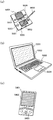
도 9b는 노트형 퍼스널 컴퓨터이며, 하우징(5201), 표시부(5202), 키보드(5203), 포인팅 디바이스(5204) 등을 갖는다. 본 발명의 일 형태에 따른 표시 장치는, 표시부(5202)에 사용할 수 있다. 표시부(5202)에 본 발명의 일 형태에 따른 표시 장치를 사용함으로써, 편리성이 우수한 3차원 화상 표시를 행할 수 있는 노트형 퍼스널 컴퓨터를 제공할 수 있다. 9B is a notebook personal computer, and has a
도 9c는 휴대 정보 단말이며, 하우징(5401), 표시부(5402), 조작키(5403) 등을 갖는다. 본 발명의 일 형태에 따른 표시 장치는, 표시부(5402)에 사용할 수 있다. 표시부(5402)에 본 발명의 일 형태에 따른 표시 장치를 사용함으로써, 편리성이 우수한 3차원 화상 표시를 행할 수 있는 휴대 정보 단말을 제공할 수 있다. 9C shows a portable information terminal, and has a
본 실시형태는, 다른 실시형태에 기재한 구성과 적절히 조합하여 실시할 수 있다. This embodiment can be implemented in appropriate combination with any of the structures described in the other embodiments.
본 실시예에서는, 제작한 본 발명의 일 형태의 3차원 표시 장치의 구성에 관해서 도 12를 사용하여 설명한다. 또한, 제작한 3차원 표시 장치로부터 30㎝의 거리에서 관측된 크로스토크의 평가 방법 및 평가 결과에 관해서 도 13a-L 내지 도 14를 사용하여 설명한다. In the present embodiment, the structure of the three-dimensional display device of one embodiment of the present invention produced will be described with reference to FIG. 12. In addition, the evaluation method and evaluation result of the crosstalk observed at a distance of 30 cm from the produced three-dimensional display apparatus are demonstrated using FIGS. 13A-L-14.
<구성><Configuration>
제작한 3차원 표시 장치 장치(1020)의 블록도를 도 12에 도시한다. 제작한 3차원 표시 장치 장치(1020)는, 표시 패널(1200)과, 시차 배리어를 형성하는 셔터 패널(1100)과, 초음파 센서(1160)와, 제어 장치(1030)를 갖는다. The block diagram of the produced three-
제작한 표시 패널(1200)은, 동일 기판 위에 구동 회로부(소스측 구동 회로, 게이트측 구동 회로)를 구비한 액티브 매트릭스형의 유기 EL 패널이다. 표시 패널(1200)은 대각이 3.9인치인 화소 영역을 구비하고, 이 화소 영역에는 수평 방향으로 1440개, 수직 방향으로 1080개의 복수의 화소가 매트릭스 형상으로 설치된다. 또한, 각각의 화소에는, 3개의 부화소가 설치된다. 또한 해상도는 458ppi가 된다.The produced
부화소의 크기는, 수평 방향을 55.5㎛, 수직 방향을 18.5㎛로 하였다. 개구율을 60%로 하였다. 또한, 3개의 부화소는 적색(R), 녹색(G), 적색(B)을 나타내는 빛을 발하는 구성으로 하고, 각 색을 가로 줄무늬 형상으로 배치했다. The size of the subpixel was 55.5 micrometers in the horizontal direction, and 18.5 micrometers in the vertical direction. The opening ratio was 60%. In addition, the three subpixels were configured to emit light indicating red (R), green (G), and red (B), and each color was arranged in a horizontal stripe shape.
제작한 셔터 패널(1100)은, 동일 기판 위에 구동 회로부를 구비하고, 전극마다 트랜지스터를 구비한 액티브 매트릭스형 셔터 패널이다. 셔터 패널(1100)은 대각이 3.9인치인 시차 배리어가 형성되는 영역을 구비하고, 그 영역에는 폭이 11.75㎛의 투광성을 갖는 전극이 세로 줄무늬 형상(vertical stripe pattern)으로 5760개가 설치된다. 또한, 인접하는 2개의 세로 줄무늬 형상의 전극 거리는, 시차 배리어가 형성되는 영역의 중앙에서 가장 좁게(구체적으로는 2㎛) 하고, 좌우의 단부에서 가장 넓게(구체적으로는 2.25㎛) 했다. 이와 같이 한 이유는, 관찰자가 3차원 표시 장치를 사용할 때, 상기 장치의 중앙에 바로 앞에 있는 상태에서 사용하는 빈도가 가장 높다고 생각했기 때문이다. The produced
표시 패널(1200)의 표시면측에 셔터 패널(1100)을 겹쳐서 설치했다. 또한, 표시 패널(1200)의 하나의 화소에 셔터 패널(1100)의 세로 줄무늬 형상의 전극 4개가 겹치도록 하였다. The
또한, 셔터 패널(1100)은, 네마틱(nematic) 액정층을 협지하는 세로 줄무늬 형상의 전극과 대향 전극을, 한 쌍의 편광판 사이에 갖는다. 상기 액정 소자를 입사광에 대해 불투과 되도록 구동함으로써, 시차 배리어를 형성했다. In addition, the
셔터 패널(1100)의 트랜지스터는 C축 배향을 갖는 결정성 산화물 반도체층을 구비한다. 구체적으로는, InGaZnO계의 산화물 반도체층을 구비한다. 채널 폭이 50㎛, 채널 길이가 6㎛인 트랜지스터는, 임계값 전압이 1.1V에서 노멀리 오프이며, 85℃에서의 오프 누설(off-state) 전류는, 채널 폭 1㎛당 100yA(10-22A)이었다. The transistor of the
제작한 트랜지스터에 조도 10klx의 환경하에서, 게이트 전위를 +20V의 상태에서 80℃, 1시간 유지하는 시험(+BT 시험), 및 게이트 전위를 -20V의 상태에서 1시간 유지하는 시험(-BT 시험)을 실시한 후의 트랜지스터의 특성을 도 16에 도시하였다. +BT 시험 후의 특성을 우측의 실선으로, -BT 시험 후의 특성을 좌측의 실선으로 도시하였다. 또한, 각각의 시험 전의 트랜지스터 특성은 2개의 실선 사이에 점선으로 도시하였다. A test for keeping the gate potential at 80 ° C. for 1 hour at +20 V in the environment of illuminance 10klx (+ BT test), and a test for keeping the gate potential at -20 V for 1 hour (-BT test) Fig. 16 shows the characteristics of the transistor after ()). The characteristic after + BT test is shown by the solid line on the right side, and the characteristic after -BT test is shown by the solid line on the left side. In addition, the transistor characteristics before each test are shown by the dotted line between two solid lines.
임계값 전압의 시프트 양은 -BT 시험 후에 -0.38V, +BT 시험 후에 +0.8V이었다. The shift amount of the threshold voltage was -0.38 V after the -BT test and +0.8 V after the + BT test.
관찰자의 위치를 검지하기 위하여, 초음파 센서(1160)를 사용했다. 초음파 센서(1160)는 20밀리 초의 시간 분해능과 0.5°의 각도 분해능을 구비한다. In order to detect the position of the observer, the
초음파 센서의 발진기가 발한 초음파를 대상이 반사하고, 초음파 센서의 검지기는 이 반사파를 수신하여, 대상의 위치를 검지한다. 초음파 센서가 수신하는 반사파의 일 예를 도 17a 내지 도 17c에 도시한다. The object reflects the ultrasonic wave emitted by the oscillator of the ultrasonic sensor, and the detector of the ultrasonic sensor receives the reflected wave and detects the position of the object. An example of the reflected wave received by the ultrasonic sensor is illustrated in FIGS. 17A to 17C.
대상이 초음파 센서 바로 앞에 있는 제 1 위치에 있을 때의 반사파의 검출 결과의 일 예를 도 17a에 도시한다. 좌우의 검지기는, 대략 같은 시간에, 같은 진폭의 반사파를 검출했다.An example of the detection result of the reflected wave when the object is in the first position immediately before the ultrasonic sensor is shown in FIG. 17A. The left and right detectors detected reflected waves of the same amplitude at approximately the same time.
다음에, 대상이 초음파 센서와의 거리를 바꾸지 않고 우측으로 치우친 제 2 위치에 있을 때의 반사파의 검출 결과의 일 예를 도 17b에 도시한다. 좌우의 검지기는, 대략 같은 시간에 반사파를 검출하지만, 우측의 검지기가 좌측의 검지기보다도 진폭이 큰 반사파를 검출하였다. Next, FIG. 17B shows an example of the detection result of the reflected wave when the object is in the second position to the right without changing the distance from the ultrasonic sensor. The left and right detectors detected reflected waves at about the same time, but the right detector detected reflected waves with a larger amplitude than the left detector.
다음에, 대상이 초음파 센서 바로 앞에 있고, 제 1 위치보다 먼 제 3 위치에 있을 때의 반사파의 검출 결과의 일 예를 도 17c에 도시한다. 좌우의 검지기는, 대략 같은 진폭의 반사파를 검출하지만, 대상이 제 1 위치에 있는 경우에 비해 지연되었다. Next, Fig. 17C shows an example of the detection result of the reflected wave when the object is directly in front of the ultrasonic sensor and at a third position far from the first position. The left and right detectors detect reflected waves of approximately the same amplitude, but are delayed compared to the case where the object is in the first position.
복수의 센서(Sensor)를 어레이 형상으로 설치하고, 각각의 센서에 증폭기(Amp)와 아날로그 디지털 변환기(ADC)와 지연 회로(Delay)를 직렬로 접속한 것을, 지연 적산 연산 회로(Delay Integration)에 병렬 접속하여, 지연 적산 연산을행하고, 대상의 위치(각도 및 거리)를 검출하였다(도 17d 참조).A plurality of sensors are provided in an array shape, and an amplifier, an analog-to-digital converter (ADC), and a delay circuit (Delay) are connected in series to each sensor in a delay integration circuit. In parallel connection, delay integration was performed, and the position (angle and distance) of the target was detected (see FIG. 17D).
<평가 방법><Evaluation method>
제작한 3차원 표시 장치로부터 30㎝의 거리에서, 발생하는 크로스토크의 정도를 평가하였다. 평가 방법을 이하에 설명한다. The degree of the crosstalk which generate | occur | produced at the distance of 30 cm from the produced three-dimensional display apparatus was evaluated. The evaluation method is described below.
평가에 사용한 화상을 도 13a-L 및 도 13a-R에 도시한다. 평가에는 오른쪽 눈용과 왼쪽 눈용의 2종류 화상을 사용하고, 모두 작은 정방형이 2개와 큰 정방형이 2개씩, 4개의 정방형이 그려져 있다. The image used for evaluation is shown to FIG. 13A-L and FIG. 13A-R. Two types of images, a right eye and a left eye, are used for evaluation, and four squares are drawn with two small squares and two large squares.
왼쪽 눈용의 화상과 오른쪽 눈용의 화상에는, 큰 정방형이 다른 배색으로 그려져 있다. 구체적으로는, 왼쪽 눈용의 화상(도 13a-L 참조)에는, 큰 흑색 정방형이 큰 백색 정방형의 좌측에 그려져 있고, 오른쪽 눈용의 화상(도 13a-R 참조)에는, 큰 흑색 정방형이 큰 백색 정방형의 우측에 그려져 있다. In the image for the left eye and the image for the right eye, a large square is drawn with a different color scheme. Specifically, a large black square is drawn on the left side of the large white square in the image for the left eye (see Figs. 13A-L), and a large black square is large on the left side of the image (see Figs. 13A-R) for the right eye. It is drawn on the right side of the.
그리고, 표시 패널(1200)의 왼쪽 눈용의 제 1 화소 영역에 왼쪽 눈용의 화상을 표시하고, 오른쪽 눈용의 제 2 화소 영역에 오른쪽 눈용의 화상을 표시하여 이하의 조건에서 관찰하였다. Then, the image for the left eye was displayed in the first pixel area for the left eye of the
제작한 3차원 표시 장치의 표시 패널(1200) 중앙으로부터 30㎝ 떨어져, 바로 앞에 있는 위치 및 바로 앞에 있는 위치로부터 우측 또는 좌측으로 14°까지, 2°마다 기울기가 다른 위치로부터 관찰하였다(도 13b 참조). 15개의 다른 조건에서 관찰한 결과를, 3D 디지털 영상 시스템(1300, 후지필름사제 FinePix 3D W3)을 사용하여 기록하였다. The inclination was observed every 2 degrees from the position in front of the
또한, 3D 디지털 영상 시스템(1300)은, 2개의 CCD 카메라를 좌우로 떨어진 위치에 구비하고, 각각의 카메라에서 왼쪽 눈이 포착한 영상과 오른쪽 눈이 포착한 영상을 독립하여 기록할 수 있다. In addition, the 3D
<평가 결과><Evaluation result>
제작한 3차원 표시 장치는, 50밀리 초마다 관찰자의 위치에 추종했다. 또한 각도 분해능은 2°였다. 제작한 3차원 표시 장치의 표시 결과를 도 14에 도시한다. 3차원 표시 장치 바로 앞에 있는 위치에서의 관측 결과를 최상단에, 바로 앞에 있는 위치로부터 우측 또는 좌측으로 14°까지, 2°마다 기울기가 다른 위치로부터의 관측 결과를 그 아래 나타냈다. The produced three-dimensional display device followed the observer's position every 50 milliseconds. In addition, the angular resolution was 2 degrees. The display result of the produced three-dimensional display device is shown in FIG. The observation result at the position immediately before the three-dimensional display device was shown at the top, and the observation result from the position where the inclination differs every 2 degrees from the immediately preceding position to 14 degrees to the right or left.
제작한 3차원 표시 장치는, 바로 앞에 있는 위치로부터 우측 또는 좌측으로 14°까지 비스듬한 위치에 있어도, 바로 앞에 있는 위치와 동일한 영상이 관찰되었다. 이러한 결과로부터, 특정한 관찰자가 나안으로 3차원 표시를 눈으로 확인할 수 있는 범위가 확대된 것이 나타났다. Even if the produced three-dimensional display device was in an oblique position from the position immediately before to 14 degrees to the right or left side, the same image as the position immediately before was observed. From these results, it was shown that the range where a particular observer could visually check the 3D display with naked eyes.
(비교예)(Comparative Example)
제작한 3차원 표시 장치를 사용하여, 바로 앞의 위치로부터의 관찰에 최적화된 시차 배리어를 형성했다. 시차 배리어의 형태를 그 상태로 고정하여, 30㎝의 거리에서 발생하는 크로스토크의 정도를, 비교예로서 평가했다. 즉, 본 비교예에서 예시하는 3차원 표시 장치는, 관찰 위치에 관계없이 형태가 일정한 시차 배리어를 갖는다. Using the produced three-dimensional display device, the parallax barrier optimized for observation from the position immediately before was formed. The form of the parallax barrier was fixed in that state, and the grade of the crosstalk which generate | occur | produces in the distance of 30 cm was evaluated as a comparative example. That is, the three-dimensional display device illustrated in this comparative example has a parallax barrier whose shape is constant regardless of the observation position.
본 비교예의 3차원 표시 장치의 표시 패널(1200)의 중앙으로부터 30㎝ 떨여저, 바로 앞에 있는 위치 및 바로 앞에 있는 위치로부터 우측 또는 좌측으로 14°까지, 2°마다 기울기가 다른 위치로부터, 제작한 3차원 표시 장치를 실시예에서 설명한 방법으로 평가했다. 30 cm away from the center of the
<비교예에 따른 장치의 평가 결과><Evaluation result of the device according to the comparative example>
비교예의 3차원 표시 장치의 표시 결과를 도 15에 도시한다. 3차원 표시 장치 바로 앞에 있는 위치에서의 관측 결과를 최상단에, 바로 앞에 있는 위치로부터 우측 또는 좌측으로 14°까지, 2°마다 기울기가 다른 위치로부터의 관측 결과를 그 아래에 나타냈다. The display result of the 3D display device of a comparative example is shown in FIG. The observation results at the position immediately before the three-dimensional display device are shown at the top, and the observation results from the positions with different inclinations every 2 degrees from the immediately preceding position to 14 degrees to the left or the left.
비교예의 3차원 표시 장치는, 바로 앞에 있는 위치로부터 우측 또는 좌측에 4°이상 비스듬한 위치로부터 크로스토크가 현저하게 되고, 8°이상 비스듬한 위치에서는, 오른쪽 눈용의 화상이 왼쪽 눈에서 관찰되고, 왼쪽 눈용의 화상이 오른쪽 눈에서 관찰되었다. 이러한 결과로부터, 형태가 고정된 시차 배리어를 갖는 3차원 표시 장치는 관찰자가 나안으로 3차원 표시를 눈으로 확인할 수 있는 범위가 좁은 것이 나타났다. In the three-dimensional display device of the comparative example, crosstalk is remarkable from a position at an angle of 4 ° or more to the right or left from the position immediately in front, and at a position at an angle of 8 ° or more, an image for the right eye is observed in the left eye, and for the left eye. Burns were observed in the right eye. From these results, it has been shown that a three-dimensional display device having a fixed parallax barrier has a narrow range in which an observer can visually check a three-dimensional display with naked eyes.
10; 관찰자 10L; 왼쪽 눈
10R; 오른쪽 눈 20; 표시 장치
30; 제어 장치 90; 시차 배리어
100; 셔터 패널 101; 기판
102; 기판 103; 액정층
105; 전극 105a; 전극
105b; 전극 105c; 전극
105b1; 전극 106; 전극
106a; 전극 106a1~3; 전극
106b; 전극 106b1~5; 전극
106c1~3; 전극 107a1~3; 액정 소자
107b1~3; 액정 소자 107c1~3; 액정 소자
116a; 전극 116a1~3; 전극
120a1~3; 트랜지스터 121a; 배선
122a1~3; 배선 124; 용량 배선
150; 시차 배리어 제어 회로 160; 관찰자 검지 회로
161; 초음파 발진기 162L; 검지기
162R; 검지기 200; 표시 패널
210; 화소 영역 220; 화소 영역
250; 표시 패널 구동 회로 260; 화상 신호 생성 회로
401; 소스측 구동 회로 402; 화소부
403; 게이트측 구동 회로 404; 밀봉 기판
405; 씰재 407; 공간
408; 배선 409; FPC(플렉시블 프린트 서킷)
410; 소자 기판 411; 절연막
412a; 트랜지스터 412b; 트랜지스터
412c; 트랜지스터 413a; 전극
413b; 전극 413c; 전극
414; 절연물 415a; 도전층
415b; 도전층 415c; 도전층
418a; 발광 소자 418b; 발광 소자
418c; 발광 소자 419; 절연막
420a; 화소 420b; 화소
420c; 화소 423; n-채널형 트랜지스터
424; p-채널형 트랜지스터 431; EL층
433; 전극 434a; 컬러 필터층
434b; 컬러 필터층 434c; 컬러 필터층
601; 기판 602; 화소부
603; 신호선 구동 회로 604; 주사선 구동 회로
605; 씰재 606; 기판
608; 액정층 610; 트랜지스터
611; 트랜지스터 613; 액정 소자
615; 접속 단자 전극 616; 단자 전극
618; FPC 619; 이방성 도전막
630; 전극층 631; 전극층
632; 절연막 633; 절연막
635; 스페이서 640; 셔터 패널
642; 편광판 644; 기판
646; 기판 648; 편광판
650; 액정 소자 유닛 652; 기판
660; 터치 패널 유닛 661; 도전막
662; 전극 663; 도전막
664; 전극 666; 절연층
668; 절연층 690; 시차 배리어
700; 표시 패널 710; 화소 영역
720; 화소 영역 1020; 표시 장치
1030; 제어 장치 1100; 셔터 패널
1160; 초음파 센서 1200; 표시 패널
1300; 3D 디지털 영상 시스템 5001; 하우징
5002; 하우징 5003; 표시부
5004; 표시부 5005; 마이크로폰
5006; 스피커 5007; 조작키
5008; 스타일러스 5201; 하우징
5202; 표시부 5203; 키보드
5204; 포인팅 디바이스 5401; 하우징
5402; 표시부 5403; 조작키10;
10R;
30;
100;
102;
105;
105b;
105b1;
106a; Electrodes 106a1 to 3; electrode
106b; Electrodes 106b1 to 5; electrode
106c1-3; Electrodes 107a1 to 3; Liquid crystal element
107b1-3; Liquid crystal elements 107c1 to 3; Liquid crystal element
116a; Electrodes 116a1 to 3; electrode
120a1-3;
122a1-3;
150; Parallax
161;
162R;
210; The
250; Display
401; Source
403; Gate
405;
408;
410;
412a; Transistor 412b; transistor
412c; Transistor 413a; electrode
413b; Electrode 413c; electrode
414;
415b;
418a;
418c;
420a;
420c;
424; p-
433;
434b;
601;
603; Signal
605;
608;
611;
615;
618;
630;
632; Insulating
635;
642;
646;
650; A liquid
660;
662;
664;
668; Insulating
700;
720;
1030;
1160;
1300; 3D
5002;
5004;
5006;
5008;
5202;
5204;
5402;
Claims (16)
상기 표시 패널의 일부를 차단하고 형태가 변하는 시차 배리어(parallax barrier);
상기 시차 배리어의 형태를 제어하도록 구성된 시차 배리어 제어 회로;
초음파 발진기; 및
관찰자로부터 반사된 초음파를 검지하도록 구성된 복수의 검지기들을 포함하고,
상기 시차 배리어 제어 회로는 상기 복수의 검지기들에 의해 특정된 상기 관찰자의 위치에 따라 상기 시차 배리어를 제어하여 상기 시차 배리어가 상기 관찰자의 오른쪽 눈이 상기 제 1 화소 영역을 보는 것을 차단하고 상기 관찰자의 왼쪽 눈이 상기 제 2 화소 영역을 보는 것을 차단하게 하는, 표시 장치.A display panel including a first pixel area for a left eye and a second pixel area for a right eye;
A parallax barrier blocking a portion of the display panel and changing in shape;
A parallax barrier control circuit configured to control a shape of the parallax barrier;
Ultrasonic oscillator; And
A plurality of detectors configured to detect ultrasonic waves reflected from an observer,
The parallax barrier control circuit controls the parallax barrier according to the position of the observer specified by the plurality of detectors so that the parallax barrier blocks the right eye of the observer from seeing the first pixel area and And a left eye to block viewing of the second pixel area.
상기 시차 배리어는 한 쌍의 기판들 사이에 개재된 액정층을 포함하고,
상기 한 쌍의 기판들 중 적어도 하나에는 상기 액정층의 액정들의 배향을 제어하기 위한 복수의 전극들이 제공되고, 상기 복수의 전극들 각각은 상기 시차 배리어 제어 회로에 전기적으로 접속되는, 표시 장치.The method of claim 1,
The parallax barrier includes a liquid crystal layer interposed between the pair of substrates,
At least one of the pair of substrates is provided with a plurality of electrodes for controlling the orientation of liquid crystals of the liquid crystal layer, each of the plurality of electrodes being electrically connected to the parallax barrier control circuit.
상기 시차 배리어의 형태는 스트라이프 형상, 체크무늬 형상, 십자 형상(crossed pattern)인, 표시 장치.The method of claim 1,
The parallax barrier may have a stripe shape, a checkered shape, and a crossed pattern.
상기 표시 패널에 제공된 표시 소자는 유기 EL(electroluminescent) 소자인, 표시 장치.The method of claim 1,
A display device provided in the display panel is an organic electroluminescent (EL) device.
상기 표시 패널에 제공된 표시 소자는 액정 소자인, 표시 장치.The method of claim 1,
The display device provided in the said display panel is a liquid crystal element.
시차 배리어를 포함하는 셔터 패널;
제어 장치;
초음파 발진기; 및
관찰자로부터 반사된 초음파를 검지하도록 구성된 복수의 검지기들을 포함하고,
상기 표시 패널, 상기 셔터 패널, 상기 초음파 발진기, 및 상기 복수의 검지기들은 상기 제어 장치에 접속되고,
상기 제어 장치는 상기 복수의 검지기들에 의해 특정된 상기 관찰자의 위치에 따라 상기 시차 배리어의 형태를 변경하도록 상기 셔터 패널을 제어하는, 표시 장치.Display panel;
A shutter panel comprising a parallax barrier;
controller;
Ultrasonic oscillator; And
A plurality of detectors configured to detect ultrasonic waves reflected from an observer,
The display panel, the shutter panel, the ultrasonic oscillator, and the plurality of detectors are connected to the control device,
And the control device controls the shutter panel to change the shape of the parallax barrier in accordance with the position of the observer specified by the plurality of detectors.
상기 셔터 패널은 한 쌍의 기판들 사이에 개재된 액정층을 포함하고,
상기 한 쌍의 기판들 중 적어도 하나에는 상기 액정층의 액정들의 배향을 제어하기 위한 복수의 전극들이 제공되고, 상기 복수의 전극들 각각은 상기 제어 장치에 전기적으로 접속되는, 표시 장치.The method according to claim 6,
The shutter panel includes a liquid crystal layer interposed between a pair of substrates,
At least one of the pair of substrates is provided with a plurality of electrodes for controlling the orientation of the liquid crystals of the liquid crystal layer, each of the plurality of electrodes being electrically connected to the control device.
서로 인접한 두 전극들 간의 거리는 상기 표시 패널의 중앙에서 가장 작고,
상기 서로 인접한 두 전극들 간의 거리는 상기 표시 패널의 좌우 단부에서 가장 큰, 표시 장치.The method of claim 7, wherein
The distance between two adjacent electrodes is the smallest in the center of the display panel,
And a distance between the two adjacent electrodes is largest at left and right ends of the display panel.
상기 시차 배리어의 형태는 스트라이프 형상, 체크무늬 형상, 십자 형상인, 표시 장치.The method according to claim 6,
The form of the parallax barrier is a stripe shape, a checkered shape, a cross shape.
상기 셔터 패널은 복수의 트랜지스터들을 포함하는 액티브 매트릭스 셔터 패널인, 표시 장치.The method according to claim 6,
And the shutter panel is an active matrix shutter panel including a plurality of transistors.
상기 복수의 트랜지스터들은 산화물 반도체를 포함하는, 표시 장치.11. The method of claim 10,
And the plurality of transistors comprise an oxide semiconductor.
상기 표시 패널에 제공된 표시 소자는 유기 EL 소자인, 표시 장치.The method according to claim 6,
A display device provided in the display panel is an organic EL device.
상기 표시 패널에 제공된 표시 소자는 액정 소자인, 표시 장치.The method according to claim 6,
The display device provided in the said display panel is a liquid crystal element.
상기 표시 장치의 표시면이 관찰자와 마주하는 측의 앞 공간으로 펄스형(pulsed)의 초음파를 발신하는 단계;
반사된 펄스형의 초음파가 복수의 검지기들 각각에 의해 검지되는데 걸리는 시간에 기초하여 상기 관찰자의 위치를 특정하는 단계;
상기 관찰자의 위치를 통과하는 직선이 표시면과 수직으로 교차하는 좌표를 산출하여, 상기 관찰자의 정면과 마주하는 한 쌍의 오른쪽 눈용 및 왼쪽 눈용의 화소들을 특정하는 단계;
상기 한 쌍의 오른쪽 눈용 및 왼쪽 눈용의 화소들로부터 상기 관찰자까지의 거리를 특정하는 단계;
상기 관찰자의 오른쪽 눈이 상기 오른쪽 눈용의 화소를, 상기 관찰자의 왼쪽 눈이 상기 왼쪽 눈용의 화소를 관찰할 수 있도록, 상기 한 쌍의 오른쪽 눈용 및 왼쪽 눈용의 화소들에 대응하는 시차 배리어의 크기를 상기 한 쌍의 오른쪽 눈용 및 왼쪽 눈용의 화소들로부터 상기 관찰자까지의 거리를 참조하여 제어하는 단계; 및
다른 쌍의 오른쪽 눈용 및 왼쪽 눈용의 화소들을 아랫변으로 하고 상기 시차 배리어의 차광부를 윗변으로 하는 사다리꼴이 상기 관찰자측으로 기울어지고(fall toward the viewer), 상기 사다리꼴이 관찰자의 정면과 마주하는 화소들로부터 수평 방향으로 더 멀어질수록 더 왜곡되도록 상기 시차 배리어를 형성하는 단계로서, 상기 시차 배리어가 상기 관찰자의 왼쪽 눈이 상기 오른쪽 눈용 화소 영역을 보는 것을 차단하고 상기 관찰자의 오른쪽 눈이 상기 왼쪽 눈용 화소 영역을 보는 것을 차단하도록 하는, 상기 시차 배리어 형성 단계를 포함하는, 표시 장치 구동 방법.In a method of driving a display device:
Transmitting a pulsed ultrasonic wave to a space in front of the side of the display device facing the observer;
Specifying the position of the observer based on the time taken for the reflected pulsed ultrasonic wave to be detected by each of the plurality of detectors;
Calculating coordinates in which a straight line passing through the viewer's position perpendicularly intersects a display surface, and specifies a pair of pixels for right and left eyes facing the front of the observer;
Specifying a distance from the pair of right eye and left eye pixels to the viewer;
The size of the parallax barrier corresponding to the pair of right eye and left eye pixels so that the observer's right eye can observe the pixels for the right eye and the observer's left eye can observe the pixels for the left eye. Controlling the distance from the pair of right eye and left eye pixels to the viewer; And
A trapezoid with the other pair of right eye and left eye pixels as the lower side and the light shielding portion of the parallax barrier as the upper side falls toward the viewer, and the trapezoid from the pixels facing the front of the viewer. Forming the parallax barrier so as to be distorted further in a horizontal direction, wherein the parallax barrier blocks the observer's left eye from viewing the right eye pixel area and the observer's right eye from the left eye pixel area And forming a parallax barrier to block viewing of the light source.
상기 표시 장치의 표시면이 관찰자와 마주하는 측의 앞 공간으로 펄스형의 초음파를 발신하는 단계;
반사된 펄스형의 초음파가 복수의 검지기들 각각에 의해 검지되는데 걸리는 시간에 기초하여 상기 관찰자의 위치를 특정하는 단계;
상기 관찰자의 위치에 기초하여 상기 관찰자의 정면과 마주하는 한 쌍의 오른쪽 눈용 및 왼쪽 눈용의 화소들을 특정하는 단계;
상기 한 쌍의 오른쪽 눈용 및 왼쪽 눈용의 화소들로부터 상기 관찰자까지의 거리를 특정하는 단계;
상기 관찰자의 오른쪽 눈이 상기 오른쪽 눈용의 화소를, 상기 관찰자의 왼쪽 눈이 상기 왼쪽 눈용의 화소를 관찰할 수 있도록, 상기 한 쌍의 오른쪽 눈용 및 왼쪽 눈용의 화소들에 대응하는 시차 배리어의 크기를 상기 한 쌍의 오른쪽 눈용 및 왼쪽 눈용의 화소들로부터 상기 관찰자까지의 거리를 참조하여 제어하는 단계; 및
다른 쌍의 오른쪽 눈용 및 왼쪽 눈용의 화소들을 아랫변으로 하고 상기 시차 배리어의 차광부를 윗변으로 하는 사다리꼴이 상기 관찰자측으로 기울어지고, 상기 사다리꼴이 관찰자의 정면과 마주하는 화소들로부터 수평 방향으로 더 멀어질수록 더 왜곡되도록 상기 시차 배리어를 형성하는 단계로서, 상기 시차 배리어가 상기 관찰자의 왼쪽 눈이 상기 오른쪽 눈용 화소 영역을 보는 것을 차단하고 상기 관찰자의 오른쪽 눈이 상기 왼쪽 눈용 화소 영역을 보는 것을 차단하도록 하는, 상기 시차 배리어 형성 단계를 포함하는, 표시 장치 구동 방법.In a method of driving a display device:
Transmitting a pulsed ultrasonic wave to a space in front of a side of the display device facing the observer;
Specifying the position of the observer based on the time taken for the reflected pulsed ultrasonic wave to be detected by each of the plurality of detectors;
Specifying a pair of pixels for the right eye and the left eye facing the front of the observer based on the position of the observer;
Specifying a distance from the pair of right eye and left eye pixels to the viewer;
The size of the parallax barrier corresponding to the pair of right eye and left eye pixels so that the observer's right eye can observe the pixels for the right eye and the observer's left eye can observe the pixels for the left eye. Controlling the distance from the pair of right eye and left eye pixels to the viewer; And
A trapezoid with the other pair of right eye and left eye pixels as the lower side and the light shielding portion of the parallax barrier as the upper side will be inclined toward the observer side, and the trapezoid will be further horizontally away from the pixels facing the front of the observer. Forming the parallax barrier such that the parallax barrier is further distorted so that the parallax barrier blocks the observer's left eye from viewing the right eye pixel area and the observer's right eye from viewing the left eye pixel area. And forming the parallax barrier.
상기 표시 장치의 표시면이 관찰자와 마주하는 측의 앞 공간으로 펄스형의 초음파를 발신하는 단계;
반사된 펄스형의 초음파가 복수의 검지기들 각각에 의해 검지되는데 걸리는 시간 및 상기 복수의 검지기들 각각에 의해 검지되는 상기 반사된 펄스형의 초음파의 진폭에 기초하여 상기 관찰자의 위치를 특정하는 단계; 및
상기 관찰자의 위치에 따라 시차 배리어를 형성하는 단계를 포함하는, 표시 장치 구동 방법.In a method of driving a display device:
Transmitting a pulsed ultrasonic wave to a space in front of a side of the display device facing the observer;
Specifying the position of the observer based on the time it takes for the reflected pulsed ultrasound to be detected by each of the plurality of detectors and the amplitude of the reflected pulsed ultrasound detected by each of the plurality of detectors; And
And forming a parallax barrier according to the position of the observer.
Applications Claiming Priority (4)
| Application Number | Priority Date | Filing Date | Title |
|---|---|---|---|
| JP2011054824 | 2011-03-11 | ||
| JPJP-P-2011-054824 | 2011-03-11 | ||
| JPJP-P-2011-259801 | 2011-11-29 | ||
| JP2011259801 | 2011-11-29 |
Publications (1)
| Publication Number | Publication Date |
|---|---|
| KR20120104105A true KR20120104105A (en) | 2012-09-20 |
Family
ID=46795093
Family Applications (1)
| Application Number | Title | Priority Date | Filing Date |
|---|---|---|---|
| KR1020120024330A KR20120104105A (en) | 2011-03-11 | 2012-03-09 | Display device and method for driving the same |
Country Status (5)
| Country | Link |
|---|---|
| US (2) | US9558687B2 (en) |
| JP (1) | JP5912680B2 (en) |
| KR (1) | KR20120104105A (en) |
| CN (1) | CN102682688B (en) |
| TW (1) | TWI554786B (en) |
Cited By (1)
| Publication number | Priority date | Publication date | Assignee | Title |
|---|---|---|---|---|
| CN106291956A (en) * | 2016-08-26 | 2017-01-04 | 京东方科技集团股份有限公司 | Display panel assembly and preparation method thereof and display device |
Families Citing this family (30)
| Publication number | Priority date | Publication date | Assignee | Title |
|---|---|---|---|---|
| KR20130010834A (en) | 2011-07-19 | 2013-01-29 | 가부시키가이샤 한도오따이 에네루기 켄큐쇼 | Display device |
| TWI448939B (en) * | 2011-12-06 | 2014-08-11 | Shih Hua Technology Ltd | Touch panel |
| CN102798982B (en) | 2012-08-31 | 2015-11-25 | 深圳超多维光电子有限公司 | A kind of stereoscopic display device and stereo display control method |
| KR101964066B1 (en) * | 2012-10-02 | 2019-04-02 | 삼성디스플레이 주식회사 | Display apparatus and method of displaying three dimensional image using the same |
| KR20140054532A (en) * | 2012-10-29 | 2014-05-09 | 삼성디스플레이 주식회사 | Method of driving active barrier panel and display apparatus for performing the method |
| US10116911B2 (en) * | 2012-12-18 | 2018-10-30 | Qualcomm Incorporated | Realistic point of view video method and apparatus |
| KR101996655B1 (en) * | 2012-12-26 | 2019-07-05 | 엘지디스플레이 주식회사 | apparatus for displaying a hologram |
| KR20140090482A (en) * | 2013-01-09 | 2014-07-17 | 삼성디스플레이 주식회사 | Display device |
| US10222911B2 (en) | 2013-04-12 | 2019-03-05 | Semiconductor Energy Laboratory Co., Ltd. | Semiconductor device and driving method of the same |
| CN103424924B (en) * | 2013-08-09 | 2015-12-09 | 京东方科技集团股份有限公司 | The display device of changeable two dimension and three-dimensional display mode |
| US10116914B2 (en) * | 2013-10-31 | 2018-10-30 | 3Di Llc | Stereoscopic display |
| US10565925B2 (en) | 2014-02-07 | 2020-02-18 | Samsung Electronics Co., Ltd. | Full color display with intrinsic transparency |
| US10375365B2 (en) | 2014-02-07 | 2019-08-06 | Samsung Electronics Co., Ltd. | Projection system with enhanced color and contrast |
| US10453371B2 (en) | 2014-02-07 | 2019-10-22 | Samsung Electronics Co., Ltd. | Multi-layer display with color and contrast enhancement |
| US10554962B2 (en) * | 2014-02-07 | 2020-02-04 | Samsung Electronics Co., Ltd. | Multi-layer high transparency display for light field generation |
| DE202014010466U1 (en) * | 2014-04-30 | 2015-08-20 | Ernst-Abbe-Hochschule Jena | Apparatus for the simultaneous generation of stereoscopic images |
| JP2016040569A (en) * | 2014-08-12 | 2016-03-24 | 大日本印刷株式会社 | Stereoscopic vision display device, liquid crystal lens cell with low reflection layer, and sensor substrate with low reflection layer |
| US11468639B2 (en) * | 2015-02-20 | 2022-10-11 | Microsoft Technology Licensing, Llc | Selective occlusion system for augmented reality devices |
| CN105681778B (en) * | 2016-01-05 | 2018-07-10 | 京东方科技集团股份有限公司 | A kind of three-dimensional display apparatus and its driving method |
| CN109691096A (en) * | 2016-09-23 | 2019-04-26 | 夏普株式会社 | The control method of display device and display device |
| CN109937443A (en) * | 2016-11-10 | 2019-06-25 | 株式会社半导体能源研究所 | The driving method of display device and display device |
| CN108074267B (en) | 2016-11-18 | 2023-08-11 | 松下知识产权经营株式会社 | Intersection point detection device and method, camera correction system and method, and recording medium |
| JP7075358B2 (en) * | 2017-01-26 | 2022-05-25 | 株式会社半導体エネルギー研究所 | Semiconductor devices and electronic devices |
| WO2018138603A1 (en) | 2017-01-26 | 2018-08-02 | Semiconductor Energy Laboratory Co., Ltd. | Semiconductor device and electronic device including the semiconductor device |
| WO2018142610A1 (en) * | 2017-02-06 | 2018-08-09 | 三菱電機株式会社 | Stereoscopic display device and head-up display |
| JP6981760B2 (en) * | 2017-03-10 | 2021-12-17 | 株式会社半導体エネルギー研究所 | Semiconductor device |
| CN108877606A (en) * | 2017-05-09 | 2018-11-23 | 京东方科技集团股份有限公司 | Control method, the control system of display screen of display screen |
| TWI632540B (en) * | 2018-01-15 | 2018-08-11 | 友達光電股份有限公司 | Display apparatus and method of switching viewing angle thereof |
| CN108469682A (en) * | 2018-03-30 | 2018-08-31 | 京东方科技集团股份有限公司 | A kind of three-dimensional display apparatus and its 3 D displaying method |
| JP6924903B2 (en) * | 2018-06-26 | 2021-08-25 | 京セラ株式会社 | Information display device and information display system |
Family Cites Families (27)
| Publication number | Priority date | Publication date | Assignee | Title |
|---|---|---|---|---|
| JPH05122733A (en) | 1991-10-28 | 1993-05-18 | Nippon Hoso Kyokai <Nhk> | Three-dimensional picture display device |
| GB2296617A (en) | 1994-12-29 | 1996-07-03 | Sharp Kk | Observer tracking autosteroscopic display |
| JPH0980354A (en) | 1995-09-12 | 1997-03-28 | Toshiba Corp | Stereoscopic video device |
| GB2317710A (en) | 1996-09-27 | 1998-04-01 | Sharp Kk | Spatial light modulator and directional display |
| JPH10174127A (en) * | 1996-12-13 | 1998-06-26 | Sanyo Electric Co Ltd | Method and device for three-dimensional display |
| JPH10232626A (en) | 1997-02-20 | 1998-09-02 | Canon Inc | Stereoscopic image display device |
| JP4068188B2 (en) | 1997-09-02 | 2008-03-26 | 富士通株式会社 | Image display device |
| JPH11285030A (en) | 1998-03-26 | 1999-10-15 | Mr System Kenkyusho:Kk | Stereoscopic image display method and stereoscopic image display device |
| JP4515259B2 (en) | 2002-10-30 | 2010-07-28 | 株式会社半導体エネルギー研究所 | Display device and electronic device |
| JP2005164916A (en) * | 2003-12-02 | 2005-06-23 | Canon Inc | Stereoscopic display device |
| JP2005258013A (en) | 2004-03-11 | 2005-09-22 | Sharp Corp | Display panel and display device |
| US20050212984A1 (en) * | 2004-03-26 | 2005-09-29 | Yi-Chun Wu | Dual-mode display system for 2D and 3D viewing |
| GB2418315A (en) | 2004-09-21 | 2006-03-22 | Sharp Kk | Multiple view display |
| US20060139448A1 (en) * | 2004-12-29 | 2006-06-29 | Samsung Electronics Co., Ltd. | 3D displays with flexible switching capability of 2D/3D viewing modes |
| KR101249988B1 (en) * | 2006-01-27 | 2013-04-01 | 삼성전자주식회사 | Apparatus and method for displaying image according to the position of user |
| JP5006587B2 (en) * | 2006-07-05 | 2012-08-22 | 株式会社エヌ・ティ・ティ・ドコモ | Image presenting apparatus and image presenting method |
| KR20080060950A (en) | 2006-12-27 | 2008-07-02 | 엘지디스플레이 주식회사 | Three dimensional image display device and driving method thereof |
| WO2009095862A1 (en) | 2008-02-01 | 2009-08-06 | Koninklijke Philips Electronics N.V. | Autostereoscopic display device |
| GB2457691A (en) | 2008-02-21 | 2009-08-26 | Sharp Kk | Display with regions simultaneously operable in different viewing modes |
| TW201035966A (en) | 2009-03-17 | 2010-10-01 | Chunghwa Picture Tubes Ltd | Method of observing a depth fused display |
| JP4719929B2 (en) * | 2009-03-31 | 2011-07-06 | Necカシオモバイルコミュニケーションズ株式会社 | Display device and program |
| JP4525831B1 (en) * | 2009-03-31 | 2010-08-18 | 株式会社カシオ日立モバイルコミュニケーションズ | Image receiving apparatus and program |
| TW201040581A (en) * | 2009-05-06 | 2010-11-16 | J Touch Corp | Digital image capturing device with stereo image display and touch functions |
| JP5366137B2 (en) | 2009-05-28 | 2013-12-11 | 独立行政法人情報通信研究機構 | Video display system and video display method |
| JP5356952B2 (en) * | 2009-08-31 | 2013-12-04 | レムセン イノベーション、リミティッド ライアビリティー カンパニー | Display device |
| US8964013B2 (en) | 2009-12-31 | 2015-02-24 | Broadcom Corporation | Display with elastic light manipulator |
| CN101923257B (en) | 2010-08-06 | 2011-12-14 | 友达光电股份有限公司 | Parallax control element, display device and formation method of automatic stereoscopic image |
-
2012
- 2012-03-07 JP JP2012050420A patent/JP5912680B2/en not_active Expired - Fee Related
- 2012-03-07 US US13/413,703 patent/US9558687B2/en active Active
- 2012-03-09 KR KR1020120024330A patent/KR20120104105A/en not_active Application Discontinuation
- 2012-03-09 TW TW101108127A patent/TWI554786B/en not_active IP Right Cessation
- 2012-03-09 CN CN201210060735.4A patent/CN102682688B/en not_active Expired - Fee Related
-
2016
- 2016-12-22 US US15/388,003 patent/US10218967B2/en active Active
Cited By (1)
| Publication number | Priority date | Publication date | Assignee | Title |
|---|---|---|---|---|
| CN106291956A (en) * | 2016-08-26 | 2017-01-04 | 京东方科技集团股份有限公司 | Display panel assembly and preparation method thereof and display device |
Also Published As
| Publication number | Publication date |
|---|---|
| CN102682688A (en) | 2012-09-19 |
| US10218967B2 (en) | 2019-02-26 |
| TW201300840A (en) | 2013-01-01 |
| JP2013137486A (en) | 2013-07-11 |
| CN102682688B (en) | 2016-05-11 |
| US9558687B2 (en) | 2017-01-31 |
| US20120229431A1 (en) | 2012-09-13 |
| JP5912680B2 (en) | 2016-04-27 |
| US20170104985A1 (en) | 2017-04-13 |
| TWI554786B (en) | 2016-10-21 |
Similar Documents
| Publication | Publication Date | Title |
|---|---|---|
| KR20120104105A (en) | Display device and method for driving the same | |
| JP6181788B2 (en) | Liquid crystal display device, display module, and electronic device | |
| JP6295293B2 (en) | Display device | |
| KR102503847B1 (en) | Display device | |
| US10817105B2 (en) | Liquid crystal display device | |
| CN102830559B (en) | Display device | |
| US9097947B2 (en) | Display device and manufacturing method thereof | |
| JP2012190017A (en) | Display device | |
| US9451246B2 (en) | Display device | |
| JPWO2013179537A1 (en) | Liquid crystal display | |
| CN104105999B (en) | three-dimensional display device | |
| CN103529587A (en) | Patterned retarder type stereoscopic image display device and method for manufacturing the same | |
| TWI603252B (en) | Liquid crystal display device |
Legal Events
| Date | Code | Title | Description |
|---|---|---|---|
| A201 | Request for examination | ||
| E902 | Notification of reason for refusal | ||
| E601 | Decision to refuse application |