KR20120101357A - Light signal transmitter and light receiver for an optical sensor - Google Patents
Light signal transmitter and light receiver for an optical sensor Download PDFInfo
- Publication number
- KR20120101357A KR20120101357A KR1020127010615A KR20127010615A KR20120101357A KR 20120101357 A KR20120101357 A KR 20120101357A KR 1020127010615 A KR1020127010615 A KR 1020127010615A KR 20127010615 A KR20127010615 A KR 20127010615A KR 20120101357 A KR20120101357 A KR 20120101357A
- Authority
- KR
- South Korea
- Prior art keywords
- optical
- printed circuit
- circuit board
- light source
- semiconductor based
- Prior art date
Links
Images
Classifications
-
- G—PHYSICS
- G01—MEASURING; TESTING
- G01V—GEOPHYSICS; GRAVITATIONAL MEASUREMENTS; DETECTING MASSES OR OBJECTS; TAGS
- G01V8/00—Prospecting or detecting by optical means
- G01V8/02—Prospecting
-
- G—PHYSICS
- G01—MEASURING; TESTING
- G01V—GEOPHYSICS; GRAVITATIONAL MEASUREMENTS; DETECTING MASSES OR OBJECTS; TAGS
- G01V8/00—Prospecting or detecting by optical means
- G01V8/10—Detecting, e.g. by using light barriers
-
- G—PHYSICS
- G01—MEASURING; TESTING
- G01V—GEOPHYSICS; GRAVITATIONAL MEASUREMENTS; DETECTING MASSES OR OBJECTS; TAGS
- G01V8/00—Prospecting or detecting by optical means
- G01V8/10—Detecting, e.g. by using light barriers
- G01V8/12—Detecting, e.g. by using light barriers using one transmitter and one receiver
-
- H—ELECTRICITY
- H05—ELECTRIC TECHNIQUES NOT OTHERWISE PROVIDED FOR
- H05K—PRINTED CIRCUITS; CASINGS OR CONSTRUCTIONAL DETAILS OF ELECTRIC APPARATUS; MANUFACTURE OF ASSEMBLAGES OF ELECTRICAL COMPONENTS
- H05K3/00—Apparatus or processes for manufacturing printed circuits
- H05K3/46—Manufacturing multilayer circuits
- H05K3/4697—Manufacturing multilayer circuits having cavities, e.g. for mounting components
-
- H—ELECTRICITY
- H05—ELECTRIC TECHNIQUES NOT OTHERWISE PROVIDED FOR
- H05K—PRINTED CIRCUITS; CASINGS OR CONSTRUCTIONAL DETAILS OF ELECTRIC APPARATUS; MANUFACTURE OF ASSEMBLAGES OF ELECTRICAL COMPONENTS
- H05K1/00—Printed circuits
- H05K1/02—Details
- H05K1/0274—Optical details, e.g. printed circuits comprising integral optical means
-
- H—ELECTRICITY
- H05—ELECTRIC TECHNIQUES NOT OTHERWISE PROVIDED FOR
- H05K—PRINTED CIRCUITS; CASINGS OR CONSTRUCTIONAL DETAILS OF ELECTRIC APPARATUS; MANUFACTURE OF ASSEMBLAGES OF ELECTRICAL COMPONENTS
- H05K1/00—Printed circuits
- H05K1/02—Details
- H05K1/14—Structural association of two or more printed circuits
- H05K1/144—Stacked arrangements of planar printed circuit boards
-
- H—ELECTRICITY
- H05—ELECTRIC TECHNIQUES NOT OTHERWISE PROVIDED FOR
- H05K—PRINTED CIRCUITS; CASINGS OR CONSTRUCTIONAL DETAILS OF ELECTRIC APPARATUS; MANUFACTURE OF ASSEMBLAGES OF ELECTRICAL COMPONENTS
- H05K2201/00—Indexing scheme relating to printed circuits covered by H05K1/00
- H05K2201/04—Assemblies of printed circuits
- H05K2201/042—Stacked spaced PCBs; Planar parts of folded flexible circuits having mounted components in between or spaced from each other
-
- H—ELECTRICITY
- H05—ELECTRIC TECHNIQUES NOT OTHERWISE PROVIDED FOR
- H05K—PRINTED CIRCUITS; CASINGS OR CONSTRUCTIONAL DETAILS OF ELECTRIC APPARATUS; MANUFACTURE OF ASSEMBLAGES OF ELECTRICAL COMPONENTS
- H05K2201/00—Indexing scheme relating to printed circuits covered by H05K1/00
- H05K2201/10—Details of components or other objects attached to or integrated in a printed circuit board
- H05K2201/10007—Types of components
- H05K2201/10106—Light emitting diode [LED]
-
- H—ELECTRICITY
- H05—ELECTRIC TECHNIQUES NOT OTHERWISE PROVIDED FOR
- H05K—PRINTED CIRCUITS; CASINGS OR CONSTRUCTIONAL DETAILS OF ELECTRIC APPARATUS; MANUFACTURE OF ASSEMBLAGES OF ELECTRICAL COMPONENTS
- H05K2201/00—Indexing scheme relating to printed circuits covered by H05K1/00
- H05K2201/20—Details of printed circuits not provided for in H05K2201/01 - H05K2201/10
- H05K2201/2054—Light-reflecting surface, e.g. conductors, substrates, coatings, dielectrics
Abstract
FIELD OF THE INVENTION The present invention relates to optical sensors, in particular optical signal transmitters and optical receivers for industrial automation systems, wherein the optical signal transmitter comprises a semiconductor based light source (LD) for generating light, the semiconductor based light source (LD) having multiple layers. Disposed in an installation space between the outer layers OL and UL of the rotatable substrate LP, and the light emission direction of the semiconductor-based light source LD is oriented substantially parallel to the layers LAY of the printed circuit board LP And a refracting unit UE for refracting the light emitted by the semiconductor-based light source LD in a direction substantially perpendicular to the layer LAY of the printed circuit board LP. In the case of an optical receiver, an optical sensor is provided in place of the light source. Such optical sensors can be designed in particular in a manner that is flat and easy to install.
Description
The present invention relates to an optical signal transmitter for an optical sensor, and more particularly, to an optical barrier or an optical probe for an industrial automation system according to the preamble of patent claim 1 and an optical receiver according to the preamble of patent claim 10.
Optical sensors are used in a wide range of designs for detecting the presence or absence of objects or people in many non-industrial and also mainly industrial applications, especially in industrial automation arrangements. Known exemplary embodiments are optical barriers or optical probes in which a light beam is emitted by an optical signal transmitter, ie a light source, and received by a photocell, photosensitive semiconductor component or similar sensor element, in this case the term optical probe Denotes “reflected light barriers” in which the light source and the receiver (sensor) are integrated with one another in one device.
In order to build a system that is as robust as possible, independent of stray light, and capable of monitoring relatively long distances (detection ranges), light beam shaping of light must be achieved at the optical signal transmitter (transmitter). For this purpose, optical assemblies such as lenses or lens systems ("objective lenses") are regularly provided in actual light sources (LEDs). Therefore, when entering objects into the light beam, it ensures high switching and repeating accuracy, reduces the mutual influence of the same kind of systems installed next to each other (ie, improves the signal-to-noise ratio), and possible detection distances (distance A relatively small light spot is produced in which) is reduced. Because of the optical assembly disposed upstream, such structural embodiment of the optical signal transmitter results in arrangements with relatively large dimensions or arrangements with housings in which the optical assemblies protrude. However, for limited space conditions, flat housing dimensions are required that cannot be realized through known arrangements. Since the dimensions of known optical receivers (photodetector, “optical receiver”) that receive light emitted by optical signal transmitters of optical sensors cannot also be built arbitrarily flat due to the optical assemblies placed upstream, It is likewise disadvantageous.
Therefore, the problem to be solved by the present invention is to provide, for optical sensors, an optical signal transmitter designed to be as flat as possible and an optical receiver designed in the same way.
The problem is solved by an optical signal transmitter for an optical sensor according to patent claim 1 and an optical receiver according to patent claim 10.
In this case, one concept of the solution according to the invention is that a semiconductor-based light source, preferably a semiconductor laser diode, is integrated into a printed circuit board, where the light from the light source is parallel to the face of the printed circuit board. Is emitted and an element for beam refraction is provided in or alongside the printed circuit board. The same kind of structure is provided for the optical receiver (photodetector).
In particular, the solution to the problem provides an optical signal transmitter for optical sensors, in particular for optical barriers or optical probes for industrial automation systems, in which semiconductor based light sources are used to generate light. In this case, the semiconductor based light source is arranged in the structural space between the outer layers of the multilayer printed circuit board, wherein the light exit direction of the semiconductor based light source is oriented substantially parallel to the layers of the printed circuit board, A refracting unit is provided for refracting emitted light in a direction substantially perpendicular to the layers of the printed circuit board. Such an arrangement makes it possible to manufacture optical signal transmitters of very flat design. According to the same structural principle, similar optical receivers of flat design can also be manufactured as receivers for optical sensor arrangements, where instead of semiconductor-based light sources, semiconductor-based light-oriented regions are oriented substantially perpendicular to the layers of the printed circuit board. Optical sensors (CCD chips, CMOS chips) are used. In this case, the refraction unit refracts the light into the plane of the printed circuit board from an incidence direction running perpendicular to the printed circuit board so that the light to be detected by the sensor can hit the photosensitive sensor.
Advantageous configurations of the optical signal transmitter according to the invention are specified in the dependent patent claims. The features and advantages described in this case apply similarly to the corresponding configurations of the optical receiver according to the invention.
Advantageously, the refractive element is arranged with the semiconductor based light source in (one) structural space. As a result, a complete optical signal transmitter is a component or one section of a printed circuit board that is also used for different purposes, without the need for the printed circuit board with the light source to be aligned with the refractive element during mounting of the optical sensor or optical signal transmitter. It can be manufactured and mounted, and vice versa. This procedure is also advantageous for manufacturing, since the central layers, semiconductor based light source and refractive element can be provided in the first lower layer (carrier layer) before the top layer (top outer layer) is finally stacked. For the passage of the emitted light, the outer layer on the light exit side of the printed circuit board has an opening in the region of the refractive element, which can be closed using a transparent segment, for example a filter disc, for protection against contamination or the like. In an alternative embodiment, the refractive element is arranged outside the structural space and therefore also arranged outside the printed circuit board. For this purpose, the printed circuit board has an exit opening for light at the distal side, which can also be provided with a transparent closing element. In both cases, the transparent closing element can also be configured as an optical lens or the like to shape the beam or exhibit the effect of the optical aperture, or alternatively can be configured as an optical filter. Therefore, in the latter case, for example, it is conceivable to color the substantially transparent closed element (color filter) or to implement it as a polarization filter (linear polarization filter or circular polarization filter). In such cases, exactly such filtering can be provided to the corresponding optical receiver (photodetector), as a result of which a better signal-to-noise ratio can be achieved.
Conventional refractive elements are prisms or mirrors. In this case, in particular in the exemplary embodiment of the "mirror", the reflective surface can be embodied convex or concave to focus or expand the light beam. In this case, the curvature does not necessarily have to be rotationally symmetrical, but rather, more complicated geometries such as ellipses or so-called saddle shapes can be used. This may take into account the situation in which conventional semiconductor laser diodes emit light asymmetrically. Such geometries can also be selected for reflective layers of the prism.
Advantages arise during manufacturing (mounting) if the refractive element and the at least one optical lens are combined to form an optical module. Such an optical module may have already been connected to a semiconductor based light source before it is mounted in the structural space so that optically active elements no longer need to be newly aligned with each other during the arrangement (mounting) of the components in the structural space.
For the purpose of heat dissipation, the semiconductor based light source advantageously contacts at least one contact area of the printed circuit board. In this case, elements for heat transfer and compensation of distance, such as thermally conductive pads or thermally conductive pastes, may be provided between the contact area of the printed circuit board and the surface of the semiconductor based light source.
The semiconductor based light source is advantageously electrically connected to the conductor tracks, contact areas or solder pads of the printed circuit board by bonding ("chip bonding") or by plated-through holes. do. Therefore, complicated soldering or provision of spring contacts, etc. is unnecessary. The contact fabrication methods presented are particularly suitable when a semiconductor based light source is used as an unpackaged chip ("die"). Such "unpackaged" elements have particularly small external dimensions and are therefore particularly suitable for mounting in flat structural spaces between the outer layers of a printed circuit board.
Exemplary embodiments of optical signal transmitters according to the present invention are described below with reference to the drawings. They simultaneously serve to explain the optical receivers according to the invention.
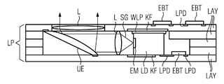
1 shows an optical signal transmitter comprising a semiconductor based light source and a refractive element in the structural space between outer layers of a multilayer printed circuit board.
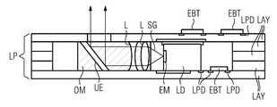
FIG. 2 shows an arrangement corresponding to FIG. 1, in which an optical module is provided comprising a refractive element and a plurality of lenses in the structural space.
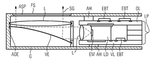
3 shows an optical signal transmitter comprising a semiconductor based light source in the structural space between outer layers of a multilayer printed circuit board, wherein the refractive elements are arranged outside the printed circuit board arrangement.
1 illustrates an optical signal transmitter in cross section. In this case, a printed circuit board LP consisting of five layers LAY is illustrated, where the structural space for the active elements of the optical signal transmitter is provided in the area where only the outer layers LAY are present. A semiconductor based light source, here a laser diode (LD), is provided as the active element. The laser diode LD is electrically connected to the solder pad LPD of the lower outer layer LAY of the printed circuit board, the housing surfaces of which lie on the cooling surfaces KF of the printed circuit board LP. . 1, in the upper region of the laser diode LD, a heat conduction pad WLP is arranged between the laser diode LD and the cooling surface KF, the heat conduction pad being parallel to the heat transfer. The gap between the LD and the upper layer LAY of the printed circuit board LP is filled.
1 shows additional electronic components (EBT) that are not necessarily associated with the functionality of an optical signal transmitter. The emitter EM of the laser diode LD has its surface oriented perpendicular to the base surface of the printed circuit board LP, ie the generated light is parallel to the layers of the printed circuit board (in FIG. 1). Toward the left). In order to focus the light-the beam path SG is schematically shown in FIG. 1-lenses L are provided, which are accompanied by a schematic illustration, and in addition to the two lenses L shown Complex lens systems can also be used. Finally, in the structural space, the mirror is provided at an oblique position as the refractive element UE, which refracts the emitted light in a direction perpendicular to the faces of the printed circuit board LP (here: upwards). Light exits through an opening in the top layer of the printed circuit board LP, which in this example embodiment is a transparent closing element FS ("filter disk") that serves as an additional lens L used for beam shaping. Have In the present exemplary embodiment, the surface of the refractive element UE (here: mirror) is not embodied in a planar fashion, but rather curved. As a result, shaping (focusing) of the emitted light beam is additionally achieved.
The laser diode LD is directly wired to a solder pad LPD in which an "unpackaged" semiconductor component, i.e., an unpackaged "die", is used as a printed circuit board LP or a contact area. For this purpose, the technique of "chip bonding" is used here, and likewise other contact-making techniques can be used. Instead of a multilayer printed circuit board LP, in which the individual layers LAY are bonded and bonded (laminated) to each other under pressure, an arrangement according to the invention may be constructed from individually loaded printed circuit boards ("printed circuit Board loading ").
2 shows an optical signal transmitter in which optical elements are coupled into an optical module OM. The remaining component parts substantially correspond to the arrangement from FIG. 1, and therefore its component parts and reference symbols will not be described again at this point. However, in connection with FIG. 2, in the upper layer LAY of the printed circuit board LP, in this case the lens is not used as an element for beam shaping (focusing), but rather only an opening ASP (“cut out”). It is used as). As a result, during mounting, the optical module OM needs to be precisely aligned with the opening ASP or the transparent covering (closed element FS) of the top layer LAY of the printed circuit board LP in an alternative exemplary embodiment. none.
3 shows that only the semiconductor-based light source and, if appropriate, the lens L or the lens system (objective) are integrated into the printed circuit board LP, the refractive element UE, and, if appropriate, no further optical elements, are incorporated. Illustrates an embodiment of an optical signal transmitter. As a result, larger dimensions can be given to the optical elements, in particular the refractive element UE. This solution is particularly advantageous in cases where the printed circuit board LP is again installed in a separate housing G having a receptacle AOE for the optical elements. The spacers AH between the housing G and the upper layer OL and the lower layer UL of the printed circuit board LP each serve to firstly fix the printed circuit board LP and secondly to the refractive element. (UE) and other external optical elements and the printed circuit board LP, and thus the light emitter EM.
The optical receiver (photo detector) for the optical sensor may also be configured similarly to the optical signal transmitter illustrated with reference to FIGS. In this case, a semiconductor based light detector such as a CCD sensor or a CMOS sensor is used instead of the semiconductor based light source. In this case, the beam path SG of light is the same, and the beam direction is of course reversed.
Claims (11)
Semiconductor based light source (LD) for generating light
/ RTI >
The semiconductor based light source LD is arranged in the structural space between the outer layers OL and UL of the multilayer printed circuit board LP,
The light exit direction of the semiconductor based light source LD is oriented substantially parallel to the layers LAY of the printed circuit board LP,
A refraction unit UE is provided for refracting light emitted by the semiconductor based light source LD in a direction substantially perpendicular to the layers LAY of the printed circuit board LP. Signal transmitter.
The refractive element (UE) is arranged in the structural space.
For the emission of refracted light, one of the outer layers OL, UL of the printed circuit board LP has an opening ASP or a transparent closing element FS in the region of the refractive element UE. An optical signal transmitter.
The refractive element UE is arranged at the end side along the printed circuit board LP in the direction of light output of the semiconductor based light source LP, and the structural space is an end side exit opening or end side for the light. Optical signal transmitter, characterized in that it has a transparent closing element (FS).
And the refractive element (UE) is a prism or a mirror.
The reflective surface of the refractive element (UE) is embodied convex or concave for concentrating or expanding the light beam.
And said refractive element (UE) and at least one optical lens (L) combine to form an optical module (OM).
The semiconductor based light source (LD) is in contact with the contact area (KF) of the printed circuit board (LP) for the purpose of heat dissipation.
The semiconductor-based light source LD is electrically connected to conductor tracks or contact regions LPD of the printed circuit board LP by bonding or plated-through holes. Optical signal transmitter.
Semiconductor based photo detector for detecting light
Including;
The semiconductor based photodetector is arranged in the structural space between the outer layers OL, UL of the multilayer printed circuit board LP,
The photosensitive detector region of the semiconductor based photo detector is oriented substantially perpendicular to the layers LAY of the printed circuit board LP,
And a refraction unit (UE) is provided for refracting light to be detected by said semiconductor based photo detector from a direction substantially perpendicular to said layers (LAY) of said printed circuit board (LP).
And the semiconductor based photo detector is a CCD sensor or a CMOS sensor.
Applications Claiming Priority (2)
| Application Number | Priority Date | Filing Date | Title |
|---|---|---|---|
| DE200910051188 DE102009051188A1 (en) | 2009-10-29 | 2009-10-29 | Light signal transmitter and light receiver for an optical sensor |
| DE102009051188.1 | 2009-10-29 |
Publications (1)
| Publication Number | Publication Date |
|---|---|
| KR20120101357A true KR20120101357A (en) | 2012-09-13 |
Family
ID=43797830
Family Applications (1)
| Application Number | Title | Priority Date | Filing Date |
|---|---|---|---|
| KR1020127010615A KR20120101357A (en) | 2009-10-29 | 2010-10-28 | Light signal transmitter and light receiver for an optical sensor |
Country Status (6)
| Country | Link |
|---|---|
| US (1) | US8851733B2 (en) |
| EP (1) | EP2494384A2 (en) |
| JP (1) | JP2013509699A (en) |
| KR (1) | KR20120101357A (en) |
| DE (1) | DE102009051188A1 (en) |
| WO (1) | WO2011051370A2 (en) |
Families Citing this family (8)
| Publication number | Priority date | Publication date | Assignee | Title |
|---|---|---|---|---|
| DE102009051188A1 (en) | 2009-10-29 | 2011-05-19 | Siemens Aktiengesellschaft | Light signal transmitter and light receiver for an optical sensor |
| TWI511005B (en) * | 2013-12-20 | 2015-12-01 | Qisda Corp | Display device and infrared touch module thereof |
| DE102016107153B4 (en) * | 2016-04-18 | 2018-10-18 | Sick Ag | Optoelectronic sensor |
| CN106547033B (en) * | 2016-09-28 | 2018-08-07 | 西北工业大学 | A kind of moveable micro-nano polarization grating array apparatus and its application method |
| DE102016121913A1 (en) | 2016-11-15 | 2018-05-17 | Sick Ag | Multibeam light barrier |
| DE202016106394U1 (en) | 2016-11-15 | 2018-02-16 | Sick Ag | Multibeam light barrier |
| DE102019118978A1 (en) * | 2019-07-12 | 2021-01-14 | OSRAM CONTINENTAL GmbH | Optical arrangement and vehicle |
| CN112216656B (en) * | 2020-09-02 | 2021-07-06 | 珠海越亚半导体股份有限公司 | Cavity substrate with directional photoelectric transmission channel and manufacturing method thereof |
Family Cites Families (24)
| Publication number | Priority date | Publication date | Assignee | Title |
|---|---|---|---|---|
| DE4407967C2 (en) | 1994-03-10 | 1997-11-20 | Leuze Electronic Gmbh & Co | Electronic device |
| EP0718974B1 (en) * | 1994-12-22 | 2002-08-28 | Optosys Ag | Proximity switch |
| JPH09318853A (en) * | 1996-03-29 | 1997-12-12 | Sony Corp | Optical transmission/reception equipment and optical communication network |
| JPH10256648A (en) | 1997-03-13 | 1998-09-25 | Hitachi Ltd | Laser diode module |
| DE19858247C1 (en) * | 1998-12-17 | 2000-01-27 | Leuze Electronic Gmbh & Co | Opto-electronic arrangement for detecting objects in a monitoring region enables highly effective screening of the transmitter and/or receiver |
| DE19947889C2 (en) * | 1999-10-05 | 2003-03-06 | Infineon Technologies Ag | Optoelectronic, bidirectional transmit and receive module in leadframe technology |
| AT5153U1 (en) * | 2001-03-22 | 2002-03-25 | Avl List Gmbh | OPTICAL SENSOR FOR DETECTING COMBUSTION |
| DE10308085B4 (en) * | 2002-03-08 | 2006-09-07 | Leuze Electronic Gmbh & Co Kg | Optoelectronic device |
| JP2004061799A (en) * | 2002-07-29 | 2004-02-26 | Canon Inc | Two-dimensional waveguide apparatus and opto-electronic fusion wiring board using same |
| KR100449876B1 (en) * | 2002-12-05 | 2004-09-22 | 삼성전기주식회사 | A multi-layer PCB for connecting multi-channel optical signals of block type, and methods thereof |
| KR100451635B1 (en) * | 2002-12-10 | 2004-10-08 | 삼성전기주식회사 | Fiber blocks and pipe blocks, and methods for connecting optical signals of multi-layer PCB by using them |
| KR100499005B1 (en) * | 2002-12-27 | 2005-07-01 | 삼성전기주식회사 | A printed circuit board being packaged optical devices of multi-channel block type |
| KR100528972B1 (en) * | 2003-10-27 | 2005-11-16 | 한국전자통신연구원 | Optical printed circuit board system with taper shaped-waveguides |
| DE102004028814A1 (en) * | 2004-06-15 | 2006-01-05 | Siemens Ag | Printed circuit board, has light conductor unit arranged between printed circuit board layers, where one layer has passage opening lined with material whose refractive index is similar to that of light conductor unit |
| US7228020B2 (en) * | 2004-08-31 | 2007-06-05 | Finisar Corporation | Optoelectronic arrangement having a surface-mountable semiconductor module and a cooling element |
| US7350934B2 (en) * | 2005-05-03 | 2008-04-01 | Delphi Technologies, Inc. | Illuminated display system |
| AT503585B1 (en) * | 2006-05-08 | 2007-11-15 | Austria Tech & System Tech | PCB ELEMENT ELEMENT AND METHOD FOR THE PRODUCTION THEREOF |
| AT503027B1 (en) * | 2006-05-08 | 2007-07-15 | Austria Tech & System Tech | Printed circuit board element for multi-mode or single mode waveguide data transmission, has opto-electronic component embedded in optical photo-polymerizable layered material, and component has curved deviation mirror |
| JP2008084396A (en) * | 2006-09-27 | 2008-04-10 | Matsushita Electric Ind Co Ltd | Semiconductor device, method of manufacturing semiconductor device, optical pickup device and optical disk drive device |
| EP2082167B1 (en) * | 2006-10-16 | 2017-02-22 | Philips Lighting Holding B.V. | Light emitting diode lighting device |
| CN101529156B (en) * | 2006-10-16 | 2012-03-21 | 皇家飞利浦电子股份有限公司 | Lighting device |
| AT505834B1 (en) * | 2007-09-21 | 2009-09-15 | Austria Tech & System Tech | CIRCUIT BOARD ELEMENT |
| US7541058B2 (en) * | 2007-10-09 | 2009-06-02 | Endicott Interconnect Technologies, Inc. | Method of making circuitized substrate with internal optical pathway |
| DE102009051188A1 (en) | 2009-10-29 | 2011-05-19 | Siemens Aktiengesellschaft | Light signal transmitter and light receiver for an optical sensor |
-
2009
- 2009-10-29 DE DE200910051188 patent/DE102009051188A1/en not_active Ceased
-
2010
- 2010-10-28 KR KR1020127010615A patent/KR20120101357A/en not_active Application Discontinuation
- 2010-10-28 WO PCT/EP2010/066318 patent/WO2011051370A2/en active Application Filing
- 2010-10-28 US US13/504,987 patent/US8851733B2/en not_active Expired - Fee Related
- 2010-10-28 EP EP10775774A patent/EP2494384A2/en not_active Withdrawn
- 2010-10-28 JP JP2012535820A patent/JP2013509699A/en active Pending
Also Published As
| Publication number | Publication date |
|---|---|
| EP2494384A2 (en) | 2012-09-05 |
| DE102009051188A1 (en) | 2011-05-19 |
| JP2013509699A (en) | 2013-03-14 |
| US20120218766A1 (en) | 2012-08-30 |
| US8851733B2 (en) | 2014-10-07 |
| WO2011051370A2 (en) | 2011-05-05 |
| WO2011051370A3 (en) | 2012-04-19 |
Similar Documents
| Publication | Publication Date | Title |
|---|---|---|
| KR20120101357A (en) | Light signal transmitter and light receiver for an optical sensor | |
| US9134224B2 (en) | Gas component detection device | |
| JP2013509699A5 (en) | ||
| JP2017523467A (en) | Luminescent body and photodetection module including vertical alignment mechanism | |
| US20060110110A1 (en) | Optical turn system for optoelectronic modules | |
| US6097521A (en) | Optoelectronic module for bidirectional optical data transmission | |
| JP2005234052A (en) | Optical transmission and reception module | |
| JPWO2014136414A1 (en) | device | |
| KR101386794B1 (en) | Light detecting device | |
| JP6476634B2 (en) | Optical receiver module | |
| JP4604036B2 (en) | Optical module and optical system | |
| USRE38280E1 (en) | Optoelectronic module for bidirectional optical data transmission | |
| KR20210035193A (en) | Spectrometer device and method of manufacturing the spectrometer device | |
| US20050276546A1 (en) | Bidirectional emitting and receiving module | |
| JP5266859B2 (en) | Photoelectric sensor | |
| JP7123599B2 (en) | Light receiving and emitting device and optical density measuring device | |
| JP2013120155A (en) | Gas component detector | |
| JP2004279892A (en) | Bidirectional optical module | |
| KR101317586B1 (en) | Light detecting device | |
| KR20170090593A (en) | light module | |
| TW201518690A (en) | Optical encoder modules that include a telecentric imaging system | |
| TW201518691A (en) | Optical encoder modules | |
| JP2009020201A (en) | Optical module | |
| JPS5982779A (en) | Mounting method of optical integrated circuit | |
| JP2011204766A (en) | Light-emitting device |
Legal Events
| Date | Code | Title | Description |
|---|---|---|---|
| A201 | Request for examination | ||
| E902 | Notification of reason for refusal | ||
| E601 | Decision to refuse application |