KR20120071802A - Methods of forming semiconductor devices - Google Patents
Methods of forming semiconductor devices Download PDFInfo
- Publication number
- KR20120071802A KR20120071802A KR1020100133492A KR20100133492A KR20120071802A KR 20120071802 A KR20120071802 A KR 20120071802A KR 1020100133492 A KR1020100133492 A KR 1020100133492A KR 20100133492 A KR20100133492 A KR 20100133492A KR 20120071802 A KR20120071802 A KR 20120071802A
- Authority
- KR
- South Korea
- Prior art keywords
- etching
- plasma
- substrate
- region
- forming
- Prior art date
Links
- 238000000034 method Methods 0.000 title claims abstract description 218
- 239000004065 semiconductor Substances 0.000 title claims abstract description 73
- 238000005530 etching Methods 0.000 claims abstract description 167
- 239000000758 substrate Substances 0.000 claims abstract description 66
- 239000001257 hydrogen Substances 0.000 claims abstract description 39
- 229910052739 hydrogen Inorganic materials 0.000 claims abstract description 39
- UFHFLCQGNIYNRP-UHFFFAOYSA-N Hydrogen Chemical compound [H][H] UFHFLCQGNIYNRP-UHFFFAOYSA-N 0.000 claims abstract description 11
- 239000007789 gas Substances 0.000 claims description 79
- 125000004435 hydrogen atom Chemical group [H]* 0.000 claims description 22
- 238000006467 substitution reaction Methods 0.000 claims description 22
- QGZKDVFQNNGYKY-UHFFFAOYSA-N Ammonia Chemical compound N QGZKDVFQNNGYKY-UHFFFAOYSA-N 0.000 claims description 16
- 238000000866 electrolytic etching Methods 0.000 claims description 15
- 150000001875 compounds Chemical class 0.000 claims description 11
- KRHYYFGTRYWZRS-UHFFFAOYSA-N Fluorane Chemical compound F KRHYYFGTRYWZRS-UHFFFAOYSA-N 0.000 claims description 10
- 229910021529 ammonia Inorganic materials 0.000 claims description 8
- 238000010438 heat treatment Methods 0.000 claims description 8
- 229910000040 hydrogen fluoride Inorganic materials 0.000 claims description 6
- IGELFKKMDLGCJO-UHFFFAOYSA-N xenon difluoride Chemical compound F[Xe]F IGELFKKMDLGCJO-UHFFFAOYSA-N 0.000 claims description 6
- PXGOKWXKJXAPGV-UHFFFAOYSA-N Fluorine Chemical compound FF PXGOKWXKJXAPGV-UHFFFAOYSA-N 0.000 claims description 5
- 229910052731 fluorine Inorganic materials 0.000 claims description 5
- 239000011737 fluorine Substances 0.000 claims description 5
- GVGCUCJTUSOZKP-UHFFFAOYSA-N nitrogen trifluoride Chemical compound FN(F)F GVGCUCJTUSOZKP-UHFFFAOYSA-N 0.000 claims description 4
- 239000004020 conductor Substances 0.000 abstract description 15
- 239000010410 layer Substances 0.000 description 75
- 239000011229 interlayer Substances 0.000 description 34
- 229910052751 metal Inorganic materials 0.000 description 15
- 239000002184 metal Substances 0.000 description 15
- 150000004767 nitrides Chemical class 0.000 description 15
- 229910052721 tungsten Inorganic materials 0.000 description 12
- 239000010937 tungsten Substances 0.000 description 12
- 230000015572 biosynthetic process Effects 0.000 description 10
- 229910052736 halogen Inorganic materials 0.000 description 10
- XUIMIQQOPSSXEZ-UHFFFAOYSA-N Silicon Chemical compound [Si] XUIMIQQOPSSXEZ-UHFFFAOYSA-N 0.000 description 9
- 229910052710 silicon Inorganic materials 0.000 description 9
- 239000010703 silicon Substances 0.000 description 9
- XKRFYHLGVUSROY-UHFFFAOYSA-N Argon Chemical compound [Ar] XKRFYHLGVUSROY-UHFFFAOYSA-N 0.000 description 8
- IJGRMHOSHXDMSA-UHFFFAOYSA-N Atomic nitrogen Chemical compound N#N IJGRMHOSHXDMSA-UHFFFAOYSA-N 0.000 description 8
- -1 fluorine-bromine compound Chemical class 0.000 description 8
- NRTOMJZYCJJWKI-UHFFFAOYSA-N Titanium nitride Chemical compound [Ti]#N NRTOMJZYCJJWKI-UHFFFAOYSA-N 0.000 description 7
- 239000000463 material Substances 0.000 description 7
- RTAQQCXQSZGOHL-UHFFFAOYSA-N Titanium Chemical compound [Ti] RTAQQCXQSZGOHL-UHFFFAOYSA-N 0.000 description 6
- 239000003990 capacitor Substances 0.000 description 6
- 238000005229 chemical vapour deposition Methods 0.000 description 6
- 239000011261 inert gas Substances 0.000 description 6
- 229910052715 tantalum Inorganic materials 0.000 description 6
- GUVRBAGPIYLISA-UHFFFAOYSA-N tantalum atom Chemical compound [Ta] GUVRBAGPIYLISA-UHFFFAOYSA-N 0.000 description 6
- MZLGASXMSKOWSE-UHFFFAOYSA-N tantalum nitride Chemical compound [Ta]#N MZLGASXMSKOWSE-UHFFFAOYSA-N 0.000 description 6
- 239000010936 titanium Substances 0.000 description 6
- 229910052719 titanium Inorganic materials 0.000 description 6
- WFKWXMTUELFFGS-UHFFFAOYSA-N tungsten Chemical compound [W] WFKWXMTUELFFGS-UHFFFAOYSA-N 0.000 description 6
- VYPSYNLAJGMNEJ-UHFFFAOYSA-N Silicium dioxide Chemical compound O=[Si]=O VYPSYNLAJGMNEJ-UHFFFAOYSA-N 0.000 description 5
- 125000004429 atom Chemical group 0.000 description 5
- 238000004519 manufacturing process Methods 0.000 description 5
- 238000005240 physical vapour deposition Methods 0.000 description 5
- 229910052814 silicon oxide Inorganic materials 0.000 description 5
- 229910052786 argon Inorganic materials 0.000 description 4
- 238000000231 atomic layer deposition Methods 0.000 description 4
- 238000010586 diagram Methods 0.000 description 4
- 239000003989 dielectric material Substances 0.000 description 4
- 238000002955 isolation Methods 0.000 description 4
- 229910052757 nitrogen Inorganic materials 0.000 description 4
- 229910021420 polycrystalline silicon Inorganic materials 0.000 description 4
- 238000003860 storage Methods 0.000 description 4
- WQJQOUPTWCFRMM-UHFFFAOYSA-N tungsten disilicide Chemical compound [Si]#[W]#[Si] WQJQOUPTWCFRMM-UHFFFAOYSA-N 0.000 description 4
- 229910021342 tungsten silicide Inorganic materials 0.000 description 4
- 229910052581 Si3N4 Inorganic materials 0.000 description 3
- 239000011810 insulating material Substances 0.000 description 3
- HQVNEWCFYHHQES-UHFFFAOYSA-N silicon nitride Chemical compound N12[Si]34N5[Si]62N3[Si]51N64 HQVNEWCFYHHQES-UHFFFAOYSA-N 0.000 description 3
- KJTLSVCANCCWHF-UHFFFAOYSA-N Ruthenium Chemical compound [Ru] KJTLSVCANCCWHF-UHFFFAOYSA-N 0.000 description 2
- HXELGNKCCDGMMN-UHFFFAOYSA-N [F].[Cl] Chemical compound [F].[Cl] HXELGNKCCDGMMN-UHFFFAOYSA-N 0.000 description 2
- RNIPBGMVTAUWNH-UHFFFAOYSA-N [F].[I] Chemical compound [F].[I] RNIPBGMVTAUWNH-UHFFFAOYSA-N 0.000 description 2
- 230000009977 dual effect Effects 0.000 description 2
- 230000006870 function Effects 0.000 description 2
- 150000002367 halogens Chemical class 0.000 description 2
- 229910052741 iridium Inorganic materials 0.000 description 2
- GKOZUEZYRPOHIO-UHFFFAOYSA-N iridium atom Chemical compound [Ir] GKOZUEZYRPOHIO-UHFFFAOYSA-N 0.000 description 2
- 229910044991 metal oxide Inorganic materials 0.000 description 2
- 150000004706 metal oxides Chemical class 0.000 description 2
- 229910052707 ruthenium Inorganic materials 0.000 description 2
- 101100028951 Homo sapiens PDIA2 gene Proteins 0.000 description 1
- 102100036351 Protein disulfide-isomerase A2 Human genes 0.000 description 1
- 229910000577 Silicon-germanium Inorganic materials 0.000 description 1
- LEVVHYCKPQWKOP-UHFFFAOYSA-N [Si].[Ge] Chemical compound [Si].[Ge] LEVVHYCKPQWKOP-UHFFFAOYSA-N 0.000 description 1
- 238000007792 addition Methods 0.000 description 1
- 238000003491 array Methods 0.000 description 1
- 239000000969 carrier Substances 0.000 description 1
- 239000000919 ceramic Substances 0.000 description 1
- 238000004891 communication Methods 0.000 description 1
- 230000000295 complement effect Effects 0.000 description 1
- 238000013500 data storage Methods 0.000 description 1
- HTXDPTMKBJXEOW-UHFFFAOYSA-N dioxoiridium Chemical compound O=[Ir]=O HTXDPTMKBJXEOW-UHFFFAOYSA-N 0.000 description 1
- 229910052732 germanium Inorganic materials 0.000 description 1
- GNPVGFCGXDBREM-UHFFFAOYSA-N germanium atom Chemical compound [Ge] GNPVGFCGXDBREM-UHFFFAOYSA-N 0.000 description 1
- 229910000449 hafnium oxide Inorganic materials 0.000 description 1
- WIHZLLGSGQNAGK-UHFFFAOYSA-N hafnium(4+);oxygen(2-) Chemical compound [O-2].[O-2].[Hf+4] WIHZLLGSGQNAGK-UHFFFAOYSA-N 0.000 description 1
- 239000012535 impurity Substances 0.000 description 1
- 230000010354 integration Effects 0.000 description 1
- 229910000457 iridium oxide Inorganic materials 0.000 description 1
- 150000002739 metals Chemical class 0.000 description 1
- TWNQGVIAIRXVLR-UHFFFAOYSA-N oxo(oxoalumanyloxy)alumane Chemical compound O=[Al]O[Al]=O TWNQGVIAIRXVLR-UHFFFAOYSA-N 0.000 description 1
- 238000000059 patterning Methods 0.000 description 1
- 230000004044 response Effects 0.000 description 1
- 229910021332 silicide Inorganic materials 0.000 description 1
- 239000002356 single layer Substances 0.000 description 1
- 239000007787 solid Substances 0.000 description 1
- 239000000126 substance Substances 0.000 description 1
Images


Classifications
-
- H—ELECTRICITY
- H01—ELECTRIC ELEMENTS
- H01L—SEMICONDUCTOR DEVICES NOT COVERED BY CLASS H10
- H01L21/00—Processes or apparatus adapted for the manufacture or treatment of semiconductor or solid state devices or of parts thereof
- H01L21/02—Manufacture or treatment of semiconductor devices or of parts thereof
- H01L21/02041—Cleaning
- H01L21/02057—Cleaning during device manufacture
- H01L21/0206—Cleaning during device manufacture during, before or after processing of insulating layers
- H01L21/02063—Cleaning during device manufacture during, before or after processing of insulating layers the processing being the formation of vias or contact holes
-
- H—ELECTRICITY
- H01—ELECTRIC ELEMENTS
- H01L—SEMICONDUCTOR DEVICES NOT COVERED BY CLASS H10
- H01L21/00—Processes or apparatus adapted for the manufacture or treatment of semiconductor or solid state devices or of parts thereof
- H01L21/02—Manufacture or treatment of semiconductor devices or of parts thereof
- H01L21/02104—Forming layers
- H01L21/02107—Forming insulating materials on a substrate
- H01L21/02296—Forming insulating materials on a substrate characterised by the treatment performed before or after the formation of the layer
- H01L21/02299—Forming insulating materials on a substrate characterised by the treatment performed before or after the formation of the layer pre-treatment
- H01L21/02312—Forming insulating materials on a substrate characterised by the treatment performed before or after the formation of the layer pre-treatment treatment by exposure to a gas or vapour
- H01L21/02315—Forming insulating materials on a substrate characterised by the treatment performed before or after the formation of the layer pre-treatment treatment by exposure to a gas or vapour treatment by exposure to a plasma
-
- H—ELECTRICITY
- H01—ELECTRIC ELEMENTS
- H01L—SEMICONDUCTOR DEVICES NOT COVERED BY CLASS H10
- H01L21/00—Processes or apparatus adapted for the manufacture or treatment of semiconductor or solid state devices or of parts thereof
- H01L21/02—Manufacture or treatment of semiconductor devices or of parts thereof
- H01L21/04—Manufacture or treatment of semiconductor devices or of parts thereof the devices having at least one potential-jump barrier or surface barrier, e.g. PN junction, depletion layer or carrier concentration layer
- H01L21/18—Manufacture or treatment of semiconductor devices or of parts thereof the devices having at least one potential-jump barrier or surface barrier, e.g. PN junction, depletion layer or carrier concentration layer the devices having semiconductor bodies comprising elements of Group IV of the Periodic System or AIIIBV compounds with or without impurities, e.g. doping materials
- H01L21/30—Treatment of semiconductor bodies using processes or apparatus not provided for in groups H01L21/20 - H01L21/26
- H01L21/302—Treatment of semiconductor bodies using processes or apparatus not provided for in groups H01L21/20 - H01L21/26 to change their surface-physical characteristics or shape, e.g. etching, polishing, cutting
- H01L21/306—Chemical or electrical treatment, e.g. electrolytic etching
- H01L21/3065—Plasma etching; Reactive-ion etching
-
- H—ELECTRICITY
- H01—ELECTRIC ELEMENTS
- H01L—SEMICONDUCTOR DEVICES NOT COVERED BY CLASS H10
- H01L21/00—Processes or apparatus adapted for the manufacture or treatment of semiconductor or solid state devices or of parts thereof
- H01L21/02—Manufacture or treatment of semiconductor devices or of parts thereof
- H01L21/04—Manufacture or treatment of semiconductor devices or of parts thereof the devices having at least one potential-jump barrier or surface barrier, e.g. PN junction, depletion layer or carrier concentration layer
- H01L21/18—Manufacture or treatment of semiconductor devices or of parts thereof the devices having at least one potential-jump barrier or surface barrier, e.g. PN junction, depletion layer or carrier concentration layer the devices having semiconductor bodies comprising elements of Group IV of the Periodic System or AIIIBV compounds with or without impurities, e.g. doping materials
- H01L21/30—Treatment of semiconductor bodies using processes or apparatus not provided for in groups H01L21/20 - H01L21/26
- H01L21/31—Treatment of semiconductor bodies using processes or apparatus not provided for in groups H01L21/20 - H01L21/26 to form insulating layers thereon, e.g. for masking or by using photolithographic techniques; After treatment of these layers; Selection of materials for these layers
- H01L21/3105—After-treatment
- H01L21/311—Etching the insulating layers by chemical or physical means
- H01L21/31105—Etching inorganic layers
- H01L21/31111—Etching inorganic layers by chemical means
- H01L21/31116—Etching inorganic layers by chemical means by dry-etching
-
- H—ELECTRICITY
- H01—ELECTRIC ELEMENTS
- H01L—SEMICONDUCTOR DEVICES NOT COVERED BY CLASS H10
- H01L21/00—Processes or apparatus adapted for the manufacture or treatment of semiconductor or solid state devices or of parts thereof
- H01L21/02—Manufacture or treatment of semiconductor devices or of parts thereof
- H01L21/04—Manufacture or treatment of semiconductor devices or of parts thereof the devices having at least one potential-jump barrier or surface barrier, e.g. PN junction, depletion layer or carrier concentration layer
- H01L21/18—Manufacture or treatment of semiconductor devices or of parts thereof the devices having at least one potential-jump barrier or surface barrier, e.g. PN junction, depletion layer or carrier concentration layer the devices having semiconductor bodies comprising elements of Group IV of the Periodic System or AIIIBV compounds with or without impurities, e.g. doping materials
- H01L21/30—Treatment of semiconductor bodies using processes or apparatus not provided for in groups H01L21/20 - H01L21/26
- H01L21/324—Thermal treatment for modifying the properties of semiconductor bodies, e.g. annealing, sintering
-
- H—ELECTRICITY
- H01—ELECTRIC ELEMENTS
- H01L—SEMICONDUCTOR DEVICES NOT COVERED BY CLASS H10
- H01L21/00—Processes or apparatus adapted for the manufacture or treatment of semiconductor or solid state devices or of parts thereof
- H01L21/70—Manufacture or treatment of devices consisting of a plurality of solid state components formed in or on a common substrate or of parts thereof; Manufacture of integrated circuit devices or of parts thereof
- H01L21/71—Manufacture of specific parts of devices defined in group H01L21/70
- H01L21/768—Applying interconnections to be used for carrying current between separate components within a device comprising conductors and dielectrics
- H01L21/76801—Applying interconnections to be used for carrying current between separate components within a device comprising conductors and dielectrics characterised by the formation and the after-treatment of the dielectrics, e.g. smoothing
- H01L21/76802—Applying interconnections to be used for carrying current between separate components within a device comprising conductors and dielectrics characterised by the formation and the after-treatment of the dielectrics, e.g. smoothing by forming openings in dielectrics
- H01L21/76805—Applying interconnections to be used for carrying current between separate components within a device comprising conductors and dielectrics characterised by the formation and the after-treatment of the dielectrics, e.g. smoothing by forming openings in dielectrics the opening being a via or contact hole penetrating the underlying conductor
-
- H—ELECTRICITY
- H01—ELECTRIC ELEMENTS
- H01L—SEMICONDUCTOR DEVICES NOT COVERED BY CLASS H10
- H01L21/00—Processes or apparatus adapted for the manufacture or treatment of semiconductor or solid state devices or of parts thereof
- H01L21/70—Manufacture or treatment of devices consisting of a plurality of solid state components formed in or on a common substrate or of parts thereof; Manufacture of integrated circuit devices or of parts thereof
- H01L21/71—Manufacture of specific parts of devices defined in group H01L21/70
- H01L21/768—Applying interconnections to be used for carrying current between separate components within a device comprising conductors and dielectrics
- H01L21/76801—Applying interconnections to be used for carrying current between separate components within a device comprising conductors and dielectrics characterised by the formation and the after-treatment of the dielectrics, e.g. smoothing
- H01L21/76802—Applying interconnections to be used for carrying current between separate components within a device comprising conductors and dielectrics characterised by the formation and the after-treatment of the dielectrics, e.g. smoothing by forming openings in dielectrics
- H01L21/76814—Applying interconnections to be used for carrying current between separate components within a device comprising conductors and dielectrics characterised by the formation and the after-treatment of the dielectrics, e.g. smoothing by forming openings in dielectrics post-treatment or after-treatment, e.g. cleaning or removal of oxides on underlying conductors
-
- H—ELECTRICITY
- H01—ELECTRIC ELEMENTS
- H01L—SEMICONDUCTOR DEVICES NOT COVERED BY CLASS H10
- H01L21/00—Processes or apparatus adapted for the manufacture or treatment of semiconductor or solid state devices or of parts thereof
- H01L21/70—Manufacture or treatment of devices consisting of a plurality of solid state components formed in or on a common substrate or of parts thereof; Manufacture of integrated circuit devices or of parts thereof
- H01L21/71—Manufacture of specific parts of devices defined in group H01L21/70
- H01L21/768—Applying interconnections to be used for carrying current between separate components within a device comprising conductors and dielectrics
- H01L21/76801—Applying interconnections to be used for carrying current between separate components within a device comprising conductors and dielectrics characterised by the formation and the after-treatment of the dielectrics, e.g. smoothing
- H01L21/76822—Modification of the material of dielectric layers, e.g. grading, after-treatment to improve the stability of the layers, to increase their density etc.
- H01L21/76826—Modification of the material of dielectric layers, e.g. grading, after-treatment to improve the stability of the layers, to increase their density etc. by contacting the layer with gases, liquids or plasmas
-
- H—ELECTRICITY
- H05—ELECTRIC TECHNIQUES NOT OTHERWISE PROVIDED FOR
- H05H—PLASMA TECHNIQUE; PRODUCTION OF ACCELERATED ELECTRICALLY-CHARGED PARTICLES OR OF NEUTRONS; PRODUCTION OR ACCELERATION OF NEUTRAL MOLECULAR OR ATOMIC BEAMS
- H05H1/00—Generating plasma; Handling plasma
- H05H1/24—Generating plasma
- H05H1/46—Generating plasma using applied electromagnetic fields, e.g. high frequency or microwave energy
-
- H—ELECTRICITY
- H10—SEMICONDUCTOR DEVICES; ELECTRIC SOLID-STATE DEVICES NOT OTHERWISE PROVIDED FOR
- H10B—ELECTRONIC MEMORY DEVICES
- H10B12/00—Dynamic random access memory [DRAM] devices
- H10B12/01—Manufacture or treatment
- H10B12/02—Manufacture or treatment for one transistor one-capacitor [1T-1C] memory cells
- H10B12/03—Making the capacitor or connections thereto
- H10B12/033—Making the capacitor or connections thereto the capacitor extending over the transistor
- H10B12/0335—Making a connection between the transistor and the capacitor, e.g. plug
-
- H—ELECTRICITY
- H10—SEMICONDUCTOR DEVICES; ELECTRIC SOLID-STATE DEVICES NOT OTHERWISE PROVIDED FOR
- H10B—ELECTRONIC MEMORY DEVICES
- H10B12/00—Dynamic random access memory [DRAM] devices
- H10B12/30—DRAM devices comprising one-transistor - one-capacitor [1T-1C] memory cells
- H10B12/48—Data lines or contacts therefor
- H10B12/485—Bit line contacts
Abstract
Description
본 발명은 반도체 장치의 형성 방법에 관한 것이다.The present invention relates to a method of forming a semiconductor device.
최근 휴대폰, 노트북 등의 전자산업에서 제품의 경량화, 소형화, 고속화, 다기능화, 고성능화, 높은 신뢰성 및 저렴한 가격에 대한 요구가 증가하고 있다. 이러한 요구를 충족시키기 위해서, 반도체 장치의 집적도를 증가시키고 반도체 장치의 공정 마진을 확보하는 것뿐만 아니라 상기 반도체 장치의 전기적 특성 및 신뢰성을 개선하는 것이 요구되고 있다.Recently, in the electronic industry, such as mobile phones and laptops, there is an increasing demand for light weight, miniaturization, high speed, multifunction, high performance, high reliability, and low price. In order to meet such demands, there is a demand for increasing the degree of integration of semiconductor devices and securing process margins of semiconductor devices, as well as improving electrical characteristics and reliability of the semiconductor devices.
특히, 반도체 장치에서 상기 요구들을 충족시키기 위해서, 반도체 장치의 제조 공정에 대한 다양한 연구들이 이루어지고 있다.In particular, in order to meet the above demands in semiconductor devices, various studies on the manufacturing process of semiconductor devices have been made.
본 발명의 실시 예들이 해결하고자 하는 일 기술적 과제는 신뢰성 및 전기적 특성이 향상된 반도체 장치의 형성 방법을 제공하는데 있다.One technical problem to be solved by the embodiments of the present invention is to provide a method of forming a semiconductor device with improved reliability and electrical characteristics.
본 발명의 실시 예들이 해결하고자 하는 다른 기술적 과제는 공정 마진을 확보할 수 있는 반도체 장치의 형성 방법을 제공하는데 있다.Another technical problem to be solved by the embodiments of the present invention is to provide a method of forming a semiconductor device that can secure a process margin.
상술한 기술적 과제들을 해결하기 위한 반도체 장치의 형성 방법이 제공된다. 본 발명의 일 실시 예들에 따른 반도체 장치의 형성 방법은 식각 대상물을 갖는 기판을 준비하는 것 및 플라즈마-프리-식각 공정(Plasma-Free-Etching Process)을 이용하여 상기 식각 대상물을 식각하는 것을 포함하되, 상기 플라즈마-프리-식각 공정은 할로겐간 화합물(Interhalogen compound), 불소(F2) 및 불화 제논(XeF2) 중에서 적어도 하나를 포함하는 식각 가스를 이용할 수 있다.A method of forming a semiconductor device for solving the above technical problems is provided. Method of forming a semiconductor device according to an embodiment of the present invention includes preparing a substrate having an etching target and etching the etching target using a plasma-free-etching process (Plasma-Free-Etching Process) The plasma-pre-etch process may use an etching gas including at least one of an interhalogen compound, fluorine (F 2 ), and xenon fluoride (XeF 2 ).
일 실시 예에 따르면, 상기 식각 대상물은 플라즈마 손상 영역을 포함하고, 상기 플라즈마 손상 영역은 상기 플라즈마-프리-식각 공정에 의해서 제거될 수 있다.In example embodiments, the etching object may include a plasma damage region, and the plasma damage region may be removed by the plasma-pre-etch process.
본 발명의 일 실시 예들에 따른 반도체 장치의 형성 방법은 상기 플라즈마-프리-식각 공정이 수행된 기판에 수소 치환 공정을 수행하는 것을 더 포함할 수 있다.The method of forming a semiconductor device according to example embodiments of the inventive concept may further include performing a hydrogen substitution process on a substrate on which the plasma-pre-etch process is performed.
일 실시 예에 따르면, 상기 수소 치환 공정은 상기 플라즈마-프리-식각 공정이 수행된 기판상에 수소를 포함하는 가스를 제공하는 것 및 상기 기판에 열처리 공정을 수행하는 것을 포함할 수 있다.According to an embodiment, the hydrogen substitution process may include providing a gas containing hydrogen on the substrate on which the plasma-pre-etching process is performed, and performing a heat treatment process on the substrate.
일 실시 예에 따르면, 상기 수소를 포함하는 가스는 불화 수소(HF), 암모니아 또는 불화 수소 중에서 적어도 하나를 포함할 수 있다.According to one embodiment, the gas containing hydrogen may include at least one of hydrogen fluoride (HF), ammonia or hydrogen fluoride.
일 실시 예에 따르면, 상기 플라즈마-프리-식각 공정은 등방성 식각 공정일 수 있다.According to an embodiment, the plasma-pre-etch process may be an isotropic etching process.
일 실시 예에 따르면, 상기 식각 대상물은 실리콘을 포함할 수 있다.According to one embodiment, the etching target may include silicon.
일 실시 예에 따르면, 상기 플라즈마-프리-식각 공정은 상온~300℃의 공정 온도 및 0.00001~1atm의 공정 압력에서 수행될 수 있다.According to one embodiment, the plasma-pre-etching process may be performed at a process temperature of room temperature ~ 300 ℃ and a process pressure of 0.00001 ~ 1 atm.
일 실시 예에 따르면, 상기 플라즈마-프리-식각 공정의 상기 식각 가스는 불활성 가스를 더 포함할 수 있다.According to an embodiment, the etching gas of the plasma-pre-etching process may further include an inert gas.
일 실시 예에 따르면, 상기 식각 대상물을 준비하는 것은, 상기 기판에 절연막을 형성하는 것 및 상기 절연막을 관통하여 상기 기판을 노출시키는 개구부를 형성하는 것을 포함할 수 있다. 상기 식각 대상물을 식각하는 것은, 상기 개구부에 의해 노출된 상기 기판을 식각하여 상기 기판 내에 리세스 영역을 형성하는 것을 포함할 수 있다.According to one embodiment, preparing the etching object may include forming an insulating film on the substrate and forming an opening through the insulating film to expose the substrate. Etching the etching object may include etching the substrate exposed by the opening to form a recessed region in the substrate.
일 실시 예에 따르면, 상기 리세스 영역의 최장폭은 상기 개구부의 하단의 폭보다 큰 반도체 장치의 형성 방법.In example embodiments, the longest width of the recessed region may be greater than a width of a lower end of the opening.
본 발명의 일 실시 예들에 따른 반도체 장치의 형성 방법은 상기 개구부 및 상기 리세스 영역 내에 도전체를 형성하는 것을 더 포함할 수 있다.The method of forming a semiconductor device according to example embodiments of the inventive concept may further include forming a conductor in the opening and the recess region.
일 실시 예에 따르면, 상기 식각 대상물은 자연 산화막을 포함하고, 상기 플라즈마-프리-식각 공정을 수행하기 전에, 상기 자연 산화막을 제거하는 전식각 공정(Pre-Etching precess)를 수행하는 것을 더 포함할 수 있다.According to an embodiment, the etching object may include a natural oxide layer, and further comprising performing a pre-etching precess process of removing the natural oxide layer before performing the plasma-pre-etch process. Can be.
일 실시 예에 따르면, 상기 전식각 공정은 불화 수소(HF), 암모니아 또는 불화 질소 중에서 적어도 하나를 포함하는 공정 가스를 이용할 수 있다.According to one embodiment, the pre-etching process may use a process gas including at least one of hydrogen fluoride (HF), ammonia or nitrogen fluoride.
일 실시 예에 따르면, 상기 전식각 공정의 상기 공정 가스는 불활성 가스를 더 포함할 수 있다.According to one embodiment, the process gas of the pre-etching process may further include an inert gas.
일 실시 예에 따르면, 상기 전식각 공정은 상온~300℃의 공정 온도 및 0.00001~1atm의 공정 압력에서 수행되는 반도체 장치의 형성 방법.In example embodiments, the pre-etching process may be performed at a process temperature of room temperature to 300 ° C. and a process pressure of 0.00001 to 1 atm.
일 실시 예에 따르면, 상기 식각 가스에 의한 상기 식각 대상물의 식각률은 상기 식각 가스에 의한 실리콘 산화물의 식각률보다 약90~110배 높을 수 있다.According to an embodiment, the etching rate of the etching target by the etching gas may be about 90 to 110 times higher than the etching rate of the silicon oxide by the etching gas.
일 실시 예에 따르면, 상기 식각 가스에 의한 상기 식각 대상물의 식각률은 상기 식각 가스에 의한 실리콘 질화물의 식각률보다 약40~60배 높을 수 있다.According to an embodiment, the etching rate of the etching target by the etching gas may be about 40 to 60 times higher than the etching rate of silicon nitride by the etching gas.
상술된 반도체 장치의 형성 방법에 따르면, 플라즈마-프리-식각 공정(Plasma-Free-Etching process)에 의해서 식각 대상물을 식각할 수 있다. 상기 플라즈마-프리-식각 공정은 플라즈마를 이용하지 않기 때문에, 상기 식각된 식각 대상물의 표면이 플라즈마에 의한 손상되는 것을 최소화할 수 있다. 따라서, 신뢰성 및 전기적 특성이 개선된 반도체 장치를 구현할 수 있다.According to the above-described method for forming a semiconductor device, an etching target can be etched by a plasma-free-etching process. Since the plasma-pre-etch process does not use a plasma, it is possible to minimize the damage of the surface of the etched etching target by the plasma. Therefore, it is possible to implement a semiconductor device having improved reliability and electrical characteristics.
또한, 상기 플라즈마-프리-식각 공정(Plasma-Free-Etching process)은 할로겐간 화합물(Interhalogen compound), 불소(F2) 및 불화 제논(XeF2) 중에서 적어도 하나를 포함하는 식각 가스를 이용할 수 있다. 상기 식각 가스는 식각 대상물에 대해서 높은 식각 선택성을 갖을 수 있다. 따라서, 상기 플라즈마-프리-식각 공정이 수행되는 동안, 식각 대상물 이외의 막질들이 식각되는 것을 최소화할 수 있다. 따라서, 반도체 장치의 제조 공정 마진을 확보할 수 있다.In addition, the plasma-free-etching process may use an etching gas including at least one of an interhalogen compound, fluorine (F 2 ), and xenon fluoride (XeF 2 ). . The etching gas may have high etching selectivity with respect to an etching target. Therefore, during the plasma-pre-etching process, it is possible to minimize the etching of the films other than the etching target. Therefore, the manufacturing process margin of the semiconductor device can be secured.
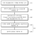
도1은 본 발명의 일 실시 예들에 따른 반도체 장치의 형성 방법을 설명하기 위한 순서도이다.
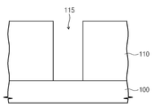
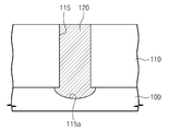
도2a 내지 도2d은 본 발명의 일 실시 예에 따른 반도체 장치의 형성 방법을 설명하기 위한 단면도들이다.
도3a 내지 도3j는 본 발명의 다른 일 실시 예들에 따른 반도체 장치의 형성 방법을 설명하기 위한 단면도들이다.
도4는 본 발명의 실시 예들에 따른 반도체 장치를 포함하는 메모리 시스템의 일 예를 간략히 도시한 블록도이다.
도5는 본 발명의 실시 예들에 따른 반도체 장치를 구비하는 메모리 카드의 일 예를 간략히 도시한 블록도이다.1 is a flowchart illustrating a method of forming a semiconductor device in accordance with one embodiment of the present invention.
2A through 2D are cross-sectional views illustrating a method of forming a semiconductor device in accordance with an embodiment of the present invention.
3A through 3J are cross-sectional views illustrating a method of forming a semiconductor device in accordance with some example embodiments of the present inventive concepts.
4 is a block diagram schematically illustrating an example of a memory system including a semiconductor device according to example embodiments of the inventive concepts.
5 is a block diagram schematically illustrating an example of a memory card including a semiconductor device according to example embodiments of the inventive concepts.
이상의 본 발명의 목적들, 다른 목적들, 특징들 및 이점들은 첨부된 도면과 관련된 이하의 바람직한 실시 예들을 통해서 쉽게 이해될 것이다. 그러나, 본 발명은 여기서 설명되는 실시 예들에 한정되지 않고 다른 형태로 구체화될 수도 있다. 오히려, 여기서 소개되는 실시 예는 개시된 내용이 철저하고 완전해질 수 있도록 그리고 당업자에게 본 발명의 사상이 충분히 전달될 수 있도록 하기 위해 제공되는 것이다.BRIEF DESCRIPTION OF THE DRAWINGS The above and other objects, features, and advantages of the present invention will become more readily apparent from the following description of preferred embodiments with reference to the accompanying drawings. However, the present invention is not limited to the embodiments described herein but may be embodied in other forms. Rather, the embodiments disclosed herein are provided so that this disclosure will be thorough and complete, and will fully convey the concept of the invention to those skilled in the art.
본 명세서에서 사용된 용어는 실시 예들을 설명하기 위한 것이며 본 발명을 제한하고자 하는 것은 아니다. 본 명세서에서, 단수형은 문구에서 특별히 언급하지 않는 한 복수형도 포함한다. 명세서에서 사용되는 '포함한다(comprises)' 및/또는 '포함하는(comprising)'은 언급된 구성요소, 단계, 동작 및/또는 소자는 하나 이상의 다른 구성요소, 단계, 동작 및/또는 소자의 존재 또는 추가를 배제하지 않는다. 본 명세서에서 어떤 막(또는 층)이 다른 막(또는 층) 또는 기판상에 있다고 언급되는 경우에 그것은 다른 막(또는 층) 또는 기판상에 직접 형성될 수 있거나 또는 그들 사이에 제 3의 막(또는 층)이 개재될 수도 있다. The terminology used herein is for the purpose of describing particular embodiments only and is not intended to be limiting of the invention. In the present specification, the singular form includes plural forms unless otherwise specified in the specification. As used herein, the terms 'comprises' and / or 'comprising' mean that the stated element, step, operation and / or element does not imply the presence of one or more other elements, steps, operations and / Or additions. Where it is mentioned herein that a film (or layer) is on another film (or layer) or substrate, it may be formed directly on another film (or layer) or substrate or a third film ( Or layers) may be interposed.
본 명세서에서 기술하는 실시 예들은 본 발명의 이상적인 예시도인 단면도 및/또는 평면도들을 참고하여 설명될 것이다. 도면들에 있어서, 구성들의 크기 및 두께 등은 명확성을 위하여 과장된 것이다. 따라서, 제조 기술 및/또는 허용 오차 등에 의해 예시도의 형태가 변형될 수 있다. 본 발명의 실시 예들은 도시된 특정 형태로 제한되는 것이 아니라 제조 공정에 따라 생성되는 형태의 변화도 포함하는 것이다. 예를 들면, 직각으로 도시된 식각 영역은 라운드 지거나 소정 곡률을 가지는 형태일 수 있다. 따라서, 도면에서 예시된 영역들은 개략적인 속성을 가지며, 도면에서 예시된 영역들의 모양은 소자의 영역의 특정 형태를 예시하기 위한 것이며 발명의 범주를 제한하기 위한 것이 아니다.Embodiments described herein will be described with reference to cross-sectional views and / or plan views, which are ideal illustrations of the invention. In the drawings, the size, thickness, etc. of the components are exaggerated for clarity. Accordingly, shapes of the exemplary views may be modified by manufacturing techniques and / or tolerances. Embodiments of the present invention are not limited to the specific forms shown, but also include changes in form generated by the manufacturing process. For example, the etched region shown at right angles may be rounded or have a predetermined curvature. Accordingly, the regions illustrated in the figures have schematic attributes, and the shape of the regions illustrated in the figures is intended to illustrate a particular form of region of the device and not to limit the scope of the invention.
본 명세서의 다양한 실시 예들에서 제1, 제2, 제3 등의 용어가 다양한 영역, 막들(또는 층들) 등을 기술하기 위해서 사용되었지만, 이들 영역, 막들이 이 같은 용어들에 의해서 한정되어서는 안 된다. 이들 용어들은 단지 어느 소정 영역 또는 막(또는 층)을 다른 영역 또는 막(또는 층)과 구별시키기 위해서 사용되었을 뿐이다. 따라서, 어느 한 실시 예에의 제1막질로 언급된 막질이 다른 실시 예에서는 제2막질로 언급될 수도 있다. 여기에 설명되고 예시되는 각 실시 예는 그것의 상보적인 실시 예도 포함한다. 명세서 전체에 걸쳐서 동일한 참조번호로 표시된 부분들은 동일한 구성요소들을 나타낸다.Although the terms first, second, third, etc. have been used in various embodiments herein to describe various regions, films (or layers), etc., it is to be understood that these regions, do. These terms are merely used to distinguish any given region or film (or layer) from another region or film (or layer). Therefore, the film quality referred to as the first film quality in one embodiment may be referred to as the second film quality in other embodiments. Each embodiment described and illustrated herein also includes its complementary embodiment. Portions denoted by like reference numerals denote like elements throughout the specification.
이하, 본 발명의 일 실시 예들에 따른 반도체 장치의 형성 방법이 설명된다. 도1은 본 발명의 일 실시 예들에 따른 반도체 장치의 형성 방법을 설명하기 위한 순서도이고, 도2a 내지 도2d은 본 발명의 일 실시 예에 따른 반도체 장치의 형성 방법을 설명하기 위한 단면도들이다.Hereinafter, a method of forming a semiconductor device according to one embodiment of the present invention will be described. 1 is a flowchart illustrating a method of forming a semiconductor device in accordance with one embodiment of the present invention, and FIGS. 2A to 2D are cross-sectional views illustrating a method of forming a semiconductor device in accordance with one embodiment of the present invention.
도1 및 도2a를 참조하면, 기판(100)상에 절연막(110)을 형성할 수 있다. 상기 절연막(110)은 물리 기상 증착 공정(Physical Vapor Deposition Process:PVD), 화학 기상 증착 공정(Chemical Vapor Deposition Process:CVD) 또는 원자층 증착 공정(Atomic Layer Deposition Process:ALD)에 의해 형성될 수 있다. 상기 절연막(110)은 단일층(Single-layered) 또는 다층(Multi-layered)으로 형성될 수 있다. 상기 절연막(110)은 산화물, 질화물 또는 산화질화물 중에서 적어도 하나를 포함할 수 있다. 상기 기판(100)은 반도체 물질을 포함할 수 있다. 예컨대, 상기 기판(100)은 실리콘 기판 또는 실리콘-게르마늄 기판 중에서 적어도 하나일 수 있다.1 and 2A, an
도1 및 도2b를 참조하면, 상기 절연막(110)내에 상기 절연막(110)을 관통하여 상기 기판(100)의 상부면을 노출시키는 개구부(115)를 형성할 수 있다(S10). 일 실시 예에 따르면, 상기 개구부(115)는 홀 형태 또는 라인 형태일 수 있다. 상기 개구부(115)를 형성하는 것은 상기 절연막(110)상에 마스크 패턴을 형성하는 것 및 상기 마스크 패턴을 식각 마스크로 이용하여 상기 절연막(110)을 식각하는 것을 포함할 수 있다. 1 and 2B, an
일 실시 예에 따르면, 상기 절연막(110)을 식각하는 것은 플라즈마를 이용하는 이방성 식각 공정에 의해 수행될 수 있다. 상기 이방성 식각 공정은 이방성 식각이 우세한 식각 공정일 수 있다. 상기 이방성 식각 공정이 플라즈마를 이용하므로, 상기 개구부(115)에 의해 노출되는 상기 기판(100)의 상부 영역 내에 플라즈마 손상 영역이 형성될 수 있다. 상기 플라즈마 손상 영역은 상기 이방성 식각 공정에서 사용된 플라즈마에 의해서 상기 기판(100)의 상부면에 반도체 원자들간의 결합이 깨진 영역일 수 있다. According to an embodiment, etching of the insulating
도1 및 도2c를 참조하면, 상기 개구부(115)에 의해 노출되는 상기 기판(100)의 상부 영역에 플라즈마-프리-식각 공정을 수행하여 상기 기판(100)내에 리세스 영역(115a)을 형성할 수 있다(S30). 상기 개구부(115)에 의해 노출되는 상기 기판(100)에 식각 가스를 이용하는 상기 플라즈마-프리-식각 공정을 수행하여 상기 기판(100)내에 리세스 영역(115a)를 형성할 수 있다. 상기 플라즈마-프리-식각 공정은 플라즈마를 사용하지 않고, 상기 개구부(115)에 의해 노출된 상기 기판(100)의 상부 영역과 상기 식각 가스를 반응시켜서 상기 기판(100)의 일부를 식각하는 것일 수 있다. 상기 플라즈마-프리-식각 공정은 플라즈마를 사용하지 않는 식각 공정이므로, 상기 플라즈마-프리-식각 공정에 의해 형성된 리세스 영역(115a)의 내면에 플라즈마 손상 영역이 형성되는 것을 최소화할 수 있다. 1 and 2C, a recessed
상기 식각 가스는 상기 기판(100)에 포함된 반도체 물질과 반응할 수 있는 가스들을 포함할 수 있다. 예를 들어, 상기 기판(100)이 실리콘을 포함하는 경우, 상기 식각 가스는 할로겐간 화합물(Interhalogen compound), 불소(F2) 및 불화 제논(XeF2) 중에서 적어도 하나를 포함할 수 있다. 예를 들어, 상기 할로겐간 화합물은 불소-브롬 화합물(ex, BrF, BrF3 또는 BrF5), 염소-불소 화합물(ex, ClF, ClF3 또는 ClF5) 또는 요오드-불소 화합물 (ex, IF3 또는 IF5) 중에서 적어도 하나일 수 있다. The etching gas may include gases that may react with the semiconductor material included in the
상기 식각 가스는 상기 기판(100)에 대해서 높은 식각 선택성을 가질 수 있다. 즉, 상기 기판(100)의 상기 식각 가스에 의한 식각률은 상기 절연막(110)의 상기 식각 가스에 의한 식각률보다 높을 수 있다. 예를 들어, 상기 기판(100)이 실리콘을 포함하고, 상기 절연막(110)이 실리콘 산화물을 포함하는 경우, 상기 식각 가스에 의한 상기 기판(100)의 식각률은 상기 식각 가스에 의한 상기 절연막(110)의 식각률보다 100배 이상 클 수 있다. 또한, 상기 기판(100)이 실리콘을 포함하고, 상기 절연막(110)이 실리콘 질화물을 포함하는 경우, 상기 식각 가스에 의한 상기 기판(100)의 식각률은 상기 식각 가스에 의한 상기 절연막(110)의 식각률보다 50배 이상 클 수 있다. 따라서, 상기 플라즈마-프리-식각 공정에서 상기 절연막(110)이 식각되는 것을 최소화할 수 있다.The etching gas may have high etching selectivity with respect to the
일 실시 예에 따르면, 상기 플라즈마-프리-식각 공정은 상온~300℃의 공정 온도 및 0.00001~1atm의 공정 압력에서 수행될 수 있다. 일 실시 예에 따르면, 상기 식각 가스는 불활성 가스를 더 포함할 수 있다. 예를 들어, 상기 식각 가스는 질소 또는 아르곤 중에서 적어도 하나를 포함할 수 있다.According to one embodiment, the plasma-pre-etching process may be performed at a process temperature of room temperature ~ 300 ℃ and a process pressure of 0.00001 ~ 1 atm. According to an embodiment, the etching gas may further include an inert gas. For example, the etching gas may include at least one of nitrogen or argon.
상기 플라즈마-프리-식각 공정은 등방성 식각 공정일 수 있다. 상기 등방성 식각 공정에 의해서 상기 리세스 영역(115a)은 상기 개구부(115)의 측벽을 지나서 옆으로 연장된 형태일 수 있다. 즉, 상기 리세스 영역(115a)의 최장폭은 상기 개구부(115)의 하단의 폭보다 길수 있다.The plasma-pre-etch process may be an isotropic etching process. The
상기 플라즈마-프리-식각 공정을 수행하기 전에, 상기 개구부(115)에 의해 노출되는 상기 기판(100)의 상부면에 형성된 자연 산화막을 제거하기 위한 전식각 공정(Pre-Etching Process)을 수행할 수 있다(S20).Before performing the plasma-pre-etching process, a pre-etching process may be performed to remove the native oxide film formed on the upper surface of the
상기 개구부(115)를 형성한 후, 상기 개구부(115)에 의해 노출된 기판(100)의 상부면에 자연 산화막이 형성될 수 있다. 상기 전식각 공정은 공정 가스를 이용하여 상기 기판(100)의 상부면의 자연 산화막을 제거할 수 있다. 상기 전식각 공정은 플라즈마를 사용하지 않고, 상기 기판(100)의 상부면의 자연 산화막과 상기 공정 가스를 반응시켜서 상기 자연 산화막을 제거하는 것일 수 있다. 상기 전식각 공정은 플라즈마를 사용하지 않는 식각 공정이므로, 상기 전식각 공정이 수행된 기판의 표면에 플라즈마 손상 영역이 형성되는 것을 최소화할 수 있다.After the
상기 공정 가스는 상기 자연 산화막에 포함된 산화물과 반응할 수 있는 가스들을 포함할 수 있다. 예를 들어, 상기 자연 산화막이 실리콘 산화물을 포함하는 경우, 상기 공정 가스는 암모니아, 불화 수소 또는 불화 질소 중에서 적어도 하나를 포함할 수 있다. 일 실시 예에 따르면, 상기 전식각 공정은 상온~300℃의 공정 온도 및 0.00001~1atm의 공정 압력에서 수행될 수 있다. 일 실시 예에 따르면, 상기 공정 가스는 불활성 가스를 더 포함할 수 있다. 예를 들어, 상기 식각 가스는 질소 또는 아르곤 중에서 적어도 하나를 포함할 수 있다.The process gas may include gases capable of reacting with an oxide included in the natural oxide film. For example, when the natural oxide film includes silicon oxide, the process gas may include at least one of ammonia, hydrogen fluoride, or nitrogen fluoride. According to one embodiment, the pre-etching process may be performed at a process temperature of room temperature ~ 300 ℃ and a process pressure of 0.00001 ~ 1 atm. According to one embodiment, the process gas may further include an inert gas. For example, the etching gas may include at least one of nitrogen or argon.
일 실시 예에 따르면, 상기 전식각 공정은 등방성 식각 공정일 수 있다. 따라서, 상기 전식각 공정에서 상기 개구부(115)의 내측벽이 옆으로 식각될 수 있다. 상기 전식각 공정에서 사용되는 공정 가스가 상기 개구부(115)에 의해 노출된 상기 절연막(110)과 반응하여 식각되는 것에 의해서 상기 개구부(115)의 폭이 증가될 수 있다.According to one embodiment, the pre-etching process may be an isotropic etching process. Therefore, the inner wall of the
상기 리세스 영역(115a)이 형성된 기판(100)에 수소 치환 공정을 더 수행할 수 있다(S40). 상기 수소 치환 공정은 상기 리세스 영역(115a)의 내면에 수소를 포함하는 가스를 제공하는 것(S42) 및 상기 기판(100)에 열처리 공정을 수행하는 것(S44)을 포함할 수 있다. 수소를 포함한 가스는 불화 수소 또는 암모니아 중에서 적어도 하나를 포함할 수 있다. 상기 열처리 공정은 150~250℃에서 수행될 수 있다.A hydrogen substitution process may be further performed on the
상기 리세스 영역(115a)내에 상기 플라즈마-프리-식각 공정에서 사용된 식각 가스 포함된 할로겐 원소와 상기 리세스 영역(115a)의 내면의 반도체 원소가 결합된 반도체-할로겐 결합물이 형성될 수 있다. 상기 수소 치환 공정은 상기 반도체-할로겐 결합물을 반도체-수소 결합물로 변경할 수 있다. In the
상기 수소 치환 공정에 의해서 상기 리세스 영역(115a)의 내면에 반도체-할로겐 결합물보다 결합력이 강한 반도체-수소 결합물이 형성되어 상기 리세스 영역(115a) 내면에 자연 산화막이 형성되는 것을 최소화할 수 있다.The hydrogen substitution process forms a semiconductor-hydrogen bond having a stronger bonding force than the semiconductor-halogen bond on the inner surface of the
도2d를 참조하면, 상기 개구부(115) 및 상기 리세스 영역(115a) 내에 도전체(120)를 형성할 수 있다. 상기 도전체(120)는 반도체 물질(ex, 다결정 실리콘), 금속-반도체 화합물(ex, 텅스텐 실리사이드), 도전성 금속질화물(ex, 티타늄 질화물, 탄탈늄 질화물 또는 텅스텐 질화물 등) 또는 금속(ex, 티타늄, 텅스텐 또는 탄탈늄 등) 중에서 선택된 적어도 하나를 포함할 수 있다. 일 실시 예에 따르면, 상기 도전체(120)는 상기 개구부(115) 및 상기 리세스 영역(115a)의 내면과 접촉할 수 있다.Referring to FIG. 2D, a
상기 도전체(120)를 형성하는 것은 상기 절연막(110)상에 상기 개구부(115) 및 상기 리세스 영역(115a)을 채우는 도전막을 형성하는 것 및 상기 도전막을 상기 절연막(110)의 상부면이 노출될 때까지 식각하는 것을 포함할 수 있다. 상기 도전막은 화학 기상 증착 공정 또는 물리 기상 증착 공정에 의해 형성될 수 있다. 상기 식각 공정은 에치백 공정 또는 화학적 기계적 평탄화 공정 중에서 적어도 하나에 의해 수행될 수 있다. The
본 발명의 일 실시 예들에 따르면, 상기 개구부(115)를 형성한 후, 플라즈마를 사용하지 않는 플라즈마-프리-식각 공정에 의해 리세스 영역(115a)이 형성될 수 있다. 따라서, 상기 리세스 영역(115a)의 내면에 플라즈마 손상 영역이 형성되는 것을 최소화할 수 있다. 만약, 상기 리세스 영역이 플라즈마를 이용하는 이방성 식각 공정에 의해 형성된다면, 상기 리세스 영역의 내면에 반도체 원자들간의 결합이 깨진 플라즈마 손상 영역이 형성될 수 있다. 따라서, 상기 리세스 영역 내에 형성되는 도전체의 저항을 증가시킬 수 있다. 하지만, 본 발명의 일 실시 예들에 따르면, 상기 리세스 영역(115a)의 내면에 플라즈마 손상 영역이 형성되는 것을 최소화할 수 있으므로, 상기 개구부(115) 및 상기 리세스 영역(115a) 내에 형성되는 도전체(120)의 저항을 감소시킬 수 있다. 결과적으로, 신뢰성 및 전기적 특성이 개선된 반도체 장치를 구현할 수 있다.According to one embodiment of the present invention, after the
이에 더하여, 상기 리세스 영역(115a)이 상기 개구부(115)의 측벽을 지나서 옆으로 연장된 형태인 경우, 상기 리세스 영역(115a) 및 상기 개구부(115) 내에 형성되는 도전체(120)가 상기 기판(100)과 접촉하는 면적이 증가될 수 있다. 상기 도전체(120)와 상기 기판(100)의 접촉 면적의 증가에 의해서 상기 도전체(120)의 저항을 감소시킬 수 있다. 따라서, 신뢰성 및 전기적 특성이 개선된 반도체 장치를 구현할 수 있다.In addition, when the
상술된 실시 예들에 따른 반도체 장치의 형성 방법은 반도체 장치의 제조 과정에서 다양하게 적용될 수 있다. 이하, 본 발명의 실시 예들에 따른 반도체 기억 장치의 형성 방법에 대해서 도면을 참조하여 설명한다. 도3a 내지 도3j는 본 발명의 다른 일 실시 예들에 따른 반도체 장치의 형성 방법을 설명하기 위한 단면도들이다.The method of forming the semiconductor device according to the above-described embodiments may be variously applied in the manufacturing process of the semiconductor device. Hereinafter, a method of forming a semiconductor memory device according to embodiments of the present invention will be described with reference to the drawings. 3A through 3J are cross-sectional views illustrating a method of forming a semiconductor device in accordance with some example embodiments of the present inventive concepts.
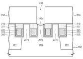
도3a를 참조하면, 활성부(203)을 정의하는 소자 분리 패턴(201)을 포함하는 기판(200)이 준비된다. 상기 소자 분리 패턴(201)은 절연 물질을 포함할 수 있다. 예컨대, 상기 소자 분리 패턴(201)은 산화물, 질화물 또는 산화질화물을 중에서 적어도 하나를 포함할 수 있다. 상기 기판(200)은 반도체 물질을 포함할 수 있다. 예컨대, 상기 기판(200)은 실리콘 또는 게르마늄 중에서 적어도 하나를 포함할 수 있다.Referring to FIG. 3A, a
상기 기판(200)내에 트렌치(205)를 형성할 수 있다. 도시되지는 않았지만, 상기 트렌치(205)는 평면적 관점에서 일 방향으로 연장되고, 상기 활성부(203) 및 상기 소자 분리 패턴(201)을 가로지르는 라인 형태로 형성될 수 있다. 일 실시 예에 따르면, 상기 기판(200)에 복수의 트렌치(205)들이 형성될 수 있다. 예를 들어, 한 쌍의 트렌치들(205)이 상기 활성부(203)를 가로지를 수 있다.A
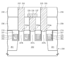
상기 각 트렌치(205)내에 게이트 전극이 형성될 수 있다. 상기 게이트 전극은 벌크 게이트 패턴(225) 및 라이너 게이트 패턴(223)을 포함할 수 있다. 상기 벌크 게이트 패턴(225)은 상기 트렌치(205)내에 배치되도록 형성될 수 있다. 상기 라이너 게이트 패턴(223)은 상기 벌크 게이트 패턴(225)과 상기 트렌치(205)사이에 배치되도록 형성될 수 있다. 상기 라이너 게이트 패턴(223) 및 상기 벌크 게이트 패턴(225)은 도핑된 반도체, 도전성 금속질화물(ex, 티타늄 질화물, 탄탈늄 질화물 또는 텅스텐 질화물 등) 또는 금속(ex, 루세늄, 이리듐, 티타늄, 텅스텐 또는 탄탈늄 등) 중에서 선택된 적어도 하나를 포함할 수 있다. 일 실시 예에 따르면, 상기 벌크 게이트 패턴(225)과 상기 라이너 게이트 패턴(223)은 서로 다른 도전 물질을 포함할 수 있다. 예를 들어, 상기 벌크 게이트 패턴(225)은 텅스텐을 포함하고, 상기 라이너 게이트 패턴(223)은 티타늄 질화물을 포함할 수 있다.A gate electrode may be formed in each of the
상기 트렌치(205)와 상기 라이너 게이트 패턴(223)사이에 게이트 유전막(210)이 형성될 수 있다. 상기 게이트 유전막(210)은 상기 트렌치의 내면을 따라 연장될 수 있으며, 상기 기판(200)의 상부면을 덮을 수 있다. 상기 게이트 유전막(210)은 고 유전물질, 산화물, 질화물 또는 산화 질화물 중에서 선택된 적어도 하나를 포함할 수 있다. 상기 고유전 물질은 질화물의 유전상수에 비하여 높은 유전상수를 갖는 절연물질일 수 있다. 예컨대, 상기 고유전 물질은 산화 하프늄 또는 산화알루미늄등과 같은 절연성 금속산화물 중에서 선택된 적어도 하나일 수 있다.A
상기 트렌치(205)내의 상기 게이트 전극 상에 캐핑 패턴(227)이 배치될 수 있다. 상기 캐핑 패턴(227)은 상기 게이트 전극의 상부면을 덮도록 형성될 수 있다. 상기 캐핑 패턴(227)은 절연 물질을 포함할 수 있다. 예컨대, 상기 캐핑 패턴(227)은 산화물, 질화물 또는 산화질화물 중에서 적어도 선택된 적어도 하나를 포함할 수 있다.A
상기 트렌치들(205) 양측의 상기 활성부(203) 내에 상기 트렌치(205)와 인접한 도핑 영역들(207a, 207b)을 형성할 수 있다. 일 실시 예에 따르면, 상기 활성부(203)내에 제1 도핑 영역(207a) 및 한 쌍의 제2 도핑 영역들(207b)이 형성될 수 있다. 상기 제1 도핑 영역(207a)은 상기 한 쌍의 게이트 전극들 사이의 활성부(203)내에 형성될 수 있다. 또한, 상기 한 쌍의 제2 도핑 영역들(207b) 사이에 상기 한 쌍의 게이트 전극들 및 상기 제1 도핑 영역(207a)이 배치되도록 형성될 수 있다.
상기 도핑 영역들(207a, 207b)의 하부면은 상기 활성부(203)의 상부면으로부터 소정의 깊이에 형성될 수 있다. 상기 도핑 영역들(207a, 207b)은 상기 트렌치들(205)의 측벽에 접할 수 있다. 상기 도핑 영역들(207a, 207b)은 상기 활성부(203)내에 불순물을 주입하는 공정에 의해서 형성될 수 있다. 일 실시 예에 따르면, 상기 도핑 영역들(207a, 207b)의 하부면은 상기 각 트렌치(205)의 바닥면보다 높을 수 있다.Lower surfaces of the doped
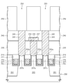
상기 기판(200)상에 제1 층간 절연막(230)을 형성할 수 있다. 상기 제1 층간 절연막(230)은 물리 기상 증착 공정(PVD), 화학 기상 증착 공정(CVD) 또는 원자층 증착 공정(ALD)에 의해 형성될 수 있다. 상기 제1 층간 절연막(230)은 산화물, 질화물 또는 산화질화물 중에서 선택된 적어도 하나를 포함할 수 있다. A first
상기 제1 층간 절연막(230)내에 상기 제1 층간 절연막(230)을 관통하여 상기 활성부(203)의 제1 도핑 영역(207a)을 노출시키는 제1 홀(233)을 형성할 수 있다. 상기 제1 홀(233)은 상기 제1 층간 절연막(230) 상에 제1 마스크 패턴을 형성하고, 상기 제1 마스크 패턴을 이용하여 상기 제1 층간 절연막(230)을 식각 하는 것에 의해 형성될 수 있다.A
일 실시 예에 따르면, 상기 제1 층간 절연막(230)을 식각하는 것은 플라즈마를 이용하는 제1 이방성 식각 공정에 의해 수행될 수 있다. 상기 이방성 식각 공정이 플라즈마를 이용하므로, 제1 홀(233)에 의해 노출되는 상기 제1 도핑 영역(207a)의 상부 영역 내에 플라즈마 손상 영역이 형성될 수 있다. 상기 플라즈마 손상 영역은 상기 이방성 식각 공정에서 사용된 플라즈마에 의해서 상기 제1 도핑 영역(207a)의 상부 영역 내의 반도체 원자들간의 결합이 깨진 영역일 수 있다.In example embodiments, the etching of the first
도3b를 참조하면, 상기 제1 홀(233)에 의해 노출되는 상기 활성부(203)의 상부 영역에 제1 플라즈마-프리-식각 공정을 수행하여 상기 활성부(203)내에 제1 리세스 영역(233a)을 형성할 수 있다.Referring to FIG. 3B, a first recess region is formed in the
상기 제1 홀(233)에 의해 노출되는 상기 제1 도핑 영역(207a)에 제1 식각 가스를 이용하는 상기 제1 플라즈마-프리-식각 공정을 수행하여 상기 제1 도핑 영역(207a)내에 제1 리세스 영역(233a)를 형성할 수 있다. 상기 제1 플라즈마-프리-식각 공정은 플라즈마를 사용하지 않고, 상기 제1 홀(233)에 의해 노출된 상기 제1 도핑 영역(207a)의 상부 영역과 상기 제1 식각 가스를 반응시켜서 상기 제1 도핑 영역(207a)의 일부를 식각하는 것일 수 있다. 상기 제1 플라즈마-프리-식각 공정은 플라즈마를 사용하지 않는 식각 공정이므로, 상기 제1 플라즈마-프리-식각 공정에 의해 형성된 제1 리세스 영역(233a)의 내면에 플라즈마 손상 영역이 형성되는 것을 최소화할 수 있다. A first lith in the first
상기 제1 식각 가스는 상기 제1 도핑 영역(207a)에 포함된 반도체 원소와 반응할 수 있는 가스들을 포함할 수 있다. 예를 들어, 상기 제1 도핑 영역(207a)이 실리콘을 포함하는 경우, 상기 제1 식각 가스는 할로겐간 화합물(Interhalogen compound), 불소(F2) 및 불화 제논(XeF2) 중에서 적어도 하나를 포함할 수 있다. 예를 들어, 상기 할로겐간 화합물은 불소-브롬 화합물(ex, BrF, BrF3 또는 BrF5), 염소-불소 화합물(ex, ClF, ClF3 또는 ClF5) 또는 요오드-불소 화합물 (ex, IF3 또는 IF5) 중에서 적어도 하나일 수 있다. The first etching gas may include gases that may react with the semiconductor element included in the first
상기 제1 식각 가스는 상기 제1 도핑 영역(207a)에 대해서 높은 식각 선택성을 가질 수 있다. 즉, 상기 제1 도핑 영역(207a)의 상기 제1 식각 가스에 의한 식각률은 상기 제1 층간 절연막(230)의 상기 제1 식각 가스에 의한 식각률보다 높을 수 있다. 예를 들어, 상기 제1 도핑 영역(207a)이 실리콘을 포함하고, 상기 제1 층간 절연막(230)이 실리콘 산화물을 포함하는 경우, 상기 제1 식각 가스에 의한 상기 제1 도핑 영역(207a)의 식각률은 상기 제1 식각 가스에 의한 상기 제1 층간 절연막(230)의 식각률보다 100배 이상 클 수 있다. 또한, 상기 제1 도핑 영역(207a)이 실리콘을 포함하고, 상기 제1 층간 절연막(230)이 실리콘 질화물을 포함하는 경우, 상기 제1 식각 가스에 의한 상기 제1 도핑 영역(207a)의 식각률은 상기 제1 식각 가스에 의한 상기 제1 층간 절연막(230)의 식각률보다 50배 이상 클 수 있다. 즉, 상기 제1 플라즈마-프리-식각 공정에서 상기 활성부(203)의 제1 도핑 영역(207a)만을 선택적으로 식각할 수 있다. 따라서, 상기 제1 플라즈마-프리-식각 공정에서 상기 제1 층간 절연막(230)이 식각되는 것을 최소화할 수 있다. The first etching gas may have high etching selectivity with respect to the first
일 실시 예에 따르면, 상기 제1 플라즈마-프리-식각 공정은 상온~300℃의 공정 온도 및 0.00001~1atm의 공정 압력에서 수행될 수 있다. 일 실시 예에 따르면, 상기 제1 식각 가스는 불활성 가스를 더 포함할 수 있다. 예를 들어, 상기 제1 식각 가스는 질소 또는 아르곤 중에서 적어도 하나를 포함할 수 있다.According to an embodiment, the first plasma-pre-etching process may be performed at a process temperature of room temperature to 300 ° C. and a process pressure of 0.00001 to 1 atm. According to one embodiment, the first etching gas may further include an inert gas. For example, the first etching gas may include at least one of nitrogen or argon.
상기 제1 플라즈마-프리-식각 공정을 수행하기 전에, 상기 제1 홀(233)에 의해 노출되는 상기 제1 도핑 영역(207a)의 상부면에 형성된 자연 산화막을 제거하기 위한 제1 전식각 공정을 수행할 수 있다.Before performing the first plasma-pre-etch process, a first pre-etch process for removing the native oxide film formed on the upper surface of the first
상기 제1 홀(233)을 형성한 후, 상기 제1 홀(233)에 의해 노출된 상기 제1 도핑 영역(207a)의 상부면에 자연 산화막이 형성될 수 있다. 상기 제1 전식각 공정은 공정 가스를 이용하여 상기 제1 도핑 영역(207a)의 상부면의 자연 산화막을 제거할 수 있다. 상기 제1 전식각 공정은 플라즈마를 사용하지 않고, 상기 제1 도핑 영역(207a)의 상부면의 자연 산화막과 상기 공정 가스를 반응시켜서 상기 자연 산화막을 제거하는 것일 수 있다. 상기 제1 전식각 공정은 플라즈마를 사용하지 않는 식각 공정이므로, 상기 제1 전식각 공정이 수행된 상기 제1 도핑 영역(207a)의 표면에 플라즈마 손상 영역이 형성되는 것을 최소화할 수 있다.After forming the
상기 공정 가스는 상기 자연 산화막에 포함된 산화물과 반응할 수 있는 가스들을 포함할 수 있다. 예를 들어, 상기 자연 산화막이 실리콘 산화물을 포함하는 경우, 상기 공정 가스는 암모니아, 불화 수소 또는 불화 질소 중에서 적어도 하나를 포함할 수 있다. The process gas may include gases capable of reacting with an oxide included in the natural oxide film. For example, when the natural oxide film includes silicon oxide, the process gas may include at least one of ammonia, hydrogen fluoride, or nitrogen fluoride.
일 실시 예에 따르면, 상기 제1 전식각 공정은 상온~300℃의 공정 온도 및 0.00001~1atm의 공정 압력에서 수행될 수 있다. 일 실시 예에 따르면, 상기 공정 가스는 불활성 가스를 더 포함할 수 있다. 예를 들어, 상기 식각 가스는 질소 또는 아르곤 중에서 적어도 하나를 포함할 수 있다.According to one embodiment, the first pre-etching process may be performed at a process temperature of room temperature ~ 300 ℃ and a process pressure of 0.00001 ~ 1 atm. According to one embodiment, the process gas may further include an inert gas. For example, the etching gas may include at least one of nitrogen or argon.
일 실시 예에 따르면, 상기 제1 전식각 공정은 등방성 식각 공정일 수 있다. 따라서, 상기 제1 전식각 공정에 의해서 상기 제1 홀(233)의 내측벽이 옆으로 식각될 수 있다. 상기 제1 전식각 공정에서 사용되는 공정 가스가 상기 제1 홀(233)에 의해 노출된 상기 제1 층간 절연막(230)과 반응하여 식각되는 것에 의해서 상기 제1 홀(233)의 폭이 증가될 수 있다.According to one embodiment, the first pre-etching process may be an isotropic etching process. Therefore, the inner wall of the
상기 제1 리세스 영역(233a)이 형성된 기판(200)에 제1 수소 치환 공정을 더 수행할 수 있다. 상기 제1 수소 치환 공정은 상기 제1 리세스 영역(233a)의 내면에 수소를 포함하는 가스를 제공하는 것 및 상기 기판(200)에 열처리 공정을 수행하는 것을 포함할 수 있다. 상기 수소를 포함한 가스는 불화 수소 또는 암모니아 중에서 적어도 하나를 포함할 수 있다. 상기 열처리 공정은 150~250℃에서 수행될 수 있다. A first hydrogen substitution process may be further performed on the
상기 제1 리세스 영역(233a)내에 상기 제1 플라즈마-프리-식각 공정에서 사용된 제1 식각 가스 포함된 할로겐 원소와 상기 제1 리세스 영역(233a)의 내면의 반도체 원소가 결합된 반도체-할로겐 결합물이 형성될 수 있다. 상기 제1 수소 치환 공정은 상기 반도체-할로겐 결합물을 반도체-수소 결합물로 변경할 수 있다. A semiconductor in which a halogen element included in a first etching gas used in the first plasma-pre-etch process and a semiconductor element of an inner surface of the
상기 제1 수소 치환 공정에 의해서 상기 제1 리세스 영역(233a)의 내면에 상기 반도체-할로겐 결합물보다 결합력이 강한 반도체-수소 결합물이 형성되어 상기 제1 리세스 영역(233a)의 내면에 자연 산화막이 형성되는 것을 최소화할 수 있다.By the first hydrogen substitution process, a semiconductor-hydrogen bond having a stronger bonding force than the semiconductor-halogen bond is formed on the inner surface of the
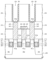
도3c를 참조하면, 상기 제1 홀(233) 및 상기 제1 리세스 영역(233a)내에 제1 콘택 플러그(235)를 형성할 수 있다. 상기 제1 콘택 플러그(235)는 반도체 물질(ex, 다결정 실리콘), 금속-반도체 화합물(ex, 텅스텐 실리사이드), 도전성 금속질화물(ex, 티타늄 질화물, 탄탈늄 질화물 또는 텅스텐 질화물 등) 또는 금속(ex, 티타늄, 텅스텐 또는 탄탈늄 등) 중에서 선택된 적어도 하나를 포함할 수 있다. 일 실시 예에 따르면, 상기 제1 콘택 플러그(235)는 상기 제1 홀(233) 및 상기 제1 리세스 영역(233a)의 내면과 접촉할 수 있다.Referring to FIG. 3C, a
본 발명의 일 실시 예들에 따르면, 상기 제1 홀(233)을 형성한 후, 플라즈마를 사용하지 않는 제1 플라즈마-프리-식각 공정에 의해 제1 리세스 영역(233a)이 형성될 수 있다. 따라서, 상기 제1 리세스 영역(233a)의 내면에 플라즈마 손상 영역이 형성되는 것을 최소화할 수 있다. 만약, 상기 리세스 영역이 플라즈마를 이용하는 이방성 식각 공정에 의해 형성된다면, 상기 리세스 영역의 내면에 플라즈마 손상 영역이 형성될 수 있다. 따라서, 상기 리세스 영역내에 형성되는 도전체의 저항을 증가시킬 수 있다. 하지만, 본 발명의 일 실시 예들에 따르면, 상기 제1 리세스 영역(233a)의 내면에 플라즈마 손상 영역이 형성되는 것을 최소화할 수 있으므로, 상기 리세스 영역(233a)과 제1 콘택 플러그(235)의 계면 저항을 감소시킬 수 있다. 따라서, 신뢰성 및 전기적 특성이 개선된 반도체 기억 장치를 구현할 수 있다.According to one embodiment of the present invention, after the
상기 제1 층간 절연막(230)상에 상기 제1 콘택 플러그(235)와 전기적으로 연결되는 배선(237)을 형성할 수 있다. 도시되지는 않았지만, 상기 배선(237)은 평면적 관점에서 상기 트렌치(205)가 연장되는 일 방향에 교차하는 방향으로 연장되는 라인 형태일 수 있다. 상기 배선(237)은 반도체 물질(ex, 다결정 실리콘), 금속-반도체 화합물(ex, 텅스텐 실리사이드), 도전성 금속질화물(ex, 티타늄 질화물, 탄탈늄 질화물 또는 텅스텐 질화물 등) 또는 금속(ex, 티타늄, 텅스텐 또는 탄탈늄 등) 중에서 선택된 적어도 하나를 포함할 수 있다. 상기 배선(237)은 상기 제1 층간 절연막(150)상에 도전막을 형성하고, 상기 도전막을 패터닝하는 것에 의해서 형성될 수 있다. 이와 달리, 상기 배선(237)은 다마신 공정(Damascene Process)에 의해 형성될 수 있다. 즉, 상기 배선(237)은 상기 제1 층간 절연막(230)상에 개구부가 포함된 절연막을 형성하고, 상기 개구부를 도전 물질로 채우는 것에 의해서 형성될 수 있다.A
상기 제1 층간 절연막(230)에 상기 배선(237)을 덮는 제2 층간 유전막(240)이 형성될 수 있다. 상기 제2 층간 유전막(240)은 화학 기상 증착 공정에 의해서 형성될 수 있다. 상기 제2 층간 유전막(240)은 산화물, 질화물 또는 산화질화물 중에서 선택된 적어도 하나를 포함할 수 있다. A second
도3d를 참조하면, 상기 제1 층간 절연막(230) 및 상기 제2 층간 유전막(240) 내에, 상기 제1 층간 절연막(230) 및 상기 제2 층간 유전막(240)을 관통하여 상기 활성부(203)의 상기 제2 도핑 영역들(207b)을 노출시키는 제2 홀(243)을 형성할 수 있다. 상기 제2 홀(243)은 상기 제2 층간 유전막(240)상에 제2 마스크 패턴을 형성하고, 상기 제2 마스크 패턴을 이용하여 상기 제1 층간 절연막(230) 및 상기 제2 층간 유전막(240)을 식각하는 것에 의해 형성될 수 있다.Referring to FIG. 3D, the
일 실시 예에 따르면, 상기 제1 층간 절연막(230) 및 상기 제2 층간 유전막(240)을 식각하는 것은 플라즈마를 이용하는 제2 이방성 식각 공정에 의해 수행될 수 있다. 상기 제2 이방성 식각 공정이 플라즈마를 이용하므로, 상기 제2 홀(243)에 의해 노출되는 상기 활성부(203)의 제2 도핑 영역들(207b)의 상부면에 플라즈마 손상 영역이 형성될 수 있다. 상기 플라즈마 손상 영역은 상기 제2 이방성 식각 공정에서 사용된 플라즈마에 의해서 상기 제2 도핑 영역들(207b)의 상부면의 반도체 원자들간의 결합이 깨진 영역일 수 있다. According to an embodiment, etching the first
도3e를 참조하면, 상기 제2 홀(243)에 의해 노출되는 상기 제2 도핑 영역들(207b)의 상부면에 제2 플라즈마-프리-식각 공정을 수행하여 상기 제2 도핑 영역들(207b)내에 제2 리세스 영역(243a)을 형성할 수 있다. 상기 제2 플라즈마-프리-식각 공정은 제2 식각 가스를 이용하여 상기 제2 도핑 영역들(207b)의 일부를 식각할 수 있다. 상기 제2 플라즈마-프리-식각 공정은 도3b를 참조하여 설명한 제1 리세스 영역(233a)을 형성하기 위한 제1 플라즈마-프리-식각 공정과 동일한 것일 수 있다. 또한, 상기 제2 식각 가스는 도3b를 참조하여 설명한 제1 식각 가스와 동일한 특성을 가질 수 있다. 따라서, 상기 제2 리세스 영역(243a)은 도3b를 참조하여 설명한 제1 리세스 영역(233a)과 동일한 특성을 가질 수 있다.Referring to FIG. 3E, a second plasma-pre-etch process is performed on an upper surface of the second
상기 제2 플라즈마-프리-식각 공정을 수행하기 전에, 상기 제2 홀(243)에 의해 노출되는 상기 제2 도핑 영역들(207b)의 상부면의 자연 산화막을 제거하기 위한 제2 전식각 공정을 수행할 수 있다. 상기 제2 전식각 공정은 상기 도3b를 참조하여 설명한 제1 전식각 공정과 동일한 것일 수 있다. 따라서, 상기 제2 전식각 공정은 상기 제1 전식각 공정과 동일한 가스 공정 가스를 사용할 수 있다.Before performing the second plasma-pre-etching process, a second pre-etching process for removing the native oxide film on the upper surface of the second
상기 제2 리세스 영역(243a)의 내면에 제2 수소 치환 공정을 더 수행할 수 있다. 상기 제2 수소 치환 공정은 도3를 참조하여 설명한 제1 수소 치환 공정과 동일한 것일 수 있다. 따라서, 상기 제2 수소 치환 공정은 상기 제2 리세스 영역(243a)의 내면에 수소를 포함하는 가스를 제공하는 것 및 상기 기판(200)에 열처리 공정을 수행하는 것을 포함할 수 있다.A second hydrogen substitution process may be further performed on the inner surface of the
상기 제2 수소 치환 공정에 의해서 상기 제2 리세스 영역(243a)의 내면에 상기 반도체-할로겐 결합물보다 결합력이 강한 반도체-수소 결합물이 형성되어 상기 제2 리세스 영역(243a)의 내면에 자연 산화막이 형성되는 것을 최소화할 수 있다.By the second hydrogen substitution process, a semiconductor-hydrogen bond having a stronger bonding force than that of the semiconductor-halogen bond is formed on the inner surface of the
도3f를 참조하면, 상기 제2 홀(243) 및 상기 제2 리세스 영역(243a)내에 제2 콘택 플러그(245)가 형성될 수 있다. 상기 제2 콘택 플러그(245)는 반도체 물질(ex, 다결정 실리콘), 금속-반도체 화합물(ex, 텅스텐 실리사이드), 도전성 금속질화물(ex, 티타늄 질화물, 탄탈늄 질화물 또는 텅스텐 질화물 등) 또는 금속(ex, 티타늄, 텅스텐 또는 탄탈늄 등) 중에서 선택된 적어도 하나를 포함할 수 있다. 일 실시 예에 따르면, 상기 제2 콘택 플러그(245)는 상기 제2 홀(243) 및 상기 제2 리세스 영역(243a)의 내면과 접촉할 수 있다.Referring to FIG. 3F, a
본 발명의 일 실시 예들에 따르면, 상기 제2 리세스 영역(243a)은 도3b를 참조하여 설명한 제1 리세스 영역(233a)과 동일한 특성을 가질 수 있고, 동일한 방법에 의해 형성될 수 있다. 따라서, 상기 제2 리세스 영역(243a)의 내면에 플라즈마 손상 영역이 형성되는 것을 최소화할 수 있으므로, 상기 제2 홀(243) 및 상기 제2 리세스 영역(243a)내에 형성되는 제2 콘택 플러그(245)의 저항을 감소시킬 수 있다. 결과적으로, 신뢰성 및 전기적 특성이 개선된 반도체 기억 장치를 구현할 수 있다.According to one embodiment of the present invention, the
도3g를 참조하면, 상기 제2 층간 유전막(240)상에 희생막(250)을 형성할 수 있다. 상기 희생막(250)내에 상기 제2 콘택 플러그(245)를 노출시키는 제3 홀(253)을 형성할 수 있다. 상기 제3 홀(253)을 형성하는 것은 상기 희생막(250)상에 제3 마스크 패턴을 형성하는 것 및 상기 제3 마스크 패턴을 식각 마스크로 이용하여 상기 희생막(250)을 식각하는 것을 포함할 수 있다. Referring to FIG. 3G, a
일 실시 예에 따르면, 상기 희생막(250)을 식각하는 것은 플라즈마를 이용하는 제3 이방성 식각 공정에 의해 수행될 수 있다. 일 실시 예에 따르면, 상기 제3 이방성 식각 공정에 의해서 상기 희생막(250)은 이방성으로 식각될 수 있다. 상기 제3 이방성 식각 공정이 플라즈마를 이용하므로, 상기 제3 홀(253)에 의해 노출되는 상기 제2 콘택 플러그(245)의 상부 영역 내에 플라즈마 손상 영역이 형성될 수 있다. 상기 플라즈마 손상 영역은 상기 제3 이방성 식각 공정에서 사용된 플라즈마에 의해서 상기 제2 콘택 플러그(245)의 상부 영역 내의 원자들간의 결합이 깨진 영역일 수 있다.In example embodiments, the etching of the
도3h를 참조하면, 상기 제3홀(253)에 의해 노출되는 상기 제2 콘택 플러그(245)의 상부 영역에 제3 플라즈마-프리-식각 공정을 수행하여 제2 콘택 플러그(245)내에 제3 리세스 영역(253a)을 형성할 수 있다. Referring to FIG. 3H, a third plasma-pre-etch process may be performed on an upper region of the
상기 제3 플라즈마-프리-식각 공정은 제3 식각 가스를 이용하여 상기 제2 콘택 플러그(245)의 일부를 식각할 수 있다. 상기 제3 플라즈마-프리-식각 공정은 도3b를 참조하여 설명한 제1 리세스 영역(233a)을 형성하기 위한 제1 플라즈마-프리-식각 공정과 동일한 것일 수 있다. 또한, 상기 제3 식각 가스는 도3b를 참조하여 설명한 제1 식각 가스와 동일한 특성을 가질 수 있다. 따라서, 상기 제3 리세스 영역(253a)은 도3b를 참조하여 설명한 제1 리세스 영역(233a)과 동일한 특성을 가질 수 있다.The third plasma-pre-etching process may etch a portion of the
상기 제3 플라즈마-프리-식각 공정을 수행하기 전에, 상기 제3홀(253)에 의해 노출되는 상기 제2 콘택 플러그(245)의 상부면 상의 자연 산화막을 제거하기 위한 제3 전식각 공정을 수행할 수 있다. 상기 제3 전식각 공정은 상기 도3b를 참조하여 설명한 제1 전식각 공정과 동일한 것일 수 있다. 따라서, 상기 제3 전식각 공정은 상기 제1 전식각 공정과 동일한 가스 공정 가스를 사용할 수 있다.Before performing the third plasma-pre-etching process, a third pre-etching process may be performed to remove the native oxide layer on the upper surface of the
상기 제3 리세스 영역(253a)의 내면에 제3 수소 치환 공정을 더 수행할 수 있다. 상기 제3 수소 치환 공정은 도3를 참조하여 설명한 제1 수소 치환 공정과 동일한 것일 수 있다. 따라서, 상기 제3 수소 치환 공정은 상기 제3 리세스 영역(253a)의 내면에 수소를 포함하는 가스를 제공하는 것 및 상기 기판(200)에 열처리 공정을 수행하는 것을 포함할 수 있다.A third hydrogen substitution process may be further performed on the inner surface of the third recessed
상기 제3 수소 치환 공정에 의해서 상기 제3 리세스 영역(253a)의 내면에 상기 반도체-할로겐 결합물보다 결합력이 강한 반도체-수소 결합물이 형성되어 상기 제3 리세스 영역(253a)의 내면에 자연 산화막이 형성되는 것을 최소화할 수 있다.By the third hydrogen substitution process, a semiconductor-hydrogen bond having a stronger bonding force than the semiconductor-halogen bond is formed on the inner surface of the
도3i를 참조하면, 상기 제3 홀(253) 및 상기 제3 리세스 영역(253a)의 내면을 콘포말하게 덮는 제1 전극(261)을 형성할 수 있다. 일 실시 예에 따르면, 상기 제1 전극(261)은 실린더 형태일 수 있다. 상기 제1 전극(261)은 도전 물질을 포함할 수 있다. 예를 들어, 상기 제1 전극(261)은 도핑된 반도체, 도전성 금속질화물(ex, 티타늄 질화물, 탄탈늄 질화물 또는 텅스텐 질화물 등), 금속(ex, 루세늄, 이리듐, 티타늄 또는 탄탈늄 등) 및 도전성 금속산화물(ex, 산화 이리듐 등)등에서 선택된 적어도 하나를 포함할 수 있다.Referring to FIG. 3I, a
도3j를 참조하면, 상기 희생막(250)이 제거되고, 상기 제2 층간 유전막(240)상에 콘포말하게 캐패시터 유전막(263)을 형성할 수 있다. 상기 캐패시터 유전막(263)은 제1 전극(261)의 전체 표면을 덮을 수 있다. 상기 캐패시터 유전막(263)은 산화물, 질화물, 산화질화물 또는 고유전물질 중에서 선택된 적어도 하나를 포함할 수 있다. Referring to FIG. 3J, the
상기 제2 층간 유전막(240)상에 상기 캐패시터 유전막(263)을 덮는 제2 전극(265)이 배치될 수 있다. 상기 제2 전극(265)은 도전 물질을 포함할 수 있다. 예컨대, 상기 제2 전극(265)은 도핑된 반도체, 금속, 도전성 금속질화물, 금속 실리사이드 중에서 선택된 적어도 하나를 포함할 수 있다.The
상기 제1 전극(261), 상기 캐패시터 유전막(263) 및 상기 제2 전극(265)은 캐패시터(Capacitor)에 포함될 수 있다. 상술된 것처럼, 상기 제3 리세스 영역(253a)은 도3b를 참조하여 설명한 제1 리세스 영역(233a)과 동일한 방법에 의해 형성될 수 있고 동일한 특성을 가질 수 있다. 따라서, 상술된 실시 예에 따르면, 상기 제3 리세스 영역(253a)의 내면에 플라즈마 손상 영역이 형성되는 것을 최소화할 수 있으므로, 상기 제3 리세스 영역(253a)내에 형성되는 제 1 전극(261)과 제2 콘택 플러그(245)의 계면의 저항을 감소시킬 수 있다. 결과적으로 신뢰성 및 전기적 특성이 개선된 반도체 기억 장치를 구현할 수 있다.The
도4는 본 발명의 기술적 사상에 기초한 반도체 장치를 포함하는 전자 시스템의 일 예를 도시한 블록도 이다.4 is a block diagram illustrating an example of an electronic system including a semiconductor device based on the inventive concepts.
도4를 참조하면, 본 발명의 일 실시 예에 따른 반도체 장치를 포함하는 전자 시스템(1100)은 컨트롤러(1110), 입출력 장치(1120, I/O), 기억 장치(1130, memory device), 인터페이스(1140) 및 버스(1150, bus)를 포함할 수 있다. 상기 컨트롤러(1110), 입출력 장치(1120), 기억 장치(1130) 및/또는 인터페이스(1140)는 상기 버스(1150)를 통하여 서로 결합 될 수 있다. 상기 버스(1150)는 데이터들이 이동되는 통로(path)에 해당한다.Referring to FIG. 4, an
상기 컨트롤러(1110)는 마이크로프로세서, 디지털 신호 프로세스, 마이크로 컨트롤러, 및 이들과 유사한 기능을 수행할 수 있는 논리 소자들 중에서 적어도 하나를 포함할 수 있다. 상기 입출력 장치(1120)는 키패드(keypad), 키보드 및 디스플레이 장치 등을 포함할 수 있다. 상기 기억 장치(1130)는 데이터 및/또는 명령어 등을 저장할 수 있다. 상기 기억 장치(1130)는 상술된 실시 예들에 개시된 반도체 장치들 중에서 적어도 하나를 포함할 수 있다. 또한, 상기 기억 장치(1130)는 다른 형태의 반도체 장치(ex,비휘발성 기억 소자 및/또는 에스램 장치등)를 더 포함할 수 있다. 상기 다른 형태의 반도체 장치도 상술된 실시 예들에 개시된 반도체 장치들 일 수 있다. 상기 인터페이스(1140)는 통신 네트워크로 데이터를 전송하거나 통신 네트워크로부터 데이터를 수신하는 기능을 수행할 수 있다. 상기 인터페이스(1140)는 유선 또는 무선 형태일 수 있다. 예컨대, 상기 인터페이스(1140)는 안테나 또는 유무선 트랜시버 등을 포함할 수 있다. 도시하지 않았지만, 상기 전자 시스템(1100)은 상기 컨트롤러(1110)의 동작을 향상시키기 위한 동작 기억 소자로서, 고속의 에스램 소자 등을 더 포함할 수도 있다.The
상기 전자 시스템(1100)은 개인 휴대용 정보 단말기(PDA, personal digital assistant) 포터블 컴퓨터(portable computer), 웹 타블렛(web tablet), 무선 전화기(wireless phone), 모바일 폰(mobile phone), 디지털 뮤직 플레이어(digital music player), 메모리 카드(memory card), 또는 정보를 무선환경에서 송신 및/또는 수신할 수 있는 모든 전자 제품에 적용될 수 있다.The
도5은 본 발명의 기술적 사상에 기초한 반도체 장치를 포함하는 메모리 카드의 일 예를 도시한 블록도 이다.5 is a block diagram illustrating an example of a memory card including a semiconductor device based on the inventive concepts.
도5를 참조하면, 본 발명의 일 실시 예에 따른 메모리 카드(1200)는 기억 장치(1210)를 포함한다. 상기 기억 장치(1210)는 상술된 실시 예들에 개시된 반도체 장치들 중에서 적어도 하나를 포함할 수 있다. 또한, 상기 기억 장치(1210)는 다른 형태의 반도체 장치(ex, 비휘발성 기억 장치 및/또는 에스램 장치등)를 더 포함할 수 있다. 상기 다른 형태의 반도체 장치도 상술된 실시 예들에 개시된 반도체 장치들 일 수 있다. 상기 메모리 카드(1200)는 호스트(Host)와 상기 기억 장치(1210) 간의 데이터 교환을 제어하는 메모리 컨트롤러(1220)를 포함할 수 있다.Referring to FIG. 5, a
상기 메모리 컨트롤러(1220)는 메모리 카드의 전반적인 동작을 제어하는 프로세싱 유닛(1222)을 포함할 수 있다. 또한, 상기 메모리 컨트롤러(1220)는 상기 프로세싱 유닛(1222)의 동작 메모리로써 사용되는 에스램(1221, SRAM)을 포함할 수 있다. 이에 더하여, 상기 메모리 컨트롤러(1220)는 호스트 인터페이스(1223), 메모리 인터페이스(1225)를 더 포함할 수 있다. 상기 호스트 인터페이스(1223)는 메모리 카드(1200)와 호스트(Host)간의 데이터 교환 프로토콜을 구비할 수 있다. 상기 메모리 인터페이스(1225)는 상기 메모리 컨트롤러(1220)와 상기 기억 장치(1210)를 접속시킬 수 있다. 더 나아가서, 상기 메모리 컨트롤러(1220)는 에러 정정 블록(1224, Ecc)를 더 포함할 수 있다. 상기 에러 정정 블록(1224)은 상기 기억 장치(1210)로부터 독출된 데이터의 에러를 검출 및 정정할 수 있다. 도시하지 않았지만, 상기 메모리 카드(1200)는 호스트(Host)와의 인터페이싱을 위한 코드 데이터를 저장하는 롬 장치(ROM device)를 더 포함할 수도 있다. 상기 메모리 카드(1200)는 휴대용 데이터 저장 카드로 사용될 수 있다. 이와는 달리, 상기 메모리 카드(1200)는 컴퓨터시스템의 하드디스크를 대체할 수 있는 고상 디스크(SSD, Solid State Disk)로도 구현될 수 있다.The
상술된 실시 예들에서 개시된 반도체 장치들은 다양한 형태들의 반도체 패키지(semiconductor package)로 구현될 수 있다. 예를 들면, 본 발명의 실시 예들에 따른 반도체 장치들은 PoP(Package on Package), Ball grid arrays(BGAs), Chip scale packages(CSPs), Plastic Leaded Chip Carrier(PLCC), Plastic Dual In-Line Package(PDIP), Die in Waffle Pack, Die in Wafer Form, Chip On Board(COB), Ceramic Dual In-Line Package(CERDIP), Plastic Metric Quad Flat Pack(MQFP), Thin Quad Flatpack(TQFP), Small Outline(SOIC), Shrink Small Outline Package(SSOP), Thin Small Outline(TSOP), Thin Quad Flatpack(TQFP), System In Package(SIP), Multi Chip Package(MCP), Wafer-level Fabricated Package(WFP), Wafer-Level Processed Stack Package(WSP) 등의 방식으로 패키징될 수 있다.The semiconductor devices disclosed in the above-described embodiments may be implemented in various types of semiconductor package. For example, semiconductor devices according to embodiments of the present invention may be packaged on packages (PoP), ball grid arrays (BGAs), chip scale packages (CSPs), plastic leaded chip carriers (PLCC), plastic dual in-line packages ( PDIP), Die in Waffle Pack, Die in Wafer Form, Chip On Board (COB), Ceramic Dual In-Line Package (CERDIP), Plastic Metric Quad Flat Pack (MQFP), Thin Quad Flatpack (TQFP), Small Outline (SOIC) ), Shrink Small Outline Package (SSOP), Thin Small Outline (TSOP), Thin Quad Flatpack (TQFP), System In Package (SIP), Multi Chip Package (MCP), Wafer-level Fabricated Package (WFP), Wafer-Level Can be packaged in a Processed Stack Package (WSP) or the like.
본 발명의 실시 예들에 따른 반도체 장치가 실장된 패키지는 상기 반도체 장치를 제어하는 컨트롤러 및/또는 논리 소자 등을 더 포함할 수도 있다.The package in which the semiconductor device according to the embodiments of the present invention is mounted may further include a controller and / or a logic device for controlling the semiconductor device.
이상, 첨부된 도면들을 참조하여 본 발명의 실시 예들을 설명하였지만, 본 발명은 그 기술적 사상이나 필수적인 특징을 변경하지 않고서 다른 구체적인 형태로 실시될 수도 있다. 그러므로 이상에서 기술한 실시 예들에는 모든 면에서 예시적인 것이며 한정적이 아닌 것으로 이해해야만 한다.While the embodiments of the present invention have been described above with reference to the accompanying drawings, the present invention may be embodied in other specific forms without changing the technical spirit or essential features thereof. Therefore, it should be understood that the embodiments described above are exemplary in all respects and not restrictive.
100: 기판 110: 유전막
115: 개구부 115a: 리세스 영역
120: 도전체100
115:
120: conductor
Claims (10)
플라즈마-프리-식각 공정(Plasma-Free-Etching Process)을 이용하여 상기 식각 대상물을 식각하되, 상기 플라즈마-프리-식각 공정은 할로겐간 화합물(Interhalogen compound), 불소(F2) 및 불화 제논(XeF2) 중에서 적어도 하나를 포함하는 식각 가스를 이용하는 것을 포함하는 반도체 장치의 형성 방법.Preparing a substrate having an etch target; And
The etching object is etched using a plasma-free-etching process, wherein the plasma-free-etching process is an interhalogen compound, fluorine (F 2 ) and xenon fluoride (XeF). A method of forming a semiconductor device comprising using an etching gas containing at least one of 2 ).
상기 식각 대상물은 플라즈마 손상 영역을 포함하고,
상기 플라즈마 손상 영역은 상기 플라즈마-프리-식각 공정에 의해서 제거되는 반도체 장치의 형성 방법.The method of claim 1,
The etching object includes a plasma damage region,
And wherein the plasma damaged region is removed by the plasma-pre-etch process.
상기 플라즈마-프리-식각 공정이 수행된 기판에 수소 치환 공정을 수행하는 것을 더 포함하는 반도체 장치의 형성 방법.The method of claim 1,
And performing a hydrogen substitution process on the substrate on which the plasma-pre-etch process is performed.
상기 수소 치환 공정은,
상기 플라즈마-프리-식각 공정이 수행된 기판상에 수소를 포함하는 가스를 제공하는 것; 및
상기 기판에 열처리 공정을 수행하는 것을 포함하는 반도체 장치의 형성 방법.The method of claim 3,
The hydrogen substitution step,
Providing a gas comprising hydrogen on the substrate on which the plasma-pre-etching process has been performed; And
And forming a heat treatment process on the substrate.
상기 수소를 포함하는 가스는 불화 수소(HF), 암모니아 또는 불화 수소 중에서 적어도 하나를 포함하는 반도체 장치의 형성 방법.The method of claim 4, wherein
And the gas containing hydrogen comprises at least one of hydrogen fluoride (HF), ammonia or hydrogen fluoride.
상기 플라즈마-프리-식각 공정은 등방성 식각 공정인 반도체 장치의 형성 방법.The method of claim 1,
And the plasma-free-etching process is an isotropic etching process.
상기 식각 대상물을 준비하는 것은,
상기 기판에 절연막을 형성하는 것; 및
상기 절연막을 관통하여 상기 기판을 노출시키는 개구부를 형성하는 것을 포함하고,
상기 식각 대상물을 식각하는 것은,
상기 개구부에 의해 노출된 상기 기판을 식각하여 상기 기판 내에 리세스 영역을 형성하는 것을 포함하는 반도체 장치의 형성 방법.The method of claim 1,
Preparing the etching object,
Forming an insulating film on the substrate; And
Forming an opening through the insulating film to expose the substrate;
Etching the etching object,
And forming a recessed region in the substrate by etching the substrate exposed by the opening.
상기 리세스 영역의 최장폭은 상기 개구부의 하단의 폭보다 큰 반도체 장치의 형성 방법.The method of claim 7, wherein
And the longest width of the recessed region is larger than the width of the lower end of the opening.
상기 식각 대상물은 자연 산화막을 포함하고,
상기 플라즈마-프리-식각 공정을 수행하기 전에, 상기 자연 산화막을 제거하는 전식각 공정(Pre-Etching precess)를 수행하는 것을 더 포함하는 반도체 장치의 형성 방법.The method of claim 1,
The etching target includes a natural oxide film,
And performing a pre-etching precess process for removing the native oxide film before performing the plasma-pre-etch process.
상기 전식각 공정은 불화 수소(HF), 암모니아 또는 불화 질소 중에서 적어도 하나를 포함하는 공정 가스를 이용하는 반도체 장치의 형성 방법.10. The method of claim 9,
And the electroetching step uses a process gas containing at least one of hydrogen fluoride (HF), ammonia or nitrogen fluoride.
Priority Applications (2)
| Application Number | Priority Date | Filing Date | Title |
|---|---|---|---|
| KR1020100133492A KR101732023B1 (en) | 2010-12-23 | 2010-12-23 | Methods of forming semiconductor devices |
| US13/303,317 US9281179B2 (en) | 2010-12-23 | 2011-11-23 | Methods of fabricating semiconductor devices |
Applications Claiming Priority (1)
| Application Number | Priority Date | Filing Date | Title |
|---|---|---|---|
| KR1020100133492A KR101732023B1 (en) | 2010-12-23 | 2010-12-23 | Methods of forming semiconductor devices |
Publications (2)
| Publication Number | Publication Date |
|---|---|
| KR20120071802A true KR20120071802A (en) | 2012-07-03 |
| KR101732023B1 KR101732023B1 (en) | 2017-05-02 |
Family
ID=46317709
Family Applications (1)
| Application Number | Title | Priority Date | Filing Date |
|---|---|---|---|
| KR1020100133492A KR101732023B1 (en) | 2010-12-23 | 2010-12-23 | Methods of forming semiconductor devices |
Country Status (2)
| Country | Link |
|---|---|
| US (1) | US9281179B2 (en) |
| KR (1) | KR101732023B1 (en) |
Families Citing this family (6)
| Publication number | Priority date | Publication date | Assignee | Title |
|---|---|---|---|---|
| CN103757591B (en) * | 2013-12-31 | 2016-03-30 | 深圳市华星光电技术有限公司 | A kind of Crucible equipment and the application in liquid crystal panel is produced thereof |
| KR20160022637A (en) * | 2014-08-20 | 2016-03-02 | 삼성전자주식회사 | Method of fabricating flash memory device |
| US9564501B2 (en) * | 2014-12-23 | 2017-02-07 | Stmicroelectronics, Inc. | Reduced trench profile for a gate |
| DE102017217713B4 (en) * | 2017-10-05 | 2022-12-01 | Fraunhofer-Gesellschaft zur Förderung der angewandten Forschung e.V. | Process for making electrical contacts on a solar cell and solar cell |
| US10483369B2 (en) * | 2017-10-30 | 2019-11-19 | Globalfoundries Inc. | Methods of forming replacement gate structures on transistor devices |
| US10453936B2 (en) | 2017-10-30 | 2019-10-22 | Globalfoundries Inc. | Methods of forming replacement gate structures on transistor devices |
Family Cites Families (7)
| Publication number | Priority date | Publication date | Assignee | Title |
|---|---|---|---|---|
| JPH0845668A (en) | 1994-07-27 | 1996-02-16 | Casio Comput Co Ltd | Manufacture of electroluminescent element |
| JPH08250478A (en) | 1995-03-15 | 1996-09-27 | Matsushita Electron Corp | Manufacture of semiconductor device |
| DE19847455A1 (en) * | 1998-10-15 | 2000-04-27 | Bosch Gmbh Robert | Silicon multi-layer etching, especially for micromechanical sensor production, comprises etching trenches down to buried separation layer, etching exposed separation layer and etching underlying silicon layer |
| KR100369354B1 (en) | 1999-06-30 | 2003-01-24 | 주식회사 하이닉스반도체 | Method for reducing contact resistance by using low energy dry cleaning and rapid thermal annealing |
| DE10237787A1 (en) * | 2002-08-17 | 2004-03-04 | Robert Bosch Gmbh | Layer system with a silicon layer and a passivation layer, method for producing a passivation layer on a silicon layer and their use |
| JP4860219B2 (en) * | 2005-02-14 | 2012-01-25 | 東京エレクトロン株式会社 | Substrate processing method, electronic device manufacturing method, and program |
| US20060199399A1 (en) * | 2005-02-22 | 2006-09-07 | Muscat Anthony J | Surface manipulation and selective deposition processes using adsorbed halogen atoms |
-
2010
- 2010-12-23 KR KR1020100133492A patent/KR101732023B1/en active IP Right Grant
-
2011
- 2011-11-23 US US13/303,317 patent/US9281179B2/en active Active
Also Published As
| Publication number | Publication date |
|---|---|
| US20120164830A1 (en) | 2012-06-28 |
| KR101732023B1 (en) | 2017-05-02 |
| US9281179B2 (en) | 2016-03-08 |
Similar Documents
| Publication | Publication Date | Title |
|---|---|---|
| KR102452593B1 (en) | Method for fabricating semiconductor devices | |
| US8883651B2 (en) | Semiconductor devices and methods of manufacturing the same | |
| US9123774B2 (en) | Semiconductor devices and methods of fabricating the same | |
| US20140231892A1 (en) | Semiconductor device and method of forming the same | |
| US8994144B2 (en) | Semiconductor device and method for fabricating the same | |
| KR101732023B1 (en) | Methods of forming semiconductor devices | |
| US9525042B2 (en) | Semiconductor devices and methods for fabricating the same | |
| KR101867958B1 (en) | A semiconductor memory device and a method of forming the same | |
| KR101873331B1 (en) | A semiconductor memory device and a method of forming the same | |
| KR20110135692A (en) | Three dimensional semiconductor memory device and method for manufacturing the same | |
| KR20110100738A (en) | Semiconductor memory device and method for manufacturing the same | |
| US9171781B2 (en) | Semiconductor devices and methods of fabricating the same | |
| KR101780050B1 (en) | A semiconductor memory device and a method of forming the same | |
| KR20100093348A (en) | Nonvolatile memory devices and method for fabricating the same | |
| US9252244B2 (en) | Methods of selectively growing source/drain regions of fin field effect transistor and method of manufacturing semiconductor device including a fin field effect transistor | |
| TW201133628A (en) | Semiconductor device and method of forming the same | |
| US9293336B2 (en) | Semiconductor device and method of fabricating the same | |
| KR102037830B1 (en) | Semiconductor Devices and Methods of Fabricating the Same | |
| KR20110116520A (en) | Semiconductor devices and methods of forming the same | |
| US20140120681A1 (en) | Methods of fabricating semiconductor devices having gate structure | |
| KR102065496B1 (en) | Semiconductor device and method for fabricating the same | |
| KR20120083142A (en) | Semiconductor devices and methods of forming semiconductor devices |
Legal Events
| Date | Code | Title | Description |
|---|---|---|---|
| A201 | Request for examination | ||
| E902 | Notification of reason for refusal | ||
| E701 | Decision to grant or registration of patent right | ||
| GRNT | Written decision to grant |