KR20120050482A - Low power switch mode power supply - Google Patents
Low power switch mode power supply Download PDFInfo
- Publication number
- KR20120050482A KR20120050482A KR1020127006530A KR20127006530A KR20120050482A KR 20120050482 A KR20120050482 A KR 20120050482A KR 1020127006530 A KR1020127006530 A KR 1020127006530A KR 20127006530 A KR20127006530 A KR 20127006530A KR 20120050482 A KR20120050482 A KR 20120050482A
- Authority
- KR
- South Korea
- Prior art keywords
- power supply
- current
- switch mode
- low power
- transistor
- Prior art date
Links
Images
Classifications
-
- H—ELECTRICITY
- H02—GENERATION; CONVERSION OR DISTRIBUTION OF ELECTRIC POWER
- H02M—APPARATUS FOR CONVERSION BETWEEN AC AND AC, BETWEEN AC AND DC, OR BETWEEN DC AND DC, AND FOR USE WITH MAINS OR SIMILAR POWER SUPPLY SYSTEMS; CONVERSION OF DC OR AC INPUT POWER INTO SURGE OUTPUT POWER; CONTROL OR REGULATION THEREOF
- H02M3/00—Conversion of dc power input into dc power output
- H02M3/22—Conversion of dc power input into dc power output with intermediate conversion into ac
- H02M3/24—Conversion of dc power input into dc power output with intermediate conversion into ac by static converters
- H02M3/28—Conversion of dc power input into dc power output with intermediate conversion into ac by static converters using discharge tubes with control electrode or semiconductor devices with control electrode to produce the intermediate ac
- H02M3/325—Conversion of dc power input into dc power output with intermediate conversion into ac by static converters using discharge tubes with control electrode or semiconductor devices with control electrode to produce the intermediate ac using devices of a triode or a transistor type requiring continuous application of a control signal
- H02M3/335—Conversion of dc power input into dc power output with intermediate conversion into ac by static converters using discharge tubes with control electrode or semiconductor devices with control electrode to produce the intermediate ac using devices of a triode or a transistor type requiring continuous application of a control signal using semiconductor devices only
- H02M3/33538—Conversion of dc power input into dc power output with intermediate conversion into ac by static converters using discharge tubes with control electrode or semiconductor devices with control electrode to produce the intermediate ac using devices of a triode or a transistor type requiring continuous application of a control signal using semiconductor devices only of the forward type
- H02M3/33546—Conversion of dc power input into dc power output with intermediate conversion into ac by static converters using discharge tubes with control electrode or semiconductor devices with control electrode to produce the intermediate ac using devices of a triode or a transistor type requiring continuous application of a control signal using semiconductor devices only of the forward type with automatic control of the output voltage or current
- H02M3/33553—Conversion of dc power input into dc power output with intermediate conversion into ac by static converters using discharge tubes with control electrode or semiconductor devices with control electrode to produce the intermediate ac using devices of a triode or a transistor type requiring continuous application of a control signal using semiconductor devices only of the forward type with automatic control of the output voltage or current with galvanic isolation between input and output of both the power stage and the feedback loop
-
- H—ELECTRICITY
- H02—GENERATION; CONVERSION OR DISTRIBUTION OF ELECTRIC POWER
- H02M—APPARATUS FOR CONVERSION BETWEEN AC AND AC, BETWEEN AC AND DC, OR BETWEEN DC AND DC, AND FOR USE WITH MAINS OR SIMILAR POWER SUPPLY SYSTEMS; CONVERSION OF DC OR AC INPUT POWER INTO SURGE OUTPUT POWER; CONTROL OR REGULATION THEREOF
- H02M3/00—Conversion of dc power input into dc power output
- H02M3/22—Conversion of dc power input into dc power output with intermediate conversion into ac
- H02M3/24—Conversion of dc power input into dc power output with intermediate conversion into ac by static converters
- H02M3/28—Conversion of dc power input into dc power output with intermediate conversion into ac by static converters using discharge tubes with control electrode or semiconductor devices with control electrode to produce the intermediate ac
- H02M3/325—Conversion of dc power input into dc power output with intermediate conversion into ac by static converters using discharge tubes with control electrode or semiconductor devices with control electrode to produce the intermediate ac using devices of a triode or a transistor type requiring continuous application of a control signal
- H02M3/335—Conversion of dc power input into dc power output with intermediate conversion into ac by static converters using discharge tubes with control electrode or semiconductor devices with control electrode to produce the intermediate ac using devices of a triode or a transistor type requiring continuous application of a control signal using semiconductor devices only
- H02M3/338—Conversion of dc power input into dc power output with intermediate conversion into ac by static converters using discharge tubes with control electrode or semiconductor devices with control electrode to produce the intermediate ac using devices of a triode or a transistor type requiring continuous application of a control signal using semiconductor devices only in a self-oscillating arrangement
- H02M3/3385—Conversion of dc power input into dc power output with intermediate conversion into ac by static converters using discharge tubes with control electrode or semiconductor devices with control electrode to produce the intermediate ac using devices of a triode or a transistor type requiring continuous application of a control signal using semiconductor devices only in a self-oscillating arrangement with automatic control of output voltage or current
-
- H—ELECTRICITY
- H02—GENERATION; CONVERSION OR DISTRIBUTION OF ELECTRIC POWER
- H02M—APPARATUS FOR CONVERSION BETWEEN AC AND AC, BETWEEN AC AND DC, OR BETWEEN DC AND DC, AND FOR USE WITH MAINS OR SIMILAR POWER SUPPLY SYSTEMS; CONVERSION OF DC OR AC INPUT POWER INTO SURGE OUTPUT POWER; CONTROL OR REGULATION THEREOF
- H02M1/00—Details of apparatus for conversion
- H02M1/0003—Details of control, feedback or regulation circuits
- H02M1/0032—Control circuits allowing low power mode operation, e.g. in standby mode
-
- Y—GENERAL TAGGING OF NEW TECHNOLOGICAL DEVELOPMENTS; GENERAL TAGGING OF CROSS-SECTIONAL TECHNOLOGIES SPANNING OVER SEVERAL SECTIONS OF THE IPC; TECHNICAL SUBJECTS COVERED BY FORMER USPC CROSS-REFERENCE ART COLLECTIONS [XRACs] AND DIGESTS
- Y02—TECHNOLOGIES OR APPLICATIONS FOR MITIGATION OR ADAPTATION AGAINST CLIMATE CHANGE
- Y02B—CLIMATE CHANGE MITIGATION TECHNOLOGIES RELATED TO BUILDINGS, e.g. HOUSING, HOUSE APPLIANCES OR RELATED END-USER APPLICATIONS
- Y02B70/00—Technologies for an efficient end-user side electric power management and consumption
- Y02B70/10—Technologies improving the efficiency by using switched-mode power supplies [SMPS], i.e. efficient power electronics conversion e.g. power factor correction or reduction of losses in power supplies or efficient standby modes
Landscapes
- Engineering & Computer Science (AREA)
- Power Engineering (AREA)
- Dc-Dc Converters (AREA)
Abstract
본 발명은 저전력 스위치 모드 전원 공급 장치를 작동시키는 장치 및 방법에 관한 것이고, OC 입력 전력은 발진기에 의해 AC 전력으로 변환되고, 출력 전력은 DC 전력으로 변환되고, DC 전압은 발진기를 제어하는 피드백 신호로서 사용된다. 발진기는 제1 및 제2 전류 루프를 포함하고, 제1 전류 루프는 제2 전류 루프에 대한 활성화 전류를 생성하고, 변압기의 1차 코일은 제2 전류 루프의 일부이고, 제2 전류 루프는 전류/전압 측정 시스템을 포함하여 제2 전류 루프에서 증가하는 전류를 생성하고 제2 전류 루프에서의 전류 흐름을 닫는다.The present invention relates to an apparatus and method for operating a low power switch mode power supply, wherein OC input power is converted to AC power by an oscillator, output power is converted to DC power, and DC voltage is a feedback signal for controlling the oscillator. Used as The oscillator includes first and second current loops, the first current loop generates an activation current for the second current loop, the primary coil of the transformer is part of the second current loop, and the second current loop is current Including a voltage measurement system to generate an increasing current in the second current loop and close the current flow in the second current loop.
Description
본 발명은 1차 발진 회로를 포함하는 저전력 스위치 모드 전원 공급 장치에 관한 것으로, 1차 발진 회로는 DC 전원에 연결되고, 1차 발진 회로는 변압기의 제1 1차 코일에 연결되고, 변압기는 적어도 제1 2차 코일을 포함하고, 2차 코일은 정류기를 통해 출력 회로로 연결되고, 출력 회로는 통상적인 DC 출력 전압을 형성하는 제1 커패시터를 적어도 포함하고, 스위치 모드 전원 공급 장치는 피드백 회로를 더 포함하고, 피드백 회로는 1차 스위칭 회로의 제어를 위하여 실제 출력 전압을 사용한다.
The present invention relates to a low power switch mode power supply comprising a primary oscillation circuit, wherein the primary oscillation circuit is connected to a DC power source, the primary oscillation circuit is connected to a first primary coil of the transformer, and the transformer is at least A first secondary coil, the secondary coil being connected to the output circuit via a rectifier, the output circuit including at least a first capacitor forming a typical DC output voltage, and the switch mode power supply comprising a feedback circuit. Further, the feedback circuit uses the actual output voltage for the control of the primary switching circuit.
또한, 본 발명은 저전력 스위치 모드 전원 공급 장치 작동 방법에 관한 것으로, 통상적인 DC 입력 전력은 발진자에 의해 AC 전력으로 변환되고, AC 전력은 AC 전압 및 AC 전류로 변환되고, 출력 전력은 DC 전력으로 변환되고, 출력 DC 전압은 발진자를 제어하기 위한 피드백 신호로 사용된다.The present invention also relates to a method of operating a low power switch mode power supply, wherein conventional DC input power is converted into AC power by an oscillator, AC power is converted into AC voltage and AC current, and output power is converted into DC power. The converted DC voltage is used as a feedback signal to control the oscillator.
EP 1798845 A1은 입력에서 AC 입력 전압을 갖는 AC/DC 컨버터, 복수의 출력 블록에 결합되는 출력에서 Vac3 전압을 제공하는 변압기 및 DC/AC 컨버터를 포함한다. 각 출력 블록은 스위치, 필터 및 컨트롤러로 이루어진다. 각 출력 블록에서의 스위치는 Vac3 전압에 연결된 입력을 가지며, 그 출력에서 턴온될 때 정류된 스위치 출력 전압을 제공하고, 턴오프될 때 높은 임피던스를 제공한다. 다음으로, 각 출력 블록의 필터는 대응하는 스위치의 출력에 결합된 입력을 가지며, 그 출력에서 평활화된 출력 전압 Vout1, Vout2, Voutn을 출력하며, 출력 전압에 연결된 제1 입력, 기준 전압에 연결된 제2 입력 및 Vac3 전압에 연결된 제3 입력을 갖는 컨트롤러는 출력에서 대응하는 스위치에 스위치 제어 신호를 제공한다. 대응하는 스위치를 턴온하는 스위치 제어 신호는 출력 전압이 기준 전압 아래로 강하하고, Vac3 전압이 0이 될 때 생성되고, 대응하는 스위치를 턴오프하는 스위치 제어 신호는 출력 전압이 기준 전압 이상으로 상승할 때 생성된다.EP 1798845 A1 includes an AC / DC converter with an AC input voltage at the input, a transformer providing a Vac3 voltage at the output coupled to the plurality of output blocks and a DC / AC converter. Each output block consists of a switch, a filter, and a controller. The switch in each output block has an input connected to the Vac3 voltage and provides a rectified switch output voltage when turned on at its output and a high impedance when turned off. Next, the filter of each output block has an input coupled to the output of the corresponding switch, at which output a smoothed output voltage Vout1, Vout2, Voutn, the first input connected to the output voltage, the first connected to the reference voltage. A controller having a second input and a third input coupled to the Vac3 voltage provides a switch control signal at the output to the corresponding switch. A switch control signal that turns on the corresponding switch is generated when the output voltage drops below the reference voltage and the Vac3 voltage becomes zero, and a switch control signal that turns off the corresponding switch causes the output voltage to rise above the reference voltage. When generated.
본 발명의 목적은 전력 소비 장치의 스탠바이 전력 소비를 감소시키는 것이다. 본 발명의 다른 목적은 지구 환경을 보호하기 위하여 스탠바이 전력 소비를 감소시키는 것이다.It is an object of the present invention to reduce standby power consumption of a power consuming device. Another object of the present invention is to reduce standby power consumption in order to protect the global environment.
본 발명의 목적은, 피드백 회로가 광 커플러를 포함하고, 광 커플러의 입력 LED는 전류 및 전압 제한 회로를 통해 출력 전압에 연결되고, 저전력 스위치 모드 전원 공급 장치가 전압 분배기의 형태의 제1 전류 루프를 포함하고, 전압 분배기는 적어도 하나의 큰 저항기를 통해 DC 전원에 연결되고, 큰 저항기는 제1 트랜지스터의 베이스에 연결되고, 전압 분배기는 제2 트랜지스터의 콜렉터에 연결되고, 제2 트랜지스터의 이미터는 접지에 연결되고, 저전력 스위치 모드 전원 공급 장치는 제1 단이 DC 전원에 연결되고 제2 단이 제1 트랜지스터의 콜렉터/이미터에 연결된 변압기의 1차 코일의 형태의 제2 전류 루프를 포함하고, 제2 전류 루프는 저항기를 더 포함하고, 저항기는 접지에 연결되고, 제1 트랜지스터의 베이스는 광 커플러의 출력 트랜지스터에 또한 연결되는 경우, 청구항 1에 대한 전제부에 의해 충족될 수 있다.
The object of the invention is that the feedback circuit comprises an optocoupler, the input LED of the optocoupler is connected to the output voltage via a current and voltage limiting circuit and the low power switch mode power supply is a first current loop in the form of a voltage divider. Wherein the voltage divider is connected to the DC power supply through at least one large resistor, the large resistor is connected to the base of the first transistor, the voltage divider is connected to the collector of the second transistor, and the emitter of the second transistor is Connected to ground, the low power switch mode power supply comprises a second current loop in the form of a primary coil of a transformer having a first end connected to a DC power supply and a second end connected to the collector / emitter of the first transistor; The second current loop further comprises a resistor, the resistor connected to ground, the base of the first transistor also connected to the output transistor of the optocoupler. If so, it may be met by the preamble to claim 1.
이에 의해, 발진기는 회로의 2차측에서의 출력 전압에 따라 광 커플러에 대한 피드백 신호에 의해 제어된다. 출력에서의 수요에 따라 발진기를 제어함으로써, 다수의 발진이 단지 한 번의 발진으로 제한되고, 상대적으로 긴 시간 구간 동안 활성화되지 않을 수 있다. 전력이 스위치 모드 변압기의 2차측에서 사용되지 않으면, 아마도 단지 초당 한 번의 발진이 수행된다. 임의의 수요가 있다면, 더 많은 발진이 발생하고, 발진기가 연속으로 작동하고 있다면 상대적으로 높은 전력 수요가 획득될 수 있다. 실제 출력 전압에 기초하여 발진을 제어함으로써, 측정하기가 거의 불가능한 스위치 모드 전원 공급 장치의 스탠바이 전력 소비를 읽는 것이 가능하다.
Thereby, the oscillator is controlled by a feedback signal to the optocoupler in accordance with the output voltage at the secondary side of the circuit. By controlling the oscillator according to the demand at the output, multiple oscillations are limited to only one oscillation and may not be activated for a relatively long time period. If power is not used on the secondary side of the switch mode transformer, perhaps only one oscillation is performed per second. If there is any demand, more oscillations occur, and relatively high power demand can be obtained if the oscillators are operating continuously. By controlling the oscillation based on the actual output voltage, it is possible to read the standby power consumption of the switch mode power supply which is almost impossible to measure.
발진기는 각 단일 발진 후에 발진이 자동으로 정지하는 방식으로 동작한다. 수요에 따른 발진의 개시 때문에, 변압기에서 흐르는 전류가 소정의 레벨에 도달한 때에 단일 발진은 자동으로 정지한다. 이에 의해, 발진기를 통해 흐르는 전류는 활성화된 경우에 실제로 흐르는 전류와, 각 단일 활성화 사이에 긴 구간이 있는 경우 모두에 매우 제한된다. 스위치 모드 전원 공급 장치는 입력측과 출력측 사이에 갈바닉(galvanic) 절연이 있는 방식으로 설계될 수 있다. 그러한 방식에서, 스위치 모드 전원 공급 장치에 대한 입력은 대략 110 내지 230 볼트의 AC 전압을 갖는 AC 그리드에 대한 전통적인 연결일 수 있다. 변압기가 전력 전송을 위하여 이용되고 피드백이 광 커플러에 의해 수행되기 때문에, 갈바닉 절연을 수행하는 것이 가능하다.
The oscillator operates in such a way that the oscillation stops automatically after each single oscillation. Because of the onset of oscillation on demand, the single oscillation stops automatically when the current flowing in the transformer reaches a predetermined level. Thereby, the current flowing through the oscillator is very limited both in the current actually flowing when activated and when there is a long section between each single activation. Switch mode power supplies can be designed in such a way that there is galvanic isolation between the input and output sides. In such a manner, the input to the switch mode power supply can be a traditional connection to an AC grid with an AC voltage of approximately 110-230 volts. Since the transformer is used for power transmission and the feedback is performed by the optocoupler, it is possible to perform galvanic isolation.
본 발명의 바람직한 실시예에서, 변압기는 제2 1차 코일을 포함할 수 있으며, 코일은 일단에 의해 접지에 연결되고 코일의 제2 단은 제1 전류 루프의 전압 분배기에 연결된다. 제2 1차 코일을 이용함으로써, 상대적으로 제한된 전류에 의해 활성화를 개시하고, 그 다음 이러한 제한된 전류가 제2 1차 코일에서 약한 전류 펄스를 생성하게 하여 이 펄스의 에너지를 이용하여 트랜지스터에 대한 활성화 전류를 증가시키고, 그 다음 더 높은 레벨로 전류를 증가시키는 것이 가능하다. 회로는 전류가 소정의 레벨로 증가하자마자 이러한 전류가 닫히게 구성된다. 또한, 제2 1차 코일의 사용은 전류가 1차 코일을 통해 흐르는 시간 구간에서의 감소를 제공한다. 이에 의해, 1차측에서의 전력 수요가 더 감소되는 것이 달성될 수 있다.
In a preferred embodiment of the invention, the transformer may comprise a second primary coil, the coil being connected to ground by one end and the second end of the coil being connected to the voltage divider of the first current loop. By using a second primary coil, the activation is initiated by a relatively limited current, which then causes the limited current to generate a weak current pulse in the second primary coil and uses the energy of this pulse to activate the transistor. It is possible to increase the current and then increase the current to a higher level. The circuit is configured to close this current as soon as the current increases to a predetermined level. In addition, the use of a second primary coil provides a reduction in the time period in which current flows through the primary coil. Thereby, further reduction in power demand on the primary side can be achieved.
스탠바이 상황에서의 발진기의 단일 스위칭 시컨스는 초당 한 번의 속도로 수행되는 것이 바람직하다. 이에 의해 전력 소비가 있는 초당 한 번만 공급받게 되고, 휴지 구간에서는 전류는 매우 큰 저항을 통해서만 흐른다. 따라서, 발진기에 대한 휴지 기간에서의 전력은 수 mW와 같이 낮다. 짧은 스위칭 구간에서만, 전력 소비가 더 높다. 따라서, 스탠바이 상태에서의 전력 소비는 10 mW 미만으로 감소될 수 있다. 많은 전자 장치가 1 W 이상의 스탠바이 전력 소비를 갖는다.
The single switching sequence of the oscillator in the standby situation is preferably performed at a rate of once per second. It is only supplied once per second with power consumption, and in the rest period the current flows only through very large resistors. Thus, the power at rest period for the oscillator is as low as several mW. Only in a short switching period, the power consumption is higher. Thus, power consumption in the standby state can be reduced to less than 10 mW. Many electronic devices have a standby power consumption of 1 W or more.
저전력 릴레이 유닛은 저전력 스위치 모드 전원 공급 장치로부터 작동 전력을 공급받고, 릴레이 유닛은 쌍안정(bi-stable) 릴레이를 포함하고, 쌍안정 릴레이는 제어 회로에 연결된 코일을 가지고, 제어 회로는 제1 및 제2 전류 루프를 포함하고, 제1 및 제2 전류 루프 각각은 전자 브리지를 형성하는 2개의 전자 스위치를 포함하고, 릴레이 유닛의 코일은 브리지의 스위치 사이에 연결되고, 적어도 하나의 전자 스위치는 프로세서에 연결되고, 프로세스는 전자 스위치를 위한 활성화 펄스를 생성하고, 프로세서는 입력 장치에 또한 연결된다. 이에 의해 쌍안정 릴레이는 매우 낮은 전력 수요로 2개의 안정된 위치 사이에서 스위칭될 수 있다. 쌍방향 릴레이는 임의의 전기 또는 전자 장치에서의 전력 스위치의 일부일 수 있다. 릴레이 유닛은 수 암페어 및 230 볼트까지의 전압을 갖는 통상적인 전기망 연결에 의해 사용될 수 있다. 이 유닛이 훨씬 더 큰 전력 수요로 사용되어야만 한다면, 전자 또는 전기 장치에 연결된 예를 들어 3상 연결을 스위칭하는 릴레이를 더 사용함으로써 가능하다. 스위치 모드 전원 공급 장치와 릴레이 유닛의 조합은 모든 종류의 전기 및 전자 장치에서의 극히 낮은 스탠바이 전력에 이르게 할 수 있다. 요즘 거의 모든 종류의 전기 또는 전자 장치는 전력망에 연결되고, 일반적으로 수 W의 값을 갖는 스탠바이 전력 소비를 가진다. 본 발명은 여러 방법으로 사용될 수 있지만, 본 발명을 이용하는 한 방법은 본 발명을 전원 공급 장치의 일부로서 전자 또는 전기 장치 내로 구축하는 것이다. 본 발명의 다른 가능한 사용은 전자 장치에 연결될 수 있는 소켓 열(row)에 대한 공급을 위하여 스위치 모드 전원 공급 장치와 릴레이 유닛을 사용하는 것이다. 이러한 모든 장치는 즉시 작동할 수 있으며, 사실 릴레이 유닛은 통상의 적외선 통신 장치가 릴레이 유닛을 스위치 온하는 방식으로 코딩될 수 있다.
The low power relay unit receives operating power from a low power switch mode power supply, the relay unit includes a bi-stable relay, the bistable relay has a coil connected to the control circuit, and the control circuit comprises a first and A second current loop, each of the first and second current loops comprising two electronic switches forming an electronic bridge, the coil of the relay unit being connected between the switches of the bridge, the at least one electronic switch being a processor Connected to the processor, the process generates an activation pulse for the electronic switch, and the processor is also connected to the input device. This allows the bistable relay to switch between two stable positions with very low power demand. The bidirectional relay can be part of a power switch in any electrical or electronic device. The relay unit can be used by conventional electric network connections with several amperes and voltages up to 230 volts. If the unit has to be used with even greater power demands, it is possible by further using relays, for example switching three-phase connections to electronic or electrical devices. The combination of switch mode power supplies and relay units can lead to extremely low standby power in all kinds of electrical and electronic devices. Nowadays almost all kinds of electrical or electronic devices are connected to the power grid and have a standby power consumption which generally has a value of several W. Although the present invention can be used in several ways, one method of using the present invention is to build the present invention into an electronic or electrical device as part of a power supply. Another possible use of the present invention is to use a switch mode power supply and relay unit for the supply of socket rows that can be connected to the electronic device. All these devices can operate immediately, and in fact the relay unit can be coded in such a way that a conventional infrared communication device switches on the relay unit.
전술한 바와 같은 저전력 스위치 모드 전원 공급 장치의 사용하여, 이에 의해 저전력 스위치 모드 전원 공급 장치가 릴레이에 전원을 공급하기 위하여 사용되고, 릴레이 유닛은 쌍안정 릴레이의 위치를 제어하고, 릴레이 유닛은 입력 신호에 기초하여 쌍안정 릴레이의 위치를 변경한다. 릴레이 유닛과 함께 스위치 모드 전원 공급 장치를 이용하는 것은 릴레이가 쌍안정 방식이기 때문에 스탠바이 상황에서 릴레이 유닛으로부터의 전력 소비가 거의 없게 될 것이다. 단지 작은 프로세서만이 입력 장치를 활성화하게 하기 위하여 작동한다. 그 회로에서의 전력 소비는 매우 낮을 수 있다. 낮은 전력 소비는 스위치 모드 전원 공급 장치에서의 발진기가 아마도 초당 한 번만 스위칭하게 할 수 한다. 따라서, 스탠바이 상황에서의 전력 공급은 실제 전력 수요가 수 mW로 감소될 만큼 낮다. 릴레이 유닛이 반대 위치로 스위칭되자마자 전력 소비가 매우 낮은 상태로 다시 복귀하기 때문에, 이 전원 공급 장치 및 릴레이 유닛의 사용에 의해, 릴레이 유닛에 대하여 입력을 전송하는 것에 의한 활성화는 매우 짧은 구간에서만 증가하는 전력 수요를 제공할 것이다. 릴레이의 스위칭이 수행되는 매우 짧은 시간 구간에서만 전원 공급 장치에서의 발진기의 다소 연속적인 스위칭이 있을 것이다. 이러한 연속하는 발진은 수 밀리초 동안만 발생한다. 따라서, 구간 동안의 전력 소비는 매우 낮아 측정하기 어렵다.
Using a low power switch mode power supply as described above, whereby a low power switch mode power supply is used to power the relay, the relay unit controls the position of the bistable relay, and the relay unit is connected to the input signal. Change the position of the bistable relay based on that. Using a switch mode power supply with a relay unit will result in little power consumption from the relay unit in the standby situation since the relay is bistable. Only a small processor works to activate the input device. The power consumption in that circuit can be very low. Low power consumption allows the oscillator in a switch mode power supply to switch only once per second. Therefore, the power supply in the standby situation is low enough that the actual power demand is reduced to several mW. As soon as the relay unit switches to the opposite position, the power consumption returns back to a very low state, so that by using this power supply and the relay unit, activation by transmitting input to the relay unit increases only in very short intervals. Will provide power demand. Only a very short time period during which switching of the relay is performed will there be a rather continuous switching of the oscillator in the power supply. This continuous oscillation only occurs for a few milliseconds. Therefore, the power consumption during the interval is very low and difficult to measure.
릴레이 유닛은 통신 장치로부터 입력 신호를 수신할 수 있다. 통신 장치는, 예를 들어, 텔레비전을 제어하는데 사용되는 적외선 통신 장치일 수 있다. 통신 장치는 적외선 통신 장치로의 다수의 상이한 명령이 모두 장치에서의 전력을 발생하도록 설계될 수 있다. 본 발명을 이용하는 것에 의한 한 가지 단점은 먼저 전원 공급 장치를 켜고, 다음으로 텔레비전이 켜지기 전에 한 명령을 제공하는 것이 필요하다는 것일 수 있다.
The relay unit may receive an input signal from the communication device. The communication device may be, for example, an infrared communication device used to control a television. The communication device may be designed such that many different commands to the infrared communication device all generate power at the device. One disadvantage of using the present invention may be that it is necessary to first turn on the power supply and then provide a command before the television is turned on.
전원 공급 장치 및 릴레이 유닛은 전력 소비 장치에서의 전원 공급 장치의 일부일 수 있다. 이에 의해, 예를 들어 세탁기 또는 식기 세척기에서의 스탠바이 전력 공급이 매우 낮은 레벨로 감소될 수 있는 것이 달성될 수 있다. 또한, 많은 컴퓨터 장치에서, 컴퓨터 시스템이 스탠바이 상황에 있을 때 상대적으로 높은 전력 소비가 있다. 본 발명의 사용은 스탠바이 상황에서의 전력 소비를 0에 가까운 전력 소비로 감소시킬 수 있다.
The power supply and relay unit can be part of a power supply in a power consuming device. By this, it can be achieved that the standby power supply, for example in a washing machine or dishwasher, can be reduced to a very low level. Also, in many computer devices, there is a relatively high power consumption when the computer system is in a standby situation. Use of the present invention can reduce power consumption in standby situations to power consumption near zero.
본 발명의 목적은, 발진기가 제1 및 제2 전류 루프를 포함하고, 제1 전류 루프는 제2 전류 루프에 대한 활성화 전류를 생성하고, 변압기의 1차 코일은 제2 전류 루프의 일부이고, 제2 루프는 전류/전압 측정 시스템을 포함하여 제2 전류 루프에서 증가하는 전류를 생성하고 제2 전류 루프에서의 전류 흐름을 닫는 경우에, 청구항 6에 대한 전제부에 의해 충족될 수 있다.
It is an object of the invention that the oscillator comprises first and second current loops, the first current loop generates an activating current for the second current loop, the primary coil of the transformer is part of the second current loop, The second loop can be met by the preamble to claim 6 in the case of generating an increasing current in the second current loop and closing the current flow in the second current loop, including the current / voltage measurement system.
이에 의해, 광 커플러로부터 그리고 광커플러로의 신호가 방해받지 않으면, 제1 전류 루프는 제2 전류 루프를 여는 제어 신호를 생성한다. 이러한 방법으로, 입력 신호가 발생하지 않으면 제1 루프에서의 전류가 제2 루프에서의 트랜지스터를 자동으로 개방할 것이기 때문에, 발진기는 자동으로 시작한다. 이것은 제2 루프 중에 전류를 구축하지만, 제1 루프에서의 트랜지스터의 베이스에 연결된 직렬 저항기가 있고, 그 저항기 중의 전류를 증가시키는 것은 트랜지스터가 닫힌 제2 루프에서의 트랜지스터의 베이스에 연결된 트랜지스터에서의 콜렉터 전압을 증가시킨다. 이에 의해 매우 짧은 펄스가 생성된다. 그러나, 이러한 짧은 펄스가 변압기를 통해 전송되어, 출력 DC가 생성되는 전해 커패시터에서 다이오드로 흐르는 전류를 형성한다. 이에 의해, 작은 전력 소비를 갖는 매우 효율적은 스위치 모드 전원 공급 장치가 획득된다.Thereby, if the signal from the optocoupler and to the optocoupler is not disturbed, the first current loop generates a control signal that opens the second current loop. In this way, the oscillator starts automatically because if the input signal does not occur, the current in the first loop will automatically open the transistor in the second loop. This builds current during the second loop, but there is a series resistor connected to the base of the transistor in the first loop, and increasing the current in the resistor is a collector in the transistor connected to the base of the transistor in the second loop where the transistor is closed. Increase the voltage This produces a very short pulse. However, these short pulses are transmitted through the transformer, forming a current flowing from the electrolytic capacitor to the diode from which the output DC is produced. Thereby, a highly efficient switch mode power supply with a small power consumption is obtained.
도 1은 스위치 모드 전원 공급 장치에 대한 가능한 일 실시예를 도시한다.
도 2는 릴레이 유닛에 대한 가능한 일 실시예를 도시한다.
도 3은 도 1 및 도 2의 조합을 도시한다.1 shows one possible embodiment for a switch mode power supply.
2 shows one possible embodiment for the relay unit.
3 shows a combination of FIGS. 1 and 2.
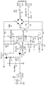
도 1은 스위치 모드 전원 공급 장치에 대한 가능한 일 실시예를 도시한다. 먼저, 80 내지 230 볼트의 전압을 갖는 AC 입력은 퓨즈(F1) 및 저항기(R2)를 통해 다이오드 브리지의 입력 단자 중 하나에 전송된다. 다른 입력선은 저항기(R1)를 통해 다이오드 브리지의 다른 측에 연결된다. 다이오드 브리지의 출력은 음의 전압을 형성하는 일측과 양의 전압을 형성하는 타측에 있다. 커패시터(C1)는 통상적인 DC 전압을 형성하기 위하여 회로의 음의 부분과 양의 부분 사이에 연결된다. 양의 단자로부터 시작하여, 제1 전류 루프(1)는 상대적으로 큰 저항기(R3, R4)에 의해 형성된다. 또한, 제1 전류 루프는 다이오드(D1)와 저항기(R5)를 포함한다. 또한, 제1 전류 류프는 이미터가 음의 전원 단자에 연결된 트랜지스터(Q2)의 콜렉터에 연결된다. 또한, 제2 전류 루프(2)는 양의 단자로부터 시작하여 변압기의 1차측에 연결되고, 1차측은 코일의 반대측에서 트랜지스터(Q1)의 콜렉터에 연결된다. 트랜지스터(Q1)의 이미터는 저항기(R6)를 통해 음의 단자에 연결된다. 트랜지스터(Q1)의 베이스는 저항기(R5)와 트랜지스터(Q2)의 콜렉터에 연결된다. 또한, 트랜지스터(Q2)의 베이스는 트랜지스터(Q1)의 이미터와 저항기(R6)에 연결된다. 변압기의 2차측은 다이오드(D2)를 통해 커패시터(C3)에 연결된다. 또한, 다이오드(D2)는 저항기(R7)를 통해 제너 다이오드(Z1)와 광 커플러(ISO1)의 전송부에 연결된다. 광 트랜지스터인 광커플러의 수신부는 음의 전압에 연결된 이미터를 가지며, 콜렉터는 트랜지스터(Q2)의 콜렉터와, 역시 트랜지스터(Q1)의 베이스에 연결된 저항기(R5) 사이에서 제1 전류 루프에 연결된다. 출력은 도시된 예에서 6V로 감소된 전압으로 전력 조절을 수행할 수 있는 조절 유닛(U1)에 또한 연결된다.
1 shows one possible embodiment for a switch mode power supply. First, an AC input with a voltage of 80 to 230 volts is sent to one of the input terminals of the diode bridge through fuse F1 and resistor R2. The other input line is connected to the other side of the diode bridge via resistor R1. The output of the diode bridge is on one side to form a negative voltage and the other to form a positive voltage. Capacitor C1 is connected between the negative and positive portions of the circuit to form a conventional DC voltage. Starting from the positive terminal, the first
작동시, 다이오드 브리지의 양의 측에 연속하는 DC 전압이 있을 것이다. 따라서, 전류는 제1 전류 루프를 통해 R3, R4, 다이오드(D1) 및 저항기(R5)에 흐르고 있다. 아마도, 트랜지스터(Q2)는 닫힌 상황에 있다. 따라서, 베이스 전류가 트랜지스터(Q1) 대하여 생성된다. 그러나, 광 커플러가 활성화되어 있다면, 전류가 광 커플러로 흐르기 때문에, 트랜지스터(Q1)에 대한 베이스 전류는 생성되지 않는다. 광 커플러가 더 이상 활성화되지 않게 되자마자, 트랜지스터(Q1)에 대한 베이스 전류가 생성되고, 트랜지스터(Q1)는 열기 시작하여, 전류는 제2 전류 루프를 통해 흐른다. 변압기의 1차측은 추가 코일(4, 5)을 포함하며, 코일은 일측에서 음의 단자에 연결되고, 타측은 커패시터(C2)를 통해 제2 전류 루프에 연결된다. 이에 의해, 트랜지스터(Q1)가 제2 전류 루프를 통해 흐르는 전류를 위하여 열기 시작하면, 추가의 개방 전류가 트랜지스터(Q1)에 대하여 생성된다. 이에 의해, 변압기를 통한 전류의 2단계 활성화가 획득될 수 있다. 전류가 변압기의 1차측과 트랜지스터(Q1)를 통해 흐르기 시작하자마자, 저항기(R6)는 트랜지스터(Q2)로의 베이스 전류를 생성하는 증가하는 전압을 가지며, 그 다음 트랜지스터(Q2)는 개방된다. 또한, 트랜지스터(Q2)의 개방은 트랜지스터(Q1)로부터의 베이스 전류를 제거하고, 그 다음 트랜지스터(Q1)는 닫힌다. 이에 의해, 저항기(R6)를 통해 흐르는 전류는 감소하고, 트랜지스터(Q2)에 대한 베이스 전류는 트랜지스터(Q2)가 전도를 정지함에 따라 감소한다. 따라서, 스위칭은 각 단일 발진 후에 정지한다. 다음의 발진은 저출력 전압의 상황에서만 개시한다. 출력 전압이 제너 다이오드(Z1) 및 광 커플러(ISO1)의 발광 다이오드를 통해 충분한 전류를 전송할 수 있는 한, 광 커플러에서의 트랜지스터가 전도하게 한다. 이에 의해, 트랜지스터(Q1)의 베이스 전류는 감소되고, 트랜지스터(Q1)는 광 커플러에서의 전류가 정지되기 전에 전도를 개시할 수 없다.
In operation, there will be a continuous DC voltage on the positive side of the diode bridge. Thus, current is flowing through the first current loop to R3, R4, diode D1 and resistor R5. Perhaps transistor Q2 is in a closed situation. Thus, a base current is generated for transistor Q1. However, if the optocoupler is active, the base current for transistor Q1 is not generated because current flows to the optocoupler. As soon as the optocoupler is no longer active, a base current for transistor Q1 is generated, and transistor Q1 begins to open, so that current flows through the second current loop. The primary side of the transformer comprises
이에 의해, 고효율의 스위치 모드 전원 공급 장치가 획득된다.
Thereby, a high efficiency switch mode power supply is obtained.
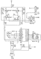
도 2는 도 1에 도시된 바와 같은 스위치 모드 전원 공급 장치에 연결될 수 있는 릴레이 회로를 도시한다. 릴레이 회로는 전자 스위칭 브리지를 포함하고, 브리지의 4개의 트랜지스터는 다리를 형성하며, 양 브리지의 중점은 쌍안정(bi-stable) 릴레이(LS1)에서 릴레이 코일의 각 측에 연결된다. 브리지에서의 제1 다리는 2개의 트랜지스터(Q11, Q9)로 이루어진다. 트랜지스터(Q11)의 베이스는 저항기(R10)를 통해 양의 전원에 연결되고, 저항기(R11)를 통해 릴레이 코일의 일 부분에 연결된다. 브리지의 다른 다리는 트랜지스터(Q12)와 트랜지스터(Q10)로 이루어진다. 또한, 트랜지스터(Q12)의 베이스는 저항기(R11)을 통해 양의 전원에 연결되고 저항기(R13)을 통해 릴레이 코일의 반대측에 연결된다. 브릿지의 트랜지스터(Q9, Q10)는 모두 접지에 연결된 이미터를 가진다. 또한, 브리지의 중점은 브리지의 양측으로부터의 콜렉터 연결부이다. 이러한 중점은 릴레이 코일의 각 측에 연결된다. 릴레이 코일은 저항기(R11, R13)를 통해 트랜지스터(Q11, Q12)의 베이스에 또한 연결된다. 트랜지스터(Q9, Q10) 모두의 베이스는 저항기(R14, R15)에 의해 프로세서(IC1)에 연결된다. 이 프로세서(IC1)는 메모리(IC2)에 더 연결된다. 또한, IC1은 클록 주파수를 내부에서 생성하기 위하여 수정(Y1)에 연결된다. 프로세서(IC1)는 임의의 종류의 입력 수단에 대한 연결을 위한 케이블 또는 다른 통신 수단일 수 있는 입력 장치에 연결된 입력 라인을 가진다.
FIG. 2 shows a relay circuit that may be connected to a switch mode power supply as shown in FIG. 1. The relay circuit includes an electronic switching bridge, the four transistors of the bridge form a bridge, and the midpoint of both bridges is connected to each side of the relay coil in a bi-stable relay LS1. The first leg in the bridge consists of two transistors Q11 and Q9. The base of transistor Q11 is connected to a positive power supply via resistor R10 and to a portion of the relay coil through resistor R11. The other leg of the bridge consists of transistor Q12 and transistor Q10. In addition, the base of transistor Q12 is connected to the positive power supply via resistor R11 and to the opposite side of the relay coil through resistor R13. The transistors Q9 and Q10 of the bridge both have emitters connected to ground. Also, the midpoint of the bridge is the collector connection from both sides of the bridge. This midpoint is connected to each side of the relay coil. The relay coil is also connected to the base of transistors Q11 and Q12 via resistors R11 and R13. The base of both transistors Q9 and Q10 is connected to processor IC1 by resistors R14 and R15. This processor IC1 is further connected to the memory IC2. IC1 is also coupled to crystal Y1 to internally generate the clock frequency. The processor IC1 has an input line connected to the input device, which may be a cable or other communication means for connection to any kind of input means.
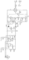
도 3은 도 1 및 도 2의 조합을 도시한다.3 shows a combination of FIGS. 1 and 2.
Claims (8)
상기 피드백 회로는 광 커플러를 포함하고, 상기 광 커플러의 입력 LED는 전류 및 전압 제한 회로를 통해 상기 출력 전압에 연결되고, 상기 저전력 스위치 모드 전원 공급 장치는 전압 분배기의 형태의 제1 전류 루프를 포함하고, 상기 전압 분배기는 적어도 하나의 큰 저항기(R3, R4)를 통해 DC 전원에 연결되고, 상기 큰 저항기(R3, R4)는 제1 트랜지스터(Q1)의 베이스에 연결되고, 상기 전압 분배기는 제2 트랜지스터(Q2)의 콜렉터에 연결되고, 상기 제2 트랜지스터(Q2)의 이미터는 접지에 연결되고, 상기 저전력 스위치 모드 전원 공급 장치는 제1 단이 상기 DC 전원에 연결되고 제2 단이 상기 제1 트랜지스터(Q1)의 콜렉터/이미터에 연결된 상기 변압기의 1차 코일의 형태의 제2 전류 루프를 포함하고, 상기 제2 전류 루프는 저항기(R6)를 더 포함하고, 상기 저항기(R6)는 접지에 연결되고, 상기 제1 트랜지스터(Q1)의 베이스는 상기 광 커플러의 출력 트랜지스터에 또한 연결되는 것을 특징으로 하는,
저전력 스위치 모드 전원 공급 장치.
A primary oscillation circuit and a feedback circuit, said primary oscillation circuit being connected to a DC power supply, said primary oscillating circuit being connected to a first primary coil of a transformer, said transformer being at least a first secondary coil; Wherein the secondary coil is connected to an output circuit through a rectifier, the output circuit including at least a first capacitor forming a typical DC output voltage, the feedback circuit for controlling the primary switching circuit. In a low power switch mode power supply using an actual output voltage,
The feedback circuit comprises an optocoupler, the input LED of the optocoupler being connected to the output voltage via a current and voltage limiting circuit, the low power switch mode power supply comprising a first current loop in the form of a voltage divider. The voltage divider is connected to the DC power supply through at least one large resistor (R3, R4), the large resistor (R3, R4) is connected to the base of the first transistor (Q1), and the voltage divider A second transistor Q2, a emitter of the second transistor Q2, a ground, a low power switch mode power supply having a first end connected to the DC power supply and a second end A second current loop in the form of a primary coil of the transformer connected to the collector / emitter of the first transistor Q1, the second current loop further comprising a resistor R6, the resistor R6 being Is connected on whether the base of the first transistor (Q1) is characterized in that also connected to the output transistor of the optocoupler,
Low power switch mode power supply.
상기 변압기는 제2 1차 코일을 포함하며, 상기 코일은 일단에 의해 접지에 연결되고, 상기 제2 1차 코일의 제2 단은 상기 제1 전류 루프의 상기 전압 분배기에 연결되는 것을 특징으로 하는,
저전력 스위치 모드 전원 공급 장치.
The method of claim 1,
The transformer comprises a second primary coil, the coil being connected to ground by one end, and the second end of the second primary coil being connected to the voltage divider of the first current loop. ,
Low power switch mode power supply.
스탠바이 상황에서의 상기 발진기의 단일 스위칭 시컨스는 초당 한 번의 속도로 수행되는 것을 특징으로 하는,
저전력 스위치 모드 전원 공급 장치.
The method according to claim 1 or 2,
Characterized in that the single switching sequence of the oscillator in a standby situation is performed at a rate of once per second,
Low power switch mode power supply.
저전력 릴레이 유닛은 상기 저전력 스위치 모드 전원 공급 장치로부터 작동 전력을 공급받고, 상기 릴레이 유닛은 쌍안정(bi-stable) 릴레이를 포함하고, 상기 쌍안정 릴레이는 제어 회로에 연결된 코일을 가지고, 상기 제어 회로는 제1 및 제2 전류 루프를 포함하고, 상기 제1 및 제2 전류 루프 각각은 전자 브리지를 형성하는 2개의 전자 스위치를 포함하고, 상기 릴레이 유닛의 코일은 상기 브리지의 상기 스위치 사이에 연결되고, 적어도 하나의 상기 전자 스위치는 프로세서에 연결되고, 상기 프로세스는 상기 전자 스위치를 위한 활성화 펄스를 생성하고, 상기 프로세서는 입력 장치에 또한 연결되는 것을 특징으로 하는,
저전력 스위치 모드 전원 공급 장치.
4. The method according to any one of claims 1 to 3,
The low power relay unit receives operating power from the low power switch mode power supply, the relay unit comprises a bi-stable relay, the bistable relay having a coil connected to a control circuit, the control circuit Includes first and second current loops, each of the first and second current loops comprising two electronic switches forming an electronic bridge, the coil of the relay unit being connected between the switches of the bridge and At least one said electronic switch is connected to a processor, said process generates an activation pulse for said electronic switch, said processor is also connected to an input device,
Low power switch mode power supply.
상기 저전력 스위치 모드 전원 공급 장치는 릴레이 장치에 전력을 공급하는데 사용되고, 상기 릴레이 유닛은 쌍안정 릴레이의 위치를 제어하고, 상기 릴레이 유닛은 입력 신호에 기초하여 상기 쌍안정 릴레이의 위치를 변경하는 것을 특징으로 하는,
저전력 스위치 모드 전원 공급 장치.
The method of claim 4, wherein
The low power switch mode power supply is used to supply power to a relay device, the relay unit controls the position of the bistable relay, and the relay unit changes the position of the bistable relay based on an input signal. Made,
Low power switch mode power supply.
상기 릴레이 유닛은 통신 장치로부터 입력 신호를 공급받는 것을 특징으로 하는,
저전력 스위치 모드 전원 공급 장치.
The method of claim 5,
The relay unit is characterized in that the input signal is supplied from the communication device,
Low power switch mode power supply.
상기 전원 공급 장치 및 상기 릴레이 장치는 전력 소비 기기의 전원 공급 장치의 일부인 것을 특징으로 하는,
저전력 스위치 모드 전원 공급 장치.
7. The method according to any one of claims 4 to 6,
The power supply device and the relay device are part of a power supply device of a power consuming device,
Low power switch mode power supply.
상기 발진기는 제1 및 제2 전류 루프를 포함하고, 상기 제1 전류 루프는 상기 제2 전류 루프에 대한 활성화 전류를 생성하고, 변압기의 1차 코일은 상기 제2 전류 루프의 일부이고, 상기 제2 전류 루프는 전류/전압 측정 시스템을 포함하여 상기 제2 전류 루프에서 증가하는 전류를 생성하고 상기 제2 전류 루프에서의 전류 흐름을 닫는,
저전력 스위치 모드 전원 공급 장치 작동 방법.Conventional DC input power is converted into AC power by an oscillator, AC power is converted into AC voltage and AC current, output power is converted into DC power, and the output DC voltage is used as a feedback signal to control the oscillator. A method of operating a low power switch mode power supply,
The oscillator comprises first and second current loops, the first current loop generating an activation current for the second current loop, the primary coil of the transformer being part of the second current loop, The second current loop includes a current / voltage measurement system to generate an increasing current in the second current loop and to close the current flow in the second current loop,
How a low power switch mode power supply works.
Applications Claiming Priority (2)
| Application Number | Priority Date | Filing Date | Title |
|---|---|---|---|
| DKPA200900930 | 2009-08-14 | ||
| DKPA200900930A DK177105B1 (en) | 2009-08-14 | 2009-08-14 | Low power switch mode power supply and use of the power supply |
Publications (1)
| Publication Number | Publication Date |
|---|---|
| KR20120050482A true KR20120050482A (en) | 2012-05-18 |
Family
ID=43585980
Family Applications (1)
| Application Number | Title | Priority Date | Filing Date |
|---|---|---|---|
| KR1020127006530A KR20120050482A (en) | 2009-08-14 | 2010-08-10 | Low power switch mode power supply |
Country Status (8)
| Country | Link |
|---|---|
| US (1) | US8885361B2 (en) |
| EP (1) | EP2465191A4 (en) |
| JP (1) | JP2013502195A (en) |
| KR (1) | KR20120050482A (en) |
| CN (1) | CN102498654A (en) |
| AU (1) | AU2010281960A1 (en) |
| DK (1) | DK177105B1 (en) |
| WO (1) | WO2011018089A1 (en) |
Cited By (1)
| Publication number | Priority date | Publication date | Assignee | Title |
|---|---|---|---|---|
| KR101594330B1 (en) | 2014-10-31 | 2016-02-16 | (주)자람테크놀로지 | The method and apparatus for low power conversion based on reduction of switching energy |
Families Citing this family (8)
| Publication number | Priority date | Publication date | Assignee | Title |
|---|---|---|---|---|
| CN103199710A (en) * | 2013-04-01 | 2013-07-10 | 上海师范大学 | Low-power consumption standby switching power source |
| KR102300316B1 (en) | 2014-03-06 | 2021-09-10 | 삼성디스플레이 주식회사 | Stand-by power controlling device, liquid crystal display device including the same, and method of controlling stand-by power |
| CN103872885B (en) * | 2014-03-18 | 2016-04-06 | 深圳市华星光电技术有限公司 | A kind of standby power consumption control circuit and method |
| DE102014217124A1 (en) | 2014-08-28 | 2016-03-03 | BSH Hausgeräte GmbH | Pulsed energy converter for supplying energy to an electronic control unit of a household appliance |
| WO2016188880A1 (en) * | 2015-05-22 | 2016-12-01 | Philips Lighting Holding B.V. | Led driver and an led driving method |
| US10014774B2 (en) * | 2016-10-18 | 2018-07-03 | Texas Instruments Incorporated | Power supply with low to high power transition mode |
| CN106952781B (en) * | 2017-04-18 | 2019-03-12 | 福州大学 | A kind of intelligent contactor control module using double feedback factor control strategies |
| CN113625151A (en) * | 2021-07-08 | 2021-11-09 | 南方电网科学研究院有限责任公司 | Test system for special module of electric power |
Family Cites Families (16)
| Publication number | Priority date | Publication date | Assignee | Title |
|---|---|---|---|---|
| JPS6047834B2 (en) * | 1980-12-01 | 1985-10-23 | オムロン株式会社 | switching regulator |
| DE3566759D1 (en) * | 1984-08-07 | 1989-01-12 | Siemens Ag | Power supply with free oscillating forward converter and electrically insolated control loop |
| US4737898A (en) * | 1987-02-13 | 1988-04-12 | Northern Telecom Limited | Single-ended self-oscillating, DC-DC converter with regulation and inhibit control |
| JPS63134434U (en) * | 1987-02-25 | 1988-09-02 | ||
| US4903182A (en) * | 1989-03-20 | 1990-02-20 | American Telephone And Telegraph Company, At&T Bell Laboratories | Self-oscillating converter with light load stabilizer |
| DE4121961A1 (en) * | 1991-06-28 | 1993-01-07 | Siemens Ag | CIRCUIT FOR THE ENERGY SUPPLY OF FIELD DEVICES |
| DE4438388A1 (en) * | 1994-10-27 | 1996-05-02 | Ant Nachrichtentech | Self-oscillating transformer-type DC=DC converter |
| JP2000113788A (en) * | 1998-10-07 | 2000-04-21 | Omron Corp | Drive circuit for self-holding electromagnetic relay, and power supply control circuit |
| JP2002244743A (en) * | 2001-02-19 | 2002-08-30 | Matsushita Electric Ind Co Ltd | Stand-by power supply circuit |
| FI118026B (en) * | 2001-08-07 | 2007-05-31 | Salcomp Oy | Use of the rectified voltage on the primary-side switching power source control switch |
| JP2003304686A (en) * | 2002-04-05 | 2003-10-24 | Yutaka Denki Seisakusho:Kk | Switching power circuit |
| US6956761B2 (en) * | 2004-03-10 | 2005-10-18 | Micron Technology, Inc. | Method to manufacture polymer memory with copper ion switching species |
| US20060209574A1 (en) * | 2005-03-17 | 2006-09-21 | Creative Technology, Ltd. | Power supply |
| US7675760B2 (en) * | 2005-03-17 | 2010-03-09 | Creative Technology Ltd. | Power supply |
| EP1798845A1 (en) | 2005-12-16 | 2007-06-20 | Advanced Digital Broadcast S.A. | Multi-output switched-mode power supply |
| EP2153453B1 (en) * | 2007-05-31 | 2012-01-11 | Arçelik Anonim Sirketi | An electric motor |
-
2009
- 2009-08-14 DK DKPA200900930A patent/DK177105B1/en active
-
2010
- 2010-08-10 EP EP10808001.1A patent/EP2465191A4/en not_active Withdrawn
- 2010-08-10 WO PCT/DK2010/050205 patent/WO2011018089A1/en active Application Filing
- 2010-08-10 CN CN2010800359230A patent/CN102498654A/en active Pending
- 2010-08-10 JP JP2012524116A patent/JP2013502195A/en active Pending
- 2010-08-10 KR KR1020127006530A patent/KR20120050482A/en not_active Application Discontinuation
- 2010-08-10 AU AU2010281960A patent/AU2010281960A1/en not_active Abandoned
-
2012
- 2012-02-14 US US13/372,551 patent/US8885361B2/en not_active Expired - Fee Related
Cited By (1)
| Publication number | Priority date | Publication date | Assignee | Title |
|---|---|---|---|---|
| KR101594330B1 (en) | 2014-10-31 | 2016-02-16 | (주)자람테크놀로지 | The method and apparatus for low power conversion based on reduction of switching energy |
Also Published As
| Publication number | Publication date |
|---|---|
| WO2011018089A1 (en) | 2011-02-17 |
| EP2465191A1 (en) | 2012-06-20 |
| DK200900930A (en) | 2011-02-15 |
| US8885361B2 (en) | 2014-11-11 |
| AU2010281960A1 (en) | 2012-03-22 |
| EP2465191A4 (en) | 2013-07-31 |
| US20120212978A1 (en) | 2012-08-23 |
| JP2013502195A (en) | 2013-01-17 |
| CN102498654A (en) | 2012-06-13 |
| DK177105B1 (en) | 2011-09-05 |
Similar Documents
| Publication | Publication Date | Title |
|---|---|---|
| KR20120050482A (en) | Low power switch mode power supply | |
| CN102013807B (en) | Method and apparatus for increasing the power capability of a power supply | |
| KR100667468B1 (en) | Dc-dc converter | |
| CN101572499B (en) | Switching controller with intermittent electricity-saving mode management circuit | |
| CN102739018B (en) | Burst-mode operation of a switching converter | |
| KR20010051532A (en) | Circuit for reducing standby power of electric apparatus | |
| WO2010003785A2 (en) | Power supply unit having a voltage converter | |
| CN203788138U (en) | Starting circuit | |
| JP2000278945A (en) | Switching power supply device | |
| US6924630B1 (en) | Buck-boost power factory correction circuit | |
| JP2001008451A (en) | Pulse width modulation controller | |
| CN115065051A (en) | Signal injection circuit and injection method | |
| RU2586240C2 (en) | Surgical device with improved network module | |
| KR100532518B1 (en) | Method for starting a switching power supply and a switching power supply comprising a starting circuit | |
| CN102594148A (en) | Feedback circuit with remote control for power supply | |
| CN102208303A (en) | Relay driver circuit | |
| EP0749199A1 (en) | Power supply for an appliance having an operating mode and a stand-by mode | |
| JP2010098875A (en) | Power supply apparatus | |
| JP3344479B2 (en) | Chopper type switching power supply | |
| JP4348493B2 (en) | Power circuit | |
| EP2278687A1 (en) | Electrical apparatus having a solar power supply | |
| CN215221823U (en) | Active remote control type pure hardware automatic transfer switch circuit | |
| KR102661090B1 (en) | Hybrid switch control device | |
| JP5920657B2 (en) | AC adapter | |
| JP5169660B2 (en) | Control device and air conditioner |
Legal Events
| Date | Code | Title | Description |
|---|---|---|---|
| WITN | Application deemed withdrawn, e.g. because no request for examination was filed or no examination fee was paid |