KR20120044021A - Flat panel display apparatus and method of manufacturing flat panel display apparatus - Google Patents
Flat panel display apparatus and method of manufacturing flat panel display apparatus Download PDFInfo
- Publication number
- KR20120044021A KR20120044021A KR1020100105376A KR20100105376A KR20120044021A KR 20120044021 A KR20120044021 A KR 20120044021A KR 1020100105376 A KR1020100105376 A KR 1020100105376A KR 20100105376 A KR20100105376 A KR 20100105376A KR 20120044021 A KR20120044021 A KR 20120044021A
- Authority
- KR
- South Korea
- Prior art keywords
- inlet
- group
- inlet group
- sealing member
- spaced apart
- Prior art date
Links
- 238000004519 manufacturing process Methods 0.000 title claims abstract description 19
- 238000007789 sealing Methods 0.000 claims abstract description 188
- 239000000758 substrate Substances 0.000 claims abstract description 105
- 239000000463 material Substances 0.000 claims description 38
- 238000000034 method Methods 0.000 claims description 35
- 239000004973 liquid crystal related substance Substances 0.000 claims description 6
- 238000007373 indentation Methods 0.000 claims description 4
- 239000010410 layer Substances 0.000 description 27
- 238000002844 melting Methods 0.000 description 8
- 230000008018 melting Effects 0.000 description 8
- 229920000642 polymer Polymers 0.000 description 8
- 238000005538 encapsulation Methods 0.000 description 7
- 238000002161 passivation Methods 0.000 description 4
- -1 polyethylene naphthalate Polymers 0.000 description 4
- 239000004697 Polyetherimide Substances 0.000 description 3
- 229910004298 SiO 2 Inorganic materials 0.000 description 3
- 230000002159 abnormal effect Effects 0.000 description 3
- 229910045601 alloy Inorganic materials 0.000 description 3
- 239000000956 alloy Substances 0.000 description 3
- 229910052782 aluminium Inorganic materials 0.000 description 3
- 239000004020 conductor Substances 0.000 description 3
- 230000020169 heat generation Effects 0.000 description 3
- 229910052751 metal Inorganic materials 0.000 description 3
- 239000002184 metal Substances 0.000 description 3
- 229910052750 molybdenum Inorganic materials 0.000 description 3
- 239000011368 organic material Substances 0.000 description 3
- 229920000058 polyacrylate Polymers 0.000 description 3
- 229920001601 polyetherimide Polymers 0.000 description 3
- 239000004065 semiconductor Substances 0.000 description 3
- IJGRMHOSHXDMSA-UHFFFAOYSA-N Atomic nitrogen Chemical compound N#N IJGRMHOSHXDMSA-UHFFFAOYSA-N 0.000 description 2
- 229920008347 Cellulose acetate propionate Polymers 0.000 description 2
- 239000004734 Polyphenylene sulfide Substances 0.000 description 2
- 229910004205 SiNX Inorganic materials 0.000 description 2
- 229910021417 amorphous silicon Inorganic materials 0.000 description 2
- 229910052737 gold Inorganic materials 0.000 description 2
- 238000003780 insertion Methods 0.000 description 2
- 230000037431 insertion Effects 0.000 description 2
- 239000011229 interlayer Substances 0.000 description 2
- 229910052759 nickel Inorganic materials 0.000 description 2
- 229910052763 palladium Inorganic materials 0.000 description 2
- 229920003023 plastic Polymers 0.000 description 2
- 229910052697 platinum Inorganic materials 0.000 description 2
- 229920003207 poly(ethylene-2,6-naphthalate) Polymers 0.000 description 2
- 229910021420 polycrystalline silicon Inorganic materials 0.000 description 2
- 239000011112 polyethylene naphthalate Substances 0.000 description 2
- 229920000139 polyethylene terephthalate Polymers 0.000 description 2
- 239000005020 polyethylene terephthalate Substances 0.000 description 2
- 229920000069 polyphenylene sulfide Polymers 0.000 description 2
- 229920005591 polysilicon Polymers 0.000 description 2
- 229910018072 Al 2 O 3 Inorganic materials 0.000 description 1
- ZOXJGFHDIHLPTG-UHFFFAOYSA-N Boron Chemical compound [B] ZOXJGFHDIHLPTG-UHFFFAOYSA-N 0.000 description 1
- 229920002284 Cellulose triacetate Polymers 0.000 description 1
- IMROMDMJAWUWLK-UHFFFAOYSA-N Ethenol Chemical compound OC=C IMROMDMJAWUWLK-UHFFFAOYSA-N 0.000 description 1
- YCKRFDGAMUMZLT-UHFFFAOYSA-N Fluorine atom Chemical compound [F] YCKRFDGAMUMZLT-UHFFFAOYSA-N 0.000 description 1
- 229910000583 Nd alloy Inorganic materials 0.000 description 1
- 229910052779 Neodymium Inorganic materials 0.000 description 1
- 229920002873 Polyethylenimine Polymers 0.000 description 1
- 239000004642 Polyimide Substances 0.000 description 1
- 229910010413 TiO 2 Inorganic materials 0.000 description 1
- 229910001080 W alloy Inorganic materials 0.000 description 1
- NNLVGZFZQQXQNW-ADJNRHBOSA-N [(2r,3r,4s,5r,6s)-4,5-diacetyloxy-3-[(2s,3r,4s,5r,6r)-3,4,5-triacetyloxy-6-(acetyloxymethyl)oxan-2-yl]oxy-6-[(2r,3r,4s,5r,6s)-4,5,6-triacetyloxy-2-(acetyloxymethyl)oxan-3-yl]oxyoxan-2-yl]methyl acetate Chemical compound O([C@@H]1O[C@@H]([C@H]([C@H](OC(C)=O)[C@H]1OC(C)=O)O[C@H]1[C@@H]([C@@H](OC(C)=O)[C@H](OC(C)=O)[C@@H](COC(C)=O)O1)OC(C)=O)COC(=O)C)[C@@H]1[C@@H](COC(C)=O)O[C@@H](OC(C)=O)[C@H](OC(C)=O)[C@H]1OC(C)=O NNLVGZFZQQXQNW-ADJNRHBOSA-N 0.000 description 1
- 239000000853 adhesive Substances 0.000 description 1
- 230000001070 adhesive effect Effects 0.000 description 1
- 150000001408 amides Chemical class 0.000 description 1
- 150000008378 aryl ethers Chemical class 0.000 description 1
- 229910052796 boron Inorganic materials 0.000 description 1
- 229920002678 cellulose Polymers 0.000 description 1
- 239000001913 cellulose Substances 0.000 description 1
- HKQOBOMRSSHSTC-UHFFFAOYSA-N cellulose acetate Chemical compound OC1C(O)C(O)C(CO)OC1OC1C(CO)OC(O)C(O)C1O.CC(=O)OCC1OC(OC(C)=O)C(OC(C)=O)C(OC(C)=O)C1OC1C(OC(C)=O)C(OC(C)=O)C(OC(C)=O)C(COC(C)=O)O1.CCC(=O)OCC1OC(OC(=O)CC)C(OC(=O)CC)C(OC(=O)CC)C1OC1C(OC(=O)CC)C(OC(=O)CC)C(OC(=O)CC)C(COC(=O)CC)O1 HKQOBOMRSSHSTC-UHFFFAOYSA-N 0.000 description 1
- 239000002131 composite material Substances 0.000 description 1
- 229910052802 copper Inorganic materials 0.000 description 1
- 230000008878 coupling Effects 0.000 description 1
- 238000010168 coupling process Methods 0.000 description 1
- 238000005859 coupling reaction Methods 0.000 description 1
- 229910052731 fluorine Inorganic materials 0.000 description 1
- 239000011737 fluorine Substances 0.000 description 1
- 239000007789 gas Substances 0.000 description 1
- 239000011521 glass Substances 0.000 description 1
- 229910021478 group 5 element Inorganic materials 0.000 description 1
- 150000003949 imides Chemical class 0.000 description 1
- 239000012535 impurity Substances 0.000 description 1
- 229910010272 inorganic material Inorganic materials 0.000 description 1
- 239000011147 inorganic material Substances 0.000 description 1
- 239000012212 insulator Substances 0.000 description 1
- 229910052741 iridium Inorganic materials 0.000 description 1
- 150000002739 metals Chemical class 0.000 description 1
- 239000000203 mixture Substances 0.000 description 1
- 238000012986 modification Methods 0.000 description 1
- 230000004048 modification Effects 0.000 description 1
- 229910052757 nitrogen Inorganic materials 0.000 description 1
- 229910052762 osmium Inorganic materials 0.000 description 1
- 230000000149 penetrating effect Effects 0.000 description 1
- ISWSIDIOOBJBQZ-UHFFFAOYSA-N phenol group Chemical group C1(=CC=CC=C1)O ISWSIDIOOBJBQZ-UHFFFAOYSA-N 0.000 description 1
- 239000004033 plastic Substances 0.000 description 1
- 229920003229 poly(methyl methacrylate) Polymers 0.000 description 1
- 239000004417 polycarbonate Substances 0.000 description 1
- 229920000515 polycarbonate Polymers 0.000 description 1
- 229920001721 polyimide Polymers 0.000 description 1
- 239000004926 polymethyl methacrylate Substances 0.000 description 1
- 229910052703 rhodium Inorganic materials 0.000 description 1
- 229910052707 ruthenium Inorganic materials 0.000 description 1
- 229910052814 silicon oxide Inorganic materials 0.000 description 1
- 229910052709 silver Inorganic materials 0.000 description 1
- ILJSQTXMGCGYMG-UHFFFAOYSA-N triacetic acid Chemical compound CC(=O)CC(=O)CC(O)=O ILJSQTXMGCGYMG-UHFFFAOYSA-N 0.000 description 1
Images


Classifications
-
- H—ELECTRICITY
- H10—SEMICONDUCTOR DEVICES; ELECTRIC SOLID-STATE DEVICES NOT OTHERWISE PROVIDED FOR
- H10K—ORGANIC ELECTRIC SOLID-STATE DEVICES
- H10K59/00—Integrated devices, or assemblies of multiple devices, comprising at least one organic light-emitting element covered by group H10K50/00
- H10K59/10—OLED displays
- H10K59/12—Active-matrix OLED [AMOLED] displays
- H10K59/131—Interconnections, e.g. wiring lines or terminals
-
- G—PHYSICS
- G02—OPTICS
- G02F—OPTICAL DEVICES OR ARRANGEMENTS FOR THE CONTROL OF LIGHT BY MODIFICATION OF THE OPTICAL PROPERTIES OF THE MEDIA OF THE ELEMENTS INVOLVED THEREIN; NON-LINEAR OPTICS; FREQUENCY-CHANGING OF LIGHT; OPTICAL LOGIC ELEMENTS; OPTICAL ANALOGUE/DIGITAL CONVERTERS
- G02F1/00—Devices or arrangements for the control of the intensity, colour, phase, polarisation or direction of light arriving from an independent light source, e.g. switching, gating or modulating; Non-linear optics
- G02F1/01—Devices or arrangements for the control of the intensity, colour, phase, polarisation or direction of light arriving from an independent light source, e.g. switching, gating or modulating; Non-linear optics for the control of the intensity, phase, polarisation or colour
- G02F1/13—Devices or arrangements for the control of the intensity, colour, phase, polarisation or direction of light arriving from an independent light source, e.g. switching, gating or modulating; Non-linear optics for the control of the intensity, phase, polarisation or colour based on liquid crystals, e.g. single liquid crystal display cells
- G02F1/133—Constructional arrangements; Operation of liquid crystal cells; Circuit arrangements
- G02F1/1333—Constructional arrangements; Manufacturing methods
- G02F1/1339—Gaskets; Spacers; Sealing of cells
-
- H—ELECTRICITY
- H10—SEMICONDUCTOR DEVICES; ELECTRIC SOLID-STATE DEVICES NOT OTHERWISE PROVIDED FOR
- H10K—ORGANIC ELECTRIC SOLID-STATE DEVICES
- H10K50/00—Organic light-emitting devices
- H10K50/80—Constructional details
- H10K50/84—Passivation; Containers; Encapsulations
- H10K50/842—Containers
- H10K50/8426—Peripheral sealing arrangements, e.g. adhesives, sealants
-
- H—ELECTRICITY
- H10—SEMICONDUCTOR DEVICES; ELECTRIC SOLID-STATE DEVICES NOT OTHERWISE PROVIDED FOR
- H10K—ORGANIC ELECTRIC SOLID-STATE DEVICES
- H10K59/00—Integrated devices, or assemblies of multiple devices, comprising at least one organic light-emitting element covered by group H10K50/00
- H10K59/80—Constructional details
- H10K59/87—Passivation; Containers; Encapsulations
- H10K59/871—Self-supporting sealing arrangements
- H10K59/8722—Peripheral sealing arrangements, e.g. adhesives, sealants
-
- G—PHYSICS
- G02—OPTICS
- G02F—OPTICAL DEVICES OR ARRANGEMENTS FOR THE CONTROL OF LIGHT BY MODIFICATION OF THE OPTICAL PROPERTIES OF THE MEDIA OF THE ELEMENTS INVOLVED THEREIN; NON-LINEAR OPTICS; FREQUENCY-CHANGING OF LIGHT; OPTICAL LOGIC ELEMENTS; OPTICAL ANALOGUE/DIGITAL CONVERTERS
- G02F2201/00—Constructional arrangements not provided for in groups G02F1/00 - G02F7/00
- G02F2201/12—Constructional arrangements not provided for in groups G02F1/00 - G02F7/00 electrode
-
- G—PHYSICS
- G02—OPTICS
- G02F—OPTICAL DEVICES OR ARRANGEMENTS FOR THE CONTROL OF LIGHT BY MODIFICATION OF THE OPTICAL PROPERTIES OF THE MEDIA OF THE ELEMENTS INVOLVED THEREIN; NON-LINEAR OPTICS; FREQUENCY-CHANGING OF LIGHT; OPTICAL LOGIC ELEMENTS; OPTICAL ANALOGUE/DIGITAL CONVERTERS
- G02F2202/00—Materials and properties
- G02F2202/02—Materials and properties organic material
- G02F2202/022—Materials and properties organic material polymeric
- G02F2202/023—Materials and properties organic material polymeric curable
- G02F2202/025—Materials and properties organic material polymeric curable thermocurable
Landscapes
- Physics & Mathematics (AREA)
- Nonlinear Science (AREA)
- Optics & Photonics (AREA)
- Mathematical Physics (AREA)
- Chemical & Material Sciences (AREA)
- Crystallography & Structural Chemistry (AREA)
- General Physics & Mathematics (AREA)
- Engineering & Computer Science (AREA)
- Microelectronics & Electronic Packaging (AREA)
- Electroluminescent Light Sources (AREA)
- Devices For Indicating Variable Information By Combining Individual Elements (AREA)
Abstract
Description
본 발명은 평판 표시 장치 및 평판 표시 장치 제조 방법에 관한 것으로 더 상세하게는 봉지 특성을 향상하는 평판 표시 장치 및 평판 표시 장치 제조 방법에 관한 것이다.BACKGROUND OF THE
근래에 표시 장치는 휴대가 가능한 박형의 평판 표시 장치로 대체되는 추세이다. 특히 유기 발광 표시 장치 및 액정 표시 장치와 같은 평판 표시 장치는 화질 특성이 우수하여 각광받고 있다.In recent years, display devices have been replaced by portable flat panel display devices. In particular, flat panel displays such as an organic light emitting display and a liquid crystal display have been spotlighted for their excellent image quality characteristics.
평판 표시 장치는 기판에 표시부가 배치되고, 표시부를 보호하도록 표시부 상부에 밀봉 기판이 배치된다. 또한 기판과 밀봉 기판 사이에는 씰링 부재가 배치된다.In the flat panel display, a display unit is disposed on a substrate, and a sealing substrate is disposed on the display unit to protect the display unit. In addition, a sealing member is disposed between the substrate and the sealing substrate.
평판 표시 장치는 외부의 수분, 기체 및 기타 이물로부터 표시부를 보호하기 위하여 봉지 공정을 하는데 봉지 특성에 따라 평판 표시 장치의 품질이 크게 영향을 받는다.The flat panel display performs an encapsulation process to protect the display unit from external moisture, gas, and other foreign matter. The quality of the flat panel display is greatly affected by the encapsulation characteristics.
봉지 특성은 밀봉 기판 및 씰링 부재에 의하여 좌우되고, 특히 씰링 부재의 균일한 특성이 중요하다.The sealing property depends on the sealing substrate and the sealing member, and in particular, the uniform property of the sealing member is important.
그러나 씰링 부재를 형성하는 공정이 용이하지 않아 봉지 특성을 향상하는데 한계가 있다.However, the process of forming the sealing member is not easy, there is a limit to improve the sealing characteristics.
본 발명은 봉지 특성을 용이하게 향상하는 평판 표시 장치 및 평판 표시 장치 제조 방법을 제공할 수 있다.The present invention can provide a flat panel display device and a flat panel display device manufacturing method which can easily improve sealing characteristics.
본 발명은 기판, 상기 기판 상에 배치되는 표시부, 상기 표시부와 대향하도록 배치된 밀봉 기판, 상기 기판과 상기 밀봉 기판 사이에 상기 표시부를 둘러싸도록 배치되는 씰링 부재, 상기 기판과 상기 밀봉 기판 사이에 상기 씰링 부재와 중첩되는 영역을 구비하도록 배치되는 배선부 및 외부의 전원을 통하여 전압을 인가받을 수 있도록 형성되고 상기 배선부와 연결되는 세 개 이상의 인입부 그룹을 포함하고, 상기 각 인입부 그룹은 복수의 부(副)인입부를 구비하는 평판 표시 장치 를 개시한다.The present invention provides a substrate, a display unit disposed on the substrate, a sealing substrate disposed to face the display unit, a sealing member disposed to enclose the display unit between the substrate and the sealing substrate, and between the substrate and the sealing substrate. A wiring part disposed to have an area overlapping the sealing member, and three or more inlet part groups formed to receive a voltage through an external power source and connected to the wire part, wherein each inlet part group includes a plurality of inlet parts. Disclosed is a flat panel display having a negative lead portion.
본 발명에 있어서 상기 각 인입부 그룹에 구비된 상기 복수의 부인입부들은 서로 이격될 수 있다.In the present invention, the plurality of denier inlets provided in the respective inlet groups may be spaced apart from each other.
본 발명에 있어서 상기 각 인입부 그룹은 서로 이격된 두개의 부인입부를 구비할 수 있다.In the present invention, each of the inlet groups may include two non-inlet portions spaced apart from each other.
본 발명에 있어서 상기 부인입부의 폭은 상기 배선부의 폭보다 크도록 형성될 수 있다.In the present invention, the width of the non-entrance portion may be formed to be larger than the width of the wiring portion.
본 발명에 있어서 상기 인입부 그룹은 서로 이격되도록 순차적으로 배치되는 제1 인입부 그룹, 제2 인입부 그룹 및 제3 인입부 그룹을 포함하고, 상기 제1 인입부 그룹, 제2 인입부 그룹 및 제3 인입부 그룹은 각각 서로 이격되도록 배치된 두 개의 부인입부들을 구비할 수 있다.In the present invention, the inlet group includes a first inlet group, a second inlet group, and a third inlet group, which are sequentially arranged to be spaced apart from each other, wherein the first inlet group, the second inlet group, and The third entry group may have two denier entries that are arranged to be spaced apart from each other.
본 발명에 있어서 상기 인입부 그룹은 서로 이격되도록 순차적으로 배치되는 제1 인입부 그룹, 제2 인입부 그룹, 제3 인입부 그룹 및 제4 인입부 그룹을 포함하고, 상기 제1 인입부 그룹, 제2 인입부 그룹, 제3 인입부 그룹 및 제4 인입부 그룹은 각각 서로 이격되도록 배치된 두 개의 부인입부들을 구비할 수 있다.In the present invention, the inlet group includes a first inlet group, a second inlet group, a third inlet group, and a fourth inlet group, which are sequentially arranged to be spaced apart from each other, wherein the first inlet group, The second inlet group, the third inlet group, and the fourth inlet group may each have two non-indentations arranged to be spaced apart from each other.
본 발명에 있어서 상기 인입부 그룹은 서로 이격되도록 순차적으로 배치되는 제1 인입부 그룹, 제2 인입부 그룹, 제3 인입부 그룹, 제4 인입부 그룹, 제5 인입부 그룹 및 제6 인입부 그룹을 포함하고, 상기 제1 인입부 그룹, 제2 인입부 그룹, 제3 인입부 그룹, 제4 인입부 그룹, 제5 인입부 그룹 및 제6 인입부 그룹은 각각 서로 이격되도록 배치된 두 개의 부인입부들을 구비할 수 있다.In the present invention, the inlet group may be sequentially arranged to be spaced apart from each other, the first inlet group, the second inlet group, the third inlet group, the fourth inlet group, the fifth inlet group, and the sixth inlet unit. A first inlet group, a second inlet group, a third inlet group, a fourth inlet group, a fifth inlet group, and a sixth inlet group, each including two groups; The denier mouths may be provided.
본 발명에 있어서 상기 배선부는 복수의 배선 부재를 구비할 수 있다.In the present invention, the wiring portion may include a plurality of wiring members.
본 발명에 있어서 상기 배선 부재는 상기 씰링 부재와 중첩되는 영역 중 적어도 일 영역에서 서로 이격되도록 형성될 수 있다.In the present invention, the wiring member may be formed to be spaced apart from each other in at least one region of the region overlapping the sealing member.
본 발명에 있어서 상기 배선 부재는 상기 기판상에 형성되고, 상기 씰링 부재는 상기 배선 부재의 상부 및 상기 복수의 배선 부재 중 인접한 배선 부재들간의 이격된 공간에 배치될 수 있다.In the present invention, the wiring member may be formed on the substrate, and the sealing member may be disposed in a space spaced between an upper portion of the wiring member and adjacent wiring members among the plurality of wiring members.
본 발명에 있어서 상기 씰링 부재는 프릿을 함유할 수 있다.In the present invention, the sealing member may contain a frit.
본 발명에 있어서 상기 표시부는 유기 발광 소자 또는 액정 표시 소자를 구비할 수 있다. In the present invention, the display unit may include an organic light emitting diode or a liquid crystal display.
본 발명의 다른 측면에 따르면 표시부가 배치된 기판을 준비하는 단계, 상기 표시부와 대향하도록 밀봉 기판을 배치하는 단계, 상기 기판과 상기 밀봉 기판 사이에 상기 표시부를 둘러싸는 씰링 부재를 형성하는 단계, 상기 기판과 상기 밀봉 기판 사이에 상기 씰링 부재와 중첩되는 영역을 구비하도록 배선부를 형성하는 단계 및 외부의 전원과 전기적으로 연결될 수 있도록 배치되는 세 개 이상의 인입부 그룹을 형성하는 단계를 포함하고, 상기 각 인입부 그룹은 상기 배선부와 연결되는 복수의 부인입부를 구비하고, 상기 씰링 부재를 형성하는 단계는 상기 씰링 부재를 형성하기 위한 재료를 상기 기판과 상기 밀봉 기판 사이에 배치하고 상기 인입부 그룹 중 인접한 두 개의 인입부 그룹을 순차적으로 선택하여 상기 선택된 두 개의 인입부 그룹에 상기 외부의 전원을 연결하여 전압을 순차적으로 인가하고, 상기 인입부 그룹을 통하여 인가된 전압을 통하여 상기 배선부에서 발생하는 열을 이용하여 상기 씰링 부재를 형성하기 위한 재료를 용융 후 경화하는 단계를 포함하는 평판 표시 장치 제조 방법을 개시한다.According to another aspect of the invention, preparing a substrate on which a display unit is disposed, arranging a sealing substrate to face the display unit, forming a sealing member surrounding the display unit between the substrate and the sealing substrate, Forming a wiring portion between the substrate and the sealing substrate so as to have an area overlapping the sealing member, and forming at least three groups of lead portions arranged to be electrically connected to an external power source; The lead group includes a plurality of non-entrance portions connected to the wiring portion, and the forming of the sealing member includes disposing a material for forming the sealing member between the substrate and the sealing substrate, and among the lead group. The two adjacent entry groups are sequentially selected to be displayed on the two selected entry groups. Applying a voltage sequentially by connecting an external power source, and melting and curing the material for forming the sealing member by using heat generated in the wiring unit through the voltage applied through the lead-in group. A flat panel display manufacturing method is described.
본 발명에 있어서 상기 씰링 부재를 형성하는 단계는 상기 인입부 그룹 중 인접한 두 개의 인입부 그룹을 순차적으로 선택하고, 상기 선택된 두 개의 인입부 그룹은 일 인입부 그룹 및 다른 일 인입부 그룹을 구비하고, 상기 일 인입부 그룹의 부인입부들 중 상기 다른 일 인입부로부터 가장 가까운 부인입부를 제외한 부인입부들 중 하나의 부인입부 및 상기 다른 일 인입부 그룹의 부인입부들 중 상기 일 인입부로부터 가장 가까운 부인입부를 제외한 부인입부들 중 하나의 부인입부를 상기 외부의 전원에 연결하고 전압을 인가하는 단계를 구비할 수 있다.In the present invention, the forming of the sealing member may include sequentially selecting two adjacent inlet groups among the inlet groups, wherein the selected two inlet groups include one inlet group and the other inlet group. A denial of one of the deniers except the denier closest to the other one of the deniers of the one-entry group and the closest one of the deniers of the other one-entry group; One of the denial entrances other than the denial entrance may be connected to the external power source and may be configured to apply a voltage.
본 발명에 있어서 상기 인입부 그룹은 서로 이격되도록 순차적으로 배치되는 제1 인입부 그룹, 제2 인입부 그룹 및 제3 인입부 그룹을 포함하고, 상기 제1 인입부 그룹은 상기 제3 인입부 그룹에 가깝게 배치되는 제1 부인입부A 및 상기 제1 부인입부A와 이격되고 상기 제2 인입부 그룹에 가깝게 배치되는 제1 부인입부B를 구비하고, 상기 제2 인입부 그룹은 상기 제1 인입부 그룹에 가깝게 배치되는 제2 부인입부A 및 상기 제2 부인입부A와 이격되고 상기 제3 인입부 그룹에 가깝게 배치되는 제2 부인입부B를 구비하고, 상기 제3 인입부 그룹은 상기 제2 인입부 그룹에 가깝게 배치되는 제3 부인입부A 및 상기 제3 부인입부A와 이격되고 상기 제1 인입부 그룹에 가깝게 배치되는 제3 부인입부B를 구비하고, 상기 씰링 부재를 형성하는 단계는 상기 제1 부인입부A 및 상기 제2 부인입부B에 상기 외부의 전원을 연결하여 전압을 인가하고 나서, 상기 제2 부인입부A 및 상기 제3 부인입부B에 상기 외부의 전원을 연결하여 전압을 인가하고 나서, 상기 제3 부인입부A 및 상기 제1 부인입부B에 상기 외부의 전원을 연결하여 전압을 인가하는 단계를 구비할 수 있다.In the present invention, the inlet group includes a first inlet group, a second inlet group, and a third inlet group, which are sequentially arranged to be spaced apart from each other, wherein the first inlet group is the third inlet group A first female entry A disposed close to and a first female entry B spaced apart from the first female entry portion A and disposed close to the second entry portion group, wherein the second entry group is the first entry portion; A second non-entrance A disposed close to the group and a second non-entrance B spaced apart from the second non-adopted entry A and disposed close to the third entry group, wherein the third entry group is the second entry And a third non-entrance portion A disposed close to the subgroup and a third non-admission portion B spaced from the third non-entrance portion A and disposed close to the first entry portion group, wherein the forming of the sealing member comprises: 1 Disclaimer A and Award Connecting the external power to the second non-admission part B to apply a voltage, and applying the voltage by connecting the external power source to the second non-admission part A and the third non-admission part B, and then applying the voltage. And applying a voltage by connecting the external power source to the negative entry A and the first negative entry B.
본 발명에 있어서 상기 인입부 그룹은 서로 이격되도록 순차적으로 배치되는 제1 인입부 그룹, 제2 인입부 그룹, 제3 인입부 그룹 및 제4 인입부 그룹을 포함하고, 상기 제1 인입부 그룹은 상기 제4 인입부 그룹에 가깝게 배치되는 제1 부인입부A 및 상기 제1 부인입부A와 이격되고 상기 제2 인입부 그룹에 가깝게 배치되는 제1 부인입부B를 구비하고, 상기 제2 인입부 그룹은 상기 제1 인입부 그룹에 가깝게 배치되는 제2 부인입부A 및 상기 제2 부인입부A와 이격되고 상기 제3 인입부 그룹에 가깝게 배치되는 제2 부인입부B를 구비하고, 상기 제3 인입부 그룹은 상기 제2 인입부 그룹에 가깝게 배치되는 제3 부인입부A 및 상기 제3 부인입부A와 이격되고 상기 제4 인입부 그룹에 가깝게 배치되는 제3 부인입부B를 구비하고, 상기 제4 인입부 그룹은 상기 제3 인입부 그룹에 가깝게 배치되는 제4 부인입부A 및 상기 제4 부인입부A와 이격되고 상기 제1 인입부 그룹에 가깝게 배치되는 제4 부인입부B를 구비하고, 상기 씰링 부재를 형성하는 단계는 상기 제1 부인입부A 및 상기 제2 부인입부B에 상기 외부의 전원을 연결하여 전압을 인가하고 나서, 상기 제2 부인입부A 및 상기 제3 부인입부B에 상기 외부의 전원을 연결하여 전압을 인가하고 나서, 상기 제3 부인입부A 및 상기 제4 부인입부B에 상기 외부의 전원을 연결하여 전압을 인가하고 나서, 상기 제4 부인입부A 및 상기 제1 부인입부B에 상기 외부의 전원을 연결하여 전압을 인가하는 단계를 구비할 수 있다.In the present invention, the inlet group includes a first inlet group, a second inlet group, a third inlet group, and a fourth inlet group, which are sequentially arranged to be spaced apart from each other, wherein the first inlet group is A first female entry A disposed close to the fourth entry group and a first female entry B spaced apart from the first entry portion A and disposed close to the second entry portion group; Has a second female entry A disposed close to the first entry group and a second female entry B spaced apart from the second entry portion A and disposed close to the third entry portion group, the third entry portion The group has a third non-admission A disposed close to the second entry group and a third non-admission entry B spaced apart from the third entry group A and disposed close to the fourth entry group, and the fourth entry Wealth group said third inlet And a fourth non-adhesive part A disposed close to the loop and a fourth non-admitted part B spaced apart from the fourth non-adopted part A and disposed close to the first inlet part group, wherein the forming of the sealing member is performed by forming the sealing member. Connecting the external power to the non-admitted part A and the second non-admitted part B and applying a voltage, and then applying the voltage by connecting the external power source to the second non-admitted part A and the third non-admitted part B. The voltage is supplied by connecting the external power to the third non-admission part A and the fourth non-admission part B, and then connecting the external power source to the fourth non-admission part A and the first non-admission part B. It may have a step of applying.
본 발명에 있어서 상기 인입부 그룹은 서로 이격되도록 순차적으로 배치되는 제1 인입부 그룹, 제2 인입부 그룹, 제3 인입부 그룹, 제4 인입부 그룹, 제5 인입부 그룹 및 제6 인입부 그룹을 포함하고, 상기 제1 인입부 그룹은 상기 제6 인입부 그룹에 가깝게 배치되는 제1 부인입부A 및 상기 제1 부인입부A와 이격되고 상기 제2 인입부 그룹에 가깝게 배치되는 제1 부인입부B를 구비하고, 상기 제2 인입부 그룹은 상기 제1 인입부 그룹에 가깝게 배치되는 제2 부인입부A 및 상기 제2 부인입부A와 이격되고 상기 제3 인입부 그룹에 가깝게 배치되는 제2 부인입부B를 구비하고, 상기 제3 인입부 그룹은 상기 제2 인입부 그룹에 가깝게 배치되는 제3 부인입부A 및 상기 제3 부인입부A와 이격되고 상기 제4 인입부 그룹에 가깝게 배치되는 제3 부인입부B를 구비하고, 상기 제4 인입부 그룹은 상기 제3 인입부 그룹에 가깝게 배치되는 제4 부인입부A 및 상기 제4 부인입부A와 이격되고 상기 제5 인입부 그룹에 가깝게 배치되는 제4 부인입부B를 구비하고, 상기 제5 인입부 그룹은 상기 제4 인입부 그룹에 가깝게 배치되는 제5 부인입부A 및 상기 제5 부인입부A와 이격되고 상기 제6 인입부 그룹에 가깝게 배치되는 제5 부인입부B를 구비하고, 상기 제6 인입부 그룹은 상기 제5 인입부 그룹에 가깝게 배치되는 제6 부인입부A 및 상기 제6 부인입부A와 이격되고 상기 제1 인입부 그룹에 가깝게 배치되는 제6 부인입부B를 구비하고, 상기 씰링 부재를 형성하는 단계는 상기 제1 부인입부A 및 상기 제2 부인입부B에 상기 외부의 전원을 연결하여 전압을 인가하고 나서, 상기 제2 부인입부A 및 상기 제3 부인입부B에 상기 외부의 전원을 연결하여 전압을 인가하고 나서, 상기 제3 부인입부A 및 상기 제4 부인입부B에 상기 외부의 전원을 연결하여 전압을 인가하고 나서, 상기 제4 부인입부A 및 상기 제5 부인입부B에 상기 외부의 전원을 연결하여 전압을 인가하고 나서, 상기 제5 부인입부A 및 상기 제6 부인입부B에 상기 외부의 전원을 연결하여 전압을 인가하고 나서, 상기 제6 부인입부A 및 상기 제1 부인입부B에 상기 외부의 전원을 연결하여 전압을 인가하는 단계를 구비할 수 있다.In the present invention, the inlet group may be sequentially arranged to be spaced apart from each other, the first inlet group, the second inlet group, the third inlet group, the fourth inlet group, the fifth inlet group, and the sixth inlet unit. A first inlet group A and a first denier spaced from the first inlet group A and a first denier spaced close to the second inlet group A; A second inlet B having an inlet B, the second inlet group being spaced close to the first inlet group and a second spaced apart from the second inlet A and arranged close to the third inlet group And a third inlet portion B, wherein the third inlet portion group is disposed close to the second inlet portion group and is spaced apart from the third inlet portion A and disposed close to the fourth inlet portion group. 3, a non-entrance entry B is provided, and the fourth The inlet group has a fourth non-adopted part A disposed close to the third inlet group and a fourth non-admitted part B spaced apart from the fourth non-adopted part A and disposed close to the fifth inlet part group. A 5th entry group having a fifth non-entrance A disposed close to the fourth entry group and a fifth non-entrance B spaced apart from the fifth entry portion A and disposed close to the sixth entry group; A sixth inlet group has a sixth non-adopted part A disposed close to the fifth inlet group and a sixth non-admitted part B spaced apart from the sixth indented group A and disposed close to the first inlet group; The forming of the sealing member may include connecting the external power to the first non-admission part A and the second non-admission part B and applying a voltage to the second non-admission part A and the third non-admission part B. Voltage by connecting external power Is applied, the external power source is connected to the third non-admission part A and the fourth non-admission part B, and a voltage is applied thereto, and then the external power source is supplied to the fourth non-admission part A and the fifth non-admission part B. Is connected to apply a voltage, the external power source is connected to the fifth non-admission part A and the sixth non-admission part B, and a voltage is applied to the sixth non-admission part A and the first non-admission part B. The method may include providing a voltage by connecting the external power source.
본 발명에 있어서 상기 배선부는 상기 씰링 부재와 중첩되는 영역 중 적어도 일 영역에서 서로 이격되도록 형성된 복수의 배선 부재를 구비하도록 형성할 수 있다.In the present invention, the wiring portion may be formed to include a plurality of wiring members formed to be spaced apart from each other in at least one of the regions overlapping the sealing member.
본 발명에 있어서 상기 배선 부재는 상기 기판상에 형성하고, 상기 씰링 부재는 상기 배선 부재의 상부 및 상기 복수의 배선 부재 중 인접한 배선 부재들간의 이격된 공간에 형성할 수 있다.In the present invention, the wiring member may be formed on the substrate, and the sealing member may be formed in an upper space of the wiring member and in a space spaced between adjacent wiring members among the plurality of wiring members.
본 발명에 있어서 상기 씰링 부재는 프릿을 함유할 수 있다.In the present invention, the sealing member may contain a frit.
본 발명에 관한 평판 표시 장치, 및 평판 표시 장치 제조 방법은 봉지 특성을 용이하게 향상할 수 있다. The flat panel display device and the flat panel display device manufacturing method according to the present invention can easily improve the sealing characteristics.
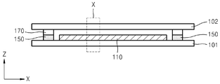
도 1은 본 발명의 일 실시예에 관한 평판 표시 장치를 도시한 개략적인 평면도이다.
도 2는 도 1의 Ⅱ-Ⅱ선을 따라 절취한 단면도이다.
도 3은 도 2의 X의 확대도이다.
도 4a 내지 도 4c는 도 1의 평판 표시 장치를 제조하는 과정 중 씰링 부재를 형성하는 단계를 순차적으로 도시한 개략적인 평면도들이다.
도 5는 본 발명의 다른 실시예에 관한 평판 표시 장치를 도시한 개략적인 평면도이다.
도 6a 내지 도 6d는 도 5의 평판 표시 장치를 제조하는 과정 중 씰링 부재를 형성하는 단계를 순차적으로 도시한 개략적인 평면도들이다.
도 7은 본 발명의 또 다른 실시예에 관한 평판 표시 장치를 도시한 개략적인 평면도이다.
도 8은 본 발명의 또 다른 실시예에 관한 평판 표시 장치를 도시한 개략적인 단면도이다.1 is a schematic plan view of a flat panel display device according to an exemplary embodiment of the present invention.
FIG. 2 is a cross-sectional view taken along the line II-II of FIG. 1.
3 is an enlarged view of X of FIG. 2.
4A through 4C are schematic plan views sequentially illustrating a step of forming a sealing member during a process of manufacturing the flat panel display of FIG. 1.
5 is a schematic plan view of a flat panel display device according to another exemplary embodiment of the present invention.
6A through 6D are schematic plan views sequentially illustrating a step of forming a sealing member during a process of manufacturing the flat panel display of FIG. 5.
7 is a schematic plan view of a flat panel display device according to still another exemplary embodiment of the present invention.
8 is a schematic cross-sectional view illustrating a flat panel display device according to still another exemplary embodiment of the present invention.
이하 첨부된 도면들에 도시된 본 발명에 관한 실시예를 참조하여 본 발명의 구성 및 작용을 상세히 설명한다.Hereinafter, with reference to the embodiments of the present invention shown in the accompanying drawings will be described in detail the configuration and operation of the present invention.
도 1은 본 발명의 일 실시예에 관한 평판 표시 장치를 도시한 개략적인 평면도이고, 도 2는 도 1의 Ⅱ-Ⅱ선을 따라 절취한 단면도이고, 도 3은 도 2의 X의 확대도이다. 1 is a schematic plan view of a flat panel display device according to an exemplary embodiment of the present invention, FIG. 2 is a cross-sectional view taken along the line II-II of FIG. 1, and FIG. 3 is an enlarged view of X of FIG. 2. .
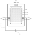
설명의 편의를 위하여 도 1에 밀봉 기판(102) 및 씰링 부재(170)은 도시하지 않았다. For convenience of description, the
평판 표시 장치(100)는 기판(101), 표시부(110), 밀봉 기판(102), 배선부(150), 씰링 부재(170) 및 제1, 2, 3 인입부 그룹(181, 182, 183)을 포함한다. The
제1 인입부 그룹(181)은 제1 부인입부A(181a) 및 제1 부인입부B(181b)를 포함하고, 제2 인입부 그룹(182)은 제2 부인입부A(182a) 및 제2 부인입부B(182b)를 포함하고, 제3 인입부 그룹(183)은 제3 부인입부A(183a) 및 제3 부인입부B(183b)를 포함한다.The
도 1 내지 도 3을 참조하면서 각 구성에 대하여 구체적으로 설명하기로 한다.Each configuration will be described in detail with reference to FIGS. 1 to 3.
기판(101)은 SiO2를 주성분으로 하는 투명한 유리 재질로 이루어질 수 있다. 기판(101)은 반드시 이에 한정되는 것은 아니며 투명한 플라스틱 재질로 형성할 수도 있다. 이 때 기판(101)을 형성하는 플라스틱 재질은 절연성 유기물인 폴리에테르술폰(PES, polyethersulphone), 폴리아크릴레이트(PAR, polyacrylate), 폴리에테르 이미드(PEI, polyetherimide), 폴리에틸렌 나프탈레이트(PEN, polyethyelenen napthalate), 폴리에틸렌 테레프탈레이드(PET, polyethyeleneterepthalate), 폴리페닐렌 설파이드(polyphenylene sulfide: PPS), 폴리아릴레이트(polyallylate), 폴리이미드(polyimide), 폴리카보네이트(PC), 셀룰로오스 트리 아세테이트(TAC), 셀룰로오스 아세테이트 프로피오네이트(cellulose acetate propionate: CAP)로 이루어진 그룹으로부터 선택되는 유기물일 수 있다.The
기판(101)상에 표시부(110)가 배치된다. 표시부(110)는 다양한 형태일 수 있다. 본 실시예에서는 표시부(110)가 유기 발광 소자(120)를 구비하고 있으나 본 발명은 이에 한정되지 않고 표시부(110)가 액정 소자를 구비할 수도 있다. The
표시부(110)에 대향하도록 밀봉 기판(102)이 배치된다. 기판(101)과 밀봉 기판(102)사이에는 씰링 부재(170)가 배치된다. 씰링 부재(170)는 표시부(110)를 둘러싸도록 형성된다. 씰링 부재(170)는 기판(101)과 밀봉 기판(102)이 결합하는 것을 용이하게 한다. 씰링 부재(170)는 프릿을 함유하는 것이 바람직하다.The
씰링 부재(170)와 중첩하도록 배선부(150)가 형성된다. 즉 배선부(150)는 표시부(110)를 둘러싸도록 형성된다. 기판(101)상에 배선부(150)가 형성되고, 배선부(150)상에 씰링 부재(170)가 형성되고, 씰링 부재(170)상에 밀봉 기판(102)이 배치된다.The
구체적으로 평판 표시 장치(100)의 제조 과정 중 씰링 부재(170)형성 시 씰링 부재(170)를 형성하기 위한 재료를 배치한 후 외부의 전원을 통하여 배선부(150)에 전압을 인가하여 배선부(150)에 줄열(joule heat)이 발생하고, 이러한 열에 의하여 씰링 부재(170)를 형성하기 위한 재료가 용융 및 경화되어 씰링 부재(170)가 최종적으로 형성된다.Specifically, when the sealing
배선부(150)는 모서리 부분이 각진 형태가 아닌 곡선을 갖도록 형성하는 것이 바람직하다. 이를 통하여 평판 표시 장치(100)를 제조하는 과정 중 씰링 부재(170)를 형성하기 위한 재료를 용융하기 위하여 전압을 인가 시 배선부(150)의 모서리 부분에서 비정상적으로 전압이 인가되는 것을 효과적으로 방지할 수 있다.The
배선부(150)의 폭은 씰링 부재(170)의 폭과 대응되거나 공정 조건에 따라 씰링 부재(170)의 폭보다 약간 작게 또는 약간 크게 할 수 있다.The width of the
배선부(150)와 연결되도록 제1, 2, 3 인입부 그룹(181, 182, 183)이 형성된다. First, second, and third lead-in
제1 인입부 그룹(181)은 제1 부인입부A(181a) 및 제1 부인입부B(181b)를 포함한다. 제1 부인입부A(181a) 및 제1 부인입부B(181b)는 배선부(150)와 연결되고, 제1 부인입부A(181a) 및 제1 부인입부B(181b)는 서로 이격된다. The
제1 부인입부A(181a) 및 제1 부인입부B(181b)는 배선부(150)보다 큰 폭을 갖도록 형성하는 것이 바람직하다. 이를 통하여 씰링 부재(170)를 형성 시 전압을 인가하는 단계에서 제1 부인입부A(181a) 및 제1 부인입부B(181b)가 비정상적으로 발열하는 것을 방지하고 배선부(150)에 안정적인 전압 인가가 용이하도록 한다.It is preferable that the first
제2 인입부 그룹(182)은 제2 부인입부A(182a) 및 제2 부인입부B(182b)를 포함한다. 제2 부인입부A(182a) 및 제2 부인입부B(182b)는 배선부(150)와 연결되고, 제2 부인입부A(182a) 및 제2 부인입부B(182b)는 서로 이격된다. The
제2 부인입부A(182a) 및 제2 부인입부B(182b)는 배선부(150)보다 큰 폭을 갖도록 형성하는 것이 바람직하다. 이를 통하여 씰링 부재(170)를 형성 시 전압을 인가하는 단계에서 제2 부인입부A(182a) 및 제2 부인입부B(182b)가 비정상적으로 발열하는 것을 방지하고 배선부(150)에 안정적인 전압 인가가 용이하도록 한다.It is preferable to form the second
제3 인입부 그룹(183)은 제3 부인입부A(183a) 및 제3 부인입부B(183b)를 포함한다. 제3 부인입부A(183a) 및 제3 부인입부B(183b)는 배선부(150)와 연결되고, 제3 부인입부A(183a) 및 제3 부인입부B(183b)는 서로 이격된다. The
제3 부인입부A(183a) 및 제3 부인입부B(183b)는 배선부(150)보다 큰 폭을 갖도록 형성하는 것이 바람직하다. 이를 통하여 씰링 부재(170)를 형성 시 전압을 인가하는 단계에서 제3 부인입부A(183a) 및 제3 부인입부B(183b)가 비정상적으로 발열하는 것을 방지하고 배선부(150)에 안정적인 전압 인가가 용이하도록 한다.It is preferable to form the 3rd
씰링 부재(170)를 형성하기 위한 공정 중 제1, 2, 3 인입부 그룹(181, 182, 183) 중 순차적으로 두 개의 인입부 그룹을 선택한 후 외부의 전원을 통하여 순차적으로 전압을 인가하게 된다. 배선부(150)의 전체 영역을 한번의 공정으로 전압을 인가하지 않고, 영역별로 나누어 복수 회의 공정을 통하여 전압을 인가하게 된다.During the process of forming the sealing
이를 통하여 배선부(150)의 전체 영역에서 전압 강하(IR drop)를 방지하여 균일한 씰링 부재(170)특성을 확보할 수 있다. 특히 각 인입부 그룹이 복수의 부인입부를 구비하므로 전압 인가 시 배선부(150)의 영역 중 비정상적으로 낮은 열이 발생하는 영역이 발생하는 것을 방지할 수 있다. 이에 대한 구체적인 내용은 도 4a 내지 도 4c를 참조하면서 후술하기로 한다.As a result, voltage drop (IR drop) may be prevented in the entire area of the
제1, 2, 3 인입부 그룹(181, 182, 183)은 외부의 전원(미도시)과 전기적으로 용이하게 연결될 수 있도록 기판(101)의 단부에 근접하도록 형성한다. The first, second, and third lead-in
제1, 2, 3 인입부 그룹(181, 182, 183)은 도전성 물질로 형성하는데 배선부(150)와 동일한 재료를 이용하여 형성할 수 있다.The first, second, and third lead-in
본 발명에서 표시부(110)는 다양한 형태일 수 있는데 본 실시예에서는 유기 발광 소자(120)를 적용한 표시부(110)가 개시된다. 도 3을 참조하면서 표시부(110)에 대하여 구체적으로 설명한다.In the present invention, the
기판(101)상에 버퍼층(111)이 형성된다. 버퍼층(111)은 기판(101)의 상부에 평탄한 면을 제공할 수 있고 기판(101)방향으로 수분 및 이물이 침투하는 것을 방지한다. The
버퍼층(111)상에 소정 패턴의 활성층(112)이 형성된다. 활성층(112)은 아모퍼스 실리콘 또는 폴리 실리콘과 같은 무기 반도체나 유기 반도체로 형성될 수 있고 소스 영역, 드레인 영역 및 채널 영역을 포함한다. The
소스 및 드레인 영역은 아모퍼스 실리콘 또는 폴리 실리콘으로 형성한 활성층(112)에 불순물을 도핑하여 형성할 수 있다. 3족 원소인 붕소(B)등으로 도핑하면 p-type, 5족 원소인 질소(N)등으로 도핑하면 n-type 반도체를 형성할 수 있다. The source and drain regions may be formed by doping impurities into the
활성층(112)의 상부에는 게이트 절연막(113)이 형성되고, 게이트 절연막(113)상부의 소정 영역에는 게이트 전극(114)이 형성된다. 게이트 절연막(113)은 활성층(112)과 게이트 전극(114)을 절연하기 위한 것으로 유기물 또는 SiNx, SiO2같은 무기물로 형성할 수 있다. The
게이트 전극(114)은 Au, Ag, Cu, Ni, Pt, Pd, Al, Mo, 또는 Al:Nd, Mo:W 합금 등과 같은 금속 또는 금속의 합금으로 이루어질 수 있으나 이에 한정되지 않고 밀착성, 평탄성, 전기 저항 및 가공성 등을 고려하여 다양한 재료를 사용할 수 있다. 게이트 전극(114)은 전기적 신호를 인가하는 게이트 라인(미도시)과 연결되어 있다. The
게이트 전극(114)의 상부로는 층간 절연막(115)이 형성된다. 층간 절연막(115) 및 게이트 절연막(113)은 활성층(112)의 소스 영역 및 드레인 영역을 노출하도록 형성되고 이러한 활성층(112)의 노출된 영역에 소스 전극(116) 및 드레인 전극(117)이 접하도록 형성한다. An interlayer insulating
소스 전극(116) 및 드레인 전극(117)을 이루는 물질은 Au, Pd, Pt, Ni, Rh, Ru, Ir, Os 외에도, Al, Mo, Al:Nd 합금, MoW 합금 등과 같은 2 종 이상의 금속으로 이루어진 합금을 사용할 수 있으며 이에 한정되지는 않는다. The material forming the
소스 전극(116) 및 드레인 전극(117)을 덮도록 패시베이션층(118)이 형성된다. 패시베이션층(118)은 무기 절연막 및/또는 유기 절연막을 사용할 수 있는데 무기 절연막으로는 SiO2, SiNx, SiON, Al2O3, TiO2, Ta2O5, HfO2, ZrO2, BST, PZT 등이 포함되도록 할 수 있고, 유기 절연막으로는 일반 범용고분자(PMMA, PS), phenol그룹을 갖는 고분자 유도체, 아크릴계 고분자, 이미드계 고분자, 아릴에테르계 고분자, 아마이드계 고분자, 불소계고분자, p-자일렌계 고분자, 비닐알콜계 고분자 및 이들의 블렌드 등이 포함되도록 할 수 있다. 패시베이션층(118)은 무기 절연막과 유기 절연막의 복합 적층체로도 형성될 수 있다.The
패시베이션층(118)은 드레인 전극(117)을 노출하도록 형성되고, 노출된 드레인 전극(117)과 연결되도록 유기 발광 소자(120)를 형성한다. 유기 발광 소자(120)는 제1 전극(121), 제2 전극(122) 및 중간층(123)을 포함한다. 구체적으로 제1 전극(121)과 드레인 전극(117)이 접촉한다. The
중간층(123)은 유기 발광층을 구비하고 제1 전극(121)과 제2 전극(122)을 통하여 전압이 인가되면 가시 광선을 구현한다. The
제1 전극(121)상에 절연물로 화소 정의막(119)(pixel define layer)을 형성한다. 화소 정의막(119)에 소정의 개구를 형성하여 제1 전극(121)이 노출되도록 한다. 노출된 제1 전극(121)상에 중간층(123)을 형성한다. 그리고, 중간층(123)과 연결되도록 제2 전극(122)을 형성한다.A pixel define
제1 전극(121), 제2 전극(122)은 각각 애노드 전극, 캐소드 전극의 극성을 갖도록 한다. 물론 제1 전극(121), 제2 전극(122)의 극성은 바뀔 수 있다.The
제2 전극(122)상에 밀봉 기판(102)이 배치된다. The
도 4a 내지 도 4c는 도 1의 평판 표시 장치(100)를 제조하는 과정 중 씰링 부재(170)를 형성하는 단계를 순차적으로 도시한 개략적인 평면도들이다. 구체적으로 도 4a 내지 도 4c는 씰링 부재(170)를 형성하기 위하여 외부의 전원을 통하여 순차적으로 전압을 인가하는 단계를 도시하고 있다.4A through 4C are schematic plan views sequentially illustrating a step of forming the sealing
도 1의 평판 표시 장치(100)를 제조하는 방법은 여러 공정을 포함하는데 그 중 씰링 부재(170)를 형성하는 단계를 포함한다. 씰링 부재(170)를 형성하는 단계는 씰링 부재(170)를 형성하기 위한 재료를 배치한 후 이것을 용융 및 경화시키기 위하여 배선부(150)에 전압을 인가하는 단계를 포함한다. The method of manufacturing the
먼저 도 4a를 참조하면 외부의 전원(190)의 양 단을 제1 인입부 그룹(181)의 제1 부인입부A(181a) 및 제2 인입부 그룹(182)의 제2 부인입부B(182b)에 연결한다. 그리고 나서 전압을 인가하면 배선부(150)의 영역 중 주로 제1 부인입부A(181a)와 제2 부인입부B(182b)사이에 배치된 배선부(150)의 영역에 줄열이 발생한다. 이를 통하여 배선부(150)와 중첩되도록 배치된 씰링 부재(170)의 재료가 용이하게 용융된 후 경화된다.First, referring to FIG. 4A, both ends of the
그리고 나서 도 4b를 참조하면 외부의 전원(190)의 양 단을 제2 인입부 그룹(182)의 제2 부인입부A(182a) 및 제3 인입부 그룹(183)의 제3 부인입부B(183b)에 연결한다. 그리고 나서 전압을 인가하면 배선부(150)의 영역 중 주로 제2 부인입부A(182a)와 제3 부인입부B(183b)사이에 배치된 배선부(150)의 영역에 줄열이 발생한다. 이를 통하여 배선부(150)와 중첩되도록 배치된 씰링 부재(170)의 재료가 용이하게 용융된 후 경화된다. 즉 복수 회의 전압 인가 시 전압이 배선부(150)의 소정의 영역에는 전압이 복수 회 인가되고 이를 통하여 씰링 부재(170)에 충분히 열이 공급되어 완전히 용융후 경화된다.4B, both ends of the
특히 전술한대로 도 4a에서는 제2 부인입부B(182b)에 전원(190)을 연결하고 도 4b에서는 제2 부인입부A(182a)에 전원(190)을 연결하여 배선부(150)의 영역 중 제2 부인입부A(182a), 제2 부인입부B(182b) 및 제2 부인입부A(182a)와 제2 부인입부B(182b) 사이에 대응하는 배선부(150)의 영역에 충분히 전압이 인가되어 씰링 부재(170)를 형성하기 위한 재료가 비정상적으로 덜 용융되는 것을 방지한다.In particular, as described above, in FIG. 4A, the
그리고 나서 도 4c를 참조하면 외부의 전원(190)의 양 단을 제3 인입부 그룹(183)의 제3 부인입부A(183a) 및 제1 인입부 그룹(181)의 제1 부인입부B(181b)에 연결한다. 그리고 나서 전압을 인가하면 배선부(150)의 영역 중 주로 제3 부인입부A(183a)와 제1 부인입부B(181b)사이에 배치된 배선부(150)의 영역에 줄열이 발생한다. 이를 통하여 배선부(150)와 중첩되도록 배치된 씰링 부재(170)의 재료가 용이하게 용융된 후 경화된다.Then, referring to FIG. 4C, both ends of the
특히 전술한대로 도 4b에서는 제3 부인입부B(183b)에 전원(190)을 연결하고 도 4c에서는 제3 부인입부A(183a)에 전원(190)을 연결하여 배선부(150)의 영역 중 제3 부인입부A(183a), 제3 부인입부B(183b) 및 제3 부인입부A(183a)와 제3 부인입부B(183b) 사이에 대응하는 배선부(150)의 영역에 충분히 전압이 인가되어 씰링 부재(170)를 형성하기 위한 재료가 덜 용융되는 것을 방지한다. In particular, as described above, in FIG. 4B, the
또한 도 4a에서는 제1 부인입부A(181a)에 전원(190)을 연결하고 도 4c에서는 제1 부인입부B(181b)에 전원(190)을 연결하여 배선부(150)의 영역 중 제1 부인입부A(181a), 제1 부인입부B(181b) 및 제1 부인입부A(181a)와 제1 부인입부B(181b) 사이에 대응하는 배선부(150)의 영역에 충분히 전압이 인가되어 씰링 부재(170)를 형성하기 위한 재료가 덜 용융되는 것을 방지한다.In addition, in FIG. 4A, the
배선부(150)에 전압을 인가 시 배선부(150)가 길게 형성되므로 배선부(150)의 영역 중 전압 강하(IR drop)가 발생하는 부분이 존재하고 그로 인하여 씰링 부재(170)를 형성하기 위한 재료가 불균일하게 용융되어 결과적으로 씰링 부재(170)가 불균일한 특성을 갖게될 수 있다. 그러나 본 발명은 세 개의 인입부 그룹(181, 182, 183)을 포함하고 이들 중 두 개씩 순차적으로 선택하여 전압을 인가하므로 배선부(150)의 전체 영역에서 전압 강하(IR drop)가 발생하는 것을 방지하고, 배선부(150)의 전체 영역에 걸쳐 균일한 줄열이 발생하도록 한다. 이를 통하여 씰링 부재(170)를 형성하기 위한 재료가 균일하게 용융 및 경화되어 씰링 부재(170)가 균일한 특성을 갖는다. 결과적으로 기판(101)과 밀봉 기판(102)의 결합을 용이하게 하고 평판 표시 장치(100)의 봉지 특성을 향상한다.When the voltage is applied to the
도 5는 본 발명의 다른 실시예에 관한 평판 표시 장치를 도시한 개략적인 평면도이다. 설명의 편의를 위하여 도 5에 밀봉 기판(미도시) 및 씰링 부재(미도시)은 도시하지 않았고 전술한 실시예와 상이한 점을 중심으로 설명하기로 한다.5 is a schematic plan view of a flat panel display device according to another exemplary embodiment of the present invention. For convenience of description, the sealing substrate (not shown) and the sealing member (not shown) are not shown in FIG. 5 and will be described based on differences from the above-described embodiment.
평판 표시 장치(200)는 기판(201), 표시부(210), 밀봉 기판(미도시), 배선부(250), 씰링 부재(미도시) 및 제1, 2, 3, 4 인입부 그룹(281, 282, 283, 284)을 포함한다. The
도 5를 참조하면서 각 구성에 대하여 구체적으로 설명하기로 한다.With reference to FIG. 5, each structure is demonstrated concretely.
기판(201)상에 표시부(210)가 배치된다. 표시부(210)에 대향하도록 밀봉 기판(미도시)이 배치된다. 기판(201)과 밀봉 기판(미도시)사이에는 씰링 부재(미도시)가 배치된다. 씰링 부재(미도시)는 표시부(210)를 둘러싸도록 형성된다. 씰링 부재(미도시)는 기판(201)과 밀봉 기판(미도시)이 결합하는 것을 용이하게 한다. 씰링 부재(미도시)는 프릿을 함유하는 것이 바람직하다.The
씰링 부재(미도시)와 중첩하도록 배선부(250)가 형성된다. 즉 배선부(250)는 표시부(210)를 둘러싸도록 형성된다. 기판(201)상에 배선부(250)가 형성되고, 배선부(250)상에 씰링 부재(미도시)가 형성되고, 씰링 부재(미도시)상에 밀봉 기판(미도시)이 배치된다.The
배선부(250)와 연결되도록 제1, 2, 3, 4 인입부 그룹(281, 282, 283, 284)이 형성된다. First, second, third, and fourth lead-in
제1 인입부 그룹(281)은 제1 부인입부A(281a) 및 제1 부인입부B(281b)를 포함한다. 제1 부인입부A(281a) 및 제1 부인입부B(281b)는 배선부(250)와 연결되고, 제1 부인입부A(281a) 및 제1 부인입부B(281b)는 서로 이격된다. 제1 부인입부A(281a) 및 제1 부인입부B(281b)는 배선부(250)보다 큰 폭을 갖도록 형성하는 것이 바람직하다.The
제2 인입부 그룹(282)은 제2 부인입부A(282a) 및 제2 부인입부B(282b)를 포함한다. 제2 부인입부A(282a) 및 제2 부인입부B(282b)는 배선부(250)와 연결되고, 제2 부인입부A(282a) 및 제2 부인입부B(282b)는 서로 이격된다. 제2 부인입부A(282a) 및 제2 부인입부B(282b)는 배선부(250)보다 큰 폭을 갖도록 형성하는 것이 바람직하다. The
제3 인입부 그룹(283)은 제3 부인입부A(283a) 및 제3 부인입부B(283b)를 포함한다. 제3 부인입부A(283a) 및 제3 부인입부B(283b)는 배선부(250)와 연결되고, 제3 부인입부A(283a) 및 제3 부인입부B(283b)는 서로 이격된다. 제3 부인입부A(283a) 및 제3 부인입부B(283b)는 배선부(250)보다 큰 폭을 갖도록 형성하는 것이 바람직하다.The
제4 인입부 그룹(284)은 제4 부인입부A(284a) 및 제4 부인입부B(284b)를 포함한다. 제4 부인입부A(284a) 및 제4 부인입부B(284b)는 배선부(250)와 연결되고, 제4 부인입부A(284a) 및 제4 부인입부B(284b)는 서로 이격된다. 제4 부인입부A(284a) 및 제4 부인입부B(284b)는 배선부(250)보다 큰 폭을 갖도록 형성하는 것이 바람직하다.The
씰링 부재(미도시)를 형성하기 위한 공정 중 제1, 2, 3, 4 인입부 그룹(281, 282, 283, 284) 중 순차적으로 두 개의 인입부 그룹을 선택한 후 외부의 전원을 통하여 순차적으로 전압을 인가하게 된다. 이를 통하여 배선부(250)의 전체 영역에서 전압 강하(IR drop)를 방지하여 균일한 씰링 부재(미도시)특성을 확보할 수 있다. 특히 각 인입부 그룹이 복수의 부인입부를 구비하므로 전압 인가 시 배선부(250)의 영역 중 비정상적으로 낮은 열이 발생하는 영역이 발생하는 것을 방지할 수 있다. 이에 대한 구체적인 내용은 도 6a 내지 도 6d를 참조하면서 후술하기로 한다.During the process of forming a sealing member (not shown), two inlet groups are sequentially selected from among the first, second, third, and
제1, 2, 3, 4 인입부 그룹(281, 282, 283, 284)은 외부의 전원(미도시)과 전기적으로 용이하게 연결될 수 있도록 기판(201)의 단부에 근접하도록 형성한다. The first, second, third, and fourth lead-in
제1, 2, 3, 4 인입부 그룹(281, 282, 283, 284)은 도전성 물질로 형성하는데 배선부(250)와 동일한 재료를 이용하여 형성할 수 있다.The first, second, third, and fourth lead-in
본 발명에서 표시부(210)는 다양한 형태일 수 있는데 유기 발광 소자 또는 액정 소자일 수 있다.In the present invention, the
도 6a 내지 도 6d는 도 5의 평판 표시 장치(200)를 제조하는 과정 중 씰링 부재(미도시)를 형성하는 단계를 순차적으로 도시한 개략적인 평면도들이다. 구체적으로 도 6a 내지 도 6d는 씰링 부재(미도시)를 형성하기 위하여 외부의 전원을 통하여 전압을 인가하는 단계를 도시하고 있다.6A through 6D are schematic plan views sequentially illustrating a step of forming a sealing member (not shown) during the manufacturing of the
도 5의 평판 표시 장치(200)를 제조하는 방법은 여러 공정을 포함하는데 그 중 씰링 부재(미도시)를 형성하는 단계를 포함한다. 씰링 부재(미도시)를 형성하는 단계는 씰링 부재(미도시)를 형성하기 위한 재료를 배치한 후 이것을 용융 및 경화시키기 위하여 배선부(250)에 전압을 인가하는 단계를 포함한다. The method of manufacturing the
먼저 도 6a를 참조하면 외부의 전원(290)의 양 단을 제1 인입부 그룹(281)의 제1 부인입부A(281a) 및 제2 인입부 그룹(282)의 제2 부인입부B(282b)에 연결한다. 그리고 나서 전압을 인가하면 배선부(250)의 영역 중 주로 제1 부인입부A(281a)와 제2 부인입부B(282b)사이에 배치된 배선부(250)의 영역에 줄열이 발생한다. 이를 통하여 배선부(250)와 중첩되도록 배치된 씰링 부재(미도시)의 재료가 용이하게 용융된 후 경화된다.First, referring to FIG. 6A, both ends of the
그리고 나서 도 6b를 참조하면 외부의 전원(290)의 양 단을 제2 인입부 그룹(282)의 제2 부인입부A(282a) 및 제3 인입부 그룹(283)의 제3 부인입부B(283b)에 연결한다. 그리고 나서 전압을 인가하면 배선부(250)의 영역 중 주로 제2 부인입부A(282a)와 제3 부인입부B(283b)사이에 배치된 배선부(250)의 영역에 줄열이 발생한다. 이를 통하여 배선부(250)와 중첩되도록 배치된 씰링 부재(미도시)의 재료가 용이하게 용융된 후 경화된다.6B, both ends of the
특히 전술한대로 도 6a에서는 제2 부인입부B(282b)에 전원(290)을 연결하고 도 6b에서는 제2 부인입부A(282a)에 전원(290)을 연결하여 배선부(250)의 영역 중 제2 부인입부A(282a), 제2 부인입부B(282b) 및 제2 부인입부A(282a)와 제2 부인입부B(282b) 사이에 대응하는 배선부(250)의 영역에 충분히 전압이 인가되어 씰링 부재(미도시)를 형성하기 위한 재료가 덜 용융되는 것을 방지한다.In particular, as described above, in FIG. 6A, the
그리고 나서 도 6c를 참조하면 외부의 전원(290)의 양 단을 제3 인입부 그룹(283)의 제3 부인입부A(283a) 및 제4 인입부 그룹(284)의 제4 부인입부B(284b)에 연결한다. 그리고 나서 전압을 인가하면 배선부(250)의 영역 중 주로 제3 부인입부A(283a)와 제4 부인입부B(284b)사이에 배치된 배선부(250)의 영역에 줄열이 발생한다. 이를 통하여 배선부(250)와 중첩되도록 배치된 씰링 부재(미도시)의 재료가 용이하게 용융된 후 경화된다.Then, referring to FIG. 6C, both ends of the
특히 전술한대로 도 6b에서는 제3 부인입부B(283b)에 전원(290)을 연결하고 도 6c에서는 제3 부인입부A(283a)에 전원(290)을 연결하여 배선부(250)의 영역 중 제3 부인입부A(283a), 제3 부인입부B(283b) 및 제3 부인입부A(283a)와 제3 부인입부B(283b) 사이에 대응하는 배선부(250)의 영역에 충분히 전압이 인가되어 씰링 부재(미도시)를 형성하기 위한 재료가 덜 용융되는 것을 방지한다. In particular, as described above, in FIG. 6B, the
그리고 나서 도 6d를 참조하면 외부의 전원(290)의 양 단을 제4 인입부 그룹(284)의 제4 부인입부A(284a) 및 제1 인입부 그룹(281)의 제1 부인입부B(281b)에 연결한다. 그리고 나서 전압을 인가하면 배선부(250)의 영역 중 주로 제4 부인입부A(284a)와 제1 부인입부B(281b)사이에 배치된 배선부(250)의 영역에 줄열이 발생한다. 이를 통하여 배선부(250)와 중첩되도록 배치된 씰링 부재(미도시)의 재료가 용이하게 용융된 후 경화된다.6D, the both ends of the
특히 전술한대로 도 6c에서는 제4 부인입부B(284b)에 전원(290)을 연결하고 도 6d에서는 제4 부인입부A(284a)에 전원(290)을 연결하여 배선부(250)의 영역 중 제4 부인입부A(284a), 제4 부인입부B(284b) 및 제4 부인입부A(284a)와 제4 부인입부B(284b) 사이에 대응하는 배선부(250)의 영역에 충분히 전압이 인가되어 씰링 부재(미도시)를 형성하기 위한 재료가 덜 용융되는 것을 방지한다. In particular, as described above, in FIG. 6C, the
또한 도 6a에서는 제1 부인입부A(281a)에 전원(190)을 연결하고 도 6d에서는 제1 부인입부B(281b)에 전원(290)을 연결하여 배선부(250)의 영역 중 제1 부인입부A(281a), 제1 부인입부B(281b) 및 제1 부인입부A(281a)와 제1 부인입부B(281b) 사이에 대응하는 배선부(250)의 영역에 충분히 전압이 인가되어 줄열이 발생하여 씰링 부재(미도시)를 형성하기 위한 재료가 덜 용융되는 것을 방지한다.In addition, in FIG. 6A, the
배선부(250)에 전압을 인가 시 배선부(250)가 길게 형성되므로 배선부(250)의 영역 중 전압 강하(IR drop)가 발생하는 부분이 존재하고 그로 인하여 씰링 부재(미도시)를 형성하기 위한 재료가 불균일하게 용융되어 결과적으로 씰링 부재(미도시)가 불균일한 특성을 갖게될 수 있다. 그러나 본 발명은 네 개의 인입부 그룹(281, 282, 283, 284)을 포함하고 이들 중 두 개씩 순차적으로 선택하여 전압을 인가하므로 배선부(250)의 전체 영역에서 전압 강하(IR drop)가 발생하는 것을 방지하고, 배선부(250)의 전체 영역에 걸쳐 균일한 줄열이 발생하도록 한다. 이를 통하여 씰링 부재(미도시)를 형성하기 위한 재료가 균일하게 용융 및 경화되어 씰링 부재(미도시)가 균일한 특성을 갖는다. 결과적으로 기판(201)과 밀봉 기판(미도시)의 결합을 용이하게 하고 평판 표시 장치(200)의 봉지 특성을 향상한다.When the voltage is applied to the
도 7은 본 발명의 또 다른 실시예에 관한 평판 표시 장치를 도시한 개략적인 평면도이다. 설명의 편의를 위하여 도 7에 밀봉 기판(미도시) 및 씰링 부재(미도시)은 도시하지 않았고 전술한 실시예와 상이한 점을 중심으로 설명하기로 한다.7 is a schematic plan view of a flat panel display device according to still another exemplary embodiment of the present invention. For convenience of description, the sealing substrate (not shown) and the sealing member (not shown) are not shown in FIG. 7 and will be described based on differences from the above-described embodiment.
평판 표시 장치(300)는 기판(301), 표시부(310), 밀봉 기판(미도시), 배선부(350), 씰링 부재(미도시) 및 제1, 2, 3, 4, 5, 6 인입부 그룹(381, 382, 383, 384, 385, 386)을 포함한다. The
도 7을 참조하면서 각 구성에 대하여 구체적으로 설명하기로 한다.Each configuration will be described in detail with reference to FIG. 7.
기판(301)상에 표시부(310)가 배치된다. 표시부(310)에 대향하도록 밀봉 기판(미도시)이 배치된다. 기판(301)과 밀봉 기판(미도시)사이에는 씰링 부재(미도시)가 배치된다. 씰링 부재(미도시)는 표시부(310)를 둘러싸도록 형성된다. 씰링 부재(미도시)는 기판(301)과 밀봉 기판(미도시)이 결합하는 것을 용이하게 한다. 씰링 부재(미도시)는 프릿을 함유하는 것이 바람직하다.The
씰링 부재(미도시)와 중첩하도록 배선부(350)가 형성된다. 즉 배선부(350)는 표시부(310)를 둘러싸도록 형성된다. 기판(301)상에 배선부(350)가 형성되고, 배선부(350)상에 씰링 부재(미도시)가 형성되고, 씰링 부재(미도시)상에 밀봉 기판(미도시)이 배치된다.The
배선부(350)와 연결되도록 제1, 2, 3, 4, 5, 6 인입부 그룹(381, 382, 383, 384, 385, 386)이 형성된다. First, second, third, fourth, fifth, and sixth
제1 인입부 그룹(381)은 제1 부인입부A(381a) 및 제1 부인입부B(381b)를 포함한다. 제1 부인입부A(381a) 및 제1 부인입부B(381b)는 배선부(350)와 연결되고, 제1 부인입부A(381a) 및 제1 부인입부B(381b)는 서로 이격된다. 제1 부인입부A(381a) 및 제1 부인입부B(381b)는 배선부(350)보다 큰 폭을 갖도록 형성하는 것이 바람직하다.The
제2 인입부 그룹(382)은 제2 부인입부A(382a) 및 제2 부인입부B(382b)를 포함한다. 제2 부인입부A(382a) 및 제2 부인입부B(382b)는 배선부(350)와 연결되고, 제2 부인입부A(382a) 및 제2 부인입부B(382b)는 서로 이격된다. 제2 부인입부A(382a) 및 제2 부인입부B(382b)는 배선부(350)보다 큰 폭을 갖도록 형성하는 것이 바람직하다. The
제3 인입부 그룹(383)은 제3 부인입부A(383a) 및 제3 부인입부B(383b)를 포함한다. 제3 부인입부A(383a) 및 제3 부인입부B(383b)는 배선부(350)와 연결되고, 제3 부인입부A(383a) 및 제3 부인입부B(383b)는 서로 이격된다. 제3 부인입부A(383a) 및 제3 부인입부B(383b)는 배선부(350)보다 큰 폭을 갖도록 형성하는 것이 바람직하다.The
제4 인입부 그룹(384)은 제4 부인입부A(384a) 및 제4 부인입부B(384b)를 포함한다. 제4 부인입부A(384a) 및 제4 부인입부B(384b)는 배선부(350)와 연결되고, 제4 부인입부A(384a) 및 제4 부인입부B(384b)는 서로 이격된다. 제4 부인입부A(384a) 및 제4 부인입부B(384b)는 배선부(350)보다 큰 폭을 갖도록 형성하는 것이 바람직하다.The
제5 인입부 그룹(385)은 제5 부인입부A(385a) 및 제5 부인입부B(385b)를 포함한다. 제5 부인입부A(385a) 및 제5 부인입부B(385b)는 배선부(350)와 연결되고, 제5 부인입부A(385a) 및 제5 부인입부B(385b)는 서로 이격된다. 제5 부인입부A(385a) 및 제5 부인입부B(385b)는 배선부(350)보다 큰 폭을 갖도록 형성하는 것이 바람직하다.The
제6 인입부 그룹(386)은 제6 부인입부A(386a) 및 제6 부인입부B(386b)를 포함한다. 제6 부인입부A(386a) 및 제6 부인입부B(386b)는 배선부(350)와 연결되고, 제6 부인입부A(386a) 및 제6 부인입부B(386b)는 서로 이격된다. 제6 부인입부A(386a) 및 제6 부인입부B(386b)는 배선부(350)보다 큰 폭을 갖도록 형성하는 것이 바람직하다.The
씰링 부재(미도시)를 형성하기 위한 공정 중 제1, 2, 3, 4, 5, 6 인입부 그룹(381, 382, 383, 384, 385, 386) 중 순차적으로 두 개의 인입부 그룹을 선택한 후 외부의 전원을 통하여 순차적으로 전압을 인가하게 된다. 이를 통하여 배선부(350)의 전체 영역에서 전압 강하(IR drop)를 방지하여 균일한 씰링 부재(미도시)특성을 확보할 수 있다. 특히 각 인입부 그룹이 복수의 부인입부를 구비하므로 전압 인가 시 배선부(350)의 영역 중 비정상적으로 낮은 열이 발생하는 영역이 발생하는 것을 방지할 수 있다. During the process of forming a sealing member (not shown), two inlet groups are sequentially selected from among the first, second, third, fourth, fifth, and
제1, 2, 3, 4, 5, 6 인입부 그룹(381, 382, 383, 384, 385, 386)은 외부의 전원(미도시)과 전기적으로 용이하게 연결될 수 있도록 기판(301)의 단부에 근접하도록 형성한다. The first, second, second, third, fourth, fifth, and
제1, 2, 3, 4, 5, 6 인입부 그룹(381, 382, 383, 384, 385, 386)은 도전성 물질로 형성하는데 배선부(350)와 동일한 재료를 이용하여 형성할 수 있다.The first, second, third, fourth, fifth, and
본 발명에서 표시부(310)는 다양한 형태일 수 있는데 유기 발광 소자 또는 액정 소자일 수 있다.In the present invention, the
도시하지 않았으나 도 7의 평판 표시 장치(300)를 제조하는 과정 중 씰링 부재(미도시)를 형성하기 위하여 외부의 전원을 통하여 전압을 인가하는 단계도 전술한 실시예들과 유사하다.Although not shown, applying a voltage through an external power source to form a sealing member (not shown) during the manufacturing of the
즉 씰링 부재(미도시)를 형성하기 위한 재료를 배치한 후 이것을 용융 및 경화시키기 위하여 배선부(350)에 전압을 인가하기 위하여 6회의 전압 인가 공정을 거칠 수 있다. That is, after disposing a material for forming a sealing member (not shown), six voltage application processes may be performed to apply a voltage to the
구체적으로 먼저 외부의 전원(미도시)의 양 단을 제1 인입부 그룹(381)의 제1 부인입부A(381a) 및 제2 인입부 그룹(382)의 제2 부인입부B(382b)에 연결하여 전압을 인가하고, 그리고 나서 외부의 전원(미도시)의 양 단을 제2 인입부 그룹(382)의 제2 부인입부A(382a) 및 제3 인입부 그룹(383)의 제3 부인입부B(383b)에 연결하여 전압을 인가하고, 그리고 나서 외부의 전원(미도시)의 양 단을 제3 인입부 그룹(383)의 제3 부인입부A(383a) 및 제4 인입부 그룹(384)의 제4 부인입부B(384b)에 연결하여 전압을 인가하고, 그리고 나서 외부의 전원(미도시)의 양 단을 제4 인입부 그룹(384)의 제4 부인입부A(384a) 및 제5 인입부 그룹(385)의 제5 부인입부B(385b)에 연결하여 전압을 인가하고, 그리고 나서 외부의 전원(미도시)의 양 단을 제5 인입부 그룹(385)의 제5 부인입부A(385a) 및 제6 인입부 그룹(386)의 제6 부인입부B(386b)에 연결하여 전압을 인가하고, 그리고 나서 외부의 전원(미도시)의 양 단을 제6 인입부 그룹(386)의 제6 부인입부A(386a) 및 제1 인입부 그룹(381)의 제1 부인입부B(381b)에 연결하여 전압을 인가한다.Specifically, first, both ends of an external power source (not shown) are connected to the
도 8은 본 발명의 또 다른 실시예에 관한 평판 표시 장치를 도시한 개략적인 평면도이다. 8 is a schematic plan view of a flat panel display device according to still another exemplary embodiment of the present invention.
본 실시예의 평판 표시 장치(400)는 전술한 실시예들과 비교할 때 배선부(450)의 구성만 상이하므로 설명의 편의를 위하여 전술한 실시예와 상이한 점을 중심으로 설명하기로 한다.Since the flat
평판 표시 장치(400)는 기판(401), 표시부(410), 밀봉 기판(402), 배선부(450), 씰링 부재(470) 및 복수의 인입부 그룹(미도시)을 포함한다. 도시하지 않았으나 본 실시예의 평판 표시 장치(400)의 인입부 그룹(미도시)는 도 1, 5, 7에 도시된 인입부 그룹 중 어느 하나와 동일하다.The flat
도 8을 참조하면서 각 구성에 대하여 구체적으로 설명하기로 한다.Each configuration will be described in detail with reference to FIG. 8.
기판(401)상에 표시부(410)가 배치된다. 표시부(410)에 대향하도록 밀봉 기판(402)이 배치된다. 기판(401)과 밀봉 기판(402)사이에는 씰링 부재(470)가 배치된다. 씰링 부재(470)는 표시부(410)를 둘러싸도록 형성된다. 씰링 부재(470)는 기판(401)과 밀봉 기판(402)이 결합하는 것을 용이하게 한다. 씰링 부재(407)는 프릿을 함유하는 것이 바람직하다.The
배선부(450)는 복수의 배선 부재(451)를 구비한다. 복수의 배선 부재(451)는 씰링 부재(470)와 중첩되는 영역 중 적어도 일 영역에서 서로 이격된다. 배선 부재(451)들은 기판(401)상에 배치되고, 배선 부재(451)의 상부 및 각 배선 부재(451)들간의 이격된 공간에 씰링 부재(470)가 배치되고, 씰링 부재(470)상에 밀봉 기판(402)이 배치된다. The
씰링 부재(470)가 배선 부재(451)들간의 이격된 공간을 통하여 기판(401)과 접하므로 씰링 부재(470)의 내구성 및 기판(401)과 밀봉 기판(402)의 결합 특성이 향상된다.Since the sealing
배선부(450)의 배선 부재(451)에 대하여 구체적으로 설명하기로 한다. 씰링 부재(470)형성 시 씰링 부재(470)를 형성하기 위한 재료를 배치한 후 외부의 전원을 통하여 배선부(450)에 전압을 인가하여 배선부(450)에서 줄열(joule heat)이 발생하면 발생한 열에 의하여 재료가 용융된 후 경화되어 씰링 부재(470)가 최종적으로 형성된다. The
이 때 본 실시예의 배선부(450)는 복수의 배선 부재(451)를 구비하므로 전압이 인가될 때 씰링 부재(470)의 폭을 기준으로 중심과 주변의 온도 불균형을 방지할 수 있다. In this case, since the
또한 배선부(450)는 복수의 배선 부재(451)를 포함하여 배선부(450)의 모서리 부분에서 안쪽과 바깥쪽의 불균일한 전류 집중이 발생하지 않는다. 구체적으로 배선부(450)의 모서리 영역 중 표시부(410)와 가까운 내측에서 전류가 집중되는 것을 방지하여 전압 인가 시 배선부(450)의 전체 영역에서 전류가 균일하게 흐르도록 할 수 있다. 이를 통하여 씰링 부재(470)가 균일하게 가열되게 할 수 있다.In addition, the
도시하지 않았으나 복수의 인입부 그룹의 구성은 전술한 실시예들과 동일하므로 구체적인 설명은 생략한다. 또한 본 실시예의 평판 표시 장치(400)를 제조하는 과정 중 씰링 부재(470)를 형성하기 위하여 외부의 전원을 통하여 전압을 인가하는 단계도 전술한 실시예들과 유사하므로 구체적인 설명은 생략한다. Although not shown, the configuration of the plurality of inlet groups is the same as the above-described embodiments, and thus a detailed description thereof will be omitted. In addition, the step of applying a voltage through an external power source to form the sealing
전술한 실시예들에서는 세 개, 네 개 및 여섯 개의 인입부 그룹이 구비된 평판 표시 장치만을 설명하였으나 본 발명은 이에 한정되지 않는다. 세 개 이상의 인입부 그룹을 구비하되 평판 표시 장치의 크기 및 공정 조건에 따라서 인입부 그룹의 수를 달리할 수 있다. 또한 각 인입부 그룹에 구비된 부인입부를 두 개인 경우만 도시하였으나 복수의 전압 인가 공정 진행 시 배선부의 영역 중 전압이 복수 회 인가되는 부분이 존재하도록 각 인입부 그룹이 세 개 이상의 부인입부를 구비할 수도 있다. In the above-described embodiments, only the flat panel display device including three, four, and six lead groups is described, but the present invention is not limited thereto. Three or more inlet groups may be provided, but the number of inlet groups may vary according to the size and process conditions of the flat panel display. In addition, although only two non-entrance portions provided in each entry portion group are shown, each entry group includes three or more non-entrance portions so that a portion in which the voltage is applied a plurality of times exists in the area of the wiring portion during the process of applying a plurality of voltages. You may.
본 발명은 도면에 도시된 실시예를 참고로 설명되었으나 이는 예시적인 것에 불과하며, 당해 기술 분야에서 통상의 지식을 가진 자라면 이로부터 다양한 변형 및 균등한 다른 실시예가 가능하다는 점을 이해할 것이다. 따라서, 본 발명의 진정한 기술적 보호 범위는 첨부된 특허청구범위의 기술적 사상에 의하여 정해져야 할 것이다.Although the present invention has been described with reference to the embodiments shown in the drawings, these are merely exemplary, and those skilled in the art will understand that various modifications and equivalent other embodiments are possible. Therefore, the true technical protection scope of the present invention will be defined by the technical spirit of the appended claims.
100, 200, 300, 400: 평판 표시 장치
101, 201, 301, 401: 기판
110, 210, 310, 410: 표시부
150, 250, 350, 450: 배선부
170, 470: 씰링 부재
181, 182, 183, 281, 282, 283, 284, 381,382, 383, 384, 385, 386: 인입부 그룹
181a, 181b, 182a, 182b, 183a, 183b, 281a, 281b, 282a, 282b, 283a, 283b, 284a, 284b, 381a, 381b, 382a, 382b, 383a, 383b, 384a, 383b, 385a, 385b, 386a, 386b: 부인입부
190, 290, 390: 전원100, 200, 300, 400: flat panel display
101, 201, 301, 401: substrate
110, 210, 310, 410: display unit
150, 250, 350, 450: wiring section
170, 470: sealing member
181, 182, 183, 281, 282, 283, 284, 381,382, 383, 384, 385, 386: entry group
181a, 181b, 182a, 182b, 183a, 183b, 281a, 281b, 282a, 282b, 283a, 283b, 284a, 284b, 381a, 381b, 382a, 382b, 383a, 383b, 384a, 383b, 385a, 385b, 386b,
190, 290, 390: power
Claims (20)
상기 기판 상에 배치되는 표시부;
상기 표시부와 대향하도록 배치된 밀봉 기판;
상기 기판과 상기 밀봉 기판 사이에 상기 표시부를 둘러싸도록 배치되는 씰링 부재;
상기 기판과 상기 밀봉 기판 사이에 상기 씰링 부재와 중첩되는 영역을 구비하도록 배치되는 배선부; 및
외부의 전원을 통하여 전압을 인가받을 수 있도록 형성되고 상기 배선부와 연결되는 세 개 이상의 인입부 그룹을 포함하고,
상기 각 인입부 그룹은 복수의 부(副)인입부를 구비하는 평판 표시 장치.Board;
A display unit disposed on the substrate;
A sealing substrate disposed to face the display portion;
A sealing member disposed to surround the display unit between the substrate and the sealing substrate;
A wiring part disposed between the substrate and the sealing substrate to have a region overlapping with the sealing member; And
It includes three or more groups of lead portion is formed to receive a voltage through an external power source and connected to the wiring portion,
And each of the inlet portion groups includes a plurality of negative inlet portions.
상기 각 인입부 그룹에 구비된 상기 복수의 부인입부들은 서로 이격된 평판 표시 장치.The method according to claim 1,
The flat display device of claim 1, wherein the plurality of non-indentations provided in the inlet groups are spaced apart from each other.
상기 각 인입부 그룹은 서로 이격된 두개의 부인입부를 구비하는 평판 표시 장치.The method according to claim 1,
Each entry group includes two denier entries spaced apart from each other.
상기 부인입부의 폭은 상기 배선부의 폭보다 크도록 형성된 평판 표시 장치.The method according to claim 1,
And the width of the non-entrance portion is greater than the width of the wiring portion.
상기 인입부 그룹은 서로 이격되도록 순차적으로 배치되는 제1 인입부 그룹, 제2 인입부 그룹 및 제3 인입부 그룹을 포함하고,
상기 제1 인입부 그룹, 제2 인입부 그룹 및 제3 인입부 그룹은 각각 서로 이격되도록 배치된 두 개의 부인입부들을 구비하는 평판 표시 장치.The method according to claim 1,
The inlet group includes a first inlet group, a second inlet group, and a third inlet group, which are sequentially arranged to be spaced apart from each other,
The first inlet group, the second inlet group, and the third inlet group each include two non-indentations arranged to be spaced apart from each other.
상기 인입부 그룹은 서로 이격되도록 순차적으로 배치되는 제1 인입부 그룹, 제2 인입부 그룹, 제3 인입부 그룹 및 제4 인입부 그룹을 포함하고,
상기 제1 인입부 그룹, 제2 인입부 그룹, 제3 인입부 그룹 및 제4 인입부 그룹은 각각 서로 이격되도록 배치된 두 개의 부인입부들을 구비하는 평판 표시 장치.The method according to claim 1,
The inlet group includes a first inlet group, a second inlet group, a third inlet group, and a fourth inlet group, which are sequentially arranged to be spaced apart from each other,
The first inlet group, the second inlet group, the third inlet group, and the fourth inlet group each include two non-indentations disposed to be spaced apart from each other.
상기 인입부 그룹은 서로 이격되도록 순차적으로 배치되는 제1 인입부 그룹, 제2 인입부 그룹, 제3 인입부 그룹, 제4 인입부 그룹, 제5 인입부 그룹 및 제6 인입부 그룹을 포함하고,
상기 제1 인입부 그룹, 제2 인입부 그룹, 제3 인입부 그룹, 제4 인입부 그룹, 제5 인입부 그룹 및 제6 인입부 그룹은 각각 서로 이격되도록 배치된 두 개의 부인입부들을 구비하는 평판 표시 장치.The method according to claim 1,
The inlet group includes a first inlet group, a second inlet group, a third inlet group, a fourth inlet group, a fifth inlet group, and a sixth inlet group sequentially arranged to be spaced apart from each other. ,
The first inlet group, the second inlet group, the third inlet group, the fourth inlet group, the fifth inlet group, and the sixth inlet group each have two denier contacts spaced apart from each other. Flat panel display device.
상기 배선부는 복수의 배선 부재를 구비하는 평판 표시 장치.The method according to claim 1,
And the wiring portion includes a plurality of wiring members.
상기 배선 부재는 상기 씰링 부재와 중첩되는 영역 중 적어도 일 영역에서 서로 이격되도록 형성된 평판 표시 장치.The method of claim 8,
The wiring member is formed to be spaced apart from each other in at least one region of the region overlapping the sealing member.
상기 배선 부재는 상기 기판상에 형성되고, 상기 씰링 부재는 상기 배선 부재의 상부 및 상기 복수의 배선 부재 중 인접한 배선 부재들간의 이격된 공간에 배치되는 평판 표시 장치.The method of claim 8,
And the wiring member is formed on the substrate, and the sealing member is disposed in a space separated from an upper portion of the wiring member and adjacent wiring members among the plurality of wiring members.
상기 씰링 부재는 프릿을 함유하는 평판 표시 장치.The method according to claim 1,
And the sealing member contains a frit.
상기 표시부는 유기 발광 소자 또는 액정 표시 소자를 구비하는 평판 표시 장치.The method according to claim 1,
The display unit includes an organic light emitting element or a liquid crystal display element.
상기 표시부와 대향하도록 밀봉 기판을 배치하는 단계;
상기 기판과 상기 밀봉 기판 사이에 상기 표시부를 둘러싸는 씰링 부재를 형성하는 단계;
상기 기판과 상기 밀봉 기판 사이에 상기 씰링 부재와 중첩되는 영역을 구비하도록 배선부를 형성하는 단계; 및
외부의 전원과 전기적으로 연결될 수 있도록 배치되는 세 개 이상의 인입부그룹을 형성하는 단계를 포함하고,
상기 각 인입부 그룹은 상기 배선부와 연결되는 복수의 부인입부를 구비하고,
상기 씰링 부재를 형성하는 단계는 상기 씰링 부재를 형성하기 위한 재료를 상기 기판과 상기 밀봉 기판 사이에 배치하고 상기 인입부 그룹 중 인접한 두 개의 인입부 그룹을 순차적으로 선택하여 상기 선택된 두 개의 인입부 그룹에 상기 외부의 전원을 연결하여 전압을 순차적으로 인가하고, 상기 인입부 그룹을 통하여 인가된 전압을 통하여 상기 배선부에서 발생하는 열을 이용하여 상기 씰링 부재를 형성하기 위한 재료를 용융 후 경화하는 단계를 포함하는 평판 표시 장치 제조 방법.Preparing a substrate on which a display unit is disposed;
Arranging a sealing substrate to face the display unit;
Forming a sealing member surrounding the display unit between the substrate and the sealing substrate;
Forming a wiring portion between the substrate and the sealing substrate to have a region overlapping with the sealing member; And
Forming at least three lead groups arranged to be electrically connected to an external power source,
Each of the lead-in groups includes a plurality of non-inserted portions connected to the wiring portion,
The forming of the sealing member may include disposing a material for forming the sealing member between the substrate and the sealing substrate and sequentially selecting two adjacent inlet groups among the inlet groups to select the selected two inlet groups. Applying a voltage sequentially by connecting the external power source to the external power source, and hardening and curing the material for forming the sealing member by using heat generated in the wiring unit through the voltage applied through the lead-in group. Flat panel display manufacturing method comprising a.
상기 씰링 부재를 형성하는 단계는 상기 인입부 그룹 중 인접한 두 개의 인입부 그룹을 순차적으로 선택하고, 상기 선택된 두 개의 인입부 그룹은 일 인입부 그룹 및 다른 일 인입부 그룹을 구비하고,
상기 일 인입부 그룹의 부인입부들 중 상기 다른 일 인입부로부터 가장 가까운 부인입부를 제외한 부인입부들 중 하나의 부인입부 및 상기 다른 일 인입부 그룹의 부인입부들 중 상기 일 인입부로부터 가장 가까운 부인입부를 제외한 부인입부들 중 하나의 부인입부를 상기 외부의 전원에 연결하고 전압을 인가하는 단계를 구비하는 평판 표시 장치 제조 방법.The method of claim 13,
The forming of the sealing member may include sequentially selecting two adjacent inlet groups among the inlet groups, wherein the selected two inlet groups include one inlet group and another inlet group,
The denial of one of the deniers except the denier closest to the other one of the deniers of the one-entry group and the denier closest to the one-entry of the deniers of the other one-entry group A method of manufacturing a flat panel display device, the method comprising: connecting one non-entrant portion of the non-entrant portions to the external power source and applying a voltage.
상기 인입부 그룹은 서로 이격되도록 순차적으로 배치되는 제1 인입부 그룹, 제2 인입부 그룹 및 제3 인입부 그룹을 포함하고,
상기 제1 인입부 그룹은 상기 제3 인입부 그룹에 가깝게 배치되는 제1 부인입부A 및 상기 제1 부인입부A와 이격되고 상기 제2 인입부 그룹에 가깝게 배치되는 제1 부인입부B를 구비하고,
상기 제2 인입부 그룹은 상기 제1 인입부 그룹에 가깝게 배치되는 제2 부인입부A 및 상기 제2 부인입부A와 이격되고 상기 제3 인입부 그룹에 가깝게 배치되는 제2 부인입부B를 구비하고,
상기 제3 인입부 그룹은 상기 제2 인입부 그룹에 가깝게 배치되는 제3 부인입부A 및 상기 제3 부인입부A와 이격되고 상기 제1 인입부 그룹에 가깝게 배치되는 제3 부인입부B를 구비하고,
상기 씰링 부재를 형성하는 단계는 상기 제1 부인입부A 및 상기 제2 부인입부B에 상기 외부의 전원을 연결하여 전압을 인가하고 나서, 상기 제2 부인입부A 및 상기 제3 부인입부B에 상기 외부의 전원을 연결하여 전압을 인가하고 나서, 상기 제3 부인입부A 및 상기 제1 부인입부B에 상기 외부의 전원을 연결하여 전압을 인가하는 단계를 구비하는 평판 표시 장치 제조 방법.The method of claim 13,
The inlet group includes a first inlet group, a second inlet group, and a third inlet group, which are sequentially arranged to be spaced apart from each other,
The first inlet group includes a first non-adopted part A disposed close to the third inlet group and a first non-adopted part B spaced apart from the first inlet part A and disposed close to the second inlet part group; ,
The second inlet group has a second non-adopted part A disposed close to the first inlet group and a second non-adopted part B spaced apart from the second indented group A and disposed close to the third inlet group. ,
The third inlet group includes a third non-adopted part A disposed close to the second inlet group and a third non-adopted part B spaced apart from the third inlet part A and disposed close to the first inlet part group; ,
The forming of the sealing member may include connecting the external power to the first non-admission part A and the second non-admission part B and applying a voltage to the second non-admission part A and the third non-admission part B. Connecting an external power source to apply a voltage, and then connecting the external power source to the third non-admission part A and the first non-admission part B to apply a voltage.
상기 인입부 그룹은 서로 이격되도록 순차적으로 배치되는 제1 인입부 그룹, 제2 인입부 그룹, 제3 인입부 그룹 및 제4 인입부 그룹을 포함하고,
상기 제1 인입부 그룹은 상기 제4 인입부 그룹에 가깝게 배치되는 제1 부인입부A 및 상기 제1 부인입부A와 이격되고 상기 제2 인입부 그룹에 가깝게 배치되는 제1 부인입부B를 구비하고,
상기 제2 인입부 그룹은 상기 제1 인입부 그룹에 가깝게 배치되는 제2 부인입부A 및 상기 제2 부인입부A와 이격되고 상기 제3 인입부 그룹에 가깝게 배치되는 제2 부인입부B를 구비하고,
상기 제3 인입부 그룹은 상기 제2 인입부 그룹에 가깝게 배치되는 제3 부인입부A 및 상기 제3 부인입부A와 이격되고 상기 제4 인입부 그룹에 가깝게 배치되는 제3 부인입부B를 구비하고,
상기 제4 인입부 그룹은 상기 제3 인입부 그룹에 가깝게 배치되는 제4 부인입부A 및 상기 제4 부인입부A와 이격되고 상기 제1 인입부 그룹에 가깝게 배치되는 제4 부인입부B를 구비하고,
상기 씰링 부재를 형성하는 단계는 상기 제1 부인입부A 및 상기 제2 부인입부B에 상기 외부의 전원을 연결하여 전압을 인가하고 나서, 상기 제2 부인입부A 및 상기 제3 부인입부B에 상기 외부의 전원을 연결하여 전압을 인가하고 나서, 상기 제3 부인입부A 및 상기 제4 부인입부B에 상기 외부의 전원을 연결하여 전압을 인가하고 나서, 상기 제4 부인입부A 및 상기 제1 부인입부B에 상기 외부의 전원을 연결하여 전압을 인가하는 단계를 구비하는 평판 표시 장치 제조 방법.The method of claim 13,
The inlet group includes a first inlet group, a second inlet group, a third inlet group, and a fourth inlet group, which are sequentially arranged to be spaced apart from each other,
The first inlet group has a first non-adopted part A disposed close to the fourth inlet group and a first non-adopted part B spaced apart from the first inlet part A and disposed close to the second inlet part group; ,
The second inlet group has a second non-adopted part A disposed close to the first inlet group and a second non-adopted part B spaced apart from the second indented group A and disposed close to the third inlet group. ,
The third inlet group includes a third non-adopted part A disposed close to the second inlet group and a third non-adopted part B spaced apart from the third inlet part A and disposed close to the fourth inlet part group. ,
The fourth inlet group includes a fourth non-adopted part A disposed close to the third inlet group and a fourth non-adopted part B spaced apart from the fourth inlet part A and disposed close to the first inlet part group; ,
The forming of the sealing member may include connecting the external power to the first non-admission part A and the second non-admission part B and applying a voltage to the second non-admission part A and the third non-admission part B. After connecting an external power source to apply a voltage, and connecting the external power to the third non-admission part A and the fourth non-admission part B to apply a voltage, the fourth non-admission part A and the first denial And applying a voltage by connecting the external power source to the inlet B.
상기 인입부 그룹은 서로 이격되도록 순차적으로 배치되는 제1 인입부 그룹, 제2 인입부 그룹, 제3 인입부 그룹, 제4 인입부 그룹, 제5 인입부 그룹 및 제6 인입부 그룹을 포함하고,
상기 제1 인입부 그룹은 상기 제6 인입부 그룹에 가깝게 배치되는 제1 부인입부A 및 상기 제1 부인입부A와 이격되고 상기 제2 인입부 그룹에 가깝게 배치되는 제1 부인입부B를 구비하고,
상기 제2 인입부 그룹은 상기 제1 인입부 그룹에 가깝게 배치되는 제2 부인입부A 및 상기 제2 부인입부A와 이격되고 상기 제3 인입부 그룹에 가깝게 배치되는 제2 부인입부B를 구비하고,
상기 제3 인입부 그룹은 상기 제2 인입부 그룹에 가깝게 배치되는 제3 부인입부A 및 상기 제3 부인입부A와 이격되고 상기 제4 인입부 그룹에 가깝게 배치되는 제3 부인입부B를 구비하고,
상기 제4 인입부 그룹은 상기 제3 인입부 그룹에 가깝게 배치되는 제4 부인입부A 및 상기 제4 부인입부A와 이격되고 상기 제5 인입부 그룹에 가깝게 배치되는 제4 부인입부B를 구비하고,
상기 제5 인입부 그룹은 상기 제4 인입부 그룹에 가깝게 배치되는 제5 부인입부A 및 상기 제5 부인입부A와 이격되고 상기 제6 인입부 그룹에 가깝게 배치되는 제5 부인입부B를 구비하고,
상기 제6 인입부 그룹은 상기 제5 인입부 그룹에 가깝게 배치되는 제6 부인입부A 및 상기 제6 부인입부A와 이격되고 상기 제1 인입부 그룹에 가깝게 배치되는 제6 부인입부B를 구비하고,
상기 씰링 부재를 형성하는 단계는 상기 제1 부인입부A 및 상기 제2 부인입부B에 상기 외부의 전원을 연결하여 전압을 인가하고 나서, 상기 제2 부인입부A 및 상기 제3 부인입부B에 상기 외부의 전원을 연결하여 전압을 인가하고 나서, 상기 제3 부인입부A 및 상기 제4 부인입부B에 상기 외부의 전원을 연결하여 전압을 인가하고 나서, 상기 제4 부인입부A 및 상기 제5 부인입부B에 상기 외부의 전원을 연결하여 전압을 인가하고 나서, 상기 제5 부인입부A 및 상기 제6 부인입부B에 상기 외부의 전원을 연결하여 전압을 인가하고 나서, 상기 제6 부인입부A 및 상기 제1 부인입부B에 상기 외부의 전원을 연결하여 전압을 인가하는 단계를 구비하는 평판 표시 장치 제조 방법.The method of claim 13,
The inlet group includes a first inlet group, a second inlet group, a third inlet group, a fourth inlet group, a fifth inlet group, and a sixth inlet group sequentially arranged to be spaced apart from each other. ,
The first inlet group includes a first non-adopted part A disposed close to the sixth inlet group and a first non-adopted part B spaced apart from the first inlet part A and disposed close to the second inlet part group; ,
The second inlet group has a second non-adopted part A disposed close to the first inlet group and a second non-adopted part B spaced apart from the second indented group A and disposed close to the third inlet group. ,
The third inlet group includes a third non-adopted part A disposed close to the second inlet group and a third non-adopted part B spaced apart from the third inlet part A and disposed close to the fourth inlet part group. ,
The fourth inlet group includes a fourth non-adopted part A disposed close to the third inlet group and a fourth non-adopted part B spaced apart from the fourth inlet part A and disposed close to the fifth inlet part group; ,
The fifth inlet group includes a fifth non-adopted part A disposed close to the fourth inlet group and a fifth non-admitted part B spaced apart from the fifth indented part A and disposed close to the sixth inlet group; ,
The sixth inlet group has a sixth non-adopted part A disposed close to the fifth inlet group and a sixth non-admitted part B spaced apart from the sixth indented part A and disposed close to the first inlet part group; ,
The forming of the sealing member may include connecting the external power to the first non-admission part A and the second non-admission part B and applying a voltage to the second non-admission part A and the third non-admission part B. After connecting an external power source to apply a voltage, connecting the external power supply to the third non-admission part A and the fourth non-admission part B, and applying a voltage, the fourth non-admission part A and the fifth non-profit After the external power is connected to the inlet B, a voltage is applied, and after the external power is connected to the fifth non-adjacent A and the sixth non-adjacent B, the voltage is applied. And connecting a voltage to the first non-contact part B to apply a voltage.
상기 배선부는 상기 씰링 부재와 중첩되는 영역 중 적어도 일 영역에서 서로 이격되도록 형성된 복수의 배선 부재를 구비하도록 형성하는 평판 표시 장치 제조 방법.The method of claim 13,
And wherein the wiring portion includes a plurality of wiring members formed to be spaced apart from each other in at least one region of the region overlapping the sealing member.
상기 배선 부재는 상기 기판상에 형성하고, 상기 씰링 부재는 상기 배선 부재의 상부 및 상기 복수의 배선 부재 중 인접한 배선 부재들간의 이격된 공간에 형성하는 평판 표시 장치 제조 방법.The method of claim 18,
And the wiring member is formed on the substrate, and the sealing member is formed in a space separated from an upper portion of the wiring member and adjacent wiring members among the plurality of wiring members.
상기 씰링 부재는 프릿을 함유하는 평판 표시 장치 제조 방법.The method of claim 13,
And the sealing member contains a frit.
Priority Applications (2)
| Application Number | Priority Date | Filing Date | Title |
|---|---|---|---|
| KR1020100105376A KR20120044021A (en) | 2010-10-27 | 2010-10-27 | Flat panel display apparatus and method of manufacturing flat panel display apparatus |
| US13/236,854 US8564197B2 (en) | 2010-10-27 | 2011-09-20 | Flat panel display apparatus and method for manufacturing the same |
Applications Claiming Priority (1)
| Application Number | Priority Date | Filing Date | Title |
|---|---|---|---|
| KR1020100105376A KR20120044021A (en) | 2010-10-27 | 2010-10-27 | Flat panel display apparatus and method of manufacturing flat panel display apparatus |
Publications (1)
| Publication Number | Publication Date |
|---|---|
| KR20120044021A true KR20120044021A (en) | 2012-05-07 |
Family
ID=45996508
Family Applications (1)
| Application Number | Title | Priority Date | Filing Date |
|---|---|---|---|
| KR1020100105376A KR20120044021A (en) | 2010-10-27 | 2010-10-27 | Flat panel display apparatus and method of manufacturing flat panel display apparatus |
Country Status (2)
| Country | Link |
|---|---|
| US (1) | US8564197B2 (en) |
| KR (1) | KR20120044021A (en) |
Cited By (1)
| Publication number | Priority date | Publication date | Assignee | Title |
|---|---|---|---|---|
| US10109649B2 (en) | 2015-09-11 | 2018-10-23 | Samsung Display Co., Ltd. | Organic light-emitting display apparatus for improving an adhesion of a sealing member |
Families Citing this family (3)
| Publication number | Priority date | Publication date | Assignee | Title |
|---|---|---|---|---|
| KR102013893B1 (en) | 2012-08-20 | 2019-08-26 | 삼성디스플레이 주식회사 | Flat panel display device and method for fabricating the same |
| US20140078456A1 (en) * | 2012-09-19 | 2014-03-20 | Shenzhen China Star Optoelectronics Technology Co. Ltd. | Liquid Crystal Display Panel and Method for Making the Same |
| KR102439308B1 (en) * | 2015-10-06 | 2022-09-02 | 삼성디스플레이 주식회사 | Display apparutus |
Family Cites Families (11)
| Publication number | Priority date | Publication date | Assignee | Title |
|---|---|---|---|---|
| JP2000252058A (en) | 1999-03-01 | 2000-09-14 | Stanley Electric Co Ltd | Organic el display device and sealing method thereof |
| KR20010039300A (en) | 1999-10-29 | 2001-05-15 | 김영남 | Sealing method for field emission display |
| KR100337494B1 (en) | 2000-06-01 | 2002-05-24 | 박원석 | A Method For Fabricating An Organic Electro-Luminescence Display Panel Using A Glass Paste And An Organic Electro-Luminescence Display Panel Thereof |
| KR100429771B1 (en) | 2000-06-13 | 2004-05-03 | 권상직 | Method for the low temperature vacuum in-line frit sealing of flat panel display device using an auxiliary heat line |
| US7019718B2 (en) * | 2000-07-25 | 2006-03-28 | Semiconductor Energy Laboratory Co., Ltd. | Display device |
| KR20030080895A (en) | 2002-04-11 | 2003-10-17 | 엘지전자 주식회사 | Sealing method of organic electroluminescence device |
| KR100634887B1 (en) | 2004-09-24 | 2006-10-16 | 전자부품연구원 | OLED and method for fabricating the same |
| KR101085274B1 (en) | 2005-01-03 | 2011-11-22 | 사천홍시현시기건유한공사 | Method For encapsulating organic light emitting diode |
| KR101388585B1 (en) * | 2007-11-16 | 2014-04-23 | 삼성디스플레이 주식회사 | Organic light emitting display |
| US8067883B2 (en) | 2008-02-29 | 2011-11-29 | Corning Incorporated | Frit sealing of large device |
| US10135021B2 (en) | 2008-02-29 | 2018-11-20 | Corning Incorporated | Frit sealing using direct resistive heating |
-
2010
- 2010-10-27 KR KR1020100105376A patent/KR20120044021A/en not_active Application Discontinuation
-
2011
- 2011-09-20 US US13/236,854 patent/US8564197B2/en not_active Expired - Fee Related
Cited By (1)
| Publication number | Priority date | Publication date | Assignee | Title |
|---|---|---|---|---|
| US10109649B2 (en) | 2015-09-11 | 2018-10-23 | Samsung Display Co., Ltd. | Organic light-emitting display apparatus for improving an adhesion of a sealing member |
Also Published As
| Publication number | Publication date |
|---|---|
| US20120106044A1 (en) | 2012-05-03 |
| US8564197B2 (en) | 2013-10-22 |
Similar Documents
| Publication | Publication Date | Title |
|---|---|---|
| TWI221394B (en) | Electro-optical device and electronic apparatus | |
| US8674601B2 (en) | Flat panel display apparatus having sealing member partially overlapping outermost pixels and method of manufacturing the same | |
| KR101174882B1 (en) | Flat panel display apparatus, mother substrate for flat panel display apparatus, method of manufacturing flat panel display apparatus and method of manufacturing mother substrate for flat panel display apparatus | |
| KR101808730B1 (en) | Organic light emitting diode display | |
| US20190302548A1 (en) | Liquid crystal display devices and methods for manufacturing such devices | |
| KR20120032250A (en) | Flat panel display apparatus and method of manufacturing the same | |
| KR20120011590A (en) | Display device and organic light emitting diode display | |
| KR20120061377A (en) | Display apparatus and method of manufacturing display apparatus | |
| KR20100078368A (en) | Thin film transistor array panel and method for manufacturing the same | |
| CN107845739B (en) | OLED device, OLED display panel and preparation method | |
| KR20120044021A (en) | Flat panel display apparatus and method of manufacturing flat panel display apparatus | |
| US8237359B2 (en) | Display apparatus | |
| KR20130015397A (en) | Flat panel display apparatus, mother substrate for flat panel display apparatus, method of manufacturing flat panel display apparatus and method of manufacturing mother substrate for flat panel display apparatus | |
| KR20110114325A (en) | Display apparatus | |
| KR101223726B1 (en) | Flat panel display apparatus, mother substrate for flat panel display apparatus, method of manufacturing flat panel display apparatus and method of manufacturing mother substrate for flat panel display apparatus | |
| KR20120019696A (en) | Thin film transistor substrate and flat panel display apparatus | |
| KR101741687B1 (en) | Flat panel display apparatus and method of manufacturing the same | |
| KR101137393B1 (en) | Mother substrate for flat panel display apparatus and method of manufacturing the same | |
| JP5329938B2 (en) | Image display device with built-in sensor | |
| KR101710181B1 (en) | Flat panel display apparatus and method of manufacturing flat panel display apparatus | |
| KR20180102239A (en) | Display device | |
| JP2012003088A (en) | Electroluminescence display device | |
| KR101810052B1 (en) | Flat panel display apparatus and method of manufacturing flat panel display apparatus | |
| US20170025446A1 (en) | Removing static electricity from a display device | |
| KR20210137330A (en) | Display device and manufacturing method of display device |
Legal Events
| Date | Code | Title | Description |
|---|---|---|---|
| N231 | Notification of change of applicant | ||
| WITN | Application deemed withdrawn, e.g. because no request for examination was filed or no examination fee was paid |