KR20120034099A - Multibeam coherent laser diode source(embodiments) - Google Patents
Multibeam coherent laser diode source(embodiments) Download PDFInfo
- Publication number
- KR20120034099A KR20120034099A KR1020127000776A KR20127000776A KR20120034099A KR 20120034099 A KR20120034099 A KR 20120034099A KR 1020127000776 A KR1020127000776 A KR 1020127000776A KR 20127000776 A KR20127000776 A KR 20127000776A KR 20120034099 A KR20120034099 A KR 20120034099A
- Authority
- KR
- South Korea
- Prior art keywords
- amplifier
- heterostructure
- layer
- active
- laser
- Prior art date
Links
Images


Classifications
-
- H—ELECTRICITY
- H01—ELECTRIC ELEMENTS
- H01S—DEVICES USING THE PROCESS OF LIGHT AMPLIFICATION BY STIMULATED EMISSION OF RADIATION [LASER] TO AMPLIFY OR GENERATE LIGHT; DEVICES USING STIMULATED EMISSION OF ELECTROMAGNETIC RADIATION IN WAVE RANGES OTHER THAN OPTICAL
- H01S5/00—Semiconductor lasers
- H01S5/30—Structure or shape of the active region; Materials used for the active region
- H01S5/32—Structure or shape of the active region; Materials used for the active region comprising PN junctions, e.g. hetero- or double- heterostructures
-
- H—ELECTRICITY
- H01—ELECTRIC ELEMENTS
- H01S—DEVICES USING THE PROCESS OF LIGHT AMPLIFICATION BY STIMULATED EMISSION OF RADIATION [LASER] TO AMPLIFY OR GENERATE LIGHT; DEVICES USING STIMULATED EMISSION OF ELECTROMAGNETIC RADIATION IN WAVE RANGES OTHER THAN OPTICAL
- H01S5/00—Semiconductor lasers
- H01S5/02—Structural details or components not essential to laser action
- H01S5/026—Monolithically integrated components, e.g. waveguides, monitoring photo-detectors, drivers
-
- H—ELECTRICITY
- H01—ELECTRIC ELEMENTS
- H01S—DEVICES USING THE PROCESS OF LIGHT AMPLIFICATION BY STIMULATED EMISSION OF RADIATION [LASER] TO AMPLIFY OR GENERATE LIGHT; DEVICES USING STIMULATED EMISSION OF ELECTROMAGNETIC RADIATION IN WAVE RANGES OTHER THAN OPTICAL
- H01S5/00—Semiconductor lasers
- H01S5/06—Arrangements for controlling the laser output parameters, e.g. by operating on the active medium
-
- H—ELECTRICITY
- H01—ELECTRIC ELEMENTS
- H01S—DEVICES USING THE PROCESS OF LIGHT AMPLIFICATION BY STIMULATED EMISSION OF RADIATION [LASER] TO AMPLIFY OR GENERATE LIGHT; DEVICES USING STIMULATED EMISSION OF ELECTROMAGNETIC RADIATION IN WAVE RANGES OTHER THAN OPTICAL
- H01S5/00—Semiconductor lasers
- H01S5/10—Construction or shape of the optical resonator, e.g. extended or external cavity, coupled cavities, bent-guide, varying width, thickness or composition of the active region
- H01S5/1082—Construction or shape of the optical resonator, e.g. extended or external cavity, coupled cavities, bent-guide, varying width, thickness or composition of the active region with a special facet structure, e.g. structured, non planar, oblique
- H01S5/1085—Oblique facets
-
- H—ELECTRICITY
- H01—ELECTRIC ELEMENTS
- H01S—DEVICES USING THE PROCESS OF LIGHT AMPLIFICATION BY STIMULATED EMISSION OF RADIATION [LASER] TO AMPLIFY OR GENERATE LIGHT; DEVICES USING STIMULATED EMISSION OF ELECTROMAGNETIC RADIATION IN WAVE RANGES OTHER THAN OPTICAL
- H01S5/00—Semiconductor lasers
- H01S5/40—Arrangement of two or more semiconductor lasers, not provided for in groups H01S5/02 - H01S5/30
- H01S5/4006—Injection locking
-
- H—ELECTRICITY
- H01—ELECTRIC ELEMENTS
- H01S—DEVICES USING THE PROCESS OF LIGHT AMPLIFICATION BY STIMULATED EMISSION OF RADIATION [LASER] TO AMPLIFY OR GENERATE LIGHT; DEVICES USING STIMULATED EMISSION OF ELECTROMAGNETIC RADIATION IN WAVE RANGES OTHER THAN OPTICAL
- H01S5/00—Semiconductor lasers
- H01S5/40—Arrangement of two or more semiconductor lasers, not provided for in groups H01S5/02 - H01S5/30
- H01S5/42—Arrays of surface emitting lasers
-
- H—ELECTRICITY
- H01—ELECTRIC ELEMENTS
- H01S—DEVICES USING THE PROCESS OF LIGHT AMPLIFICATION BY STIMULATED EMISSION OF RADIATION [LASER] TO AMPLIFY OR GENERATE LIGHT; DEVICES USING STIMULATED EMISSION OF ELECTROMAGNETIC RADIATION IN WAVE RANGES OTHER THAN OPTICAL
- H01S5/00—Semiconductor lasers
- H01S5/02—Structural details or components not essential to laser action
- H01S5/026—Monolithically integrated components, e.g. waveguides, monitoring photo-detectors, drivers
- H01S5/0265—Intensity modulators
-
- H—ELECTRICITY
- H01—ELECTRIC ELEMENTS
- H01S—DEVICES USING THE PROCESS OF LIGHT AMPLIFICATION BY STIMULATED EMISSION OF RADIATION [LASER] TO AMPLIFY OR GENERATE LIGHT; DEVICES USING STIMULATED EMISSION OF ELECTROMAGNETIC RADIATION IN WAVE RANGES OTHER THAN OPTICAL
- H01S5/00—Semiconductor lasers
- H01S5/10—Construction or shape of the optical resonator, e.g. extended or external cavity, coupled cavities, bent-guide, varying width, thickness or composition of the active region
- H01S5/1003—Waveguide having a modified shape along the axis, e.g. branched, curved, tapered, voids
- H01S5/1007—Branched waveguides
-
- H—ELECTRICITY
- H01—ELECTRIC ELEMENTS
- H01S—DEVICES USING THE PROCESS OF LIGHT AMPLIFICATION BY STIMULATED EMISSION OF RADIATION [LASER] TO AMPLIFY OR GENERATE LIGHT; DEVICES USING STIMULATED EMISSION OF ELECTROMAGNETIC RADIATION IN WAVE RANGES OTHER THAN OPTICAL
- H01S5/00—Semiconductor lasers
- H01S5/10—Construction or shape of the optical resonator, e.g. extended or external cavity, coupled cavities, bent-guide, varying width, thickness or composition of the active region
- H01S5/1053—Comprising an active region having a varying composition or cross-section in a specific direction
- H01S5/1064—Comprising an active region having a varying composition or cross-section in a specific direction varying width along the optical axis
-
- H—ELECTRICITY
- H01—ELECTRIC ELEMENTS
- H01S—DEVICES USING THE PROCESS OF LIGHT AMPLIFICATION BY STIMULATED EMISSION OF RADIATION [LASER] TO AMPLIFY OR GENERATE LIGHT; DEVICES USING STIMULATED EMISSION OF ELECTROMAGNETIC RADIATION IN WAVE RANGES OTHER THAN OPTICAL
- H01S5/00—Semiconductor lasers
- H01S5/20—Structure or shape of the semiconductor body to guide the optical wave ; Confining structures perpendicular to the optical axis, e.g. index or gain guiding, stripe geometry, broad area lasers, gain tailoring, transverse or lateral reflectors, special cladding structures, MQW barrier reflection layers
- H01S5/22—Structure or shape of the semiconductor body to guide the optical wave ; Confining structures perpendicular to the optical axis, e.g. index or gain guiding, stripe geometry, broad area lasers, gain tailoring, transverse or lateral reflectors, special cladding structures, MQW barrier reflection layers having a ridge or stripe structure
- H01S5/2205—Structure or shape of the semiconductor body to guide the optical wave ; Confining structures perpendicular to the optical axis, e.g. index or gain guiding, stripe geometry, broad area lasers, gain tailoring, transverse or lateral reflectors, special cladding structures, MQW barrier reflection layers having a ridge or stripe structure comprising special burying or current confinement layers
- H01S5/2214—Structure or shape of the semiconductor body to guide the optical wave ; Confining structures perpendicular to the optical axis, e.g. index or gain guiding, stripe geometry, broad area lasers, gain tailoring, transverse or lateral reflectors, special cladding structures, MQW barrier reflection layers having a ridge or stripe structure comprising special burying or current confinement layers based on oxides or nitrides
Abstract
다중빔 코히어런트 레이저 다이오드 소스는 마스터 레이저, 선형 증폭기 및 2개의 수직 증폭기를 포함한다. 마스터 레이저 및 증폭기는 활성층, 2개의 한정층 및 유입층을 갖는 방사 유입 영역을 포함하는 단일 헤테로 구조의 형태이다. 헤테로 구조는 헤테로 구조의 굴절률(neff) 대 유입층의 굴절률(nIN)의 비에 특징이 있다. 비(neff 대 nIN)는 1 + 델타에서 1 - 마이너스까지 연장되는 범위로부터 결정되며, 델타 및 감마는 1보다 훨씬 더 작은 수에 의해 정의되고 감마는 델타보다 더 크다. 선형 증폭기는 마스터 레이저로부터의 방사 전파에 대한 광축이 선형 증폭기의 축과 일치하도록 위치된다. 각 수직 증폭기는 출력 에지를 갖고 그 광축이 선형 증폭기의 축에 대해 직각으로 놓이도록 위치된다. 요소는 방사의 일부가 선형 증폭기로부터 수직 증폭기로 넘쳐 흐르게 하기 위해 증폭기 축이 교차하는 지점 근방에 제공된다. 이 요소는 유입층 두께의 20% 내지 80%의 범위 내에서 헤테로 구조의 유입 영역의 활성층 및 일부를 교차시키고 증폭기 축과 45°경사각을 형성하는 반사면을 포함한다. 다이오드 소스의 다른 실시예에 따르면, 출력 요소는 수직 증폭기의 활성 영역을 따라 위치되고, 상기 출력 요소는 45°의 각에서 헤테로 구조층의 면을 교차시키는 반사면을 포함하며, 활성층 및 유입층 두께의 30%에서 80%까지를 포함한다. 기술적 결과는 레이저 방사의 증가된 강도, 더 높은 효율과 신뢰성, 더 긴 동작 수명, 개선된 변조 속도 및 간략화된 제조 기술이다.The multibeam coherent laser diode source includes a master laser, a linear amplifier and two vertical amplifiers. The master laser and amplifier are in the form of a single heterostructure comprising a radiation inlet region with an active layer, two confinement layers and an inlet layer. The heterostructure is characterized by the ratio of the refractive index n eff of the hetero structure to the refractive index n IN of the inlet layer. The ratio (n eff to n IN ) is determined from the range extending from 1 + delta to 1-minus, where delta and gamma are defined by a much smaller number than 1 and gamma is greater than delta. The linear amplifier is positioned so that the optical axis for radiation propagation from the master laser coincides with the axis of the linear amplifier. Each vertical amplifier has an output edge and is positioned so that its optical axis lies perpendicular to the axis of the linear amplifier. An element is provided near the point where the amplifier axis intersects to allow some of the radiation to flow from the linear amplifier to the vertical amplifier. This element comprises a reflecting surface that intersects the active layer and a portion of the inlet region of the heterostructure within a range of 20% to 80% of the inlet layer thickness and forms a 45 ° inclination angle with the amplifier axis. According to another embodiment of the diode source, the output element is located along the active region of the vertical amplifier, the output element comprising a reflecting surface that intersects the surface of the heterostructure layer at an angle of 45 °, the active and inlet layer thicknesses. Contains from 30% to 80% of the time. The technical results are increased intensity of laser radiation, higher efficiency and reliability, longer operating life, improved modulation speed and simplified manufacturing techniques.
Description
본 발명은 광전자공학의 중요 부품 - 넓은 파장 범위에서의 레이저 코히어런트 방출의 컴팩트 고전력 고효율 소스, 즉 수평 방출 출력을 갖는 다중빔 코히어런트 방출의 다이오드 소스 및 수직 방출 출력을 갖는 다중빔 코히어런트 방출의 다이오드 소스에 관한 것으로서, 상기 소스는 마스터 다이오드 레이저와 다이오드 광 증폭기의 2단 조합으로 제작된다.The invention is an important component of optoelectronics-a compact high power high efficiency source of laser coherent emission over a wide wavelength range, ie a diode source of multibeam coherent emission with horizontal emission output and multibeam coherent with vertical emission output. The present invention relates to a diode source of runt emission, which is made of a two-stage combination of a master diode laser and a diode optical amplifier.
증가된 출력 전력 및 향상된 레이저 빔 품질의 다이오드 레이저는 다음의 발명으로부터 알려져 있다: [미국 특허 제4063189호, Xerox Corp., (미국), 1977, H01S 3/19, 331/94.5 H], [러시아 특허 제2197048호, V.I. Shveikin, V.A. Gelovani, 2002년 2월 18일, H01 S 5/32].Diode lasers of increased output power and improved laser beam quality are known from the following inventions: US Pat. No. 4,033,389, Xerox Corp., (US), 1977, H01S 3/19, 331 / 94.5 H], Russia Patent No. 2197048, VI Shveikin, V.A. Gelovani, February 18, 2002, H01 S 5/32].
기술적 본질 및 획득되는 기술적 결과의 관점에서, 예시적인 프로토타입 주입(이하 다이오드) 레이저는 [러시아 특허 제2278455호, V.I. Shveikin, 2004년 11월 17일, H01S 5/32]에 제안되어 있다. 상기 다이오드 레이저는 반도체 화합물, 광학면, 반사기, 옴 접점, 광 공진기에 기초한 헤테로 구조를 포함한다. 헤테로 구조는 헤테로 구조의 유효 굴절률(neff) 대 누출층의 굴절률(nIN)의 비에 특징이 있다. neff 대 nIN의 비(이하 neff/nIN로 지칭되는)는 1 + 델타에서 1 - 델타까지의 범위로부터 결정되며, 델타는 1보다 훨씬 작은 수에 의해 결정된다. 헤테로 구조는 적어도 1개의 활성층, 적어도 2개의 반사층(이하 클래딩층으로 지칭되는), 활성층의 각 측 상의 적어도 1개를 포함하며, 상기 클래딩층은 적어도 1개의 서브층으로 형성되고 헤테로 구조의 유효 굴절률(neff)보다 훨씬 작은 굴절률을 갖는다. 또한, 헤테로 구조는 방출을 위해 투과되는 적어도 1개의 방출 누출 영역을 포함한다. 누출 영역은 활성층과 대응하는 클래딩층 사이에서 활성층의 일측 상에 적어도 위치된다. 누출 영역은 굴절률(nIN)을 갖고 적어도 1개의 서브층으로 구성된 레이저 방출 누출층; 적어도 1개의 서브층으로 구성되는 적어도 1개의 한정층; 적어도 1개의 서브층으로 구성되고, 누출층의 굴절률(nIN) 이상인 굴절률을 그 서브층 중 하나를 위해 적어도 갖고, 활성층에 대한 한쪽 표면과 인접하는 메인 조정층을 포함한다. 다른 쪽 표면에 대한 메인 조정층의 대향측 상에 누출 영역의 한정층이 인접하고, 상기 한정층은 메인 조정층의 굴절률보다 더 작은 굴절률을 갖는다. 헤테로 구조층의 조성 및 두께뿐만 아니라 광 공진기 반사기의 반사 계수는 동작 다이오드 레이저에 대해 활성층에서의 결과적인 방출 증폭이 동작 전류의 범위를 통해 레이징 임계값을 유지하기에 충분하도록 선택된다. 우리는 다이오드 레이저의 그러한 구성을 레이징 임계값 전류의 범위에서의 특정 비(neff 대 nIN)에 특징이 있는 누출 영역을 갖는 헤테로 구조에 기초한 다이오드 레이저라 부른다. 소정의 헤테로 구조에 대해 레이징 임계값 전류의 범위에서의 비(neff 대 nIN)는 1 + 감마에서 1 - 감마까지의 값의 범위로부터 결정되며, 감마의 값은 델타보다 더 작은 수에 의해 결정된다.In view of the technical nature and the technical results obtained, an exemplary prototype implant (hereinafter diode) laser is proposed in Russian Patent No. 2278455, VI Shveikin, November 17, 2004, H01S 5/32. The diode laser includes a heterostructure based on a semiconductor compound, an optical surface, a reflector, an ohmic contact, and an optical resonator. The heterostructure is characterized by the ratio of the effective refractive index n eff of the hetero structure to the refractive index n IN of the leaking layer. The ratio of n eff to n IN (hereinafter referred to as n eff / n IN ) is determined from a range from 1 + delta to 1-delta, where delta is determined by a number much smaller than one. The heterostructure comprises at least one active layer, at least two reflective layers (hereinafter referred to as cladding layers), at least one on each side of the active layer, wherein the cladding layer is formed of at least one sublayer and has an effective refractive index of the heterostructure. It has a refractive index much smaller than (n eff ). The heterostructure also includes at least one release leak zone that is permeated for release. The leak zone is at least located on one side of the active layer between the active layer and the corresponding cladding layer. The leakage region has a laser emission leakage layer having a refractive index n IN and composed of at least one sublayer; At least one confinement layer composed of at least one sublayer; And a main adjustment layer composed of at least one sublayer, having a refractive index of at least one of the sublayers, which is at least the refractive index n IN of the leaking layer, and adjacent one surface to the active layer. On the opposite side of the main adjusting layer to the other surface, the confining layer of the leaked area is adjacent, and the confining layer has a refractive index smaller than that of the main adjusting layer. The composition and thickness of the heterostructure layer, as well as the reflection coefficient of the optical resonator reflector, are chosen such that for the operating diode laser the resulting emission amplification in the active layer is sufficient to maintain the lasing threshold through the range of operating currents. We call such a configuration of a diode laser a diode laser based on a heterostructure with a leakage region characterized by a specific ratio (n eff to n IN ) in the range of the lasing threshold current. The ratio (n eff to n IN ) in the range of the lasing threshold current for a given heterostructure is determined from a range of values from 1 + gamma to 1 − gamma, with the value of gamma being smaller than delta. Is determined by
프로토타입 다이오드 레이저의 주요 장점은 레이저 출력 전력의 증대, 및 수직면에서의 방출 영역의 크기의 증가와 방출의 각도 발산의 대응하는 감소이다. 동시에 프로토타입 다이오드 레이저는 레이저 방출의 동시 고품질과 출력 전력의 추가적인 증가를 제한하며, 즉 수평면 및 수직면 둘 다에서 증폭된 레이저 방출의 출력을 갖는 마스터 다이오드 레이저 및 다이오드 광 증폭기의 2단 집적 조합으로 다중빔 코히어런트 방출의 고전력 단일 주파수 다이오드 소스(1에 가까운 완벽 계수(perfection factor)를 갖는)를 실현하는 것이 가능하지 않다.The main advantages of the prototype diode laser are an increase in the laser output power, and an increase in the size of the emission area in the vertical plane and a corresponding decrease in the angular divergence of the emission. At the same time, the prototype diode laser limits the simultaneous high quality of the laser emission and further increase in output power, i.e. a multi-stage integrated combination of master diode laser and diode optical amplifier with output of amplified laser emission in both horizontal and vertical planes. It is not possible to realize a high power single frequency diode source (with perfection factor close to 1) of beam coherent emission.
넓은 파장 범위에서의 각종 필요한 방출 출력과 다중빔 코히어런트 증폭 레이저 방출의 제안된 다이오드 소스의 기술적 결과는 발진의 안정한 단일 주파수 및 단일 모드 레이저 타입의 증폭된 레이저 방출의 출력 전력의 다수배(1-3 이상 자릿수)의 증가, 효율, 신뢰성, 수명 및 변조 속도의 증가, 소스 제조를 위한 기술의 상당한 간략화 및 제조 비용의 삭감이다.The technical results of the proposed diode source of various required emission outputs and multi-beam coherent amplified laser emission over a wide wavelength range indicate that stable single frequency of oscillation and many times the output power of amplified laser emission of single mode laser type -3 orders of magnitude or more, efficiency, reliability, lifespan and modulation speed increase, significant simplification of the technology for source fabrication and reduction of manufacturing cost.
넓은 파장 범위에서의 각종 필요한 방출 출력과 다중빔 코히어런트 증폭 레이저 방출의 제안된 다이오드 소스의 기술적 결과는 발진의 안정한 단일 주파수 및 단일 모드 레이저 타입의 증폭된 레이저 방출의 출력 전력의 다수배(1-3 이상 자릿수)의 증가, 효율, 신뢰성, 수명 및 변조 속도의 증가, 소스 제조를 위한 기술의 상당한 간략화 및 제조 비용의 삭감이다.The technical results of the proposed diode source of various required emission outputs and multi-beam coherent amplified laser emission over a wide wavelength range indicate that stable single frequency of oscillation and many times the output power of amplified laser emission of single mode laser type -3 orders of magnitude or more, efficiency, reliability, lifespan and modulation speed increase, significant simplification of the technology for source fabrication and reduction of manufacturing cost.
본 발명의 일 양상은 적어도 1개, 이하 마스터 레이저로 지칭되는 적어도 단일 모드 단일 주파수 마스터 다이오드 레이저, 상기 마스터 레이저와 일체로 그리고 광학적으로 접속된 이하 선형 증폭기로 지칭되는 적어도 1개의 다이오드 광 증폭기, 선형 증폭기와 일체로 그리고 광학적으로 접속된 이하 수직 증폭기로 지칭되는 적어도 2개의 다이오드 광 증폭기를 포함하는 다중빔 코히어런트 레이저 방출의 다이오드 소스(이하 DSMCLE로 지칭되는)이다. 상기 마스터 레이저, 상기 선형 증폭기 및 상기 수직 증폭기는 반도체 화합물에 기초하여 공통 헤테로 구조에 형성된다. 상기 헤테로 구조는 적어도 1개의 활성층, 적어도 2개의 클래딩층, 및 방출을 위해 투과되는 방출 누출 영역을 포함한다. 상기 누출 영역은 활성층과 대응하는 클래딩층 사이에서 활성층의 일측 상에 적어도 위치되며, 상기 누출 영역은 적어도 누출층을 포함한다. 상기 헤테로 구조는 헤테로 구조의 유효 굴절률(neff) 대 누출층의 굴절률(nIN)의 비에 특징이 있으며, 즉 비(neff 대 nIN)는 1에서 1 - 감마까지의 범위에 있으며, 감마는 1보다 훨씬 작은 수에 의해 결정된다. 상기 마스터 레이저는 금속화층이 접속된 활성 스트라이프 레이징 영역, 절연층이 접속된 방출 한정 영역을 포함하고, 상기 한정 영역은 옴 접촉부, 광학면, 반사기, 광 공진기뿐만 아니라 마스터 레이저의 활성 레이징 영역의 각 측면 상에 위치된다. 양 광학면 상에서 광 공진기의 반사기는 1에 가까운 반사 계수를 갖고, 헤테로 구조의 활성층의 위치의 특정 부근에 위치된다. 금속화층이 접속된 활성 증폭 영역을 적어도 포함하는 각 선형 증폭기는 마스터 레이저의 방출의 전파에 대한 광축이 선형 증폭기의 광축과 일치하도록 위치된다. 금속화층이 접속된 활성 증폭 영역 및 광 반사방지 코팅을 갖는 광출력면을 적어도 포함하는 각 수직 증폭기는 수직 증폭기의 광축이 선형 증폭기의 광축에 대해 직각(모듈러스)으로 배치되도록 위치된다. 선형 증폭기의 광축과 각 수직 증폭기의 광축의 교차점의 부근에 선형 증폭기로부터 수직 증폭기로의 레이저 방출의 특정 부분의 플로우를 위한 회전 요소라 임의로 불려지는 일체형 요소가 존재한다. 상기 회전 요소는 헤테로 구조층의 면에 수직이며, 누출층 두께의 20%에서 80%까지 내에서 헤테로 구조 누출 영역의 활성층 및 일부를 가로지르고, 선형 증폭기의 광축 및 수직 증폭기의 광축과 약 45°의 경사각(모듈러스)을 이루는 적어도 1개의 광반사면으로 구성된다.One aspect of the invention is at least one, at least one mode single frequency master diode laser, referred to as a master laser below, at least one diode optical amplifier, referred to as a linear amplifier integrally and optically connected with the master laser, linear A diode source of multibeam coherent laser emission (hereinafter referred to as DSMCLE) that includes at least two diode optical amplifiers, referred to hereinafter as vertical amplifiers, integrally and optically connected to the amplifier. The master laser, the linear amplifier and the vertical amplifier are formed in a common heterostructure based on a semiconductor compound. The heterostructure includes at least one active layer, at least two cladding layers, and a release leakage region that is permeated for release. The leak zone is at least located on one side of the active layer between the active layer and the corresponding cladding layer, the leak zone comprising at least a leak layer. The heterostructure is characterized by the ratio of the effective refractive index (n eff ) of the heterostructure to the refractive index (n IN ) of the leaking layer, that is, the ratio (n eff to n IN ) is in the range of 1 to 1 − gamma, Gamma is determined by a number much smaller than one. The master laser includes an active stripe lasing region to which a metallization layer is connected, an emission confinement region to which an insulating layer is connected, and the confinement region is an active lasing region of the master laser as well as an ohmic contact, an optical surface, a reflector and an optical resonator. On each side of the. The reflectors of the optical resonator on both optical surfaces have a reflection coefficient close to one and are located in the vicinity of the specific position of the active layer of the heterostructure. Each linear amplifier including at least an active amplification region to which the metallization layer is connected is positioned such that the optical axis for propagation of the emission of the master laser coincides with the optical axis of the linear amplifier. Each vertical amplifier including at least an optical amplification surface having an active amplification region and an antireflective coating to which the metallization layer is connected is positioned such that the optical axis of the vertical amplifier is arranged perpendicular to the optical axis of the linear amplifier. In the vicinity of the intersection of the optical axis of the linear amplifier and the optical axis of each vertical amplifier, there is an integral element, optionally called a rotating element, for the flow of a certain part of the laser emission from the linear amplifier to the vertical amplifier. The rotating element is perpendicular to the plane of the heterostructure layer and traverses the active layer and a portion of the heterostructure leak zone within 20% to 80% of the leak layer thickness, about 45 ° with the optical axis of the linear amplifier and the optical axis of the vertical amplifier. It is composed of at least one light reflection surface forming an inclination angle (modulus) of.
원래의 헤테로 구조를 기초로 하여 이루어진 제안된 새로운 DSMCLE의 본질적인 차이는 집적된 선형 다이오드 광 증폭기(이하 선형 증폭기로 지칭되는)와 접속되는 마스터 다이오드 레이저(이하 마스터 레이저로 지칭되는)의 효율적인 2단 집적 조합에 있으며, 상기 선형 증폭기는 집적된 수직 다이오드 광 증폭기(이하 수직 증폭기로 지칭되는)와 차례로 접속된다. 제안된 DSMCLE의 새로운 것은 상기 증폭기와 마스터 레이저의 일체형 접속이 광학 장치에 초점을 맞추지 않고 수행된다는 것이다. 제 1 단에서는 마스터 레이저와 선형 증폭기의 일체형 접속이 실현되며, 이 경우에 상기 마스터 레이저와 선형 증폭기의 방출의 전파에 대한 광축의 방향이 일치한다. 선형 증폭기와 수직 증폭기의 일체형 접속의 제 2 단에서는 상기 증폭기의 광 방출의 전파에 대한 방향, 즉 그 광축에 대한 방향이 서로 수직이다. 선형 증폭기로부터 수직 증폭기로의 레이저 방출의 플로우는 선형 증폭기의 활성 영역의 측면으로의 수직 증폭기의 활성 영역의 접속의 장소에 위치된 원래의 회전 요소를 사용하여 수행된다.The essential difference of the proposed new DSMCLE made on the basis of the original heterostructure is the efficient two-stage integration of the master diode laser (hereinafter referred to as the master laser) in conjunction with the integrated linear diode optical amplifier (hereinafter referred to as the linear amplifier). In combination, the linear amplifier is in turn connected with an integrated vertical diode optical amplifier (hereinafter referred to as a vertical amplifier). What is new in the proposed DSMCLE is that the integral connection of the amplifier and the master laser is performed without focusing on the optical device. In the first stage, an integral connection of the master laser and the linear amplifier is realized, in which case the direction of the optical axis with respect to the propagation of the emission of the master laser and the linear amplifier coincides. In the second stage of the integrated connection of the linear amplifier and the vertical amplifier, the direction of propagation of the light emission of the amplifier, ie the direction with respect to its optical axis, is perpendicular to each other. The flow of laser emission from the linear amplifier to the vertical amplifier is performed using the original rotating element located in place of the connection of the active region of the vertical amplifier to the side of the active region of the linear amplifier.
바람직한 실시예에 있어서 마스터 레이저의 광 공진기의 반사기는 헤테로 구조 표면으로부터 누출 영역의 특정 깊이까지의 각 광학면 상에 있다. 이 경우에 2개의 선형 증폭기 각각과 마스터 레이저의 일체형 접속(광학 장치에 초점을 맞추지 않고 실제로 손실 없이)은 마스터 레이저의 광 공진기의 비투과 반사기를 바이패스시킴으로써 헤테로 구조의 누출층의 딥 라잉 부분(deep-lying part)을 통해 주로 수행된다.In a preferred embodiment the reflector of the optical resonator of the master laser is on each optical plane from the heterostructure surface to a specific depth of the leak zone. In this case, the integral connection of each of the two linear amplifiers and the master laser (without focusing on the optical device and actually without loss) causes the deep lying portion of the leak layer of the heterostructure to be bypassed by bypassing the non-transmissive reflector of the optical laser's optical resonator. This is usually done through the -lying part.
바람직한 실시예에 있어서 선형 증폭기는 마스터 레이저의 광 공진기의 일단측 상에 위치될 수 있고, 광 공진기의 각 단측 상에 1개의 선형 증폭기가 있을 수 있다.In a preferred embodiment the linear amplifier may be located on one end of the optical resonator of the master laser and there may be one linear amplifier on each end of the optical resonator.
바람직한 실시예에 있어서 마스터 레이저는 1개의 기본 모드에서 레이징을 제공하고, 필요하다면 단일 주파수 레이징을 제공한다. 안정한 단일 주파수 레이징(단일 주파수 동조뿐만 아니라)을 달성하기 위해, 상기 마스터 레이저의 광 공진기의 반사기는 분포 브래그 반사기로 이루어진다.In a preferred embodiment the master laser provides lasing in one basic mode and, if desired, single frequency lasing. In order to achieve stable single frequency lamination (as well as single frequency tuning), the reflector of the optical resonator of the master laser consists of a distributed Bragg reflector.
바람직한 실시예에 있어서 마스터 레이저의 측면 한정 영역에는 적어도 1개의 분할 한정 서브영역 및 적어도 1개의 한정 서브영역이 있으며, 게다가 특정 폭의 분할 한정 서브영역은 헤테로 구조 표면으로부터 활성층의 위치의 깊이에 도달하지 않는 특정 깊이까지의 마스터 레이저의 활성 레이징 영역의 양측면 상에 있고, 한정 서브영역은 헤테로 구조 표면으로부터 활성층의 위치의 깊이를 초과하는 특정 깊이까지의 상기 분할 한정 서브영역의 양측면에 있다. 한정 서브영역(활성층을 가로지르지 않는)의 이상 라잉(unusual lying)은 증가된 레이저 출력 전력에서 레이저 방출의 모드 안정성을 제공한다.In a preferred embodiment, the side confinement region of the master laser has at least one segment confinement subregion and at least one confinement subregion, and furthermore, the segment confinement subregion of a specific width does not reach the depth of the position of the active layer from the heterostructure surface. And on both sides of the active lasing region of the master laser to a certain depth, and the confining subregions are on both sides of the split confining subregion from the heterostructure surface to a certain depth beyond the depth of the position of the active layer. Unusual lying of the confined subregions (not across the active layer) provides mode stability of laser emission at increased laser output power.
바람직한 실시예에 있어서 선형 증폭기의 활성 영역은 전체 스트라이프 영역, 또는 전체 확대나, 스트라이프 부분에 매끄러운 전이를 갖는 확대로 이루어질 수 있다. 마지막 실시예에 있어서 선형 증폭기의 활성 영역의 확대 부분은 마스터 레이저에 인접하고, 스트라이프 활성 영역으로 확대 부분의 매끄러운 전이는 회전 요소의 최단 위치까지 실현된다.In a preferred embodiment, the active region of the linear amplifier may consist of an entire stripe region, or an entire magnification, or an enlargement having a smooth transition in the stripe portion. In the last embodiment, the enlarged portion of the active region of the linear amplifier is adjacent to the master laser, and smooth transition of the enlarged portion to the stripe active region is realized up to the shortest position of the rotating element.
바람직한 실시예에 있어서 선형 증폭기의 활성 영역의 각 측면에 헤테로 구조 표면으로부터 활성층의 위치의 깊이에 도달하지 않는 특정 깊이로 위치되는 특정 폭의 분할 한정 서브영역이 인접한다. 필요할 경우, 분할 한정 서브영역의 각 측면에 헤테로 구조 표면으로부터 활성층의 위치의 깊이를 초과하는 특정 깊이로 위치되는 한정 서브영역이 접속된다.In a preferred embodiment, each side of the active region of the linear amplifier is adjacent to a specific confinement subregion of a specific width located at a certain depth that does not reach the depth of the position of the active layer from the heterostructure surface. If necessary, confinement subregions are connected to each side of the segment confinement subregion that are located at a particular depth beyond the depth of the position of the active layer from the heterostructure surface.
바람직한 실시예에 있어서 선형 증폭기의 자유 광학면 상의 광반사 코팅은 1에 가까운 반사 계수를 갖는다.In a preferred embodiment the light reflection coating on the free optical surface of the linear amplifier has a reflection coefficient close to one.
바람직한 실시예에 있어서 수직 증폭기의 활성 영역은 전체 스트라이프 영역, 또는 전체 확대나 스트라이프 부분에 매끄러운 전이를 갖는 확대로 이루어질 수 있다. 마지막 실시예에 있어서 수직 증폭기의 활성 영역의 확대 부분은 선형 증폭기에 인접하고, 스트라이프 활성 영역으로 상기 확대 부분의 매끄러운 전이는 회전 요소로부터의 특정 거리에서 실현된다.In a preferred embodiment, the active region of the vertical amplifier may consist of an entire stripe region, or an enlargement with a full transition or smooth transition in the stripe portion. In the last embodiment, the enlarged portion of the active region of the vertical amplifier is adjacent to the linear amplifier, and smooth transition of the enlarged portion to the striped active region is realized at a certain distance from the rotating element.
바람직한 실시예에 있어서 수직 증폭기의 활성 영역의 각 측면에 헤테로 구조 표면으로부터 활성층의 위치의 깊이에 도달하지 않는 특정 깊이로 위치되는 특정 폭의 분할 한정 서브영역이 인접한다. 필요할 경우, 분할 한정 서브영역의 각 측면에 헤테로 구조 표면으로부터 활성층의 위치의 깊이를 초과하는 깊이로 위치되는 한정 서브영역이 접속된다.In a preferred embodiment each side of the active region of the vertical amplifier is adjacent to a specific confinement subregion of a specific width located at a certain depth that does not reach the depth of the position of the active layer from the heterostructure surface. If necessary, confinement subregions are connected to each side of the division confinement subregion that are located at a depth exceeding the depth of the position of the active layer from the heterostructure surface.
바람직한 실시예에 있어서 마스터 레이저의 광 공진기의 반사기로부터 최대로 이동된 적어도 1개의 회전 요소의 광반사면은 헤테로 구조에서 적어도 기판 측 상의 클래딩층까지 침투되어 이루어진다.In a preferred embodiment the light reflecting surface of at least one rotating element, which is maximally moved from the reflector of the optical resonator of the master laser, penetrates into the cladding layer on the substrate side at least in the heterostructure.
바람직한 실시예에 있어서 적어도 수직 증폭기의 증폭된 방출에 대한 출력의 광학면 상의 광 반사방지 코팅은 0에 가까운 반사 계수를 갖는다.In a preferred embodiment the antireflective coating on the optical surface of the output for at least the amplified emission of the vertical amplifier has a reflection coefficient close to zero.
바람직한 실시예에 있어서 회전 요소의 광반사면은 + 45°의 경사각을 갖고, 상기 광반사면 다음의 회전 요소의 광반사면은 - 45°의 경사각을 갖는다. 이것은 대향 방향으로 방출 출력의 실현을 허용한다.In a preferred embodiment the light reflecting surface of the rotating element has an inclination angle of + 45 ° and the light reflecting surface of the rotating element following the light reflecting surface has an inclination angle of-45 °. This allows the realization of the emission output in the opposite direction.
바람직한 실시예에 있어서 공통 헤테로 구조는 그 사이에 터널 전이를 갖는 p형 및 n형의 얇게 고농도로 도핑된 층에 의해 서로 전기적으로 접속된 적어도 2개의 활성층을 포함한다.In a preferred embodiment the common heterostructure comprises at least two active layers electrically connected to each other by p- and n-type thinly doped layers with tunnel transitions therebetween.
기술적 결과는 비대칭 헤테로 구조에서뿐만 아니라, 대칭 헤테로 구조에서도 달성되며, 여기서 기판 측 상의 누출 영역에서의 누출층의 두께는 헤테로 구조의 외층 측 상의 누출 영역에서의 누출층의 두께와 같다.Technical results are achieved not only in asymmetric heterostructures but also in symmetric heterostructures, where the thickness of the leaking layer in the leaking region on the substrate side is equal to the thickness of the leaking layer in the leaking region on the outer layer side of the heterostructure.
바람직한 실시예에 있어서 마스터 레이저, 선형 증폭기, 및 수직 증폭기는 독립적인 옴 접촉부를 갖는다.In a preferred embodiment the master laser, linear amplifier, and vertical amplifier have independent ohmic contacts.
본 발명에서 제안된 명백하지 않은 DSMCLE의 본질은 헤테로 구조의 활성층에 수직인 면에서 가까운 방출 전계의 매우 큰 크기를 갖는 단일 모드(및 단일 주파수) 마스터 레이저, 선형 및 수직 증폭기에 대한 제안된 공통 헤테로 구조에 있다. 또한, 본 발명의 본질은 일체형 접속: 제 1 단에서는 선형 증폭기와 단일 주파수, 단일 모드 마스터 레이저의 접속, 제 2 단에서는 수직 증폭기와 선형 증폭기의 접속에 대한 원래의 효율적인 2단 프로세스에 있다. 이 경우에 수직 증폭기의 활성 영역은 선형 증폭기의 활성 증폭 영역에 직각으로 위치된다. 선형 증폭기로부터 수직 증폭기로의 레이저 방출의 특정 부분의 플로우는 수직 증폭기와 선형 증폭기의 활성 영역의 교차점의 장소에 위치되는 도입된 원래의 회전 요소에 의해 실현된다. 이 경우에 헤테로 구조면에 평행한 방향으로 증폭된 레이저 방출의 "수평" 출력이 실현된다.The nature of the non-obvious DSMCLE proposed in the present invention is the proposed common hetero for single mode (and single frequency) master lasers, linear and vertical amplifiers with very large magnitudes of emission fields close in the plane perpendicular to the active layer of the heterostructure. Is in structure. The essence of the present invention is also in the original efficient two-stage process for integrated connection: the connection of a linear amplifier and a single frequency, single mode master laser in the first stage and the connection of a vertical amplifier and a linear amplifier in the second stage. In this case the active region of the vertical amplifier is located perpendicular to the active amplification region of the linear amplifier. The flow of a certain portion of the laser emission from the linear amplifier to the vertical amplifier is realized by the original original rotating element located at the point of intersection of the active region of the vertical amplifier and the linear amplifier. In this case the "horizontal" output of the laser emission amplified in a direction parallel to the heterostructure plane is realized.
본 발명에서 실현된 DSMCLE의 기술적 실현은 지금까지 잘 개발되고 폭넓게 사용되는 알려진 기본 기술적 프로세스에 기초한다. 그 제안은 기준 "산업상 이용가능성"을 충족시킨다. 그 제조에 있어서의 주요 차이는 헤테로 구조의 특징 및 선형 증폭기와 마스터 레이저 및 수직 증폭기와 선형 증폭기의 일체형 접속에 있다.The technical realization of DSMCLE realized in the present invention is based on known basic technical processes which are well developed and widely used so far. The proposal meets the criteria "industrial availability". The main difference in its manufacture lies in the characteristics of the heterostructure and the integral connection of the linear amplifier and the master laser and the vertical amplifier and the linear amplifier.
본 발명의 다른 양상은 적어도 1개, 이하 마스터 레이저로 지칭되는 적어도 단일 모드 단일 주파수 마스터 다이오드 레이저, 상기 마스터 레이저와 일체로 그리고 광학적으로 접속된 이하 선형 증폭기로 지칭되는 적어도 1개의 다이오드 광 증폭기, 선형 증폭기와 일체로 그리고 광학적으로 접속된 이하 수직 증폭기로 지칭되는 적어도 2개의 다이오드 광 증폭기를 포함하는 수직 방출과 다중빔 코히어런트 레이저 방출의 다이오드 소스(이하 DSMCLE로 지칭되는)이다. 상기 마스터 레이저, 상기 선형 증폭기 및 상기 수직 증폭기는 반도체 화합물에 기초하여 공통 헤테로 구조에 형성된다. 상기 헤테로 구조는 적어도 1개의 활성층, 적어도 2개의 클래딩층, 및 방출을 위해 투과되는 방출 누출 영역을 포함한다. 상기 누출 영역은 활성층과 대응하는 클래딩층 사이에서 활성층의 일측 상에 적어도 위치되고, 상기 누출 영역은 적어도 누출층을 포함한다. 상기 헤테로 구조는 헤테로 구조의 유효 굴절률(neff) 대 누출층의 굴절률(nIN)의 비에 특징이 있으며, 즉 비(neff 대 nIN)는 1에서 1 - 감마까지의 범위에 있고, 감마는 1보다 훨씬 작은 수에 의해 결정된다. 상기 마스터 레이저는 금속화층이 접속된 활성 스트라이프 레이징 영역, 절연층이 접속된 방출 한정 영역을 포함하고, 상기 한정 영역은 옴 접촉부, 광학면, 반사기, 광 공진기뿐만 아니라 마스터 레이저의 활성 레이징 영역의 각 측면 상에 위치된다. 양 광학면 상에서 광 공진기의 반사기는 1에 가까운 반사 계수를 갖고, 헤테로 구조의 활성층의 위치의 특정 부근에 위치된다. 금속화층이 접속된 활성 증폭 영역을 적어도 포함하는 각 선형 증폭기는 마스터 레이저의 방출의 전파에 대한 광축이 선형 증폭기의 광축과 일치하도록 위치된다. 금속화층이 접속된 활성 증폭 영역 및 광 반사방지 코팅을 갖는 광출력면을 적어도 포함하는 각 수직 증폭기는 수직 증폭기의 광축이 선형 증폭기의 광축에 대해 직각(모듈러스)으로 배치되도록 위치된다. 선형 증폭기의 광축과 각 수직 증폭기의 광축의 교차점의 부근에 선형 증폭기로부터 수직 증폭기로의 레이저 방출의 특정 부분의 플로우를 위한 회전 요소라 임의로 불려지는 일체형 요소가 존재한다. 상기 회전 요소는 헤테로 구조층의 면에 수직이고, 누출층 두께의 20%에서 80%까지 내에서 헤테로 구조 누출 영역의 활성층 및 일부를 가로지르며, 선형 증폭기의 광축 및 수직 증폭기의 광축과 약 45°의 경사각(모듈러스)을 이루는 적어도 1개의 광반사면으로 구성된다. 게다가, 헤테로 구조면에 수직인 방향으로의 방출 출력의 가능성은 회전 요소로부터의 일정한 거리에서 2배 증폭된 레이저 방출의 전파에 대한 광축의 방향으로 적어도 1개의 수직 증폭기의 활성 영역을 따라, 추가로 도입되고, 45°의 경사각(모듈러스)에서 다수의 헤테로 구조층의 면을 가로지르는 적어도 1개의 광반사면을 포함하고 활성층 및 부분적으로 누출층, 즉 30%에서 80%까지의 두께를 포함하는 적어도 1개의 출력 요소가 있다는 사실을 통해 달성된다.Another aspect of the invention is at least one, at least one mode single frequency master diode laser, referred to hereinafter as a master laser, at least one diode optical amplifier, hereinafter referred to as a linear amplifier integrally and optically connected with the master laser, linear A diode source (hereinafter referred to as DSMCLE) of vertical emission and multibeam coherent laser emission comprising at least two diode optical amplifiers referred to as vertical amplifiers integrally and optically connected to the amplifier. The master laser, the linear amplifier and the vertical amplifier are formed in a common heterostructure based on a semiconductor compound. The heterostructure includes at least one active layer, at least two cladding layers, and a release leakage region that is permeated for release. The leaking region is at least located on one side of the active layer between the active layer and the corresponding cladding layer, the leaking region comprising at least a leaking layer. The heterostructure is characterized by the ratio of the effective refractive index (n eff ) of the heterostructure to the refractive index (n IN ) of the leaking layer, ie the ratio (n eff to n IN ) ranges from 1 to 1 − gamma, Gamma is determined by a number much smaller than one. The master laser includes an active stripe lasing region to which a metallization layer is connected, an emission confinement region to which an insulating layer is connected, and the confinement region is an active lasing region of the master laser as well as an ohmic contact, an optical surface, a reflector and an optical resonator. On each side of the. The reflectors of the optical resonator on both optical surfaces have a reflection coefficient close to one and are located in the vicinity of the specific position of the active layer of the heterostructure. Each linear amplifier including at least an active amplification region to which the metallization layer is connected is positioned such that the optical axis for propagation of the emission of the master laser coincides with the optical axis of the linear amplifier. Each vertical amplifier including at least an optical amplification surface having an active amplification region and an antireflective coating to which the metallization layer is connected is positioned such that the optical axis of the vertical amplifier is arranged perpendicular to the optical axis of the linear amplifier. In the vicinity of the intersection of the optical axis of the linear amplifier and the optical axis of each vertical amplifier, there is an integral element, optionally called a rotating element, for the flow of a certain part of the laser emission from the linear amplifier to the vertical amplifier. The rotating element is perpendicular to the plane of the heterostructure layer and traverses the active layer and a portion of the heterostructure leakage region within 20% to 80% of the leak layer thickness, about 45 ° with the optical axis of the linear amplifier and the optical axis of the vertical amplifier. It is composed of at least one light reflection surface forming an inclination angle (modulus) of. In addition, the possibility of emission output in a direction perpendicular to the heterostructure plane is furthermore along the active area of the at least one vertical amplifier in the direction of the optical axis for the propagation of the laser emission amplified twice at a constant distance from the rotating element. At least 1 introduced and comprising at least one light reflecting surface across the face of the plurality of heterostructure layers at an inclination angle (modulus) of 45 ° and comprising an active layer and a partially leaking layer, i.e. thicknesses from 30% to 80% This is achieved through the fact that there are two output elements.
원래의 헤테로 구조로 기초로 하여 이루어진 제안된 새로운 DSMCLE의 본질적인 차이는 집적된 선형 다이오드 광 증폭기(이하 선형 증폭기로 지칭되는)와 접속되는 마스터 다이오드 레이저(이하 마스터 레이저로 지칭되는)의 효율적인 2단 집적 조합에 있으며, 상기 선형 증폭기는 집적된 수직 다이오드 광 증폭기(이하 수직 증폭기로 지칭되는)와 차례로 접속된다. 제안된 DSMCLE-VE의 신규성은 상기 증폭기와 마스터 레이저의 일체형 접속이 광학 장치에 초점을 맞추지 않고 수행된다는 것이다. 제 1 단에서는 마스터 레이저와 선형 증폭기의 일체형 접속이 실현되고, 이 경우에 상기 마스터 레이저와 선형 증폭기의 방출의 전파에 대한 광축의 방향이 일치한다. 선형 증폭기와 수직 증폭기의 일체형 접속의 제 2 단에서는 상기 증폭기의 방출에 대한 광축의 전파에 대한 방향이 서로 수직이다. 선형 증폭기로부터 수직 증폭기로의 레이저 방출의 플로우는 선형 증폭기의 활성 영역의 측면으로의 수직 증폭기의 활성 영역의 접속의 장소에 위치된 원래의 회전 요소를 사용하여 수행된다. 게다가, 그 제안의 신규성 및 독창성은 추가적인 원래의 출력 요소가 광축 방향에서 수직 증폭기의 활성 영역으로 도입된다는 사실에 있다. 상기 요소는 수직 증폭기의 활성 영역에 걸쳐 위치되고 45°의 경사각(모듈러스)에서 외층으로부터 방출 누출층으로(그 일부로) 침투되는 광반사면을 포함한다. 이 경우에 헤테로 구조면에 수직인 수직 방향으로 또한 증폭된 레이저 방출의 출력의 실현이 가능해진다.The essential difference of the proposed new DSMCLE made on the basis of the original heterostructure is the efficient two-stage integration of the master diode laser (hereinafter referred to as the master laser) in conjunction with the integrated linear diode optical amplifier (hereinafter referred to as the linear amplifier). In combination, the linear amplifier is in turn connected with an integrated vertical diode optical amplifier (hereinafter referred to as a vertical amplifier). The novelty of the proposed DSMCLE-VE is that the integral connection of the amplifier and the master laser is performed without focusing on the optical device. In the first stage, an integral connection of the master laser and the linear amplifier is realized, in which case the direction of the optical axis with respect to the propagation of the emission of the master laser and the linear amplifier coincides. In the second stage of the integrated connection of the linear amplifier and the vertical amplifier, the direction of propagation of the optical axis to the emission of the amplifier is perpendicular to each other. The flow of laser emission from the linear amplifier to the vertical amplifier is performed using the original rotating element located in place of the connection of the active region of the vertical amplifier to the side of the active region of the linear amplifier. In addition, the novelty and originality of the proposal lies in the fact that additional original output elements are introduced into the active region of the vertical amplifier in the optical axis direction. The element comprises a light reflecting surface which is located over the active area of the vertical amplifier and penetrates (in part thereof) from the outer layer to the emitting leaking layer at an inclination angle (modulus) of 45 °. In this case, it becomes possible to realize the output of the laser emission further amplified in the vertical direction perpendicular to the heterostructure plane.
바람직한 실시예에 있어서 증폭된 레이저 방출은 헤테로 구조의 외층의 방향 및/또는 반도체 기판의 방향 둘 다로 출력된다.In a preferred embodiment the amplified laser emission is output both in the direction of the outer layer of the heterostructure and / or in the direction of the semiconductor substrate.
바람직한 실시예에 있어서 회전 요소로부터 최대로 이동된 출력 요소의 광반사면은 헤테로 구조에서 기판 측 상의 클래딩층까지 깊이 침투되어 이루어진다.In a preferred embodiment the light reflecting surface of the output element maximally moved from the rotating element is made to penetrate deeply from the heterostructure to the cladding layer on the substrate side.
바람직한 실시예에 있어서 광학면 상에서 마스터 레이저의 광 공진기의 반사기는 헤테로 구조 표면으로부터 누출 영역의 특정 깊이로 위치된다. 이 경우에 2개의 선형 증폭기 각각과 마스터 레이저의 일체형 접속(광학 장치에 초점을 맞추지 않고 실제로 손실없이)은 마스터 레이저의 광 공진기의 비투과 반사기를 바이패스시킴으로써 헤테로 구조의 누출층의 딥 라잉 부분을 통해 주로 수행된다.In a preferred embodiment the reflector of the optical resonator of the master laser on the optical surface is located at a certain depth of the leak zone from the heterostructure surface. In this case, each of the two linear amplifiers and the integral connection of the master laser (without focusing on the optical device and in fact without loss) pass through the deep lying portion of the leak layer of the heterostructure by bypassing the non-transmissive reflector of the optical laser's optical resonator. Mainly performed.
바람직한 실시예에 있어서 선형 증폭기는 마스터 레이저의 광 공진기의 일단측 상에 위치될 수 있고, 광 공진기의 각 단측 상에 1개의 선형 증폭기가 있을 수 있다.In a preferred embodiment the linear amplifier may be located on one end of the optical resonator of the master laser and there may be one linear amplifier on each end of the optical resonator.
바람직한 실시예에 있어서 마스터 레이저는 1개의 기본 모드에서 레이징을 제공하고, 필요하다면 단일 주파수 레이징을 제공한다. 안정한 단일 주파수 레이징(단일 주파수 동조뿐만 아니라)을 달성하기 위해, 상기 마스터 레이저의 광 공진기의 반사기는 분포 브래그 반사기로 이루어진다.In a preferred embodiment the master laser provides lasing in one basic mode and, if desired, single frequency lasing. In order to achieve stable single frequency lamination (as well as single frequency tuning), the reflector of the optical resonator of the master laser consists of a distributed Bragg reflector.
바람직한 실시예에 있어서 마스터 레이저의 측면 한정 영역에는 적어도 1개의 분할 한정 서브영역 및 적어도 1개의 한정 서브영역이 있으며, 게다가 특정 폭의 분할 한정 서브영역은 헤테로 구조 표면으로부터 활성층의 위치의 깊이에 도달하지 않는 특정 깊이까지의 마스터 레이저의 활성 레이징 영역의 양측면 상에 있고, 한정 서브영역은 헤테로 구조 표면으로부터 활성층의 위치의 깊이를 초과하는 특정 깊이까지의 상기 분할 한정 서브영역의 양측면에 있다. 한정 서브영역(활성층을 가로지르지 않는)의 이상 라잉은 증가된 레이저 출력 전력에서 레이저 방출의 모드 안정성을 제공한다.In a preferred embodiment, the side confinement region of the master laser has at least one segment confinement subregion and at least one confinement subregion, and furthermore, the segment confinement subregion of a specific width does not reach the depth of the position of the active layer from the heterostructure surface. And on both sides of the active lasing region of the master laser to a certain depth, and the confining subregions are on both sides of the split confining subregion from the heterostructure surface to a certain depth beyond the depth of the position of the active layer. Abnormal lying of the confined subregions (not across the active layer) provides mode stability of laser emission at increased laser output power.
바람직한 실시예에 있어서 선형 증폭기의 활성 영역은 전체 스트라이프 영역, 또는 전체 확대나, 스트라이프 부분에 매끄러운 전이를 갖는 확대로 이루어질 수 있다. 마지막 변형에 있어서 선형 증폭기의 활성 영역의 확대 부분은 마스터 레이저에 인접하고, 스트라이프 활성 영역으로 확대 부분의 매끄러운 전이는 회전 요소의 최단 위치까지 실현된다.In a preferred embodiment, the active region of the linear amplifier may consist of an entire stripe region, or an entire magnification, or an enlargement having a smooth transition in the stripe portion. In the last variant, the enlarged portion of the active region of the linear amplifier is adjacent to the master laser, and smooth transition of the enlarged portion to the stripe active region is realized up to the shortest position of the rotating element.
바람직한 실시예에 있어서 선형 증폭기의 활성 영역의 각 측면에 헤테로 구조 표면으로부터 활성층의 위치의 깊이에 도달하지 않는 특정 깊이로 위치되는 특정 폭의 분할 한정 서브영역이 인접한다. 필요할 경우, 분할 한정 서브영역의 각 측면에 헤테로 구조 표면으로부터 활성층의 위치의 깊이를 초과하는 특정 깊이로 위치되는 한정 서브영역이 접속된다.In a preferred embodiment, each side of the active region of the linear amplifier is adjacent to a specific confinement subregion of a specific width located at a certain depth that does not reach the depth of the position of the active layer from the heterostructure surface. If necessary, confinement subregions are connected to each side of the segment confinement subregion that are located at a particular depth beyond the depth of the position of the active layer from the heterostructure surface.
바람직한 실시예에 있어서 선형 증폭기의 자유 광학면 상의 광반사 코팅은 1에 가까운 반사 계수를 갖는다.In a preferred embodiment the light reflection coating on the free optical surface of the linear amplifier has a reflection coefficient close to one.
바람직한 실시예에 있어서 수직 증폭기의 활성 영역은 전체 스트라이프 영역, 또는 전체 확대나, 스트라이프 부분에 매끄러운 전이를 갖는 확대로 이루어질 수 있다. 마지막 실시예에 있어서 수직 증폭기의 활성 영역의 확대 부분은 선형 증폭기에 인접하고, 스트라이프 활성 영역으로 상기 확대 부분의 매끄러운 전이는 회전 요소로부터의 특정 거리에서 실현된다.In a preferred embodiment, the active region of the vertical amplifier may consist of an entire stripe region, or an entire magnification, or an enlargement having a smooth transition in the stripe portion. In the last embodiment, the enlarged portion of the active region of the vertical amplifier is adjacent to the linear amplifier, and smooth transition of the enlarged portion to the striped active region is realized at a certain distance from the rotating element.
바람직한 실시예에 있어서 수직 증폭기의 활성 영역의 각 측면에 헤테로 구조 표면으로부터 활성층의 위치의 깊이에 도달하지 않는 특정 깊이로 위치되는 특정 폭의 분할 한정 서브영역이 인접한다. 필요할 경우, 분할 한정 서브영역의 각 측면에 헤테로 구조 표면으로부터 활성층의 위치의 깊이를 초과하는 깊이로 위치되는 한정 서브영역이 접속된다.In a preferred embodiment each side of the active region of the vertical amplifier is adjacent to a specific confinement subregion of a specific width located at a certain depth that does not reach the depth of the position of the active layer from the heterostructure surface. If necessary, confinement subregions are connected to each side of the division confinement subregion that are located at a depth exceeding the depth of the position of the active layer from the heterostructure surface.
바람직한 실시예에 있어서 마스터 레이저의 광 공진기의 반사기로부터 최대로 이동된 적어도 1개의 회전 요소의 광반사면은 헤테로 구조에서 적어도 기판 측 상의 클래딩층까지 침투되어 이루어진다.In a preferred embodiment the light reflecting surface of at least one rotating element, which is maximally moved from the reflector of the optical resonator of the master laser, penetrates into the cladding layer on the substrate side at least in the heterostructure.
바람직한 실시예에 있어서 적어도 수직 증폭기의 증폭된 방출에 대한 출력의 광학면 상의 광 반사방지 코팅은 0에 가까운 반사 계수를 갖는다.In a preferred embodiment the antireflective coating on the optical surface of the output for at least the amplified emission of the vertical amplifier has a reflection coefficient close to zero.
바람직한 실시예에 있어서 회전 요소의 광반사면은 + 45°의 경사각을 갖고, 상기 광반사면 다음의 회전 요소의 광반사면은 - 45°의 경사각을 갖는다. 이것은 대향 방향으로 방출 출력의 실현을 허용한다.In a preferred embodiment the light reflecting surface of the rotating element has an inclination angle of + 45 ° and the light reflecting surface of the rotating element following the light reflecting surface has an inclination angle of-45 °. This allows the realization of the emission output in the opposite direction.
바람직한 실시예에 있어서 공통 헤테로 구조는 그 사이에 터널 전이를 갖는 p형 및 n형의 얇게 고농도로 도핑된 층에 의해 서로 전기적으로 접속된 적어도 2개의 활성층을 포함한다.In a preferred embodiment the common heterostructure comprises at least two active layers electrically connected to each other by p- and n-type thinly doped layers with tunnel transitions therebetween.
바람직한 실시예에 있어서 비대칭 헤테로 구조에서뿐만 아니라, 대칭 헤테로 구조에서도 사용될 수 있으며, 여기서 기판 측 상의 누출 영역에서의 누출층의 두께는 헤테로 구조의 외층 측 상의 누출 영역에서의 누출층의 두께와 같다.In a preferred embodiment it can be used not only in asymmetric heterostructures but also in symmetric heterostructures, where the thickness of the leaking layer in the leaking region on the substrate side is equal to the thickness of the leaking layer in the leaking region on the outer layer side of the heterostructure.
바람직한 실시예에 있어서 마스터 레이저, 선형 증폭기, 및 수직 증폭기는 독립적인 옴 접촉부를 갖는다.In a preferred embodiment the master laser, linear amplifier, and vertical amplifier have independent ohmic contacts.
본 발명에서 제안된 명백하지 않은 DSMCLE-VE의 본질은 헤테로 구조의 활성층에 수직인 면에서 가까운 방출 전계의 매우 큰 크기를 갖고 출력 방출의 매우 낮은 발산을 갖는 단일 모드 및 단일 주파수 마스터 레이저, 선형 및 수직 증폭기에 대한 제안된 공통 헤테로 구조에 있다. 또한, 본 발명의 본질은 일체형 접속: 제 1 단에서는 선형 증폭기와 단일 주파수, 단일 모드 마스터 레이저의 접속, 제 2 단에서는 수직 증폭기와 선형 증폭기의 접속에 대한 원래의 효율적인 2단 프로세스에 있다. 이 경우에 수직 증폭기의 활성 영역은 선형 증폭기의 활성 증폭 영역에 직각으로 위치된다. 선형 증폭기로부터 수직 증폭기로의 레이저 방출의 특정 부분의 플로우는 수직 증폭기와 선형 증폭기의 활성 영역의 교차점의 장소에 위치되는 도입된 원래의 회전 요소에 의해 실현된다. 게다가, 수직 증폭기의 광축을 따라 위치된 원래의 일체형 출력 요소를 도입함으로써, 초전력의 다중빔 고품질 증폭된 레이저 방출의 원래의 효율적인 출력이 실현되고, 상기 방출은 헤테로 구조층의 면에 대하여 수직으로 향하게 된다(헤테로 구조의 외층의 방향 및 반도체 기판의 방향 둘 다로).The nature of the non-obvious DSMCLE-VE proposed in the present invention is a single mode and single frequency master laser, linear and with very large magnitude of emission field and very low divergence of output emission in terms perpendicular to the active layer of heterostructure. It is in the proposed common heterostructure for the vertical amplifier. The essence of the present invention is also in the original efficient two-stage process for integrated connection: the connection of a linear amplifier and a single frequency, single mode master laser in the first stage and the connection of a vertical amplifier and a linear amplifier in the second stage. In this case the active region of the vertical amplifier is located perpendicular to the active amplification region of the linear amplifier. The flow of a certain portion of the laser emission from the linear amplifier to the vertical amplifier is realized by the original original rotating element located at the point of intersection of the active region of the vertical amplifier and the linear amplifier. In addition, by introducing the original integrated output element located along the optical axis of the vertical amplifier, the original efficient output of the ultra-power multibeam high quality amplified laser emission is realized, the emission being perpendicular to the plane of the heterostructure layer. (Both in the direction of the outer layer of the heterostructure and in the direction of the semiconductor substrate).
본 발명에서 실현된 DSMCLE-VE의 기술적 실현은 지금까지 잘 개발되고 폭넓게 사용되는 알려진 기본 기술적 프로세스에 기초한다. 그 제안은 기준 "산업상 이용가능성"을 충족시킨다. 그 제조에 있어서의 주요 차이는 반도체 증폭기에서의 일체형 출력 요소뿐만 아니라 헤테로 구조의 특징 및 선형 증폭기와 마스터 레이저 및 수직 증폭기와 선형 증폭기의 일체형 접속에도 있다.The technical realization of the DSMCLE-VE realized in the present invention is based on known basic technical processes which are well developed and widely used so far. The proposal meets the criteria "industrial availability". The main difference in its manufacture lies not only in the integral output element in the semiconductor amplifier, but also in the characteristics of the heterostructure and in the integral connection of the linear amplifier and the master laser and the vertical amplifier and the linear amplifier.
본 발명은 도 1, ..., 및 도 8과 관련하여 이하에서 상세히 기재될 것이다.
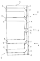
도 1은 마스터 레이저, 외부 광학면 상에 반사방지 코팅을 갖는 2개의 선형 증폭기, 및 4개의 수직 증폭기를 구비한 제안된 DSMCLE의 평면도의 개략적인 도면이다.
도 2는 마스터 레이저와 일체로 접속된 마스터 레이저와 선형 증폭기의 광축에 따른 제안된 DSMCLE의 종단면의 개략적인 도면이다.
도 3은 2개의 선형 증폭기 각각의 활성 증폭 영역이 스트라이프 부분으로 매끄럽게 연장되는 확대 부분으로 구성되고, 게다가 선형 증폭기의 외부 광학면 상에 반사방지 코팅이 없다는 점에서 도 1에 개략적으로 나타낸 DSMCLE과 다른 제안된 DSMCLE의 평면도의 개략적인 도면이다.
도 4는 대응하는 회전 요소를 통해 회전 요소 4개의 수직 증폭기가 2개의 선형 증폭기의 활성 증폭 영역에 접속되고, 그 증폭된 레이저 방출이 대향 방향으로 교대로 전파된다는 점에서 도 3에 개략적으로 나타낸 DSMCLE과 다른 제안된 DSMCLE의 평면도의 개략적인 도면이다.
도 5는 광 공진기의 비투과 반사기의 일측 상의 마스터 다이오드 레이저에 일체로 접속된다는 점에서 도 3에 개략적으로 나타낸 DSMCLE과 다른 제안된 DSMCLE의 평면도의 개략적인 도면이다.
도 6은 4개의 수직 증폭기 각각에서 종방향 광축을 따라 증폭된 레이저 방출에 대한 3개의 출력 요소가 형성된다는 점에서 도 3에 개략적으로 나타낸 DSMCLE와 다른 제안된 DSMCLE-VE의 평면도의 개략적인 도면이다.
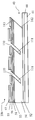
도 7은 제안된 DSMCLE-VE의 4개의 수직 증폭기 중 1개의 수직 증폭기의 종방향 부분의 개략적인 도면이며, 출력 요소는 기판을 통해 증폭된 레이저 방출의 빔의 출력을 실현한다.
도 8은 출력 요소가 헤테로 구조의 외면의 방향으로 증폭된 레이저 방출의 빔의 출력을 실현한다는 점에서 다른 도 7에 개략적으로 나타낸 수직 증폭기의 종방향 부분의 개략적인 도면이다.The invention will be described in detail below in connection with FIGS. 1, ..., and 8.
1 is a schematic diagram of a top view of a proposed DSMCLE with a master laser, two linear amplifiers with an antireflective coating on the external optical surface, and four vertical amplifiers.
2 is a schematic diagram of the longitudinal section of the proposed DSMCLE along the optical axis of the master laser and the linear amplifier connected integrally with the master laser.
FIG. 3 differs from the DSMCLE schematically shown in FIG. 1 in that the active amplification region of each of the two linear amplifiers consists of an enlarged portion that smoothly extends into the stripe portion, and furthermore there is no antireflective coating on the external optical surface of the linear amplifier. A schematic diagram of a plan view of the proposed DSMCLE.
FIG. 4 shows the DSMCLE shown schematically in FIG. 3 in that the vertical amplifiers of the four rotating elements are connected to the active amplification regions of the two linear amplifiers through corresponding rotating elements, and their amplified laser emissions propagate alternately in opposite directions. Is a schematic drawing of a plan view of the proposed DSMCLE with another.
FIG. 5 is a schematic diagram of a plan view of the proposed DSMCLE different from the DSMCLE shown schematically in FIG. 3 in that it is integrally connected to the master diode laser on one side of the non-transmissive reflector of the optical resonator.
FIG. 6 is a schematic diagram of a top view of the proposed DSMCLE-VE and other DSMCLEs schematically shown in FIG. 3 in that three output elements for amplified laser emission along the longitudinal optical axis are formed in each of the four vertical amplifiers. .
Figure 7 is a schematic drawing of the longitudinal part of one of the four vertical amplifiers of the proposed DSMCLE-VE, the output element realizing the output of the beam of laser emission amplified through the substrate.
FIG. 8 is a schematic illustration of the longitudinal portion of the vertical amplifier shown schematically in FIG. 7 in that the output element realizes the output of the beam of laser emission amplified in the direction of the outer surface of the heterostructure.
이하 본 발명은 첨부 도면을 참조하여 구체적인 실시예의 기재에 의해 설명된다. 다중빔 코히어런트 레이저 방출(DSMCLE)의 다이오드 소스 및 수직 방출 출력을 갖는 다중빔 코히어런트 레이저 방출의 다이오드 소스(DSMCLE-VE)의 실시예의 소정 예는 유일한 예가 아니고 다른 실현의 유용성(알려진 파장 범위를 포함하는)을 가정하며, 그 특징은 청구항에 따른 특징의 총합에 반영된다.The invention is illustrated by the following description of specific embodiments with reference to the accompanying drawings. Certain examples of embodiments of a diode source of multibeam coherent laser emission (DSMCLE) and a diode source of multibeam coherent laser emission (DSMCLE-VE) having a vertical emission output are not the only examples and are useful in other implementations (known wavelengths). The scope of the invention) is reflected in the sum of the features according to the claims.
고려를 위해 제안되며 도 1 - 8에 나타낸 DSMCLE 설계에서는, 이하의 기호 표시가 주어진다:In the DSMCLE design proposed for consideration and shown in Figures 1-8, the following symbolic representations are given:
10 - 제안된 DSMCLE.10-Proposed DSMCLE.
20 - 마스터 다이오드 레이저. 그 구성요소:20-master diode laser. Its components:
21 - 이하 비투과 광 반사기로 지칭되는 광 공진기의 비투과 반사기,21-non-transmissive reflectors of optical resonators, hereinafter referred to as non-transmissive light reflectors,
22 - 광 공진기의 광학면,22-optical surface of the optical resonator,
23 - 스트라이프 활성 레이징 영역.23-Stripe active lasing area.
30 - 선형 증폭기. 그 구성요소:30-linear amplifier. Its components:
31 - 스트라이프 활성 증폭 영역,31-stripe active amplification region,
32 - 외부 광학면,32-external optical plane,
33 - 반사방지 코팅,33-antireflective coating,
34 - 스트라이프 영역에 매끄러운 전이를 갖는 확대.34-magnification with smooth transition in the stripe area.
40 - 수직 증폭기. 그 구성요소:40-vertical amplifier. Its components:
41 - 확대 활성 증폭 영역,41-enlarged active amplification region,
42 - 출력 광학면,42-output optical plane,
43 - 반사방지 코팅,43-antireflective coating,
44 - 스트라이프 활성 증폭 영역.44-Stripe active amplification region.
50 - 헤테로 구조. 그 구성요소:50-heterostructure. Its components:
51 - 활성층,51-active layer,
52 - 기판 측 상의 클래딩층,52-cladding layer on the substrate side,
53 - 기판 측 상의 조정층,53-adjusting layer on the substrate side,
55 - 외층 측 상의 클래딩층,55-cladding layer on the outer layer side,
56 - 외층 측 상의 누출 영역,56-leak area on the outer layer side,
57 - p형의 외부 접촉층,57-p-type outer contact layer,
60 - 헤테로 구조를 위한 기판,60-substrate for heterostructures,
61 - 기판의 외면.61-the outer surface of the substrate.
70 - 회전 요소. 그 구성요소:70-rotating element. Its components:
71 - 광반사면,71-light reflecting surface,
72 - 클래딩층(52)에 침투되는 광반사면.72-light reflecting surface penetrating the
80 - 측면 한정 영역 for 마스터 레이저, 선형 및 수직 증폭기.80-side confinement area for master laser, linear and vertical amplifiers.
100 - DSMCLE-VE 실시예.100—DSMCLE-VE Example.
110 - 출력 요소,110-output element,
111 - 광반사면,111-light reflecting surface,
112 - 클래딩층(52)에 침투되는 광반사면,112-a light reflecting surface penetrating the
113 - 출력 방출을 위한 반사방지 코팅.113-antireflective coating for discharge of power.
제안된 DSMCLE(10)(도 1-2 참조)는 기본 모드에서 레이징되며 양단측 상의 마스터 레이저(20)에 접속된 2개의 선형 증폭기(30)와 일체로 접속되는 단일 모드 마스터 레이저(20)를 포함한다. 레이저 광 공진기의 단부에서는 비투과 광 반사기(21)가 위치된다. 외부 광학면(32) 상에 반사방지 코팅(33)을 갖는 선형 증폭기(30)는 회전 요소(70)와 확대 활성 증폭 영역(41)을 갖는 수직 증폭기(40)를 사용하여 차례로 일체 접속된다. 증폭된 레이저 방출의 출력은 4개의 수직 증폭기(40) 각각의 반사방지 광학면(42)을 통해 수행된다.The proposed DSMCLE 10 (see Figs. 1-2) is a single
DSMCLE(10)는 마스터 레이저(20) 및 상기 다이오드 증폭기(30 및 40) 둘 다에 대한 공통 레이저 헤테로 구조(50)를 기초로 하여 이루어진다. 헤테로 구조(50)는 n형 GaAs의 기판(60) 상에 성장된다. 수직 증폭기(40)와 선형 증폭기(30)의 일체형 접속은 회전 요소(70)를 사용하여 실현된다. 헤테로 구조(50)는 InAlGaAs의 1개의 활성층(51)과 AlGaAs 반도체 화합물을 기초로 하여 성장된다. 활성층(51)의 조성 및 두께에 의해 결정되는 레이저 파장은 0.976㎛와 같게 선택된다.The
기판(60) 측 상의 활성층(51)과 클래딩층(52) 사이에 제 1 누출 영역(조정층(53) 및 누출층(54)을 포함하는)이 위치된다. 활성층(51)과 클래딩층(55) 사이의 대향 측 상에는 p형의 반도체 접촉층(57)이 인접하는 제 2 누출 영역(56)(조정층 및 누출층을 포함하는)이 위치된다. 금속화층 및 대응하는 절연 유전층은 도면에 도시되어 있지 않다. 실제로, 클래딩층(52 및 55) 사이에 위치되는 헤테로 구조(50)의 모든 층 세트는 확장된 도파로 영역을 형성한다. 누출층은 AlGaAs로 이루어진다. 기판(60) 측 상의 누출층(54)의 두께는 대향 측의 누출층의 두께보다 더 큰 자릿수인 6㎛와 같게 선택된다. 0.3kA/cm2 및 5.0kA/cm2 의 현재 밀도에서 헤테로 구조(50)의 유효 굴절률(neff) 대 누출층(54)의 굴절률(nIN)의 계산된 비(neff/nIN)의 값은 각각 0.999868 및 0.999772와 같다.Between the
상술한 헤테로 구조(50)에 기초하여, 일체로 접속된 1개의 마스터 레이저(20), 2개의 선형 증폭기(30), 및 4개의 수직 증폭기(40)가 형성된다. 다이오드 레이저(20)의 광 공진기의 광학면(22) 상의 양측에는 1에 가까운 반사 계수를 갖는 반사기(21)(비투과 광 반사기)가 형성된다(코팅의 증착의 의해). 선형 증폭기(30)와 마스터 레이저(20)의 일체형 접속은 광 공진기의 비투과 반사기(21)를 바이패스시킴으로써 딥 라잉 누출층(54)을 통해 주로 실현된다. 마스터 레이저(20)의 활성 레이징 영역(23)은 9㎛의 스트라이프 폭을 갖는 스트라이프 영역으로 이루어지며, 광 공진기의 길이는 1000㎛와 같게 선택된다. 2개의 선형 증폭기(30) 각각에서의 스트라이프 활성 증폭 영역(31)의 폭 및 길이는 각각 12㎛ 및 2000㎛이다. 각 선형 증폭기(30)의 외부 광학면(32) 상에 0에 가까운(0.0001보다 더 작은) 반사 계수를 갖는 반사방지 코팅(33)이 증착된다.Based on the
각 선형 증폭기(30)와 2개의 수직 증폭기(40) 사이의 일체형 광 접속은 활성 증폭 영역(31)에서 2개의 회전 요소(70)의 배치에 의해 실현된다. 에칭에 의해 이루어진 각 회전 요소(70)는 헤테로 구조(50)의 층의 면에 직각으로 위치되고 접촉층(57)에서 누출층(54)의 두께 60%까지 내측에 수직으로 침투하는 광반사면(71)을 포함한다. 이 경우에 회전 요소(70)의 상기 반사면(71)은 선형 증폭기(30) 및 2개의 수직 증폭기(40) 둘 다에서 증폭된 방출의 전파에 대한 광축에 관하여 45°의 각도(모듈러스)로 회전된다. 각 수직 증폭기(40)의 활성 증폭 영역(41)은 6°의 확대각으로 확대되어 이루어진다. 5000㎛의 수직 증폭기의 길이에서 증폭된 방출을 출력하는 광학면(42)의 폭은 250㎛이다. 각 선형 증폭기(40) 의 출력 광학면(42) 상에 0에 가까운(0.0001보다 더 작은) 반사 계수를 갖는 반사방지 코팅(43)이 증착된다.An integral optical connection between each
동일한 주요 특성을 갖는 측면 한정 영역(80)은 2개의 선형 증폭기(30)의 각 스트라이프 활성 영역(31)뿐만 아니라 마스터 레이저(20)의 스트라이프 활성 레이징 영역(23) 및 4개의 수직 증폭기(40)의 각 확대 활성 영역(41)에 대해서도 양 측면에 인접하여 이루어진다. 상기 영역(80)은 2개의 서브영역(도면에 도시되지 않음)을 포함한다. 상기 영역(23, 31, 및 41)과 연속하는 제 1 스트라이프 분할 한정 서브영역은 헤테로 구조(50)의 활성층(51)의 라잉의 깊이에 도달하지 않는 깊이 0.7㎛에 대해 폭 2.0㎛의 홈으로서 에칭에 의해 형성된다. 상기 제 1 서브영역과 연속하는 제 2 한정 서브영역은 활성층(51)의 라잉의 면을 가로지르고 누출층(54) 두께의 60%까지 침투하는 오목 홈으로서 에칭에 의해 형성된다. 양 홈은 유전체로 충전된다.The side confined
DSMCLE(10)(도면에 도시되지 않은)의 이하의 실시예는 이 실시예에서 광 공진기의 비투과 반사기(21)가 마스터 레이저의 안정한 단일 주파수 레이징을 제공하는 분포 브래그 반사기로 형성된다는 점에서 도 1-2에 나타낸 실시예와 다르다.The following embodiment of the DSMCLE 10 (not shown in the drawings) is also shown in this embodiment in that the
DSMCLE(10)(도면에 도시되지 않은)의 이하의 실시예는 이 실시예에서 공통 헤테로 구조(50)가 그 사이에 터널 전이를 갖는 p형 및 n형의 얇게 고농도로 도핑된 층에 의해 서로 전기적으로 접속된 적어도 2개의 활성층을 포함한다는 점에서 도 1-도 2에 나타낸 실시예와 다르다.The following embodiments of DSMCLE 10 (not shown in the figures) are mutually separated by p- and n-type thinly doped layers of
DSMCLE(10)(도면에 도시되지 않은)의 이하의 실시예는 이 실시예가 20,000㎛의 각 선형 증폭기(30)의 길이에 50개의 수직 증폭기(40) 및 50개의 회전 요소(70)를 포함한다는 점에서 도 1-도 2에 나타낸 실시예와 다르다.The following embodiment of the DSMCLE 10 (not shown) shows that this embodiment includes 50
DSMCLE(10)(도 3 참조)의 이하의 실시예는 이 실시예에서 마스터 레이저에 가장 가까운 각(2개의) 활성 증폭 영역(34)이 50㎛의 스트라이프 폭을 갖는 스트라이프 부분(31)에 매끄러운 전이를 갖는 초기 부분에서 확대되어 이루어진다는 점에서 도 1-도 2에 나타낸 실시예와 다르다. 수직 증폭기(40)의 각 활성 증폭 영역(44)은 스트라이프 영역으로 이루어진다. 게다가, 마스터 레이저(20)의 광학면(22)으로부터 대부분 이동된 각 회전 요소(70)에서 광반사면(72)은 누출층(54) 두께의 100%까지 침투한다. 이 경우에 선형 증폭기(30)를 위한 반사방지 코팅(33)을 제조할 필요가 더 이상 없다. 도 3 및 도 4-6에는 측면 한정 영역이 도시되지 않은 것을 주목하자.The following embodiment of the DSMCLE 10 (see FIG. 3) shows that the angle (two)
DSMCLE(10)(도면에 도시되지 않은)의 이하의 실시예는 이 실시예에서 선형 증폭기(30)의 확대 활성 증폭 영역(34)에 인접한 측면 한정 영역(80)이 분할 한정 서브영역으로만 구성된다는 점에서 이전 실시예와 다르다.The following embodiment of the DSMCLE 10 (not shown) shows that the
DSMCLE(10)(도면에 도시되지 않은)의 이하의 실시예는 이 실시예에서 수직 증폭기(40)의 확대 활성 증폭 영역(41)에 인접한 측면 한정 영역(80)이 분할 한정 서브영역으로만 구성된다는 점에서 이전 실시예와 다르다.The following embodiment of the DSMCLE 10 (not shown) shows that the
DSMCLE(10)(도 4 참조)의 이하의 실시예는 이 실시예에 있어서 각 선형 증폭기(30)의 활성 증폭 영역(31)에서 광반사면(72)이 회전 요소(70)의 광반사면(71)에 대하여 직각(90°)으로 회전된다는 점에서 도 3에 나타낸 실시예와 다르다. 이 경우에 회전 요소(70)의 상기 광반사면(71 및 72)을 갖는 선형 증폭기(30)에 접속된 수직 증폭기(40)에서 출력 증폭된 레이저 방출이 대향 방향으로 전파된다.The following embodiment of the DSMCLE 10 (see FIG. 4) shows that in this embodiment the
DSMCLE(10)(도 5 참조)의 이하의 실시예는 이 실시예에서 마스터 레이저(20)와 선형 증폭기(30)의 일체형 접속이 광 공진기의 비투과 반사기(21)를 통해 일측 상에 수행된다는 점에서 도 3에 나타낸 실시예와 다르다. 광 공진기의 대향측에 대하여 비투과 반사기(21)가 절개된 광학면(22) 상에 형성된다. 4개의 수직 증폭기(40)의 활성 증폭 영역(41)은 4개의 회전 요소(70)를 통해 선형 증폭기(30)의 1개의 활성 증폭 영역(34) 및 3개의 스트라이프 활성 증폭 영역(31)에 접합된다.The following embodiment of the DSMCLE 10 (see FIG. 5) is that in this embodiment an integral connection of the
DSMCLE(10)의 이하의 실시예는 이 실시예에서 마스터 레이저(20), 선형 증폭기(30), 및 수직 증폭기(40)에 옴 금속화층(도면에 도시되지 않은) 사이의 얇은 분할 스트라이프의 도입에 의해 실현되는 독립적인(개별적인) 옴 접촉부가 형성된다는 점에서 이전 실시예와 다르다.The following embodiment of
이하의 도면에 나타낸 제안된 DSMCLE-VE(100)는 수직 증폭기(40)에서 활성 증폭 영역(41)을 따라 2개 이상의 일체형 출력 요소(110)가 에칭에 의해 추가적으로 형성된다는 점에서 상술한 DSMCLE 실시예와 다르다. 상기 요소(110)는 회전 요소(70)로부터 그리고 그 사이에 일정한 거리로 형성된다. 상기 요소(110)는 헤테로 구조의 층의 면에 대하여 수직 방향으로 증폭된 레이저 방출을 출력하도록 설계되어 있다.The proposed DSMCLE-
DSMCLE-VE(100)(도 6 - 7 참조)의 이하의 실시예는 이 실시예에서 에칭에 의해 형성된 각각의 일체형 출력 요소(110)가 스트라이프 활성 증폭 영역(44)에 걸쳐 위치되는 증폭된 레이저 방출을 위한 광반사면(111)을 포함한다는 점에서 이전 실시예와 다르다. 상기 면(111)은 누출층(54) 두께의 65%까지 - 45°의 경사각으로 헤테로 구조(50)(활성층(51)을 포함하는)의 층의 면을 가로지른 채로 침투된다. 회전 요소(70)로부터 대부분 이동된 출력 요소(110)를 위해 광반사면(112)은 누출층(54) 두께의 100%까지 침투한다. 기판(60)의 외측(61) 상의 증폭된 레이저 방출의 출력의 위치에서 0.0001보다 더 작은 반사 계수를 갖는 반사방지 코팅(113)이 형성된다. 기판(60)의 자유면 상의 금속화층 및 반사방지 코팅(113)은 도 7에 도시되어 있지 않다.The following embodiments of the DSMCLE-VE 100 (see FIGS. 6-7) show that in this embodiment each amplified
DSMCLE-VE(100)(도 6 및 도 8 참조)의 이하의 실시예는 이 실시예에서 일체형 출력 요소(110)의 광반사면(111)의 경사각이 + 45°인 점에서 이전 실시예와 다르다. 이 실시예에서 증폭된 레이저 방출의 출력은 기판(60)의 위치에 대향하는 방향으로 헤테로 구조(50)의 층의 면에 대한 직각에서 실현된다. 이 경우에 증폭된 레이저 방출의 출력의 장소에서 고농도로 도핑된 접촉층(57) 및 클래딩층(55)의 제거 후 0.0001보다 더 작은 반사 계수를 갖는 반사방지 코팅(113)이 증착된다. 접촉층(57)의 표면 상의 금속화층은 도 8에 도시되어 있지 않다.The following embodiments of the DSMCLE-VE 100 (see FIGS. 6 and 8) differ from the previous embodiment in that the tilt angle of the
제안된 다중빔 코히어런트 레이저 방출의 다이오드 소스, 즉 DSMCLE 및 DSMCLE-VE는 장치에서의 방출의 전파에 대한 수평면 및 헤테로 구조의 활성에 수직인 면 둘 다에서 코히어런트 레이저 방출의 매우 높은 전력과 출력 방출의 매우 낮은 발산을 생성하게 하는 것을 가능하게 한다.The diode sources of the proposed multibeam coherent laser emission, ie DSMCLE and DSMCLE-VE, have very high power of coherent laser emission in both the horizontal plane for propagation of the emission in the device and the plane perpendicular to the activity of the heterostructure. It makes it possible to produce very low divergence of over power output.
산업상 이용가능성Industrial availability
다중빔 코히어런트 레이저 방출의 다이오드 소스는 주파수 이중 레이저를 실현하기 위해, 그리고 섬유 및 고체 레이저와 광 증폭기를 펌핑하기 위해 정밀 레이저 재료 처리(레이저 커팅, 용접, 드릴링, 표면 용융, 각종 부품의 치수 처리, 레이저 마킹 및 조각), 수술과 파워 요법을 위한 레이저 장치, 레이저 거리계, 레이저 목표 지시기에 사용된다.Diode sources with multibeam coherent laser emission are used for precision laser material processing (laser cutting, welding, drilling, surface melting, dimensions of various components) to realize frequency double lasers and to pump fiber and solid state lasers and optical amplifiers. Processing, laser marking and engraving), laser devices for surgery and power therapy, laser rangefinders, laser target indicators.
Claims (21)
Applications Claiming Priority (2)
| Application Number | Priority Date | Filing Date | Title |
|---|---|---|---|
| RU2009127486/28A RU2419934C2 (en) | 2009-07-17 | 2009-07-17 | Diode multi-beam source of coherent laser radiation (versions) |
| RU2009127486 | 2009-07-17 |
Publications (1)
| Publication Number | Publication Date |
|---|---|
| KR20120034099A true KR20120034099A (en) | 2012-04-09 |
Family
ID=43449568
Family Applications (1)
| Application Number | Title | Priority Date | Filing Date |
|---|---|---|---|
| KR1020127000776A KR20120034099A (en) | 2009-07-17 | 2010-07-07 | Multibeam coherent laser diode source(embodiments) |
Country Status (10)
| Country | Link |
|---|---|
| US (1) | US8401046B2 (en) |
| EP (1) | EP2466704A1 (en) |
| JP (1) | JP2012533878A (en) |
| KR (1) | KR20120034099A (en) |
| CN (1) | CN102474074B (en) |
| CA (1) | CA2768469A1 (en) |
| IL (1) | IL217391A0 (en) |
| RU (1) | RU2419934C2 (en) |
| SG (1) | SG177488A1 (en) |
| WO (1) | WO2011008127A1 (en) |
Families Citing this family (4)
| Publication number | Priority date | Publication date | Assignee | Title |
|---|---|---|---|---|
| US10203399B2 (en) | 2013-11-12 | 2019-02-12 | Big Sky Financial Corporation | Methods and apparatus for array based LiDAR systems with reduced interference |
| US9360554B2 (en) | 2014-04-11 | 2016-06-07 | Facet Technology Corp. | Methods and apparatus for object detection and identification in a multiple detector lidar array |
| US10036801B2 (en) | 2015-03-05 | 2018-07-31 | Big Sky Financial Corporation | Methods and apparatus for increased precision and improved range in a multiple detector LiDAR array |
| US9866816B2 (en) | 2016-03-03 | 2018-01-09 | 4D Intellectual Properties, Llc | Methods and apparatus for an active pulsed 4D camera for image acquisition and analysis |
Family Cites Families (7)
| Publication number | Priority date | Publication date | Assignee | Title |
|---|---|---|---|---|
| US4063189A (en) | 1976-04-08 | 1977-12-13 | Xerox Corporation | Leaky wave diode laser |
| RU2134007C1 (en) * | 1998-03-12 | 1999-07-27 | Государственное предприятие Научно-исследовательский институт "Полюс" | Semiconductor optical amplifier |
| RU2142665C1 (en) * | 1998-08-10 | 1999-12-10 | Швейкин Василий Иванович | Injection laser |
| JP2003078209A (en) * | 2001-09-05 | 2003-03-14 | Fujitsu Ltd | Optical semiconductor device |
| RU2197048C1 (en) | 2002-02-18 | 2003-01-20 | Швейкин Василий Иванович | Injection laser |
| RU2278455C1 (en) | 2004-11-17 | 2006-06-20 | Василий Иванович Швейкин | Hetero-structure, injection laser, semiconductor amplifying element and semiconductor optical amplifier |
| DE102006061532A1 (en) * | 2006-09-28 | 2008-04-03 | Osram Opto Semiconductors Gmbh | Edge-emitting semiconductor laser with a plurality of monolithically integrated laser diodes |
-
2009
- 2009-07-17 RU RU2009127486/28A patent/RU2419934C2/en not_active IP Right Cessation
-
2010
- 2010-07-07 WO PCT/RU2010/000377 patent/WO2011008127A1/en active Application Filing
- 2010-07-07 CA CA2768469A patent/CA2768469A1/en not_active Abandoned
- 2010-07-07 JP JP2012520561A patent/JP2012533878A/en not_active Withdrawn
- 2010-07-07 SG SG2012000279A patent/SG177488A1/en unknown
- 2010-07-07 KR KR1020127000776A patent/KR20120034099A/en not_active Application Discontinuation
- 2010-07-07 US US13/384,531 patent/US8401046B2/en not_active Expired - Fee Related
- 2010-07-07 EP EP10800095A patent/EP2466704A1/en not_active Withdrawn
- 2010-07-07 CN CN201080032186.9A patent/CN102474074B/en not_active Expired - Fee Related
-
2012
- 2012-01-05 IL IL217391A patent/IL217391A0/en unknown
Also Published As
| Publication number | Publication date |
|---|---|
| RU2009127486A (en) | 2011-01-27 |
| CA2768469A1 (en) | 2011-01-20 |
| US8401046B2 (en) | 2013-03-19 |
| IL217391A0 (en) | 2012-02-29 |
| JP2012533878A (en) | 2012-12-27 |
| SG177488A1 (en) | 2012-02-28 |
| US20120113998A1 (en) | 2012-05-10 |
| EP2466704A1 (en) | 2012-06-20 |
| CN102474074A (en) | 2012-05-23 |
| WO2011008127A1 (en) | 2011-01-20 |
| RU2419934C2 (en) | 2011-05-27 |
| CN102474074B (en) | 2014-01-01 |
Similar Documents
| Publication | Publication Date | Title |
|---|---|---|
| JP4621393B2 (en) | Surface emitting semiconductor laser and method for manufacturing surface emitting semiconductor laser | |
| WO1997047042A9 (en) | Light emitting semiconductor device | |
| EP0902978A1 (en) | Light emitting semiconductor device | |
| US6744804B2 (en) | Edge emitting lasers using photonic crystals | |
| RU2391756C2 (en) | Diode laser, integrated diode laser and integrated semiconductor optical amplifier | |
| KR100860696B1 (en) | Vertical cavity surface emitting laser | |
| JP2014078567A (en) | Semiconductor laser device | |
| KR20120034099A (en) | Multibeam coherent laser diode source(embodiments) | |
| US20100135348A1 (en) | Method for improvement of beam quality and wavelength stabilized operation of a semiconductor diode laser with an extended waveguide | |
| JP2005039102A (en) | Surface emitting laser | |
| KR101112682B1 (en) | Injection laser | |
| WO2008103679A2 (en) | Vertically emitting laser and method of making the same | |
| JP2004266280A (en) | Semiconductor laser and optically-pumped semiconductor device | |
| JPS63150981A (en) | Semiconductor laser | |
| RU2230410C1 (en) | Injection laser and laser diode strip | |
| RU2398325C2 (en) | Diode multi-beam source of coherent laser radiation | |
| RU2047935C1 (en) | Optically pumped semiconductor laser | |
| JPH01238082A (en) | Semiconductor laser | |
| TW201230566A (en) | Diode source of multibeam coherent laser emission | |
| JPH0430490A (en) | Manufacture of semiconductor laser element | |
| JP2005026611A (en) | Semiconductor laser element | |
| JP2010129955A (en) | Distributed feedback semiconductor laser |
Legal Events
| Date | Code | Title | Description |
|---|---|---|---|
| WITN | Application deemed withdrawn, e.g. because no request for examination was filed or no examination fee was paid |