KR20120006502A - Resistive-switching memory elements having improved switching characteristics - Google Patents
Resistive-switching memory elements having improved switching characteristics Download PDFInfo
- Publication number
- KR20120006502A KR20120006502A KR1020117023491A KR20117023491A KR20120006502A KR 20120006502 A KR20120006502 A KR 20120006502A KR 1020117023491 A KR1020117023491 A KR 1020117023491A KR 20117023491 A KR20117023491 A KR 20117023491A KR 20120006502 A KR20120006502 A KR 20120006502A
- Authority
- KR
- South Korea
- Prior art keywords
- layer
- electrode
- oxide
- change
- metal
- Prior art date
Links
Images


Classifications
-
- H—ELECTRICITY
- H10—SEMICONDUCTOR DEVICES; ELECTRIC SOLID-STATE DEVICES NOT OTHERWISE PROVIDED FOR
- H10N—ELECTRIC SOLID-STATE DEVICES NOT OTHERWISE PROVIDED FOR
- H10N70/00—Solid-state devices without a potential-jump barrier or surface barrier, and specially adapted for rectifying, amplifying, oscillating or switching
- H10N70/20—Multistable switching devices, e.g. memristors
- H10N70/25—Multistable switching devices, e.g. memristors based on bulk electronic defects, e.g. trapping of electrons
-
- H—ELECTRICITY
- H10—SEMICONDUCTOR DEVICES; ELECTRIC SOLID-STATE DEVICES NOT OTHERWISE PROVIDED FOR
- H10N—ELECTRIC SOLID-STATE DEVICES NOT OTHERWISE PROVIDED FOR
- H10N70/00—Solid-state devices without a potential-jump barrier or surface barrier, and specially adapted for rectifying, amplifying, oscillating or switching
- H10N70/20—Multistable switching devices, e.g. memristors
- H10N70/24—Multistable switching devices, e.g. memristors based on migration or redistribution of ionic species, e.g. anions, vacancies
-
- H—ELECTRICITY
- H10—SEMICONDUCTOR DEVICES; ELECTRIC SOLID-STATE DEVICES NOT OTHERWISE PROVIDED FOR
- H10B—ELECTRONIC MEMORY DEVICES
- H10B63/00—Resistance change memory devices, e.g. resistive RAM [ReRAM] devices
- H10B63/20—Resistance change memory devices, e.g. resistive RAM [ReRAM] devices comprising selection components having two electrodes, e.g. diodes
-
- H—ELECTRICITY
- H10—SEMICONDUCTOR DEVICES; ELECTRIC SOLID-STATE DEVICES NOT OTHERWISE PROVIDED FOR
- H10B—ELECTRONIC MEMORY DEVICES
- H10B63/00—Resistance change memory devices, e.g. resistive RAM [ReRAM] devices
- H10B63/80—Arrangements comprising multiple bistable or multi-stable switching components of the same type on a plane parallel to the substrate, e.g. cross-point arrays
- H10B63/84—Arrangements comprising multiple bistable or multi-stable switching components of the same type on a plane parallel to the substrate, e.g. cross-point arrays arranged in a direction perpendicular to the substrate, e.g. 3D cell arrays
-
- H—ELECTRICITY
- H10—SEMICONDUCTOR DEVICES; ELECTRIC SOLID-STATE DEVICES NOT OTHERWISE PROVIDED FOR
- H10N—ELECTRIC SOLID-STATE DEVICES NOT OTHERWISE PROVIDED FOR
- H10N70/00—Solid-state devices without a potential-jump barrier or surface barrier, and specially adapted for rectifying, amplifying, oscillating or switching
- H10N70/011—Manufacture or treatment of multistable switching devices
- H10N70/021—Formation of the switching material, e.g. layer deposition
- H10N70/023—Formation of the switching material, e.g. layer deposition by chemical vapor deposition, e.g. MOCVD, ALD
-
- H—ELECTRICITY
- H10—SEMICONDUCTOR DEVICES; ELECTRIC SOLID-STATE DEVICES NOT OTHERWISE PROVIDED FOR
- H10N—ELECTRIC SOLID-STATE DEVICES NOT OTHERWISE PROVIDED FOR
- H10N70/00—Solid-state devices without a potential-jump barrier or surface barrier, and specially adapted for rectifying, amplifying, oscillating or switching
- H10N70/011—Manufacture or treatment of multistable switching devices
- H10N70/041—Modification of the switching material, e.g. post-treatment, doping
-
- H—ELECTRICITY
- H10—SEMICONDUCTOR DEVICES; ELECTRIC SOLID-STATE DEVICES NOT OTHERWISE PROVIDED FOR
- H10N—ELECTRIC SOLID-STATE DEVICES NOT OTHERWISE PROVIDED FOR
- H10N70/00—Solid-state devices without a potential-jump barrier or surface barrier, and specially adapted for rectifying, amplifying, oscillating or switching
- H10N70/20—Multistable switching devices, e.g. memristors
-
- H—ELECTRICITY
- H10—SEMICONDUCTOR DEVICES; ELECTRIC SOLID-STATE DEVICES NOT OTHERWISE PROVIDED FOR
- H10N—ELECTRIC SOLID-STATE DEVICES NOT OTHERWISE PROVIDED FOR
- H10N70/00—Solid-state devices without a potential-jump barrier or surface barrier, and specially adapted for rectifying, amplifying, oscillating or switching
- H10N70/801—Constructional details of multistable switching devices
- H10N70/821—Device geometry
- H10N70/826—Device geometry adapted for essentially vertical current flow, e.g. sandwich or pillar type devices
-
- H—ELECTRICITY
- H10—SEMICONDUCTOR DEVICES; ELECTRIC SOLID-STATE DEVICES NOT OTHERWISE PROVIDED FOR
- H10N—ELECTRIC SOLID-STATE DEVICES NOT OTHERWISE PROVIDED FOR
- H10N70/00—Solid-state devices without a potential-jump barrier or surface barrier, and specially adapted for rectifying, amplifying, oscillating or switching
- H10N70/801—Constructional details of multistable switching devices
- H10N70/881—Switching materials
- H10N70/883—Oxides or nitrides
- H10N70/8833—Binary metal oxides, e.g. TaOx
Abstract
개선된 변화 특징들을 갖는 저항-변화 메모리 소자들이 제공되고, 이 소자들은 제 1 전극 및 제 2 전극, 상기 제 1 전극과 제 2 전극 사이에 있고 4 전자 볼트(eV)보다 큰 제 1 밴드갭을 갖는 제 1 금속 산화물을 포함하며 제 1 두께를 갖는 변화 층, 및 상기 변화 층과 제 2 전극 사이에 있고 상기 제 1 밴드갭보다 큰 제 2 밴드갭을 갖는 제 2 금속 산화물을 포함하며 상기 제 1 두께보다 25% 작은 제 2 두께를 갖는 커플링 층을 포함한다.Resistance-changing memory devices having improved change characteristics are provided, which devices include a first bandgap between a first electrode and a second electrode, between the first and second electrodes and larger than 4 electron volts (eV). A first metal oxide having a first metal oxide having a first thickness, and a second metal oxide between the second layer and the second electrode and having a second bandgap greater than the first bandgap; A coupling layer having a second thickness of 25% less than the thickness.
Description
관련 출원의 상호 참조Cross Reference of Related Application
본 출원은 "도핑된 실리콘 전극을 포함하는 저항 변화 메모리 소자(RESISTIVE SWITCHING MEMORY ELEMENT INCLUDING DOPED SILICON ELECTRODE)"의 명칭으로 2009년 4월 10일자로 출원된 미국 가 출원 제61/168,534호, "도핑된 실리콘 전극을 포함하는 저항 변화 메모리 소자(RESISTIVE SWITCHING MEMORY ELEMENT INCLUDING DOPED SILICON ELECTRODE)"의 명칭으로 2009년 10월 29일자로 출원된 미국 실용 출원 제12/608,934호, "개선된 변화 특징들을 갖는 저항 변화 메모리 소자들(RESISTIVE SWITCHING MEMORY ELEMENTS HAVING IMPROVED SWITCHING CHARACTERISTICS)"의 명칭으로 2009년 10월 30일자로 출원된 미국 실용 출원 제12/610,236호, 및 "개선된 변화 특징들을 갖는 저항-변화 메모리 소자들(RESISTIVE-SWITCHING MEMORY ELEMENTS HAVING IMPROVED SWITCHING CHARACTERISTICS)"의 명칭으로 2010년 2월 12일자로 출원된 미국 실용 출원 제12/705,474호의 우선권을 청구하고, 이들 모두는 본원 명세서에 참조로서 합체되었다.This application is directed to US Provisional Application No. 61 / 168,534, filed Apr. 10, 2009 entitled "RESISTIVE SWITCHING MEMORY ELEMENT INCLUDING DOPED SILICON ELECTRODE", "Doped RESISTIVE SWITCHING MEMORY ELEMENT INCLUDING DOPED SILICON ELECTRODE, filed Oct. 29, 2009, entitled "RESISTIVE SWITCHING MEMORY ELEMENT INCLUDING DOPED SILICON ELECTRODE" RESITIVE SWITCHING MEMORY ELEMENTS HAVING IMPROVED SWITCHING CHARACTERISTICS. RESISTIVE-SWITCHING MEMORY ELEMENTS HAVING IMPROVED SWITCHING CHARACTERISTICS) and claims priority to US Utility Application No. 12 / 705,474, filed Feb. 12, 2010. All of which are incorporated herein by reference.
발명의 분야Field of invention
본 발명은 일반적으로 반도체 메모리들에 관한 것이다. 특히, 개선된 변화 특징들을 갖는 저항-변화 메모리 소자들(resistive-switching memory elements)이 기술된다.
The present invention relates generally to semiconductor memories. In particular, resistive-switching memory elements with improved change characteristics are described.
비-휘발성 메모리들(non-volatile memories)은 파워가 차단될 때에 메모리들의 콘텐츠(contents)를 유지하는 반도체 메모리들이다. 비-휘발성 메모리들은 일반적으로 컴퓨터 시스템들, 내장 시스템들 및 지속적 저장을 필요로 하는 다른 전자 장치들뿐만 아니라 디지털 카메라들, 휴대 전화들(cellular telephones), 및 음악 플레이어들과 같은 전자 장치들에서 저장을 위해 사용된다. 비-휘발성 반도체 메모리들은 제거가능하고 휴대가능한 메모리 카드들 또는 다른 메모리 모듈들의 형태를 취할 수 있고, 다른 형태의 회로들 또는 장치들에 통합될 수 있고, 또는 임의의 다른 원하는 형태를 취할 수 있다. 비-휘발성 반도체 메모리들은 소형 사이즈와 지속성(persistence)을 갖고, 어떤 이동 부품들을 갖지 않으며, 동작하기 위해 저전력을 요구하는 그들의 이점 때문에 더욱 널러 유포되고 있다.Non-volatile memories are semiconductor memories that retain the contents of the memories when power is interrupted. Non-volatile memories are typically stored in electronic systems such as digital cameras, cellular telephones, and music players, as well as computer systems, embedded systems, and other electronic devices that require persistent storage. Used for Non-volatile semiconductor memories may take the form of removable and portable memory cards or other memory modules, may be incorporated into other forms of circuits or devices, or may take any other desired form. Non-volatile semiconductor memories are more prevalent because of their advantages of small size and persistence, no moving parts, and low power requirements for operation.
플래시 메모리는 다양한 장치들에서 사용되는 공통 형태의 비-휘발성 메모리이다. 플래시 메모리는 긴 액세스(access), 소거(erase), 및 기입 시간(write times)으로 초래될 수 있는 아키텍처(architecture)를 사용한다. 전자 장치들의 동작 속도 및 사용자들의 저장 요구(demands)는 급속하게 증가하고 있다. 플래시 메모리는 많은 경우에, 비-휘발성 메모리 요구들에 부적절한 것으로 밝혀지고 있다. 부가적으로, 휘발성 메모리들(랜덤 액세스 메모리들(RAM))(random access memory)과 같은)은 비-휘발성 메모리들의 속도가 RAM 및 휘발성 메모리들을 현재 사용하는 다른 애플리케이션들(applications)을 위한 요구조건들을 충족시키기 위해 증가한다면 비-휘발성 메모리들로 잠재적으로 대체될 수 있다.
Flash memory is a common type of non-volatile memory used in various devices. Flash memory uses an architecture that can result in long access, erase, and write times. The speed of operation of electronic devices and the storage demands of users are increasing rapidly. Flash memory has in many cases been found to be inadequate for non-volatile memory requirements. Additionally, volatile memories (such as random access memories) are requirements for the speed of non-volatile memories for other applications currently using RAM and volatile memories. Can be potentially replaced with non-volatile memories if increased to meet the requirements.
저항-변화 메모리들은 설정(set) 전압의 적용시 제 1 저항성(resistivity)으로부터 제 2 저항성까지, 그리고 재설정(reset) 전압의 적용시 제 2 저항성으로부터 다시 제 1 저항성까지 변경하는 저항-변화 물질(예를 들어, 금속 산화물)을 포함하는 메모리들이다. 기존 저항-변화 메모리들은 일부 적용들을 위해 적합하지 않은 변화 특징들(characteristics)(예를 들어, 설정, 재설정, 및 형성 전압들(forming voltages), 유지성(retention))을 갖는다.Resistance-changing memories have a resistance-change material that changes from a first resistivity to a second resistivity upon application of a set voltage and from a second resistivity back to a first resistivity upon application of a reset voltage. For example, metal oxides). Existing resistance-change memories have change characteristics (eg, set, reset, and forming voltages, retention) that are not suitable for some applications.
따라서, 개선된 변화 특징들을 갖는 저항-변화 메모리가 필요하다.
Thus, there is a need for a resistance-change memory with improved change characteristics.
본 발명의 다양한 실시예들은 다음의 상세한 설명 및 첨부한 도면들에 개시된다.
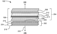
도 1은 저항-변화 메모리 소자들의 메모리 어레이(array)를 도시한 도면이다.
도 2a는 저항-변화 물질(material) 및 선택(select) 소자를 포함하는 메모리 소자를 도시한 도면이다.
도 2b는 일 실시예에 따른 메모리 소자의 일 부분의 확대도이다.
도 3 및 도 4는 계면 층(interface layer)을 갖는(도 3) 및 갖지 않는(도 4) 메모리 소자에서 에너지 레벨들을 도시한 밴드 다이아그램들이다.
도 5는 계면 층의 존재시 형성 전압의 종속관계(dependency)를 도시하는 그래프이다.
도 6은 선택 소자로서 사용되는 다이오드를 갖는 전극을 공유하는(shares) 메모리 소자를 도시한 도면이다.
도 7은 본 명세서에 기재된 메모리 소자들을 사용하는 3-차원 메모리 어레이의 일 부분을 도시한 도면이다.
도 8a 및 도 8b는 메모리 소자를 도시하고 계면 층을 사용하는 메모리 소자 내에 산소 공극들(oxygen vacancies)(결함들(defects))의 생성 및 조작(manipulation)을 도시한 도면이다.
도 9는 메모리 소자에 대한 전류(I) 대 전압(V)의 대수 관계 구상도이다.
도 10은 저항 상태 변경을 설명하는 메모리 소자에 대한 전류(I) 대 전압(V)의 대수 관계 구상도이다.
도 11 및 도 12는 본 명세서에서 설명되는 메모리 소자들에 사용되는 여러 가지 물질들(금속 산화물들)에 대한 금속 산화물 층의 두께들과 결과적인 설정 전압들(set voltages), 재설정 전압들(reset voltages), 및 온/오프 전류 비율들(on/off current ratios) 사이의 관계를 도시하는 그래프이다.
도 13 및 도 14는 계면 층들의 제어를 위한 공정들을 설명하는 흐름도이다.
도 15는 다양한 실시예들에 따른 메모리 소자를 형성하기 위한 공정을 설명하는 흐름도이다.
도 16a는 저항-변화 메모리 소자의 낮은 일 함수(work funcion) 전극이 음(nagative) 전압 설정 펄스 및 양(positive) 전압 재설정 펄스를 수신할 때에 높은 사이클링 양산율(yield)을 도시하는 그래프이다.
도 16b는 저항-변화 메모리 소자의 두 전극들이 0.1 eV 보다 높으나 1.0 eV 보다 낮은 다양한 일 함수들을 갖는 경우에 높은 사이클링 양산율을 도시하는 그래프이다.Various embodiments of the invention are disclosed in the following detailed description and the accompanying drawings.
1 illustrates a memory array of resistance-changing memory elements.
FIG. 2A illustrates a memory device including a resistance-change material and a select device.
2B is an enlarged view of a portion of a memory device according to an embodiment.
3 and 4 are band diagrams showing energy levels in a memory device with and without an interface layer (FIG. 3).
5 is a graph showing the dependency of the formation voltage in the presence of an interfacial layer.
FIG. 6 shows a memory element that shares an electrode with a diode used as the selection element.
FIG. 7 illustrates a portion of a three-dimensional memory array using the memory elements described herein.
8A and 8B illustrate the memory device and illustrate the creation and manipulation of oxygen vacancies (defects) in the memory device using an interfacial layer.
9 is a schematic diagram of the logarithmic relationship of current I versus voltage V for a memory device.
Fig. 10 is a schematic diagram of the logarithmic relationship of current (I) vs. voltage (V) for a memory element illustrating a resistance state change.
11 and 12 show the thicknesses of the metal oxide layer and the resulting set voltages and reset voltages for the various materials (metal oxides) used in the memory devices described herein. voltages) and on / off current ratios.
13 and 14 are flow charts describing processes for control of interfacial layers.
15 is a flowchart illustrating a process for forming a memory device according to various embodiments.
FIG. 16A is a graph showing high cycling yield when a low work funcion electrode of a resistance-change memory element receives a negative voltage set pulse and a positive voltage reset pulse. FIG.
FIG. 16B is a graph showing high cycling yield when two electrodes of a resistance-change memory device have various work functions higher than 0.1 eV but lower than 1.0 eV.
하나 이상의 실시예들의 상세한 설명은 첨부한 도면들에 따라 이하에서 설명된다. 상세한 설명은 그러한 실시예들과 관련하여 설명되지만, 임의의 특정 실례로 제한되지는 않는다. 범주는 청구범위에 의해서만 제한되며, 많은 대안물들, 변경물들 및 등가물들이 포함된다. 많은 특정 세부사항들은 철저한 이해를 제공하기 위해 다음의 설명에서 설명된다. 이러한 세부사항은 실례의 목적으로 제공되며, 설명된 기술은 그러한 세부사항 중 일부 또는 모두가 없이도 청구범위에 따라 구현될 수 있다. 명료성을 위해, 실시예들과 관련된 기술 분야들에 알려져 있는 기술적 물질은 설명을 불필요하게 모호하게 하는 것을 회피하기 위해 상세히 설명되지 않았다.A detailed description of one or more embodiments is described below in accordance with the accompanying drawings. The detailed description is described with reference to such embodiments, but is not limited to any particular example. The scope is limited only by the claims, and includes many alternatives, modifications and equivalents. Many specific details are set forth in the following description to provide a thorough understanding. These details are provided for the purpose of illustration and the described techniques may be implemented in accordance with the claims without some or all of those details. For clarity, technical material known in the technical fields related to the embodiments has not been described in detail in order to avoid unnecessarily obscuring the description.
다양한 실시예들에 따르면, 저항-변화 메모리 소자들(resistive-switching memory elements)이 본 명세서에 기재된다. 메모리 소자들은 일반적으로 금속-절연체-금속(metal-insulator-metal)(MIM) 구조를 갖고, 이 구조에서 적어도 하나의 절연 층(insulating layer)은 두 개의 전도성(conductive) 전극들에 의해 둘러싸인다. 본 명세서에 기재된 몇몇 실시예들은 4.0 eV보다 큰 밴드갭(bandgpap)(예를 들어, 하프늄 산화물(HfO2), 밴드갭=5.7 eV, 두께 ~ 20-100Å)을 갖는 변화 물질의 변화 층(switching layer) 및 여러 물질들, 예를 들어 ZrO2, Al2O3, TiO2, Ti/TiO2 등 중 하나 일 수 있는 커플링 층(coupling layer)을 둘러싸는 다양한 물질들의 전극들(예를 들어, 하나의 전극이 도핑된 실리콘이고 하나가 티타늄 질화물이다)을 포함하는 메모리 소자들이다. 몇몇 실시예들에서, 커플링 층은 변화 층보다 높은 밴드갭(예를 들어, 지르코늄 산화물(ZrO2), 밴드갭 = 5.8 eV; 또는 알루미늄 산화물(Al2O3), 밴드갭 = 8.4 eV)을 갖는다. 커플링 층은 변화 층의 두께보다 25퍼센트(%) 작은 두께를 갖고, 커플링 층을 포함하는 메모리 소자들은 나타난 개선된 변화 특징들(예를 들어, 보다 낮은 설정, 재설정 및 형성 전압, 및 더 양호한 유지성)을 갖는다.According to various embodiments, resistive-switching memory elements are described herein. Memory elements generally have a metal-insulator-metal (MIM) structure in which at least one insulating layer is surrounded by two conductive electrodes. Some embodiments described herein switch switching layers of change material with bandgpap greater than 4.0 eV (eg, hafnium oxide (HfO 2 ), bandgap = 5.7 eV, thickness ˜20-100 Hz). layer) and electrodes of various materials surrounding the coupling layer, which may be one of several materials, for example ZrO 2 , Al 2 O 3 , TiO 2 , Ti / TiO 2, etc. (eg , One electrode is doped silicon and one is titanium nitride). In some embodiments, the coupling layer has a higher bandgap (eg, zirconium oxide (ZrO 2 ), bandgap = 5.8 eV; or aluminum oxide (Al 2 O 3 ), bandgap = 8.4 eV) than the change layer Has The coupling layer has a thickness of 25 percent (%) less than the thickness of the change layer, and memory elements comprising the coupling layer exhibit improved change characteristics (eg, lower set-up, reset and build-up voltages, and more). Good retention).
다른 실시예들에서, 금속-리치(metal-rich) 금속 산화물 변화 층 및 금속-리치 변화 층을 형성하기 위한 기술들이 설명된다. 금속-리치 변화 층은 증가된 수의 결함들(예를 들어, 산소 공극들(oxygen vacancies))을 포함하고, 이 결함은 변화 특징들을 개선하기 위해 조정될 수 있다. 금속-리치 변화 층은 예를 들어, 원자 층 증착(atomic layer deposition: ALD) 공정 동안에 도입되는 산화제(oxidant)의 양을 감소시킴으로써 증착될 수 있다. 다른 실시예들에서, 전극과 위에 증착되는 변화 층 사이의 계면 층(interface layer)의 사이즈를 제거 또는 제어하기 위한 기술들이 설명된다.
In other embodiments, techniques for forming a metal-rich metal oxide changing layer and a metal-rich changing layer are described. The metal-rich change layer contains an increased number of defects (eg, oxygen vacancies), which defects can be adjusted to improve change characteristics. The metal-rich change layer may be deposited, for example, by reducing the amount of oxidant introduced during the atomic layer deposition (ALD) process. In other embodiments, techniques are described for removing or controlling the size of an interface layer between an electrode and a change layer deposited thereon.
I. 변화 동작(I. Change Behavior ( SwitchingSwitching OperationOperation ))
본 명세서에 기재된 메모리 소자들의 저항 변화는 메모리 소자의 금속 산화물 변화 층에서 결함들(defects)에 의해 야기되는 것으로 간주된다. 일반적으로, 결함들은 증착된 금속 산화물에 형성 또는 이미 존재하고, 존재하는 결함들은 부가적인 공정들에 의해 강화될 수 있다. 예를 들어, 물리적 기상 증착(physical vapor deposition)(PVD) 공정들 및 원자 층 증착(ALD) 공정들은 몇몇 불완전성(imperfections) 또는 흠들(flaws)을 가질 수 있는 층들을 증착한다. 결함들은 금속 산화물의 구조에서 전하(charge)로 공극들(variances)의 형태를 취할 수 있고: 몇몇 전하 캐리어들(carriers)은 구조(structure)로부터 결여될 수 있고(즉, 공극들(vacancies)), 부가적인 전하 캐리어들은 존재할 수 있거나(즉, 침입물(interstitials)), 또는 하나의 소자는 다른 것들을 위해 대체될 수 있다(즉, 대체물(substitutional)).The change in resistance of the memory devices described herein is considered to be caused by defects in the metal oxide change layer of the memory device. In general, defects are formed or already present in the deposited metal oxide, and the existing defects can be enhanced by additional processes. For example, physical vapor deposition (PVD) processes and atomic layer deposition (ALD) processes deposit layers that may have some imperfections or flaws. Defects can take the form of voids in the structure of the metal oxide as charges: some charge carriers may be missing from the structure (ie vacancies) , Additional charge carriers may be present (ie, interstitials), or one element may be replaced for others (ie, substitutional).
결함들은 금속 산화물의 벌크(bulk)에서 및/또는 금속 산화물의 계면에서 및 인접하는 층들에서 전기적으로 활성 상태인 결함들(또한 트랩들(traps)로 알려짐)로 되게 한다. 트랩들은 한 세트의 전압(고 저항성(resistivity) 상태에서 저 저항성 상태로의 변화)의 인가에 의해 충전될 수 있고, 재설정 전압(reset voltage)(저 저항성 상태에서 고 저항성 상태로의 변화)을 인가함으로써 비워진다고 간주된다. 트랩들은 증착된 금속 산화물에서 고유한 것(즉, 금속 산화물의 형성으로부터 존재하는 것)일 수 있거나 또는 도핑과 다른 공정들에 의해 생성 및/또는 증대될 수 있다. 도핑은 변화 층과 상호 확산화는(interdiffuse) 인접한 "도핑(doping) 층들을 사용, 주입(implantation)을 사용, 또는 다른 기술들을 사용하여 수행될 수 있다.Defects lead to defects (also known as traps) that are electrically active at the bulk of the metal oxide and / or at the interface of the metal oxide and in adjacent layers. The traps can be charged by the application of a set of voltages (changes from a high resistivity state to a low resistivity state) and apply a reset voltage (changes from a low resistivity state to a high resistivity state). It is considered to be emptied. The traps may be inherent in the deposited metal oxide (ie, present from the formation of the metal oxide) or may be generated and / or augmented by doping and other processes. Doping may be performed using adjacent " doping layers interdiffusing with the change layer, using implantation, or using other techniques.
변화 층에 있는 결함들은 설정 전압(set voltage)의 적용 시에 전도성 투과 경로들(percolation paths)을 형성하는 것으로 간주된다. 투과 경로들은 재설정 전압의 적용 시에 제거되는 것으로 간주된다. 예를 들면, 하프늄 산화물 층은 투과 경로들을 생성하고 하프늄 산화물 층의 전도성을 변경하기 위해 사용될 수 있는 트랩들을 형성할 수 있는 산소 또는 하프늄 공극들이나 또는 산소 또는 하프늄 침입물들을 포함할 수 있다.Defects in the change layer are considered to form conductive percolation paths upon application of a set voltage. The transmission paths are considered to be removed upon application of the reset voltage. For example, the hafnium oxide layer can include oxygen or hafnium pores or oxygen or hafnium infiltrates that can form traps that can be used to create transmission paths and change the conductivity of the hafnium oxide layer.
저항-변화 메모리 소자들의 변화 특징들은 금속 산화물들 내에서 결함들을 제어함으로써 조정될 수 있다. 변화 특징들은 동작 전압들(예를 들어, 설정, 재설정 및 형성 전압들), 동작 전류들(예를 들어, 온 및 오프 전류들), 및 데이터 유지성(retention)을 포함한다. 결함 제어는 변화 층 내에서 형태, 밀도, 에너지 레벨, 및 공간적 분포에 의해 달성된다. 그런 다음, 이들 결함들은 이들이 충전되는지(부동화된/보상된(passivated/compensated)) 또는 충전되지 않는지(보상되지 않음(uncompensated))에 기초하여 전류 흐름을 조절한다. 여러 층들을 부가하고, 변화 층의 형성을 제어하며, 주입하고, 응력을 제어하면, 임의의 열 처리들은 결함 특징들을 제어하기 위해 모두 사용된다. 부가로, 결함들은 이동될 필요가 없다. 예를 들면, 커플링 층(212)(도 2a 참조) 및 계면 층(214)(도 2a 및 도 8a 내지 도 8b 참조)은 위치들, 깊이들, 밀도들, 및/또는 결함들의 형태를 제어하기 위해 사용될 수 있고, 기술들은 증가된 수의 결함들을 갖는 변화 층을 형성하기 위해 사용될 수 있다.The changing characteristics of the resistance-changing memory elements can be adjusted by controlling the defects in the metal oxides. Change characteristics include operating voltages (eg, set, reset and shaping voltages), operating currents (eg, on and off currents), and data retention. Defect control is achieved by shape, density, energy level, and spatial distribution within the change layer. These defects then regulate the current flow based on whether they are charged (passivated / compensated) or not charged (uncompensated). By adding several layers, controlling the formation of the change layer, injecting and controlling the stress, any thermal treatments are all used to control the defect characteristics. In addition, the defects do not have to be moved. For example, coupling layer 212 (see FIG. 2A) and interfacial layer 214 (see FIGS. 2A and 8A-8B) control positions, depths, densities, and / or shapes of defects. Technology can be used to form a change layer with an increased number of defects.
부가로, 금속 산화물 변화 층은 임의의 상(phase)(예를 들어, 결정(crystalline) 및 비결정(amorphous)) 또는 복수의 상들의 혼합물을 가질 수 있다. 비결정-상 금속 산화물은 증가된 저항성을 가질 수 있고, 몇몇 실시예에서 이 저항성은 메모리 소자에 대한 잠재적인 손상을 감소시키기 위해 상기 장치의 동작 전류들을 낮출 수 있다.
In addition, the metal oxide changing layer can have any phase (eg, crystalline and amorphous) or a mixture of a plurality of phases. Amorphous-phase metal oxides may have increased resistance, and in some embodiments, this resistance may lower the operating currents of the device to reduce potential damage to the memory device.
Ⅱ. 메모리 구조(II. Memory structure ( MemoryMemory StructureStructure ))
A. 메모리 어레이(A. Memory array MemoryMemory ArrayArray ))
도 1은 저항-변화 메모리 소자들(102)의 메모리 어레이(100)를 도시한다. 메모리 어레이(100)는 메모리 디바이스 또는 다른 집적 회로의 일부일 수 있다. 메모리 어레이(100)는 잠재적 메모리 구성의 실례이며, 여러 가지 다른 구성들이 가능하다는 것이 이해된다.1 shows a
판독 및 기입 회로는 신호 라인들(104) 및 직교(orthogonal) 신호 라인들(106)을 사용하여 메모리 소자(102)에 접속될 수 있다. 신호 라인들(104) 및 신호 라인들(106)과 같은 신호 라인들은 때때로 워드 라인들(word lines) 및 비트 라인들(bit lines)이라 지칭되며, 어레이(100)의 소자들(102)에서 데이터를 판독하고 기입하는데 사용된다. 개별적인 메모리 소자들(102) 또는 메모리 소자들(102)의 그룹들은 적절한 세트의 신호 라인들(104, 106)을 이용하여 어드레스될(addressed) 수 있다. 메모리 소자(102)는 아래에서 더 상세히 설명되는 바와 같이 물질들(materials) 중 하나 이상의 층들(108)로부터 형성될 수 있다. 또한, 도시된 메모리 소자들(102)은 다층(multi-layer)의 3-D 메모리 어레이들을 제조하기 위해 수직적 방식으로 적층될 수 있다(도 7 참조).The read and write circuit can be connected to the
임의의 적합한 판독 및 기입 회로 및 어레이 레이아웃 방식(array layout scheme)은 소자(102)와 같은 저항 변화 메모리 소자들로부터 비-휘발성(non-volatile) 메모리 디바이스를 구성하는데 이용될 수 있다. 예를 들어, 수평 및 수직 라인들(104, 106)은 저항 변화 메모리 소자들(102)의 단자들(terminals)에 직접 접속될 수 있다. 이것은 단지 예시일 뿐이다.Any suitable read and write circuit and array layout scheme may be used to construct a non-volatile memory device from resistive change memory elements, such as
원한다면, 다른 전기 디바이스들은 각각의 메모리 소자(102)와 연계될 수 있다(즉, 층들(108) 중 하나 이상의 층일 수 있다)(예를 들어, 도 2a 참조). 때때로 선택 소자들(select elements)이라고 지칭되는 이들 디바이스들은, 예를 들어 다이오드들(diodes), p-i-n 다이오드들, 실리콘 다이오드들, 실리콘 p-i-n 다이오드들, 트랜지스터들(transistors), 쇼트키(Schottky) 다이오드들 등을 포함할 수 있다. 선택 소자들은 메모리 소자(102) 내의 임의의 적합한 위치들에 직렬로 접속될 수 있다.
If desired, other electrical devices may be associated with each memory element 102 (ie, may be one or more of layers 108) (see, eg, FIG. 2A). These devices, sometimes referred to as select elements, are for example diodes, pin diodes, silicon diodes, silicon pin diodes, transistors, Schottky diodes. And the like. The selection elements may be connected in series at any suitable locations in the
B. 메모리 소자(B. Memory elements MemoryMemory ElementElement ))
1. MIM 구조(MIM Structure)1.MIM Structure
도 2a 및 도 2b는 저항-변화 물질 및 선택 소자(다이오드(202))를 포함하는 메모리 소자(102)를 도시한다. 도 2b는 일 실시예에 따른 메모리 소자(102)의 일 부분의 확대도이다. 메모리 소자(102)는 금속-절연체-금속(MIM)-스타일 적층체(204)(몇몇 실시예들에서, 금속 층들 중 하나 이상은 도핑된 실리콘과 같은 전도성 반도체 물질일 수 있다)를 포함한다. 적층체(204)는 두 개의 전극들(206, 208)과 저항-변화 층(210)(예를 들어, 절연체 또는 금속 산화물)을 포함한다. 전극들(206, 208)은 금속들, 금속 카바이드들(carbides), 금속 산화물들, 또는 금속 질화물들일 수 있고(예를 들어, Pt, Ru, RuO2, Ir, IrO2, TiN, W, TaN, MoN, MoOx, WN, TiAl 합금들, Ni, WOx, Al, 도핑된 Al, Cu, HfC, HfN, NbN, TaC, TaSiN, Ti, VC, VN, ZrN, 등), 또는 도핑된 실리콘, 예를 들어 p- 또는 n-형 도핑된 폴리실리콘(polysilicon)일 수 있다. 저항-변화 층(210)은 금속 산화물 또는 다른 변화 물질일 수 있다. 몇몇 실시예들에서, 저항-변화 층(210)은 HfO2, Ta2O5, Al2O3, Y2O3, CeO2, La2O3, 및 ZrO2와 같은 높은 밴드갭(즉, 4 전자 볼트들(eV)보다 큰 밴드갭) 물질이다. CeO2는 높은 이동성(mobility)을 갖는 이온들(ions)을 포함할 수 있기 때문에 몇몇 실시예들을 위해 양호할 수 있다. 다른 실시예들에서, ZnOx, CuOx 및 그들의 비화학량론(nonstoichiometric) 및 도핑된 변형들(variants)과 같은 반도체성(semiconductive) 금속 산화물(p-형 또는 n-형)은 이들 산화물들이 양호한 변화 특징들을 가질 수 있는 것으로 간주되기 때문에 사용될 수 있다. 몇몇 실시예들에서, HfxMyOz, 여기서 M = Al, Zr, Ti, La, 또는 Sr인, 삼원(ternary) 금속 산화물들은 변화 층(210)을 위해 또한 사용될 수 있다.
2A and 2B show a
a. 변화 층(Switching Layer)a. Switching Layer
변화 층(210)은 임의의 원하는 두께를 가질 수 있으나, 몇몇 실시예들에선 10 내지 100Å 사이, 20 내지 60Å 사이, 또는 대략 50Å일 수 있다. 변화 층(210)은 임의의 바람직한 기술을 사용하여 증착될 수 있으나, 본 명세서에 기재된 몇몇 실시예들에선 ALD, 또는 ALD와 PVD의 조합을 사용하여 증착될 수 있다. 다른 실시예들에서, 변화 층(210)은 저압 CVD(LPCVD), 플라즈마 강화 CVD(PECVD), 플라즈마 강화 ALD(PEALD), 액체 증착 공정들, 및 에피텍시 공정들(epitaxy processes)을 사용하여 증착될 수 있다. PEALD 공정들은 몇몇 실시예들에서 결함들을 제어하고 변화 및 형성 전압들을 개선하기 위해 사용될 수 있다.The
변화 층(210)은 변화 층(210)의 원소 조성(elemental composition)이 화학량론(stoichiometric)보다 적도록(예를 들어, HfO2보다 적음) 부가적으로 금속-리치(metal-rich)(예를 들어, HfO1 .7 대 HfO2)일 수 있다. 변화 층(210)은 산소 공극 결함들을 나타내는 산소의 결손(deficit)을 가질 수 있다. 부가적인 결함들은 메모리 소자(102)의 감소되고 더 예측가능한 변화 및 형성 전압들로 유도될 수 있다. 금속-리치 변화 층(210)을 증착하기 위한 기술들은 도 13에 도시되어 있다.
The
b. 커플링 층(Coupling Layer)b. Coupling Layer
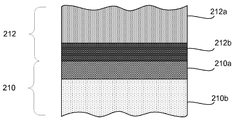
적층체(204)는 또한 ZrO2, TiO2, 또는 Al2O3과 같은 다른 금속 산화물일 수 있는 커플링 층(212), 금속성(metallic) Ti와 같은 금속성 층, 또는 Ti 및 TiO2를 포함하는 층을 포함할 수 있다. 다른 실시예들에서, 커플링 층(212)은 인접한 전극(208)의 증착시 또는 어닐링(annealing)시에 부분적으로 또는 완전히 산화되는 금속 층으로서 증착될 수 있다. 커플링 층(212)은 예를 들어, 전극(208) 부근에서 결함들을 생성함으로써 전극(208)에서의 변화를 촉진할 수 있다. 예를 들면, 커플링 층이 어닐링(급속 열 산화 또는 진공 어닐(anneal)과 같은) 동안에 Ti와 같은 금속이라면, 커플링 층(212)은 인접한 금속 산화물 변화 층(210)으로부터 산소를 끌어당길 수 있고, 이에 의해 커플링 층(212)을 산화하는 한편 변화 층(210)에서 산소 공극들을 생성한다.The laminate 204 also includes a
예를 들어, 도 2b에 도시된 바와 같이, 메모리 소자(102)는 증착되는 실질적으로 금속성 티타늄(또는 다른 금속)인 커플링 층(212), 및 금속 산화물(예를 들어, HfO2)인 변화 층을 포함한다. 메모리 소자(102)가 어닐된 후 또는 전극(208)의 증착의 결과로서, 금속성 커플링 층(212)은 변화 층(210)으로부터 산소를 끌어당길 수 있으며, 커플링 층(210)과 변화 층(210)에서 다른 특징들(예를 들어, 다른 산소 농도들(concentrations))을 갖는 다수의 부분들을 갖는 것으로 초래된다. 예를 들면, 커플링 층(212)의 제 1 부분(212a)은 실질적으로 금속성(예를 들어, 실질적으로 금속성 티타늄)인 반면에, 변화 층(210)과 접촉하는 제 2 부분(212b)은 실질적으로 금속 산화물(예를 들어, 티타늄 산화물)이다. 동시에, 커플링 층(212)과 접촉하는 변화 층(210)의 제 1 부분(210a)은 금속 산화물에 있는 산소가 커플링 층(212)의 제 2 부분(212b)으로 이동하기 때문에 산소 부족(deficient)이고, 변화 특징들을 조정하기 위해 사용될 수 있는 산소 공극들을 떠난다. 변화 층(210)의 제 2 부분(210b)은 제 1 부분(210b)의 것보다 높은 산소 농도를 갖는다. 다른 한편, 제 1 부분(210a)은 제 2 부분(예를 들어, HfO1 .6-2.0)보다 더 많은 금속 리치(metal-rich)(예를 들어, HfO1 .2-1.5)이다. 부분들(210a, 210b, 212a, 및 212b)은 단지 도시만 되어 있고, 변화 층(210)과 커플링 층(212) 각각은 산소의 상이한 농도들을 갖는 여러 부분들을 가질 수 있거나, 또는 산소 농도가 층들(210, 212)의 두께를 통해 변하게 될 수 있는 것이 이해된다. 더욱이, 커플링 층(212)의 산화 량과 변화 층(210)의 산소의 환원은 어닐의 파라메터들(parameters)(예를 들어, 지속성, RTO를 위한 산소 농도)을 변경함으로써 조정될 수 있다.For example, as shown in FIG. 2B,
커플링 층(212)은 저항-변화 층(210)보다 얇을 수 있고, 예를 들어 커플링 층(212)은 저항-변화 층(210)의 두께보다 25% 작은 두께, 또는 저항-변화 층(210)의 두께보다 10% 작은 두께를 가질 수 있다. 예를 들면, 저항-변화 층(210)은 20-60Å 층일 수 있고, 계면 층(212)은 5-20Å 층일 수 있다.The
몇몇 실시예들에서 커플링 층(212)은 변화 층(210)의 밴드갭과 대략 동일 또는 보다 큰 밴드갭을 갖는다. 커플링 층(212)의 보다 큰 밴드갭은 변화 층(210)으로부터의 누설(leakage)을 감소시킴으로써 메모리 소자(102)의 개선된 유지성(retention)을 도울 수 있다. 부가적으로, 커플링 층(212)은 변화시 보조할 수 있는 전극(커플링 층과 변화 층(210) 사이의 계면 부근에서 또는 계면에서 및/또는 전극(208)과 커플링 층(212) 사이의 계면 부근에서 또는 계면에서 포함함) 부근에서 결함들을 생성할 수 있다. 커플링 층(212)은 변화 층(210)에서 결함들에 액세스(access)를 제공하기에 충분히 얇다.In some
몇몇 실시예들에서, 커플링 층(212)은 증착되는 금속성 티타늄이고, 이 티타늄은 몇몇 실시예들에서 어닐 동안에 적어도 부분적으로 티타늄 산화물일 수 있다. 티타늄 커플링 층(212)은 변화 특징들(예를 들어, 누설을 감소시킴)을 수정하기 위해 사용될 수 있는 인접한 전극(208)의 효과적인 일 함수(work funcion)를 변경할 수 있다.
In some embodiments,
c. 계면 층(Interface Layer)c. Interface Layer
적층체(204)는 전극(206)과 변화 층(210) 사이의 계면 층(214)을 부가로 포함할 수 있다. 계면 층(214)은 변화 층(210)의 증착 동안에 및 결과로, 예를 들어 처리 공정 동안에 열 산화의 결과로 형성되는 전극(206) 물질의 산화물일 수 있다. 계면 층(214)을 몇몇 실시예들에서 변화 층(210)에서 결함들을 바꿀 수 있다(도 8a 내지 도 8b 참조). 다른 실시예들에서, 형성 전압을 감소시키기 위해 또는 변화를 가능하게 하기 위해 계면 층(214)을 제거하는 것이 바람직할 수 있다. 몇몇 실시예들에서, 계면 층(214)은 트랩들이 충전되는 것을 가능하게 변화 층(210) 안으로 효과적인 전자 주입을 방해할 수 있고, 이에 의해 형성 전압을 증가 또는 이를 가로질러 과도한 잠재적 드롭(drop)을 야기하며, 변화 층(210)에서 높은 전기장들(electric fields)을 생성하여 변화를 방지하는 것으로 간주된다. 계면 층(214)의 사이즈를 제어하기 위한 또는 계면 층(214)을 제거하기 위한 기술들은 도 13 및 도 14에 기재된다.The
도 3 및 도 4는 계면 층(214)을 갖는(도 3) 및 갖지 않는(도 4) 메모리 소자에서 에너지 레벨들을 도시한 밴드 다이아그램들(band diagrams)(300, 400)이다. 밴드 다이아그램들(300, 400)의 각각을 위해, 메모리 소자(102)의 임의의 영역 내에 전기장의 강도를 도시하는 대응하는 전기장 다이아그램들(320, 340)이 있다.3 and 4 are band diagrams 300 and 400 showing energy levels in a memory device with and without an interface layer 214 (FIG. 3). For each of the band diagrams 300, 400, there are corresponding electric field diagrams 320, 340 showing the strength of the electric field in any region of the
밴드 다이아그램(300)에서, 메모리 소자는 티타늄 질화물 전극(302), 지르코늄 산화물 커플링 층(304), 하프늄 산화물 변화 층(306), 실리콘 산화물 계면 층(308), 및 n-형 폴리실리콘 전극(310)을 갖는다. 본 명세서에 사용된 물질들이 도시되고; 다른 물질들이 또한 사용될 수 있는(예를 들어, 지르코늄 산화물 대신에 Ti/TiO2, 또는 금속성 티타늄) 것이 이해된다. 밴드 다이아그램(400)에서, 메모리 소자는 티타늄 질화물 전극(402), 지르코늄 산화물 커플링 층(404), 하프늄 산화물 변화 층(406), 및 n-형 폴리실리콘 전극(408)을 갖는다. 전기장 다이아그램(320)에 도시된 바와 같이, 전기장은 계면 층(314)에서 많은 양(322)으로 감소된다. 증가된 변화 전압들은 계면 층(214)에서 전기장 감소를 극복하기 위한 필요성이 있을 수 있다. 계면 층(214)이 충분히 두껍다면, 전체 전기장은 전체적으로 변화를 방지할 수 있는 계면 층(214)에서 손실될 수 있다. 대안적으로, 전기장 다이아그램(420)으로 도시된 바와 같이, 계면 층(214)이 없는 메모리 소자에서 전기장은 변화 전압을 감소하고 더 예측가능한 변화로 초래될 수 있는 변화 층(210)에 포함되는 메모리 소자(102)를 통해 균일하게(422) 감소된다. 그러나, 도 8a 및 도 8b에 관해 기재되는 바와 같이, 변화 층(210)에서 결함들의 수를 증가시키기 위해 제어된-두께 계면 층(214)을 유지하는 것이 바람직할 수 있다.In the band diagram 300, the memory element is a
도 5는 계면 층(214)의 존재시 형성 전압의 종속관계(dependency)를 도시하는 그래프이다. 세 세트의 메모리 소자들이 준비된다:5 is a graph showing the dependency of the formation voltage in the presence of the
다이아몬드(502)로 나타내 제 1 세트의 메모리 소자들은 티타늄 질화물 전The first set of memory elements, represented by
극(206), PVD-증착된 하프늄 산화물 변화 층(210), 및 커플링 층(212)이
없는 백금 전극(208)을 포함한다.A
사각형(504)으로 나타낸 제 2 세트의 메모리 소자들은 n-형 폴리실리콘 전극The second set of memory elements, represented by the
(206), ALD-증착 하프늄 산화물 변화 층(210), 및 커플링 층(212)이 없는206, without ALD-deposited hafnium
티타늄 질화물 전극(208)을 포함한다.
원(506)으로 나타낸 제 3 세트의 메모리 소자들은 n-형 폴리실리콘 전극The third set of memory elements represented by
(206), PVD-증착된 하프늄 산화물 변화 층(210), 및 커플링 층(212)이 206, PVD-deposited hafnium
없는 백금 전극(208)을 포함한다.A
그래프(500)는 메모리 소자들에서 변화 층의 두께의 함수로서 메모리 소자들의 중간 형성 전압을 도시한다. 도시된 바와 같이, 동일한 두께를 갖는 변화 층을 위해, 티타늄 질화물 상에서 PVD 하프늄 산화물을 포함하는 소자들(502)은 가장 낮은 형성 전압을 갖고, 폴리실리콘 상에서 PVD 하프늄 산화물을 포함하는 소자들(506)은 다음으로 낮은 형성 전압을 가지며, 폴리실리콘 상에서 ALD 하프늄 산화물을 갖는 소자들(504)은 가장 높은 형성 전압을 갖는다. ALD 공정들은 증가된 형성 전압들로 유도되는 잠재적으로 보다 높은 프로세싱(processing) 온도들(PVD의 몇몇 실예를 위한 200℃ 이상 대 실온) 때문에 적어도 부분적으로 보다 두꺼운 계면 층(214)을 형성하기 위해 더 가능하다고 간주된다. 부가적으로, 폴리실리콘 전극들(예를 들어, 소자들(502, 506)) 상에 생성된 실리콘 산화물 계면 층(214)은 티타늄 질화물과 같은 금속-함유 전극 상에 생성된 산화물보다 전도성이 낮다. 따라서, 계면 층(214), 특히 실리콘계 전극들을 감소 및/또는 제어하기 위한 기술들은 형성 전압들을 개선하기 위해 사용될 수 있다.
ALD 공정이 보다 두꺼운 계면 층들(214)을 형성하기 위해 더 용이할 수 있고 증가된 형성 전압들을 갖는 메모리 소자들로 초래될 지라도, 이는 다른 이유들(예를 들어, 더 등각적인(conformal) 층을 형성하기 위해)을 위해 PVD 프로세싱 위에 ALD 프로세싱을 사용하는 것이 바람직할 것이고, 도 13은 ALD 프로세싱을 사용하는 계면 층(214)을 감소 또는 제거하기 위한 공정을 설명한다. 부가적으로, 도 8a 및 도 8b와 관련하여 설명된 바와 같이, 이는 또한 도 13의 공정을 사용하여 형성될 수 있는 변화 층(210)에서 결함들의 수를 증가시키기 위해 제어된-두꺼운 계면 층(214)(예를 들어, 10Å 이하)을 유지하는 것이 바람직할 수 있다.Although the ALD process may be easier to form thicker
계면 층(214)을 갖는 것이 바람직하다면, MIM 적층체(204)의 층들의 증착의 순서가 중요할 수 있다. 계면 층(214)이 변화 층(210)의 증착 동안에 형성되므로, 변화 층(210)은 계면 층(214)이 (예를 들어, 실리콘 산화물 계면 층(214)이 바람직하다면 폴리실리콘 층 상에 형성됨) 형성되는 전극 상에 형성될 수 있다. 실예로서 그리고 도 7에 부가로 논의된 바와 같이, 3-차원 메모리 어레이를 형성할 시에, 이는 다른 소자들의 배향이 역전될 때에도 동일한 배향(예를 들어, 항상 바닥 상에 있는 하나의 전극)으로 메모리 소자를 항상 형성하기 위해 필요할 수 있다. 그러나, 다른 실시예들에서, 계면 층(214)은 메모리 소자(102)가 메모리 소자(102)의 후 증착 어닐을 사용함으로써 역전 순서로 증착될 때에 생성될 수 있다.
If it is desired to have the
d. 전극들(Electrodes)d. Electrodes
전극들(206, 208)은 서로 다른 물질들일 수 있다. 몇몇 실시예들에서, 전극들은 0.1과 1 전자 볼드(eV) 사이, 또는 0.4와 0.6 eV 사이 등에 의해 다른 일 함수를 갖는다. 예를 들면, 전극(208)은 4.5-4.6 eV의 일 함수를 갖는 TiN일 수 있는 한편, 전극(206)은 대략 4.1-4.5 eV의 일 함수를 갖는 n-형 폴리실리콘일 수 있다. 다른 전극 물질들은 p-형 폴리실리콘(4.9-5.3 eV), 전이 금속들(transition metals), 전이 금속 합금들, 전이 금속 질화물들, 전이 금속 카바이드들, 백금(5.7 eV), 텅스텐(4.5-4.6 eV), 탄탈륨 질화물(4.7-4.8 eV), 몰리브덴 산화물(대략 5.1 eV), 몰리브덴 질화물(4.0-5.0 eV), 이리듐(4.6-5.3 eV), 이리듐 산화물(대략 4.2 eV), 루테늄(대략 4.7 eV), 및 루테늄 산화물(대략 5.0 eV)를 포함한다. 다른 잠재적 전극들은 티타늄/알루미늄 합금(4.1-4.3 eV), 니켈(대략 5.0 eV), 텅스텐 질화물(대략 4.3-5.0 eV), 텅스텐 산화물(5.5-5.7 eV), 알루미늄(4.2-4.3 eV), 구리 또는 실리콘-도핑된 알루미늄(4.1-4.4 eV), 구리(대략 4.5 eV), 하프늄 카바이드(4.8-4.9 eV), 하프늄 질화물(4.7-4.8 eV), 니오븀 질화물(대략 4.95 eV), 탄탈륨 카바이드(대략 5.1 eV), 탄탈륨 실리콘 질화물(대략 4.4 eV), 티타늄(4.1-4.4 eV), 바나듐 카바이드(대략 5.15 eV), 바나듐 질화물(대략 5.15 eV), 및 지르코늄 질화물(대략 4.6 eV)을 포함한다. 본 명세서에 설명된 몇몇 실시예들에서, 보다 높은 일 함수 전극은 비록 다른 형상들이 가능할지라도, 재설정 동작 동안에 양의 펄스(positive pulse)(공통 기준 전위와 비교하여 측정된 바와 같음)를 수신한다. 다른 실시예들에서, 보다 높은 일 함수 전극은 재설정 동작 동안에 음(negative)의 펄스를 수신한다. 몇몇 실시예들에서, 메모리 소자들(102)은 설정 및 재설정 전압들이 공통 전기적 기준(electrical reference)에 대해 반대 극성들(opposite polarities)을 갖는 곳에서 바이폴라(bipolar) 변화를 사용하고, 일부 실시예들에서 메모리 소자들(102)은 설정 및 재설정 전압들이 동일 극성을 가지는 곳에서 유니폴라(unipolar) 변화를 사용한다. 다른 실시예들에서, 이는 누설을 감소시키고 더 안정한 금속 산화물/전극 계면을 생성하기 위하여 전극들의 일 함수를 일반적으로 증가시키는 것이 바람직하다.
The
2. 선택 소자들(Select Elements)2. Select Elements
다이오드(202)는 메모리 어레이(100)의 몇몇 메모리 소자들(102)(도 1 참조)과 같은 여러 메모리 소자들 사이에서 액세스(access)를 위한 메모리 소자를 선택하기 위해 사용될 수 있는 선택 소자이다. 다이오드(202)는 전류만이 메모리 소자들(102)을 통해 일 방향으로 흐르도록 전류의 흐름을 제어한다.
다이오드(202)는 반도체 물질의 두 개 이상의 층들을 포함할 수 있다. 다이오드는 일반적으로 p-n 접합(junction)이고, 도핑된 실리콘 층들(216, 218)은 p-n 접합을 형성할 수 있다. 예를 들면, 도핑된 실리콘 층(216)은 p-형 층일 수 있고, 도핑된 실리콘 층(218)은 n-형 층일 수 있으므로, 다이오드(202)의 노드(node)(220)는 애노드(anode)이고 제 1 전극(206)에 연결된다. 이러한 실예에서, 다이오드(202)의 노드(222)는 캐소드(cathode)이고 신호 라인(106)에 연결되며, 이 신호 라인은 예를 들어, 비트 라인 또는 워드 라인일 수 있거나, 또는 비트 라인 또는 워드 라인에 연결된다. 노드들(220, 222)은 메모리 소자(102)에서 물리적 특징이 필수적이지 않고, 예를 들어 전극(206)은 도핑된 실리콘 층(216)과 직접 접촉할 수 있다. 다른 실시예들에서, 저 저항성 필름과 같은 하나 이상의 부가적인 층들은 전극(206)과 도핑된 실리콘 층(216) 사이에 부가된다.
몇몇 실시예들에서, 도핑된 실리콘 층(216)은 n-형 층이고, 도핑된 실리콘 층(218)은 p-형 층이며, 노드(220)는 다이오드(202)의 캐소드이고, 노드(222)는 다이오드(202)의 애노드이다. 임의의 절연 층(214)은 p-i-n 또는 n-i-p 다이오드(202)를 생성하기 위해 도핑된 실리콘 층들(216, 218) 사이에 있을 수 있다. 일부 실시예들에서, 절연층(214)과 도핑된 실리콘 층들(216, 218) 중 하나는 동일 층으로 형성된다. 예를 들면, 실리콘 층이 증착될 수 있고, 이 층의 일 부분은 도핑된 실리콘 층(216 또는 218)을 형성하기 위해 도핑될 수 있다. 그런 다음, 상기 층의 나머지 부분은 절연 층(214)이다.In some embodiments, doped
다른 실시예들에서, 메모리 소자(102)의 일 전극은 다이오드(202)의 일 부분으로서 또한 작용할 수 있는 도핑된 실리콘(예를 들어, p-형 또는 n-형 폴리실리콘)일 수 있다. 도 6은 선택 소자로서 사용되는 다이오드를 갖는 전극을 공유하는(shares) 메모리 소자를 도시한다. 다이오드(202)가 도핑된 실리콘의 두 층들로 이루어지므로, 그리고 도핑된 실리콘의 층이 메모리 소자(102)의 전극으로서 사용될 수 있다면, 도핑된 실리콘의 단일 층(예를 들어, n-형 폴리실리콘의 층)은 메모리 소자(102)의 전극으로서 그리고 다이오드(202) 층으로서 작용할 수 있다. 다이오드(202)와 메모리 소자(102) 사이에서 도핑된 실리콘 층을 공유함으로써, 다이오드(202)와 메모리 소자(102) 사이의 두 층들, 즉 도핑된 실리콘 층과 커플링 층, 및 관련된 프로세싱 단계들은 제거될 수 있다.
In other embodiments, one electrode of
3. 변화 극성(Switching Polarity)3. Switching Polarity
신호 라인(예를 들어, 신호 라인(104))은 "제 2" 전극(208)에 연결되고, 이 신호 라인은 변화 전압들을 제 2 전극(208)에 제공하기 위해 형성된다. 몇몇 실시예들에서, 제 2 전극(208)은 제 1 전극(206)보다 보다 높은 일 함수를 갖고, 신호 라인(104)은 공통 전기적 기준에 대해 음의 설정 전압과, 공통 전기적 기준에 대해 양의 재설정 전압을 제공하기 위해 형성된다. 이 실시예들은 보다 낮은 일 함수 제 1 전극(206)(예를 들어, 티타늄 질화물)과 백금 또는 루테늄과 같은 보다 높은 일 함수 제 2 전극을 사용하는 이들을 포함한다. 예를 들면, 공통 전기적 기준은 접지(ground)(즉, 0V)일 수 있고, 그런 다음 설정 전압은 음의 전압(예를 들어, -2V)일 수 있으며, 재설정 전압은 양의 전압(예를 들어, 2V)일 수 있다. 그러나, 공통 전기적 기준은 +2V 또는 -2V와 같은 임의의 전압일 수 있다.A signal line (eg, signal line 104) is connected to the “second”
다른 실시예들에서, 제 2 전극(208)은 또한 제 1 전극(206)보다 보다 높은 일 함수를 갖고, 신호 라인(104)은 공통 전기적 기준에 대해 양의 설정 전압과 음의 재설정 전압을 제공하기 위해 형성된다. 예를 들면, 도핑된 실리콘 제 1 전극(206)(예를 들어, n-형 폴리실리콘)과 보다 높은 일 함수 제 2 전극(208)(예를 들어, 티타늄 질화물)을 갖는 메모리 소자에서, 재설정 전압은 제 2 전극(208)에서 음수 일 수 있다. 예를 들어, 도 16a 및 도 16b 참조.In other embodiments, the
몇몇 실시예들에서, 메모리 소자의 하나의 변화 전압(예를 들어, 재설정 전압)은 공통 전기적 기준에 대해 제 1 극성(예를 들어, 양의 극성)을 가질 수 있고, 다른 변화 전압(예를 들어, 설정 전압)은 메모리 소자가 바이폴라 변화를 사용하도록 공통 전기적 기준에 대해 음의 극성을 가질 수 있다. 다른 실시예들에서, 변화 전압들은 공통 기준에 대해 동일 극성을 갖고 유니폴라 변화으로 언급된다. 몇몇 실시예들에서, 이는 메모리 어레이(예를 들어, 선택 소자들)의 다른 소자들의 임의의 형상에 양립성(compatibility)을 제공하기 위한 유니폴라 변화가 바람직하다. 부가적으로, 변화 전압들은 예를 들어, 1ms 미만, 50㎲ 미만, 1㎲ 미만, 50ns 미만 등의 제한된 내구성(limited duration)을 갖는 전압 펄스들(예를 들어, 사각파 펄스들)일 수 있다.
In some embodiments, one change voltage (eg, reset voltage) of the memory element may have a first polarity (eg, positive polarity) relative to a common electrical reference, and the other change voltage (eg, For example, the set voltage) may have a negative polarity with respect to a common electrical reference such that the memory device uses a bipolar change. In other embodiments, the change voltages have the same polarity with respect to a common reference and are referred to as unipolar change. In some embodiments, this is desirable for unipolar variations to provide compatibility with any shape of other elements of the memory array (eg, select elements). Additionally, the change voltages can be voltage pulses (eg, square wave pulses) with limited duration, such as less than 1 ms, less than 50 ms, less than 1 ms, less than 50 ns, and the like. .
4. 형성 전압의 극성(Polarity of Forming Voltage)4. Polarity of Forming Voltage
낮은 동작 전압들은 메모리 어레이에서 관련된 디바이스들(예를 들어, 다이오드들)을 보호하기 위한 저항 변화 메모리 소자들을 위해 바람직하다. 형성 전압은 종종 가장 높은 크기의 동작 전압이고, 따라서 형성 전압의 감소는 디바이스 동작 및 신뢰성을 개선하기 위한 중요한 목표이다. 형성 전압 극성은 몇몇 실시예들에서 형성 전압 크기에 영향을 미치는 것으로 도시되어 있다.Low operating voltages are desirable for resistive change memory elements to protect related devices (eg diodes) in a memory array. The formation voltage is often the highest magnitude of operating voltage, and thus the reduction of the formation voltage is an important goal for improving device operation and reliability. The formation voltage polarity is shown to affect the formation voltage magnitude in some embodiments.
하나의 예시에서, 메모리 소자들은 접지에 연결된 보다 높은 일 함수 전극과 형성 전압 펄스를 수신하는 보다 낮은 일 함수 전극을 준비한다. 제 1 실예는 n-형 폴리실리콘 전극, 하프늄 산화물 변화 층 및 티타늄 질화물 전극을 포함한다. 이 예시에서, 티타늄 질화물 전극(즉, 보다 높은 일 함수 전극)은 접지되어 양 및 음 형성 전압 펄스들은 n-형 폴리실리콘 전극에 인가된다. 음 펄스들은 대략 -8V의 중간 형성 전압을 갖는 반면에, 양 펄스들은 대략 +13V의 중간 형성 전압을 갖는다. 제 2 예시에서 메모리 소자는 티타늄 질화물 전극, 하프늄 산화물 변화 층, 및 백금 전극을 준비한다. 보다 높은 일 함수 전극(여기서, 백금 전극)은 접지되고, 보다 낮은 일 함수 전극(티타늄 질화물 전극)은 형성 전압 펄스들을 수신한다. 이 예시에서, 음 펄스들의 중간 형성 전압은 -4.4V인 반면에, 양 펄스들을 사용하는 중간 형성 전압은 6.4V이다.In one example, the memory devices prepare a higher work function electrode connected to ground and a lower work function electrode that receives the forming voltage pulse. The first example includes an n-type polysilicon electrode, a hafnium oxide change layer and a titanium nitride electrode. In this example, the titanium nitride electrode (ie, higher work function electrode) is grounded so that positive and negative forming voltage pulses are applied to the n-type polysilicon electrode. Negative pulses have an intermediate forming voltage of approximately -8V, while positive pulses have an intermediate forming voltage of approximately + 13V. In the second example, the memory device prepares a titanium nitride electrode, a hafnium oxide change layer, and a platinum electrode. The higher work function electrode (here platinum electrode) is grounded and the lower work function electrode (titanium nitride electrode) receives the forming voltage pulses. In this example, the intermediate shaping voltage of negative pulses is -4.4V, while the intermediate shaping voltage using positive pulses is 6.4V.
상기 예시들은 보다 낮은 일 함수 전극에 인가된 음 형성 전압이 몇몇 실시예들에서 형성 전압의 크기를 감소할 수 있는 것을 설명되었다. 이는 보다 낮은 일 함수 전극으로부터 전자 주입이 양 극성 형성 전압과 비교하여 음 극성 형성 전압의 크기를 감소할 수 있는 것으로 간주된다.The above examples have been described that the negative forming voltage applied to the lower work function electrode may reduce the magnitude of the forming voltage in some embodiments. It is considered that electron injection from the lower work function electrode can reduce the magnitude of the negative polarity forming voltage compared to the positive polarity forming voltage.
부가적으로, 메모리 소자에서 일 함수의 전극들 사이의 차이가 더 크면 클 수록, 형성 전압의 크기가 더 적게 되는 것을 몇몇 실시예들에 의해 설명된다. 예를 들면, n-형 폴리실리콘 전극, 하프늄 산화물 변화 층 및 티타늄 질화물 전극을 갖는 메모리 소자에서, 일 함수에 있어서의 차이는 대략 0.5 eV이고, 중간 형성 전압은 -7V이다. n-형 폴리실리콘 전극, 하프늄 산화물 변화 층, 및 백금 전극을 갖는 다른 메모리 소자는 1.6 eV의 일 함수 차이와 -5.5V의 중간 형성 전압을 갖는다. 따라서, 일부 실시예들에서, 이는 비록 예시로서 일 함수 차이를 1.6 eV까지 증가시킬 필요가 없을지라도, 형성 전압을 감소시키기 위해 전극들 사이에서 일 함수 차이를 증가시키는 것이 바람직할 수 있다.
Additionally, the greater the difference between the electrodes of the work function in the memory element, the smaller the magnitude of the formation voltage is described by some embodiments. For example, in a memory device having an n-type polysilicon electrode, a hafnium oxide change layer and a titanium nitride electrode, the difference in work function is approximately 0.5 eV, and the intermediate formation voltage is -7V. Other memory devices with n-type polysilicon electrodes, hafnium oxide change layers, and platinum electrodes have a work function difference of 1.6 eV and an intermediate formation voltage of -5.5V. Thus, in some embodiments, it may be desirable to increase the work function difference between the electrodes to reduce the formation voltage, although it is not necessary to increase the work function difference to 1.6 eV by way of example.
5. 다른 특징들(Other Characteristics)5. Other Characteristics
이는 메모리 유지성을 부가하기 위하여 저항-변화 층(210)으로서 저-누설 물질을 갖는 것이 바람직할 수 있다. 예를 들어, 층(210)은 메모리 소자의 오프 상태(off state)(예를 들어, 높은 저항 상태)에서 금속 산화물의 두께의 20옹스트롬(Å)(angstroms) 당 0.5 볼트(V)로 측정된 제곱센티미터 당 40 암페어(40 A/㎠)보다 작은 누설 전류 밀도를 갖는 물질일 수 있다.
It may be desirable to have a low-leakage material as resistance-
6. 3-D 메모리 구조(3-D Memory Structure)6. 3-D Memory Structure
도 7은 본 명세서에 설명된 메모리 소자들(102)을 사용하는 3-차원 메모리 어레이(700)의 일 부분을 도시한다. 어레이(700)는 두 개의 워드 라인들(word lines)(702a, 702b), 및 공유된 비트 라인(shared bit lines)(704)을 포함한다. 두 개의 MIM 적층체들(204a, 204b)과 다이오드들(202a, 204b)은 어레이(700)로 도시되고; 메모리 셀(706a)은 MIM 적층체(204a)와 다이오드(202a)를 포함하며, 메모리 셀(706b)은 MIM 적층체(204b)와 다이오드(202b)를 포함한다.7 illustrates a portion of a three-
메모리 어레이(700)는 두 개의 메모리 셀들(706a, 706b)이 동일한 공유 비트 라인(704)을 사용할 수 있도록 형성된다. 여기에 도시된 바와 같이, MIM 적층체들(204a, 204b) 양자는 동일한 순서로 내장된 그들의 개별 층들(즉, 전극들(206, 208) 및 변화 층(210))을 갖는다. 다른 한편, MIM 적층체들(204a, 204b) 양자를 위해, 전극(206)이 먼저 형성되고, 변화 층(210)은 전극(206)의 상부에 형성되며, 전극(208)은 변화 층(210)의 상부에 형성된다. 상술한 바와 같이, MIM 적층체들(204) 층들의 증착 순서는 계면 층(214)을 생성하기 위하여 동일하게 될 필요가 있다. 그러나, 몇몇 실시예들에서, 증착 순서는 역전될 수 있고, 계면 층(214)은 전극 증착 또는 어닐링과 같은 연속적인 공정들의 결과로서 생성된다.The
다른 한편, 다이오드들(202a, 202b)은 서로 거울대칭(mirrors)이다. 다른 한편, 다이오드(202a)는 바닥부 상에서 층(216)을 갖고, 다이오드(202b)는 바닥부 상에서 층(218)을 갖는다. 예를 들면, 층(216)은 n-형 층일 수 있고, 층(218)은 p-형 층일 수 있다. 이 형상을 사용하여, 다이오드들(202a, 202b)은 반대 방향으로 편향되고, 메모리 셀들(706)은 동일한 공유 비트 라인(704) 양자를 사용하게 한다. 회로 다이아그램들(708a, 708b)로 도시된 바와 같이, 다이오드들은 임의의 필요한 배향을 가질 수 있고, 이 배향은 3-차원 메모리 어레이 형상에 기초하여 다를 수 있다.
On the other hand,
7. 계면 층 및 산소 공극들(Interface Layer and Oxygen Vacancies)7. Interface Layer and Oxygen Vacancies
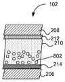
도 8a 및 도 8b는 메모리 소자(102)를 도시하고 계면 층(214)을 사용하는 메모리 소자(102) 내에 산소 공극들(oxygen vacancies)(결함들(defects))의 생성 및 조작(manipulation)을 도시한다. 계면 층(214)은 메모리 소자(102)에서 다른 층들의 프로세싱 동안에 생성될 수 있는 산화물 층이다. 예를 들면, 변화 층(210)의 증착은 계면 층(214)을 생성하기 위한 온도(예를 들어, 200℃ 이상)에서의 프로세싱을 포함할 수 있다. 예를 들어, 전극(206)이 도핑된 실리콘(예를 들어, 폴리실리콘)이라면, 변화 층(210)의 증착(예를 들어, PVD 또는 ALD를 사용)은 실리콘 산화물 계면 층(214)을 생성할 수 있는 온도를 포함할 수 있다. 계면 층(214)은 몇몇 실시예들에선 제거될 수 있으나, 다른 실시예들에서 계면 층(214)은 누설 특징들을 개선함으로써 변화 층(210)의 유지성을 개선하고 변화 층(210)에서 결함들(예를 들어, 산소 공극들)을 조절하기 위해 유지될 수 있다. 계면 층(214)이 유지되는 몇몇 실시예들에서, 계면 층(214)은 전극(206)(즉, 계면 층(214)이 변화 층(210)의 결함들에 액세스를 제공함)에 대해 보이는 결함들을 변화 층(210)에서 만들기 위해 그리고 변화 전압들에서 계면 층(214)의 효과를 감소시키기 위해 비교적 얇을 수 있다(예를 들어, 10Å 이하).8A and 8B illustrate the
일 실예에서, 하부 전극(206)은 폴리실리콘이다. 실리콘은 특히 가열될 시에 산소를 흡인하는 것으로 알려져 있고 금속 산화물 변화 층(210)으로부터 산소를 끌어당길 수 있으며, 금속-리치 금속 산화물 변화 층을 가까이에서 생성하는 변화 층(210)에서 산소 공극들(802)을 떠난다. 이론에 의해 구속되는 일 없이, 이들 산소 공극들(802)은 트랩들(traps)로서 작용할 수 있고, 이 트랩들은 상기 트랩들을 채우고 비우기 위해 프로그래밍(programming) 전압들의 적용으로 전류 흐름을 조절한다. 산소 공극들(802)은 이동될 필요가 없다. 몇몇 실시예들에서, 계면 층(214)의 존재는 프로세싱 조건들에 따라 변화 층(210)의 양 측면 상에 또는 변화 층(210)을 통해서 부가적인 산소 공극들을 생성할 수 있는 산소를 또한 흡인하는 금속성(metallic) 또는 부분적으로 금속성 커플링 층(212)의 존재와 조합될 수 있다.In one embodiment, the
얇은 또는 제로(0) 층간(interlayer) 계면 층(214)은 변화 층(210)에서 산소 공극들(802)의 밀도를 조절하기 위해 사용될 수 있다. 예를 들면, 더 얇은 계면 층(214)(예를 들어, 5Å 대 10Å)은 산소 공극(802) 밀도를 증가시킬 수 있다. 부가적으로, 변화 층(210)의 두께는 트랩들(예를 들어, 산소 공극들(802))이 변화 층(210)을 통해서 공간적으로 더 균등하게 되도록 최적화될 수 있다. 예를 들면, 도 8a는 계면 층(214) 부근에 집중된 산소 공극들(802)을 갖는 보다 두꺼운 변화 층(210)을 도시하는 반면에, 도 8b는 산소 공극들(802)의 더 균일한 분포를 갖는 더 얇은 변화 층(210)을 갖는다. 예를 들어, 동일한 물질들을 사용하는 두 개의 메모리 소자들에서, 도 8a의 변화 층(210)은 50Å인 반면에, 도 8b에서 변화 층(210)의 두께는 25Å이다. 변화 층(210) 내의 산소 공극들(802)의 분포는 사용된 물질들, 계면 층(214)의 두께, 사용된 공정들(예를 들어, 사용된 어닐들(anneals)의 온도) 등을 포함하는 여러 인자들에 의존할 수 있다. 도 8a 및 도 8b는 산소 공극 분포의 두 예시만을 도시하고, 이는 다양한 다른 형상들이 가능하다는 것이 이해된다.
A thin or zero interlayer
Ⅲ. 메모리 동작(III. Memory behavior ( MenoryMenory OperationOperation ))
판독 동작 중에, 메모리 소자(102)의 상태는 감지 전압(즉, "판독(read)" 전압 VREAD)을 적합한 세트의 신호 라인들(104, 106)에 인가함으로써 감지될 수 있다. 이 이력에 따르면, 이러한 방식으로 어드레스되는(addressed) 메모리 소자는 고 저항 상태 또는 저 저항 상태일 수 있다. 따라서, 메모리 소자의 저항은 디지털 데이터가 메모리 소자에 의해 얼마나 저장되는지를 결정한다. 메모리 소자가 저 저항을 갖는다면, 예를 들어 메모리 소자는 논리 1(logic one)(즉, "1" 비트)을 함유하는 것이라고 말할 수 있다. 다른 한편, 메모리 소자가 고 저항을 갖는다면, 메모리 소자는 논리 제로(0)(즉, "0" 비트)를 함유하는 것이라고 말할 수 있다. 기입(write) 동작 중에, 메모리 소자의 상태는 적합한 세트의 신호 라인들(104, 106)에 적합한 기입 신호들의 적용에 의해 변경될 수 있다.During a read operation, the state of the
도 9는 메모리 소자(102)에 대한 전류(I) 대 전압(V)의 대수 관계 구상도(900)이다.9 is a logarithmic relational diagram 900 of current I versus voltage V for
도 9는 메모리 소자(102)의 콘텐츠를 변경하기 위해 설정 및 재설정 동작을 도시한다. 처음에, 메모리 소자(102)는 고 저항 상태("HRS", 예를 들어 논리 0을 저장함)일 수 있다. 이 상태에서, 메모리 소자(102)의 전류 대 전압 특징들은 실선 HRS(902)로 도시된다. 메모리 소자(102)의 고 저항 상태는 신호 라인들(104, 106)을 사용하여 판독 및 기입 회로에 의해 감지될 수 있다. 예를 들어, 판독 및 기입 회로는 판독 전압 VREAD를 메모리 소자(102)에 인가할 수 있고, 메모리 소자(102)를 통해 흐르는 결과적인 "오프(off)" 전류 IOFF를 감지할 수 있다. 메모리 소자(102)에 논리 1을 저장하기를 원할 때, 메모리 소자(102)는 그 저 저항 상태에 배치될 수 있다. 이는 신호 라인들(104, 106)을 가로질러 설정 전압 VSET을 인가하기 위해 판독 및 기입 회로를 사용함으로써 달성될 수 있다. VSET를 메모리 소자(102)에 인가하는 것은 메모리 소자(102)가 점선(906)으로 지시된 바와 같이 그 저 저항 상태로 변화되게 한다. 이 영역에서, 메모리 소자(102)는, 설정 전압 VSET의 제거에 이어서 메모리 소자(102)가 저 저항 곡선 LRS(904)로 특징지어지도록 변경된다. 하기에 더 설명되는 바와 같이, 메모리 소자(102)의 저항 상태의 변경은 금속 산화물 물질에서 트랩들의 충전때문일 수 있다(즉, "트랩-조정(trap-mediate)"될 수 있다). VSET 및 VRESET는 일반적으로 "변화 전압들(switching voltages)"로 언급될 수 있다.9 illustrates setup and reset operations to change the content of
메모리 소자(102)의 저 저항 상태는 판독 및 기입 회로를 사용하여 감지될 수 있다. 판독 전압 VREAD가 저항 변화 메모리 소자(102)에 인가될 때에, 판독 및 기입 회로는 메모리 소자(102)가 그 저 저항 상태에 있다는 것을 지시하는 비교적 높은 "온(on)" 전류 값 ION을 감지할 것이다. 메모리 소자(102)에 논리 0을 저장하기를 원할 때에, 메모리 소자는 재설정 전압 VRESET을 메모리 소자(102)에 인가함으로써 그 고 저항 상태에 다시 한 번 배치될 수 있다. 판독 및 기입 회로가 VRESET을 메모리 소자(102)에 인가할 때에, 메모리 소자(102)는 점선(908)으로 지시된 바와 같이 그 고 저항 상태 HRS로 진입한다. 재설정 전압 VRESET이 메모리 소자(102)로부터 제거될 때, 메모리 소자(102)는 고 저항 라인 HRS(904)에 의해 다시 한 번 특징지어질 것이다. 전압 펄스들은 메모리 소자(102)의 프로그래밍 시에 사용될 수 있다. 예를 들어, 1ms, 10㎲, 5㎲, 500ns 등의 사각형 펄스는 메모리 소자(102)를 변화하기 위해 사용될 수 있고; 몇몇 실시예들에서, 메모리 소자(102)를 변화하기 위해 요구되는 시간이 양에 따라 펄스의 길이를 조절하는 것이 바람직할 수 있다.The low resistance state of
형성 전압 VFORM은 메모리 소자(102)를 사용하기 위해 준비하여 메모리 소자(102)에 인가되는 전압이다. 본 명세서에 기재된 몇몇 메모리 소자들은 설정 전압 또는 재설정 전압 이상의 전압의 인가를 포함하는 형성 이벤트(forming event)를 필요로 할 수 있다. 일단 메모리 소자(102)가 처음 변화되면, 설정 및 재설정 전압들은 메모리 소자(102)의 저항 상태를 변경하기 위해 사용될 수 있다.The formation voltage V FORM is a voltage prepared for use of the
저항 변화 메모리 소자(102)의 쌍안정 저항(bistable resistance)은 디지털 데이터를 저장하기 위해 적합한 메모리 소자(102)를 만든다. 전압들 VSET 및 VRESET의 인가 결여 시에 저장된 데이터에 어떠한 변경도 발생하기 않기 때문에, 소자(102)와 같은 소자들로부터 형성되는 메모리는 비-휘발성(non-volatile)이다.The bistable resistance of the resistive
도 10은 저항 상태 변경을 설명하는 메모리 소자(102)에 대한 전류(I) 대 전압(V)의 구상도(1000)이다. 구상도(1000)는 메모리 소자(102)에 인가되는 전압 램프(voltage ramp)를 x 축에 도시하고 결과적인 전류를 y 축에 나타낸다. 라인(1002)은 램프형 전압이 인가될 때 저항 물질(Ohmic material)의 응답을 나타낸다. 저항 응답은 바람직하지 않은데, 이는 설정 또는 재설정이 발생하는 어떠한 이산(discrete) 전압도 없기 때문이다.FIG. 10 is a schematic diagram 1000 of current I versus voltage V for
일반적으로, 그래프(1004)와 같은 보다 급작스러운 응답이 요망된다. 그래프(1004)는 저항 응답(1004a)으로 시작하여 날카롭게 위로 향해(1004b) 만곡된다. 그래프(1004)는 메모리 소자(102)가 HRS(902)로부터 LRS(904)로 변화되는 설정 동작을 나타낼 수 있다.In general, a more abrupt response, such as graph 1004 is desired. The graph 1004 begins with the
이론에 의해 구속되는 일 없이, 비-금속 투과 경로들(percolation paths)은 설정 동작 동안에 형성되고 재설정 동작 동안에 파괴된다. 예를 들어, 설정 동작 동안에, 메모리 소자(102)는 저 저항 상태로 변화된다. 트랩들을 충전시킴으로써 형성되는 투과 경로들은 금속 산화물의 전도성을 증가시키고, 그에 의해 저항성을 감소(즉, 변경)시킨다. 404b로 도시된 전압은 설정 전압이다. 설정 전압에서, 트랩들이 충전되고, 금속 산화물의 저항이 감소함에 따라 전류가 크게 상승한다.
Without being bound by theory, non-metallic percolation paths are formed during the setting operation and destroyed during the resetting operation. For example, during the setting operation, the
Ⅳ. 물질들(Ⅳ. Substances MaterialsMaterials ))
금속 산화물들의 다양성은 본 명세서에 기재된 메모리 소자들(102)의 변화 층(210)을 위해 사용될 수 있다. 몇몇 실시예들에서, 메모리 소자들(102)은 벌크-변화(bulk-switching) 특성들을 나타내고 측정할 수 있다. 다른 한편, 이는 결함들이 변화 층(210)의 벌크를 통해서 분포되고, 변화 전압들(즉, VSET 및 VRESET)이 금속 산화물 두께의 증가 또는 감소에 따라 증가 또는 감소하는 것으로 간주된다. 다른 실시예들에서, 메모리 소자들(102)은 계면-중재(interface-mediated) 변화 활성화를 나타낸다. 다른 실시예들은 벌크- 및 계면-중재 변화 특성들의 조합을 나타낼 수 있고, 이 특성은 계면 층들에서 결함 활성화를 나타낼 것이다.
A variety of metal oxides can be used for the
A. A. 변화 층을Changing floors 위한 보다 높은Higher than 밴드갭Band gap 물질들( Substances HigherHigher -- BandgapBandgap MaterialsMaterials forfor Switching Switching LayerLayer ))
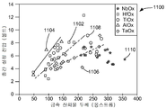
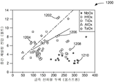
도 11 및 도 12는 본 명세서에 기재된 메모리 소자들에 사용되는 여러 가지 물질들(금속 산화물들)에 대한 금속 산화물 층의 두께들과 결과적인 설정 전압들(set voltages), 재설정 전압들(reset voltages), 및 온/오프 전류 비율들 사이의 관계를 도시하는 그래프이다. 이들 그래프들은 2개의 전극들 및 이들 사이에 배치되는 금속 산화물의 단일 층(즉, 커플링 층(212)이 없음)을 포함하는 메모리 소자의 특징을 도시하고, 임의의 물질들이 벌크-변화 특징들을 나타내는 것을 지시한다. 도 11에서 알 수 있는 바와 같이, 하프늄 산화물(1102), 알루미늄 산화물(1104), 또는 탄탈륨 산화물(tantalum oxide)(1106)을 포함하는 메모리 소자에 대해서, 설정 전압은 두께에 따라 증가하며(즉, 두께에 의존하며), 몇몇 실시예에서 이들 물질들에 대해, 설정 전압은 메모리 소자 내에서 100 옹스트롱(Å)의 금속 산화물 층의 두께 당 적어도 1볼트(V)이다. 몇몇 실시예들에서, 100Å의 금속 산화물 층의 두께 증가는 설정 전압을 적어도 1V만큼 증가시킨다. 마찬가지로, 도 12에 도시한 바와 같이, 하프늄 산화물(1202), 알루미늄 산화물(1204), 또는 탄탈륨 산화물(1206)에 대한 재설정 전압도 두께에 의존한다. 따라서, 이들 데이터는 이들 물질들에 대한 벌크 제어 설정/재설정 메커니즘(bulk-controlled set/reset mechanism)을 지원하는데, 이는 선형 관계가 금속 산화물의 벌크 전반에 걸친 투과 경로들의 형성을 나타내기 때문이다. 다시 말해, 보다 두꺼운 물질에 대해서는 트랩들을 충전시키는데 보다 큰 전압이 필요하다.11 and 12 show the thicknesses of the metal oxide layer and the resulting set voltages and reset voltages for the various materials (metal oxides) used in the memory devices described herein. ), And the relationship between the on / off current ratios. These graphs show the characteristics of a memory device that includes two electrodes and a single layer of metal oxide (ie, no coupling layer 212) disposed therebetween, and any materials may exhibit bulk-change characteristics. Instruct to indicate. As can be seen in FIG. 11, for a memory device including
하프늄 산화물(HfO2, 5.7 전자볼트(eV)), 알루미늄 산화물(Al2O3, 8.4 eV) 및 탄탈륨 산화물(Ta2O5, 4.6 eV) 모두는 4 eV보다 큰 밴드갭을 갖는 반면, 티타늄 산화물(TiO2, 3.0 eV) 및 니오븀 산화물(niobium oxide)(Nb2O5, 3.4 eV)은 4 eV보다 작은 밴드갭을 갖는다. 본 명세서에 기재된 다양한 실시예들에서 사용될 수 있는 그 밖의 보다 높은 밴드갭 금속 산화물들은 이트륨 산화물(yttrium oxide)(Y2O3, 6.0 eV), 지르코늄 산화물(zirconium oxide)(ZrO2, 5.8 eV), 란탄(lanthanum) 산화물(La2O3, 4.3 eV) 및 세륨(cerium) 산화물(CeO2, 5.5 eV)을 포함한다(또한, 표 1 참조). 도 11 및 도 12에 도시한 바와 같이, 티타늄 산화물(1108) 및 니오븀 산화물(1110)을 위한 설정 전압과 티타늄 산화물(1208) 및 니오븀 산화물(1210)을 위한 재설정 전압은 두께에 따라 증가하지 않는다. 따라서, 보다 높은 밴드갭(즉, 4 eV보다 큰 밴드갭) 금속 산화물은 벌크-조정 변화 및 스케일링가능한 설정 및 재설정 전압들을 나타낸다. 표 1은 변화 층들(210)을 위해 사용될 수 있는 보다 높은 밴드갭 물질들을 요약한다.Hafnium oxide (HfO 2 , 5.7 electron volts (eV)), aluminum oxide (Al 2 O 3 , 8.4 eV) and tantalum oxide (Ta 2 O 5 , 4.6 eV) all have bandgaps greater than 4 eV, while titanium Oxides (TiO 2 , 3.0 eV) and niobium oxides (Nb 2 O 5 , 3.4 eV) have a bandgap of less than 4 eV. Other higher bandgap metal oxides that may be used in the various embodiments described herein are yttrium oxide (Y 2 O 3 , 6.0 eV), zirconium oxide (ZrO 2 , 5.8 eV) , Lanthanum oxide (La 2 O 3 , 4.3 eV) and cerium oxide (CeO 2 , 5.5 eV) (see also Table 1). As shown in FIGS. 11 and 12, the set voltage for the
B. 커플링 층 물질들(B. coupling layer materials ( CouplingCoupling LayerLayer MaterialsMaterials ))
커플링 층(212)은 변화 층(210)의 물질을 보완하기 위해 선택되는 금속, 금속 산화물, 또는 금속/금속 산화물 물질이다. 예를 들면, 커플링 층(212)은 변화 층(210)의 밴드갭을 보완하기 위해 선택될 수 있다. 몇몇 실시예들에서, 커플링 층(212)은 변화 층(210)의 밴드갭 이상의 밴드갭을 갖는다. 이론에 의해 구속되는 일 없이, 이는 누설 특징들을 개선함으로써 메모리 소자(102)의 유지성을 개선할 수 있다. 도 3 및 도 4에 밴드 다이아그램들(300, 400)로 도시한 바와 같이, 지르코늄 산화물 커플링 층(212)은 변화 층(210)의 밴드갭 보다 큰 밴드갭을 갖는다. 보다 높은 밴드갭 커플링 층(212)은 변화 층(210)으로부터 전극(208)안으로 누설을 감소시킴으로써 유지성을 촉진할 수 있다.
다른 예시들에서, 커플링 층(212)은 변화 층(212)보다 낮은 밴드갭을 갖는다(예를 들어, 커플링 층(212)은 티타늄 산화물(밴드갭 = 3.5 eV)일 수 있다). 또다른 예시들에서, 커플링 층(212)은 티타늄/티타늄 산화물 층일 수 있다(도 2b 참조).In other examples,
몇몇 실시예들에서, 변화 층(210)은 하프늄 산화물(밴드갭 = 5.7 eV)이고, 제 1 두께(예를 들어, 20-100Å)를 갖는다. 그런 다음, 커플링 층은 제 1 두께보다 25% 작은 제 2 두께를 갖는 지르코늄 산화물(ZrO2, 밴드갭 = 5.8 eV), 알루미늄 산화물(Al2O3, 밴드갭 = 8.7 eV), 티타늄 산화물, 티타늄/티타늄 산화물, 등(표 3 참조)의 층 중 하나일 수 있다. 예를 들어, 커플링 층은 1 내지 10Å 사이, 또는 5Å 또는 8Å일 수 있다.In some embodiments, the
커플링 물질이 변화 층(210)의 전반에 걸친 분산보다는 오히려 분리된(discrete) 커플링 층(212)에 있을 때에(예를 들어, HfAlOX 층보다는 오히려 하프늄 산화물 변화층(210) 및 알루미늄 산화물 커플링 층(212)을 사용) 변화 성능은 더 우수하다는 것을 몇몇 물질 시스템에 대해 도시하고 있다(표 3 참조). 커플링 층(212)과 변화 층(210) 사이의 계면에서 생성된 결함들이 변화 특징들을 개선할 수 있다고 간주된다.When the coupling material is in a
몇몇 실시예들에서, 커플링 층(212)은 변화 층(210) 안으로 도핑하기 위해 사용될 수 있다. 도핑은 이원자가(aliovalent) 또는 동원자가(isovalent)일 수 있다. 이원자가 도핑에서, 이 도핑 종들(doping species)은 도핑되는 층의 것과 다른 원자가(valency)를 갖는다. 예를 들면, 변화 층(210)은 하프늄 산화물일 수 있고, 커플링 층(212)은 알루미늄 산화물일 수 있다. 하프늄 산화물의 대표적인 결함 종들은 Hf+4이고, 알루미늄 산화물의 대표적인 결함 종들은 Al+3이다. Al+3 이온들은 하프늄 산화물 층에서 Hf+4 이온들로 치환되고, 이에 의해 결함들과 트램들을 생성한다. 몇몇 실시예들에서, 도핑은 동원자가이고, 커플링 층(212)(예를 들어, 지르코늄 산화물)은 변화 층(210)의 금속과 동일한 최상의 공통 산화 상태(예를 들어, +4)를 갖는 금속을 가질 수 있다. 이들 경우에, 이원자가 도핑은 상이한 산화 상태들(예를 들어, Zr+3)을 갖는 다른 종들이 변화 층(210) 안으로 확산될 때에 여전히 발생할 수 있다.
In some embodiments, the
C. 전극들(C. Electrodes ( ElectrodesElectrodes ))
다양한 전극들은 메모리 소자들(102)을 위해 사용될 수 있다. 몇몇 실시예들은 다양한 물질들로 만들어지는 전극들(206, 208)을 사용하는 메모리 소자들(102)을 설명한다. 예를 들면, 전극들(206, 208)은 다양한 일 함수들(예를 들어, 0.4 eV와 0.6 eV 사이의 다양성, 또는 0.1 eV와 1.0 eV 사이의 다양성)을 갖도록 선택되는 물질들을 가질 수 있고, 이는 몇몇 시스템들에서 바이폴라 변화를 촉진하는 것으로 간주된다.Various electrodes can be used for the
전극들(206, 208)을 위해 사용될 수 있는 물질들은 도핑된 실리콘(예를 들어, p-형 또는 n-형 실리콘), 티타늄 질화물, 탄탈륨 질화물, 텅스텐, 텅스텐 질화물, 몰리브덴 질화물, 몰리브덴 산화물, 백금, 루테늄, 루테늄 산화물, 이리듐, 및 이리듐 산화물을 포함한다. 그 밖의 물질들은 상기에 및 표 2에 기재되어 있다. 전극 "쌍(pairs)"은 다른 쌍들이 가능할 지라도, n-형 폴리실리콘과 티타늄 질화물; 티타늄 질화물, 텅스텐 질화물, 또는 탄탈륨 질화물과 백금, 루테늄, 루테늄 산화물, 이리듐, 이리듐 산화물, 몰리브덴 질화물, 또는 몰리브덴 산화물을 포함할 수 있다. 다른 전극들은 금속 실리사이드들(도 14 참조)과 무전해(electrolessly) 증착 전극들(예를 들어, 무전해 니켈)을 포함한다. 이들 전극들은 실리콘 산화물 계면 층(214)을 제거하기 위해 사용될 수 있고, 따라서 형성 전압들을 감소한다.Materials that can be used for the
몇몇 실시예들에서, 전극들(206, 208)은 변화 층(210) 안으로 동원자가적으로 도핑하기 위해 선택될 수 있다. 다른 한편, 전극들(206, 208) 중 적어도 하나는 변화 층(210)의 최상의 공통 산화 상태 또는 원자가와 동일한 최상의 공통 산화 상태 또는 원자가를 갖는다. 몇몇 메모리 소자들(102)에서, 이는 동원자가 도핑이 변화 층(210)에서 깊은 트랩들을 생성할 수 있는 것으로 간주된다. 예를 들면, 전극(206)은 도핑된 실리콘(+4 원자가)일 수 있고, 변화 층(210)은 하프늄(+4 원자가) 산화물일 수 있다. 다른 실시예들에서, 전극들(206 또는 208)은 티타늄 질화물(티타늄이 +4 원자가를 갖음), 백금(+4 원자가) 등을 함유할 수 있다. 실리콘은 하프늄 산화물 안으로 동원자가로 도핑되고, 보다 큰 저항 변경과 보다 높은 온/오프 전류 비를 생성하기 위해 사용될 수 있는 깊은 트랩들을 생성한다. 이원자가 도핑은 몇몇 예시들로서 도너들(donors) 및 억셉터들(acceptors)을 생성할 수 이고, 이는 얕은 트랩들이고 저항 상태들에서 커다란 차이를 나타내지 않는 저항-변경 메모리로 초래될 수 있다.
In some embodiments, the
D. 물질 시스템들(D. Material Systems MaterialMaterial SystemsSystems ))
표 2는 본 명세서에 기재된 메모리 소자들(102)을 위한 가능한 물질 시스템들의 리스트를 포함한다. 비록 임의의 조합들이 표 2에 기재되었을지라도, 다양한 다른 형상들은 본 명세서에 기재된 메모리 소자들(102)의 경계 내에서 가능하다. 예를 들면, 다른 전극 물질들(예를 들어, 몰리브덴 질화물 또는 몰리브덴 질화물) 또는 변화 물질들이 사용될 수 있다.Table 2 contains a list of possible material systems for the
(214)Interfacial layer
(214)
p-형 폴리실리콘n-type polysilicon
p-type polysilicon
0-10A SiOX
0-10A SiO X
AlOX(1-15A 또는 5A 또는 8A),
ZrOX(1-15A 또는 5A또는 8A)
또는 없음TiO X (1-15A or 5A or 8A),
AlO X (1-15A or 5A or 8A),
ZrO X (1-15A or 5A or 8A)
Or none
p-형 폴리실리콘n-type polysilicon
p-type polysilicon
AlOX(1-15A 또는 5A 또는 8A),
ZrOX(1-15A 또는 5A 또는 8A)
또는 없음TiO X (1-15A or 5A or 8A),
AlO X (1-15A or 5A or 8A),
ZrO X (1-15A or 5A or 8A)
Or none
p-형 폴리실리콘n-type polysilicon
p-type polysilicon
Ⅴ. 프로세싱(Ⅴ. Processing ( ProcessingProcessing ))
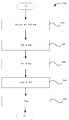
도 13 및 도 14는 계면 층들(214)의 제어 증착을 위한 공정들 1300, 1400을 설명하는 흐름도이다. 공정 1300은 금속-리치 변화 층(210)을 생성하기 위해 도입도는 산소의 양을 감소하고 변화 층(210)에서 결함들의 양을 증가시키는 ALD 공정을 사용하는 변화 층(210)의 증착을 설명한다. 부가적으로, 공정 1300은 계면 층(214)의 원하는 두께를 얻기 위해 프로세싱 파라메터들을 선택함으로써 계면 층(214)의 사이즈를 조정하기 위해 사용될 수 있다. 공정 1400은 계면 층(214)을 충분히 감소 또는 제거하는 실리사이드 전극(206)의 증착을 설명한다.13 and 14 are
원자 층 증착(atomic layer deposition)(ALD)은 다양한 반도체 프로세싱 동작 동안에 원자 스케일(scale) 두께 제어로 등각 층들(conformal layers)을 증착하기 위해 사용된 공정이다. 금속 산화물을 증착하기 위해, ALD는 두 개의 시약들(reagents), 즉 금속 전구체(precursor) 및 산소 소스(source)(예를 들어, 산화제(oxidant))를 포함하는 다중-단계(multi-step) 자기-제한(self-limiting) 공정이다. 일반적으로, 제 1 시약은 기판을 포함하는 프로세싱 챔버안으로 도입되어 기판의 표면상에 흡착된다. 초과 제 1 시약은 정화 및/또는 멀리 펌핑된다. 그 다음 제 2 시약은 챔버 내로 도입되어 증착 반응을 거쳐서 증착 층을 형성하기 위해 흡착 층(adsorbed layer)과 반응한다. 증착 반응은 일단 초기에 흡착 층이 제 2 시약과 반응하여 소비되자마자 반응이 종료되는 자기-제한이다. 초과 제 2 시약은 정화 및/또는 멀리 펌핑된다. 상술한 단계들은 하나의 증착 또는 ALD "사이클(cycle)"을 구성한다. 이 공정은 다음 층을 형성하기 위해 반복되고, 다수의 사이클들은 전체 증착된 필름 두께를 결정한다.Atomic layer deposition (ALD) is a process used to deposit conformal layers with atomic scale thickness control during various semiconductor processing operations. To deposit metal oxides, the ALD is a multi-step comprising two reagents, a metal precursor and an oxygen source (eg, an oxidant). It is a self-limiting process. Generally, the first reagent is introduced into a processing chamber containing the substrate and adsorbed onto the surface of the substrate. Excess first reagent is purged and / or pumped away. The second reagent is then introduced into the chamber and reacts with an adsorbed layer to form a deposition layer via a deposition reaction. The deposition reaction is a self-limitation in which the reaction ends once the adsorption layer is initially consumed by the second reagent and consumed. Excess second reagent is purged and / or pumped away. The above steps constitute one deposition or ALD "cycle". This process is repeated to form the next layer, and multiple cycles determine the total deposited film thickness.
도 13을 참조하면, 공정 1300은 동작 1302에서 기판 상에 하부 전극을 증착하기 시작한다. 하부 전극(예를 들어, 전극(206))은 상술한 전극 재료들 중 하나 일 수 있고, 그러나 일 실시예에서 하부 전극은 변화 층(210)의 증착 동안에 실리콘 산화물 계면 층(214)을 형성할 수 있는 폴리실리콘 전극이다. 다른 실시예들에서, 하부 전극은 변화 층(210)의 증착 동안에 또한 산화될 수 있는 금속 전극이다.Referring to FIG. 13,
동작 1304에서, 얇은 PVD 금속 산화물 층은 기판 상에 임의로 증착된다. 얇은 PVD 금속 산화물 층은 PVD 증착 공정이 계면 층(214)의 성장(도 5 참조)을 촉진하지 않는 것을 도시하므로 계면 층(214)은 제거하기 위해 사용할 수 있다. 일단 얇은(예를 들면, <10Å) PVD 금속 산화물 층이 증착되자마자, 동작 1306에서 ALD 공정이 수행될 수 있다.In
동작 1306에서, 변화 층(210)은 ALD를 사용하여 증착된다. 동작 1304는 ALD 공정의 여러 사이클들을 설명하는 여러 컴포넌트(compinent) 동작들(1308-1320)을 포함한다. 이들 동작들 중 일부는 임의적이거나, 또는 서로 다른 순서로 완료될 것이다.In
동작 1308에서, ALD 공정의 증착 온도는 임의로 낮게 된다. 증착 온도는 예를 들어, 가열된 기판 받침대(pedestal)의 온도(즉, 받침대 온도)를 저하시킴으로써 낮아질 수 있다. 몇몇 실시예들에서, 증착 온도 또는 받침대 온도는 250℃ 이하, 200℃ 이하, 175℃ 이하 등일 수 있다. 보다 낮은 온도는 산화 동안에 표면 종들의 평형 전환(equilibrium conversion)을 변경할 수 있고, 변화 층(210)에서 전기적 결함들의 농도를 바꾼다. 부가적으로, 감소된 증착 온도는 열 산화 비율을 감소시킴으로써 계면 층(214)을 감소 또는 제거할 수 있다. 예를 들면, 실리콘 전극(206)을 사용하면, ALD 증착 온도를 200℃ 이하로 감소시키는 것은 임의의 계면 층(214)을 실질적으로 감소시킬 수 있다.In
동작 1310에서, 전구체 소스(source)는 원하는 압력으로 유지된다. 원하는 증기 압력은 전구체 소스의 온도를 제어함으로써 달성될 수 있다. 전구체 소스는 ALD 증착 챔버 외부에 있고, 따라서 증착 챔버의 온도와는 다른 온도로 유지될 수 있다. 원하는 온도와 압력은 사용되는 전구체에 따른다. 예를 들면, 하프늄 산화물을 증착하기 위해 테트라키스(tetrakis)(디메틀야미노; dimethlyamino) 하프늄(TDMAH)을 사용하면, 전구체 소스는 30-100℃, 또는 40-50℃로 유지될 수 있다. 몇몇 실시예들에서, 전구체 소스의 온도는 전구체의 부분 압력을 증가시키기 위해 증가될 수 있고, 이는 또한 챔버에서 금속 전구체의 농도를 증가시킴으로써 많은 금속-리치 변화 층을 생성할 수 있다. 동작 1312에서, 전구체는 ALD 공정을 시작하기 위해 하부 전극을 포함하는 기판에 도입된다.In
동작 1314 및 1316은 금속 산화물을 형성하기 위해 사용되는 산소 소스의 처리를 설명한다. 메모리 소자(102)의 특징들에 따라, 동작들 1314 및 1316 중 하나 또는 양자는 계면 층(214)의 두께를 제어하기 위해 사용될 수 있다. 산소 소스는 오존(ozone), 산소, 수증기(water vapor), 이소프로필 알콜(IPA)(isopropyl alcohol), 에탄올 또는 다른 알콜, 또는 다른 ALD 산소 소스일 수 있다. 몇몇 형상들을 위해, ALD 공정에서 산소 소스로서 수증기를 사용하는 것은 개선된 변화 특징들을 갖는 메모리 소자들로 초래된다.
동작 1314에서, 산소 소스가 물 또는 이소프로필 알콜과 같은 액체 또는 고체인 경우, 이는 저(less) 산소를 갖는 변화 층(210)을 생성하기 위해 대표적인 것 보다 낮은 증기압으로 유지된다. 산화제의 부분 압력은 그 증기 압력을 감소시키는 소스 온도를 감소시킴으로써 감소될 수 있다. 부분 압력은 아르곤과 같은 불활성 가스를 갖는 산화제를 희석시킴으로써 또한 감소될 수 있다. 산소 및 오존과 같은 몇몇 산화제들은 그들 소스들에 있는 가스들이고, 따라서 그들 부분적 압력은 소스 온도를 변경함으로써 조작할 수 없다. 산화 정도를 감소시키는 제 3 방법은 산화제 자체의 선택을 통한다. 예를 들면, 오존과 산소는 더 많이 산화되는 경향이 있는(즉, 많은 산소를 갖는 층을 더 빨라 생성) 반면에, 수증기는 덜 산화되고, IPA 및 에탄올은 여전히 덜 산화된다. 챔버에서 산소 소스의 양을 제한하는 것은 필름을 자기-제한되게 하는 한편, 필름에서 산소의 양을 감소시킨다. 금속 원자들에 부착되는 비반응성 리간드들(unreacted ligand)은 후-증착(post-deposition) 처리를 통해 부분적으로 또는 거의 완전히 제거될 수 있다. 산소 부족(deficient) 필름은 그런 다음 메모리 소자(102)의 변화를 제어하기 위해 사용될 수 있는 결함들인 산소 공극들을 가질 수 있다.In
예를 들어, 금속-리치 하프늄 산화물 변화 층(210)을 증착하기 위해, 수증기는 산소 소스로서 사용될 수 있고, 수증기 소스는 0 내지 10℃와 같은 감소된 온도로 유지될 수 있다. 감소된 온도는 산소 소스의 증기 압력을 감소하여, ALD 사이클 당 산화의 양을 효과적으로 감소시킨다. 이러한 기술을 사용하여 형성된 하프늄 산화물 필름들은 HfO1 .2 내지 HfO1 .9, 또는 HfO1 .7의 원소 조성들(elemental compositions)로 초래될 수 있다. 일반적으로, 산소 농도들(concentrations)은 화학양론(stoichiometric) 조성들의 60-95%로 감소될 수 있다(즉, 산소의 양이 화학양론 금속 산화물, 예를 들어 HfO1 .2 내지 HfO1 .9의 60-95% 사이에 있다). IPA 또는 에탄올은 산소를 제공하기 위해 사용될 수 있으나, 동일 온도에서 상술한 수증기 또는 다른 산소 소스들보다 적은 산소를 제공할 수 있다. 따라서, IPA 또는 에탄올은, 비록 유사한 온도 감소가 변화 층(210)에서 산소의 양을 감소시키기 위해 IPA 또는 에탄올과 함께 또한 사용될 수 있을 지라도, 실온 소스를 사용하는 금속-리치 필름들을 증착할 수 있다.For example, to deposit the metal-rich hafnium
동작 1318에서, 산소 소스는 금속 산화물의 ALD 층을 생성하기 위해 기판에 도입된다. 단일 ALD 사이클은 예를 들어, 0.5Å의 두께를 갖는 필름을 증착할 수 있고, 다중 사이클들은 원하는 두께의 변화 층(210)을 통상적으로 형성할 필요가 있다. 동작 1320에서, 많은 사이클들이 필요하다면, 공정 1300은 동작 1322로 진행한다.In
동작 1322에서, 커플링 층이 증착된다. 커플링 층(212)은 얇은 층, 예를 들어 변화 층의 두께보다 25%작은 얇은 층일 수 있다. 커플링 층(212)은 ALD, PVD 등과 같은 임의의 증착 방법을 사용하여 증착될 수 있다. 동작 1324에서, 상부 전극(예를 들어, 전극(208))이 증착된다.In
동작 1326에서, 메모리 소자가 어닐된다. 어닐링은 ALD 공정의 저 증착 온도 때문에 필름에 존재할 수 있는 비반응성 전구체 리간드들을 제거할 수 있다. 일 예로, 소자는, 비록 진공 어닐들, 산화 어닐들 등과 같은 다른 어닐드이 사용될 수 있을지라도, 수소/아르곤 혼합물(예를 들어, 2-10% 수소, 90-98% 아르곤)을 사용하여 어닐된다.In
도 14로 돌아가서, 공정 1400은 메모리 소자들(102)에서 사용하기 위한 하부 전극(206)의 형성을 설명한다. 공정 1400은 그렇게 원한다면, 계면 층(214)을 제거하기 위해 사용될 수 있는 실리사이드 전극의 증착을 설명한다. 몇몇 실시예들에서, 실리사이드 증착은 변화 층(210)의 증착 동안에 계면 층(214)을 형성하지 않는다. 공정 1400은 몇몇 실시예들에서 공정 1300과 관련하여 사용될 수 있다. 예를 들면, 공정 1400의 동작들(1402-1412)은 공정 1300의 동작(1302)으로 대체될 수 있다.Returning to FIG. 14,
동작 1402에서, 하부 전극(예를 들어, 전극(206))은 기판 상에 증착된다. 하부 전극은 금속 실리사이드, 예를 들어 티타늄, 코발트, 니켈, 팔라듐, 또는 백금 실리사이드이고, 동작 1404-1412에 따라 증착된다.In
동작 1404에서, 실리콘은 기판 상에 증착된다. 동작 1406에서, 티타늄, 코발트, 니켈, 몰리브덴, 팔라듐, 또는 백금과 같은 금속은 실리콘 상에 증착된다. 동작 1408에서, 열 처리는 실리콘을 금속 안으로 상호확산(interdiffusing)시킴으로써 실리사이드 층을 형성하기 위해 수행된다. 동작 1410에서, 임의의 비반응성 금속은 전극으로부터 스트립되고(stripped), 동작 1412에서 전극은 전극의 저항성을 저하하기 위해 임의로 어닐될 수 있다.In
실리사이드 전극이 증착된 후에, 동작 1414에서 변화 층은 전극 상에 증착되고(예를 들어, 공정 1300에서 설명된 기술을 사용하여), 동작 1416에서 상부 전극(예를 들어, 전극(208))은 변화 층 위에 증착된다. 실리사이드 전극은 산화물 층의 형성에 저항하고, 따라서 계면 층(214)을 형성하지 않는다. 비록 일부 실시예들에서 계면 층(214)을 유지하는 것이 바람직할지라도, 다른 예들에서 이는 계면 층(214)을 제거하는 것이 더 바람직하고, 공정 1400은 그렇게 행하기 위한 대안적인 기술이다.After the silicide electrode is deposited, in
도 15는 다양한 실시예들에 따라 메모리 소자를 형성하기 위한 공정 1500을 설명하는 흐름도이다. 공정 1500은 그렇게 원한다면 동작 1300에서 설명한 공정과 조합하여 사용될 수 있다.15 is a flowchart illustrating a
동작 1502에서, 하부 전극은 기판 상에 증착된다. 하부 전극은 예를 들어 본 명세서에 기재된 n-형 폴리실리콘 또는 다른 물질들일 수 있다. 동작 1504에서, 변화 층(210)은 하부 전극 상에 증착된다. 변화 층(210)은 상술한 물질들 중 임의의 것, 예를 들어 HfOX, CuOX, ZnOX, CeOX 등일 수 있다. 변화 층(210)은 ALD 또는 PEALD와 같은 적합한 증착 기술들을 사용하여 증착될 수 있다.In
동작 1506에서, 변화 층(210)은 임의적으로 도핑된다. 예를 들면, 변화 층(210)은 p-형 변화 층(예를 들어, p-형 ZnOX 또는 CuOX 층)을 생성하기 위해 도핑될 수 있다. 동작 1508에서, 금속성 또는 부분적으로 금속성(예를 들어 Ti 또는 Ti/TiOX) 또는 금속 산화물(예를 들어, ZrO2, Al2O3)과 같은 커플링 층은 변화 층 상에 증착된다.In
동작 1210에서, 메모리 소자는 예를 들어, 급속 열 산화(RTO)(rapid thermal oxidation), 수소/아르곤 혼합물, 진공 어닐 등을 사용하여 어닐된다. 어닐링은 몇몇 실시예들에서 금속 산화물 변화 층(210)으로부터 커플링 층(212)으로 산소를 이동하게 한다(도 2b 참조).
In
Ⅵ. 대표적 데이터(VI. Representative data ( RepresentativeRepresentative DataData ))
A. 변화 특징들(A. Change Features SwitchingSwitching CharacteristicsCharacteristics ))
표 3은 본 명세서에 기재된 실시예들을 사용하여 형성된 메모리 소자들, 및 비교로서 다른 메모리 소자들을 위한 다양한 변화 매트릭스들(metrics)을 포함한다.Table 3 includes memory elements formed using the embodiments described herein, and various change matrices for other memory elements as a comparison.
HfOX/TiO2는 n-형 폴리실리콘 전극(206), 250℃로 증착된 50Å 두꺼운 하프HfO X / TiO 2 is an n-
늄 산화물 변화 층(210), 250℃로 증착된 8Å 티타늄 산화물 커플링 층
(212), 및 티타늄 질화물 전극(208)을 포함하는 메모리 소자로 언급된다.212, and a
HfOX/Al2O3은 n-형 폴리실리콘 전극(206), 250℃로 증착된 50Å 두꺼운 하프HfO X / Al 2 O 3 is an n-
늄 산화물 변화 층(210), 250℃로 증착된 8Å 알루미늄 산화물 커플링 층
(212), 및 티타늄 질화물 전극(208)을 포함하는 메모리 소자로 언급된다.212, and a
HfOX/ZrO2는 n-형 폴리실리콘 전극(206), 250℃로 증착된 50Å 두꺼운 하프HfO X / ZrO 2 is an n-
늄 산화물 변화 층(210), 250℃로 증착된 8Å 지르코늄 산화물 커플링 층
(212), 및 티타늄 질화물 전극(208)을 포함하는 메모리 소자로 언급된다.212, and a
HfAlXOY는 n-형 폴리실리콘 전극(206), 250℃로 증착된 58Å 알루미늄-도핑HfAl X O Y is an n-
된 하프늄 산화물 커플링 층(212), 및 티타늄 질화물 전극(208)을 포함하는Hafnium
메모리 소자로 언급된다.It is referred to as a memory element.
모든 데이터는 바이폴리 변화에 대한 것이고, 양산율(yield)은 신뢰성 있게 변화하는 메모리 소자들의 주어진 샘플에서의 비율로 언급된다. 전극(208)은 접지되고, 펄스들은 전극(206)에 인가된다. 도시된 바와 같이, HfOX/Al2O3 및 HfOX/ZrO2 메모리 소자들에서 보다 높은 밴드갭 커플링 층들은 개선된 형성 또는 재설정 전압들 및 개선된 사이클링 양산율들을 도시한다.All data are for bipoly changes and yield is referred to as the ratio in a given sample of memory elements that change reliably.
HfAlXOY 및 HfOX/Al2O3 메모리 소자들은 동일한 두께와 동일한 물질 조성들을 갖는다. 그러나, HfAlXOY 메모리 소자는 알루미늄-도핑되고, 하프늄 산화물 층 전반에 걸쳐 분산된 알루미늄을 갖는 반면에, HfOX/Al2O3 메모리 소자는 벌크 하프늄 산화물 층 및 작은 알루미늄 산화물 커플링 층을 갖는다. HfOX/Al2O3을 위한 변화 특징들은 더 양호하고, 개선된 변화는 커플링 층(212)과 변화 층(210) 사이의 계면에 형성된 결함들일 수 있는 것을 제시한다.
HfAl X O Y and HfO X / Al 2 O 3 memory devices have the same thickness and the same material compositions. However, HfAl X O Y memory devices are aluminum-doped and have aluminum dispersed throughout the hafnium oxide layer, whereas HfO X / Al 2 O 3 memory devices have a bulk hafnium oxide layer and a small aluminum oxide coupling layer. Have Change characteristics for HfO X / Al 2 O 3 are better, suggesting that the improved change may be defects formed at the interface between the
B. 계면 층(B. interfacial layer ( InterfaceInterface LayerLayer ))
공정 1300에 기재된 기술들은 계면 층(214)을 실질적으로 제거하는 메모리 소자(102)를 증착하기 위해 사용된다. 알루미늄 산화물은 트리메틸알루미늄(trimethylaluminum) 및 수증기를 사용하여 증착된다. 가스 상(gas phase)에서 수증기의 양은 수증기 소스의 온도를 1-5°로 저하시킴으로써 제한된다. 이러한 기술을 사용하여, 계면 층(214)의 두께는 1.1nm(수증기가 실온에 유지되는 경우)로부터 대략 제로(0)로 감소된다. 몇몇 실시예들에서, 계면 층(214)의 제거는 형성 전압을 감소할 것이다.
The techniques described in
C. 극성 및 변화 양산율(C. Polarity and mass change rate PolarityPolarity andand SwitchingSwitching YieldYield ))
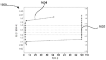
도 16a는 낮은 일 함수(work funcion) 전극이 음(nagative)의 전압 설정 펄스 및 양(positive)의 전압 재설정 펄스를 수신할 때에 높은 사이클링 양산율(yield)을 도시하는 그래프(1600)이다. 메모리 소자 형성은 n-형 폴리실리콘 전극(206), 원자 층 증착(ALD)-증착된 하프늄 산화물 변화 층(210), ALD-증착된 티타늄 산화물 커플링 층(212) 및 물리적 기상 증착(PVD)-증착된 티타늄 질화물 전극(208)을 포함한다. 플로트(plot)(1602)는 보다 낮은 일 함수 전극(여기선 n-형 폴리실리콘 전극)이 공통 전기적 기준에 대해 음의 전압 설정 펄스 및 양의 전압 재설정 펄스를 수신하는 메모리 소자들을 반영한다. 공통 전기적 기준은 접지, +2V 등과 같은 임의의 전압일 수 있다. 전극은 전압이 전극에서 가시적이라면 전압을 수신하는 것이라고 말하고; 예를 들어 폴리실리콘 전극(206)은 전압 펄스가 다른 곳에서 배향되는 경우에도 양의 재설정 전압을 보일 수 있다.FIG. 16A is a
폴로트(1602)에서 볼 수 있는 바와 같이, 보다 낮은 일 함수 전극이 음의 전압 설정 펄스를 수신하는 메모리 소자들의 대략 85%는 100 사이클을 지난다. 대조적으로, 플로트(1604)는 보다 낮은 일 함수 전극이 양의 전압 설정 펄스 및 음의 전압 재설정 펄스를 수신하는 메모리 소자들을 반영한다. 볼 수 있는 바와 같이, 메모리 소자들 중 어느 것도 60 사이클을 지나 잔존하지 않고, 10 사이클까지 매우 작은 수가 잔존한다. 그런 다음 본 명세서에 기재된 메모리 소자들을 사용하면, 보다 낮은 일 함수 전극은 음의 전압 설정 펄스 및 양의 전압 재설정 펄스를 수신해야 하는 것을 추축할 수 있다.As can be seen in
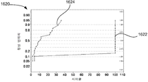
도 16b는 두 전극들이 0.1 eV 및 1.0 eV 사이에서 다른 일 함수를 갖는 경우에 높은 사이클링 양산율을 도시하는 그래프(1620)이다. 0.1 eV 보다 높으나 1.0 eV 보다 작은 만큼 다른 일 함수를 갖는 전극들(206, 208)을 포함하는 메모리 소자들은 1.0 eV 보다 많은 만큼 다른 일 함수를 갖는 전극들을 포함하는 메모리 소자들과 비교하여 높은 사이클링 양산율을 나타낸다. 그래프(1620)는 플로트들(1622, 1624)에 의해 나타나는 두 개의 메모리 소자 형상들을 위한 사이클링 양산율을 도시한다. 플로트(1622)로 나타나는 형상은 n-형 폴리실리콘 전극(206), 하프늄 산화물 변화 층(210), 티타늄 산화물 커플링 층(212), 및 티타늄 질화물 전극(208)을 포함한다. n-형 폴리실리콘은 대략 4.1 eV의 일 함수를 갖는 반면, 티타늄 질화물은 대략 0.4-0.5 eV의 차이를 갖는 대략 4.5-4.6 eV의 일 함수를 갖는다. 플로트(524)로 나타나는 형상은 n-형 폴리실리콘 전극(402), 하프늄 산화물 변화 층(406), 티타늄 산화물 층(418), 및 백금 전극(404)을 포함한다. n-형 폴리실리콘은 대략 4.1 eV의 일 함수를 갖는 반면, 백금은 대략 1.6 eV의 차이를 갖는 대략 5.7 eV의 일 함수를 갖는다. 볼 수 있는 바와 같이, 플로트(522)는 높은 사이클링 양산율을 도시하는 반면에, 플로트(524)는 낮은 사이클링 양산율을 도시하며, 본 명세서에 기재된 메모리 소자들에 사용된 전극들을 지시하고, 이들이 1.0 eV 보다 낮은 일 함수 차이를 가질 때에 더 효과적인다.
FIG. 16B is a
D. 커플링 층의 두께 및 변화 양산율(D. Thickness and Change Mass Production of Coupling Layer ( ThickenssThickenss ofof CouplingCoupling LayerLayer andand Switching Switching YieldYield ))
사이클링 양산율은 보다 높은 밴드갭 물질(즉, 4 eV 보다 큰 밴드갭을 갖는 물질들)과 커플링 층의 증가된 두께를 개선하기 위해 도시될 수 있다. 표 4는 보다 낮은 일 함수 전극이 설정 펄스 동안에 양가인 경우에 바이폴라 변화를 사용하여 평가되는 몇몇 메모리 소자들을 위한 사이클링 양산율을 나타낸다. 각 형상에 대해, 18 소자들이 시험되었고, 각 메모리 소자는 금속 산화물 변화 층 아래의 n-형 폴리실리콘 전극과 커플링 층 위의 티타늄 질화물 전극을 포함한다. 도시된 바와 같이, 가장 높은 사이클링 양산율은 비록 다른 조합들(예를 들면, 70Å 하프늄 산화물 층)이 수용가능한 결과를 또한 도시할지라도, 50Å 두꺼운 하프늄 산화물 층과 5Å 두꺼운 티타늄 산화물 층을 포함하는 메모리 소자들을 위한 것이다.Cycling yield can be shown to improve the increased thickness of the coupling layer with higher bandgap material (ie, materials with a bandgap greater than 4 eV). Table 4 shows the cycling yields for some memory devices evaluated using bipolar change when the lower work function electrode is positive during the set pulse. For each shape, 18 devices were tested, each memory device comprising an n-type polysilicon electrode under the metal oxide change layer and a titanium nitride electrode over the coupling layer. As shown, the highest cycling yield yields a memory comprising a 50 Å thick hafnium oxide layer and a 5 Å thick titanium oxide layer, although other combinations (eg, 70 Å hafnium oxide layers) also show acceptable results. For the devices.
양산율cycling
Mass production rate
금속 산화물 층의 두께가 금속 산화물 층과 커플링 층의 전체 두께의 80%보다 많은 메모리 소자들은 개선된 사이클링 양산율을 도시할 수 있다. 예를 들면, 50Å 하프늄 산화물 층과 5Å티타늄 산화물 층을 포함하는 메모리 소자들은 두께에 있어서 80% 이상의 하프늄 산화물을 포함하고 높은 사이클링 양산율을 도시한다. 이와 대조하여, 30Å 하프늄 산화물 층과 5Å 티타늄 산화물 층을 포함하는 메모리 소자들은 두께에 있어서 80% 이하의 하프늄 산화물을 포함하고 낮은 변화 양산율을 도시한다. 따라서, 보다 높은 밴드갭(4 eV보다 큰) 물질들의 비율은 개선된 변화 특징들로 유도된다.Memory elements where the thickness of the metal oxide layer is greater than 80% of the total thickness of the metal oxide layer and the coupling layer may exhibit improved cycling yield. For example, memory devices comprising a 50 Å hafnium oxide layer and a 5 Å titanium oxide layer contain at least 80% hafnium oxide in thickness and exhibit high cycling yield. In contrast, memory devices comprising a 30 Å hafnium oxide layer and a 5 Å titanium oxide layer contain up to 80% hafnium oxide in thickness and show low change yield rates. Thus, the proportion of higher bandgap (greater than 4 eV) materials leads to improved change characteristics.
부가적으로, 다른 메모리 소자 디자인은 도핑된 폴리실리콘 하부 전극, 폴리실리콘 전극에 인접한 5Å 티타늄 산화물 층, 및 티타늄 산화물 층과 티타늄 질화물 상부 전극 사이의 50Å 하프늄 산화물 층을 갖는 MIS-스타일 적층체를 포함한다. 이러한 디자인은 33.3%의 사이클링 양산율(18 디바이스들 중 6개가 100 사이클에 잔존함)을 도시하고, 메모리 소자 내의 금속 산화물 층들의 배열이 디바이스 잔존에 영향을 미칠 수 있는 것을 도시한다.Additionally, other memory device designs include a MIS-style laminate having a doped polysilicon bottom electrode, a 5 Å titanium oxide layer adjacent to the polysilicon electrode, and a 50 Å hafnium oxide layer between the titanium oxide layer and the titanium nitride top electrode. do. This design shows a cycling yield of 33.3% (6 of 18 devices remain at 100 cycles) and show that the arrangement of metal oxide layers in the memory device can affect device remaining.
다른 보다 높은 밴드갭 물질들(예를 들어, TaOX, AlOX, LaOX, ZrOX, YOX)은 상기 표에서 하프늄 산화물을 대체 또는 보충할 수 있고 양호한 결과를 도시한다. 예를 들어, 하프늄 산화물 층은 알루미늄 산화물 층, 란탄(lanthanum) 산화물 층, 하프늄 산화물 층, 또는 하프늄 란탄 산화물 층으로 대체될 수 있다.
Other higher bandgap materials (eg, TaO X , AlO X , LaO X , ZrO X , YO X ) can replace or supplement hafnium oxide in the table above and show good results. For example, the hafnium oxide layer can be replaced with an aluminum oxide layer, a lanthanum oxide layer, a hafnium oxide layer, or a hafnium lanthanum oxide layer.
Ⅶ. 대표적인 실시예들(VII. Representative embodiments ( RepresentatineRepresentatine EmbodimentsEmbodiments ))
일 실시예에 따르면, 저항-변화 메모리 소자(resistive-switching memory element)가 제공되고, 이 소자는 제 1 전극 및 제 2 전극, 하프늄 산화물을 포함하고 제 1 두께를 갖는 상기 제 1 전극과 제 2 전극 사이의 변화 층(switching layer), 및 상기 변화 층과 상기 제 2 전극 사이의 커플링 층(coupling layer)으로서, 상기 커플링 층은 알루미늄 산화물 및 지르코늄 산화물로 구성되는 그룹으로부터 선택되는 물질(material)을 포함하며 제 1 두께보다 25% 작은 제 2 두께를 갖는 상기 커플링 층(coupling layer)을 포함한다.According to one embodiment, a resistive-switching memory element is provided, said element comprising a first electrode and a second electrode, hafnium oxide, said first electrode and a second having a first thickness; A switching layer between electrodes, and a coupling layer between the change layer and the second electrode, wherein the coupling layer is selected from the group consisting of aluminum oxide and zirconium oxide. And a coupling layer having a second thickness of 25% less than the first thickness.
다른 실시예에 따르면, 메모리 소자의 제 1 전극은 도핑된 실리콘이고, 메모리 소자는 제 2 전극에서 공통 전기적 기준(common electrical reference)에 대해 음(negative)의 재설정(reset) 전압과 공통 전기적 기준에 대해 양(positive)의 설정 전압을 수신하기 위해 형성된다.According to another embodiment, the first electrode of the memory element is doped silicon, and the memory element is at a negative reset voltage and a common electrical reference relative to a common electrical reference at the second electrode. To receive a positive set voltage relative to the
다른 실시예에 따르면, 메모리 소자의 제 1 전극은 제 1 물질을 포함하고, 제 2 전극은 제 2 물질을 포함하며, 제 1 물질은 제 2 물질과는 다르다.According to another embodiment, the first electrode of the memory element comprises a first material, the second electrode comprises a second material, and the first material is different from the second material.
다른 실시예에 따르면, 제 1 전극의 제 1 물질은 도핑된 실리콘이고, 제 2 전극의 제 2 물질은 티타늄 질화물이다.According to another embodiment, the first material of the first electrode is doped silicon and the second material of the second electrode is titanium nitride.
다른 실시예에 따르면, 메모리 소자의 제 1 두께는 20 및 100 옹스트롬(Å) 사이이다.According to another embodiment, the first thickness of the memory element is between 20 and 100 angstroms.
다른 실시예에 따르면, 메모리 소자의 변화 층은 HfO1 .2 및 HfO1 .7 사이의 원소 조성(elemental composition)을 갖는 하프늄 산화물 물질을 포함한다.According to another embodiment, the variable layer of the memory element comprises a hafnium oxide material having an element composition (elemental composition) of between 1 .2 and HfO HfO 1 .7.
다른 실시예에 따르면, 제 1 전극의 제 1 물질은 n-형 폴리실리콘(n-type polysilicon)이다.According to another embodiment, the first material of the first electrode is n-type polysilicon.
다른 실시예에 따르면, 메모리 소자의 제 1 전극과 제 2 전극 중 적어도 하나는 변화 층과 같은 동일한 최상의 공통 산화 상태(most common oxidation state)를 갖는다.According to another embodiment, at least one of the first and second electrodes of the memory element has the same most common oxidation state, such as a change layer.
다른 실시예에 따르면, 메모리 소자는 제 1 전극과 변화 층 사이의 계면 층을 포함하고, 이 계면 층은 10Å보다 작은 두께를 갖는다.According to another embodiment, the memory element comprises an interface layer between the first electrode and the change layer, the interface layer having a thickness of less than 10 GPa.
다른 실시예에 따르면, 메모리 소자의 계면 층은 실리콘 산화물을 포함한다.According to another embodiment, the interfacial layer of the memory device comprises silicon oxide.
다른 실시예에 따르면, 메모리 소자의 제 2 전극의 일 함수는 제 1 전극의 일 함수보다 크고, 제 1 전극은 공통 전기적 기준에 대해 음의 전압을 갖는 형성 전압 펄스(forming voltage pulse)를 수신하기 위해 형성된다.According to another embodiment, the work function of the second electrode of the memory element is greater than the work function of the first electrode, the first electrode receiving a forming voltage pulse having a negative voltage with respect to a common electrical reference. To be formed.
또 다른 실시예에 따르면, 저항-변화 메모리 소자가 제공되고, 이 소자는 제 1 전극 및 제 2 전극, 상기 제 1 전극과 제 2 전극 사이의 변화 층으로서, 상기 변화 층은 4 전자 볼트(eV)보다 큰 제 1 밴드갭을 갖는 제 1 금속 산화물을 포함하며 제 1 두께를 갖는 상기 변화 층, 및 상기 변화 층과 상기 제 2 전극 사이의 커플링 층으로서, 상기 커플링 층은 제 1 밴드갭 이상의 제 2 밴드갭을 갖는 제 2 금속 산화물을 포함하며 제 1 두께보다 25% 작은 제 2 두께를 갖는 상기 커플링 층을 포함한다.According to yet another embodiment, a resistance-change memory element is provided, which element is a change layer between a first electrode and a second electrode, said first electrode and a second electrode, said change layer being a four electron volt (eV). Said change layer comprising a first metal oxide having a first bandgap greater than) and having a first thickness, and a coupling layer between said change layer and said second electrode, wherein said coupling layer comprises a first bandgap; It includes the second metal oxide having a second bandgap of the above and includes the k-fling layer having a second thickness of 25% less than the first thickness.
다른 실시예에 따르면, 메모리 소자의 제 1 금속 산화물은 화학양론(stoichiometric)의 60 및 95% 사이의 산소 농도(concentration)를 갖는다.According to another embodiment, the first metal oxide of the memory device has an oxygen concentration between 60 and 95% of stoichiometric.
다른 실시예에 따르면, 메모리 소자의 제 1 전극은 도핑된 실리콘 및 티타늄 질화물로 구성되는 그룹으로부터 선택되고, 제 2 전극은 몰리브덴 질화물, 몰리브덴 산화물, 티타늄 질화물, 텅스텐, 탄탄륨 질화물, 몰리브덴 질화물, 몰리브덴 산화물, 백금, 루테늄, 니켈, 이리듐, 이리듐 산화물, 및 루테늄 산화물로 구성되는 그룹으로부터 선택된다.According to another embodiment, the first electrode of the memory element is selected from the group consisting of doped silicon and titanium nitride, and the second electrode is molybdenum nitride, molybdenum oxide, titanium nitride, tungsten, tantalum nitride, molybdenum nitride, molybdenum Oxide, platinum, ruthenium, nickel, iridium, iridium oxide, and ruthenium oxide.
다른 실시예에 따르면, 변화 층의 제 1 두께는 20 및 100Å 사이이다.According to another embodiment, the first thickness of the change layer is between 20 and 100 mm.
다른 실시예에 따르면, 제 1 금속 산화물의 제 1 금속은 제 2 금속 산화물의 제 2 금속의 제 2 최상의 공통 산화 상태와는 다른 제 1 최상의 공통 산화 상태를 갖는다.According to another embodiment, the first metal of the first metal oxide has a first best common oxidation state that is different from the second best common oxidation state of the second metal of the second metal oxide.
다른 실시예에 따르면, 제 1 금속 산화물의 제 1 금속과 제 2 금속 산화물의 제 2 금속은 동일한 최상의 공통 산화 상태를 갖는다.According to another embodiment, the first metal of the first metal oxide and the second metal of the second metal oxide have the same best common oxidation state.
다른 실시예에 따르면, 제 2 금속 산화물의 제 2 금속은 제 1 금속 산화물의 제 1 금속의 제 1 최상의 공통 산화 상태 이하인 제 2 최상의 공통 산화 상태를 갖는다.According to another embodiment, the second metal of the second metal oxide has a second best common oxidation state that is less than or equal to the first best common oxidation state of the first metal of the first metal oxide.
다른 실시예에 따르면, 제 1 금속 산화물은 하프늄 산화물이고, 제 2 금속 산화물은 지르코늄 산화물 및 알루미늄 산화물로 구성되는 그룹으로부터 선택된다.According to another embodiment, the first metal oxide is hafnium oxide and the second metal oxide is selected from the group consisting of zirconium oxide and aluminum oxide.
다른 실시예에 따르면, 제 1 금속 산화물은 하프늄 산화물, 탄탈륨 산화물, 알루미늄 산화물, 지르코늄 산화물, 및 이트륨 산화물로 구성되는 그룹으로부터 선택되고, 제 2 금속 산화물은 지르코늄 산화물 및 알루미늄 산화물로 구성되는 그룹으로부터 선택된다.According to another embodiment, the first metal oxide is selected from the group consisting of hafnium oxide, tantalum oxide, aluminum oxide, zirconium oxide, and yttrium oxide, and the second metal oxide is selected from the group consisting of zirconium oxide and aluminum oxide. do.
다른 실시예에 따르면, 제 1 전극은 도핑된 실리콘을 포함하고, 실리콘 산화물을 포함하고 10Å보다 작은 두께를 갖는 변화 층과 제 1 전극 사이의 계면 층을 부가로 포함한다.According to another embodiment, the first electrode comprises doped silicon and further comprises an interfacial layer between the first electrode and the change layer comprising silicon oxide and having a thickness of less than 10 GPa.
다른 실시예에 따르면, 제 1 전극은 티타늄 실리사이드, 코발트 실리사이드, 니켈 실리사이드, 팔라듐 실리사이드, 및 백금 실리사이드로 구성되는 그룹으로부터 선택되는 실리사이드(silicide)를 포함한다.According to another embodiment, the first electrode comprises a silicide selected from the group consisting of titanium silicide, cobalt silicide, nickel silicide, palladium silicide, and platinum silicide.
다른 실시예에 따르면, 메모리 소자는 3-차원 메모리 어레이의 일부이다.According to another embodiment, the memory element is part of a three-dimensional memory array.
또 다른 실시예에 따르면, 저항-변화 메모리 소자를 형성하는 방법이 제공되고, 이 방법은 기판 상에 제 1 전극을 증착하는 단계, 원자 층 증착(atomic layer deposition)(ALD)을 사용하여 제 1 전극 위에 금속 산화물 포함하는 변화 층을 증착하는 단계로서, 상기 변화 층 증착 단계는 40℃보다 높게 전구체를 유지하는 단계, 기판에 전구체를 도입하는 단계, 10℃ 보다 낮게 산소 소스를 유지하는 단계, 및 기판에 산소 소스를 도입하는 단계를 부가로 포함하는 상기 변화 층 증착 단계, 및 변화 층 위에 제 2 전극을 증착하는 단계를 포함한다.According to yet another embodiment, a method of forming a resistance-changing memory element is provided, the method comprising depositing a first electrode on a substrate, the first using atomic layer deposition (ALD) Depositing a change layer comprising a metal oxide over an electrode, wherein the change layer deposition step comprises maintaining a precursor higher than 40 ° C., introducing the precursor into a substrate, maintaining an oxygen source below 10 ° C., and And depositing a second electrode over the change layer, further comprising the step of introducing an oxygen source into the substrate.
다른 실시예에 따르면, 산소 소스는 수증기, 이소프로필 알콜(IPA), 및 에탄올 중 적어도 하나이다.According to another embodiment, the oxygen source is at least one of water vapor, isopropyl alcohol (IPA), and ethanol.
다른 실시예에 따르면, 금속 산화물은 하프늄 산화물, 탄탄륨 산화물, 알루미늄 산화물, 이트륨 산화물, 및 지르코늄 산화물로 구성되는 그룹으로부터 선택된다.According to another embodiment, the metal oxide is selected from the group consisting of hafnium oxide, tannium oxide, aluminum oxide, yttrium oxide, and zirconium oxide.
다른 실시예에 따르면, 금속 산화물은 화학양론의 60 및 95% 사이의 산소 농도를 갖는다.According to another embodiment, the metal oxide has an oxygen concentration between 60 and 95% of the stoichiometry.
다른 실시예에 따르면, 금속 산화물은 하프늄 산화물이고, HfO1 .2 및 HfO1 .7 사이의 원소 조성을 갖는다.According to another embodiment, the metal oxide is hafnium oxide, having the elemental composition of HfO between 1 .2 and HfO 1 .7.
다른 실시예에 따르면, ALD를 위한 증착 온도는 250℃보다 낮다.According to another embodiment, the deposition temperature for the ALD is lower than 250 ° C.
다른 실시예에 따르면, ALD를 위한 증착 온도는 대략 200℃이다.According to another embodiment, the deposition temperature for the ALD is approximately 200 ° C.
다른 실시예에 따르면, 상기 방법은 제 2 전극을 증착한 후에 메모리 소자를 어닐링하는 단계를 포함한다.According to another embodiment, the method includes annealing the memory device after depositing the second electrode.
다른 실시예에 따르면, 상기 방법은 물리적 기상 증착을 사용하여 제 1 전극 위에 물리적 기상 증착(physical vapor deposition)(PVD) 층을 증착하는 단계를 부가로 포함하고, 변화 층은 PVD 층 위에 증착되며, PVD 층은 변화 층과 동일한 물질을 포함한다.According to another embodiment, the method further comprises depositing a physical vapor deposition (PVD) layer over the first electrode using physical vapor deposition, wherein the change layer is deposited over the PVD layer, The PVD layer includes the same material as the change layer.
다른 실시예에 따르면, 상기 방법은 변화 층 위에 커플링 층을 증착하는 단계를 부가로 포함하고, 이 커플링 층은 변화 층의 두께보다 25% 작은 두께를 갖는다.According to another embodiment, the method further comprises depositing a coupling layer over the change layer, the coupling layer having a thickness of 25% less than the thickness of the change layer.
다른 실시예에 따르면, 커플링 층의 밴드갭은 변화 층의 밴드갭보다 크다.According to another embodiment, the bandgap of the coupling layer is greater than the bandgap of the change layer.
다른 실시예에 따르면, 커플링 층은 알루미늄 산화물 및 지르코늄 산화물로 구성되는 그룹으로부터 선택된다.According to another embodiment, the coupling layer is selected from the group consisting of aluminum oxide and zirconium oxide.
또 다른 실시예에 따르면, 저항-변화 메모리 소자를 형성하는 방법이 제공되고, 이 방법은 기판 상에 제 1 전극을 증착하는 단계, 제 1 전극 위에 변화 층을 증착하는 단계로서, 상기 변화 층은 4 전자 볼트(eV)보다 큰 제 1 밴드갭과 제 1 두께를 갖는, 상기 변화 층 증착 단계, 변화 층 위에 커플링 층을 증착하는 단계로서, 상기 커플링 층은 제 1 두께보다 25% 작은 제 2 두께와 제 1 밴드갭 이상의 제 2 밴드갭을 갖는, 상기 커플링 층 증착 단계, 및 커플링 층 위에 제 2 전극을 증착하는 단계를 포함한다.According to another embodiment, a method of forming a resistance-changing memory element is provided, the method comprising depositing a first electrode on a substrate, depositing a change layer on the first electrode, wherein the change layer Depositing a coupling layer over the change layer, the change layer deposition step having a first bandgap and a first thickness greater than 4 electron volts (eV), the coupling layer being 25% less than the first thickness. Depositing the coupling layer, having a second thickness and a second bandgap of at least a first bandgap, and depositing a second electrode over the coupling layer.
다른 실시예에 따르면, 제 1 전극은 도핑된 실리콘이고, 변화 층을 증착하는 단계는 제 1 전극과 변화 층 사이의 실리콘 산화물을 포함하는 계면 층을 형성하는 단계를 포함하고, 계면 층은 10Å보다 작은 두께를 갖는다.According to another embodiment, the first electrode is doped silicon, and depositing the change layer comprises forming an interface layer comprising silicon oxide between the first electrode and the change layer, wherein the interface layer is less than 10 microseconds. Have a small thickness.
다른 실시예에 따르면, 변화 층은 하프늄 산화물, 탄탈륨 산화물, 알루미늄 산화물, 이트륨 산화물, 및 지르코늄 산화물로 구성되는 그룹으로부터 선택된다.According to another embodiment, the change layer is selected from the group consisting of hafnium oxide, tantalum oxide, aluminum oxide, yttrium oxide, and zirconium oxide.
다른 실시예에 따르면, 커플링 층은 지르코늄 산화물과 알루미늄 산화물로 구성되는 그룹으로부터 선택된다.According to another embodiment, the coupling layer is selected from the group consisting of zirconium oxide and aluminum oxide.
다른 실시예에 따르면, 변화 층을 증착하는 단계는 원자 층 증착(ALD)을 사용하여, 40℃보다 높게 전구체를 유지하는 단계, 기판에 전구체를 도입하는 단계, 10℃보다 낮게 산소 소스를 유지하는 단계, 및 기판에 산소 소스를 도입하는 단계를 포함한다.According to another embodiment, depositing the change layer comprises using atomic layer deposition (ALD) to maintain the precursor above 40 ° C., introducing the precursor into the substrate, maintaining the oxygen source below 10 ° C. And introducing an oxygen source to the substrate.
다른 실시예에 따르면, 변화 층을 증착하는 단계는 화학양론의 60 및 95% 사이의 산소 농도를 갖는 금속 산화물을 증착하는 단계를 포함한다.According to another embodiment, depositing the change layer includes depositing a metal oxide having an oxygen concentration between 60 and 95% of stoichiometry.
다른 실시예에 따르면, 상기 방법은 메모리 소자를 어닐링하는 단계를 포함한다.According to another embodiment, the method includes annealing the memory device.
다른 실시예에 따르면, 산소 소스는 수증기, 이소프로필 알콜, 및 에탄올 중 적어도 하나이다.According to another embodiment, the oxygen source is at least one of water vapor, isopropyl alcohol, and ethanol.
또 다른 실시예에 따르면, 저항-변화 메모리 소자가 제공되고, 이 소자는 제 1 전극 및 제 2 전극, 하프늄 산화물을 포함하고 제 1 두께를 갖는 제 1 전극과 제 2 전극 사이의 변화 층, 및 변화 층과 제 2 전극 사이의 커플링 층으로서, 상기 커플링 층은 부분적으로 금속 티타늄 및 부분적으로 티타늄 산화물을 구비하는 물질을 포함하며 제 1 두께보다 25% 작은 제 2 두께를 갖는 상기 커플링 층을 포함한다.According to yet another embodiment, there is provided a resistance-changing memory element, the element comprising a first electrode and a second electrode, a change layer between the first electrode and the second electrode comprising hafnium oxide and having a first thickness, and A coupling layer between the change layer and the second electrode, the coupling layer comprising a material comprising partially metal titanium and partially titanium oxide and having a second thickness 25% less than the first thickness It includes.
다른 실시예에 따르면, 제 1 전극은 도핑된 실리콘이고, 메모리 소자는 제 2 전극에서 공통 전기적 기준에 대해 음의 재설정 전압과 공통 전기적 기준에 대해 양의 설정 전압을 수신하기 위해 형성된다.According to another embodiment, the first electrode is doped silicon and a memory element is formed at the second electrode to receive a negative reset voltage for the common electrical reference and a positive set voltage for the common electrical reference.
다른 실시예에 따르면, 제 1 두께는 20 및 100Å 사이이다.According to another embodiment, the first thickness is between 20 and 100
다른 실시예에 따르면, 변화 층은 HfO1 .2 및 HfO1 .7 사이의 원소 조성을 갖는 하프늄 산화물 물질을 포함한다.According to another embodiment, the change layer comprises hafnium oxide material having an element composition of HfO between 1 .2 and HfO 1 .7.
다른 실시예에 따르면, 제 1 물질은 n-형 폴리실리콘이다.According to another embodiment, the first material is n-type polysilicon.
다른 실시예에 따르면, 메모리 소자는 제 1 전극과 변화 층 사이의 계면 층을 포함하고, 계면 층은 10Å보다 작은 두께를 갖는다.According to another embodiment, the memory element comprises an interface layer between the first electrode and the change layer, wherein the interface layer has a thickness of less than 10 ns.
다른 실시예에 따르면, 제 1 금속 산화물은 화학양론의 60 및 95% 사이의 산소 농도를 갖는다.According to another embodiment, the first metal oxide has an oxygen concentration between 60 and 95% of the stoichiometry.
다른 실시예에 따르면, 제 1 전극은 도핑된 실리콘 및 티타늄 질화물로 구성되는 그룹으로부터 선택되고, 제 2 전극은 몰리브덴 질화물, 몰리브덴 산화물, 티타늄 질화물, 텅스텐, 탄탄륨 질화물, 몰리브덴 질화물, 몰리브덴 산화물, 백금, 루테늄, 니켈, 이리듐, 이리듐 산화물, 티타늄/알루미늄 합금, 및 루테늄 산화물로 구성되는 그룹으로부터 선택된다.According to another embodiment, the first electrode is selected from the group consisting of doped silicon and titanium nitride, and the second electrode is molybdenum nitride, molybdenum oxide, titanium nitride, tungsten, tantalum nitride, molybdenum nitride, molybdenum oxide, platinum , Ruthenium, nickel, iridium, iridium oxide, titanium / aluminum alloy, and ruthenium oxide.
다른 실시예에 따르면, 제 1 전극은 도핑된 실리콘이고, 실리콘 산화물을 포함하고 10Å보다 작은 두께를 갖는 변화 층과 제 1 전극 사이의 계면 층을 부가로 포함한다.According to another embodiment, the first electrode is doped silicon and further comprises an interfacial layer between the first electrode and the change layer comprising silicon oxide and having a thickness of less than 10 GPa.
또 다른 실시예에 따르면, 저항-변화 메모리 소자가 제공되고, 이 소자는 도핑된 실리콘을 포함하는 제 1 전극, 전이 금속(transition metal), 전이 금속 합금, 전이 금속 질화물, 및 전이 금속 카바이드로 구성되는 그룹으로부터 선택되는 물질을 포함하는 제 2 전극, 제 1 전극과 제 2 전극 사이에 있고 하프늄 산화물, 지르코늄 산화물, 티타늄 산화물, 세륨 산화물, 아연 산화물, 란탄 산화물, 및 구리 산화물로 구성되는 그룹으로부터 선택되는 금속 산화물을 포함하는 변화 층, 및 저항-변화 금속 산화물과 제 2 전극 사이의 커플링 층을 포함하고, 커플링 층은 티타늄 금속을 적어도 부분적으로 포함한다.According to yet another embodiment, a resistive-change memory device is provided, the device comprising a first electrode comprising a doped silicon, a transition metal, a transition metal alloy, a transition metal nitride, and a transition metal carbide A second electrode comprising a material selected from the group consisting of: hafnium oxide, zirconium oxide, titanium oxide, cerium oxide, zinc oxide, lanthanum oxide, and copper oxide, between the first electrode and the second electrode; And a coupling layer between the resistive-change metal oxide and the second electrode, the coupling layer at least partially comprising titanium metal.
다른 실시예에 따르면, 커플링 층은 티타늄 금속을 실질적으로 포함하는 제 1 부분과, 티타늄 산화물을 실질적으로 포함하는 제 2 부분을 포함한다.According to another embodiment, the coupling layer comprises a first portion substantially comprising titanium metal and a second portion substantially comprising titanium oxide.
다른 실시예에 따르면, 커플링 층의 제 2 부분은 변화 층과 접촉하고, 변화 층은 산소-결함 금속 산화물을 포함하는 커플링 층의 제 2 부분과 접촉하는 제 1 부분과, 변화 층의 제 1 부분보다 더 많은 산소 농도를 갖는 금속 산화물을 포함하는 제 2 부분을 포함한다.According to another embodiment, the second portion of the coupling layer is in contact with the change layer, the change layer is in contact with the second portion of the coupling layer comprising an oxygen-deficient metal oxide and the first portion of the change layer. And a second portion comprising a metal oxide having an oxygen concentration greater than one portion.
또 다른 실시예에 따르면, 저항-변화 메모리 소자를 형성하는 방법이 제공되고, 이 방법은 기판 상에 제 1 전극을 증착하는 단계, 제 1 전극 상에 금속 산화물을 포함하는 변화 층을 증착하는 단계, 변화 층 상에 티타늄 금속을 포함하는 커플링 층을 증착하는 단계, 커플링 층 상에 제 2 전극을 증착하는 단계, 메모리 소자를 어닐링하는 단계 및 티타늄 산화물을 형성하기 위해 커플링 층의 적어도 일 부분과 산소 결함을 갖는 변화 층의 적어도 일 부분을 야기하는 단계를 포함한다.According to yet another embodiment, a method of forming a resistance-changing memory device is provided, the method comprising depositing a first electrode on a substrate and depositing a change layer comprising a metal oxide on the first electrode Depositing a coupling layer comprising titanium metal on the change layer, depositing a second electrode on the coupling layer, annealing the memory device, and at least one of the coupling layer to form titanium oxide. Causing at least a portion of the change layer with portions and oxygen defects.
다른 실시예에 따르면, 변화 층은 세륨 산화물, 하프늄 산화물, 알루미늄 산화물, 탄탈륨 산화물, 이트륨 산화물, 및 지르코늄 산화물로 구성되는 그룹으로부터 선택되는 금속 산화물이다.According to another embodiment, the change layer is a metal oxide selected from the group consisting of cerium oxide, hafnium oxide, aluminum oxide, tantalum oxide, yttrium oxide, and zirconium oxide.
다른 실시예에 따르면, 변화 층은 p-형 아연 산화물 및 p-형 구리 산화물로 구성되는 그룹으로부터 선택되는 금속 산화물이다.According to another embodiment, the change layer is a metal oxide selected from the group consisting of p-type zinc oxide and p-type copper oxide.
다른 실시예에 따르면, 상기 방법은 제 1 전극 상에 변화 층을 증착하는 단계와, p-형 금속 산화물 변화 층을 형성하기 위해 변화 층을 도핑하는 단계를 부가로 포함한다.According to another embodiment, the method further comprises depositing a change layer on the first electrode and doping the change layer to form a p-type metal oxide change layer.
다른 실시예에 따르면, 변화 층을 도핑하는 단계는 원자 층 증착(ALD) 및 플라즈마 강화 ALD(PEALD) 중 적어도 하나를 사용하는 단계를 포함한다.According to another embodiment, the doping of the change layer comprises using at least one of atomic layer deposition (ALD) and plasma enhanced ALD (PEALD).
다른 실시예에 따르면, 변화 층을 증착하는 단계는 수증기, 이소프로필 알콜(IPA), 및 에탄올 중 적어도 하나인 산소 소스를 사용하는 단계를 포함한다.According to another embodiment, depositing the change layer includes using an oxygen source that is at least one of water vapor, isopropyl alcohol (IPA), and ethanol.
다른 실시예에 따르면, ALD를 위한 증착 온도는 250℃ 보다 낮다.According to another embodiment, the deposition temperature for the ALD is lower than 250 ° C.
다른 실시예에 따르면, 상기 방법은 변화 층의 두께보다 25% 작은 두께를 갖는 커플링 층을 증착하는 단계를 포함한다.According to another embodiment, the method includes depositing a coupling layer having a thickness of 25% less than the thickness of the change layer.
비록 상술한 설명이 이해의 명확성의 목적을 위해 일부 상세하게 설명되었을지라도, 본 발명은 제공된 상세한 설명에 제한되지 않는다. 본 발명을 수행하는 많은 대안적인 방법들이 있다. 설명된 실시예들은 도시의 목적을 위한 것으로 제한할 의도는 없다.
Although the foregoing description has been described in some detail for purposes of clarity of understanding, the invention is not limited to the details provided. There are many alternative ways of carrying out the invention. The described embodiments are for the purpose of illustration and are not intended to be limiting.
100 : 메모리 어레이 102 : 저항-변화 메모리 소자
104, 106 : 신호 라인 202 : 다이오드
204 : 금속-절연체-금속(MIM)-스타일 적층체
206, 208 : 전극 210 : 변화 층
212 : 커플링 층 214 : 계면 층100: memory array 102: resistance-changing memory device
104, 106: signal line 202: diode
204: Metal-Insulator-Metal (MIM) -Style Laminates
206, 208: electrode 210: change layer
212
Claims (24)
제 1 전극 및 제 2 전극;
하프늄 산화물을 포함하고 제 1 두께를 갖는 상기 제 1 전극과 제 2 전극 사이의 변화 층(switching layer); 및
상기 변화 층과 상기 제 2 전극 사이에 있고, 알루미늄 산화물 및 지르코늄 산화물로 구성되는 그룹으로부터 선택되는 물질(material)을 포함하며, 상기 제 1 두께보다 25% 작은 제 2 두께를 갖는 커플링 층(coupling layer)을 포함하는 저항-변화 메모리 소자.As a resistive-switching memory element,
A first electrode and a second electrode;
A switching layer between the first and second electrodes comprising hafnium oxide and having a first thickness; And
A coupling layer between the change layer and the second electrode, the coupling layer comprising a material selected from the group consisting of aluminum oxide and zirconium oxide, the coupling layer having a second thickness 25% less than the first thickness. resistive-change memory device comprising a layer).
제 1 전극 및 제 2 전극;
상기 제 1 전극과 제 2 전극 사이에 있고, 4 전자 볼트(electron volts)(eV)보다 큰 제 1 밴드갭(bandgap)을 갖는 제 1 금속 산화물을 포함하며, 제 1 두께를 갖는 변화 층; 및
상기 변화 층과 상기 제 2 전극 사이에 있고, 상기 제 1 밴드갭 이상의 제 2 밴드갭을 갖는 제 2 금속 산화물을 포함하며, 상기 제 1 두께보다 25% 작은 제 2 두께를 갖는 커플링 층을 포함하는 저항-변화 메모리 소자.As a resistance-changing memory device,
A first electrode and a second electrode;
A change layer comprising a first metal oxide between the first electrode and the second electrode, the first metal oxide having a first bandgap greater than four electron volts (eV) and having a first thickness; And
A coupling layer having a second thickness between said change layer and said second electrode, said second metal oxide having a second bandgap greater than said first bandgap, and having a second thickness of 25% less than said first thickness. Resistance-changing memory device.
상기 제 2 전극은 몰리브덴 질화물, 몰리브덴 산화물, 티타늄 질화물, 텅스텐, 탄탄륨 질화물, 몰리브덴 질화물, 몰리브덴 산화물, 백금, 루테늄, 니켈, 이리듐, 이리듐 산화물, 및 루테늄 산화물로 구성되는 그룹으로부터 선택되는 저항-변화 메모리 소자.10. The method of claim 9, wherein the first electrode is selected from the group consisting of doped silicon and titanium nitride,
The second electrode is a resistance-change selected from the group consisting of molybdenum nitride, molybdenum oxide, titanium nitride, tungsten, tantalum nitride, molybdenum nitride, molybdenum oxide, platinum, ruthenium, nickel, iridium, iridium oxide, and ruthenium oxide Memory elements.
상기 제 2 금속 산화물은 지르코늄 산화물 및 알루미늄 산화물로 구성되는 그룹으로부터 선택되는 저항-변화 메모리 소자.10. The method of claim 9, wherein the first metal oxide is selected from the group consisting of hafnium oxide, tantalum oxide, aluminum oxide, zirconium oxide, lanthanum oxide, cerium oxide, and yttrium oxide,
And the second metal oxide is selected from the group consisting of zirconium oxide and aluminum oxide.
기판 상에 제 1 전극을 증착하는 단계;
원자 층 증착(atomic layer deposition)(ALD)을 사용하여 상기 제 1 전극 위에 금속 산화물 포함하는 변화 층을 증착하는 단계로서, 상기 변화 층 증착 단계는,
40℃보다 높게 전구체를 유지하는 단계,
상기 기판에 상기 전구체를 도입하는 단계,
10℃ 보다 낮게 산소 소스를 유지하는 단계, 및
상기 기판에 상기 산소 소스를 도입하는 단계를 부가로 포함하는 상기 변화 층 증착 단계; 및
상기 변화 층 위에 제 2 전극을 증착하는 단계를 포함하는 저항-변화 메모리 소자 형성 방법.A method of forming a resistance-change memory device,
Depositing a first electrode on the substrate;
Depositing a change layer comprising a metal oxide over the first electrode using atomic layer deposition (ALD), wherein the change layer deposition step comprises:
Maintaining the precursor above 40 ° C.,
Introducing the precursor to the substrate,
Maintaining the oxygen source below 10 ° C., and
Changing the deposition layer further comprising introducing the oxygen source into the substrate; And
Depositing a second electrode over said change layer.
상기 변화 층은 상기 PVD 층 위에 증착되며, 상기 PVD 층은 상기 변화 층과 동일한 물질을 포함하는 저항-변화 메모리 소자 형성 방법.19. The method of claim 18, further comprising depositing a physical vapor deposition (PVD) layer over the first electrode using physical vapor deposition,
Wherein the change layer is deposited over the PVD layer, and the PVD layer comprises the same material as the change layer.
Applications Claiming Priority (8)
| Application Number | Priority Date | Filing Date | Title |
|---|---|---|---|
| US16853409P | 2009-04-10 | 2009-04-10 | |
| US61/168,534 | 2009-04-10 | ||
| US12/608,934 | 2009-10-29 | ||
| US12/608,934 US8183553B2 (en) | 2009-04-10 | 2009-10-29 | Resistive switching memory element including doped silicon electrode |
| US12/610,236 US8975613B1 (en) | 2007-05-09 | 2009-10-30 | Resistive-switching memory elements having improved switching characteristics |
| US12/610,236 | 2009-10-30 | ||
| US12/705,474 | 2010-02-12 | ||
| US12/705,474 US8343813B2 (en) | 2009-04-10 | 2010-02-12 | Resistive-switching memory elements having improved switching characteristics |
Publications (1)
| Publication Number | Publication Date |
|---|---|
| KR20120006502A true KR20120006502A (en) | 2012-01-18 |
Family
ID=42936898
Family Applications (1)
| Application Number | Title | Priority Date | Filing Date |
|---|---|---|---|
| KR1020117023491A KR20120006502A (en) | 2009-04-10 | 2010-04-09 | Resistive-switching memory elements having improved switching characteristics |
Country Status (3)
| Country | Link |
|---|---|
| JP (1) | JP5716012B2 (en) |
| KR (1) | KR20120006502A (en) |
| WO (1) | WO2010118380A2 (en) |
Cited By (5)
| Publication number | Priority date | Publication date | Assignee | Title |
|---|---|---|---|---|
| KR20140038248A (en) * | 2012-09-20 | 2014-03-28 | 에스케이하이닉스 주식회사 | Resistance variable memory device and method for fabricating the same |
| KR20140121116A (en) * | 2013-04-05 | 2014-10-15 | 에스케이하이닉스 주식회사 | Method for fabricating semiconductor device |
| KR20140138805A (en) * | 2012-02-29 | 2014-12-04 | 가부시끼가이샤 도시바 | Nonvolatile resistive memory element with an integrated oxygen isolation structure |
| WO2016105407A1 (en) * | 2014-12-24 | 2016-06-30 | Intel Corporation | Resistive memory cells and precursors thereof, methods of making the same, and devices including the same |
| US10355205B2 (en) | 2014-12-18 | 2019-07-16 | Intel Corporation | Resistive memory cells including localized filamentary channels, devices including the same, and methods of making the same |
Families Citing this family (17)
| Publication number | Priority date | Publication date | Assignee | Title |
|---|---|---|---|---|
| US8737111B2 (en) | 2010-06-18 | 2014-05-27 | Sandisk 3D Llc | Memory cell with resistance-switching layers |
| US8724369B2 (en) | 2010-06-18 | 2014-05-13 | Sandisk 3D Llc | Composition of memory cell with resistance-switching layers |
| US8520425B2 (en) | 2010-06-18 | 2013-08-27 | Sandisk 3D Llc | Resistive random access memory with low current operation |
| JP2013004655A (en) * | 2011-06-15 | 2013-01-07 | Sharp Corp | Nonvolatile semiconductor storage device and manufacturing method of the same |
| US8546275B2 (en) * | 2011-09-19 | 2013-10-01 | Intermolecular, Inc. | Atomic layer deposition of hafnium and zirconium oxides for memory applications |
| JP2013122985A (en) * | 2011-12-12 | 2013-06-20 | Toshiba Corp | Semiconductor memory device |
| CN103987864B (en) * | 2012-01-07 | 2017-03-08 | 株式会社东芝 | Tungsten alloy and the tungsten alloy part using this tungsten alloy, discharge lamp, transmitting tube and magnetron |
| US8581224B2 (en) * | 2012-01-20 | 2013-11-12 | Micron Technology, Inc. | Memory cells |
| EP2695966B1 (en) | 2012-08-06 | 2018-10-03 | IMEC vzw | ALD method |
| CN103441214B (en) * | 2013-08-02 | 2015-10-21 | 浙江大学 | A kind of preparation method of resistance-variable storing device |
| JP6222690B2 (en) * | 2013-08-05 | 2017-11-01 | マイクロンメモリジャパン株式会社 | Variable resistance element |
| FR3019376B1 (en) * | 2014-03-26 | 2016-04-01 | Commissariat Energie Atomique | RESISTIVE LIFE MEMORY DEVICE |
| EP3231021B1 (en) * | 2014-12-09 | 2020-02-19 | Symetrix Memory LLC | Transition metal oxide resistive switching device with doped buffer region |
| KR102395193B1 (en) * | 2015-10-27 | 2022-05-06 | 삼성전자주식회사 | Memory device and method of manufacturing the same |
| US9978942B2 (en) * | 2016-09-20 | 2018-05-22 | Arm Ltd. | Correlated electron switch structures and applications |
| JP2019057544A (en) | 2017-09-19 | 2019-04-11 | 東芝メモリ株式会社 | Storage element |
| KR102345845B1 (en) * | 2018-12-17 | 2021-12-31 | 세종대학교산학협력단 | Resistance change memory device including cerium oxide layer as active layer |
Family Cites Families (8)
| Publication number | Priority date | Publication date | Assignee | Title |
|---|---|---|---|---|
| KR100621914B1 (en) * | 2004-08-13 | 2006-09-14 | 한국화학연구원 | Process for preparing hafnium oxide thin films by atomic layer deposition |
| KR100636796B1 (en) * | 2005-08-12 | 2006-10-20 | 한양대학교 산학협력단 | Semiconductor devices and producing method of the same |
| KR100959755B1 (en) * | 2006-02-28 | 2010-05-25 | 동국대학교 산학협력단 | Method of fabricating variable-resistance oxide film for resistive memory device |
| KR101206034B1 (en) * | 2006-05-19 | 2012-11-28 | 삼성전자주식회사 | Nonvolatile memory device using oxygen-deficient metal oxide layer and the fabrication method |
| US8101937B2 (en) * | 2007-07-25 | 2012-01-24 | Intermolecular, Inc. | Multistate nonvolatile memory elements |
| KR100983175B1 (en) * | 2008-07-03 | 2010-09-20 | 광주과학기술원 | Resistance RAM having oxide layer and solid electrolyte layer, and method for operating the same |
| CN101878530B (en) * | 2008-10-01 | 2012-03-07 | 松下电器产业株式会社 | Nonvolatile storage element and nonvolatile storage device using same |
| JP5464148B2 (en) * | 2008-12-26 | 2014-04-09 | 日本電気株式会社 | Variable resistance element |
-
2010
- 2010-04-09 WO PCT/US2010/030619 patent/WO2010118380A2/en active Application Filing
- 2010-04-09 JP JP2012504904A patent/JP5716012B2/en active Active
- 2010-04-09 KR KR1020117023491A patent/KR20120006502A/en not_active Application Discontinuation
Cited By (6)
| Publication number | Priority date | Publication date | Assignee | Title |
|---|---|---|---|---|
| KR20140138805A (en) * | 2012-02-29 | 2014-12-04 | 가부시끼가이샤 도시바 | Nonvolatile resistive memory element with an integrated oxygen isolation structure |
| KR20140038248A (en) * | 2012-09-20 | 2014-03-28 | 에스케이하이닉스 주식회사 | Resistance variable memory device and method for fabricating the same |
| KR20140121116A (en) * | 2013-04-05 | 2014-10-15 | 에스케이하이닉스 주식회사 | Method for fabricating semiconductor device |
| US10355205B2 (en) | 2014-12-18 | 2019-07-16 | Intel Corporation | Resistive memory cells including localized filamentary channels, devices including the same, and methods of making the same |
| WO2016105407A1 (en) * | 2014-12-24 | 2016-06-30 | Intel Corporation | Resistive memory cells and precursors thereof, methods of making the same, and devices including the same |
| US10516109B2 (en) | 2014-12-24 | 2019-12-24 | Intel Corporation | Resistive memory cells and precursors thereof, methods of making the same, and devices including the same |
Also Published As
| Publication number | Publication date |
|---|---|
| JP5716012B2 (en) | 2015-05-13 |
| JP2012523711A (en) | 2012-10-04 |
| WO2010118380A2 (en) | 2010-10-14 |
| WO2010118380A3 (en) | 2011-01-13 |
Similar Documents
| Publication | Publication Date | Title |
|---|---|---|
| US9178147B2 (en) | Resistive-switching memory elements having improved switching characteristics | |
| US9029233B1 (en) | Resistive-switching memory elements having improved switching characteristics | |
| KR20120006502A (en) | Resistive-switching memory elements having improved switching characteristics | |
| US9252360B2 (en) | ALD processing techniques for forming non-volatile resistive switching memories | |
| US9048425B2 (en) | Bipolar multistate nonvolatile memory | |
| EP2286454B1 (en) | Non-volatile resistive-switching memories | |
| US9331276B2 (en) | Nonvolatile resistive memory element with an oxygen-gettering layer | |
| US8846443B2 (en) | Atomic layer deposition of metal oxides for memory applications | |
| US8975613B1 (en) | Resistive-switching memory elements having improved switching characteristics |
Legal Events
| Date | Code | Title | Description |
|---|---|---|---|
| A201 | Request for examination | ||
| E902 | Notification of reason for refusal | ||
| E601 | Decision to refuse application |