KR20110069664A - Leakage current reduction in a sequential circuit - Google Patents
Leakage current reduction in a sequential circuit Download PDFInfo
- Publication number
- KR20110069664A KR20110069664A KR1020100014991A KR20100014991A KR20110069664A KR 20110069664 A KR20110069664 A KR 20110069664A KR 1020100014991 A KR1020100014991 A KR 1020100014991A KR 20100014991 A KR20100014991 A KR 20100014991A KR 20110069664 A KR20110069664 A KR 20110069664A
- Authority
- KR
- South Korea
- Prior art keywords
- reset flip
- flop
- reset
- flops
- flip
- Prior art date
Links
Images


Classifications
-
- H—ELECTRICITY
- H03—ELECTRONIC CIRCUITRY
- H03K—PULSE TECHNIQUE
- H03K3/00—Circuits for generating electric pulses; Monostable, bistable or multistable circuits
- H03K3/01—Details
- H03K3/012—Modifications of generator to improve response time or to decrease power consumption
-
- H—ELECTRICITY
- H03—ELECTRONIC CIRCUITRY
- H03K—PULSE TECHNIQUE
- H03K19/00—Logic circuits, i.e. having at least two inputs acting on one output; Inverting circuits
- H03K19/0008—Arrangements for reducing power consumption
Abstract
Description
본 발명의 실시예들은 전자 분야에 관한 것이다. 특히, 본 발명의 실시예들은 전자 디바이스들 및 시스템들의 전력 관리에 관한 것이다.Embodiments of the present invention relate to the field of electronics. In particular, embodiments of the present invention relate to power management of electronic devices and systems.
누설 전류는 오프 상태에서 디바이스로부터 누설되는 작은 전류일 수 있으며, 디바이스의 반도체 특성들에 의해 유발된다. 예를 들면, 상보성 금속-산화물-반도체(CMOS) 회로들을 구성하는 트랜지스터들의 임계 전압, 채널 길이 및 게이트 산화물 두께가 디바이스를 스케일링 다운하기 위한 진행 결과들로 인해 계속 감소되고 있으므로, 심층-서브마이크로미터 방식들에서의 높은 누설 전류가 디바이스에서 CMOS 회로들의 전력 소실에 대한 상당한 기여자가 되고 있다.The leakage current may be a small current leaking out of the device in the off state and is caused by the semiconductor characteristics of the device. For example, since the threshold voltage, channel length, and gate oxide thickness of the transistors making up the complementary metal-oxide-semiconductor (CMOS) circuits continue to decrease due to progress results for scaling down the device, deep-submicrometers High leakage current in the schemes is becoming a significant contributor to the power dissipation of CMOS circuits in the device.
디바이스에는 3개의 주요 누설원들, 즉 하위 임계 누설(subthreshold leakage), 게이트 누설, 및 역 바이어스 정합 누설이 있을 수 있다. 하위 임계 누설은 약한 반전 영역에서 동작하는 트랜지스터의 드레인으로부터 소스로 흐르는 전류에 의해 유발될 수 있다. 게이트 누설은 게이트 산화물 터널링 및 핫 캐리어(hot carrier) 주입으로 인해 게이트로부터 산화물을 통해 트랜지스터의 기판으로 흐르는 전류에 의해 유발될 수 있다. 역 바이어스 정합 누설은 트랜지스터의 소스 또는 드레인으로부터 역 바이어싱된 다이오드들을 통해 트랜지스터의 기판으로 흐르는 전류에 의해 유발될 수 있다. 트랜지스터의 스케일링 다운으로, 누설원들의 각각이 따라서 증가할 수 있고, 따라서 총 누설 전류의 증가를 유발한다.The device may have three main sources of leakage: subthreshold leakage, gate leakage, and reverse bias match leakage. The lower threshold leakage can be caused by the current flowing from the drain to the source of the transistor operating in the weak inversion region. Gate leakage can be caused by current flowing from the gate through the oxide to the substrate of the transistor due to gate oxide tunneling and hot carrier injection. Reverse bias match leakage can be caused by a current flowing from the source or drain of the transistor through the reverse biased diodes to the substrate of the transistor. With the scaling down of the transistor, each of the leakage sources can thus increase, thus causing an increase in the total leakage current.
회로에서의 누설 전류의 크기는 주요 입력들에 인가되는 입력 벡터들에 의존할 수 있다. 또한, 회로의 논리 게이트들에 대한 상이한 입력 조합들 사이의 누설 전류비는 10만큼 높을 수 있다. 입력 벡터 제어 방법은 누설 전류를 감소시키는 기술이다. 예를 들면, 조합 논리 회로에 접속되는 다중 상태들의 플립-플롭들을 포함하는 순차 회로의 설계 동안, 조합 논리 회로에 대한 누설 전류 또는 누설 전력 소비를 감소시키는 최소 누설 비트들(MLB들: minimum leakage bits)은 순차 회로의 설계 단계 중에 계산될 수 있고 순차 회로의 제조 단계 중에 구현될 수 있다. MLB들은 그 후에, 누설 전류를 감소시키기 위해 순차 회로의 대기 모드(standby mode) 동안 조합 논리 회로에 인가될 수 있다.The magnitude of the leakage current in the circuit may depend on the input vectors applied to the primary inputs. In addition, the leakage current ratio between the different input combinations for the logic gates of the circuit can be as high as ten. The input vector control method is a technique for reducing leakage current. For example, during design of a sequential circuit that includes multiple states of flip-flops connected to the combinational logic circuit, minimum leakage bits (MLBs) that reduce leakage current or leakage power consumption for the combinational logic circuit. ) May be calculated during the design phase of the sequential circuit and implemented during the manufacturing phase of the sequential circuit. The MLBs can then be applied to the combinational logic circuit during the standby mode of the sequential circuit to reduce leakage current.
플립-플롭들에 대한 입력들이 순차 회로의 활성 모드 동안 조합 논리 회로에 공급될 수 있도록, 순차 회로에 멀티플렉서들을 추가함으로써 구현해낼 수 있다. 역으로, MLB들은 순차 회로의 대기 모드 동안 멀티플렉서들을 이용하여 조합 논리 회로에 공급될 수 있다. 조합 논리 회로를 통한 누설 전류가 이 방법에 따라 감소될 수 있지만, 멀티플렉서들의 추가는 순차 회로를 이용하는 디바이스의 상당한 면적을 써버릴 수 있고 및/또는 상당한 타이밍 오버헤드를 유발할 수 있다. 대안으로, MLB들이 대기 모드 동안 조합 논리 회로에 이용 가능하게 될 수 있도록, MLB들을 저장할 메모리가 디바이스에 구현될 수 있다. 이러한 방법은 멀티플렉서들을 이용하는 방법보다 영역 오버헤드를 감소시키는 점에서 더욱 효율적일 수 있지만, 메모리는 조합 논리 회로에 MLB들을 유지 및 이동시키는 상당한 전력을 소비할 수 있다.It can be implemented by adding multiplexers to the sequential circuit so that the inputs to the flip-flops can be supplied to the combinational logic circuit during the active mode of the sequential circuit. Conversely, MLBs can be supplied to the combinational logic circuit using multiplexers during the standby mode of the sequential circuit. Although leakage current through the combinatorial logic circuit can be reduced according to this method, the addition of multiplexers can consume a significant area of the device using the sequential circuit and / or cause significant timing overhead. Alternatively, memory may be implemented in the device to store the MLBs so that the MLBs may be made available to the combinatorial logic circuit during the standby mode. This method may be more efficient in reducing area overhead than using multiplexers, but the memory may consume significant power to maintain and move MLBs in the combinatorial logic circuit.
순차 회로에서 누설 전류를 감소시키는 시스템이 개시된다. 본 발명의 양태에 따라, 시스템은 조합 논리 회로, 조합 논리 회로에 결합된 하나 이상의 리셋 플립-플롭들, 및 조합 논리 회로에 결합된 하나 이상의 세트-리셋 플립-플롭들을 포함한다. 시스템은, 리셋 플립-플롭들 및 세트 플립-플롭들에 결합되고 순차 회로의 대기 모드가 트리거될 때 리셋 플립-플롭들을 리셋하고 세트-리셋 플립-플롭들을 세트하도록 구성된 제어 모듈을 더 포함한다.A system for reducing leakage current in a sequential circuit is disclosed. In accordance with an aspect of the present invention, a system includes a combinational logic circuit, one or more reset flip-flops coupled to the combinational logic circuit, and one or more set-reset flip-flops coupled to the combinational logic circuit. The system further includes a control module coupled to the reset flip-flops and the set flip-flops and configured to reset the reset flip-flops and set the set-reset flip-flops when the standby mode of the sequential circuit is triggered.
본 발명의 다른 양태에 따라, 순차 회로는 다수의 조합 논리 회로들, 조합 논리 회로들의 각각에 결합된 하나 이상의 리셋 플립-플롭들, 및 조합 논리 회로들의 각각에 결합된 하나 이상의 세트-리셋 플립-플롭들을 포함한다. 순차 회로는 또한, 리셋 플립-플롭들 및 세트-리셋 플립-플롭들에 결합되고 순차 회로의 대기 모드가 트리거될 때 리셋 플립-플롭들을 리셋하고 세트-리셋 플립-플롭들을 세트하도록 구성된 제어 모듈을 포함한다.According to another aspect of the invention, a sequential circuit includes a plurality of combinational logic circuits, one or more reset flip-flops coupled to each of the combinational logic circuits, and one or more set-reset flip-coupled to each of the combinational logic circuits. Contains flops. The sequential circuit also includes a control module coupled to the reset flip-flops and the set-reset flip-flops and configured to reset the reset flip-flops and set the set-reset flip-flops when the standby mode of the sequential circuit is triggered. Include.
본 발명의 또 다른 양태에 따라, 디바이스는 순차 회로를 포함하고, 상기 순차 회로는, 다수의 조합 논리 회로들, 조합 논리 회로들의 각각에 결합된 하나 이상의 리셋 플립-플롭들, 및 조합 논리 회로들의 각각에 결합된 하나 이상의 세트-리셋 플립-플롭들을 포함한다. 순차 회로는 또한, 리셋 플립-플롭들 및 세트-리셋 플립-플롭들에 결합되고 순차 회로의 대기 모드가 트리거될 때 리셋 플립-플롭들을 리셋하고 세트-리셋 플립-플롭들을 세트하도록 구성된 제어 모듈을 포함한다. 디바이스는 순차 회로의 대기 모드가 트리거될 때 슬립 신호를 전송하기 위해 상기 제어 모듈에 결합된 전력 관리 유닛을 더 포함한다.According to another aspect of the invention, a device comprises a sequential circuit, the sequential circuit comprising a plurality of combinational logic circuits, one or more reset flip-flops coupled to each of the combinational logic circuits, and combinational logic circuits. One or more set-reset flip-flops coupled to each. The sequential circuit also includes a control module coupled to the reset flip-flops and the set-reset flip-flops and configured to reset the reset flip-flops and set the set-reset flip-flops when the standby mode of the sequential circuit is triggered. Include. The device further includes a power management unit coupled to the control module to transmit a sleep signal when the standby mode of the sequential circuit is triggered.
본 명세서에 개시된 시스템들 및 디바이스들은 다양한 양태들을 달성하기 위한 임의의 수단으로 구현될 수 있고, 다른 특징들은 첨부 도면들 및 다음의 상세한 기술로부터 명확할 것이다.The systems and devices disclosed herein may be implemented by any means for achieving various aspects, and other features will be apparent from the accompanying drawings and the following detailed description.
다양한 양호한 실시예들이 도면들을 참조하여 본 명세서에 기술된다.Various preferred embodiments are described herein with reference to the drawings.
본 발명은 순차 회로에서 누설 전류를 감소시키는 시스템을 제공한다.The present invention provides a system for reducing leakage current in a sequential circuit.
도 1은 일 실시예에 따라, 누설 전류를 감소시키는 시스템을 구비한 예시적인 순차 회로를 도시한 도면.
도 2a는 일 실시예에 따라, 도 1의 시스템의 예시적인 회로를 도시한 도면.
도 2b는 일 실시예에 따라, 도 2a의 회로의 동작을 도시하는 예시적인 테이블을 도시한 도면.
도 3a는 일 실시예에 따라, 도 1의 시스템의 다른 예시적인 회로를 도시한 도면.
도 3b는 일 실시예에 따라, 도 3a의 회로의 동작을 도시하는 예시적인 테이블을 도시한 도면.
도 4는 일 실시예에 따라, 도 1의 순차 회로를 구비한 예시적인 디바이스를 도시한 도면.1 illustrates an exemplary sequential circuit with a system for reducing leakage current, in accordance with an embodiment.
FIG. 2A illustrates an exemplary circuit of the system of FIG. 1, according to one embodiment. FIG.
FIG. 2B illustrates an exemplary table illustrating operation of the circuit of FIG. 2A, in accordance with an embodiment. FIG.
3A illustrates another exemplary circuit of the system of FIG. 1, according to one embodiment.
FIG. 3B illustrates an exemplary table illustrating operation of the circuit of FIG. 3A, in accordance with an embodiment. FIG.
4 illustrates an example device with the sequential circuit of FIG. 1, according to one embodiment.
본 명세서에 기술된 도면들은 단지 예시를 위한 것일 뿐, 어떠한 방식으로도 본 개시내용의 범위를 제한하는 것으로 의도되지 않는다. The drawings described herein are for illustrative purposes only and are not intended to limit the scope of the disclosure in any way.
순차 회로에서 누설 전류를 감소시키는 시스템들 및 디바이스들이 개시된다. 본 발명의 실시예들의 다음의 상세한 기술에서, 그 일부를 형성하는 첨부 도면들에 대한 참조가 이루어지고, 도면들에는 본 발명이 실시될 수 있는 특정 실시예들이 예의 방식으로 도시된다. 이들 실시예들은 본 기술분야의 통상의 지식을 가진 기술자가 본 발명을 실시할 수 있도록 충분히 상세히 기술되고, 다른 실시예들이 활용될 수 있다는 것과, 본 발명의 범위를 벗어나지 않고 변경들이 이루어질 수 있다는 것을 이해할 것이다. 따라서, 다음의 상세한 기술은 제한하는 관점으로 취해지지 않고, 본 발명의 범위는 첨부된 특허청구범위에 의해서만 규정된다.Systems and devices for reducing leakage current in sequential circuits are disclosed. In the following detailed description of embodiments of the invention, reference is made to the accompanying drawings which form a part hereof, in which is shown by way of example specific embodiments in which the invention may be practiced. These embodiments are described in sufficient detail to enable those skilled in the art to practice the invention, that other embodiments may be utilized, and that changes may be made without departing from the scope of the invention. I will understand. Accordingly, the following detailed description is not to be taken in a limiting sense, and the scope of the present invention is defined only by the appended claims.
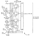
도 1은 일 실시예에 따라, 누설 전류를 감소시키는 시스템(150)을 구비한 예시적인 순차 회로(100)를 도시한다. 특히, 도 1은 파이프라인 형태의 순차 회로를 도시한다. 순차 회로(100)는 조합 논리 회로들(102A-N), 복수의 리셋 플립-플롭들(104A-N, 108A-N, 112A-N), 및 복수의 세트-리셋 플립-플롭들(106A-N, 110A-N, 114A-N)을 포함한다. 순차 회로(100)는 또한 제어 모듈(116)을 포함한다.1 illustrates an example
조합 논리 회로들(102A-N)은 복수의 논리 게이트들(예를 들면, AND, OR, NAND, NOR 등)을 조합하여 형성된 회로들이 될 수 있고, 조합 논리 회로들(102A-N)에 결합된 플립-플롭들로부터 수신된 입력들(120A-N, 122A-N)에 대한 불 대수(boolean algebra)를 수행하도록 구성된다. 일 예시적인 구현에서, 리셋 플립-플롭들(104A-N, 108A-N, 112A-N) 및 세트-리셋 플립-플롭들(106A-N, 110A-N, 114A-N)은 D형 플립-플롭들일 수 있다. 또한, 리셋 플립-플롭들(104A-N, 108A-N, 112A-N) 및 세트-리셋 플립-플롭들(106A-N, 110A-N, 114A-N)은 비동기 또는 동기 형태가 될 수 있다.
도시된 바와 같이, 리셋 플립-플롭들(104A-N) 및 세트-리셋 플립-플롭들(106A-N)은 조합 논리 회로(102A)에 결합된다. 또한, 리셋 플립-플롭들(108A-N) 및 세트-리셋 플립-플롭들(110A-N)은 조합 논리 회로(102A) 및 조합 논리 회로(102B)에 결합된다. 순차 회로(100)에서 2개의 인접한 조합 논리 회로들은 리셋 플립-플롭들 및 세트-리셋 플립-플롭들을 통해 접속되는 것을 유념할 수 있다. 또한, 도시된 바와 같이, 조합 논리 회로(102N)는 리셋 플립-플롭들(112A-N) 및 세트-리셋 플립-플롭들(114A-N)에 결합된다.As shown, reset flip-flops 104A-N and set-reset flip-flops 106A-N are coupled to
제어 모듈(116)은 리셋 플립-플롭들(104A-N, 108A-N, 112A-N) 및 세트-리셋 플립-플롭들(106A-N, 110A-N, 114A-N)에 결합된다. 일 예시적 실시예에서, 제어 모듈(116)은 리셋 플립-플롭들(104A-N, 108A-N, 112A-N)에 결합된 OR 게이트와, 세트-리셋 플립-플롭들(106A-N, 110A-N, 114A-N)에 결합된 AND 게이트를 포함한다. 제어 모듈(116), 리셋 플립-플롭들(104A-N), 세트-리셋 플립-플롭들(106A-N) 및 조합 논리 회로(102A)가 누설 전류를 감소시키는 시스템(150)을 형성하는 것을 도 1로부터 알 수 있다. 순차 회로(100)가 조합 논리 회로에 결합된 다중 단계들의 입력 플립-플롭들과 제어 모듈(116)을 포함할 수 있다는 것을 안다.Control module 116 is coupled to reset flip-flops 104A-N, 108A-N, 112A-N and set-reset flip-flops 106A-N, 110A-N, 114A-N. In one exemplary embodiment, the control module 116 includes an OR gate coupled to the reset flip-flops 104A-N, 108A-N, 112A-N, and the set-reset flip-flops 106A-N, And AND gates coupled to 110A-N, 114A-N. The control module 116, the reset flip-flops 104A-N, the set-reset flip-flops 106A-N, and the
순차 회로(100)의 활성 모드 동안, 입력들(120A-N)은 리셋 플립-플롭들(104A-N)에 각각 공급된다. 또한, 입력들(122A-N)은 세트-리셋 플립-플롭들(106A-N)에 각각 공급된다. 입력들(120A-N, 122A-N)을 이용하여, 리셋 플립-플롭들(104A-N) 및 세트-리셋 플립-플롭들(106A-N)은 조합 논리 회로(102A)를 구동한다. 조합 논리 회로(102A)의 출력들은 조합 논리 회로(102B)를 구동하기 위해 리셋 플립-플롭들(108A-N) 및 세트-리셋 플립-플롭들(110A-N)에 저장되거나 유지된다. 여러 단계들의 플립-플롭들 및 조합 논리 회로들을 통해 진행한 후에, 출력들(124A-N, 126A-N)이 생성된다.During the active mode of
순차 회로(100)의 대기 또는 슬립 모드(예를 들면, 또는 순차 회로(100)를 포함하는 디바이스)가 트리거될 때(예를 들면, 제어 신호(118)를 수신할 때), 제어 모듈(116)은 리셋 플립-플롭들(104A-N, 108A-N, 112A-N)을 리셋하고 세트-리셋 플립-플롭들(106A-N, 110A-N, 114A-N)을 세트하도록 구성된다. 제어 신호(118)(예를 들면, 활성 로우 슬립 신호)는 순차 회로(100)의 대기 또는 슬립 모드가 트리거될 때 제어 모듈(116)에 의해 수신되어 처리될 수 있다. 순차 회로(100)가 다시 활성이 될 때, 제어 모듈(116)은 투명하고 리셋 및 세트 신호들을 플립-플롭들에 넘겨준다.When the standby or sleep mode of the sequential circuit 100 (eg, or a device comprising the sequential circuit 100) is triggered (eg, when receiving a control signal 118), the control module 116 ) Is configured to reset the reset flip-flops 104A-N, 108A-N, 112A-N and set the set-reset flip-flops 106A-N, 110A-N, 114A-N. Control signal 118 (eg, an active low sleep signal) may be received and processed by control module 116 when the standby or sleep mode of
본 발명의 실시예에 따라, 다음의 처리가 순차 회로(100)의 설계 동안에 이용될 수 있다. 순차 회로(100)를 설계하기 위하여, 동기화되고, 맵핑되고 타이밍 정지된 넷리스트(netlist)가 논리 합성 도구로부터 입력으로 취해진다. 모든 조합 논리 회로들(102A-N)에 대해, 최소 누설 비트들(MLB들)이 입력 벡터 제어 방법을 이용하여 계산되며, 이 방법은 본 기술분야의 통상의 지식을 가진 기술자에게 잘 알려져 있다. 그 후에, 논리값 '1'의 MLB를 유발하는 순차 회로(100)에서의 리셋 플립-플롭들은 세트-리셋 플립-플롭들(예를 들면, 세트-리셋 플립-플롭들(106A-N, 110A-N, 114A-N))로 대체된다. 리셋 플립-플롭들을 세트-리셋 플립-플롭들(106A-N, 110A-N, 114A-N)로 대체하기 위해, 리셋 플립-플롭들이 합성 처리에 앞서 활성 로우 리셋을 가진다고 가정한다.In accordance with an embodiment of the present invention, the following processing may be used during the design of the
그 후에, 논리값 '0'의 MLB를 가진 리셋 플립-플롭들(예를 들면, 리셋 플립-플롭들(104A-N, 108A-N, 112A-N))의 리셋 핀들은 활성 로우 슬립 신호에 논리적으로 접속된다. 세트-리셋 플립-플롭들(106A-N, 110A-N, 114A-N)의 리셋 핀들의 접속은 변하지 않은 상태로 남아 있다는 것을 유념할 수 있다. 달리 말하면, 세트-리셋 플립-플롭들(106A-N, 110A-N, 114A-N)의 리셋 핀들은 리셋 신호에 접속된다. 또한, 세트-리셋 플립-플롭들(106A-N, 110A-N, 114A-N)의 세트 핀들이 함께 연결되어, 순차 회로(100)가 대기 모드에 들어갈 때 반전된 슬립 신호가 세트 핀들에 공급될 수 있다.Thereafter, reset pins of reset flip-flops (e.g., reset flip-flops 104A-N, 108A-N, 112A-N) with MLB of logic '0' are applied to the active low sleep signal. Logically connected It may be noted that the connection of the reset pins of the set-reset flip-flops 106A-N, 110A-N, 114A-N remains unchanged. In other words, the reset pins of the set-reset flip-flops 106A-N, 110A-N, 114A-N are connected to the reset signal. In addition, the set pins of the set-reset flip-flops 106A-N, 110A-N, and 114A-N are connected together so that an inverted sleep signal is supplied to the set pins when the
그 후에, 정적 타이밍 분석(STA: static timing analysis)이 수정된 넷리스트에 대해 수행된다. 세트-리셋 플립-플롭들(106A-N, 110A-N, 114A-N)의 삽입에 의해 유발된 어떤 변형들의 경우에, 세트-리셋 플립-플롭들(106A-N, 110A-N, 114A-N)은 등가의 리셋 플립-플롭들에 의해 대체된다는 것을 유념할 수 있다. STA를 수행할 때, 수정된 넷리스트는 순차 회로(100)의 설계를 완료하기 위한 물리적 설계 도구에 공급된다. 최종적으로, 도 1에 도시된 바와 같은 순차 회로(100)가 얻어진다.After that, static timing analysis (STA) is performed on the modified netlist. In the case of certain variations caused by the insertion of the set-reset flip-flops 106A-N, 110A-N, 114A-N, the set-reset flip-flops 106A-N, 110A-N, 114A- It can be noted that N) is replaced by equivalent reset flip-flops. When performing the STA, the modified netlist is supplied to a physical design tool for completing the design of the
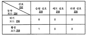
도 2a는 일 실시예에 따라 도 1의 시스템(150)의 예시적인 회로(200)를 도시한다. 도시된 바와 같이, 회로(200)는 조합 논리 회로(202), 비동기 리셋 플립-플롭들(204A-N) 및 비동기 세트-리셋 플립-플롭들(206A-N)을 포함한다. 회로(200)는 또한, OR 게이트(208) 및 AND 게이트(210)를 포함한다. OR 게이트(208) 및 AND 게이트(210)는 함께 도 1의 제어 모듈(116)을 구성한다는 것을 안다.FIG. 2A illustrates an
도 2a에서, 비동기 리셋 플립-플롭들(204A-N) 및 비동기 세트-리셋 플립-플롭들(206A-N)은 조합 논리 회로(202)에 결합된다. OR 게이트(208)의 출력은 비동기 세트-리셋 플립-플롭들(206A-N)에 결합된다. 또한, OR 게이트(208)는 제 1 입력 노드(214) 및 제 2 입력 노드(216)를 포함하며, 제 1 입력 노드(214)는 세트 신호(218)를 수신하도록 구성되고, 제 2 입력 노드(216)는 슬립 신호(220)를 수신하도록 구성된다. AND 게이트의 출력은 비동기 리셋 플립-플롭들(204A-N)에 결합된다. 또한, AND 게이트(210)는 제 1 입력 단자(222) 및 제 2 입력 단자(224)를 포함하고, 제 1 입력 단자(222)는 슬립 신호(220)를 수신하도록 구성되고, 제 2 입력 단자(224)는 리셋 신호(226)를 수신하도록 구성된다.In FIG. 2A, asynchronous reset flip-flops 204A-N and asynchronous set-reset flip-flops 206A-N are coupled to
도시된 바와 같이, 비동기 리셋 플립-플롭들(204A-N) 및 비동기 세트-리셋 플립-플롭들(206A-N)은 입력들(228)을 수신하도록 구성된다. 활성 모드 동안, 비동기 리셋 플립-플롭들(204A-N) 및 비동기 세트-리셋 플립-플롭들(206A-N)은 출력들(230)을 생성하기 위해 입력들(228)을 조합 논리 회로(202)에 공급한다. 그 후에, 출력들(230)은 순차 회로(100)의 후속 단계들에 입력들로서 공급된다. 대기 동작 모드 동안, 비동기 리셋 플립-플롭들(204A-N) 및 비동기 세트-리셋 플립-플롭들(206A-N)은 최소 누설 비트들(212)(예를 들면, 0 또는 1)을 조합 논리 회로(202)에 공급한다. 최소 누설 비트들(212)은 입력 벡터 제어 방법을 이용하여 얻어진다는 것을 안다. 또한, 최소 누설 비트들(212)은 대기 동작 모드 동안 조합 논리 회로(202)를 통해 최소 누설 전류를 제공하기 위해 이용된다는 것을 안다.As shown, asynchronous reset flip-flops 204A-N and asynchronous set-reset flip-flops 206A-N are configured to receive inputs 228. During active mode, asynchronous reset flip-flops 204A-N and asynchronous set-reset flip-flops 206A-N combine inputs 228 with
도 2b는 일 실시예에 따라, 도 2a의 회로(200)의 동작을 도시하는 예시적인 테이블(250)을 도시한다. 테이블(250)은 3개 형태들의 신호(252)와 2개 형태들의 동작 모드(254)를 도시한다. 테이블(250)에 도시된 바와 같이, 회로(200)가 대기 모드(256)로 진입하도록 트리거될 때, OR 게이트(208)는 제 2 입력 노드(216)를 통해 활성 로우 슬립 신호(예를 들면, 논리값 '0'의)를 반전 및 처리하도록 구성된다. 따라서, OR 게이트(208)는 비동기 세트-리셋 플립-플롭들(206A-N)을 세트한다. 결과적으로, 비동기 세트-리셋 플립-플롭들(206A-N)은, 조합 논리 회로(202)를 통한 누설 전류가 최소가 되도록, 최소 누설 비트들(212)(예를 들면, 값 1의)을 조합 논리 회로(202)에 공급한다.FIG. 2B shows an exemplary table 250 illustrating the operation of the
또한, AND 게이트(210)는 비동기 리셋 플립-플롭들(204A-N)을 리셋하기 위해 제 1 입력 단자(222)를 통해 활성 로우 슬립 신호(220)(예를 들면, 논리값 '0'의)를 처리하도록 구성된다. 이것은, 조합 논리 회로(202)를 통한 누설 전류가 최소가 되도록, 비동기 리셋 플립-플롭들(204A-N)로 하여금 최소 누설 비트들(212)(예를 들면 값 0의)을 조합 논리 회로(202)에 공급하게 한다. In addition, AND gate 210 is configured to reset active low sleep signal 220 (eg, a logic value '0' through first input terminal 222 to reset asynchronous reset flip-flops 204A-N. Is configured to handle This causes the asynchronous reset flip-flops 204A-N to set the minimum leakage bits 212 (eg of value 0) so that the leakage current through the
활성 모드(258)가 트리거될 때, OR 게이트(208)는 제 1 입력 노드(214)를 통해 세트 신호(218)를 처리하고, 제 2 입력 노드(216)를 통해 하이 슬립 신호(220)(예를 들면, 논리값 '1'의)를 처리하도록 구성된다. 따라서, OR 게이트(208)는 세트 신호(218)를 비동기 세트-리셋 플립-플롭들(206A-N)에 넘겨준다. 또한, AND 게이트(210)는 제 1 입력 단자(222)를 통해 하이 슬립 신호(220)(예를 들면, 논리값 '1'의)를 처리하고 제 2 입력 단자(224)를 통해 리셋 신호(226)를 처리하도록 구성된다. 따라서, AND 게이트(210)는 리셋 신호(226)를 비동기 리셋 플립-플롭들(204A-N)에 넘겨준다. 즉, OR 게이트(208) 및 AND 게이트(210)를 포함하는 제어 모듈은 세트 신호(218) 및 리셋 신호(226)를 플립-플롭들에 넘긴 이후, 활성 모드(258) 동안 투명해진다. 따라서, 회로(200)의 활성 모드(258)가 트리거되고 세트 신호(218) 및 리셋 신호(226)가 존재하지 않을 때, 비동기 리셋 플립-플롭들(204A-N) 및 비동기 세트-리셋 플립-플롭들(206A-N)은 입력들(228)을 조합 논리 회로(202)에 공급한다. 결과적으로, 조합 논리 회로(202)는 순차 회로(100)의 후속 단계(들)에 제공될 출력들(230)을 생성한다.When active mode 258 is triggered, OR gate 208 processes set
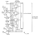
도 3a는 일 실시예에 따라 도 1의 시스템(150)의 예시적인 회로(300)를 도시한다. 도시된 바와 같이, 회로(300)는 조합 논리 회로(302), 동기 리셋 플립-플롭들(304A-N) 및 동기 세트-리셋 플립-플롭들(306A-N)을 포함한다. 회로(300)는 또한, OR 게이트(308) 및 AND 게이트(310)를 포함한다. OR 게이트(308) 및 AND 게이트(310)는 함께 도 1의 제어 모듈(116)을 구성한다는 것을 안다.3A illustrates an
도 3a에서, 동기 리셋 플립-플롭들(304A-N) 및 동기 세트-리셋 플립-플롭들(306A-N)은 조합 논리 회로(302)에 결합된다. OR 게이트(308)의 출력은 동기 세트-리셋 플립-플롭들(306A-N)에 결합된다. 또한, OR 게이트(308)는 제 1 입력 노드(314) 및 제 2 입력 노드(316)를 포함하며, 제 1 입력 노드(314)는 세트 신호(318)를 수신하도록 구성되고, 제 2 입력 노드(316)는 슬립 신호(320)를 수신하도록 구성된다. AND 게이트(310)의 출력은 동기 리셋 플립-플롭들(304A-N)에 결합된다. 또한, AND 게이트(310)는 제 1 입력 단자(322) 및 제 2 입력 단자(324)를 포함하고, 제 1 입력 단자(322)는 슬립 신호(320)를 수신하도록 구성되고, 제 2 입력 단자(324)는 리셋 신호(326)를 수신하도록 구성된다.In FIG. 3A, synchronous reset flip-flops 304A-N and synchronous set-reset flip-flops 306A-N are coupled to
도시된 바와 같이, 동기 리셋 플립-플롭들(304A-N) 및 동기 세트-리셋 플립-플롭들(306A-N)은 입력들(328)을 수신하도록 구성된다. 활성 모드 동안, 동기 리셋 플립-플롭들(304A-N) 및 동기 세트-리셋 플립-플롭들(306A-N)은 출력들(330)을 생성하기 위해 입력들(328)을 조합 논리 회로(302)에 공급한다. 그 후에, 출력들(330)은 순차 회로(100)의 후속 단계들에 입력들로서 공급된다. 대기 모드 동안, 동기 리셋 플립-플롭들(304A-N) 및 동기 세트-리셋 플립-플롭들(306A-N)은 최소 누설 비트들(312)(예를 들면, 0 또는 1)을 조합 논리 회로(302)에 공급한다. 최소 누설 비트들(312)은 입력 벡터 제어 방법을 이용하여 얻어진다는 것을 안다. 또한, 최소 누설 비트들(312)은 대기 동작 모드 동안 조합 논리 회로(302)를 통해 최소 누설 전류를 제공하기 위해 이용된다는 것을 안다.As shown, synchronous reset flip-flops 304A-N and synchronous set-reset flip-flops 306A-N are configured to receive inputs 328. During active mode, synchronous reset flip-flops 304A-N and synchronous set-reset flip-flops 306A-N combine inputs 328 with
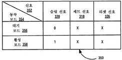
도 3b는 일 실시예에 따라, 도 3a의 회로(300)의 동작을 도시하는 예시적인 테이블(350)을 도시한다. 테이블(350)은 3개 형태들의 신호(352)와 2개 형태들의 동작 모드(354)를 도시한다. 테이블(350)에 도시된 바와 같이, 회로(300)의 대기 모드(356) 및 활성 모드(358) 동안 회로(300)의 동작은 테이블(250)에 도시된 회로(200)의 동작과 동일하므로, 그 기술은 생략된다.FIG. 3B shows an example table 350 illustrating the operation of the
도 4는 일 실시예에 따라, 도 1의 순차 회로(100)를 가진 예시적인 디바이스(400)를 도시한다. 도 4에 도시된 바와 같은 디바이스(400)는 랩탑, 모바일 디바이스, 워크스테이션, 서버, 데스크탑 등과 같은, 순차 회로(100)를 이용하는 임의의 전자 디바이스가 될 수 있다. 도시된 바와 같이, 디바이스(400)는 제어 모듈(116)(예를 들면, 도 1에 도시된 바와 같이)을 가진 순차 회로(100)와 전력 관리 유닛(402)을 포함한다. 전력 관리 유닛(402)은 제어 모듈(116)에 결합된다. 일 예시적인 구현에서, 전력 관리 유닛(402)은 디바이스(400)의 대기 모드가 트리거될 때, 슬립 신호(404)(예를 들면, 활성 로우 슬립 신호)를 생성한다. 또한, 전력 관리 유닛(402)은 제어 모듈(116)에 슬립 신호(404)를 전송한다. 상술된 바와 같이, 제어 모듈(116)은, 조합 논리 회로들(102A-N)을 통한 누설 전류가 최소가 되도록, 슬립 신호(404)를 수신할 때 리셋 플립-플롭들(104A-N, 108A-N, 112A-N)을 리셋하고 세트-리셋 플립-플롭들(106A-N, 110A-N, 114A-N)을 세트한다.4 illustrates an
다양한 실시예들에서, 도 1 내지 도 4에 기술된 시스템들 및 디바이스들은, 순차 회로에서 상당한 수의 추가적 구성요소들(예를 들면, 멀티플렉서들, 논리 게이트들 등)을 이용하지 않고 MLB들에 기초하여 리셋 및 세트-리셋 플립 플롭들을 구현함으로써 순차 회로에서 누설 전류를 감소시키도록 도울 수 있다. 또한, 시스템들 및 디바이스들은 메모리에 MLB들을 저장할 필요성을 제거할 수 있다. 또한, 시스템들 및 디바이스들은 순차 회로가 대기 모드로 진입한 직후 클록을 차단하도록 허용할 수 있고, 따라서, 상당량의 동적 전력을 절감한다.In various embodiments, the systems and devices described in FIGS. 1-4 may be coupled to MLBs without using a significant number of additional components (eg, multiplexers, logic gates, etc.) in a sequential circuit. Implementing reset and set-reset flip flops based may help reduce leakage current in sequential circuitry. Also, systems and devices can eliminate the need to store MLBs in memory. Also, systems and devices can allow the sequential circuit to shut off the clock immediately after entering standby mode, thus saving a significant amount of dynamic power.
본 실시예들이 특정 예시적인 실시예들을 참조하여 기술되었지만, 다양한 실시예들의 더욱 광범위한 기술사상 및 범주를 벗어나지 않고 이들 실시예들에 대한 다양한 수정들 및 변경들이 이루어질 수 있다는 것이 명백할 것이다. 예를 들면, 본 명세서에 기술된 다양한 디바이스들, 모듈들, 분석기들, 생성기들 등은 하드웨어 회로(예를 들면, 상보성 금속-산화물-반도체(CMOS) 기반 논리 회로), 펌웨어, 소프트웨어, 및/또는 하드웨어, 펌웨어, 및/또는 소프트웨어(예를 들면, 기계 판독 가능한 매체에서 구현됨)의 임의의 조합을 이용하여 가능하게 되고 동작될 수 있다. 예를 들면, 다양한 전기 구조 및 방법들은 트랜지스터들, 논리 게이트들, 및 전기 회로들(예를 들면, 주문형 반도체 회로(ASIC))을 이용하여 구현될 수 있다.While the present embodiments have been described with reference to specific example embodiments, it will be apparent that various modifications and changes may be made to these embodiments without departing from the broader spirit and scope of the various embodiments. For example, the various devices, modules, analyzers, generators, etc. described herein may be hardware circuitry (eg, complementary metal-oxide-semiconductor (CMOS) based logic circuits), firmware, software, and / Or may be enabled and operated using any combination of hardware, firmware, and / or software (eg, implemented on a machine readable medium). For example, various electrical structures and methods may be implemented using transistors, logic gates, and electrical circuits (eg, application specific semiconductor circuits (ASICs)).
118 : 제어 신호
116 : 제어 모듈
106A : 세트-리셋 플립-플롭
120A : 입력
104A : 리셋 플립-플롭
120N : 입력
104N : 리셋 플립-플롭
122A : 입력
122N : 입력
106N : 세트-리셋 플립-플롭
102A : 순차 논리 회로
108A : 리셋 플립-플롭
108N : 리셋 플립-플롭
110A : 세트-리셋 플립-플롭
110N : 세트-리셋 플립-플롭
102B : 순차 논리 회로
102N : 순차 논리 회로
112A : 리셋 플립-플롭
124A : 출력
112N : 리셋 플립-플롭
124N : 출력
126A : 출력
114A : 세트-리셋 플립-플롭
126N : 출력
114N : 세트-리셋 플립-플롭
150 : 누설 전류를 감소시키는 시스템118: control signal
116: control module
106A: Set-Reset Flip-Flops
120A: input
104A: Reset Flip-Flop
120N: input
104N: Reset Flip-Flop
122A: input
122N: input
106N: Set-Reset Flip-Flops
102A: Sequential Logic Circuit
108A: Reset Flip-Flop
108N: Reset Flip-Flop
110A: Set-Reset Flip-Flops
110N: Set-Reset Flip-Flop
102B: Sequential Logic Circuit
102N: Sequential Logic Circuit
112A: Reset Flip-Flop
124A: Output
112N: Reset Flip-Flop
124N: output
126A: output
114A: Set-Reset Flip-Flops
126N: output
114N: Set-Reset Flip-Flops
150: system for reducing leakage current
Claims (20)
조합 논리 회로;
상기 조합 논리 회로에 결합된 적어도 하나의 리셋 플립-플롭;
상기 조합 논리 회로에 결합된 적어도 하나의 세트-리셋 플립-플롭; 및
상기 적어도 하나의 리셋 플립-플롭 및 상기 적어도 하나의 세트 플립-플롭에 결합되고, 상기 순차 회로의 대기 모드가 트리거될 때 상기 적어도 하나의 리셋 플립-플롭을 리셋하고 상기 적어도 하나의 세트-리셋 플립-플롭을 세트하도록 구성된 제어 모듈을 포함하는, 누설 전류 감소 시스템.In a system that reduces leakage current in a sequential circuit:
Combinational logic circuits;
At least one reset flip-flop coupled to the combinational logic circuit;
At least one set-reset flip-flop coupled to the combinational logic circuit; And
Coupled to the at least one reset flip-flop and the at least one set flip-flop, reset the at least one reset flip-flop and trigger the at least one set-reset flip when a standby mode of the sequential circuit is triggered A leakage current reduction system comprising a control module configured to set a flop.
상기 적어도 하나의 리셋 플립-플롭은 적어도 하나의 비동기 리셋 플립-플롭을 포함하고, 상기 적어도 하나의 세트-리셋 플립-플롭은 적어도 하나의 비동기 세트-리셋 플립-플롭을 포함하는, 누설 전류 감소 시스템.The method of claim 1,
The at least one reset flip-flop comprises at least one asynchronous reset flip-flop, and the at least one set-reset flip-flop comprises at least one asynchronous set-reset flip-flop .
상기 적어도 하나의 리셋 플립-플롭은 적어도 하나의 동기 리셋 플립-플롭을 포함하고, 상기 적어도 하나의 세트-리셋 플립-플롭은 적어도 하나의 동기 세트-리셋 플립-플롭을 포함하는, 누설 전류 감소 시스템.The method of claim 1,
The at least one reset flip-flop comprises at least one synchronous reset flip-flop, and the at least one set-reset flip-flop comprises at least one synchronous set-reset flip-flop .
상기 적어도 하나의 리셋 플립-플롭 및 상기 적어도 하나의 세트-리셋 플립-플롭은 상기 대기 모드 동안 상기 조합 논리 회로에 최소 누설 비트들(minimum leakage bits)을 공급하도록 구성되는, 누설 전류 감소 시스템.The method of claim 1,
And the at least one reset flip-flop and the at least one set-reset flip-flop are configured to supply minimum leakage bits to the combinational logic circuit during the standby mode.
상기 최소 누설 비트들은 상기 조합 논리 회로를 통해 최소 누설 전류를 제공하기 위해 이용되는, 누설 전류 감소 시스템.The method of claim 4, wherein
The minimum leakage bits are used to provide a minimum leakage current through the combinational logic circuit.
상기 최소 누설 비트들은 입력 벡터 제어 방법을 이용하여 얻어지는, 누설 전류 감소 시스템.The method of claim 4, wherein
Wherein the minimum leakage bits are obtained using an input vector control method.
상기 제어 모듈은:
상기 적어도 하나의 세트-리셋 플립-플롭에 결합된 OR 게이트; 및
상기 적어도 하나의 리셋 플립-플롭에 결합된 AND 게이트를 포함하는, 누설 전류 감소 시스템.The method of claim 1,
The control module is:
An OR gate coupled to the at least one set-reset flip-flop; And
And an AND gate coupled to the at least one reset flip-flop.
상기 OR 게이트는 상기 순차 회로의 상기 대기 모드가 트리거될 때 수신되는 활성 로우 슬립 신호(active low sleep signal)에 기초하여, 상기 적어도 하나의 세트-리셋 플립-플롭을 세트하도록 구성되는, 누설 전류 감소 시스템.The method of claim 7, wherein
The OR gate is configured to set the at least one set-reset flip-flop based on an active low sleep signal received when the standby mode of the sequential circuit is triggered system.
상기 OR 게이트는 제 1 입력 노드 및 제 2 입력 노드를 포함하고, 상기 OR 게이트는 상기 제 2 입력 노드를 통해 상기 활성 로우 슬립 신호를 반전 및 처리하도록 구성되는, 누설 전류 감소 시스템.The method of claim 8,
The OR gate includes a first input node and a second input node, and the OR gate is configured to invert and process the active low sleep signal through the second input node.
상기 OR 게이트는 상기 순차 회로의 활성 모드가 트리거될 때, 상기 제 2 입력 노드를 통해 하이 슬립 신호를 반전 및 처리하도록 구성되는, 누설 전류 감소 시스템.The method of claim 9,
The OR gate is configured to invert and process a high sleep signal through the second input node when an active mode of the sequential circuit is triggered.
상기 AND 게이트는 상기 순차 회로의 상기 대기 모드가 트리거될 때 수신되는 활성 로우 슬립 신호에 기초하여 상기 적어도 하나의 리셋 플립-플롭을 리셋하도록 구성되는, 누설 전류 감소 시스템.The method of claim 7, wherein
And the AND gate is configured to reset the at least one reset flip-flop based on an active low sleep signal received when the standby mode of the sequential circuit is triggered.
상기 AND 게이트는 제 1 입력 단자 및 제 2 입력 단자를 포함하고, 상기 AND 게이트는 상기 제 1 단자를 통해 상기 활성 로우 슬립 신호를 처리하도록 구성되는, 누설 전류 감소 시스템.The method of claim 11,
And the AND gate includes a first input terminal and a second input terminal, and the AND gate is configured to process the active low sleep signal through the first terminal.
상기 AND 게이트는 상기 순차 회로의 활성 모드가 트리거될 때 상기 제 1 입력 단자를 통해 하이 슬립 신호를 처리하도록 구성되는, 누설 전류 감소 시스템.The method of claim 12,
And the AND gate is configured to process a high sleep signal through the first input terminal when an active mode of the sequential circuit is triggered.
복수의 조합 논리 회로들;
상기 복수의 조합 논리 회로들의 각각에 결합된 적어도 하나의 리셋 플립-플롭;
상기 복수의 조합 논리 회로들의 각각에 결합된 적어도 하나의 세트-리셋 플립-플롭; 및
상기 적어도 하나의 리셋 플립-플롭 및 상기 적어도 하나의 세트-리셋 플립-플롭에 결합되고, 상기 순차 회로의 대기 모드가 트리거될 때 상기 적어도 하나의 리셋 플립-플롭을 리셋하고 상기 적어도 하나의 세트-리셋 플립-플롭을 세트하도록 구성된 제어 모듈을 포함하는, 순차 회로.In a sequential circuit:
A plurality of combinational logic circuits;
At least one reset flip-flop coupled to each of the plurality of combinational logic circuits;
At least one set-reset flip-flop coupled to each of the plurality of combinational logic circuits; And
Coupled to the at least one reset flip-flop and the at least one set-reset flip-flop, and reset the at least one reset flip-flop when the standby mode of the sequential circuit is triggered and the at least one set- And a control module configured to set a reset flip-flop.
상기 적어도 하나의 리셋 플립-플롭 및 상기 적어도 하나의 세트-리셋 플립-플롭의 각각은 D형 플립-플롭에 기초하는, 순차 회로.The method of claim 14,
Each of the at least one reset flip-flop and the at least one set-reset flip-flop is based on a D-type flip-flop.
상기 적어도 하나의 리셋 플립-플롭은 적어도 하나의 비동기 리셋 플립-플롭을 포함하고, 상기 적어도 하나의 세트-리셋 플립-플롭은 적어도 하나의 비동기 세트-리셋 플립-플롭을 포함하는, 순차 회로.The method of claim 14,
The at least one reset flip-flop comprises at least one asynchronous reset flip-flop, and the at least one set-reset flip-flop comprises at least one asynchronous set-reset flip-flop.
상기 적어도 하나의 리셋 플립-플롭은 적어도 하나의 동기 리셋 플립-플롭을 포함하고, 상기 적어도 하나의 세트-리셋 플립-플롭은 적어도 하나의 동기 세트-리셋 플립-플롭을 포함하는, 순차 회로.The method of claim 14,
The at least one reset flip-flop comprises at least one synchronous reset flip-flop, and the at least one set-reset flip-flop comprises at least one synchronous set-reset flip-flop.
상기 제어 모듈은:
상기 적어도 하나의 세트-리셋 플립-플롭에 결합된 OR 게이트; 및
상기 적어도 하나의 리셋 플립-플롭에 결합된 AND 게이트를 포함하는, 순차 회로.The method of claim 14,
The control module is:
An OR gate coupled to the at least one set-reset flip-flop; And
And an AND gate coupled to the at least one reset flip-flop.
상기 순차 회로는:
복수의 조합 논리 회로들;
상기 복수의 조합 논리 회로들의 각각에 결합된 적어도 하나의 리셋 플립-플롭;
상기 복수의 조합 논리 회로들의 각각에 결합된 적어도 하나의 세트-리셋 플립-플롭; 및
상기 적어도 하나의 리셋 플립-플롭 및 상기 적어도 하나의 세트-리셋 플립-플롭에 결합되고, 상기 순차 회로의 대기 모드가 트리거될 때 상기 적어도 하나의 리셋 플립-플롭을 리셋하고 상기 적어도 하나의 세트-리셋 플립-플롭을 세트하도록 구성된 제어 모듈을 포함하는, 디바이스.In a device comprising a sequential circuit:
The sequential circuit is:
A plurality of combinational logic circuits;
At least one reset flip-flop coupled to each of the plurality of combinational logic circuits;
At least one set-reset flip-flop coupled to each of the plurality of combinational logic circuits; And
Coupled to the at least one reset flip-flop and the at least one set-reset flip-flop, and reset the at least one reset flip-flop when the standby mode of the sequential circuit is triggered and the at least one set- And a control module configured to set a reset flip-flop.
상기 제어 모듈에 결합되어, 상기 순차 회로의 상기 대기 모드가 트리거될 때 슬립 신호를 전송하기 위한 전력 관리 유닛을 더 포함하는, 디바이스.The method of claim 19,
And a power management unit, coupled to the control module, for transmitting a sleep signal when the standby mode of the sequential circuit is triggered.
Applications Claiming Priority (2)
| Application Number | Priority Date | Filing Date | Title |
|---|---|---|---|
| US12/640,004 US8736332B2 (en) | 2009-12-17 | 2009-12-17 | Leakage current reduction in a sequential circuit |
| US12/640,004 | 2009-12-17 |
Publications (1)
| Publication Number | Publication Date |
|---|---|
| KR20110069664A true KR20110069664A (en) | 2011-06-23 |
Family
ID=42514259
Family Applications (1)
| Application Number | Title | Priority Date | Filing Date |
|---|---|---|---|
| KR1020100014991A KR20110069664A (en) | 2009-12-17 | 2010-02-19 | Leakage current reduction in a sequential circuit |
Country Status (6)
| Country | Link |
|---|---|
| US (1) | US8736332B2 (en) |
| EP (1) | EP2339752B1 (en) |
| JP (1) | JP5462703B2 (en) |
| KR (1) | KR20110069664A (en) |
| CN (1) | CN101777908A (en) |
| TW (1) | TW201123731A (en) |
Cited By (1)
| Publication number | Priority date | Publication date | Assignee | Title |
|---|---|---|---|---|
| KR20160079402A (en) * | 2014-12-26 | 2016-07-06 | 전자부품연구원 | Sequential circuit design method and clock gating circuit |
Families Citing this family (7)
| Publication number | Priority date | Publication date | Assignee | Title |
|---|---|---|---|---|
| US8307226B1 (en) * | 2011-12-20 | 2012-11-06 | Intel Corporation | Method, apparatus, and system for reducing leakage power consumption |
| US9100002B2 (en) | 2013-09-12 | 2015-08-04 | Micron Technology, Inc. | Apparatus and methods for leakage current reduction in integrated circuits |
| US9496851B2 (en) * | 2014-09-10 | 2016-11-15 | Qualcomm Incorporated | Systems and methods for setting logic to a desired leakage state |
| US9601477B2 (en) * | 2014-12-18 | 2017-03-21 | Marvell World Trade Ltd. | Integrated circuit having spare circuit cells |
| US9503086B1 (en) * | 2015-09-16 | 2016-11-22 | Apple Inc. | Lockup latch for subthreshold operation |
| CN105515565B (en) * | 2015-12-14 | 2018-07-13 | 天津光电通信技术有限公司 | A kind of method that hardware logic resource multiplex module and multiplexing are realized |
| US10423203B2 (en) * | 2016-12-28 | 2019-09-24 | Intel Corporation | Flip-flop circuit with low-leakage transistors |
Family Cites Families (13)
| Publication number | Priority date | Publication date | Assignee | Title |
|---|---|---|---|---|
| TW392307B (en) * | 1998-01-13 | 2000-06-01 | Mitsubishi Electric Corp | A method of the manufacture and the setup of the semiconductor apparatus |
| JPH11340812A (en) | 1998-05-22 | 1999-12-10 | Mitsubishi Electric Corp | Semiconductor device |
| US6191606B1 (en) | 1998-09-10 | 2001-02-20 | Intel Corporation | Method and apparatus for reducing standby leakage current using input vector activation |
| US6169419B1 (en) | 1998-09-10 | 2001-01-02 | Intel Corporation | Method and apparatus for reducing standby leakage current using a transistor stack effect |
| US7302652B2 (en) | 2003-03-31 | 2007-11-27 | Intel Corporation | Leakage control in integrated circuits |
| US7096374B2 (en) | 2003-05-21 | 2006-08-22 | Agilent Technologies, Inc. | Method and apparatus for defining an input state vector that achieves low power consumption in digital circuit in an idle state |
| KR100574967B1 (en) | 2004-01-29 | 2006-04-28 | 삼성전자주식회사 | Controller for Multi-Threshold CMOS |
| US7305335B2 (en) * | 2004-11-23 | 2007-12-04 | Schweitzer Engineering Laboratories, Inc. | Permanent three-pole independent pole operation recloser simulator feature in a single-pole trip capable recloser control |
| US20070168792A1 (en) | 2005-12-09 | 2007-07-19 | International Business Machines Corporation | Method to Reduce Leakage Within a Sequential Network and Latch Circuit |
| JP4953716B2 (en) * | 2006-07-25 | 2012-06-13 | パナソニック株式会社 | Semiconductor integrated circuit and related technology |
| US7949971B2 (en) | 2007-03-27 | 2011-05-24 | International Business Machines Corporation | Method and apparatus for on-the-fly minimum power state transition |
| GB2447944B (en) * | 2007-03-28 | 2011-06-29 | Advanced Risc Mach Ltd | Reducing leakage power in low power mode |
| US7735045B1 (en) * | 2008-03-12 | 2010-06-08 | Xilinx, Inc. | Method and apparatus for mapping flip-flop logic onto shift register logic |
-
2009
- 2009-12-17 US US12/640,004 patent/US8736332B2/en active Active
-
2010
- 2010-02-11 CN CN201010109303.9A patent/CN101777908A/en active Pending
- 2010-02-19 KR KR1020100014991A patent/KR20110069664A/en not_active Application Discontinuation
- 2010-03-30 EP EP10158485.2A patent/EP2339752B1/en not_active Not-in-force
- 2010-05-13 JP JP2010111048A patent/JP5462703B2/en not_active Expired - Fee Related
- 2010-05-24 TW TW099116527A patent/TW201123731A/en unknown
Cited By (1)
| Publication number | Priority date | Publication date | Assignee | Title |
|---|---|---|---|---|
| KR20160079402A (en) * | 2014-12-26 | 2016-07-06 | 전자부품연구원 | Sequential circuit design method and clock gating circuit |
Also Published As
| Publication number | Publication date |
|---|---|
| EP2339752A1 (en) | 2011-06-29 |
| JP2011130405A (en) | 2011-06-30 |
| US8736332B2 (en) | 2014-05-27 |
| CN101777908A (en) | 2010-07-14 |
| JP5462703B2 (en) | 2014-04-02 |
| US20110148496A1 (en) | 2011-06-23 |
| TW201123731A (en) | 2011-07-01 |
| EP2339752B1 (en) | 2014-05-21 |
Similar Documents
| Publication | Publication Date | Title |
|---|---|---|
| KR20110069664A (en) | Leakage current reduction in a sequential circuit | |
| US7977972B2 (en) | Ultra-low power multi-threshold asynchronous circuit design | |
| US9331680B2 (en) | Low power clock gated flip-flops | |
| US9350327B2 (en) | Flip-flops with low clock power | |
| KR960027335A (en) | Dynamic, Clocked Inverter Latch Reduces Leakage Charge | |
| US9246489B1 (en) | Integrated clock gating cell using a low area and a low power latch | |
| CN106487361B (en) | Multi-bit flip-flop with shared clock switch | |
| US9425771B2 (en) | Low area flip-flop with a shared inverter | |
| US9083337B2 (en) | Multi-threshold sleep convention logic without nsleep | |
| KR20170043995A (en) | Apparatus for low power high speed integrated clock gating cell | |
| US11092649B2 (en) | Method for reducing power consumption in scannable flip-flops without additional circuitry | |
| KR20200110161A (en) | Low power integrated clock gating system and method | |
| US11575366B2 (en) | Low power flip-flop | |
| US7986166B1 (en) | Clock buffer circuit | |
| US10706916B1 (en) | Method and apparatus for integrated level-shifter and memory clock | |
| Lin et al. | Low voltage adiabatic flip-flops based on power-gating CPAL circuits | |
| US6853229B2 (en) | Circuit for transforming a single ended signal into a differential mode signal | |
| TWI836012B (en) | Apparatus for reducing power consumption and scan chain flip-flop | |
| KR20090045363A (en) | Static pulsed bus circuit and method having dynamic power supply rail selection | |
| Smith et al. | Low-Power NCL Design | |
| Srilakshmi et al. | Static power optimization using dual sub-threshold supply voltages in digital CMOS VLSI circuits | |
| Andrawes et al. | Null Convention logic circuits using balanced ternary on SOI | |
| Koteswara Rao et al. | Low power register design with integration clock gating and power gating | |
| DHANJAL et al. | Optimization of Power in Flip-Flop Group using Clock Gating and Power Gating with Variable Body-Bias Technique | |
| KALYANI et al. | Investigation on Performance of high speed CMOS Full adder Circuits |
Legal Events
| Date | Code | Title | Description |
|---|---|---|---|
| WITN | Application deemed withdrawn, e.g. because no request for examination was filed or no examination fee was paid |