KR20110031957A - Light converting construction - Google Patents
Light converting construction Download PDFInfo
- Publication number
- KR20110031957A KR20110031957A KR1020117001595A KR20117001595A KR20110031957A KR 20110031957 A KR20110031957 A KR 20110031957A KR 1020117001595 A KR1020117001595 A KR 1020117001595A KR 20117001595 A KR20117001595 A KR 20117001595A KR 20110031957 A KR20110031957 A KR 20110031957A
- Authority
- KR
- South Korea
- Prior art keywords
- light
- structured
- layer
- cases
- wavelength
- Prior art date
Links
- 238000010276 construction Methods 0.000 title claims description 29
- 238000006243 chemical reaction Methods 0.000 claims abstract description 39
- OAICVXFJPJFONN-UHFFFAOYSA-N Phosphorus Chemical compound [P] OAICVXFJPJFONN-UHFFFAOYSA-N 0.000 claims abstract description 32
- 239000004065 semiconductor Substances 0.000 claims description 141
- 239000002245 particle Substances 0.000 claims description 88
- 238000000605 extraction Methods 0.000 claims description 31
- SBIBMFFZSBJNJF-UHFFFAOYSA-N selenium;zinc Chemical compound [Se]=[Zn] SBIBMFFZSBJNJF-UHFFFAOYSA-N 0.000 claims description 12
- 229910004298 SiO 2 Inorganic materials 0.000 claims description 10
- 239000008393 encapsulating agent Substances 0.000 claims description 7
- 239000011368 organic material Substances 0.000 claims description 7
- 229910010413 TiO 2 Inorganic materials 0.000 claims description 6
- 150000004760 silicates Chemical class 0.000 claims description 6
- 229910010272 inorganic material Inorganic materials 0.000 claims description 3
- 239000011147 inorganic material Substances 0.000 claims description 3
- 229920002120 photoresistant polymer Polymers 0.000 claims description 3
- 239000010410 layer Substances 0.000 description 341
- 239000000758 substrate Substances 0.000 description 45
- 230000003287 optical effect Effects 0.000 description 36
- 238000000034 method Methods 0.000 description 26
- 239000000463 material Substances 0.000 description 23
- 230000007704 transition Effects 0.000 description 20
- 238000010586 diagram Methods 0.000 description 18
- 229910052984 zinc sulfide Inorganic materials 0.000 description 17
- 229910045601 alloy Inorganic materials 0.000 description 15
- 239000000956 alloy Substances 0.000 description 15
- 239000000969 carrier Substances 0.000 description 12
- 239000002356 single layer Substances 0.000 description 12
- 239000004793 Polystyrene Substances 0.000 description 11
- 239000006096 absorbing agent Substances 0.000 description 11
- 238000005530 etching Methods 0.000 description 11
- 239000004005 microsphere Substances 0.000 description 11
- 230000008569 process Effects 0.000 description 11
- 238000001228 spectrum Methods 0.000 description 11
- -1 copper-activated zinc sulfide Chemical class 0.000 description 10
- 238000001878 scanning electron micrograph Methods 0.000 description 10
- 229920002223 polystyrene Polymers 0.000 description 9
- 239000002105 nanoparticle Substances 0.000 description 8
- 239000002019 doping agent Substances 0.000 description 7
- 230000002745 absorbent Effects 0.000 description 6
- 239000002250 absorbent Substances 0.000 description 6
- 150000001875 compounds Chemical class 0.000 description 6
- 229920000642 polymer Polymers 0.000 description 6
- 239000000203 mixture Substances 0.000 description 5
- 229910052710 silicon Inorganic materials 0.000 description 5
- 239000011701 zinc Substances 0.000 description 5
- 229910000530 Gallium indium arsenide Inorganic materials 0.000 description 4
- MHAJPDPJQMAIIY-UHFFFAOYSA-N Hydrogen peroxide Chemical compound OO MHAJPDPJQMAIIY-UHFFFAOYSA-N 0.000 description 4
- XUIMIQQOPSSXEZ-UHFFFAOYSA-N Silicon Chemical compound [Si] XUIMIQQOPSSXEZ-UHFFFAOYSA-N 0.000 description 4
- WNLRTRBMVRJNCN-UHFFFAOYSA-N adipic acid Chemical compound OC(=O)CCCCC(O)=O WNLRTRBMVRJNCN-UHFFFAOYSA-N 0.000 description 4
- 230000004888 barrier function Effects 0.000 description 4
- 239000011521 glass Substances 0.000 description 4
- 238000001451 molecular beam epitaxy Methods 0.000 description 4
- 239000002096 quantum dot Substances 0.000 description 4
- 239000010703 silicon Substances 0.000 description 4
- 229910052581 Si3N4 Inorganic materials 0.000 description 3
- QVGXLLKOCUKJST-UHFFFAOYSA-N atomic oxygen Chemical compound [O] QVGXLLKOCUKJST-UHFFFAOYSA-N 0.000 description 3
- 229910052793 cadmium Inorganic materials 0.000 description 3
- UHYPYGJEEGLRJD-UHFFFAOYSA-N cadmium(2+);selenium(2-) Chemical compound [Se-2].[Cd+2] UHYPYGJEEGLRJD-UHFFFAOYSA-N 0.000 description 3
- 238000000576 coating method Methods 0.000 description 3
- 229910052802 copper Inorganic materials 0.000 description 3
- 239000010949 copper Substances 0.000 description 3
- 230000007423 decrease Effects 0.000 description 3
- 239000000284 extract Substances 0.000 description 3
- 238000004519 manufacturing process Methods 0.000 description 3
- 229910044991 metal oxide Inorganic materials 0.000 description 3
- 150000004706 metal oxides Chemical class 0.000 description 3
- 229910052760 oxygen Inorganic materials 0.000 description 3
- 239000001301 oxygen Substances 0.000 description 3
- 238000000059 patterning Methods 0.000 description 3
- 238000001020 plasma etching Methods 0.000 description 3
- 230000006798 recombination Effects 0.000 description 3
- 238000005215 recombination Methods 0.000 description 3
- HQVNEWCFYHHQES-UHFFFAOYSA-N silicon nitride Chemical compound N12[Si]34N5[Si]62N3[Si]51N64 HQVNEWCFYHHQES-UHFFFAOYSA-N 0.000 description 3
- 229910052709 silver Inorganic materials 0.000 description 3
- 239000004332 silver Substances 0.000 description 3
- 239000007787 solid Substances 0.000 description 3
- 230000003595 spectral effect Effects 0.000 description 3
- 229910052712 strontium Inorganic materials 0.000 description 3
- CIOAGBVUUVVLOB-UHFFFAOYSA-N strontium atom Chemical compound [Sr] CIOAGBVUUVVLOB-UHFFFAOYSA-N 0.000 description 3
- ARXJGSRGQADJSQ-UHFFFAOYSA-N 1-methoxypropan-2-ol Chemical compound COCC(C)O ARXJGSRGQADJSQ-UHFFFAOYSA-N 0.000 description 2
- 229910018072 Al 2 O 3 Inorganic materials 0.000 description 2
- VHUUQVKOLVNVRT-UHFFFAOYSA-N Ammonium hydroxide Chemical compound [NH4+].[OH-] VHUUQVKOLVNVRT-UHFFFAOYSA-N 0.000 description 2
- 239000004743 Polypropylene Substances 0.000 description 2
- 229910007709 ZnTe Inorganic materials 0.000 description 2
- 239000001361 adipic acid Substances 0.000 description 2
- 235000011037 adipic acid Nutrition 0.000 description 2
- 150000004645 aluminates Chemical class 0.000 description 2
- 239000000908 ammonium hydroxide Substances 0.000 description 2
- 230000005540 biological transmission Effects 0.000 description 2
- 230000000903 blocking effect Effects 0.000 description 2
- 239000000919 ceramic Substances 0.000 description 2
- 239000011248 coating agent Substances 0.000 description 2
- 238000003618 dip coating Methods 0.000 description 2
- 239000007850 fluorescent dye Substances 0.000 description 2
- 229910052740 iodine Inorganic materials 0.000 description 2
- 229910052749 magnesium Inorganic materials 0.000 description 2
- 229910052751 metal Inorganic materials 0.000 description 2
- 239000002184 metal Substances 0.000 description 2
- 150000002739 metals Chemical class 0.000 description 2
- 239000004038 photonic crystal Substances 0.000 description 2
- 238000000623 plasma-assisted chemical vapour deposition Methods 0.000 description 2
- 229920003229 poly(methyl methacrylate) Polymers 0.000 description 2
- 229920000139 polyethylene terephthalate Polymers 0.000 description 2
- 239000005020 polyethylene terephthalate Substances 0.000 description 2
- 229920002098 polyfluorene Polymers 0.000 description 2
- 239000004926 polymethyl methacrylate Substances 0.000 description 2
- 229920001155 polypropylene Polymers 0.000 description 2
- 230000004044 response Effects 0.000 description 2
- 239000005368 silicate glass Substances 0.000 description 2
- 238000004088 simulation Methods 0.000 description 2
- 238000007738 vacuum evaporation Methods 0.000 description 2
- XLYOFNOQVPJJNP-UHFFFAOYSA-N water Substances O XLYOFNOQVPJJNP-UHFFFAOYSA-N 0.000 description 2
- 229910052725 zinc Inorganic materials 0.000 description 2
- ZCYVEMRRCGMTRW-UHFFFAOYSA-N 7553-56-2 Chemical compound [I] ZCYVEMRRCGMTRW-UHFFFAOYSA-N 0.000 description 1
- 229910017083 AlN Inorganic materials 0.000 description 1
- 229910017115 AlSb Inorganic materials 0.000 description 1
- 229910015894 BeTe Inorganic materials 0.000 description 1
- 229910004613 CdTe Inorganic materials 0.000 description 1
- 229920001747 Cellulose diacetate Polymers 0.000 description 1
- 229920002284 Cellulose triacetate Polymers 0.000 description 1
- ZAMOUSCENKQFHK-UHFFFAOYSA-N Chlorine atom Chemical compound [Cl] ZAMOUSCENKQFHK-UHFFFAOYSA-N 0.000 description 1
- 239000004593 Epoxy Substances 0.000 description 1
- 229910002601 GaN Inorganic materials 0.000 description 1
- 229910005542 GaSb Inorganic materials 0.000 description 1
- 229910001218 Gallium arsenide Inorganic materials 0.000 description 1
- 229910005793 GeO 2 Inorganic materials 0.000 description 1
- 229910000673 Indium arsenide Inorganic materials 0.000 description 1
- 229910021193 La 2 O 3 Inorganic materials 0.000 description 1
- 229910017680 MgTe Inorganic materials 0.000 description 1
- BPQQTUXANYXVAA-UHFFFAOYSA-N Orthosilicate Chemical compound [O-][Si]([O-])([O-])[O-] BPQQTUXANYXVAA-UHFFFAOYSA-N 0.000 description 1
- 239000004952 Polyamide Substances 0.000 description 1
- 239000004642 Polyimide Substances 0.000 description 1
- GEIAQOFPUVMAGM-UHFFFAOYSA-N ZrO Inorganic materials [Zr]=O GEIAQOFPUVMAGM-UHFFFAOYSA-N 0.000 description 1
- NNLVGZFZQQXQNW-ADJNRHBOSA-N [(2r,3r,4s,5r,6s)-4,5-diacetyloxy-3-[(2s,3r,4s,5r,6r)-3,4,5-triacetyloxy-6-(acetyloxymethyl)oxan-2-yl]oxy-6-[(2r,3r,4s,5r,6s)-4,5,6-triacetyloxy-2-(acetyloxymethyl)oxan-3-yl]oxyoxan-2-yl]methyl acetate Chemical compound O([C@@H]1O[C@@H]([C@H]([C@H](OC(C)=O)[C@H]1OC(C)=O)O[C@H]1[C@@H]([C@@H](OC(C)=O)[C@H](OC(C)=O)[C@@H](COC(C)=O)O1)OC(C)=O)COC(=O)C)[C@@H]1[C@@H](COC(C)=O)O[C@@H](OC(C)=O)[C@H](OC(C)=O)[C@H]1OC(C)=O NNLVGZFZQQXQNW-ADJNRHBOSA-N 0.000 description 1
- 229910052782 aluminium Inorganic materials 0.000 description 1
- PNEYBMLMFCGWSK-UHFFFAOYSA-N aluminium oxide Inorganic materials [O-2].[O-2].[O-2].[Al+3].[Al+3] PNEYBMLMFCGWSK-UHFFFAOYSA-N 0.000 description 1
- 238000003491 array Methods 0.000 description 1
- 229910052794 bromium Inorganic materials 0.000 description 1
- 230000008859 change Effects 0.000 description 1
- 238000003486 chemical etching Methods 0.000 description 1
- 229910052801 chlorine Inorganic materials 0.000 description 1
- 239000000460 chlorine Substances 0.000 description 1
- 239000003086 colorant Substances 0.000 description 1
- 239000013078 crystal Substances 0.000 description 1
- 238000000151 deposition Methods 0.000 description 1
- 238000007598 dipping method Methods 0.000 description 1
- 230000000694 effects Effects 0.000 description 1
- 230000005684 electric field Effects 0.000 description 1
- 230000007613 environmental effect Effects 0.000 description 1
- 229910052731 fluorine Inorganic materials 0.000 description 1
- 229910052733 gallium Inorganic materials 0.000 description 1
- 229910021480 group 4 element Inorganic materials 0.000 description 1
- 238000010438 heat treatment Methods 0.000 description 1
- 230000006872 improvement Effects 0.000 description 1
- 229910052738 indium Inorganic materials 0.000 description 1
- WPYVAWXEWQSOGY-UHFFFAOYSA-N indium antimonide Chemical compound [Sb]#[In] WPYVAWXEWQSOGY-UHFFFAOYSA-N 0.000 description 1
- RPQDHPTXJYYUPQ-UHFFFAOYSA-N indium arsenide Chemical compound [In]#[As] RPQDHPTXJYYUPQ-UHFFFAOYSA-N 0.000 description 1
- 229910003437 indium oxide Inorganic materials 0.000 description 1
- PJXISJQVUVHSOJ-UHFFFAOYSA-N indium(iii) oxide Chemical compound [O-2].[O-2].[O-2].[In+3].[In+3] PJXISJQVUVHSOJ-UHFFFAOYSA-N 0.000 description 1
- 238000009616 inductively coupled plasma Methods 0.000 description 1
- 239000011630 iodine Substances 0.000 description 1
- 230000001788 irregular Effects 0.000 description 1
- 239000002346 layers by function Substances 0.000 description 1
- 230000031700 light absorption Effects 0.000 description 1
- 239000004973 liquid crystal related substance Substances 0.000 description 1
- 230000008018 melting Effects 0.000 description 1
- 238000002844 melting Methods 0.000 description 1
- QSHDDOUJBYECFT-UHFFFAOYSA-N mercury Chemical compound [Hg] QSHDDOUJBYECFT-UHFFFAOYSA-N 0.000 description 1
- 229910052753 mercury Inorganic materials 0.000 description 1
- 239000011859 microparticle Substances 0.000 description 1
- 230000004048 modification Effects 0.000 description 1
- 238000012986 modification Methods 0.000 description 1
- 229910052757 nitrogen Inorganic materials 0.000 description 1
- 239000005011 phenolic resin Substances 0.000 description 1
- 229920002285 poly(styrene-co-acrylonitrile) Polymers 0.000 description 1
- 229920002647 polyamide Polymers 0.000 description 1
- 239000004417 polycarbonate Substances 0.000 description 1
- 229920000515 polycarbonate Polymers 0.000 description 1
- 229920000728 polyester Polymers 0.000 description 1
- 229920001721 polyimide Polymers 0.000 description 1
- 229920000193 polymethacrylate Polymers 0.000 description 1
- 229920000098 polyolefin Polymers 0.000 description 1
- 229920002635 polyurethane Polymers 0.000 description 1
- 239000004814 polyurethane Substances 0.000 description 1
- 238000013139 quantization Methods 0.000 description 1
- 238000007788 roughening Methods 0.000 description 1
- 229910052594 sapphire Inorganic materials 0.000 description 1
- 239000010980 sapphire Substances 0.000 description 1
- 229910052711 selenium Inorganic materials 0.000 description 1
- 238000005245 sintering Methods 0.000 description 1
- 239000012798 spherical particle Substances 0.000 description 1
- 239000000126 substance Substances 0.000 description 1
- 238000001771 vacuum deposition Methods 0.000 description 1
- 238000002061 vacuum sublimation Methods 0.000 description 1
- 235000012773 waffles Nutrition 0.000 description 1
Images


Classifications
-
- H—ELECTRICITY
- H01—ELECTRIC ELEMENTS
- H01L—SEMICONDUCTOR DEVICES NOT COVERED BY CLASS H10
- H01L33/00—Semiconductor devices with at least one potential-jump barrier or surface barrier specially adapted for light emission; Processes or apparatus specially adapted for the manufacture or treatment thereof or of parts thereof; Details thereof
- H01L33/44—Semiconductor devices with at least one potential-jump barrier or surface barrier specially adapted for light emission; Processes or apparatus specially adapted for the manufacture or treatment thereof or of parts thereof; Details thereof characterised by the coatings, e.g. passivation layer or anti-reflective coating
-
- H—ELECTRICITY
- H01—ELECTRIC ELEMENTS
- H01L—SEMICONDUCTOR DEVICES NOT COVERED BY CLASS H10
- H01L33/00—Semiconductor devices with at least one potential-jump barrier or surface barrier specially adapted for light emission; Processes or apparatus specially adapted for the manufacture or treatment thereof or of parts thereof; Details thereof
- H01L33/48—Semiconductor devices with at least one potential-jump barrier or surface barrier specially adapted for light emission; Processes or apparatus specially adapted for the manufacture or treatment thereof or of parts thereof; Details thereof characterised by the semiconductor body packages
- H01L33/50—Wavelength conversion elements
- H01L33/501—Wavelength conversion elements characterised by the materials, e.g. binder
- H01L33/502—Wavelength conversion materials
-
- H—ELECTRICITY
- H01—ELECTRIC ELEMENTS
- H01L—SEMICONDUCTOR DEVICES NOT COVERED BY CLASS H10
- H01L2924/00—Indexing scheme for arrangements or methods for connecting or disconnecting semiconductor or solid-state bodies as covered by H01L24/00
- H01L2924/0001—Technical content checked by a classifier
- H01L2924/0002—Not covered by any one of groups H01L24/00, H01L24/00 and H01L2224/00
-
- H—ELECTRICITY
- H01—ELECTRIC ELEMENTS
- H01L—SEMICONDUCTOR DEVICES NOT COVERED BY CLASS H10
- H01L2933/00—Details relating to devices covered by the group H01L33/00 but not provided for in its subgroups
- H01L2933/0091—Scattering means in or on the semiconductor body or semiconductor body package
-
- H—ELECTRICITY
- H01—ELECTRIC ELEMENTS
- H01L—SEMICONDUCTOR DEVICES NOT COVERED BY CLASS H10
- H01L33/00—Semiconductor devices with at least one potential-jump barrier or surface barrier specially adapted for light emission; Processes or apparatus specially adapted for the manufacture or treatment thereof or of parts thereof; Details thereof
- H01L33/02—Semiconductor devices with at least one potential-jump barrier or surface barrier specially adapted for light emission; Processes or apparatus specially adapted for the manufacture or treatment thereof or of parts thereof; Details thereof characterised by the semiconductor bodies
- H01L33/08—Semiconductor devices with at least one potential-jump barrier or surface barrier specially adapted for light emission; Processes or apparatus specially adapted for the manufacture or treatment thereof or of parts thereof; Details thereof characterised by the semiconductor bodies with a plurality of light emitting regions, e.g. laterally discontinuous light emitting layer or photoluminescent region integrated within the semiconductor body
Abstract
광 변환 구조물이 개시된다. 광 변환 구조물은 제1 파장의 광의 적어도 일부를 더 긴 제2 파장의 광으로 변환하기 위한, 제1 굴절률을 갖는 인광체 슬래브; 및 인광체 슬래브 상에 배치되며 제1 굴절률보다 작은 제2 굴절률을 갖는 구조화된 층을 포함한다. 구조화된 층은 인광체 슬래브 상에 직접 배치되는 복수의 구조체 및 인광체 슬래브를 노출시키는 복수의 개방부를 포함한다. 광 변환 구조물은 적어도 구조화된 층의 일부분 및 복수의 개방부 내의 인광체 슬래브의 일부분 상에 직접 배치되는 구조화된 오버코트를 추가로 포함한다. 구조화된 오버코트는 제2 굴절률보다 큰 제3 굴절률을 갖는다.A light conversion structure is disclosed. The light conversion structure includes a phosphor slab having a first index of refraction for converting at least a portion of light of a first wavelength into light of a longer second wavelength; And a structured layer disposed on the phosphor slab and having a second refractive index less than the first refractive index. The structured layer includes a plurality of structures disposed directly on the phosphor slab and a plurality of openings that expose the phosphor slab. The light converting structure further comprises a structured overcoat disposed directly on at least a portion of the structured layer and a portion of the phosphor slab in the plurality of openings. The structured overcoat has a third refractive index that is greater than the second refractive index.
Description
본 발명은 일반적으로 반도체 발광 소자(semiconductor light emitting device)에 관한 것이다. 본 발명은 특히 개선된 휘도를 갖는 반도체 발광 소자에 적용될 수 있다.FIELD OF THE INVENTION The present invention generally relates to semiconductor light emitting devices. The present invention is particularly applicable to semiconductor light emitting devices having improved luminance.
발광 소자는 프로젝션 디스플레이 시스템, 액정 디스플레이용 백라이트 등을 포함하는 많은 상이한 응용에 사용된다. 프로젝션 시스템은 전형적으로 고압 수은 램프와 같은 하나 이상의 백색 광원을 사용한다. 백색 광 빔은 보통 3개의 원색(primary color), 즉 적색, 녹색 및 청색으로 분리되며, 각각의 원색에 대한 이미지를 생성하도록 각각의 이미지 형성 공간 광 변조기로 지향된다. 생성된 원색 이미지 빔들이 조합되고 시청을 위한 프로젝션 스크린 상에 투영된다.Light emitting devices are used in many different applications, including projection display systems, backlights for liquid crystal displays, and the like. Projection systems typically use one or more white light sources, such as high pressure mercury lamps. The white light beam is usually separated into three primary colors, red, green and blue, and directed to each image forming spatial light modulator to produce an image for each primary color. The primary color image beams generated are combined and projected onto a projection screen for viewing.
보다 최근에는, 백색 광원에 대한 대안으로서 발광 다이오드(light emitting diode, LED)가 고려되었다. LED는 종래의 광원에 필적하는 휘도 및 동작 수명을 제공하는 가능성을 갖는다. 그러나, 현재 LED는, 예를 들어 고굴절률 영역에서의 광 인트랩먼트(light entrapment)로 인해 상대적으로 비효율적이다.More recently, light emitting diodes (LEDs) have been considered as an alternative to white light sources. LEDs have the potential to provide brightness and operating life comparable to conventional light sources. However, current LEDs are relatively inefficient, for example due to light entrapment in the high refractive index region.
일반적으로, 본 발명은 반도체 발광 소자에 관한 것이다. 일 실시 형태에서, 반도체 광 변환 구조물(semiconductor light converting construction)은 제1 파장의 광의 적어도 일부를 더 긴 제2 파장의 광으로 변환하기 위한 반도체 포텐셜 웰(potential well); 반도체 포텐셜 웰 상에 배치되며 제1 굴절률을 갖는 외부 층; 및 외부 층 상에 배치되며 제1 굴절률보다 작은 제2 굴절률을 갖는 구조화된 층을 포함한다. 구조화된 층은 외부 층 상에 직접 배치되는 복수의 구조체 및 외부 층을 노출시키는 복수의 개방부를 포함한다. 반도체 광 변환 구조물은 적어도 구조화된 층의 일부분 및 복수의 개방부 내의 외부 층의 일부분 상에 직접 배치되는 구조화된 오버코트(overcoat)를 추가로 포함한다. 오버코트는 제2 굴절률보다 큰 제3 굴절률을 갖는다. 몇몇 경우에, 구조화된 오버코트의 평균 두께는 약 1000 ㎚ 이하, 또는 약 700 ㎚ 이하이다. 몇몇 경우에, 오버코트의 외부 표면은 구조화된 층의 외부 표면과 정합한다.In general, the present invention relates to a semiconductor light emitting device. In one embodiment, a semiconductor light converting construction includes a semiconductor potential well for converting at least a portion of light of a first wavelength into light of a longer second wavelength; An outer layer disposed on the semiconductor potential well and having a first refractive index; And a structured layer disposed on the outer layer and having a second refractive index less than the first refractive index. The structured layer includes a plurality of structures disposed directly on the outer layer and a plurality of openings exposing the outer layer. The semiconductor light converting structure further includes a structured overcoat disposed directly on at least a portion of the structured layer and a portion of the outer layer in the plurality of openings. The overcoat has a third refractive index that is greater than the second refractive index. In some cases, the average thickness of the structured overcoat is about 1000 nm or less, or about 700 nm or less. In some cases, the outer surface of the overcoat matches the outer surface of the structured layer.
다른 실시 형태에서, 발광 시스템은 LED 및 LED에 의해 방출된 광을 하향 변환(down convert)하며 구조화된 최외측 표면을 갖는 광 변환 구조물을 포함한다. 구조화된 표면은 광 변환 구조물의 내부 층을 노출시키는 복수의 개방부를 갖는다. 발광 시스템은 구조화된 최외측 표면 및 내부 층의 노출된 영역 상에 형성되는 구조화된 오버코트를 추가로 포함한다. 구조화된 오버코트는 광 변환 구조물로부터의 광 추출을 향상시킨다. 오버코트의 외부 표면은 구조화된 최외측 표면과 정합한다. 몇몇 경우에, 오버코트의 굴절률은 약 1.8 내지 약 2.7 범위이다.In another embodiment, the light emitting system includes an LED and a light converting structure that down converts the light emitted by the LED and has a structured outermost surface. The structured surface has a plurality of openings that expose the inner layer of the light conversion structure. The light emitting system further includes a structured overcoat formed on the structured outermost surface and the exposed areas of the inner layer. Structured overcoat improves light extraction from the light conversion structure. The outer surface of the overcoat mates with the structured outermost surface. In some cases, the refractive index of the overcoat ranges from about 1.8 to about 2.7.
다른 실시 형태에서, 반도체 광 변환 구조물은 제1 파장의 광의 적어도 일부를 흡수하기 위한 제1 반도체 층; 제1 파장에서 흡수된 광의 적어도 일부를 더 긴 제2 파장의 광으로 변환하기 위한 반도체 포텐셜 웰; 및 제1 파장의 광의 적어도 일부를 흡수할 수 있는 제2 반도체 층을 포함한다. 제1 반도체 층은 제2 파장에서의 최대 제1 굴절률을 갖는다. 제2 반도체 층은 최대 제1 굴절률보다 큰 제2 파장에서의 제2 굴절률을 갖는다. 몇몇 경우에, 제1 반도체 층의 밴드 갭 에너지(band gap energy)는 제2 파장에서의 광자(photon)의 에너지보다 크다. 몇몇 경우에, 제2 반도체 층의 밴드 갭 에너지는 제2 파장에서의 광자의 에너지보다 크다. 몇몇 경우에, 제2 반도체 층의 밴드 갭 에너지는 제1 반도체 층의 최소 밴드 갭 에너지보다 작다. 몇몇 경우에, 제1 반도체 층의 밴드 갭 에너지는 반도체 포텐셜 웰의 전이 에너지(transition energy)보다 크다. 몇몇 경우에, 제2 반도체 층의 밴드 갭 에너지는 반도체 포텐셜 웰의 전이 에너지보다 크다. 몇몇 경우에, 제1 파장에서 중심이며 제1 파장보다 긴 파장 λe를 포함하는 스펙트럼을 갖는 입사 광으로 조명될 때, 제1 반도체 층은 제1 파장의 광을 흡수하지만, λe의 광은 흡수하지 않으며, 제2 반도체 층은 λe의 광을 흡수한다.In another embodiment, a semiconductor light converting structure includes a first semiconductor layer for absorbing at least a portion of light of a first wavelength; A semiconductor potential well for converting at least a portion of the light absorbed at the first wavelength into light of a longer second wavelength; And a second semiconductor layer capable of absorbing at least a portion of the light of the first wavelength. The first semiconductor layer has a maximum first refractive index at the second wavelength. The second semiconductor layer has a second refractive index at a second wavelength that is greater than the maximum first refractive index. In some cases, the band gap energy of the first semiconductor layer is greater than the energy of photons at the second wavelength. In some cases, the band gap energy of the second semiconductor layer is greater than the energy of photons at the second wavelength. In some cases, the band gap energy of the second semiconductor layer is less than the minimum band gap energy of the first semiconductor layer. In some cases, the band gap energy of the first semiconductor layer is greater than the transition energy of the semiconductor potential well. In some cases, the band gap energy of the second semiconductor layer is greater than the transition energy of the semiconductor potential well. In some cases, when illuminated with incident light having a spectrum comprising a wavelength λ e that is central at a first wavelength and longer than the first wavelength, the first semiconductor layer absorbs light of the first wavelength, but the light of λ e Does not absorb, and the second semiconductor layer absorbs λ e light.
다른 실시 형태에서, 반도체 광 변환 구조물은 제1 파장의 광의 적어도 일부를 흡수하기 위한 제1 반도체 층; 제1 파장에서 흡수된 광의 적어도 일부를 더 긴 제2 파장의 광으로 변환하기 위한 반도체 포텐셜 웰; 및 제1 파장의 광의 적어도 일부를 흡수할 수 있는 제2 반도체 층을 포함한다. 제2 반도체 층은 제1 반도체 층의 최소 밴드 갭 에너지보다 작은 밴드 갭 에너지를 갖는다. 몇몇 경우에, 제1 반도체 층의 밴드 갭 에너지는 제2 파장에서의 광자의 에너지보다 크다. 몇몇 경우에, 제2 반도체 층의 밴드 갭 에너지는 제2 파장에서의 광자의 에너지보다 크다. 몇몇 경우에, 제2 파장에서의 제2 반도체 층의 굴절률은 제2 파장에서의 제1 반도체 층의 최대 굴절률보다 크다. 몇몇 경우에, 제1 반도체 층의 밴드 갭 에너지는 반도체 포텐셜 웰의 전이 에너지보다 크다. 몇몇 경우에, 제2 반도체 층의 밴드 갭 에너지는 반도체 포텐셜 웰의 전이 에너지보다 크다. 몇몇 경우에, 반도체 광 변환 구조물은 동일한 전이 에너지를 갖는 복수의 반도체 포텐셜 웰을 포함한다. 몇몇 경우에, 반도체 광 변환 구조물은 상이한 전이 에너지를 갖는 복수의 반도체 포텐셜 웰을 포함한다.In another embodiment, a semiconductor light converting structure includes a first semiconductor layer for absorbing at least a portion of light of a first wavelength; A semiconductor potential well for converting at least a portion of the light absorbed at the first wavelength into light of a longer second wavelength; And a second semiconductor layer capable of absorbing at least a portion of the light of the first wavelength. The second semiconductor layer has a band gap energy less than the minimum band gap energy of the first semiconductor layer. In some cases, the band gap energy of the first semiconductor layer is greater than the energy of photons at the second wavelength. In some cases, the band gap energy of the second semiconductor layer is greater than the energy of photons at the second wavelength. In some cases, the refractive index of the second semiconductor layer at the second wavelength is greater than the maximum refractive index of the first semiconductor layer at the second wavelength. In some cases, the band gap energy of the first semiconductor layer is greater than the transition energy of the semiconductor potential well. In some cases, the band gap energy of the second semiconductor layer is greater than the transition energy of the semiconductor potential well. In some cases, the semiconductor light conversion structure includes a plurality of semiconductor potential wells having the same transition energy. In some cases, the semiconductor light conversion structure includes a plurality of semiconductor potential wells with different transition energies.
다른 실시 형태에서, 광학 구조물은 가시 파장인 제1 파장에서 굴절률 n1을 갖는 제1 반도체 층; 제1 반도체 층 상에 배치되며 제1 파장에서 굴절률 n2 - 여기서, n2는 n1보다 작음 - 를 갖는 제2 반도체 층; 제2 반도체 층 상에 배치되며 제1 파장에서 굴절률 n3 - 여기서, n3는 n2보다 큼 - 를 갖는 제3 반도체 층; 제3 반도체 층 상에 직접 배치되는 구조화된 층; 및 구조화된 층의 적어도 일부분 상에 직접 배치되는 오버코트를 포함한다. 광학 구조물은 제1 파장에서 실질적으로 투과성이다. 몇몇 경우에, 오버코트는 광자 결정(photonic crystal)을 포함한다. 몇몇 경우에, 제1 반도체 층은 포텐셜 웰이다. 몇몇 경우에, 제2 반도체 층은 실질적으로 제1 파장의 광을 흡수하지만, 제2 파장의 광은 흡수하지 않는다. 몇몇 경우에, 제3 반도체 층은 실질적으로 제1 파장의 광을 흡수하지만, 제2 파장의 광은 흡수하지 않는다.In another embodiment, an optical structure includes a first semiconductor layer having a refractive index n 1 at a first wavelength that is a visible wavelength; A second semiconductor layer disposed on the first semiconductor layer and having a refractive index n 2 , wherein n 2 is less than n 1 , at a first wavelength; A third semiconductor layer disposed on the second semiconductor layer and having a refractive index n 3 at the first wavelength, wherein n 3 is greater than n 2 ; A structured layer disposed directly on the third semiconductor layer; And an overcoat disposed directly on at least a portion of the structured layer. The optical structure is substantially transparent at the first wavelength. In some cases, the overcoat includes photonic crystals. In some cases, the first semiconductor layer is a potential well. In some cases, the second semiconductor layer substantially absorbs light of the first wavelength but does not absorb light of the second wavelength. In some cases, the third semiconductor layer substantially absorbs light of the first wavelength but does not absorb light of the second wavelength.
다른 실시 형태에서, 발광 시스템은 제1 파장 및 더 긴 제2 파장의 광을 방출하는 광원; 제1 파장의 광을 흡수할 수 있지만 제2 파장의 광은 흡수하지 않는 하나 이상의 제1 반도체 광 흡수 층을 포함한다. 하나 이상의 제1 반도체 광 흡수 층은 광원에 의해 방출된 광의 적어도 80%를 흡수한다. 발광 시스템은 하나 이상의 제1 반도체 광 흡수 층에 의해 흡수된 광의 적어도 일부를 더 긴 파장의 출력 광으로 변환하는 반도체 포텐셜 웰; 및 제2 파장의 광을 흡수할 수 있는 하나 이상의 제2 반도체 광 흡수 층을 추가로 포함한다. 하나 이상의 제2 반도체 광 흡수 층은 광원에 의해 방출된 나머지 광을 흡수한다. 몇몇 경우에, 하나 이상의 제1 반도체 광 흡수 층은 광원에 의해 방출된 광의 적어도 90%를 흡수한다. 몇몇 경우에, 하나 이상의 제1 반도체 광 흡수 층은 광원에 의해 방출된 광의 적어도 95%를 흡수한다. 몇몇 경우에, 발광 시스템은 동일하거나 상이한 전이 에너지를 갖는 복수의 반도체 포텐셜 웰을 포함한다.In another embodiment, a light emitting system includes a light source that emits light of a first wavelength and a second, longer wavelength; And at least one first semiconductor light absorbing layer capable of absorbing light of the first wavelength but not absorbing light of the second wavelength. The at least one first semiconductor light absorbing layer absorbs at least 80% of the light emitted by the light source. The light emitting system includes a semiconductor potential well that converts at least a portion of the light absorbed by the one or more first semiconductor light absorbing layers into output light of a longer wavelength; And one or more second semiconductor light absorbing layers capable of absorbing light of the second wavelength. At least one second semiconductor light absorbing layer absorbs the remaining light emitted by the light source. In some cases, the one or more first semiconductor light absorbing layers absorb at least 90% of the light emitted by the light source. In some cases, the one or more first semiconductor light absorbing layers absorb at least 95% of the light emitted by the light source. In some cases, the light emitting system includes a plurality of semiconductor potential wells having the same or different transition energies.
다른 실시 형태에서, 반도체 광 변환 구조물은 입사 광의 전부는 아니더라도 일부를 흡수하기 위한, 밴드 갭 에너지 Eabs를 갖는 제1 반도체 층; 흡수된 입사 광의 적어도 일부를 하향 변환하기 위한, Eabs보다 작은 전이 에너지 Etr을 갖는 반도체 포텐셜 웰; 및 나머지 입사 광을 흡수하기 위한, Eabs보다 작으며 Etr보다 큰 밴드 갭 에너지 Elb를 갖는 제2 반도체 층을 포함한다. 몇몇 경우에, 제1 반도체 층에 의해 흡수된 입사 광의 부분 및 제2 반도체 층에 의해 흡수된 나머지 입사 광은 상이한 파장의 스펙트럼 영역을 포함한다. 몇몇 경우에, 반도체 광 변환 구조물은 Eabs보다 큰 밴드 갭 에너지 Ew를 갖는 반도체 윈도우(window)를 추가로 포함한다. 몇몇 경우에, Ew는 입사 광의 광자 에너지보다 크다. 몇몇 경우에, 제1 반도체 층은 반도체 포텐셜 웰에 가깝게 인접해 있다. 몇몇 경우에, 제1 반도체 층은 반도체 포텐셜 웰에 바로 인접해 있다. 몇몇 경우에, 제1 반도체 층은 반도체 포텐셜 웰과 제2 반도체 층 사이에 배치된다. 몇몇 경우에, 제1 및 제2 반도체 층 각각은 반도체 포텐셜 웰에 바로 인접해 있다.In another embodiment, a semiconductor light converting structure includes a first semiconductor layer having a band gap energy E abs for absorbing some, if not all, of the incident light; A semiconductor potential well having a transition energy E tr less than E abs , for down converting at least some of the absorbed incident light; And a second semiconductor layer having a band gap energy E lb less than E abs and greater than E tr to absorb the remaining incident light. In some cases, the portion of incident light absorbed by the first semiconductor layer and the remaining incident light absorbed by the second semiconductor layer include spectral regions of different wavelengths. In some cases, the semiconductor light conversion structure further includes a semiconductor window having a band gap energy E w greater than E abs . In some cases, E w is greater than the photon energy of the incident light. In some cases, the first semiconductor layer is closely adjacent to the semiconductor potential well. In some cases, the first semiconductor layer is immediately adjacent to the semiconductor potential well. In some cases, the first semiconductor layer is disposed between the semiconductor potential well and the second semiconductor layer. In some cases, each of the first and second semiconductor layers is immediately adjacent to the semiconductor potential well.
다른 실시 형태에서, 기판으로부터 광을 추출하기 위한 광학 구조물을 제조하는 방법은 (a) 표면을 갖는 기판을 제공하는 단계; (b) 기판의 표면을 노출시키는 개방 영역을 형성하는 복수의 구조체를 기판의 표면 상에 배치하는 단계; (c) 구조체들 중 적어도 일부를 수축시키는 단계; 및 (d) 수축된 구조체 및 개방 영역 내의 기판의 표면을 덮도록 오버코트를 적용하는 단계를 포함한다. 몇몇 경우에, 단계 (c)는 복수의 구조체에 에칭제(etchant)를 가함으로써 수행된다. 몇몇 경우에, 복수의 구조체에 의한 기판의 표면의 피복율(percent coverage)은 에칭제를 가한 후에 감소한다. 몇몇 경우에, 복수의 구조체는 폴리스티렌을 포함한다. 몇몇 경우에, 복수의 구조체는 복수의 입자를 포함한다. 몇몇 경우에, 복수의 입자는 에칭제를 가하기 전에 실질적으로 구형(spherical)이고, 에칭제를 가한 후에는 실질적으로 원추형(cone-like)이다. 몇몇 경우에, 단계 (a) 내지 단계 (d)는 순차적으로 수행된다. 몇몇 경우에, 방법은 구조체들 중 적어도 일부를 재유동(reflowing)시키는 단계를 추가로 포함하며, 몇몇 경우에, 구조체들 중 적어도 일부를 재유동시키는 단계는 복수의 구조체에 열을 가함으로써 수행된다. 몇몇 경우에, 입자들 중 적어도 일부를 수축 및 재유동시키는 단계는 동시에 수행된다. 몇몇 경우에, 구조체는 단계 (c)에서 적어도 20%, 또는 적어도 40% 수축된다. 몇몇 경우에, 단계 (d)에서의 오버코트는 구조화된 오버코트를 포함한다. 몇몇 경우에, 단계 (d)에서의 오버코트는 복수의 구조체의 외부 표면과 정합하는 외부 구조화된 표면을 갖는다.In another embodiment, a method of making an optical structure for extracting light from a substrate includes (a) providing a substrate having a surface; (b) disposing a plurality of structures on the surface of the substrate forming an open area that exposes the surface of the substrate; (c) shrinking at least some of the structures; And (d) applying the overcoat to cover the surface of the substrate in the retracted structure and the open area. In some cases, step (c) is performed by applying an etchant to the plurality of structures. In some cases, the percentage coverage of the surface of the substrate by the plurality of structures decreases after applying the etchant. In some cases, the plurality of structures comprises polystyrene. In some cases, the plurality of structures includes a plurality of particles. In some cases, the plurality of particles is substantially spherical before adding the etchant and substantially cone-like after adding the etchant. In some cases, steps (a) to (d) are performed sequentially. In some cases, the method further includes reflowing at least some of the structures, and in some cases, reflowing at least some of the structures is performed by applying heat to the plurality of structures. . In some cases, shrinking and reflowing at least some of the particles are performed simultaneously. In some cases, the structure shrinks at least 20%, or at least 40% in step (c). In some cases, the overcoat in step (d) includes a structured overcoat. In some cases, the overcoat in step (d) has an outer structured surface that matches the outer surface of the plurality of structures.
다른 실시 형태에서, 기판으로부터 광을 추출하기 위해 기판의 표면 상에 복수의 구조체를 제조하는 방법은 (a) 표면을 갖는 기판을 제공하는 단계; (b) 기판의 표면의 원하는 제1 면적 피복율을 확인하는 단계; (c) 원하는 제1 면적 피복율보다 큰 제2 면적 피복율이 되도록 기판의 표면 상에 복수의 구조체를 배치하는 단계; 및 (d) 면적 피복율을 원하는 제1 면적 피복율로 감소시키도록 구조체들 중 적어도 일부를 수축시키는 단계를 포함한다. 몇몇 경우에, 방법은 수축된 구조체 및 덮이지 않은 영역 내의 기판의 표면을 덮도록 구조화된 오버코트를 적용하는 단계를 추가로 포함한다. 몇몇 경우에, 방법은 복수의 구조체 중 적어도 일부를 재유동시키는 단계를 추가로 포함한다.In another embodiment, a method of fabricating a plurality of structures on a surface of a substrate to extract light from the substrate includes (a) providing a substrate having a surface; (b) identifying a desired first area coverage of the surface of the substrate; (c) disposing a plurality of structures on the surface of the substrate such that the second area coverage is greater than the desired first area coverage; And (d) shrinking at least some of the structures to reduce the area coverage to the desired first area coverage. In some cases, the method further includes applying a structured overcoat to cover the surface of the substrate in the shrunk structure and the uncovered region. In some cases, the method further includes reflowing at least some of the plurality of structures.
다른 실시 형태에서, 광 변환 구조물은 제1 파장의 광의 적어도 일부를 더 긴 제2 파장의 광으로 변환하기 위한, 제1 굴절률을 갖는 인광체 슬래브(phosphor slab); 및 인광체 슬래브 상에 배치되며 제1 굴절률보다 작은 제2 굴절률을 갖는 구조화된 층을 포함한다. 구조화된 층은 인광체 슬래브 상에 직접 배치되는 복수의 구조체 및 인광체 슬래브를 노출시키는 복수의 개방부를 포함한다. 광 변환 구조물은 적어도 구조화된 층의 일부분 및 복수의 개방부 내의 인광체 슬래브의 일부분 상에 직접 배치되는 구조화된 오버코트를 추가로 포함한다. 구조화된 오버코트는 제2 굴절률보다 큰 제3 굴절률을 갖는다. 몇몇 경우에, 구조화된 오버코트는 인광체 슬래브로부터의 제2 파장의 광의 추출을 향상시킨다. 몇몇 경우에, 구조화된 오버코트는 Si3N4, ZnS, ZnSe, ZnSSe, ITO, TiO2, ZrO2, Ta2O5, HfO2, 및 실리케이트 중 적어도 하나를 포함한다. 몇몇 경우에, 제1 굴절률과 제2 굴절률 사이의 차이는 적어도 0.3, 또는 적어도 0.5, 또는 적어도 0.7, 또는 적어도 0.9이다. 몇몇 경우에, 제3 굴절률과 제2 굴절률 사이의 차이는 적어도 0.3, 또는 적어도 0.5, 또는 적어도 0.7, 또는 적어도 0.9이다. 몇몇 경우에, 구조화된 오버코트의 구조화된 외부 표면은 구조화된 층의 외부 표면과 정합한다. 몇몇 경우에, 광 변환 구조물은 광 변환 구조물을 봉지하는 봉지재(encapsulant)를 추가로 포함한다. 몇몇 경우에, 제2 파장에서의 구조화된 오버코트의 굴절률은 약 1.35 내지 약 2.2 범위이다.In another embodiment, a light converting construction includes a phosphor slab having a first index of refraction for converting at least a portion of light of a first wavelength into light of a longer second wavelength; And a structured layer disposed on the phosphor slab and having a second refractive index less than the first refractive index. The structured layer includes a plurality of structures disposed directly on the phosphor slab and a plurality of openings that expose the phosphor slab. The light converting structure further comprises a structured overcoat disposed directly on at least a portion of the structured layer and a portion of the phosphor slab in the plurality of openings. The structured overcoat has a third refractive index that is greater than the second refractive index. In some cases, the structured overcoat improves the extraction of light of the second wavelength from the phosphor slab. In some cases, the structured overcoat includes at least one of Si 3 N 4 , ZnS, ZnSe, ZnSSe, ITO, TiO 2 , ZrO 2 , Ta 2 O 5 , HfO 2 , and silicates. In some cases, the difference between the first and second refractive indices is at least 0.3, or at least 0.5, or at least 0.7, or at least 0.9. In some cases, the difference between the third and second refractive indices is at least 0.3, or at least 0.5, or at least 0.7, or at least 0.9. In some cases, the structured outer surface of the structured overcoat matches the outer surface of the structured layer. In some cases, the light conversion structure further includes an encapsulant encapsulating the light conversion structure. In some cases, the refractive index of the structured overcoat at the second wavelength ranges from about 1.35 to about 2.2.
본 발명은 첨부 도면과 관련된 본 발명의 다양한 실시 형태의 이하의 상세한 설명을 고려하여 더욱 완전하게 이해되고 인식될 수 있다.
도 1은 발광 시스템의 개략적인 측면도.
도 2는 구조화된 층과 오버코트의 개략적인 측면도.
도 3은 다른 구조화된 층과 다른 오버코트의 개략적인 측면도.
도 4는 다른 구조화된 층과 다른 오버코트의 개략적인 측면도.
도 5a 및 도 5b는 각각 나노입자의 단일 층 및 나노입자의 다층의 주사 전자 현미경(SEM) 이미지.
도 6a 및 도 6b는 각각 나노입자의 오버코팅된 단일 층 및 나노입자의 오버코팅된 다층의 SEM 이미지.
도 7은 나노입자의 다른 오버코팅된 단일 층의 SEM 이미지.
도 8은 발광 시스템의 개략적인 측면도.
도 9는 방출된 광의 개략적인 세기 스펙트럼.
도 10은 광 변환기의 개략적인 밴드 다이어그램.
도 11은 다른 광 변환기의 개략적인 밴드 다이어그램.
도 12는 다른 광 변환기의 개략적인 밴드 다이어그램.
도 13은 다른 광 변환기의 개략적인 밴드 다이어그램.
도 14는 다른 광 변환기의 개략적인 밴드 다이어그램.
도 15는 다른 광 변환기의 개략적인 밴드 다이어그램.
도 16은 다른 광 변환기의 개략적인 밴드 다이어그램.
도 17은 다른 광 변환기의 개략적인 밴드 다이어그램.
도 18은 광학 구조물의 개략적인 측면도.
도 19는 발광 시스템의 개략적인 측면도.
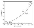
도 20은 오버코트 굴절률의 함수로서 계산된 퍼센트 추출 효율의 선도.
도 21a 내지 도 21c는 광학 구조물을 제조하기 위한 공정의 중간 스테이지 또는 단계에서의 소자의 개략도.
도 22a는 폴리스티렌 입자의 단일 층의 SEM 이미지.
도 22b는 에칭 및 재유동된 도 22a의 입자의 SEM 이미지.
도 22c는 ZnS로 오버코팅된 도 22b의 입자의 SEM 이미지.
도 23은 광원의 개략적인 측면도.
도 24는 오버코트 굴절률의 함수로서 계산된 퍼센트 추출 효율의 선도.
다수의 도면에 사용된 동일한 도면 부호는 동일하거나 유사한 특성 및 기능을 갖는 동일하거나 유사한 요소를 지칭한다.The invention may be more fully understood and appreciated in view of the following detailed description of various embodiments of the invention in conjunction with the accompanying drawings.
1 is a schematic side view of a light emitting system.
2 is a schematic side view of a structured layer and overcoat.
3 is a schematic side view of another structured layer and another overcoat.
4 is a schematic side view of another structured layer and another overcoat.
5A and 5B are scanning electron microscope (SEM) images of a single layer of nanoparticles and multiple layers of nanoparticles, respectively.
6A and 6B are SEM images of an overcoated single layer of nanoparticles and an overcoated multilayer of nanoparticles, respectively.
7 is an SEM image of another overcoated single layer of nanoparticles.
8 is a schematic side view of a light emitting system.
9 is a schematic intensity spectrum of emitted light.
10 is a schematic band diagram of an optical transducer.
11 is a schematic band diagram of another optical transducer.
12 is a schematic band diagram of another optical transducer.
13 is a schematic band diagram of another optical transducer.
14 is a schematic band diagram of another optical transducer.
15 is a schematic band diagram of another optical transducer.
16 is a schematic band diagram of another optical transducer.
17 is a schematic band diagram of another optical transducer.
18 is a schematic side view of an optical structure.
19 is a schematic side view of a light emitting system.
20 is a plot of percent extraction efficiency calculated as a function of overcoat refractive index.
21A-21C are schematic views of a device at an intermediate stage or stage of a process for making an optical structure.
22A is an SEM image of a single layer of polystyrene particles.
FIG. 22B is an SEM image of the particles of FIG. 22A etched and reflowed. FIG.
FIG. 22C is an SEM image of the particles of FIG. 22B overcoated with ZnS. FIG.
23 is a schematic side view of a light source.
24 is a plot of percent extraction efficiency calculated as a function of overcoat refractive index.
Like numbers used in the various drawings refer to the same or similar elements having the same or similar properties and functions.
본 출원은 반도체 광원 및 하나 이상의 파장 변환기(wavelength converter)를 포함하는 반도체 발광 소자를 개시하며, 여기서 변환기는 반도체 파장 변환기일 수 있다. 본 출원은 또한 광 추출을 향상시키기 위한 구조체를 개시한다.The present application discloses a semiconductor light emitting device comprising a semiconductor light source and one or more wavelength converters, where the converter may be a semiconductor wavelength converter. The present application also discloses a structure for improving light extraction.
몇몇 개시된 소자는 III-V 족과 같은 동일한 반도체 족으로부터의 광원과 광 변환 층을 갖는다. 이러한 경우, 예를 들어 III-V LED와 같은 III-V 광원 상에서 직접 III-V 파장 변환기를 모놀리식(monolithically) 성장시키고 제조하는 것이 실현가능할 수 있다. 그러나, 몇몇 경우에, 원하는 출력 파장, 높은 변환 효율 또는 기타 원하는 특성을 갖는 파장 변환기는 LED가 속한 반도체 족과 상이한 반도체 족으로부터의 것일 수 있다. 이러한 경우에는, 고품질로 하나의 구성요소를 다른 구성요소 상에서 성장시키는 것이 가능하지 않을 수 있거나 실현가능하지 않을 수 있다. 예를 들어, 고효율 파장 변환기는 II-VI 족으로부터의 것일 수 있고, LED와 같은 광원은 III-V 족으로부터의 것일 수 있다. 이러한 경우, 광원에 광 변환기를 부착하기 위한 다양한 방법이 채용될 수 있다. 몇몇 이러한 방법은 2007년 12월 10일자로 출원된 미국 특허 출원 제61/012608호에 기술되어 있다.Some disclosed devices have light sources and light conversion layers from the same semiconductor group, such as group III-V. In such a case, it may be feasible to monolithically grow and manufacture a III-V wavelength converter directly on a III-V light source such as, for example, a III-V LED. However, in some cases, the wavelength converter with the desired output wavelength, high conversion efficiency or other desired characteristics may be from a semiconductor group different from the semiconductor group to which the LED belongs. In such a case, it may not be possible or feasible to grow one component on another component with high quality. For example, the high efficiency wavelength converter may be from Group II-VI, and a light source such as an LED may be from Group III-V. In such a case, various methods for attaching the light transducer to the light source can be employed. Some such methods are described in US patent application Ser. No. 61/012608, filed Dec. 10, 2007.
본 출원에 개시된 파장 변환기는 광원에 의해 방출된 광을 하향 변환한다. 본 명세서에서 사용되는 바와 같이, 하향 변환은 변환된 광의 파장이 변환되지 않은 광 또는 입사 광의 파장보다 큰 것을 의미한다.The wavelength converter disclosed in this application down converts light emitted by the light source. As used herein, downconversion means that the wavelength of the converted light is greater than the wavelength of unconverted or incident light.
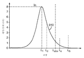
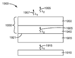
도 19는 광원(1910), 광 변환 층(1920) 및 광 추출 층(1930)을 포함하는 발광 시스템(1900)의 개략적인 측면도이다. 광원(1910)은 전형적으로 UV 또는 청색 스펙트럼 영역의 제1 파장 λ1의 광(1915)을 방출한다. 광 변환 층(1920)은 광(1915)의 적어도 일부를 전형적으로 녹색 또는 적색 스펙트럼 영역의 더 긴 제2 파장 λ2의 광(1925)으로 변환한다. 광 추출 층(1930)은 광 변환 층(1920)으로부터의 광(1925)의 추출을 향상시킴으로써 발광 시스템의 출력 광의 휘도 또는 세기를 개선한다. 예를 들어, 광 추출 층(1930)은, 그렇지 않을 경우 광 변환 층(1920)에 갇히거나 달리 광 변환 층에 의해 투과되지 않을 광을 추출한다.19 is a schematic side view of a
일반적으로, 광 변환 층(1920)은 제1 파장의 광의 적어도 일부를 제2 파장의 광으로 변환할 수 있는 임의의 요소 또는 재료를 포함할 수 있다. 예를 들어, 층(1920)은 인광체, 형광 염료, 콘쥬게이트된(conjugated) 발광 유기 재료, 예컨대 폴리플루오렌, 축광(photoluminescent) 반도체 층, 반도체 포텐셜 웰, 또는 반도체 양자점(quantum dot)들의 어셈블리나 복수의 반도체 양자점을 포함할 수 있다. 광 변환 층(1920)에 사용될 수 있는 예시적인 인광체는 스트론튬 티오갈레이트, 도핑된 GaN, 구리-활성화된 황화아연, 및 은-활성화된 황화아연을 포함한다. 다른 유용한 인광체는 도핑된 YAG, 실리케이트, 옥시질화규소(silicon oxynitride), 질화규소, 및 알루미네이트 기반 인광체를 포함한다. 이러한 인광체의 예는 Ce:YAG, SrSiON:Eu, SrBaSiO:Eu, SrSiN:Eu, 및 BaSrSiN:Eu를 포함한다.In general, light converting
몇몇 경우에, 광 변환 층(1920)은 Ce:YAG 슬래브와 같은 슬래브 인광체를 포함할 수 있다. Ce:YAG 슬래브는, 예를 들어 미국 특허 제7,361,938호에 기술된 바와 같이, 예컨대 상승된 온도 및 압력에서 Ce:YAG 인광체 입자를 소결하여 실질적으로 광학적으로 투명하고 산란이 없는 슬래브를 형성함으로써 제조될 수 있다.In some cases, light converting
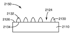
광 추출 층(1930)은 광 변환 층(1920) 상에 직접 배치된 구조화된 층(1940), 및 구조화된 층 상에 배치된 구조화된 오버코트(1950)와 같은 오버코트(1950)를 포함한다. 구조화된 층(1940)은 광 변환 층(1920) 상에 직접 배치된 복수의 구조체를 포함한다. 몇몇 경우에, 오버코트의 외부 표면은 구조화된 층의 외부 표면과 정합한다.
몇몇 경우에, λ2에서의 구조체의 굴절률은 동일한 파장에서의 광 변환 층(1920) 내의 최외측 층의 굴절률보다 낮다. 저굴절률의 구조화된 층(1940)이 광 변환 층의 출력 표면(1921) 상에 형성될 수 있는데, 예를 들어 출력 표면 상에 포토레지스트(photoresist)를 광패터닝(photopatterning)하는 것과 같이 패터닝함으로써, 또는 출력 표면 상에 나노입자와 같은 입자들의 부분적인 또는 완전한 단층(monolayer) 또는 입자들의 다층(multilayer)을 증착함으로써 형성될 수 있다. 몇몇 경우에, 구조화된 층은, 예를 들어 λ2에서의 구조화된 층의 굴절률을 낮추기 위해 공기를 포함할 수 있다. 예를 들어, 몇몇 경우에, 구조화된 층은 출력 표면(1921) 상에 중공형(hollow) 구조체 또는 입자를 포함할 수 있다. 공기 또는 공기 포켓을 포함하는 구조화된 층(1940)은, 예를 들어 출력 표면 상에 유기 재료와 같은 재료를 패터닝하고, 패터닝된 재료를 오버코트로 오버코팅하고, 예를 들어 상승된 온도에서 오버코팅된 패터닝된 재료의 일부를 분해함으로써 공기 영역을 형성하도록 이러한 오버코팅된 패터닝된 재료의 일부를 제거함으로써, 출력 표면 상에 형성될 수 있다. 몇몇 경우에, 구조화된 층(1940) 내의 구조체의 굴절률은 구조화된 층에 바로 인접해 있는 광 변환 층(1920) 내의 최외측 층의 굴절률보다 작다.In some cases, the refractive index of the structure at λ 2 is lower than the refractive index of the outermost layer in
오버코트(1950)는 광 변환 층(1920)으로부터의 광의 추출을 향상시킨다. 몇몇 경우에, 오버코트는 유리질(glassy) 재료 또는 금속 산화물, 예컨대 Al2O3, TiO2, ZrO2, La2O3, Ta2O5, HfO2, 실리케이트, 질화규소, 옥시질화규소, 또는 산화인듐주석을 포함할 수 있다. 몇몇 경우에, 오버코트는 ZnS, ZnSe, ZnO 또는 반도체 합금, 예컨대 ZnSxSe1 -x를 함유하는 오버코트와 같은 반도체 오버코트일 수 있다. 몇몇 경우에, 오버코트는 졸-겔(sol-gel), 예컨대 치밀화된(densified) 졸-겔일 수 있다. 몇몇 경우에, 오버코트의 굴절률은 구조화된 층에 바로 인접해 있는 광 변환 층(1920) 내의 최외측 층의 굴절률보다 크다.
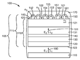
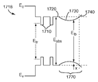
도 1은 광자 에너지 E1을 갖는 제1 파장 λ1의 광을 방출하는 전계발광 소자(electroluminescent device)(110), 및 제1 파장의 광의 적어도 일부를 광자 에너지 E2를 갖는 더 긴 제2 파장 λ2의 광으로 변환하기 위한 반도체 광 변환 구조물(115)을 포함하는 반도체 발광 요소(105)의 개략적인 측면도이다.1 shows an
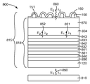
반도체 광 변환 구조물(115)은 전계발광 소자(110)를 향한 제1 윈도우(120), 제1 윈도우 상에 배치된 제1 흡수 층(130), 제1 흡수 층 상에 배치된 포텐셜 웰(140), 포텐셜 웰 상에 배치된 제2 흡수 층(131), 제2 흡수 층 상에 배치된 제2 윈도우(121), 제2 윈도우 상에 직접 배치된 구조화된 층(150), 구조화된 층 상에 배치된 오버코트(160), 및 오버코트 상에 배치되며 반도체 전계발광 요소(105)를 봉지하는 봉지재(170)를 포함한다.The semiconductor
일반적으로, 광 변환기(118)는 제1 파장 λ1의 광의 적어도 일부를 제2 파장 λ2의 광으로 변환할 수 있는 임의의 요소를 포함할 수 있다. 예를 들어, 광 변환기(118)는 인광체, 형광 염료, 콘쥬게이트된 발광 유기 재료, 예컨대 폴리플루오렌을 포함할 수 있다. 광 변환기(118)에 사용될 수 있는 예시적인 인광체는 스트론튬 티오갈레이트, 도핑된 GaN, 구리-활성화된 황화아연, 및 은-활성화된 황화아연을 포함한다.In general, the
몇몇 경우에, 층(140)은 포텐셜 웰, 양자 웰, 양자점, 또는 이들 각각의 다수 또는 복수를 포함할 수 있다. 무기 포텐셜 및 양자 웰, 예컨대 무기 반도체 포텐셜 및 양자 웰은 전형적으로, 예를 들어 유기 재료와 비교하여 증가된 광 변환 효율을 가지며, 수분과 같은 환경 요소에 덜 민감하여 신뢰성이 보다 높다. 또한, 무기 포텐셜 및 양자 웰은 더 좁은 출력 스펙트럼을 갖는 경향이 있으며, 그 결과 예를 들어 색역(color gamut)이 개선된다.In some cases,
본 명세서에 사용되는 바와 같이, 포텐셜 웰은 한 차원에서만 캐리어(carrier)를 구속하도록 설계된 다층 반도체 구조의 반도체 층(들)을 의미하며, 여기서 반도체 층(들)은 주변 층보다 낮은 전도대 에너지(conduction band energy) 및/또는 주변 층보다 높은 가전자대 에너지(valence band energy)를 갖는다. 양자 웰은 일반적으로 양자화 효과가 웰에서의 전자-정공 쌍 재결합을 위한 에너지를 증가시키기에 충분히 얇은 포텐셜 웰을 의미한다. 양자 웰은 전형적으로 약 100 ㎚ 이하, 또는 약 10 ㎚ 이하의 두께를 갖는다. 양자점은 전형적으로 약 100 ㎚ 이하, 또는 약 10 ㎚ 이하의 최대 치수를 갖는다.As used herein, a potential well refers to a semiconductor layer (s) of a multi-layered semiconductor structure designed to confine a carrier only in one dimension, where the semiconductor layer (s) has lower conduction band energy than the surrounding layer. band energy and / or higher valence band energy than the surrounding layer. A quantum well generally refers to a potential well where the quantization effect is thin enough to increase the energy for electron-hole pair recombination in the well. Quantum wells typically have a thickness of about 100 nm or less, or about 10 nm or less. Quantum dots typically have a maximum dimension of about 100 nm or less, or about 10 nm or less.
몇몇 경우에, 포텐셜 또는 양자 웰(140)은 전계발광 소자(110)에 의해 방출된 광자의 에너지 E1보다 작은 전이 에너지 Epw를 갖는 II-VI 반도체 포텐셜 또는 양자 웰을 포함한다. 일반적으로, 포텐셜 또는 양자 웰(140)의 전이 에너지는 포텐셜 또는 양자 웰에 의해 재방출되는 광자의 에너지 E2와 실질적으로 동일하다.In some cases, potential or
몇몇 경우에, 포텐셜 웰(140)은 합금의 3가지 구성성분으로서 화합물 ZnSe, CdSe, 및 MgSe를 갖는 CdMgZnSe 합금을 포함할 수 있다. 몇몇 경우에, Cd, Mg, 및 Zn 중 하나 이상, 특히 Mg가 합금에 없을 수 있다. 예를 들어, 포텐셜 웰(140)은 적색으로 재방출할 수 있는 Cd0.70Zn0.30Se 양자 웰, 또는 녹색으로 재방출할 수 있는 Cd0.33Zn0.67Se 양자 웰을 포함할 수 있다. 다른 예로서, 포텐셜 웰(140)은 Cd, Zn, Se, 및 선택적으로 Mg의 합금을 포함할 수 있고, Mg의 경우에 합금 시스템은 Cd(Mg)ZnSe로 나타낼 수 있다. 또 다른 예로서, 포텐셜 웰(140)은 Cd, Mg, Se, 및 선택적으로 Zn의 합금을 포함할 수 있다. 몇몇 경우에, 포텐셜 웰은 ZnSeTe를 포함할 수 있다. 몇몇 경우에, 양자 웰(140)은 약 1 ㎚ 내지 약 100 ㎚, 또는 약 2 ㎚ 내지 약 35 ㎚ 범위의 두께를 갖는다.In some cases,
일반적으로, 포텐셜 웰(140)은 임의의 전도대 및/또는 가전자대 프로파일을 가질 수 있다. 예시적인 프로파일은, 예를 들어 미국 특허 출원 제60/893804호에 기술되어 있다.In general,
몇몇 경우에, 포텐셜 웰(140)은 n-도핑 또는 p-도핑될 수 있으며, 여기서 도핑은 임의의 적합한 방법에 의해 그리고 임의의 적합한 도펀트의 포함에 의해 달성될 수 있다. 몇몇 경우에, 전계발광 소자(110) 및 포텐셜 웰(140)은 2개의 상이한 반도체 족으로부터의 것일 수 있다. 예를 들어, 그러한 경우, 전계발광 소자(110)는 III-V 반도체 소자일 수 있으며, 포텐셜 웰(140)은 II-VI 포텐셜 웰일 수 있다. 몇몇 경우에, 전계발광 소자(110)는 AlGaInN 반도체 합금을 포함할 수 있고, 포텐셜 웰(140)은 Cd(Mg)ZnSe 반도체 합금을 포함할 수 있으며, 괄호 안에 포함된 재료는 선택적 재료이다.In some cases,
일반적으로, 반도체 광 변환 구조물(115)은 하나 이상의 포텐셜 웰을 가질 수 있다. 몇몇 경우에, 구조물(115)은 다수의 포텐셜 웰을 가질 수 있다. 예를 들어, 그러한 경우, 구조물(115)은 적어도 2개의 포텐셜 웰, 또는 적어도 5개의 포텐셜 웰, 또는 적어도 10개의 포텐셜 웰을 가질 수 있다. 몇몇 경우에, 구조물(115)은 상이한 전이 에너지를 갖는, 적어도 2개의 포텐셜 웰, 또는 적어도 3개의 포텐셜 웰, 또는 적어도 4개의 포텐셜 웰을 가질 수 있다.In general, the semiconductor
몇몇 경우에, 포텐셜 웰(140)은 실질적으로 제1 파장 λ1의 광을 흡수한다. 예를 들어, 그러한 경우에, 포텐셜 웰(140)은 제1 파장 λ1의 광의 적어도 30%, 또는 적어도 40%, 또는 적어도 50%를 흡수한다. 몇몇 경우에, 포텐셜 웰(140)은 실질적으로 제1 파장 λ1에서 광학적으로 투과성이다. 예를 들어, 그러한 경우에, 포텐셜 웰(140)은 제1 파장 λ1의 광의 적어도 60%, 또는 적어도 70%, 또는 적어도 80%, 또는 적어도 90%를 투과시킨다.In some cases,
광 흡수 층(130, 131)은 반도체 광 변환 구조물(115)에서 광(180)의 흡수 및 캐리어의 생성을 보조한다. 몇몇 경우에, 광 흡수 층(130, 131)은 광(180)의 적어도 일부를 흡수하고, 그 결과 전자-정공 캐리어와 같은 광-생성 캐리어(photo-generated carrier) 쌍을 생성한다. 캐리어는 광 흡수 층으로부터 포텐셜 웰(140)로 확산하거나 이동하며, 여기서 이들은 재결합하여 제2 파장 λ2의 광을 방출한다.The
광 흡수 층(130, 131)은 캐리어의 재결합 및 제2 파장 λ2의 광의 방출을 위해 광-생성 캐리어가 포텐셜 웰로 효율적으로 확산할 수 있도록 포텐셜 웰에 근접하게 배치된다.The
몇몇 경우에, 반도체 광 변환 구조물(115) 내의 광 흡수 층은 포텐셜 웰(140)에 바로 인접해 있을 수 있으며, 이는 흡수 층과 포텐셜 웰 사이에 어떠한 개재 층도 배치되지 않음을 의미한다. 예를 들어, 도 1에서, 각각의 제1 및 제2 광 흡수 층(130, 131)은 포텐셜 웰(140)에 바로 인접해 있다. 몇몇 경우에, 반도체 광 변환 구조물(115) 내의 광 흡수 층은 포텐셜 웰(140)에 가깝게 인접해 있을 수 있으며, 이는 하나 또는 몇 개의 개재 층이 흡수 층과 포텐셜 웰 사이에 배치될 수 있음을 의미한다. 예를 들어, 몇몇 경우에, 도 1에 도시되지 않은 하나 이상의 개재 층이 제1 광 흡수 층(130)과 포텐셜 웰(140) 사이에 배치될 수 있다.In some cases, the light absorbing layer in the semiconductor
몇몇 경우에, 광 흡수 층은 무기 반도체, 예컨대 II-VI 반도체와 같은 반도체를 포함할 수 있다. 예를 들어, 하나 이상의 흡수 층(130, 131)은 Cd(Mg)ZnSe 반도체 합금을 포함할 수 있다.In some cases, the light absorbing layer can include an inorganic semiconductor, such as a semiconductor such as II-VI semiconductor. For example, the one or more
몇몇 경우에, 광 흡수 층은 전계발광 소자(110)에 의해 방출된 광자의 에너지 E1보다 작은 밴드 갭 에너지 Eabs를 갖는다. 이러한 경우에, 광 흡수 층은 전계발광 소자에 의해 방출되는 광을 흡수할 수 있는데, 예를 들어 강하게 흡수할 수 있다. 몇몇 경우에, 광 흡수 층은 포텐셜 웰(140)의 전이 에너지보다 큰 밴드 갭 에너지를 갖는다. 이러한 경우에, 광 흡수 층은 제2 파장 λ2에서 포텐셜 웰에 의해 재방출되는 광(181)에 대해 실질적으로 광학적으로 투명하다.In some cases, the light absorbing layer has a band gap energy E abs less than the energy E 1 of photons emitted by the
몇몇 경우에, 제2 광 흡수 층(131)과 같은 광 흡수 층은 제2 파장 λ2에서 방출된 광(181)의 광자 에너지보다 작은 밴드 갭 에너지를 갖는다. 이러한 경우에, 광 흡수 층은 광(181)의 적어도 일부를 흡수할 수 있다. 이러한 경우에, 흡수된 광의 적어도 일부는 더 긴 제3 파장 λ3의 광으로 하향 변환될 수 있다.In some cases, the light absorbing layer, such as the second
몇몇 경우에, 반도체 광 변환 구조물(115) 내의 적어도 하나의 광 흡수 층은 도펀트로 도핑된다. 광 흡수 층이 Cd(Mg)ZnSe 합금을 포함할 때와 같은 몇몇 경우에, 도펀트는 VII 족 n형 도펀트일 수 있다. 몇몇 경우에, 도펀트는 염소 또는 요오드를 포함할 수 있다. 몇몇 경우에, 도펀트의 수 밀도(number density)는 약 1017 ㎝-3 내지 약 1018 ㎝-3 범위이다. 다른 예시적인 도펀트는 Al, Ga, In, F, Br, I, 및 N을 포함한다.In some cases, at least one light absorbing layer in semiconductor
예시적인 반도체 광 변환 구조물(115)은 2개의 광 흡수 층(130, 131)을 포함한다. 일반적으로, 반도체 광 변환 구조물은 흡수 층을 전혀 갖지 않거나, 하나, 둘, 또는 둘 초과로 가질 수 있다. 몇몇 경우에, 반도체 광 변환 구조물(115)은 상이한 밴드 갭 에너지를 갖는, 적어도 2개, 또는 적어도 3개, 또는 적어도 4개의 광 흡수 층을 가질 수 있다.Exemplary semiconductor
일반적으로, 광 흡수 층은 대응하는 포텐셜 웰에 충분히 가깝게 있어서, 광 흡수 층 내의 광-생성 캐리어는 포텐셜 웰로 확산할 적절한 기회를 갖는다. 반도체 다층 스택이 광 흡수 층을 포함하지 않는 경우에, 포텐셜 웰(들)은 실질적으로 제1 파장 λ1의 광을 흡수할 수 있다.In general, the light absorbing layer is close enough to the corresponding potential well so that the light-generating carrier in the light absorbing layer has a suitable opportunity to diffuse into the potential well. If the semiconductor multilayer stack does not include a light absorbing layer, the potential well (s) can substantially absorb light of the first wavelength λ 1 .
제1 및 제2 윈도우(120, 121)는 주로, 흡수 층 및/또는 포텐셜 웰에서 광-생성되는 전자-정공 쌍과 같은 캐리어가 구조물(115)의 자유 또는 외부 표면으로 이동할 기회가 전혀 없거나 아주 적도록 하는 배리어(barrier)를 제공하도록 설계된다. 예를 들어, 제1 윈도우(120)는 주로 제1 흡수 층(130) 내에 생성된 캐리어가, 이들이 비-방사성으로(non-radiatively) 재결합할 수 있는 표면(123)으로 이동하는 것을 방지하도록 설계된다. 몇몇 경우에, 윈도우(120, 121)는 전계발광 소자(110)에 의해 방출된 광자의 에너지 E1보다 큰 밴드 갭 에너지 Ew를 갖는다. 이러한 경우에, 윈도우(120, 121)는 전계발광 소자(110)에 의해 방출된 광 및 포텐셜 웰(140)에 의해 재방출된 광에 대해 실질적으로 광학적으로 투명하다.The first and
예시적인 반도체 광 변환 구조물(115)은 2개의 윈도우를 포함한다. 일반적으로, 광 변환 구조물은 윈도우를 전혀 갖지 않거나, 하나 또는 두 개를 가질 수 있다. 예를 들어, 몇몇 경우에, 반도체 광 변환 구조물(115)은 전계발광 소자(110)와 포텐셜 웰(140) 사이 또는 전계발광 소자(110)와 흡수 층(130) 사이에 배치된 단일 윈도우를 가질 수 있다.Exemplary semiconductor
몇몇 경우에, 반도체 광 변환 구조물(115) 내의 2개의 인접한 층들 사이의 계면의 위치는 명확하거나 뚜렷한 계면일 수 있다. 층 내의 재료 조성이 두께 방향에 따른 거리의 함수로서 변할 때와 같은 몇몇 경우에, 2개의 인접한 층들 사이의 계면은 명확하지 않을 수 있으며, 예를 들어 구배형(graded) 영역을 한정하는 구배형 계면일 수 있다. 예를 들어, 몇몇 경우에, 제1 흡수 층(130) 및 제1 윈도우(120)는 동일한 재료 성분을 갖지만 상이한 재료 농도를 가질 수 있다. 이러한 경우에, 흡수 층의 재료 조성은 윈도우 층의 재료 조성으로 점차적으로 변할 수 있어서, 2개 층들 사이의 구배형 계면 또는 영역이 될 수 있다. 예를 들어, 두 층 모두가 Mg를 포함하는 경우, Mg의 농도는 흡수 층에서 윈도우로 점차 이동함에 따라 증가될 수 있다.In some cases, the location of the interface between two adjacent layers in the semiconductor
제2 윈도우(121)는 파장 λ2를 포함하는 관심 파장 영역에서 굴절률 n1을 갖는다. 몇몇 경우에, λ1은 UV 또는 청색 파장이고, λ2는 약 420 ㎚ 내지 약 650 ㎚ 범위의 가시 파장이다. 이러한 경우에, n1은 스펙트럼의 가시 영역의 굴절률일 수 있다. 몇몇 경우에, n1은 파장 λ2 또는 그 부근에서의 굴절률이다.The
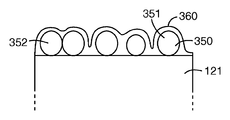
예시적인 반도체 광 변환 구조물(115)에서, 제2 윈도우(121)는 포텐셜 웰(140) 상에 배치되며, 반도체 광 변환 구조물의 외부 층(121) 및 광 변환기(118)의 최외측 층을 형성한다. 구조화된 층(150)은, 예를 들어 λ2에서 굴절률 n2를 가지며, 외부 층 또는 제2 윈도우(121) 상에 직접 배치된다. 굴절률 n2는 제2 윈도우(121)의 굴절률 n1보다 작다. 몇몇 경우에, n1과 n2 사이의 차이는 적어도 0.2, 또는 적어도 0.3, 또는 적어도 0.4, 또는 적어도 0.5, 또는 적어도 0.6, 또는 적어도 0.7, 또는 적어도 0.8, 또는 적어도 0.9이다.In the exemplary semiconductor
구조화된 층(150)은 구조체(151 내지 154)와 같은 복수의 구조체를 포함한다. 복수의 구조체 중 일부 구조체는 구조체(151, 152)와 같이 이산되어 있을 수 있다. 일부 구조체는 베이스(155)를 통해 서로 연결되어 있는 구조체(153, 154)와 같이 베이스를 통해 연결될 수 있다. 구조화된 층(150)은 제2 윈도우(121)를 노출시키는 개방부(101, 102)와 같은 복수의 개방부를 포함한다.
몇몇 경우에, 구조화된 층(150)은 실질적으로 제2 파장 λ2에서 광학적으로 투명하다. 예를 들어, 그러한 경우, 파장 λ2에서의 구조화된 층의 총 광학 투과율은 적어도 50%, 또는 적어도 60%, 또는 적어도 70%, 또는 적어도 80%이다.In some cases, structured
몇몇 경우에, 구조화된 층(150) 내의 복수의 구조체는 구조체들의 규칙적인 어레이를 형성한다. 몇몇 경우에, 구조체들은 제2 윈도우(121)의 상부 표면(125)에 걸쳐 랜덤으로 배치된다. 몇몇 경우에, 구조화된 층(150)은, 예를 들어 와플(waffle) 패턴과 유사하게 구조체들 중 적어도 일부 사이에 개방부를 갖는 상태로 연결되어 있는 복수의 구조체 또는 구조체들의 어레이를 포함하는 연속적인 층이다.In some cases, the plurality of structures in
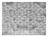
몇몇 경우에, 구조화된 층(150) 내의 복수의 구조체는 복수의 이산된 구조체를 형성한다. 예를 들어, 몇몇 경우에, 구조화된 층은 복수의 입자를 포함할 수 있다. 예를 들어, 도 3의 구조화된 층(350)은 입자(351, 352)와 같은 복수의 입자를 갖는다. 몇몇 경우에, 입자는 실질적으로 마이크로입자 또는 나노입자이다. 예를 들어, 그러한 경우에, 입자의 평균 크기는 2000 ㎚ 이하, 또는 1500 ㎚이하, 또는 1000 ㎚ 이하, 또는 750 ㎚ 이하이다. 구조화된 층(350) 내의 입자들은 임의의 규칙적이거나 불규칙적인 형상과 같은 임의의 형상을 가질 수 있다.In some cases, the plurality of structures in
몇몇 경우에, 도 1의 구조화된 층(150)은 입자들의 상당한 분율이 실질적으로 구형인 복수의 입자를 포함한다. 예를 들어, 그러한 경우에, 입자의 최소 치수에 대한 최대 치수의 비는 1.3 이하, 또는 1.25 이하, 또는 1.2 이하, 또는 1.15 이하, 또는 1.1 이하이다.In some cases, structured
몇몇 경우에, 구조화된 층(150)은 패터닝가능한 또는 광패터닝가능한 유기 재료 또는 중합체, 예컨대 포토레지스트와 같은 유기 재료를 포함할 수 있다. 몇몇 경우에, 구조화된 층(150)은 폴리스티렌, 예컨대 폴리스티렌 미소구체(microsphere)를 포함할 수 있다. 몇몇 경우에, 구조화된 층(150)은 무기 재료, 예컨대 금속 산화물 또는 유리를 포함할 수 있다. 무기 재료의 예는 SiO2, GeO2, Al2O3, MgF2, 및 실리케이트 유리를 포함한다.In some cases, structured
몇몇 경우에, 구조화된 층(150)은 상부 표면(125)에 걸쳐 조밀하게 패킹된(closely packed) 단일 구조체 또는 구조체들의 단층을 포함할 수 있다. 몇몇 경우에, 구조화된 층(150)은 구조체들의 서브-단층(sub-monolayer)을 포함할 수 있으며, 이는 구조체들이 조밀하게 패킹되지 않고, 그리고/또는 구조체를 전혀 포함하지 않거나 아주 적게 포함하는, 구조체의 공칭 또는 평균 크기보다 상당히 큰 영역이 있음을 의미한다. 이러한 경우에, 서브-단층 구조화된 층(150)의 개방 영역은 단일 입자와 같은 단일 구조체의 평균 크기보다 상당히 클 수 있다.In some cases, structured
몇몇 경우에, 구조화된 층(150)은 구조체들의 다층을 포함할 수 있다. 예를 들어, 도 4는 입자들(451)의 다층을 포함하는, 제2 윈도우(121) 상에 직접 배치된 구조화된 층(450)의 개략적인 측면도이다. 구조화된 층은 연속적인 오버코트(460)로 코팅되고, 봉지재(470)가 오버코트를 덮는다.In some cases, structured
구조화된 오버코트(160)는 적어도 구조화된 층(150)의 일부분 및 구조화된 층(150) 내의 개방부를 통해 윈도우가 노출되어 있는 영역 내의 제2 윈도우(121)의 일부분 상에 직접 배치된다. 오버코트(160)는, 예를 들어 제2 굴절률 n2보다 큰 파장 λ2에서의 제3 굴절률 n3를 갖는다. 몇몇 경우에, n3는 n1보다 작다. 몇몇 경우에, n3는 n1보다 크다. 몇몇 경우에, n3와 n2 사이의 차이는 적어도, 0.2, 또는 적어도 0.3, 또는 적어도 0.4, 또는 적어도 0.5, 또는 적어도 0.6, 또는 적어도 0.7 또는 적어도 0.8, 또는 적어도 0.9이다.
몇몇 경우에, 오버코트(160)는, 그렇지 않을 경우 제2 윈도우의 표면(125)에서 내부 전반사될 광(181)을 추출할 수 있다. 이러한 경우에, 오버코트는 반도체 광 변환 구조물(115)로부터의 제2 파장 λ2의 광(181)의 추출을 향상시킨다.In some cases,
몇몇 경우에, 구조화된 오버코트(160)의 외부 표면(162)은 구조화된 층(150)의 외부 표면(161)과 실질적으로 정합한다. 예를 들어, 몇몇 경우에, 오버코트(160)는 진공 증착 기술을 사용하여 구조화된 층(150) 상에 배치될 수 있다. 이러한 경우에, 외부 표면(162)은 외부 표면(161)과 정합할 수 있다. 몇몇 경우에, 구조화된 오버코트의 평균 두께는 구조화된 층(150) 내의 구조체의 평균 크기보다 크지 않다. 몇몇 경우에, 오버코트(160)의 평균 두께는 1000 ㎚ 이하, 또는 800 ㎚ 이하, 또는 700 ㎚ 이하, 또는 600 ㎚ 이하, 또는 500 ㎚ 이하, 또는 400 ㎚ 이하이다.In some cases, the
몇몇 경우에, 오버코트(160)는 실질적으로 제2 파장 λ2에서 광학적으로 투명하다. 예를 들어, 그러한 경우에, 파장 λ2에서의 오버코트의 총 광학 투과율은 적어도 50%, 또는 적어도 60%, 또는 적어도 70%, 또는 적어도 80%이다.In some cases,
몇몇 경우에, 오버코트(160)는, 예를 들어 하나 이상의 섬(island)을 포함함으로써, 불연속적인 층일 수 있다. 예를 들어, 도 2에서, 구조화된 층(250)은 제2 윈도우(121) 상에 직접 배치되고, 구조체(251, 252)들 사이에 개방부(255)를 한정한다. 오버코트(260)는 구조화된 층(250) 상에 그리고 개방 영역에서는 제2 윈도우(121) 상에 직접 배치되어, 개방 및 노출된 영역(255) 내에 섬(261)을 형성한다. 몇몇 경우에, 오버코트(160)는 연속적인 층일 수 있다. 예를 들어, 도 3에서, 구조화된 층(350) 상에 직접 배치된 오버코트(360)는 연속적인 층을 형성한다.In some cases,
몇몇 경우에, 오버코트(160)는 반도체, 금속 산화물, 또는 세라믹을 포함할 수 있다. 몇몇 경우에, 오버코트는 Si3N4, 옥시질화규소, 실리케이트, ZnS, ZnSe, ZnTe, ZnSSe, ZnSeTe, ZnSTe, CdS, CdSe, CdSSe, ITO, TiO2, ZrO2, Ta2O5, 및 HfO2 중 적어도 하나를 포함할 수 있다.In some cases,
봉지재(170)는 오버코트(160) 상에 배치되어, 반도체 발광 요소(105)를 봉지하며, 요소를 예를 들어 환경의 수분으로부터 보호한다. 몇몇 경우에, 봉지재는, 예를 들어 광(181)이 반도체 발광 요소를 빠져나갈 때 이 광을 시준하기 위한 광학 파워(optical power)와 같은 광학 기능을 가질 수 있다.
전계발광 소자(110)는 전기 신호에 응답하여 광을 방출할 수 있는 임의의 소자일 수 있다. 예를 들어, 전계발광 소자는 전류에 응답하여 광자를 방출할 수 있는 발광 다이오드(LED) 또는 레이저 다이오드일 수 있다. LED 전계발광 소자(110)는 소정 응용에서 바람직할 수 있는 임의의 파장의 광을 방출할 수 있다. 예를 들어, LED는 UV 파장, 가시 파장, 또는 IR 파장의 광을 방출할 수 있다. 몇몇 경우에, LED는 UV 광자를 방출할 수 있는 단파장 LED일 수 있다. 일반적으로, LED는 유기 반도체 또는 무기 반도체 - IV 족 원소, 예컨대 Si 또는 Ge; III-V 화합물, 예컨대 InAs, AlAs, GaAs, InP, AlP, GaP, InSb, AlSb, GaSb, GaN, AlN, InN 및 III-V 화합물의 합금, 예컨대 AlGaInP 및 AlGaInN; II-VI 화합물, 예컨대 ZnSe, CdSe, BeSe, MgSe, ZnTe, CdTe, BeTe, MgTe, ZnS, CdS, BeS, MgS 및 II-VI 화합물의 합금, 또는 상기 열거한 임의의 화합물들의 합금을 포함함 - 와 같은 임의의 적합한 재료로 구성될 수 있다.The
몇몇 경우에, 전계발광 소자(110)는 하나 이상의 p형 및/또는 n형 반도체 층, 하나 이상의 포텐셜 및/또는 양자 웰을 포함할 수 있는 하나 이상의 활성 층, 버퍼 층, 기판 층, 및 덮개 층(superstrate layer)을 포함할 수 있다. 몇몇 경우에, 전계발광 소자(110)는 III-V LED와 같은 III-V 반도체 광원일 수 있고, AlGaInN 반도체 합금을 포함할 수 있다. 예를 들어, 전계발광 소자(110)는 GaN 기반 LED일 수 있다. 다른 예로서, 전계발광 소자(110)는 ZnO 기반 LED와 같은 II-VI LED일 수 있다.In some cases,
개시된 구성들의 이점들 중 일부는 하기의 실시예에 의해 추가로 예시된다. 이러한 실시예에 언급된 특정 재료, 양 및 치수뿐만 아니라 다른 조건 및 상세 사항은 본 발명을 과도하게 제한하는 것으로 해석되어서는 안 된다.Some of the advantages of the disclosed configurations are further illustrated by the following examples. The specific materials, amounts and dimensions mentioned in these examples, as well as other conditions and details, should not be construed as overly limiting the present invention.
실시예 1:Example 1:
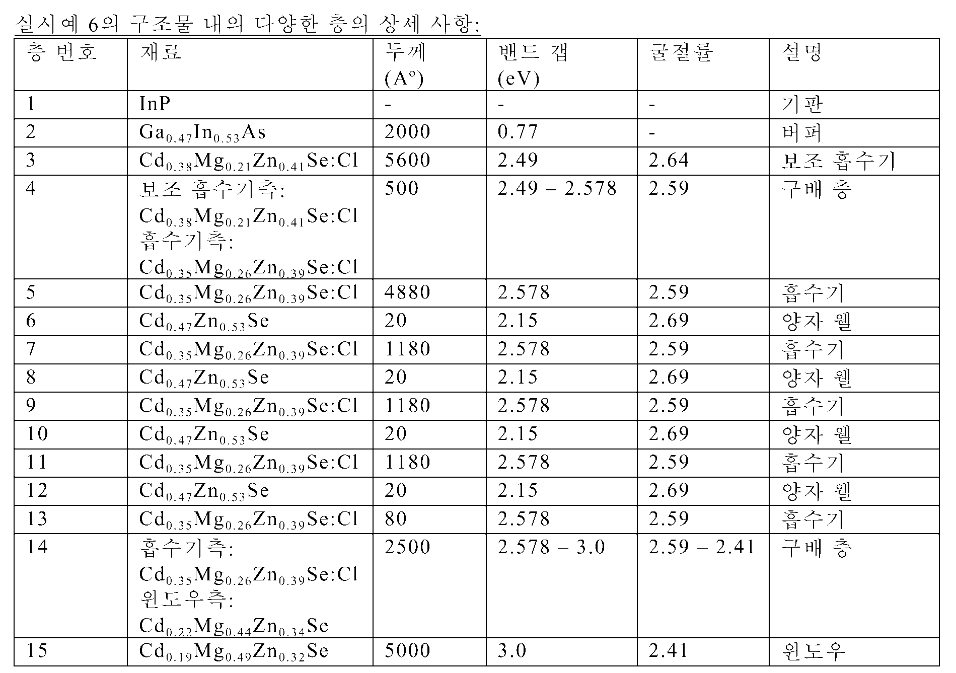
도 1의 광 변환기(118)와 유사한 반도체 광 변환 구조물을 제조하였다. 여러 층들에 대한 상대적인 층 순서와 재료 조성 및 두께의 추정 값이 표 I에 요약되어 있다.A semiconductor light conversion structure similar to the
[표 I]TABLE I

II-VI 성장을 위한 표면을 제조하기 위해 먼저 GaInAs 버퍼 층을 분자 빔 에피텍시(molecular beam epitaxy, MBE)에 의해 InP 기판 상에 성장시켰다. 그 다음, 광 변환을 위한 II-VI 에피텍셜 층(epitaxial layer)의 성장을 위해 구조물을 초-고진공 전사 시스템(ultra-high vacuum transfer system)을 통해 다른 MBE 챔버로 이동시켰다. 변환기(118)는 4개의 CdZnSe 양자 웰(140)을 포함하였다. 각각의 양자 웰(140)을 GaInN 기반 레이저 다이오드에 의해 방출된 440 ㎚의 청색 광을 흡수할 수 있는 CdMgZnSe 흡수 층(130, 131)들 사이에 개재시켰다.To prepare a surface for II-VI growth, a GaInAs buffer layer was first grown on InP substrates by molecular beam epitaxy (MBE). The structure was then moved to another MBE chamber via an ultra-high vacuum transfer system for growth of the II-VI epitaxial layer for light conversion.
구조물을 유리 현미경 슬라이드에 접착식으로 부착시킨 후에 3HCl:1H2O 용액을 이용해 InP 기판을 제거하였다. 에칭제는 GaInAs 버퍼 층(층 #2)에서 정지하였다. 그 후, 버퍼 층을 30 ml 수산화암모늄(30 중량%), 5 ml 과산화수소(30 중량%), 40g 아디프산, 및 200 ml 물의 교반된 용액 내에서 제거하여, 현미경 슬라이드에 부착된 II-VI 광 변환기(118)만을 남겨 두었다.After the structures were adhesively attached to glass microscope slides, the InP substrate was removed using a 3HCl: 1H 2 O solution. The etchant was stopped in the GaInAs buffer layer (layer # 2). The buffer layer is then removed in a stirred solution of 30 ml ammonium hydroxide (30 wt.%), 5 ml hydrogen peroxide (30 wt.%), 40 g adipic acid, and 200 ml water, to attach to the microscope slide II-VI. Only the
실시예 2:Example 2:
실시예 1에서 제조한 구조물의 외부 양자 효율(external quantum efficiency, EQE)을, 이 구조물이 λin = 440 ㎚에서 청색 광을 방출하는 레이저 다이오드에 의해 구조물의 윈도우측으로부터 조명될 때 계산하였다. 측정된 재방출된 파장은 λout = 539 ㎚였다. 식 (Pout/Pin) × (λin/λout)으로부터 EQE를 계산하였으며, 여기서 Pin은 입사 파워였고, Pout은 구조물에서 출사하는 변환된 광의 출력 파워였다. 계산된 EQE는 23%였다.The external quantum efficiency (EQE) of the structure prepared in Example 1 was calculated when the structure was illuminated from the window side of the structure by a laser diode emitting blue light at λ in = 440 nm. The measured re-emitted wavelength was λ out = 539 nm. EQE was calculated from the equation (P out / P in ) × (λ in / λ out ), where P in was the incident power and P out was the output power of the converted light exiting the structure. The calculated EQE was 23%.
실시예 3:Example 3:
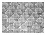
실시예 1에서 제조한 구조물의 흡수기측을 SiO2 나노입자로 코팅하여, 구조화된 층(150)과 유사한 구조화된 층으로 형성하였다. 입자는 약 440 ㎚의 평균 직경을 가졌으며, 닛산 케미칼 아메리카 코포레이션(Nissan Chemical America Corporation)(미국 텍사스주 휴스턴)으로부터 입수하였다. 입자를 5 중량% 고형물 함량으로 1-메톡시-2-프로판올 중에 분산시켰다. 딥 코팅(dip coating) 방법을 사용하여 약 65 ㎜/분의 속도로 용액을 구조물 상에 코팅하였다. 하나의 이러한 샘플(샘플 A)을 단일 회 딥 코팅하였다. 두 번째 이러한 샘플(샘플 B)은 다수 회 딥 코팅하였다. 도 5a 및 도 5b는 각각 샘플 A 및 샘플 B의 측면 주사 전자 현미경(scanning electron microscope, SEM) 이미지이다. 실시예 2에 약술한 방법을 사용하면, 샘플 A 및 샘플 B의 EQE는 각각 30.7% 및 38.2%로 계산되었다.The absorber side of the structure prepared in Example 1 was coated with SiO 2 nanoparticles to form a structured layer similar to
실시예 4:Example 4:
실시예 3으로부터의 샘플 A 및 샘플 B를 플라즈마 화학 기상 증착(plasma enhanced chemical vapor deposition, PECVD) 공정을 사용해 Si3N4 오버코트로 코팅하여, 각각 오버코팅된 샘플 A1 및 샘플 B1을 형성하였다. 오버코트의 두께는 약 300 ㎚였고, Si3N4의 굴절률은 약 1.8이었다. 도 6a 및 도 6b는 각각 오버코팅된 샘플 A1 및 샘플 B1의 측면 SEM 이미지이다. 실시예 2에 약술한 방법을 사용하면, 샘플 A1 및 샘플 B1의 EQE는 각각 41.2% 및 41.5%로 계산되었다. 단일-딥 입자 코팅된 샘플의 경우, Si3N4 오버코트의 추가는 EQE를 30.7%에서 41.2%로 증가시켰으며, 이는 약 34%의 증가이다. 다중-딥 입자 코팅된 샘플의 경우, Si3N4 오버코트의 추가는 EQE를 38.2%에서 41.5%로 증가시켰으며, 이는 약 8.6%의 증가이다.Sample A and Sample B from Example 3 were coated with Si 3 N 4 overcoat using a plasma enhanced chemical vapor deposition (PECVD) process to form overcoated Sample A 1 and Sample B 1 , respectively. . The thickness of the overcoat was about 300 nm and the refractive index of Si 3 N 4 was about 1.8. 6A and 6B are side SEM images of Sample A 1 and Sample B 1 overcoated, respectively. Using the method outlined in Example 2, the EQE of Sample A 1 and Sample B 1 was calculated to be 41.2% and 41.5%, respectively. For single-dip particle coated samples, the addition of Si 3 N 4 overcoat increased the EQE from 30.7% to 41.2%, an increase of about 34%. For multi-dip particle coated samples, addition of Si 3 N 4 overcoat increased EQE from 38.2% to 41.5%, an increase of about 8.6%.
실시예 5:Example 5:
실시예 3에 약술한 공정을 반복하여 새로운 샘플 C(단일 딥)를 제조하였다. 실시예 2에 약술한 방법을 사용하면, 샘플 C의 계산된 EQE는 33.45%였다.The procedure outlined in Example 3 was repeated to prepare fresh Sample C (Single Dip). Using the method outlined in Example 2, the calculated EQE of Sample C was 33.45%.
다음으로, 샘플 C를 진공 승화 공정을 사용해 ZnS로 오버코팅하여, 오버코팅된 샘플 C1을 형성하였다. 오버코트의 두께는 약 400 ㎚였고, ZnS 오버코트의 굴절률은 2.4인 것으로 추정되었다. 도 7은 샘플 C1의 측면 SEM 이미지이다. 실시예 2에 약술한 방법을 사용하면, 샘플 C1의 계산된 EQE는 45.13%였다. 따라서, ZnS 오버코트의 추가는 EQE를 33.45%에서 45.13%로 증가시켰으며, 이는 약 34.9%의 증가이다.Next, sample C was overcoated with ZnS using a vacuum sublimation process to form overcoated sample C 1 . The thickness of the overcoat was about 400 nm and the refractive index of the ZnS overcoat was estimated to be 2.4. 7 is a side SEM image of Sample C 1 . Using the method outlined in Example 2, the calculated EQE of sample C 1 was 45.13%. Thus, addition of ZnS overcoats increased EQE from 33.45% to 45.13%, an increase of about 34.9%.
실시예 6:Example 6:
실시예 1에 약술한 공정을 반복하여 새로운 샘플 D1 내지 샘플 D4를 제조하였다. 실시예 2에 약술한 방법을 사용하면, 샘플 D1 내지 샘플 D4의 계산된 EQE는 각각 22.1%, 19.93%, 21.25% 및 25.7%였다. 다음으로, 실시예 3에 약술한 공정을 사용하여, 샘플들을 상이한 딥핑 속도에서 SiO2 입자들의 단층으로 코팅하였다. 샘플 D1 내지 샘플 D4에 대한 그 결과의 추정된 면적 피복율은 각각 30%, 40%, 50% 및 70%였다. 생성된 샘플들에 대한 계산된 EQE는 각각 29.47%, 33.45%, 31.76% 및 41.5%였다. 따라서, SiO2 입자의 추가는 샘플 D1 내지 샘플 D4의 EQE를 각각 33%, 68%, 49% 및 61%만큼 증가시켰다.The process outlined in Example 1 was repeated to prepare new Samples D 1 -D 4 . Using the method outlined in Example 2, the calculated EQE of Samples D 1 to D 4 was 22.1%, 19.93%, 21.25% and 25.7%, respectively. Next, using the process outlined in Example 3, the samples were coated with a monolayer of SiO 2 particles at different dipping rates. The resulting estimated area coverages for Samples D 1 to D 4 were 30%, 40%, 50% and 70%, respectively. The calculated EQE for the generated samples was 29.47%, 33.45%, 31.76% and 41.5%, respectively. Thus, the addition of SiO 2 particles increased the EQE of Samples D 1 through D 4 by 33%, 68%, 49% and 61%, respectively.
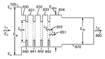
도 8은 광자 에너지 E1을 갖는 제1 파장 λ1의 광(850)을 방출하는 LED와 같은 광원(810), 및 제1 파장의 광의 적어도 일부를 광자 에너지 E2를 갖는 λ2의 광으로 변환하기 위한 반도체 광 변환 구조물(815)을 포함하는 발광 시스템(800)의 개략적인 측면도이다.8 shows a
반도체 광 변환 구조물(815)은 광 변환기(818), 구조물(818) 상에 직접 배치된 구조화된 층(150), 및 구조화된 층 상에 배치된 구조화된 오버코트(160)와 같은 오버코트(160)를 포함한다.The semiconductor
광 변환기(818)는 광원(810)을 향한 제1 윈도우(120); 각각 제1, 제2, 제3 및 제4 포텐셜 웰(840, 841, 842, 843); 4개의 포텐셜 웰을 둘러싸는 각각 제1, 제2, 제3, 제4, 및 제5 광 흡수 층(830, 831, 832, 833, 834); 및 보조 광 흡수 층(870)을 포함한다.The
광 흡수 층(830 내지 834)은 광 흡수 층(130, 131)과 유사하고, 광(850)의 적어도 일부를 흡수하여, 그 결과 광-생성 전자-정공 쌍과 같은 광-생성 캐리어를 생성하며, 이는 광 흡수 층으로부터 포텐셜 웰(840 내지 843)로 확산하거나 이동하고, 여기서 이들은 재결합하여 제2 파장 λ2의 광을 방출한다. 광 흡수 층(830 내지 834)은 캐리어의 재결합 및 제2 파장 λ2의 광(852)의 방출을 위해 광-생성 캐리어가 포텐셜 웰로 효율적으로 확산할 수 있도록 포텐셜 웰에 근접하게 배치된다. 몇몇 경우에, 광 흡수 층(830 내지 834)은 예를 들어 제2 파장에서 포텐셜 웰(840 내지 843)보다 낮은 굴절률을 갖는다.Light absorbing layers 830-834 are similar to light absorbing
몇몇 경우에, 광(850)의 일부는 흡수 층(830 내지 834) 및/또는 포텐셜 웰(840 내지 843)에 의해 흡수되지 않고, 흡수 층 및 포텐셜 웰에 의해 광(851)으로서 투과된다. 예를 들어, 몇몇 경우에, 방출된 광(850)은 도 9에 개략적으로 도시된 세기 스펙트럼(910)을 가질 수 있으며, 여기서 수평 축은 파장이고 수직 축은 임의 단위의 세기이다. 이러한 경우에, 파장 λ1은 피크 세기 Io를 갖는 피크 방출 파장일 수 있고, 광 흡수 층(830 내지 834)의 밴드 갭 파장은 예를 들어 λ1보다 충분히 큰 λabs일 수 있어서, 광(850)의 상당 부분이 흡수 층에 의해 흡수된다. 몇몇 경우에, 포텐셜 웰로 확산하는 광-생성 캐리어 쌍에 대해 상승된 온도에서도 충분한 구속을 제공하도록 λabs는 충분히 작다. 이러한 경우에, 대체로 도 9의 λabs의 오른쪽에 위치되어 있는 스펙트럼(910)의 말단부에 대응하는 광(850)의 일부는 광 흡수 층(830 내지 834) 및/또는 포텐셜 웰(840 내지 843)에 의해 흡수되지 않고, 제1 파장의 광(851)으로서 광 흡수 층 및 포텐셜 웰에 의해 투과된다. 이러한 경우에, 보조 광 흡수 층(870)은 다른 층들에 의해 흡수되지 않은 잔여 또는 나머지 광(851)을 흡수할 수 있다. 몇몇 경우에, 보조 광 흡수 층(870)의 밴드 갭 파장 λlb는 λabs보다 충분히 커서, 본질적으로 모든 광(851)이 보조 광 흡수 층에 의해 흡수된다. 이러한 경우에, 발광 시스템(800)의 출력 광(860)은 본질적으로 λ2에 있으며, λ1의 광의 함량이 전혀 없거나 아주 적다. 이러한 경우에, 보조 광 흡수 층의 밴드 갭 에너지 Elb는 광 흡수 층(830 내지 834)의 밴드 갭 에너지 Eabs보다 작다. 예를 들어, 도 10은 더 작은 Elb와 더 큰 Eabs를 도시하는, 도 8로부터의 광 변환기(818)의 개략적인 밴드 다이어그램(band diagram)이다. 도 10에서, Ec 및 Ev는 각각 전도대 및 가전자대를 나타낸다. 출력 광(860)의 광 세기를 최적화하는 것이 바람직한 때와 같은 몇몇 경우에, 보조 광 흡수 층의 밴드 갭 에너지 Elb는 도 10에 도시된 바와 같이 포텐셜 웰(840 내지 843)의 전이 에너지 Epw보다 크다. 이러한 경우에, Elb는 λ2에서의 광자의 에너지 E2보다 크다.In some cases, a portion of
보조 광 흡수 층(870)의 밴드 갭 에너지가 제5 흡수 층(834)의 밴드 갭 에너지 Eabs보다 작을 때와 같은 몇몇 경우에, 파장 λ2에서의 보조 광 흡수 층(870)의 굴절률은 광 흡수 층(834)의 굴절률보다 크다. 이러한 경우에, 광 변환기(818) 내에서 도파되거나 갇히는 λ2에서의 광학 모드의 전기장은 구조화된 층(150)을 향해 이동한다. 이는 광학 모드의 순간적인 말단을 구조화된 층(150) 및/또는 오버코트(160)로 추가로 확장시킬 수 있으며, 이어서 구조화된 층 및 오버코트에 의해 광(852)의 추출을 향상시키게 된다.In some cases, such as when the band gap energy of the auxiliary
몇몇 경우에, 펌프 광원(810)(도 8 및 도 9 참조)은 제1 파장 λd 및 더 긴 제2 파장 λe의 광을 방출한다. 제1 파장은, 몇몇 경우에, 펌프 광원의 피크 방출 파장 λ1일 수 있다. 광 흡수 층(830 내지 834)은 파장 λd의 광을 흡수할 수 있다. 그러나, 광 흡수 층은 파장 λe의 광을 흡수할 수 없는데, 이는 λe는 광 흡수 층의 밴드 갭 파장 λabs보다 길기 때문이다. 몇몇 경우에, 광 흡수 층은 광(850)의 상당 부분을 흡수할 수 있다. 예를 들어, 그러한 경우에, 광 흡수 층은 광(850)의 적어도 80%, 또는 적어도 85%, 또는 적어도 90%, 또는 적어도 95%를 흡수할 수 있다. 포텐셜 웰(840 내지 843)은 광 흡수 층에 의해 흡수된 광의 적어도 일부를 더 긴 파장의 출력 광(860)으로 변환한다. 보조 광 흡수 층(870)은 제1 파장 λd 및 제2 파장 λe의 광을 흡수할 수 있고, 광원(810)에 의해 방출된 나머지 광을 흡수한다.In some cases, pump light source 810 (see FIGS. 8 and 9) emits light of a first wavelength λ d and a longer second wavelength λ e . The first wavelength may in some cases be the peak emission wavelength λ 1 of the pump light source. Light absorbing layers 830-834 can absorb light of wavelength λ d . However, the light absorbing layer cannot absorb light of wavelength λ e because λ e is longer than the band gap wavelength λ abs of the light absorbing layer. In some cases, the light absorbing layer can absorb a significant portion of
몇몇 경우에, 반도체 광 변환 구조물(815)은 보조 광 흡수 층(870)으로부터 광을 추출하도록 구조화된 층(150) 및 오버코트(160) 내의 구조체 이외의 또는 이에 추가되는 수단을 포함할 수 있다. 예를 들어, 광은 보조 광 흡수 층의 상부 표면을 패터닝 또는 텍스처화(texturing), 예를 들어 조화(roughening)함으로써 추출될 수 있다. 다른 예로서, 광은 보조 광 흡수 층의 외부 표면 상에 광자 결정을 형성함으로써 추출될 수 있다. 예시적인 광자 결정은, 예를 들어 미국 특허 제6,987,288호 및 제7,161,188호에 기술되어 있다. 몇몇 경우에, 광은 보조 광 흡수 층의 출력 표면 상에 광학 요소를 형성함으로써 추출될 수 있으며, 여기서 광학 요소는 임의의 요소일 수 있고, 그렇지 않을 경우 예를 들어 내부 전반사로 인해 보조 광 흡수 층을 빠져나가지 못할 광의 적어도 일부를 추출할 수 있는 임의의 형상을 가질 수 있다. 예시적인 광 추출기는, 예를 들어 공동 소유의 미국 특허 공개 제2007/0284565호; 2006년 11월 17일자로 출원된 공동 소유의 미국 가특허 출원 제60/866,265호; 및 2006년 6월 12일자로 출원된 공동 소유의 미국 가특허 출원 제60/804,544호에 기술되어 있다.In some cases, the semiconductor
몇몇 경우에, 광 흡수 층(834)과 보조 광 흡수 층(870) 중 적어도 하나는 구배형 재료일 수 있다. 이러한 경우, 흡수 층의 두께 방향에 따른 적어도 하나의 위치에서 보조 광 흡수 층(870)의 밴드 갭 에너지 Elb는 광 흡수 층(834)의 최소 밴드 갭 에너지보다 작다. 예를 들어, 도 11은 일정한 밴드 갭 에너지 Eabs를 갖는 광 흡수 층(1120) 및 선형 구배형 보조 광 흡수 층(1130)을 포함하는 광 변환기(1100)의 개략적인 밴드 다이어그램이다. 위치 "X"에서 보조 광 흡수 층(870)의 밴드 갭 에너지 Elb는 광 흡수 층(834)의 밴드 갭 에너지 Eabs보다 작다. 몇몇 경우에, 층의 두께 방향에 따른 적어도 하나의 위치에서 λ2에서의 보조 광 흡수 층(870)의 굴절률은 λ2에서의 광 흡수 층(834)의 최대 굴절률보다 크다.In some cases, at least one of light
일반적으로, 광 변환기(818) 내의 보조 광 흡수 층(870) 및 광 흡수 층(830 내지 834)과 같은 광 흡수 층은 소정 응용에서 실현가능하고 그리고/또는 바람직할 수 있는 임의의 형상의 밴드 다이어그램을 가질 수 있다. 예를 들어, 도 12는 포텐셜 웰(1210), 일정한 밴드 갭 에너지 Eabs를 갖는 광 흡수 층(1220), 및 선형 구배형 밴드 갭을 갖는 보조 광 흡수 층(1230)을 포함하는, 광 변환기(818)와 유사한 광 변환기(1218)의 개략적인 밴드 다이어그램이다. 위치 "X"에서 보조 광 흡수 층(1230)의 밴드 갭 에너지 Elb는 Eabs보다 작고 포텐셜 웰(1210)의 전이 에너지 Etr보다 크다.In general, light absorbing layers, such as auxiliary
다른 예로서, 도 13은 포텐셜 웰(1310), 일정한 밴드 갭 에너지 Eabs를 갖는 광 흡수 층(1320), 및 내장된 포텐셜 또는 양자 웰(1360)을 포함하는 일정한 밴드 갭 에너지 Elb를 갖는 보조 광 흡수 층(1330)을 포함하는 광 변환기(1318)의 개략적인 밴드 다이어그램이다. 밴드 갭 에너지 Elb는 Eabs보다 작고 포텐셜 웰(1310)의 전이 에너지 Etr보다 크다. 또 다른 예로서, 도 14는 포텐셜 웰(1410), 일정한 밴드 갭 에너지 Eabs를 갖는 광 흡수 층(1420), 및 포텐셜 또는 양자 웰(1460)을 포함하는 곡선형 밴드 다이어그램을 갖는 보조 광 흡수 층(1430)을 포함하는 광 변환기(1418)의 개략적인 밴드 다이어그램이다. 보조 광 흡수 층은 위치 "X"에서, Eabs보다 작고 포텐셜 웰(1410)의 전이 에너지 Etr보다 큰 밴드 갭 에너지 Elb를 갖는다.As another example, FIG. 13 shows an auxiliary having a constant band gap energy E lb including a
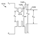
몇몇 경우에, 도 8의 광 변환기 층(818)은, 광-생성 캐리어가 예를 들어 광 변환기의 외부 표면 또는 내부 영역으로 이동하거나 확산하는 것을 방지하기 위해, 윈도우(120)와 같은 또는 윈도우에 더하여 하나 이상의 캐리어 차단 층을 포함할 수 있다. 예를 들어, 도 15는 포텐셜 웰(1510), 일정한 밴드 갭 에너지 Eabs를 갖는 광 흡수 층(1520), 일정한 밴드 갭 에너지 Elb를 갖는 보조 광 흡수 층(1530), 및 층(1520, 1530)들 사이에 배치되며 광 흡수 층(1520) 내의 캐리어가 보조 광 흡수 층(1530)으로 이동, 예를 들어 확산하는 것을 차단하기 위한, 일정한 밴드 갭 에너지 Ecb를 갖는 캐리어 배리어 층(1540)을 포함하는 광 변환기(1518)의 개략적인 밴드 다이어그램이다. 밴드 갭 에너지 Elb는 Eabs보다 작고 포텐셜 웰(1510)의 전이 에너지 Etr보다 크다. 다른 예로서, 도 16은 포텐셜 웰(1610), 일정한 밴드 갭 에너지 Eabs를 갖는 광 흡수 층(1620), 및 보조 광 흡수 층(1630)과, 예를 들어 포텐셜 웰(1610) 및 광 흡수 층(1620) 내의 캐리어가 보조 광 흡수 층(1630)으로 이동하는 것을 차단하기 위한 캐리어 배리어 층(1640)을 포함하는 선형 구배형 영역(1670)을 포함하는 광 변환기(1618)의 개략적인 밴드 다이어그램이다. 위치 "X"에서 보조 광 흡수기의 밴드 갭 에너지 Elb는 Eabs보다 작고 포텐셜 웰(1610)의 전이 에너지 Etr보다 크다. 또 다른 예로서, 도 17은 포텐셜 웰(1710), 일정한 밴드 갭 에너지 Eabs를 갖는 광 흡수 층(1720), 및 보조 광 흡수 층(1730)과, 예를 들어 광 흡수 층(1720) 및/또는 보조 광 흡수 층(1730) 내의 캐리어가 예를 들어 도면에는 명확하게 도시되지 않은 광 변환기(1718)의 출력 표면으로 이동하는 것을 차단하기 위한 캐리어 배리어 층 또는 윈도우(1740)를 포함하는 비-선형 구배형 영역(1770)을 포함하는 광 변환기(1718)의 개략적인 밴드 다이어그램이다. 위치 "X"에서 보조 광 흡수기의 밴드 갭 에너지 Elb는 Eabs보다 작고 포텐셜 웰(1710)의 전이 에너지 Etr보다 크다.In some cases, the
실시예 7:Example 7:
도 1의 광 변환기(118)와 유사한 반도체 광 변환 구조물을 제조하였다. 여러 층들에 대한 상대적인 층 순서와 재료 조성, 두께, 벌크 밴드 갭 에너지, 및 굴절률의 추정 값이 표 II에 요약되어 있다.A semiconductor light conversion structure similar to the
[표 II][Table II]
II-VI 성장을 위한 표면을 제조하기 위해 먼저 GaInAs 버퍼 층을 MBE에 의해 InP 기판 상에 성장시켰다. 그 다음, 광 변환을 위한 II-VI 에피텍셜 층의 성장을 위해 구조물을 초-고진공 전사 시스템을 통해 다른 MBE 챔버로 이동시켰다. 변환기(118)는 4개의 CdZnSe 양자 웰(140)을 포함하였다. 각각의 양자 웰(140)을 GaInN 기반 레이저 다이오드에 의해 방출된 440 ㎚의 청색 광을 흡수할 수 있는 CdMgZnSe 흡수 층들 사이에 개재시켰다.GaInAs buffer layers were first grown on InP substrates by MBE to prepare a surface for II-VI growth. The structure was then moved to another MBE chamber via an ultra-high vacuum transfer system for growth of the II-VI epitaxial layer for light conversion.
구조물을 유리 현미경 슬라이드에 접착식으로 부착시킨 후에 3HCl:1H2O 용액을 이용해 InP 기판을 제거하였다. 에칭제는 GaInAs 버퍼 층(층 #2)에서 정지하였다. 그 후, 버퍼 층을 30 ml 수산화암모늄(30 중량%), 5 ml 과산화수소(30 중량%), 40g 아디프산, 및 200 ml 물의 교반된 용액 내에서 제거하여, 현미경 슬라이드에 부착된 II-VI 광 변환기(118)만을 남겨 두었다.After the structures were adhesively attached to glass microscope slides, the InP substrate was removed using a 3HCl: 1H 2 O solution. The etchant was stopped in the GaInAs buffer layer (layer # 2). The buffer layer is then removed in a stirred solution of 30 ml ammonium hydroxide (30 wt.%), 5 ml hydrogen peroxide (30 wt.%), 40 g adipic acid, and 200 ml water, to attach to the microscope slide II-VI. Only the
도 9의 스펙트럼(910)과 유사한 스펙트럼 및 453 ㎚에서 피크 방출을 갖는 GaInN 청색 펌프 LED를 이용해 윈도우측으로부터 생성된 구조물을 조명할 수 있다. 구조물의 재방출된 출력 광은 양자 웰에 대한 2.305 eV의 전이 에너지에 대응하는 538 ㎚에서의 피크 방출을 가질 수 있다. 표 II에 나타낸 바와 같이, 광 흡수 층은 스펙트럼(910)에서 481 ㎚의 파장 λabs에 대응하는 2.578 eV의 밴드 갭 에너지를 가졌다. λabs의 왼쪽에 있는 스펙트럼(910) 아래의 영역에 대응하는 입사 광의 약 96%는 흡수 층에 의해 흡수될 수 있고, λabs의 오른쪽에 있는 영역에 대응하는 나머지 4%는 보조 광 흡수기에 의해 흡수될 수 있다.GaInN blue pump LEDs with a spectrum similar to
구조물의 캐리어 구속 에너지(포텐셜 웰의 총 깊이)는 0.273 eV (2.578-2.305)였다. 이러한 구조물과 유사하지만 보조 광 흡수 층과 동일한 재료를 갖는 광 흡수 층을 갖는 구조물은 본질적으로 모든 펌프 광을 흡수할 것이지만, 0.185 eV (2.490-2.305)의 감소된 구속 에너지를 가질 것이다. 그 결과, 광 흡수 층 및 보조 광 흡수 층의 조합된 사용은 구속 에너지를 0.185 eV에서 0.273 eV로 증가시켰으며, 이는 거의 48%의 증가이고, 한편 보조 광 흡수 층은 입사 펌프 광의 약 4%만을 흡수하였다.The carrier confinement energy (total depth of potential well) of the structure was 0.273 eV (2.578-2.305). Structures similar to this structure but having a light absorbing layer with the same material as the auxiliary light absorbing layer will absorb essentially all pump light, but will have a reduced restraint energy of 0.185 eV (2.490-2.305). As a result, the combined use of the light absorbing layer and the auxiliary light absorbing layer increased the confinement energy from 0.185 eV to 0.273 eV, which is an increase of almost 48%, while the auxiliary light absorbing layer was only about 4% of the incident pump light. Absorbed.
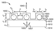
도 1을 다시 참조하면, 도 18에 측면도가 개략적으로 도시되어 있는 광학 구조물(1800)에 대하여 다양한 시스템 파라미터의 함수로서 구조화된 층(150)과 오버코트(160)의 추출 효율을 수치적으로 분석하였다. 광학 구조물은 기판(1810), 기판(1810)의 상부 표면(1812) 상에 직접 배열된 구형 입자들(1855)의 사각 어레이를 포함한 구조화된 층(1850), 및 구조화된 층 상에 그리고 기판의 노출된 영역 상에 직접 배치된 오버코트(1820)를 포함하였다. 기판의 굴절률 n1은 2.646이었다. 입자(1855)의 직경 D는 200 ㎚였고, 입자의 굴절률 n2는 예를 들어 SiO2 입자에 대응하는 1.45였다. 이웃하는 입자들 사이의 간격 P는 500 ㎚였다. 입자는 기판(1810)의 상부 표면(1812)의 50%를 덮었다. 오버코트의 경우, 랜드(land) 두께 t1은 100 ㎚였고, 치수 t2 및 t3는 각각 100 ㎚였으며, t4는 300 ㎚였다. 오버코트의 굴절률 n3는 수치 시뮬레이션 동안 변화되었다.Referring back to FIG. 1, the extraction efficiency of the structured
광원(1805)은 기판의 하부 표면(1814)에 배치하였고, 540 ㎚에서 균일한 광(1807)을 방출하였다. 광학 구조물(1800)의 추출 효율을 모델링하였고, 유효 2차원 유한 차분 시간 영역(Finite Difference Time Domain, FDTD) 접근법을 사용하여 수치적으로 계산하였다. 추출 효율은 방출된 입사 광(1807)의 파워에 대한 출력 광(1840)의 파워의 비로서 정의하였다. 구조화된 층과 오버코트가 없는 경우의 추출 효율은 16.4%였다.A
도 20은 구조화된 층과 구조화된 오버코트의 존재 시에 n3의 함수로서 광학 구조물(1800)의 추출 효율을 도시한다. 공기 오버코트(도 20의 점 P1에 대응하는 n3=1)에 대한 추출 효율은 19.2%였다. 따라서, 오버코트 없이(또는 공기 오버코트에 의해), 입자는 추출 효율을 16.4%에서 19.2%로 증가시켰고, 이는 약 17.1%의 증가이다. SiO2 오버코트에 대응하는 점 P2 (n3=1.45)에서의 추출 효율은 19.8%였으며, 이는 오버코트가 없는 것으로부터는 약 20.7%의 증가이다. 도 20의 점 P3 내지 P5는 각각 Si3N4, ZnS, 및 ZnSe 오버코트에 대응한다. 추출 효율은 일반적으로 영역 Q1에서 선 L1, 영역 Q2에서 선 L2, 및 영역 Q3에서 선 L3를 따른다. Q2에서의 선 L2는 약 2.0 내지 약 2.7 범위인 오버코트 굴절률 n3에 대응하고, 선 L1 및 L3보다 큰 기울기를 갖는다. 영역 Q2는 추출 효율의, 구조화된 오버코트의 굴절률에 대한 더 큰 의존도를 나타낸다.20 shows the extraction efficiency of
몇몇 경우에, 구조화된 층(150)은 오버코트(170)를 적용하기 전에 변형될 수 있다. 예를 들어, 몇몇 경우에, 구조화된 층이 오버코트(170)로 코팅되기 전에 구조화된 층(150) 내의 구조체들 중 적어도 일부의 형상 및/또는 크기가 변형될 수 있다. 하나의 그러한 예시적인 공정이 도 21a 내지 도 21c를 참조하여 설명된다. 도 21a는 반도체 기판(2110) 및 반도체 기판 상에 직접 배치된 구조화된 층(2120)을 포함하는 광학 구조물(2100)의 개략적인 측면도이다. 기판은, 예를 들어 도 1의 제2 윈도우(121) 또는 도 8의 보조 흡수 층(870)과 유사할 수 있다. 몇몇 경우에, 기판(2120)은 다층일 수 있으며, 그 중 하나의 층은 예컨대 보조 흡수 층(870)과 유사할 수 있다.In some cases, structured
구조화된 층(2120)은, 예를 들어 도 1의 구조화된 층(150)과 유사할 수 있다. 구조화된 층(2120)은 기판(2110) 상에 직접 배치된 복수의 이산된 입자(2122)를 포함한다. 몇몇 경우에, 입자(2122)는 유기물, 예컨대 중합체일 수 있다. 예시적인 중합체는 폴리스티렌, 폴리카르보네이트, 폴리(메트)아크릴레이트(예를 들어, 폴리메틸 메타크릴레이트(PMMA)), 폴리올레핀(예를 들어, 폴리프로필렌(PP)), 폴리우레탄, 폴리에스테르(예를 들어, 폴리에틸렌 테레프탈레이트(PET)), 폴리아미드, 폴리이미드, 페놀 수지, 셀룰로오스 다이아세테이트, 셀룰로오스 트라이아세테이트, 스티렌-아크릴로니트릴 공중합체, 에폭시 등을 포함한다.
입자(2122)는 기판(2110)의 상부 표면(2126) 상에 단층을 형성한다. 단층은 개방 영역(2124)과 같은 개방 영역을 포함하여, 기판의 상부 표면을 노출시킨다. 몇몇 경우에, 입자는 에칭제에 입자를 노출시킴으로써 크기가 감소되거나 수축될 수 있다. 예를 들어, 에칭제는 각각의 입자의 일부분을 에칭 제거하여 더 작거나 수축된 입자가 되게 할 수 있다. 예시적인 에칭 방법은 습식 또는 건식 화학적 에칭, 및 반응성 이온 에칭을 포함한다. 몇몇 경우에, 입자는 폴리스티렌이고, 에칭 방법은 산소 플라즈마 또는 반응성 이온 에칭이다.
몇몇 경우에, 입자(2122)는 입자를 충분한 열에 노출시킴으로써 재유동(reflow)되게 된다. 예를 들어, 중합체 입자(2122)는 입자의 융점 또는 그 부근의 온도에서 재유동될 수 있다. 몇몇 경우에, 에칭제와 열이 동시에 입자에 가해짐으로써 입자들 중 적어도 일부를 수축 및 재유동시킬 수 있다. 몇몇 경우에, 에칭 공정은 열을 발생시키며, 이 열이 약간의 추가의 열과 함께 또는 추가의 열 없이 입자를 재유동시킬 수 있다.In some cases,
몇몇 경우에, 구조체(2122)의 평균 크기가 실질적으로 구조체의 표면 밀도를 결정할 수 있고, 에칭 시간과 같은 에칭 정도가 에칭 단계 후의 구조체(구조체(2132))에 의한 면적 피복율을 결정할 수 있다. 몇몇 경우에, 요구되는 초기 평균 구조체 크기 및 에칭 정도가 원하는 표면 구조체 밀도 및 표면 피복율에 기초하여 계산되거나 달리 결정될 수 있다. 예를 들어, 주어진 원하는 입자 밀도에 대하여, 평균 입자 직경 R이 결정될 수 있고, 주어진 원하는 면적 피복율에 대하여 그리고 예를 들어 실험 데이터에 기초하여, 예를 들어 에칭 시간과 같은 에칭 파라미터가 결정될 수 있다. 다음으로, 평균 직경 R을 갖는, 예컨대 조밀 패킹된 입자들의 단층이 표면에 적용되어 원하는 표면 입자 밀도를 제공할 수 있다. 그 다음에, 결정된 에칭 파라미터에 따라 입자가 에칭되어 에칭된 입자에 의한 원하는 표면 피복율을 형성할 수 있다. 몇몇 경우에, 입자는 오버코팅될 수 있다.In some cases, the average size of the
몇몇 경우에, 원하는 최종 표면 피복율을 달성하기 위해, 먼저 원하는 최종 면적 피복율보다 큰 초기 면적 피복율이 되도록 복수의 구조체가 상부 표면(2126) 상에 배치된다. 다음으로, 구조체들 중 적어도 일부가 초기 면적 피복율을 원하는 최종 면적 피복율로 감소시키도록 충분하게 수축된다. 몇몇 경우에, 구조체들 중 적어도 일부는 재유동될 수 있다. 몇몇 경우에, 그 다음, 구조체는 수축된 구조체 및 덮이지 않은 영역의 상부 표면을 덮도록 오버코트로 코팅된다.In some cases, to achieve the desired final surface coverage, a plurality of structures are first disposed on the
충분한 열과 하나 이상의 에칭제를 가한 후에, 광학 구조물(2100)은 도 21b에 개략적으로 도시된 광학 구조물(2150)로 변형된다. 특히, 구조화된 층(2120)은, 층(2120) 내의 입자(2122)가 부분적으로 에칭되고 재유동된 후에, 구조화된 층(2130)으로 변경 또는 변형된다. 구조화된 층(2130)은, 대응하는 입자(2122)보다 작으며 열에의 노출로 인해 재유동된 입자(2132)를 포함한다. 재유동 후에, 입자(2132)는 평평한 하면(2134)을 갖는다. 몇몇 경우에, 입자(2132)는 돔형 또는 원추형이다. 몇몇 경우에, 입자를 재유동 및 수축시키는 단계는 동시에 또는 일제히 수행될 수 있다. 몇몇 경우에, 두 단계는 순차적으로 수행될 수 있다. 예를 들어, 입자가 에칭제에 의해 크기가 감소된 후에, 에칭된 입자를 재유동시키도록 가열 단계가 이어질 수 있다.After applying sufficient heat and one or more etchant, the
몇몇 경우에, 복수의 입자에 의한 기판(2110)의 상부 표면(2126)의 피복율은 입자에 에칭제 및 열을 가한 후에 감소한다. 예를 들어, 그러한 경우에, 입자(2122)는 도 21a의 상부 표면(2126)을 제1 피복율로 덮고, 입자(2132)는 도 21b의 상부 표면(2126)을 제2 피복율로 덮으며, 여기서 제2 피복율은 제1 피복율보다 작다.In some cases, the coverage of the
몇몇 경우에, 수축 단계는 입자의 평균 측방향 크기와 같은 평균 크기를 적어도 10%, 또는 적어도 20%, 또는 적어도 30%, 또는 적어도 40%, 또는 적어도 50%, 또는 적어도 60%, 또는 적어도 70%만큼 감소시킬 수 있다. 몇몇 경우에, 복수의 구조체에 의한 기판의 상부 표면의 면적 피복율은 수축 단계 후에 감소한다. 예를 들어, 그러한 경우, 면적 피복율은 적어도 10%, 또는 적어도 20%, 또는 적어도 30%, 또는 적어도 40%, 또는 적어도 50%만큼 감소할 수 있다.In some cases, the shrinking step results in at least 10%, or at least 20%, or at least 30%, or at least 40%, or at least 50%, or at least 60%, or at least 70 an average size, such as the mean lateral size of the particles. Can be reduced by%. In some cases, the area coverage of the upper surface of the substrate by the plurality of structures decreases after the shrinking step. For example, in such a case, the area coverage can be reduced by at least 10%, or at least 20%, or at least 30%, or at least 40%, or at least 50%.
몇몇 경우에, 광학 구조물(2150)은 오버코트(2160)로 코팅되어, 도 21c에 개략적으로 도시된 광학 구조물(2180)을 형성한다. 오버코트(2160)는 복수의 입자(2132) 및 개방 영역(2124)과 같은 개방 영역 내의 기판(2110)의 상부 표면을 덮는다.In some cases,
기판(2110)은, 예를 들어 스펙트럼의 가시 영역에서 굴절률 n1을 가지며, 구조화된 층(2130) 내의 입자(2132)는 굴절률 n2를 갖고, 오버코트(2160)는 굴절률 n3를 갖는다. 몇몇 경우에, n2는 n1보다 작다. 예를 들어, 그러한 경우, 기판(2110)은 약 2 내지 약 2.7, 또는 약 2 내지 약 2.5 범위의 굴절률을 갖는 반도체 재료를 포함하고, 입자(2132)는 약 1.5 내지 약 1.8 범위의 굴절률을 갖는 중합체를 포함한다. 몇몇 경우에, n3는 n1보다 크다. 예를 들어, 그러한 경우, 기판(2110)은 약 2 내지 약 2.3 범위의 굴절률을 갖는 반도체 재료를 포함하고, 오버코트(2160)는 약 2.3 내지 약 2.7 범위의 굴절률을 갖는 상이한 반도체를 포함한다.The
실시예 8:Example 8:
실시예 1에 약술한 공정을 사용하여 반도체 광 변환 구조물을 제조하였다. 구조물의 계산된 EQE는 15.29%였다. 도 21a의 구조화된 층(2120)과 유사한 구조화된 층이 되도록, 구조물의 흡수기측을 폴리스티렌(PS) 미소구체로 코팅하였다. 미소구체는 약 1000 ㎚의 평균 직경을 가졌고, 브이더블유알 사이언티픽 프로덕츠(VWR Scientific Products)(미국 뉴저지주 사우스 플레인필드)로부터 입수하였다. 미소구체의 굴절률은 약 1.59였고, 구조물의 흡수기의 굴절률은 약 2.6이었다. 미소구체를 10 중량%의 고형물 함량으로 H2O 중에 분산시켰다. 스핀-온(spin-on) 코팅 방법을 사용하여 약 200 rpm의 속도에서 약 20초 동안 그리고 이어서 약 5000 rpm의 속도에서 약 5초 동안 용액을 흡수기의 상부 표면(도 21a의 상부 표면(2126))에 적용하였다. 도 22a는 광 변환 구조물의 상부 표면 상의 조밀 패킹된 미소구체 PS 입자를 도시하는 생성된 샘플의 SEM 이미지이다. 미소구체에 의한 상부 표면의 면적 피복율은 약 90%였고, 생성된 샘플의 계산된 EQE는 22.9%였다. 따라서, PS 입자는 EQE를 15.29%에서 22.9%로 증가시켰고, 이는 약 49.8%의 증가이다. 그 다음, 샘플을 산소 플라즈마(6 mT, 80 W의 RF 전력, 및 1200 W의 유도 결합 플라즈마 전력)로 에칭하여 재유동시켰고 입자의 크기를 감소시켰다. 입자에 의한 그 결과의 표면 피복율은 약 64%였다. 따라서, 에칭 단계는 면적 피복율을 약 90%에서 약 64%로 감소시켰다. 도 22b는 생성된 샘플의 SEM 이미지이다. 입자는 평평한 하면을 갖는 원추형 또는 돔형이었다. 생성된 샘플의 계산된 EQE는 27.8%였다. 다음으로, 샘플을 진공 증발 공정을 사용하여 ZnS로 오버코팅하였다. 오버코트의 두께는 약 400 ㎚였고, ZnS 오버코트의 굴절률은 약 2.4였다. 도 22c는 생성된 샘플의 SEM 이미지이다. 생성된 샘플의 계산된 EQE는 37.8%였다. 따라서, ZnS 오버코트의 추가는 EQE를 27.8%에서 37.8%로 증가시켰고, 이는 약 36%의 증가이다.A semiconductor light converting structure was prepared using the process outlined in Example 1. The calculated EQE of the structure was 15.29%. The absorber side of the structure was coated with polystyrene (PS) microspheres to be a structured layer similar to the structured
실시예 9:Example 9:
실시예 1에 약술한 공정을 사용하여 반도체 광 변환 구조물을 제조하였다. 구조물의 계산된 EQE는 17.65%였다. 도 21a의 구조화된 층(2120)과 유사한 구조화된 층이 되도록, 구조물의 흡수기측을 폴리스티렌(PS) 미소구체로 코팅하였다. 미소구체는 약 500 ㎚의 평균 직경을 가졌고, 브이더블유알 사이언티픽 프로덕츠(미국 뉴저지주 사우스 플레인필드)로부터 입수하였다. 미소구체의 굴절률은 약 1.59였고, 구조물의 흡수기의 굴절률은 약 2.6이었다. 미소구체를 1.5 중량%의 고형물 함량으로 H2O 중에 분산시켰다. 딥 코팅 방법을 사용하여 약 65 ㎜/분의 속도에서 용액을 흡수기의 상부 표면(도 21a의 상부 표면(2126))에 적용하였다. 샘플을 단일 회 딥 코팅하였다. 생성된 샘플의 계산된 EQE는 26.40%였다. 따라서, PS 입자는 EQE를 17.65%에서 26.40%로 증가시켰고, 이는 약 49.6%의 증가이다. 그 다음, 샘플을 산소 플라즈마(200 mT, 200 ㎽, 및 20.32 ㎝ (8 인치) 직경 평판(platen))로 에칭하여 입자를 약간 수축시켰고 재유동시켰다. 생성된 입자는 평평한 하면을 갖는 원추형 또는 돔형이었다. 다음으로, 샘플을 진공 증발 공정을 사용하여 ZnS로 오버코팅하였다. 오버코트의 두께는 약 400 ㎚였고, ZnS 오버코트의 굴절률은 약 2.4였다. 생성된 샘플의 계산된 EQE는 35.5%였다. 따라서, ZnS 오버코트의 추가는 EQE를 26.4%에서 35.5%로 증가시켰고, 이는 약 34.5%의 증가이다.A semiconductor light converting structure was prepared using the process outlined in Example 1. The calculated EQE of the structure was 17.65%. The absorber side of the structure was coated with polystyrene (PS) microspheres to be a structured layer similar to the structured
도 23은 제1 파장 λ1의 광(850)을 방출하는 LED 광원, 및 광(850)의 적어도 일부를 더 긴 제2 파장 λ2의 광(852)으로 변환하는 광 변환 층(2315)을 포함하는 광원(2300)의 개략적인 측면도이다. 광 변환 구조물(2315)은 기판(2320) 상에 배치된, 제1 굴절률 n1을 갖는 인광체 슬래브(2330)를 포함한다. 인광체 슬래브(2330)는 광(850)의 적어도 일부를 흡수하고, 흡수된 광의 적어도 일부를 파장 λ2의 광(852)으로서 재방출한다. 인광체 슬래브(2330)에 사용될 수 있는 예시적인 인광체는 스트론튬 티오갈레이트, 도핑된 GaN, 구리-활성화된 황화아연, 및 은-활성화된 황화아연을 포함한다. 다른 유용한 인광체는 도핑된 YAG, 실리케이트, 옥시질화규소, 질화규소, 및 알루미네이트 기반 인광체를 포함한다. 이러한 인광체의 예는 Ce:YAG, SrSiON:Eu, SrBaSiO:Eu, SrSiN:Eu, 및 BaSrSiN:Eu를 포함한다.FIG. 23 shows an LED light source that emits
기판(2320)은 응용에 적합할 수 있는 임의의 재료를 포함할 수 있다. 예시적인 재료는 유리, 중합체, 세라믹, 예컨대 알루미나, 사파이어, 및 금속, 예컨대 광이 통과할 수 있게 하는 하나 이상의 투명 개방부 또는 개구를 포함하는 금속을 포함한다. 몇몇 경우에, 기판(2320)은 실질적으로 제1 파장에서 광학적으로 투과성이다. 몇몇 경우에, 기판은 λ1에서 불투명할 수 있다. 이러한 경우에, 기판은 광(850)이 기판을 통과할 수 있는 하나 이상의 광학적 또는 다른 개방부를 포함할 수 있다. 몇몇 경우에, 기판(2320)은 히트 싱크 또는 λ2의 반사기와 같이 도 23에서는 명확하게 도시되지 않은 다른 기능 층을 포함할 수 있다.
광 변환 구조물(2315)은 인광체 슬래브(2330) 상에 배치된 구조화된 층(150)을 추가로 포함한다. 구조화된 층(150)은 인광체 슬래브의 제1 굴절률 n1보다 작은 제2 굴절률 n2를 갖는다. 구조화된 층은 인광체 슬래브 상에 직접 배치된 복수의 구조체(151) 및 인광체 슬래브를 노출시키는 복수의 개방부(2305)를 포함한다. 광 변환 구조물(2315)은 적어도 구조화된 층(150)의 일부분 및 개방부(2305)와 같은 복수의 개방부 내의 인광체 슬래브의 일부분 상에 직접 배치된, 오버코트(160)와 유사한 구조화된 오버코트(2360)를 추가로 포함한다. 구조화된 오버코트(2360)는 제2 굴절률 n2보다 큰 제3 굴절률 n3를 갖는다.
몇몇 경우에, 구조화된 오버코트(2360)는, 갇힌 광의 순간적인 말단을 구조화된 오버코트로 더 확장시킴으로써, 인광체 슬래브에 갇히는 제2 파장 λ2의 광의 추출을 향상시킬 수 있다. 말단 확장은 구조체(151)에 의해 갇힌 광의 산란을 증가시킬 수 있어서, 인광체 슬래브로부터의 갇힌 광의 추출이 증가된다.In some cases, structured
몇몇 경우에, 구조화된 층(150)은 실질적으로 제2 파장에서 광학적으로 투명하다. 몇몇 경우에, 구조화된 오버코트(2360)는 실질적으로 제2 파장에서 광학적으로 투명하다. 몇몇 경우에, 구조화된 층(150) 내의 복수의 구조체는 이산된 입자들과 같은 복수의 이산된 구조체를 포함하며, 여기서 몇몇 경우에 복수의 이산된 입자의 상당한 분율은 실질적으로 구형이다. 몇몇 경우에, 구조화된 층(150) 내의 복수의 구조체는 복수의 상호연결된 구조체를 포함한다.In some cases, structured
몇몇 경우에, 구조화된 오버코트(2360)는 Si3N4, ZnS, ZnSe, ZnSSe, ITO, TiO2, ZrO2, Ta2O5, HfO2, 및 실리케이트, 예컨대 실리케이트 유리 중 적어도 하나를 포함한다. 몇몇 경우에, 구조화된 오버코트(2360)는 반도체를 포함한다. 몇몇 경우에, 구조화된 오버코트(2360)의 구조화된 외부 표면(2361)은 구조화된 층(150)의 구조화된 외부 표면(2362)과 정합한다.In some cases, structured
도 18의 광학 구조물(1800)을 사용하여 다양한 시스템 파라미터의 함수로서 광 변환 구조물(2315)의 추출 효율을 수치적으로 분석하였다. 기판의 굴절률 n1은 1.84였으며, 이는 인광체 슬래브(2330)와 같은 인광체 슬래브에 대한 전형적인 값이다. 입자(1855)의 직경 D는 200 ㎚였고, 입자의 굴절률 n2는 예를 들어 SiO2 입자에 대응하는 1.45였다. 이웃하는 입자들 사이의 간격 P는 500 ㎚였다. 입자는 기판(1810)의 상부 표면(1812)의 50%를 덮었다. 오버코트의 경우, 랜드 두께 t1은 100 ㎚였고, 치수 t2 및 t3는 각각 100 ㎚였으며, t4는 300 ㎚였다. 오버코트의 굴절률 n3는 수치 시뮬레이션 동안 변화되었다.The
광원(1805)은 기판의 하부 표면(1814)에 배치하였고, 540 ㎚에서 균일한 광(1807)을 방출하였다. 광학 구조물(1800)의 추출 효율을 모델링하였고, 유효 2차원 유한 차분 시간 영역(FDTD) 접근법을 사용하여 수치적으로 계산하였다.A
도 24는 구조화된 층과 오버코트의 존재 시에 n3의 함수로서 광학 구조물(1800)의 추출 효율을 도시한다. SiO2 오버코트에 대응하는 점 Q1 (n3=1.45)에서의 추출 효율은 40.5%였다. 도 24의 점 Q2 및 Q3는 각각 Si3N4 및 TiO2오버코트에 대응한다. 약 1.35 내지 약 2.2, 또는 약 1.45 내지 약 2.2 범위의 n3에 대하여, 추출 효율은 적어도 약 40%이다. 몇몇 경우에, 오버코트는 약 1.38 내지 약 1.39 범위의 굴절률을 갖는 MgF2를 포함할 수 있다. 몇몇 경우에, 오버코트는 다공성 코팅을 포함할 수 있다. 예를 들어, 오버코트는 약 1.45 미만의 굴절률, 예를 들어 약 1.4, 또는 약 1.35, 또는 약 1.30, 또는 약 1.29의 굴절률을 갖는 다공성 SiO2 코팅을 포함할 수 있다.24 shows the extraction efficiency of the
본 명세서에 사용되는 바와 같이, "수직", "수평", "위", "아래", "좌측", "우측", "상부"와 "하부", "상단"과 "하단" 및 기타 유사 용어와 같은 용어는 도면에 도시된 바와 같은 상대 위치를 지칭한다. 일반적으로, 물리적 실시 형태들이 상이한 배향을 가질 수 있고, 그 경우에, 용어는 소자의 실제 배향에 대해 변형된 상대 위치를 지칭하는 것으로 의도된다. 예를 들어, 도 1의 구성이 도면의 배향에 비교할 때 역전되어 있더라도, 제1 흡수 층(130)은 여전히 포텐셜 웰(140) "아래에" 있는 것으로 고려된다.As used herein, "vertical", "horizontal", "up", "down", "left", "right", "top" and "bottom", "top" and "bottom" and other similarities Terms, such as terms, refer to relative positions as shown in the figures. In general, physical embodiments may have different orientations, in which case the term is intended to refer to a modified relative position with respect to the actual orientation of the device. For example, although the configuration of FIG. 1 is reversed as compared to the orientation of the figure, the first
본 발명의 다양한 태양의 설명을 용이하게 하기 위해 본 발명의 특정 실시예들이 상기에 상세하게 기술되었지만, 실시예들의 상세 사항으로 본 발명을 제한하고자 하는 것이 아님을 이해하여야 한다. 오히려, 첨부된 특허청구범위에 의해 한정된 바와 같은 본 발명의 사상 및 범위 내에 속하는 모든 변형, 실시 형태, 및 대안들을 포함하고자 한다.While specific embodiments of the invention have been described in detail above to facilitate describing various aspects of the invention, it should be understood that the intention is not to limit the invention to the details of the embodiments. Rather, the intention is to cover all modifications, embodiments, and alternatives falling within the spirit and scope of the invention as defined by the appended claims.
Claims (27)
인광체 슬래브 상에 배치되며 제1 굴절률보다 작은 제2 굴절률을 갖고, 인광체 슬래브 상에 직접 배치되는 복수의 구조체 및 인광체 슬래브를 노출시키는 복수의 개방부를 포함하는 구조화된 층; 및
적어도 구조화된 층의 일부분 및 복수의 개방부 내의 인광체 슬래브의 일부분 상에 직접 배치되며, 제2 굴절률보다 큰 제3 굴절률을 갖는 구조화된 오버코트(overcoat)
를 포함하는 광 변환 구조물.A phosphor slab having a first index of refraction for converting at least a portion of the light of the first wavelength into light of a longer second wavelength;
A structured layer disposed on the phosphor slab and having a second refractive index less than the first refractive index, the structured layer comprising a plurality of structures disposed directly on the phosphor slab and a plurality of openings exposing the phosphor slab; And
A structured overcoat having a third refractive index that is disposed directly on at least a portion of the structured layer and a portion of the phosphor slab in the plurality of openings, the second refractive index being greater than the second refractive index.
Light conversion structure comprising a.
광 변환 구조물에 의해 제2 파장의 광으로 적어도 일부가 변환되는 제1 파장의 광을 방출하는 LED
를 포함하는 전계발광 요소(electroluminescent element); 및
전계발광 요소를 봉지하는 봉지재
를 포함하는 발광 시스템.The light conversion structure of claim 1;
LEDs emitting light of a first wavelength at least partially converted to light of a second wavelength by a light converting structure
An electroluminescent element comprising an electroluminescent element; And
Encapsulant encapsulating electroluminescent element
Light emitting system comprising a.
Applications Claiming Priority (2)
| Application Number | Priority Date | Filing Date | Title |
|---|---|---|---|
| US7593508P | 2008-06-26 | 2008-06-26 | |
| US61/075,935 | 2008-06-26 |
Publications (1)
| Publication Number | Publication Date |
|---|---|
| KR20110031957A true KR20110031957A (en) | 2011-03-29 |
Family
ID=41445190
Family Applications (1)
| Application Number | Title | Priority Date | Filing Date |
|---|---|---|---|
| KR1020117001595A KR20110031957A (en) | 2008-06-26 | 2009-06-03 | Light converting construction |
Country Status (7)
| Country | Link |
|---|---|
| US (1) | US8461608B2 (en) |
| EP (1) | EP2308103A4 (en) |
| JP (1) | JP5475767B2 (en) |
| KR (1) | KR20110031957A (en) |
| CN (1) | CN102124581B (en) |
| TW (1) | TWI487136B (en) |
| WO (1) | WO2009158159A2 (en) |
Families Citing this family (7)
| Publication number | Priority date | Publication date | Assignee | Title |
|---|---|---|---|---|
| US8324000B2 (en) | 2008-06-26 | 2012-12-04 | 3M Innovative Properties Company | Method of fabricating light extractor |
| KR20110030630A (en) | 2008-06-26 | 2011-03-23 | 쓰리엠 이노베이티브 프로퍼티즈 컴파니 | Semiconductor light converting construction |
| WO2010000665A1 (en) * | 2008-06-30 | 2010-01-07 | Santaris Pharma A/S | Antidote oligomers |
| WO2010027650A1 (en) * | 2008-09-04 | 2010-03-11 | 3M Innovative Properties Company | Light source with improved monochromaticity |
| US8933526B2 (en) * | 2009-07-15 | 2015-01-13 | First Solar, Inc. | Nanostructured functional coatings and devices |
| JP2015038978A (en) * | 2013-07-17 | 2015-02-26 | 日本電気硝子株式会社 | Wavelength conversion member |
| TWI539632B (en) * | 2013-11-04 | 2016-06-21 | 隆達電子股份有限公司 | Light emitting diode structure |
Family Cites Families (44)
| Publication number | Priority date | Publication date | Assignee | Title |
|---|---|---|---|---|
| JP2756050B2 (en) * | 1992-03-03 | 1998-05-25 | キヤノン株式会社 | Photovoltaic device |
| JP4066620B2 (en) * | 2000-07-21 | 2008-03-26 | 日亜化学工業株式会社 | LIGHT EMITTING ELEMENT, DISPLAY DEVICE HAVING LIGHT EMITTING ELEMENT AND METHOD FOR MANUFACTURING DISPLAY DEVICE |
| FR2824228B1 (en) * | 2001-04-26 | 2003-08-01 | Centre Nat Rech Scient | ELECTROLUMINESCENT DEVICE WITH LIGHT EXTRACTOR |
| US6580740B2 (en) * | 2001-07-18 | 2003-06-17 | The Furukawa Electric Co., Ltd. | Semiconductor laser device having selective absorption qualities |
| US6815354B2 (en) * | 2001-10-27 | 2004-11-09 | Nutool, Inc. | Method and structure for thru-mask contact electrodeposition |
| JP3817471B2 (en) * | 2001-12-11 | 2006-09-06 | 富士写真フイルム株式会社 | Porous structure and structure, and production method thereof |
| US7016384B2 (en) * | 2002-03-14 | 2006-03-21 | Fuji Photo Film Co., Ltd. | Second-harmonic generation device using semiconductor laser element having quantum-well active layer in which resonator length and mirror loss are arranged to increase width of gain peak |
| DE20321614U1 (en) * | 2002-04-05 | 2008-06-12 | Citizen Electronics Co., Ltd., Fujiyoshida-shi | Light emitting diode |
| US7170097B2 (en) * | 2003-02-14 | 2007-01-30 | Cree, Inc. | Inverted light emitting diode on conductive substrate |
| CN100337337C (en) | 2003-07-18 | 2007-09-12 | 财团法人工业技术研究院 | Omnidirectional reflector and luminous apparatus produced thereby |
| JP4703108B2 (en) * | 2003-09-10 | 2011-06-15 | 三星モバイルディスプレイ株式會社 | Light emitting element substrate and light emitting element using the same |
| JP4232585B2 (en) * | 2003-09-17 | 2009-03-04 | 豊田合成株式会社 | Light emitting device |
| JP4093943B2 (en) * | 2003-09-30 | 2008-06-04 | 三洋電機株式会社 | LIGHT EMITTING ELEMENT AND MANUFACTURING METHOD THEREOF |
| US7408201B2 (en) * | 2004-03-19 | 2008-08-05 | Philips Lumileds Lighting Company, Llc | Polarized semiconductor light emitting device |
| US7361938B2 (en) * | 2004-06-03 | 2008-04-22 | Philips Lumileds Lighting Company Llc | Luminescent ceramic for a light emitting device |
| JP4717882B2 (en) * | 2004-06-14 | 2011-07-06 | コーニンクレッカ フィリップス エレクトロニクス エヌ ヴィ | LED with improved emission profile |
| US7161188B2 (en) * | 2004-06-28 | 2007-01-09 | Matsushita Electric Industrial Co., Ltd. | Semiconductor light emitting element, semiconductor light emitting device, and method for fabricating semiconductor light emitting element |
| TWI233704B (en) | 2004-08-20 | 2005-06-01 | Univ Nat Central | Semiconductor structure with white light generator and amplifier |
| JP4959127B2 (en) * | 2004-10-29 | 2012-06-20 | 三菱重工業株式会社 | Photoelectric conversion device and substrate for photoelectric conversion device |
| US7402831B2 (en) * | 2004-12-09 | 2008-07-22 | 3M Innovative Properties Company | Adapting short-wavelength LED's for polychromatic, broadband, or “white” emission |
| US7524686B2 (en) * | 2005-01-11 | 2009-04-28 | Semileds Corporation | Method of making light emitting diodes (LEDs) with improved light extraction by roughening |
| TW200637037A (en) * | 2005-02-18 | 2006-10-16 | Sumitomo Chemical Co | Semiconductor light-emitting element and fabrication method thereof |
| JP2006261659A (en) | 2005-02-18 | 2006-09-28 | Sumitomo Chemical Co Ltd | Manufacturing method for semiconductor light emitting device |
| US7602118B2 (en) * | 2005-02-24 | 2009-10-13 | Eastman Kodak Company | OLED device having improved light output |
| JP2006278751A (en) * | 2005-03-29 | 2006-10-12 | Mitsubishi Cable Ind Ltd | Garium nitride-based semiconductor light emitting element |
| JP2006294343A (en) * | 2005-04-07 | 2006-10-26 | Mitsubishi Rayon Co Ltd | Planar led light source device |
| JP4466571B2 (en) * | 2005-05-12 | 2010-05-26 | 株式会社デンソー | Driver status detection device, in-vehicle alarm device, driving support system |
| JP2007005173A (en) * | 2005-06-24 | 2007-01-11 | Toshiba Matsushita Display Technology Co Ltd | Display device |
| KR20070011041A (en) | 2005-07-19 | 2007-01-24 | 주식회사 엘지화학 | Light emitting diode device having advanced light extraction efficiency and preparation method thereof |
| US7196354B1 (en) * | 2005-09-29 | 2007-03-27 | Luminus Devices, Inc. | Wavelength-converting light-emitting devices |
| US7990055B2 (en) * | 2006-03-03 | 2011-08-02 | Koninklijke Philips Electronics N.V. | Electroluminescent arrangement having detached electrode and method of fabricating the same |
| KR100799859B1 (en) * | 2006-03-22 | 2008-01-31 | 삼성전기주식회사 | White light emitting device |
| JP2007273746A (en) | 2006-03-31 | 2007-10-18 | Sumitomo Chemical Co Ltd | Method of micromachining solid-state surface and light emitting element |
| US20090206301A1 (en) * | 2006-05-29 | 2009-08-20 | Koninklijke Philips Electronics N.V. | Inorganic phosphor bodies for light emitting diodes |
| JP2009540558A (en) * | 2006-06-08 | 2009-11-19 | コーニンクレッカ フィリップス エレクトロニクス エヌ ヴィ | Light emitting device |
| US20070284565A1 (en) * | 2006-06-12 | 2007-12-13 | 3M Innovative Properties Company | Led device with re-emitting semiconductor construction and optical element |
| JP2007335798A (en) * | 2006-06-19 | 2007-12-27 | Toyoda Gosei Co Ltd | Light-emitting device |
| KR100798863B1 (en) | 2006-06-28 | 2008-01-29 | 삼성전기주식회사 | GaN type light emitting diode device and method of manufacturing the same |
| KR101294008B1 (en) * | 2006-07-24 | 2013-08-07 | 삼성디스플레이 주식회사 | Backlight assembly, method of manufacturing the same and display device having the same |
| SG140481A1 (en) * | 2006-08-22 | 2008-03-28 | Agency Science Tech & Res | A method for fabricating micro and nano structures |
| KR20110030630A (en) * | 2008-06-26 | 2011-03-23 | 쓰리엠 이노베이티브 프로퍼티즈 컴파니 | Semiconductor light converting construction |
| US20110101402A1 (en) * | 2008-06-26 | 2011-05-05 | Jun-Ying Zhang | Semiconductor light converting construction |
| US8324000B2 (en) * | 2008-06-26 | 2012-12-04 | 3M Innovative Properties Company | Method of fabricating light extractor |
| KR20110031953A (en) | 2008-06-26 | 2011-03-29 | 쓰리엠 이노베이티브 프로퍼티즈 컴파니 | Semiconductor light converting construction |
-
2009
- 2009-06-03 EP EP09770693.1A patent/EP2308103A4/en not_active Withdrawn
- 2009-06-03 CN CN200980132106.4A patent/CN102124581B/en not_active Expired - Fee Related
- 2009-06-03 KR KR1020117001595A patent/KR20110031957A/en not_active Application Discontinuation
- 2009-06-03 JP JP2011516395A patent/JP5475767B2/en not_active Expired - Fee Related
- 2009-06-03 WO PCT/US2009/046083 patent/WO2009158159A2/en active Application Filing
- 2009-06-03 US US13/000,608 patent/US8461608B2/en not_active Expired - Fee Related
- 2009-06-15 TW TW098119987A patent/TWI487136B/en not_active IP Right Cessation
Also Published As
| Publication number | Publication date |
|---|---|
| JP5475767B2 (en) | 2014-04-16 |
| EP2308103A4 (en) | 2014-04-30 |
| EP2308103A2 (en) | 2011-04-13 |
| JP2011526076A (en) | 2011-09-29 |
| WO2009158159A2 (en) | 2009-12-30 |
| US20110101382A1 (en) | 2011-05-05 |
| CN102124581B (en) | 2013-09-25 |
| WO2009158159A3 (en) | 2010-03-04 |
| US8461608B2 (en) | 2013-06-11 |
| TWI487136B (en) | 2015-06-01 |
| CN102124581A (en) | 2011-07-13 |
| TW201007990A (en) | 2010-02-16 |
Similar Documents
| Publication | Publication Date | Title |
|---|---|---|
| US9053959B2 (en) | Semiconductor light converting construction | |
| US8324000B2 (en) | Method of fabricating light extractor | |
| KR20110031953A (en) | Semiconductor light converting construction | |
| US10128418B2 (en) | LED cap containing quantum dot phosphors | |
| US10461230B2 (en) | Light emitting diode component | |
| US8461608B2 (en) | Light converting construction | |
| KR20120038539A (en) | Pixelated led | |
| KR102102699B1 (en) | Quantum dot-based color-converted light-emitting device and method for manufacturing the same | |
| US8835963B2 (en) | Light converting and emitting device with minimal edge recombination | |
| US20110101402A1 (en) | Semiconductor light converting construction |
Legal Events
| Date | Code | Title | Description |
|---|---|---|---|
| A201 | Request for examination | ||
| E902 | Notification of reason for refusal | ||
| E601 | Decision to refuse application |